arm cortex-a*
TRANSCRIPT

ARM Cortex-A* Brian Eccles, Riley Larkins, Kevin Mee, Fred Silberberg, Alex Solomon, Mitchell Wills
The ARM CortexA product line has changed significantly since the introduction of the
CortexA8 in 2005. ARM’s next major leap came with the CortexA9 which was the first design to incorporate multiple cores. The next advance was the development of the big.LITTLE architecture, which incorporates both high performance (A15) and high efficiency(A7) cores. Most recently the A57 and A53 have added 64bit support to the product line.
The ARM Cortex series cores are all made up of the main processing unit, a L1
instruction cache, a L1 data cache, an advanced SIMD core and a floating point core. Each processor then has an additional L2 cache shared between all cores (if there are multiple), debug support and an interface bus for communicating with the rest of the system. Multicore processors (such as the A53 and A57) also include additional hardware to facilitate coherency between cores.
The ARM CortexA57 is a 64bit processor that supports 1 to 4 cores. The instruction pipeline in each core supports fetching up to three instructions per cycle to send down the pipeline. The instruction pipeline is made up of a 12 stage in order pipeline and a collection of parallel pipelines that range in size from 3 to 15 stages as seen below. The ARM CortexA53 is similar to the A57, but is designed to be more power efficient at the cost of processing power.

The A57 in order pipeline is made up of 5 stages of instruction fetch and 7 stages of instruction decode and register renaming. Instruction fetch will fetch three instructions from the L1 instruction cache in one cycle. It also includes a branch prediction core with a number of different branch prediction methods. Unconditional branches are always predicted to be taken and in addition to unconditional function calls and returns. A return stack is used to predict the destination of a return. A 2 bit dynamic prediction buffer is also included to predict conditional branches.
The instruction decode section support three different ARM instruction sets: A32, T32 and A64. This section also performs register renaming to allow for out of order instruction execution and removes write after write and write after read hazards. Like the fetch section it also supports 3 instructions per cycle. The A32 instruction set is part of the ARMv7 specification uses fixed length 32bit instructions and operates in a 32bit addressing mode. It is designed to be used for high performance applications and contains conditional versions of most instructions. The T32 instruction set also executes in 32bit addressing mode, uses 16bit or 32bit instructions and is designed for higher code density. Finally, the new A64 instruction set from the new ARMv8 specification adds support for executing in a 64bit addressing mode. It uses 32bit instruction like the A32 instruction set, but includes significantly fewer conditional instructions.
The outoforder pipeline has eight, largely independent pipelines that are able to
execute in parallel. Microoperations from the decode stage are queued in the dispatch stage, are then dispatched to one of the eight pipelines, which range between one and ten stages, and finally end at the writeback stage. At the dispatch stage operations are queued by both issue port from the decode stage, and the specific pipeline each is destined for. Each pipeline path can queue up to three operations, one from each issue port, for a maximum of 24 queued operations at once. While the dispatch stage can only receive three operations per cycle, if there are more queued that become available to execute, more than three can be dispatched as long as constraints on pipeline resources are satisfied.
The simplest outoforder pipeline is the branch path. It is one stage long, has a typical
latency of one cycle, and serves primarily as a validator for the more sophisticated branch prediction logic that is used in the inorder section of the pipeline. Some of its operations also

make use of the simple integer pipelines for offset calculations. Load and store operations are handled by a pair of pipelines allowing for one load and one store operation per cycle. Like the branch pipeline, some operations also require a simple integer pipeline for offset calculations.
Basic integer operations are handled by two identical pipelines.Each can perform
addition, subtraction, and most bitwise operation with one cycle of latency. As there are two paths, basic integer operations have a ideal throughput of two operations per cycle. These pipelines also support some basic SIMD operations. More complicated operations are handled by the multicycle integer pipeline. It supports multiplication, division, and shift operations. While it is only four stages, latency for operations ranges between 3 and 36 cycles. Some operations, such as division, block more than one stage, while others prevent dissimilar operations from proceeding while the pipeline is in use.
The two floating point pipelines are the most complicated of the pipelines. Each has
support for floating point multiplication and addition, along with an expanded set of SIMD operations. The first of the pipelines also supports floating point division, SIMD integer multiplication, and cryptographic operations. The second supports SIMD shift operations.
The CortexA57 supports several ways to limit access and implement different
privilege levels. The first is the implementation of exception levels. There are four levels usually labeled as EL0 EL3. The higher the exception level, the more access is available to the running code. Typically applications run at EL0, the operating system at EL1, the hypervisor at EL2, with EL3 reserved for unusual circumstances. Exception levels also dictate the timing of switches in execution state. While the A57 can support both AArch64 and AArch32, only AArch64 is allowed at EL3. On decreases in exception level, the state may remain the same, or change from AArch64 to AArch 32. On increases in exception level, the state may remain the same or change from AArch32 to AArch64.

Memory The memory system in the newer generation ARM processors has not changed significantly in architecture, with the major changes coming in cache coherency between the different cores. The changes in cache sizes, associativity, and other implementation details are shown in the tables below:
CortexA8 CortexA57 CortexA53
Size 1632 KB 48 KB 864 KB
Associativity 4 way set associative 3 way set associative 2 way set associative
Block Size 64 bytes 64 bytes 64 bytes
Redundancy 1 parity bit per byte 1 parity bit per 2 bytes 1 parity bit per byte
Tagging VIPT PIPT VIPT
Replacement Policy Random Least Recently Used Pseudorandom
Level 1 Instruction Cache Comparison

CortexA8 CortexA57 CortexA53
Size 1632 KB 32 KB 864 KB
Associativity 4 way set associative 2 way set associative 4 way set associative
Block Size 64 bytes 64 bytes 64 bytes
Redundancy 1 parity bit per byte ECC ECC
Tagging PIPT PIPT PIPT
Replacement Policy Random Least Recently Used Pseudorandom
Level 1 Data Cache Comparison
CortexA8 CortexA57 CortexA53
Size 0 KB 1 MB 512 KB 2 MB 128 KB 2 MB
Associativity 8 way set associative 16 way set associative 16 way set associative
Block Size 64 bytes 64 bytes 64 bytes
Redundancy Optional parity or ECC ECC Optional ECC
Tagging PIPT PIPT PIPT
Replacement Policy Random Random Pseudorandom
Level 2 Cache Comparison Sizes of the caches have be increased slightly with the newer A57 and A53 cores. In addition the associativity for L1 cache has decreased while the associativity for the L2 cache has increased. The A53 core, intended for lower power consumption, has configurable size L1 caches while the A57 is fixed, presumably to give the implementer more control over power consumption vs. performance tradeoffs as less cache requires less power. The replacement policy in the A57 L1 caches has also been upgraded from random to least recently used (LRU).
Translation Lookaside Buffer (TLB) All ARM A* cores contain separate data and instruction level 1 translation lookaside buffers (TLB) for translating virtual addresses into physical addresses. The A57 and A53 cores have

introduced a second level combined TLB not present in the A8. A comparison of TLB structure between the A8, A57 and A53 is shown in the table below:
CortexA8 CortexA57 CortexA53
Level 1 Instruction 32 entry, fully associative
48 entry, fully associative
10 entry, fully associative
Level 1 Data 32 entry, fully associative
32 entry, fully associative
10 entry, fully associative
Level 2 Combined None 1024 entry, 4 way associative
512 entry, 4 way associative
TLB Comparison
Other than the addition of a second level, the A57 only sees a slight increase in instruction TLB entries over the A8. The A53 has much more limited level 1 TLBs (called Micro TLB’s) for power efficiency, also backed by a 512 entry level 2 TLB (called the Main TLB). TLB entries in the A57 and A53 cores contain eight components: the virtual address, the physical address, the page size, memory type, permissions, ASID, VMID, and exception level. ASIDs and VMIDs with be discussed later as they pertain to virtualization. When a virtual address translation is request by the processor a number of conditions must be met in order to trigger a match. First, the virtual addresses (less the page offset) must match. Second, the memory space of the entry must match the memory space of the request. Third, the ASID in the entry must match the ASID in the CONTEXTIDR register. Lastly, the VMID in the entry must match the VMID in the VTTBR register. When a memory access is issued, the correct level 1 TLB will attempt to match it to an entry. On a miss, it will pass on to the level 2 TLB which will also check for a match. If no match is found, a main memory page walk is performed. Once the TLB successfully translates the address, it will check to make sure the permissions in the entry match those of the request. If the permissions don’t match, a Permissions Fault will be issued to the processor. Next, the security state of the entry will be checked against the security state of the request. If all is good, the TLB will return a physical address (PA). The MMU will then proceed to check the provided PA against entries in the correct level 1 cache. On a miss, the level 2 cache will be checked. Finally, if there is a level 2 cache miss, the request will proceed to main memory.
Cache Coherency The major change in the A53/57 memory structure from the A8 is the addition of cache coherency. In the A8, the L2 cache was not kept coherent by the hardware, so programmers that were using ASM to directly send commands to the cache needed to account for keeping everything coherent on their own. Since the A9, ARM processors have become mutlicore, so it is necessary to keep the L1 and L2 caches synchronized between all of the different cores. They use a few technologies to do this.

The first is cache snooping. This takes advantage of all caches being on the same bus lines. That allows each cache to see what other caches are doing, what addresses they've cached, and respond accordingly to update the states of entries in their own cache. Caches also have cache lines and TLB sections devoted specifically to the snoop system and keeping track of the current state of entries in other caches. This system also lets caches share data directly, rather than going all the way out to main memory for access to data. In the A57, a coherency protocol developed at the University of Illinios at UrbanaChampaign called MESI is used. MESI is an acryonm for the 4 different states any cache entry can be in: Modified, Exclusive, Shared, and Invalid. Each state has specific transitions for what happens when the processor attempts a read or write of that data, which is what keeps the data in sync. When the state is Modified, that means is exists exclusively in the current cache, and that is it dirty and must be written to main memory. If it is Exclusive, then it exists exclusively in this cache, and is clean. If it is shared, then the entry exists in this cache and some number of other other caches, and it is clean. Finally, and Invalid cache entry is exactly as described by the name, invalid. It must be read from main memory again on the next access. The first possibility is that the processor attempts a read of the address. If the cache entry is in the cache and not in the invalid state, it's a cache hit, and data is returned immediately. If it's a cache miss, the cache will request to read main memory. At this point, the other caches will check to see if the entry has already been cached in one or more of them. If it has not been cached, the request will go to main memory, and the cache entry will be stored as Exclusive in the requesting cache. If there is one copy in another cache, the current state of the cache entry is checked. If the entry is Exclusive, it will be changed to Shared, and the requesting cache will read the entry directly from the other cache instead of going out to main memory. If the entry is modified, the same process will still happen, except that instead of just sharing the data with the requesting cache, the snooping cache will write the data back to main memory. If there is more than one core with a copy of the data, then an arbitrary core will give the data to the requesting cache. In the case of a write, again the first thing checked is if the entry is a cache hit or miss. If it's a hit, the entry's status is checked. If the current status is Modified, then the data is written to the cache and nothing else changes. If the data is exclusive, then the state is set to Modified, and the data is written to the cache. If the data is shared, the cache first broadcasts an Invalid signal, which all snooping cores use to change the state of the entry to Invalid in their cache. The requesting cache then sets the state of the entry to Modified, and updates the cache entry. If the write is a cache miss, the cache will broadcast a RWITM (Read With Intent To Modify) signal. If there are no other copies of the data, then the value is copied from main memory, the value updated, and the status set to Modified. If there is another copy of the data and that copy is modified, the RWITM is blocked, and the modified data is written back to main memory and invalidated in the snooping cache. The original cache then rebroadcasts the RWITM signal, and the above processes is used. If are exclusive/shared copies, then the snooping cores set the cache entry state to Invalid, and the data is copied from main memory. The A53 uses a slightly modified version of MESI called MOESI, which adds the Owned state to the list of possible states. In the owned state, the cache line is dirty, may be present in other caches, and the current processor has exclusive access to modify the data. If the

processor updates the entry, it has to update the entries in the other cores. Additionally, the shared state is updated so that its data can be either clean or dirty, rather than only clean, but it is not the responsibility of a cache where the status is Shared to write back to main memory when a cache line is invalidated.
Virtualization Support The cortex A57 and A53 have introduced support for hardware assisted virtualization, making them more attractive for low power server markets. The TLB’s entries in both cores are tagged with a Application Specific Identifier (ASID) and a Virtual Machine Identifier (VMID) which eliminates the need to flush the TLB during a context switch. In addition, virtualization is supported by the ARM Virtualization Extension and Large Physical Address Extension. These extensions support the ability to run multiple virtual machines efficiently with hardware acceleration.
big.LITTLE What exactly is big.LITTLE? big.LITTLE provides the high performance of the
CortexA57 with the low power of the CortexA53. Processes can be moved seamlessly between cores based on needs. For instance, if you are browsing on your phone, the A53 would take care of things like checking email and navigating throughout the interface. Whereas the A57 would handle more high demanding tasks such as browsing the web. The big.LITTLE system works great for devices such as smartphones and tablets where conserving battery life is a huge deal.This process is also supported by Linux 3.11.
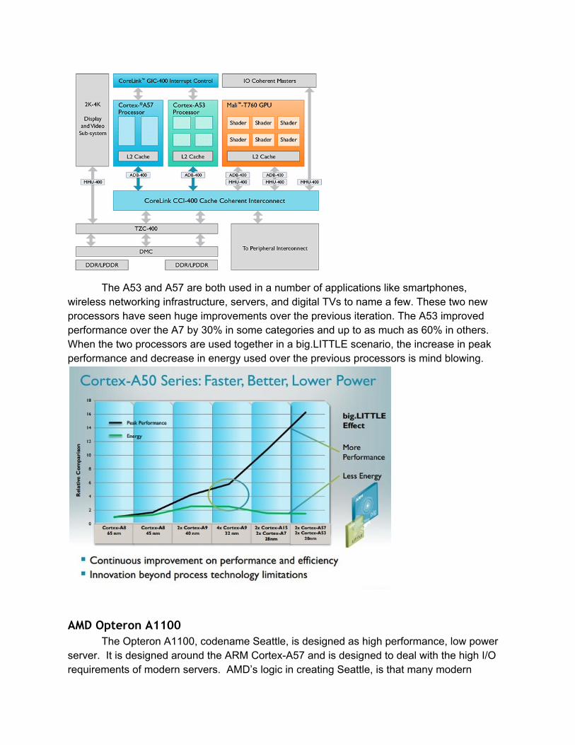
How exactly is switching processes done? This is from the CoreLink Cache Coherent Interconnect (CCI400). The CCI400 is a high performance, power efficient interconnect designed to interface between processors and the dynamic memory controller.The CCI400 design minimizes latency to ensure the maximum performance of latencysensitive processors.
The A53 and A57 are both used in a number of applications like smartphones,
wireless networking infrastructure, servers, and digital TVs to name a few. These two new processors have seen huge improvements over the previous iteration. The A53 improved performance over the A7 by 30% in some categories and up to as much as 60% in others. When the two processors are used together in a big.LITTLE scenario, the increase in peak performance and decrease in energy used over the previous processors is mind blowing.
AMD Opteron A1100 The Opteron A1100, codename Seattle, is designed as high performance, low power
server. It is designed around the ARM CortexA57 and is designed to deal with the high I/O requirements of modern servers. AMD’s logic in creating Seattle, is that many modern

applications have lower processing requirements than they do I/O requirements. This means that a new server can use more efficient, lower power, cores instead of expensive high performance processors.
The heart of the Opteron A1100 is eight CortexA57 cores. These are arranged in pairs sharing a 1MB L2 cache. All four sets of pairs share a common 8MB L3 cache. In addition to these main cores, Opteron A1100 also contains a single CortexA5 which acts as a controller. This tiny processor is used to control power usage, boot the system, and allow an administrator to configure the system. The final chip in the server is the Cryptographic Coprocessor (CCP). Although each CortexA57 already includes instructions for cryptographic operations, the designers felt that it would be helpful to offload some work. An example of this would be to use the built in instructions to handle simple tasks such as HTTPS, but use the CCP to handle compression and encryption of larger files.
Given the lowpower nature of ARM processors, there are fears about how the A1100 will stack up compared to other, more powerful processors. The following graph shows the results of running the SPEC CPU2006 int rate benchmark. While it looks like the A1100 is underpowered compared to its competition, it really shines when we look a power usage. The Xeon E31230L v3 1.8 needs 40W to achieve this performance and the XGene 1 2.4 needs 60W. The A1100, on the other hand, only needs 25W. Additionally, this benchmark tends to overemphasize core count as compared with other factors. The basic way this benchmark works is to run one instance of the process on each core of the machine. Because of this, no weight is given to a server’s ability to balance loads and deal with choked resources, something that the A1100 has been hinted to excel at. Ultimately, the benchmark doesn’t tell us too much that we don’t already know. The A1100 will not be able to compete head to head with many of the powerful servers and instead will have to find more niche markets. Unfortunately, we will not know the true performance until something more than a development board is released.

References: http://pc.watch.impress.co.jp/video/pcw/docs/614/543/08p.pdf http://www.anandtech.com/show/6420/armscortexa57andcortexa53thefirst64bitarmv8cpucores http://infocenter.arm.com/help/topic/com.arm.doc.uan0015a/cortex_a57_software_optimisation_guide_external.pdf http://community.arm.com/groups/processors/blog/2013/11/19/awalkthroughthecortexamobileroadmap http://community.arm.com/groups/processors/blog/2013/06/18/tenthingstoknowaboutbiglittle Computer Architecture A Quantitative Approach (5th edition) by Hennesy and Patterson ARM® Cortex®A57 MPCore Processor Technical Reference Manual Revision: r1p3 published by ARM