application of s-parameter techniques to amplifier design
TRANSCRIPT

Rochester Institute of TechnologyRIT Scholar Works
Theses Thesis/Dissertation Collections
1969
Application of S-parameter techniques to amplifierdesignFrank Sulak
Follow this and additional works at: http://scholarworks.rit.edu/theses
This Thesis is brought to you for free and open access by the Thesis/Dissertation Collections at RIT Scholar Works. It has been accepted for inclusionin Theses by an authorized administrator of RIT Scholar Works. For more information, please contact [email protected].
Recommended CitationSulak, Frank, "Application of S-parameter techniques to amplifier design" (1969). Thesis. Rochester Institute of Technology. Accessedfrom

Approved by:
APPLICATION OF S-PARAMETER
TECHNIQUES TO AMPLIFIER DESIGN
by
Frank Sulak
A Thesis Submitted
in
Partial FuJ.f'illment
of the
Requirements for the Degree of
MAsrER OF SCIENCE
in
Electrical Engineering
Prof. Name Illegible (Thesis Advisor)
Prof. K. W. Kimpton
Prof. G. W. Reed
Prof. W. F. Walker (Department Head)
DEPARTMENT OF ELECTRICAL ENGINEERING
COLLEGE OF APPLIED SCIENCE
ROCHEsrER INsrITUTE OF TECHNOLOGY
ROCHESTER, NEW YORK
MAY, 1969

Table of Contents
List of Tables I
List of Figures II
List of Symbols III
I Abstract IV
II Introduction 1
III Scattering Parameter Theory 2
IV Measurement of S Parameters 8
V Design Case #1 17
Design Case #2 21
Design Case #3 26
VI Conclusions 32
VII References 3^
Appendix I: Microstrip Line 35
Appendix II: Computer Program 39
4 4 '* ''S'.'
\-i
1 1 6 A -J (

List of Tables
Table # Contents
1 Measured S-Parameter Data lk
2 S-Parameter Design Equations 15-l6
3 Microstrip Parameter Equations 37
k Computer Output Data 45-48

List of Figures
Figure # ^tge
1 Two Port Model. 8
2 S-parameter Test Jig. 10
3 S-parameter Test Setup. 11
k Immittance Chart for Design Case #1. 18
5 Experimental Results of Design Case #1. 20
6 Immittance Chart for Design Case #2. 22
7 Experimental Results of Design Case #2. 25
8 Immittance Chart for Design Case #3. 28
9 Stripline Amplifier. 30
10 Experimental Results of Design Case #3- 31
11 z vs.q and z ,
vs. W/h graphs. 38ol ol
II

List of Symbols
s, . Scattering parameters.
K - Rollett's Stability factor.
r - The center of constant gain circle on the input plane.
ol
R - The radius of constant gain circle on the Input plane.
ol
r - The center of constant gain circle on the output plane.
o2
R The radius of constant gain circle on the output plane.
o2
r The center of stability circle on input plane.
si
R The radius of stability circle on input plane.
si
r The center of stability circle on output plane.
s2
R - The radius of stability circle on output plane.
s2
G - Maximum power gain possible.
max
R - Reflection coefficient of that source impedance required to
ms
conjugately match the input of the transistor.
R - Reflection coefficient of that load impedance required to
ml
conjugately match the output of the transistor.
G - Transducer power gain.T
G - Desired total amplifier gain (numeric).P
III

I Abstract
1. Discussion of s parameters and their applicability to high
frequency design.
2. Measurement of s parameters and evaluation of stable
operating regions.
3. Synthesis of high frequency transistor circuitry with the aid
of scattering parameter design equations.
4. Verification of design theory by evaluating the performance of
bread-board models.
IV
II Introduction
Improved high frequency performance of semiconductor devices has
made their use practical into the microwave frequency range. The
measurement of commonly accepted amplifier design parameters, such as
y, h or z parameters, becomes difficult over 100 MHz due to short and
open circuit port termination requirements. Since the scattering, or
s parameters, are related to the traveling waves on a transmission
line and their measurement can be referenced to the characteristic
impedance of the line, their practicality quickly becomes evident to a
designer.
Another one of the major advantages is that the matching networks
are also measured in terms of s parameters. Thus, once the scattering
parameters of both the active and passive circuits are determined, the
design of circuitry can proceed in a simplified manner.

Ill Scattering Parameter Theory
The interest of this author lies in two port amplifier design.
Thus, after a brief introduction to n-port scattering matrices, the
remaining discussion will be confined to two-port devices only.
Consider the n-port device
where the incident and reflected power waves are defined as
Vi*
Vi
P ReZj I
vi-
Vi1
^ReZj
Vj, and 1^ are the voltage and current respectively entering the i-th
port, whereas Z i is the impedance seen by the i-th port.
Using Kurokawa's simpler notation throughout the discussion of
n-port devices, the power wave vectors can be written:

a - F (v + Gi)
b - F (v - G+i)
Where F and G are diagonal matrices with 1/2 1| jRe Zif. and Zi being the
i-th component respectively, the + sign designates a complex transpose
matrix.
Since a and b are linear transformations of v and i, and since
v - Zi
there must be a linear relation between a and b. This is expressed by
Kurokawa as
b sa
Now using these relations, the generalized form of scattering matrix can
be found. Eliminating a, b, and v from
a - F (v + Gi) and
b F (v - G*i) we have
F (Z + G)i - SF (Z - G+)i
which can be arranged as
S - F (Z + G) (Z -
F~'
after dropping i and post multiplying both sides by (Z - G+) and F. In
practical design one must consider the behavior of the circuit with any
arbitrary source and load impedances. This is equivalent to replacing
all Zt's seen by the n-port with arbitrary impedances Zi's, keeping in

mind that there will be a reflection coefficient given as
(zj- z )
T m.
1 . *.
(zi+
zp
As Kurokawa has shown the new set of scattering parameters for this
case are
-
A"1
(S -r+) (IA+
where V and A are diagonal matrices with r and (l - r )
being their i-th diagonal components.
1 - r,
1- r,
When one substitutes the appropriate values, the tvo port s
parameters can be derived in the following manner:
ij
A -
(1 -
** 2gl> *-
ri
1 - r.
Sll S12
S21 S22
*v 2<l-g2> l' r2
1 - r.
r -
au
ri
*22
rs -
Sllrl S12rl
S2lr2 S22r2
A'1-l
*11 a22
a22
'11

(s - r+)
(su- rx> s12
s21 (S22" r2>
bll b12
b21 b22
(1 -
(1 - Vll)(l - r2s22) - r1r2s12s21
(1 *
r2S22) riS12
"
r2S21(X "
Vii
(1 - C
Cll C12
LC21 C22J
S -
all a22
a22
0 a11
bll b12
b-, b__21 22
Cll C12
C21 C22
*
all
0 a22
Performing the multiplication we have
alla22
a!la22(bllCll+b12C21) a22a22<bllCl2+b12C22)
allail(b21Cll+b22C21>a22all(b21C12+b22C22)
Substituting the appropriate values for the constants
Sll s12
S21 s22
Where

11
ll (sll"rl)(1"r2S22)+r2S12321
all(1 " riSll)(1 " V22) "
rlVl2S21
822S12
s12(l -
r, <)
all(1 " Vii)(1 " V22} "
V2S12S21
b21a
s21(l -
r2 *>
22 (1 - rlSn)(l - r2s22) - r1r2s12s21
22
a*2 (s22- r*)(l rlSu) ?
r^^
a22 (1 - Vll)(l - r2s22) - rir2s12s21
The behavior of a circuit for arbitrary load and source impedances
is indicated by the s equations. Prevention of oscillation is of
great importance in amplifier design. Depending on their ability to
resist oscillation, amplifiers are generally separated into two distinct
categories: the absolutely stable case, and the potentially unstable
case. An amplifier is absolutely stable if all passive source and load
impedances will insure oscillation free operation. A conditionally
stable amplifier is likely to oscillate if the load and source impedances
are not selected with particular care.
Examining the generalized scattering parameter equations of s
and s one can gain insight into the different cases of stability
since an oscillation free device has to satisfy the conditions:
<1t
s11<l
and
i
s22
Hence, the design equations concerning circuit stability are derived
from s., and s22. A two port, for example, can be conjugately matched
t i
simultaneously at both ports if s.,- 0 and
s22- 0 can be satisfied with
a given set of load and generator impedances.
The references given should be consulted for detailed discussion of
two port network stability.
The stability and the design equations are expressed in terms of
the s.. device parameters. Thus, the first step in amplifier design
consists of the evaluation of scattering parameters of a selected semi
conductor.
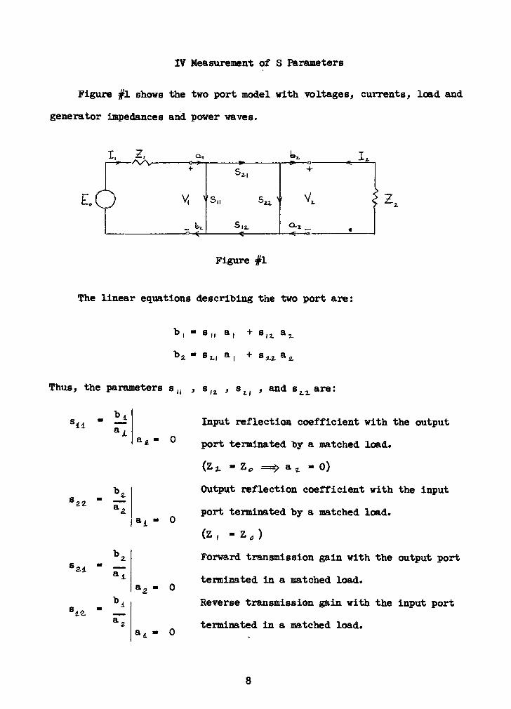
IV Measurement of S Parameters
Figure #1 shows the two port model with voltages, currents, load and
generator impedances and power waves.
I, Z,-4. A/V-
E.6
a.,-o->-
V vs
_ ko ^_
S12.<
-3.o-
s v Vt
a.1 _
Figure #1
The linear equations describing the two port are:
b,-
s a, + aiz at
ba atl a,+sua4
Thus, the parameters s(( , s,2 , si( , and s^are:
b
'il
a- - 0
zz
a4- 0
'2d
*a
a4- 0
Input reflection coefficient with the output
port terminated by a matched load.
(Zt -Ze => ax- 0)
Output reflection coefficient with the input
port terminated by a matched load.
(Z,- Z
c )
Forward transmission gain with the output port
terminated in a matched load.
Reverse transmission gain with the input port
terminated in a matched load.

The s . parameters of a semiconductor thus can be determined over
the desired frequency range on the broad band basis using a 50 ohm
system. These measurements can be performed in a reasonably simple
manner with the use of a carefully constructed test jig. Since the
reflection and transmission coefficients of a transistor are to be
measured with respect to a 50 ohm system, the construction of three
identical lines on the same board is helpful. (See Figure #2)
Line A is straight through 50 ohms reference transmission line.
(See Appendix I for a calculation of line width) Line B is short
circuited at the center of the board. Transmission line C is cut at
the center and appropriately modified to serve as a mount for the de
vice to be measured.
A block diagram showing an s parameter test set up is Illustrated
in Figure #3.
The basic procedure to determine s and s. is to measure the
magnitude and the phase angle of the incident and reflected voltages.
The value ofs-2
and s2, is determined by measuring the magnitude and
the phase angle of the incident and the transmitted voltages. For the
s., and s . measurements, the system is calibrated with the shorted
section. The reflected wave at the short circuit is
Vref1." "
incident since
2L - Z
p - 6k atld z. - 0
ZL+Zo

/ /1/ / / / / / / / /
CE A 50 JTi. THROUGH LINE n
/ / / / ////// /CZ 6 SOSl SHORTED LINE 50XI .SHORTED LINE =D
//
/
/ //////// /
C= C Son BASE LINE so oC 50SI. COLECTOH LIMB 3
/ / E / #V / / / /SM5 /A/pr
-^GROUKID PLANE
a) S-parameter test jig for TO-5 transistor can
/
(O)8 ) C
7 / / /AWTT/
b) S-parameter test jig for strip-line transistor
Figure #2a and 2b
10

4
0 -O
n >
C^
-*>
"O
p
I-
o
>
o-
0 f
V
_d
ri
5
F"
nQ
IU v>b-. ui 3 m %-4
o 3: 5<n -4 K-J ,k *>
LJ IJ U
-J
o
c
? o
<nJ
5
4
0
ho
Uj
QCor
uj
-a
d
0
Cj
LJ
cjJ i
-1 Ul o
< o ^
z 6:
Ci. 3
o
<4) v>
11

The reflected voltage wave measured with the B channel of the vector
voltmeter will be in the form
V - - V xe^s
refl. incident
This phase delay of ps is due to the additional path length that the
reflected signal must travel. Thus, inserting a line stretcher in the
path of the incident wave a delay can be introduced which will compen
sate for the path difference. Placing the transistor in the line and
adjusting the signal source to register a unity reading on channel A
gives the magnitude and phase of s reflection coefficient on channel
B.
The output reflection coefficient s2can be measured with the same
test setup when the transistor jig is reversed, i.e. the output becomes
the input and vice versa.
For the measurement of the forward and the reverse transducer gains
s.. and s , the test setup can be calibrated with the through trans
mission line section of the jig when probe B is in B. position. The
line stretcher is utilized in the path of the incident wave to compen
sate for the phase delay of the transmitted wave. After the phase com
pensation, s.. can be measured when the transistor jig is inserted into
the signal path. If the signal source is set to register unity reading
on channel A, the magnitude and phase of s can be read directly on
channel B.
The reverse parameter s _ is measured by exchanging the input and
output ports of the transistor jig.
12
The above outlined technique was employed in the evaluation of some
semiconductor devices in the 100 MHz to 400 MHz range. System cali
bration was done in the middle of the frequency band for both reflected
and transmitted waves. This method yielded better than 5 phase ac
curacy throughout the measured frequency band. Experimental data is
listed in Table #1.
Knowing the s. . parameters of a transistor at the desired operat
ing level, one can proceed with the evaluation of the design equations
and obtain stability, transducer gain, and matching condition infor
mation. (See Table #2) Since these design equations are algebraic
combinations of vector quantities, their manual evaluation could be
unenlightening and lengthy. To avoid these calculations, a computer
program was developed as a design aid. See Appendix #11 for the pro
gram. This program accepts s parameter data in vector form as they are
read from the vector voltmeter. The computer output data is listed in
Table #4.
The following design examples are based on the evaluated s param
eter data and the applicable computer output data.
13

TABLE #1 Measured S-Parameter Data
Transistor : 2H3866 Bias: vCE- 24v Ie- 50ma
Freq. MHz. s|/a
8. /B,z. k.l /st/ Is1 2-2 1 S.
100.265 -160 .05 82 7.8 90 50 -17
150 .260 -170 .07 82 5.0 80 .50 -20
200.255 -176 .09 82 3.8 73 51 -23
250 .245 178 .11 80 3.2 68'
-53 -26
300 .2k 170 .13 80 2.7 60 56 -30
350 .2k 163 .15 80 2.35 52 58 -33
400 .2k 15* .18 78 1.95 k& .60 -35
Transistor : 2N4429 Bias: vCE- 24v 1e- 50ma
260 7 -180 .03 80 2.8 75 57 -28
350 7 163 .Ok 83 2.55 62 .58 -34
400 71 158 .05 84 2.25 55 58 -38
500 75 150 .07 86 1.75 45 59 -43
14

Table #2 S-Parameter Design Equations
A SliS22"
S12S21
K
B.
B
lsul2-ls22|
2lS12S2li
-l*|su|2-|s22|2-|A|2
-1+lS22|2"lSll|2"lA|2
"
S11"AS22
S22"Astl
max
R_ms
ml
'21
s(K -tK - 1 ) If B 0 then the + sign applies
- C
12
2 C,
B2 :$6 4 C
2 C,
If B and B_ are negative, then
the + signs apply.
11
I2
U22l2
" Is21
VGt
si Cl/Dl
si S12S21 l/Dl
15

s2 C2/D2
Rs2 S12S2ll/D2
Loi
ol
1 +
Dt G
(1 + 2K|s12s21|G + | sl2s2J2xG2)%
1 +
Dj G
lo2
Rb2
1 +
D2 G
(1 + 2K|sl2s21|G + |s12s21|2*G2)*
1 +
D2G
16

Design Case #1
A driver amplifier is required for the 170 MHz to 190 MHz fre
quency range. From the computer output data listed in Table #4, the
2N3866 should provide an absolutely stable operation at 200 MHz (K>
1) with a maximum gain of 14.8 db when both input and output are con-
jugately matched. To achieve conjugate match at both input and output,
we need
R -.736
/178.9
ms
*1-.819 /
23.9
By plotting these reflection coefficients on an Immittance Chart, one
can obtain the required impedances directly from Figure #4.
Z * 8 ohmss
Z. - (100 + j 190) ohms
Assuming that the amplifier is driving a 50 ohms load and is being
driven by a 50 ohms source at the same time, we need matching networks
to transform 50 ohms to R and R . to 50 ohms. Since shunt susept-
ms ml
ances or series reactances move along constant admittance or constant
impedance circles respectively, an L section will match R . to 50 ohms.
From Figure #4.
1X -
,. 82 ohms
12 x10"J
1 70 nhy
X n- 140 ohms
C2
C2- 5.5 pf
17

TITLE Figure // 4
\fAU YTANCE CHA^
t:ATE
FOR 2192 IMPEDANCE COORDIN/ 'ES 50 OHM CHARACTERI'
'C IMPEDAIiCE
ADMITTANCE COORDINATES 2(3 MILLIMHO CHARACTERISTICADMI'
TANCE
I 4"
IS _J I 1 ll. 1 L_L_J__1 1_
O 00 it *$
._Ii ; i i 7 i i L
TOWARO GENERATOR -
m oo os?
2i8 g
+H'(-V-H-!rfr'- <i i
'I
o o q Q
v'tt VOL 17. NO. I. FP.-I10-I5S. JI8-J2S. JAM. 194*
RADIALLY SCALED PARAMETERS .
pfa o 8 S i S S'I" H-V-'-W-'.
'
.'
1'i'i' ' 1 ' 'i' '' 'i' ''-
H^1-1
bbooo- to g*
-
i\> & o <a o o o
oyio x. p o o fc> O O O
r-H-H~4'', ', ',' 'i'iVi'i' ' I1 l'
i'i' '
*-?
II '
|' 4-Mt+ttttt
i TOWARD LOAD
-T . 'lI1 V
CENTER
&'. . nytl (Mi fcv
fELECTPDNICSOIVI9IO*

The input matching can be accomplished with a bifilar wound im
pedance transformer and a small capacitance in series with the base to
tune out the slight amount of inductance introduced by the transformer
winding. The final configuration shown below illustrates the complete
circuit.
p +2-S
>e-
50 n.
r,
cu
i*
-M- C44
6 1
in
r"
5~o_CL
Rt- 3.6 KEl
R2- 560X2.
R3- 100X1
T, - 4 turns bifilar
C. -
C -
C, -
5 - 25 pf
.8- 10 pf
1000 pf
1000pf
L2- 70 nhy
Amplifier performance is illustrated in Figure #5.
If other than maximum gain is required, one can construct constant
gain circles and design appropriate matching networks that match source
and load to a given gain circle.
19

fl)
r
aCO
9cr
60Q
Ol
Cl
CO
c
ib
u5
HV
CO
q in o
20

Design Case #2
A medium power amplifier is required in the 340 MHz to 390 MHz fre
quency range. The low priced 2N3866 was investigated again for possible
application.
S parameter data and the computer output data from tables 1 and 4
respectively indicate the following:
K<1
Therefore, G^^ is undefined; i.e. simultaneous complex conjugate match
ing at both input and output ports would require R
potentially unstable regions are:
I .
- 25.08 r,
si siR .
- 25.08 r,- 25.97
/-158
Rs2m 31,,33
Rslm 22,,72
Rs2m 17,,33
RslB3 45.,68
RS2- 10.,88
rs2" 57,95
/"145
r .
- 23.66/-164
si i
rg2- 31.61
/-147
rsl" 46,63
/"170
rg2- 18.66
/-150
t .
- 1.ml
T
@ 400 MHz
@ 400 M
@ 350 II
@ 350 II
@ 300 I
<a 300 I
Figure #6 shows the unstable regions which occur on the input plane only.
To achieve approximately 15 db amplifier gain between 50 ohms
source and 50 ohms load, an attempt was made to match all impedances as
nearly as possible tos^ of the appropriate stage.
21

TITLE Fl f-Eur c 3- 6DATE
FORM 2192
IMMITTANCE CHART
IMPEDANCE COORDINA ES j OHM CHAR/ ER! 'C IMP. ANCE
ADMITTANCE COORDINATES 20 MILLIMHO'
iARACTERISTIC ADMITTANCE
Cl-
VOL 17, NO. I, PP-IJO-IJJ, 318-325, JAN 194. EL I CTRDNIca rjl\': '.ID rj

Amplifier configuration is shown below.
-)
-nnr>
looo f>F
3^
V3-G.K
"TtT
I
,+2
Iooo fxF
3.6K
ZM3&GG
Pf
6' i 6-1i
C, .8-IOpF
66 y-^x
Ho > J_ looopF
loo
^seo >
3<SGC
looo pF
XI
Matching networks can be determined from Figure #6 in the following
manner:
L117 x
IO"3
23 nhy
15 ohms
57 ohms
vcl
Cj- 30 pf
*L2-
18 x 10
L2- 22 nhy
X -
- 62 ohms
rs- 55 ohms
2
*L3'
7 pf
1
15 x 10
_- 67 ohms
-3
L3- 26 nhy
X ,- 80 ohms
C,- 5 pf
23

The circuit was bread-hoarded and tested with the indicated values.
Amplifier performance is shown in Figure #7.
Although a single stage 2N3866 amplifier @ 400 MHz did oscillate as
was anticipated when being tuned at both ports, the two stage amplifier
did not show oscillation any place in the range of tuning elements. This
indicates that the s;,' parameters of the composite stage must have satis
fied the following condition:
ISilUl
24

/
<--
33
>?
3
0
"ti
c
~x
~5
"0
o
a*
o
o-1
t-
o <3
0)aa
I(0
a)
OS
8cr
H
IM
o>*
<<)
s60rl
fr*
o
*"4
<0
25

Design Case #3
This example is intended to illustrate the utilization of strip-
line techniques in the design of high frequency amplifiers. S param
eter data is listed in Table #1 for the 2N4429 transistor which is op
erated with a dc grounded emitter. The grounded emitter operation
(R - 0) would result in thermal instability, however, this is compen
sated for with the pnp transistor and the zener diode in the biasing
stage.
The list of the computer output in Table #4 contains the desired
design information. It was determined by using tuning stubs and s pa
rameter techniques that the amplifier will yield the desired response,
illustrated in Figure #10, with the following impedance conditions:
Frequency Reflection coefficient presented
at the input ps
350 MHz ps - .56
/-164
400 "ps - .56 /
175
at the output p1
pi - .48 /36
pi - .38 /28
The strip- line matching-element values which will transform the load
and source impedances to the above indicated reflection coefficients can
now be determined. Depending on the designer's preference, these values
can be calculated from the appropriate design equations, or they can be
determined by graphical techniques.
26

Since the mathematical approach is illustrated in the sighted refer
ences , graphical methods will be utilized in this paper.
Output matching.
Vfe want to match the transistor output impedance of 90 + j38 ohms (See
Figure #8) at 400 MHz to a 50 ohm load impedance. A shorted inductive
stub parallel with the load will transform the load on the 20 mmho line.
The intersection of the constant SWR circle, drawn through the source im
pedance point on the immittance chart, and the 20 mmho admittance circle
determines the proper value of the shunt stub. (See Figure #8) The
value of the stub should be j 17 mmhos. Starting from the shorted end
of the admittance chart, it can be seen that the required stub length
is 0.138 of a wavelength. Since
. 300 xIO6
m/secA rs
75 '* and er" 2-16
400 x106
^/sec * R
A(ER) - 51 cm
Therefore
Lshunt
" 7a
This new load admittance can be transformed to the source impedance on
the constant SWR circle with a 50 ohm transmission line. The proper
length of this line is
L (0.211 - 0.094) A (^
-.117 x 51 6 cm
27

TITLE Figure #8
IMMITTANCE CHART
DATE
FORM 2192 IMPEDANCE COORDINATES - 50 OHM HAR rERIS IC IMPEDANCE
ADMITTAf-XE COORDINATES- 20 MILLIMHO CH RACTERISTIC ADMITTANCE
Kticua,uc$-
VOL 17, NO. I,Pp.- 130
-
133, 318 -324, JAN 1944 tl-ECTRONlCB DIVIDIOrvJ

Input Matching.
We want to match the 50 ohm source impedance to the 14 + j2 ohms tran
sistor input impedance at 400 MHz. A capacitive parallel stub is chosen
to transform the source impedance clockwise on the 20 mmho line. The
intersection of the 20 mmho line and the constant SWR circle, drawn
through the 14 + j2 ohms point, indicates that the required capacitive
susceptance is + j27 mmhos.
Therefore, the length of the open end stub is
Vallel-<0-398"0-250>A<V
- 7.58 cm
The required length of the series 50 ohm transmission line is
Lseries' (0'078 + '7^ (V
- 0.085 x 51 - 4.33 cm
The complete circuit is shown in Figure #9.
The circuit was bread-boarded on a 1/32 inch single-sided teflon
board. The strip- line was constructed using adhesive copper tape cut
to the proper dimensions. Amplifier performance is illustrated in
Figure #10.
29

0?
o 1|.
ir
es)
cs!
>-L
0 ri\.r\ I
o
U3
o
m
rO
-aaa-
OO
-0
a.
Cl
0
*f
W)
2 HHHhHN
<VW-
\
u.
Q.
0
0
o
0
~T oj
*6
c!3C
eg
o
A>
ri
CO fl)
Cvjrl
rl
+ r-l
s
Io.t4
rl
4J
ON
0)
60
c>
O ^:
30

-e
oi -!r
ifcl
fl)(0
!(0
fl)
tn
>>
1cr
fl>
u
n
U4
ol
O
Ol)
s
I
O.
rl
cn
o1-4
4)
IH
*J
.5*>
o
r-!
O
o
O
cr
31

VI Conclusions
The accuracy of measured s parameters is influenced by several
factors since their measurements are based on the evaluation of inci
dent and reflected voltage waves. In view of this, the existence of
multiple reflections, due to mismatches in the path of the signal,
should be avoided in the test set-up. This problem was minimized by
the employment of low VSWR bias elements, tee's, connectors, and loads.
The directivity and the coupling factor of the dual-directional couplers
also influence the measurement accuracy; however, if required, a cali
bration curve can be made up for the system.
The uniformity and the accuracy of the 50 ohm lines on the test
jig, the proper grounding of the shorted reference line, and the quality
of the RF connections will also affect s parameter data accuracy. These
experimental errors were minimized with the careful construction of the
transistor test jigs. With all these influencing factors minimized,
measurement accuracies can be held well within engineering design re
quirements. This is evident from the close correlation of the theoret
ical and experimental results.
In Design Case #1, a maximum gain of 14.8 db was predicted at 200
MHz. Experimental results yielded 14.6 db at 187 MHz, but response
could be tuned to peak at 200 MHz.
G is undefined for Design Case #2 because K<1. One could pre-
maxK
diet approximately 8 db gain per stage at 400 MHz on the basis of design
equations, a two stage bread-board model yielded 17.2 db at 400 MHz.
32

Theoretical and experimental values agree to within 1 db for Design
Case #3 with 12 db being the desired gain and 12.8 db the obtained gain
at 363 MHz.
The understanding and utilization of s parameter design techniques
can lead to predictable and efficient amplifier design. Their impor
tance cannot be over emphasized, and s parameter design techniques
should be given equal value with those utilizing y parameters (as de
scribed by Linvill ). As semiconductor devices are making their way
into higher frequency ranges, the work of a designer is being somewhat
lessened since data sheets for these devices are now appearing with
both s and y parameter values . This also indicates the rapid rate of
recognition that s parameters are gaining amongst design engineers.
33
VII References
1. K. Kurokawa, "Power Waves and the ScatteringMatrix," IEEE Trans
actions on Microwave Theory and Techniques, Vol. MTT-13 No. 2,
March, 1965.
2. G. Boadway, "Two Port Power Flow Analysis Using Generalized
ScatteringParameters," Microwave Journal, Vol. 10, No. 6, May,
1967.
3. J. Lange, "Microwave Transistor Characterization Including S-Pa-
rameters" Hewlett-Packard Application Note No. 95.
4. R. W. Anderson, "S-Parameter Techniques for Faster, More Accurate
Network Design," Hewlett-Packard Journal, Vol. 18, November 6,
February, 1967.
5. W. Froehner, "Quick Amplifier Design with ScatteringParameters,"
Electronics, October 16, 1967.
6. A. Presser, "RF Properties of MicrostripLine,"
Microwaves, March
1969.
7. J. Linvill and J. Gibbons, "Transistors and Active Circuit,"
McGraw-Hill, Inc., New York, 1961.
8. Fairchild Semiconductor, "S Parameters for Microwave Transistors."
9. J. A. Kuecken, "Antennas and Transmission Lines," General Dynamics
Electronics Division.
34

Appendix I
The characteristic impedance of a microstrip transmission line,
which has a single ground plane, can be calculated by an iterative
gtechnique . Table #3 lists the microstrip parameter equations. The
cross-sectional view with dimensions is indicated in the figure below,
-W-r\I I -L-i
T
R ( 3D i e, I e. c t r i c]
G-roand Plcxrie.
The design steps are as follows:
1. The line is assumed to be completely embedded in a dielectric sub
strate with dielectric constant E . The free-space impedance is
then
Z .- [eTz
ol ' R o
2. The filling fraction q is determined from Z - vs. q graph. (Figure
#11)
3. The effective dielectric constant is calculated from
E^- 1 + q (E^
- 1)
4. Zq1is recalculated with
ER replacing E^ Steps 2 through 4 are
t
repeated until ER in Step 3 is within 17. of the previous value.
5. The shape ratio /fc is read from Z . vs. /. plot.
35

For a teflon board, where 6^= 2.6 and the desired
Z0 50 ohms, the calculations proceed:
lm Zol-f^Zo-80'5
2.q-.705
3- E^-l+qCEj-1)- 2.13
la) Z .- 1.46 x 50 - 73
01
2a) q-.725
1
3a) E - 1 + .725 (2.6 - 1) - 2.16R
lb) z - 73.501
2b) q-.72
3b) ER- 2.15
The shape ratio from Z0, vs. ^^ graph is 2.8 making the width of
the 50 ohm line 0.176".
The microstrip lines of the test jig were constructed in accordance
with these calculations by etching technique and were measured to be
50 - 2 ohms on a Time Delay Refleetometer.
36

Table #3 -- Microstrip Parameter Equations
zolCharacteristic Z pp*
Relative effective
dielectric constant
Relative dielectric con
stant of substrate
Effective dielectric
constant
-o {yimpedance (ohms)
' R
E;- 1 + q (ER
- 1)
Guide wavelength
Free-space character- -
istic impedances (ohms)
K-K'\
ol
ER
Filling fraction q
Free-space wavelength A
t
ER
37

Figure # 11
So too >5 2.
Free-space impedance (ZQ,) - ohms
z50
38

Appendix II
Convert l Decree,
to f^o-ol <ixx,rt S,Vol<xr tore.tzt a-n
qul<3-r"
Coo r-ol in ixtts-
Compute: A,K, Ci,CZ,Bi,BZ,
T>1,D2-
k.
Compute; GT
P'mismatch INPUT,
^MISMATCH 0UTPU1
\/
Compute;
rsi) Ksi
V
39

V \<
Compute :
G"max,Rms
Computet
G"max,Rms
r\
C o rr, pwt e :G-M/U-P
Convert: R^s*"
Rml to pola.r
0oor-d in art e-&
Write: K,
^MouTPiJ-r,
\G-m*x,Rms/
CLE4R;-
Scj matrix
Convert :
"St, rsz
To polar
coo roHmxtes
.
,
Write; K^Gy/
Fm input.
^m output!
Compute,;
R,ML
NX/RITE:
"5J, Rsi,R,Si,
40

C AMPLIFIER DESIGN WITH S-PARAMETERS
C A(l) AND AA(l) ARE THE MAGNITUDE AND PHASE ANGLE OF S(l,j)
C WHERE 0)A(I))1 -180)AA(I))180
DIMENSION A(l0),AA(l0),BR(l0),S(20)
REAL A,M,BR,AK,B1,B2,D1,E2,RS1,RS2,FREQ,GMAX,HMS,RMSA,RML,
1RMLA,GT,IM1,BG
COMPLEX S,DEL,C1,C2,CRS1,CRS2,RIN,R0T
100 READ(5,101) FREQ, (A(l),AA(l),1-1,4)
101 FQRMAT(F16.3,8F7.3)
WRITE (6, 102) FREQ
102 FORMAT (IX,1 FREQUENCY - SFIO.O,'MHZ*)
PI - 3.14159265
DO 105 I - 1,4
BR(I) - 0.0
S(I) - CMPLX(0.0,0.0)
BR(I) - AA(I) * (PI/180.0)
S(I)-CMPLX(A(I)*COS(BR(I)),A(I)*SIN(BR(I)))
105 CONTINUE
C COMPUTE ALL NECESSARY VARIABLES
DEL-S (1)*S (4)-S (2)*S (3)
AK-(1.0+(CABS(DEL))**2-(CABS(S(l)))**2-(CABS(S(4)))**2)/(2.0*
1CABS(S(2)*S(3)))
C1-S(1)-DEL*C0NJG(S(4))
C2-S (4)-DEL*C0NJG(S (1) )
41

B1-1.0+(CABS(S(1)))**2-(CABS(S(4)))**2-(CABS(DEL))**2
B2-1.0+ (CABS (S ($ ) ) )**2- (CABS (S (1) ) )**2- (CABS (DEL) )**2
D1-(CABS (S (1) ))**2- (CABS (DEL))**2
D2- (CABS (S (2) ) )**2- (CABS (DEL) )**2
GT-10.O*AL0G10 (CABS (S (3) )**2)
PM1-ABS (10.0*AL0G10(1.0-CABS (S (1) )**2))
PM2-ABS (10. 0*AL0G10 ( 1 . 0-CABS (S (2) )**2) )
IF(AK.LE.l.O) GO TO 160
IF(Bl.LT.O.O) GO TO 200
GMAX-CABS(S(3)/S(2))*(AK-SQRT(AK**2-1.0))
RIN-CONJG (Cl)* (Bl-SQRT (Bl**2-4. 0*CABS (C 1)**2) )/ (2 . 0*CABS (C1)**2)
GO TO 210
200 GMAX-CABS(S(3)/S(2))*(AK+SQRT(AK**2-1.0))
RIN-CONJG(Cl)* (Bl+SQRT(Bl**2-4. 0*CABS (C1)**2) )/ (2. 0*CABS (C1)**2)
210 CONTINUE
IF(B2.LT.0.0) GO TO 220
ROT-CONJG(C2)*(B2-SQRT(B2**2-4.0*CABS(C2)**2))/(2.0*CABS(C2)**2)
GO TO 230
220 ROT-CONJG(C2)*(B2+SQRT(B2**2-4.0*CABS(C2)**2))/(2.0*CABS(C2)**2)
230 CONTINUE
GMAX-10. 0*ALOG10 (GMAX)
RMS-CABS (RIN)
RMSA-57.29578*ATAN2(AIMAG(RIN),REAL(RIN))
RML-CABS(R0T)
RMLA-57. 29578*ATAN2(AIMAG(ROT) ,REAL(ROT))
42

WRITE (6,250) AK,GT,PM1,PM2
250 F0RMAT(1X, 'STABILITY FACTOR K- ,,lPEl4.5/ , TRANSDUCER GAIN -
1,1PE10.3, DB/*,MISMATCH LOSS INPUT -
',1PE10.3,' DB
2/, 'MISMATCH LOSS OUTPUT - ',1PE10.3, DB)
WRITE (6 ,450) GMAX,RMS,RMSA,RML,RMLA
450 F0RMAT(1X,GMAX - SIPEIO.S,' DB/' ',RMS
- ,1PE10.3,AT AN
1ANGLE OF ,lPE10.3/ ','RML - ,1PE10.3, AT AN ANGLE OF ',1PE10.
33)
151 DO 155 1-1,4
A(I)-0.0
AA(I)-0.0
155 CONTINUE
GO TO 100
160 CRS1C0NJG(C1)/D1
RSI-CABS (S (2)*S (3)/Dl)
CRS2-C0NJG(C2)/D2
RS2-CABS (S (2)*S (3) /D2)
C CALCULATE MAGNITUDE AND PHASE OF CRS1 AND CRS2
ARSl-CABS(CRSl)
PH1-57. 29578*ATAN2(AIMAG(CRS1) , REAL(CRSl) )
ARS2-CABS(CRS2)
PH2-57. 29578*ATAN2 (AIMAG(CRS2) , REAL(CRS2) )
WRITE(6,150) AK,GT,PM1,PM2
43

150 P0RMAT(1X,STABILITY FACTOR K- ,1PE14.5 / ,' TRANSDUCER GAIN
1',1PE10.3, DB'/'', 'MISMATCH LOSS INPUT - ',1PE10.3, DB'
2/'', 'MISMATCH LOSS OUTPUT - '.1PE10.3,'
DB')
VRITE(6,170) RS1,ARS1,PH1,RS2,ARS2,PH2
170 F0RMAT(1X,'RAD1 - ,1PE10.3," DIST1 - ',1PE10.3, AT AN ANGLE 0
IF MPE10.3/' ,RAD2 - '.1PE10.3,' DIST2 - ',1PE10.3, AT AN
2ANGLE OF '.1PE10.3)
GO TO 151
180 CONTINUE
STOP
END
44
Table #4
2N3866 Data Card Code 2N3866-11 17
FREQUENCY - 100. MHZ
STABILITY FACTOR K - 9.58951E-01
TRANSDUCER GAIN - 1.784E 01 DB
MISMATCH LOSS INPUT - 3.162E-01 DB
MISMATCH LOSS OUTPUT - 1.249E 00 DB
RAD1 - 1.93 IE 02 DIST1 - 1.940E 02 AT AN ANGLE OF 1.654E 02
RAD2 - 5.936E 00 DIST2 - 8.625E 00 AT AN ANGLE OF -1.610E 02
FREQUENCY - 150. MHZ
STABILITY FACTOR K - 1.04527E 00
TRANSDUCER GAIN - 1.398E 01 DB
MISMATCH LOSS INPUT - 3.040E-01 DB
MISMATCH LOSS OUTPUT - 1.249E 00 DB
GMAX - 1.724E 01 DB
RMS - 7.523E-01 AT AN ANGLE OF 1.738E 02
RML - 8.268E-01 AT AN ANGLE OF 2.130E 01
FREQUENCY - 200. MHZ
STABILITY FACTOR K - 1.05305E 00
TRANSDUCER GAIN - 1.160E 01 DB
MISMATCH LOSS INPUT - 2.920E-01 DB
MISMATCH LOSS OUTPUT - 1.308E 00 DB
GMAX - 1.485E 01 DB
45

RMS - 7.361E-01 AT AN ANGLE OF 1.789E 02
RML - 8.196E-01 AT AN ANGLE OF 2.393E 01
FREQUENCY - 250. MHZ
STABILITY FACTOR K - 1.00660E 00
TRANSDUCER GAIN - 1.010E 01 DB
MISMATCH LOSS INPUT - 2.688E-01 DB
MISMATCH LOSS OUTPUT - 1.432E 00 DB
GMAX - 1.414E 01 DB
RMS - 8.945E-01 AT AN ANGLE OF -1.759E 02
RML - 9.331E-01 AT AN ANGLE OF 2.659E 01
FREQUENCY - 300. MHZ
STABILITY FACTOR K - 9.49056E-01
TRANSDUCER GAIN - 8.787E 00 DB
MISMATCH LOSS INPUT - 2.576E-01 DB
MISMATCH LOSS OUTPUT - 1.634E 00 DB
RAD1 - 4.568E 01 DIST1 - 4.663E 01 AT AN ANGLE OF -1.700E 02
RAD2 - 1.088E 01 DIST2 - 1.866E 01 AT AN ANGLE OF -1.500E 02
FREQUENCY - 350. MHZ
STABILITY FACTOR K - 9.39729E-01
TRANSDUCER GAIN - 7.235E 00 DB
MISMATCH LOSS INPUT - 2.576E-01 DB
MISMATCH LOSS OUTPUT - 1.781E 00 DB
RAD1 - 2.272E 01 DIST1 - 2.366E 01 AT AN ANGLE OF -1.641E 02
RAD2 - 1.733E 01 DIST2 - 3.161E 01 AT AN ANGLE OF -1.473E 02
46
FREQUENCY - 400. MHZ
STABILITY FACTOR K - 8.91743E-01
TRANSDUCER GAIN - 5. 80 IE 00 DB
MISMATCH LOSS INPUT - 2.576E-01 DB
MISMATCH LOSS OUTPUT - 1.938E 00 DB
RAD1 - 2.508E 01 DIST1 - 2.597E 01 AT AN ANGLE OF -1.580E 02
RAD2 - 3.133E 01 DIST2 - 5.795E 01 AT AN ANGLE OF -1.459E 02
2N4429 Data Card Code 2N4429-50,...53
FREQUENCY - 260. MHZ
STABILITY FACTOR K - 1.69296E 00
TRANSDUCER GAIN - 8.943E 00 DB
MISMATCH LOSS INPUT - 2.924E 00 DB
MISMATCH LOSS OUTPUT - 3.910E-03 DB
GMAX - 1.484E 01 DB
RMS - 8.035E-01 AT AN ANGLE OF 1.797E 02
RML - 7.242E-01 AT AN ANGLE OF 2.750E 01
FREQUENCY - 350. MHZ
STABILITY FACTOR K - 1.31973E 00
TRANSDUCER GAIN - 8.131E 00 DB
MISMATCH LOSS INPUT - 2.924E 00 DB
MISMATCH LOSS OUTPUT - 6.954E-03 DB
GMAX - 1.466E 01 DB
RMS - 8.457E-01 AT AN ANGLE OF -1.648E 02
RML - 7.879E-01 AT AN ANGLE OF 3.09 IE 01
47

FREQUENCY - 400. MHZ
STABILITY FACTOR K - 1.12946E 00
TRANSDUCER GAIN - 7.044E 00 DB
MISMATCH LOSS INPUT - 3.046E 00 DB
MISMATCH LOSS OUTPUT - 1.087E-02 DB
GMAX - 1.435E 01 DB
RMS - 8.954E-01 AT AN ANGLE OF -1.603E 02
RML - 8.508E-01 AT AN ANGLE OF 3.390E 01
FREQUENCY - 500. MHZ
STABILITY FACTOR K - 8.21120E-01
TRANSDUCER GAIN - 4. 86 IE 00 DB
MISMATCH LOSS INPUT - 3.590E 00 DB
MISMATCH LOSS OUTPUT - 2.133E-02 DB
RAD1 - 2.718E-01 DIST1 - 1.233E 00 AT AN ANGLE OF -1.530E 02
RAD2 - 1.146E 00 DIST2 - 3.220E 00 AT AN ANGLE OF -1.432E 02
48