analysis of - nasa
TRANSCRIPT

1
N
ANALYSIS OF LIGHTNING lNDUCED N A ~ R C ~ A ~ ECTRICAL SY STE
by Paul T. Hacker Lewis Research Center Cleveland, Ohio
and
General Electric Company gh Voltage Laboratory itt sfield, Massachusetts
PER proposed for presentation at 1970 Lightning icity Conference sponsored by the Society of eers and the Ai r Force Avionics
ecember 9-

MEASUREMENTS AND ANALYSIS OF LIGHTNINGINDUCED VOLTAGES IN AIRCRAFT ELECTRICAL CIRCUITS
Paul T. Hacker Aerospace Safety Research and Data Institute
National Aeronautics and Space Administration Lewis Research Center
Cleveland. Ohio
and
J. A. Plumer General Electric Company High Voltage Laboratory Pittsfield Massachusetts
AB ST RACT 4 a m lc ,&
A ser ies of measurements were made of volt- ages induced in electrical circuits within a metallic aircraft wing by full-scale simulated lightning cur- rents flowing through its skin and structure. The measured data were mathematically analyzed to en- able determination of voltages across load imped- ances to which the circuits might be connected else- where in the aircraft. voltages and lightning current, wing structural and circuit parameters were determined. Induced volt- ages of magnitudes likely to cause damage o r inter- ference with avionics were measured.
Relationships between induced
LIGHTNING TO AIRCRAFT has been recognized as a hazard for a long time. The hazards to aircraft due to lightning strikes are manifested in several forms, such a s
(1) Damage to the aircraft structure. (a) Pitting and holes in metallic surfaces. (b) Delamination and loss of strength of com-
posite nonmetallic materials. (2) Ignite fuels vapors in tanks through
(a) Holes burned through or hot spots created
(b) Arcing across electrical discontinuities
(c) Ignition of vapors at tank vent exits. (3) Damage to electrical systems and avionic
on the surfaces of integral fuel tank.
such a s fuel tank filler caps.
equipment by (a) Direct strikes to external electrical com-
(b) Indirect o r induced clectrical voltages in ponents.
electrical systcms. Thc mechanical effects, items ( la) and (lb), the thermal effects. items (2n), (211). and (2c) , and the dircct clcctrical effects, itcm (31). of lightning strikes have been the subject of many invcstigations conducted by various government agcncics. aircraft industries and research laboratories during the pxst two o r thrrc dccatlcs. Refs. 1 to 10.
The indirect or induced effects of lightning on aircraft electrical systems have not received much attention. be induced in electrical circuits inside the aircraft by lightning currents passing through the aircraft skin and structure. voltages or the extent to which they interact with and affect aircraft electrical and avionic systems has not been determined. Experience has shown that sensi- tive avionics, a s well as other equipment, have been affected by some characteristic of the flight environ- ment when lightning is present. Communication and navigational equipment have failed and electroexplos- ive devices have also been actuated (1): The hazards have been lived with for many years and few if any fatal accidents could be attributed to induced electri- cal effects. In the past, the induced effects were probably not severe enough to cause extensive dam- age to electronic equipment because such equipment made extensive use of vacuum tubes and large elec- tronic components which inherently have high voltage breakdown characteristics. Modern aircraft avion- ics, however, make extensive use of semiconductors and micro-circuitry which are much less tolerant to transient overvoltages and currents.
tablish the transient voltage and current withstand capability of these new electronic devices. These investigations, however, have been mainly concerned with surges in the power supply. Very little effort. however, has been expended to determine the magni- tude of induced voltage arising in aircraft electrical circuits due to lightning strikes or the relationship between the induced voltages and the characteristics of the lightning current that produce thcm. essary to h o w the magnitude of these induced volt- ages Ilcfore thr susceptil~ilitv of aircraft elcctrical systcms and coniponeiits to interference o r damage
It has been recognized that voltages could
The magnitude of these induced
Some investigations have been conducted to es-
It is nec-
*Numbers i n parenthescs dcLsignatc Rcfcrcnces at end of paper.
TM X-52906

can be assessed. Thus a program was initiated by the Aerospace
Safety Research and Data Institute, NASA, Lewis Research Center, to determine the magnitude of in- duced voltages and currents which may arise in electrical circuitry within a metallic aircraft struc- ture through which lightning current is flowing. The objectives of the experimental and analytical program were to:
(1) Measure the voltages and currents induced in actual aircraft circuits.
(2) Determine the extent to which these voltages may be coupled to any load (equipment) for which the input impedance is known.
tors affecting these voltages.
nating o r reducing the magnitude of the induced ef- fects.
(5) Develop techniques which could be used to evaluate the susceptibility of circuits in any aircraft.
The experimental portion of the investigation was performed with a complete wing of an F89J fighter aircraft and a full scale simulated lightning facility. The program was conducted by the High Voltage Laboratory of the General Electric Company in Pittsfield, Massachusetts. This paper outlines the investigation and presents some of the significant results. Details of the investigation a r e presented in a General Electric report, HVL 69-161 (11).
.
(3) Identify and determine the significance of fac-
(4) Establish and evaluate techniques for elimi-
THEORETICAL ANALYSIS
INDUCED VOLTAGE MECHANISMS - Voltages can be induced in electrical circuits inside aircraft structures by lightning currents flowing through the structure by:
ing structure and other circuits.
which electrical conductors o r shields may be con- nected.
Figure 1 is an electrical circuit representation of an aircraft wing-electrical circuit combination which illustrates how induced voltages a r e generated. Lightning current, iL, flowing in the skin and struc- ture generates a magnetic field which links the elec- tr ical circuit. This magnetic coupling i s indicated by the lumped inductances, L, and, L, for the structure and circuit respectively. These two in- ductances possess a mutual inductance, M. Most of the magnetic flux, qo, generated will be outside the wing, but a significant amount, yi, will be gencrated inside the wing because of the non-cylindrical geom- etry and the finite conductivity of the wing. The flux distribution is further complicated by the location of internal structural members, rivetting, skin joints, access openings and openings created by flight
(1) Magnetic coupling between the current carry-
(2) Resistive voltage rises in the structure to
control surfaces. through the structure also produces a voltage rise along the wing due to the finite resistance, Q, of the wing. This voltage r ise appears in the electrical circuit. In addition to the electrical resistance of the structural material, other sources of resistance a r e the lmndings resistances which appear a t junctions; between skin sections, between skin and structural members, or between structural members. The magnetic coupling and resistive voltage rise produce a voltage, eoc, between terminals a and b.
The circuit of Fig. 1 is illustrated in more con- ventional form in Fig. 2. The open circuit voltage, eoc, appearing across terminals a and b is composed of the magnetically induced voltage, VM, and the re- sistive voltage rise, VR. The magnetically induced voltage is equal to the rate of change of flux coupling the circuit, that is
The lightning current flowing
VM = dyi/dt
The rate-of-change of flux is equal to the product of the mutual inductance, M, and the rate-of-change of current, that is
(dyi/dt) = M(diL/dt) (2 )
Thus the magnetically induced voltage is given by
VM = M(diL/dt) (3)
The resistive voltage rise, V h , is given by the product of the current and the resistance of the struc- ture along the current path, that is
VRw = iLh (4)
The total open circuit induced voltage, eo,, a t ter- minals a and b is the sum of Eqs. (3) and (4).
eo, = M(diL/dt) + i L Q (5)
The total induced voltage is a function of the rate of change and the absolute value of the lightning cur- rent flowing in the wing. Measured characteristics of lightning (12), (13) show that ra tes of current change of 15 kiloamperes per microsecond and peak current values of 30 kiloamperes a r e very common. These a r e fairly large values and would result in large induced voltages if the mutual inductance, M, and the effective resistance, yN, a r e significant. The rate-of-change of the magnetic flux linking the circuits o r the mutual inductance, M, cannot he readilj, calculated. The effective wing resistance, 11,\. i s not thc simple direct current resistance of the structurc. It i s a complex time-varying function of the wing gcomctry, conduc,ti\rity and thickness and the time characteristics of the lightning current.
2

These two factors a re thus best determined experi- mentally. The method used to determine the effec- tive wing resistance and mutual inductance from ex- perimental data by the use of Eq. (5) is presented in the REDUCTION OF DATA SECTION.
The circuit depicted in Figs. 1 and 2 utilized the aircraft structure a s a return path. There a re cir- cuits present in aircraft which a re open ended o r fffloatingff such a s antenna and circuits which utilize a separate ground return. In these circuits, the re- sistive induced voltages will not directly appear across the circuit terminals. There may be, how- ever, an induced voltage due to capacitive coupling between the current carrying structure and the 'Ifloatingf f electrical circuit.
THEVENIN EQUIVALENT CIRCUITS - In the experimental tests of simulated lightning strokes to a full scale F89 wing, which will be described later, the open circuit induced voltages were measured for several circuits at the root end of the wing. The open circuit voltage has little practical significance by itself. What is of importance is the voltage in- duced across an impedance load (aircraft electrical equipment) to which the circuit is connected, since this voltage determines whether o r not damage will occur. The voltage induced across any load in the aircraft to which the wing circuit might be connected can be predicted by determining the Thevenin equiv- alent circuit for each wing circuit. The Thevenin Equivalent Circuit for the wing electrical circuit of Fig. 2 is illustrated in Fig. 3. The Thevenin Equiv- alent Circuit consists of a voltage source, eT, in ser ies with an impedance, ZT, between the termi- nals a and b. Comparing the circuits of Figs. 2 and 3, the Thevenin voltage source, eT, is equiva- lent to the open circuit voltage, eo,, developed by the mutual inductance and resistive voltage r ise across resistance, %. Since the open circuit volt- age is a function of the lightning current, iL, Eq. (5), then the Thevenin voltage is also a function of the lightning current or
By definition the Thevenin impedance, ZT, is given by
where is, is the current flowing in the circuit when the terminals a and b a re shorted.
terminals a and b of Fig. 3 , the voltage drop across the impedance, V z , i s given by
If a load of impedance, Z, i s connected across
Combining Eqs. (7) and (8) gives
which indicates that the voltage developed across any impedance, Z , attached to the terminals of the cir- cuit is a function of the open-circuit voltage ana the short-circuit current developed in the wing circuit. Thus, in the experimental program both the open- circuit voltage and short-circuit current were meas- ured and recorded oscillographically a s a function of time. To use these measured values of open-circuit voltage and short-circuit current in the solution of Eqs. (7), (8), and (91, they have to be transformed into the complex frequency domain since Eqs. (7), ( 8 ) , and (9) apply in this domain.
composed of a combination of resistances and react- ances, such a s the series connected resistance, R , and inductance, L, shown in Fig. 3. To understand and possibly predict the induced voltage response of a circuit, a knowledge of the magnitude of the compo- nents of the circuit impedance is required. A method by which values of effective circuit resistance and in- ductances can be calculated from measurements of open-circuit voltages and short-circuit currents is presented in the REDUCTION OF DATA SECTION.
The Thevenin impedance, ZT, may be assumed
EXPERIMENTAL INVESTIGATION
The experimental investigation was performed using a complete right wing of an F89 aircraft and a full scale simulated lightning test facility.
DESCRIPTION OF WING - Physical Characteristics - A schematic of a plan
view of the wing showing approximate size and main compments is given in Fig. 4. The wing is of full cantilever, multispar construction using heavy, tapered alclad skin. The principal components a re the main wing panel, leading edge, trailing edge and a non-jettisonable wing tip pod.
The main wing panel consists of five heavily con- structed spanwise spars, bulkheads, r ibs and alumi- num honeycomb reinforced heavy tapered alclad skin. The main panel houses a retractable main landing gear and six fuel cells. Access and inspection doors a re provided throughout the wing surface.
The leading edge consists of spars, formed ribs, heavy tapered alclad skin and a spanwise anti-icing hot air duct. The leading edge is attached to the for- ward wing spar with flush-headed screws.
The trailing edge section i s divided into a slotted wing flap on the inboard portion and a combination aileron speed brake on the outboard portion. The at- tachments and actuating devices for these aerody- namics control surfaces required fairly large open- ing into the interior of the main wing section which could allow externally generated magnetic flux to enter.
The wing is equipped with a G O O gallon wing tip
3

fuel tank. The tank is mounted on the wing by two bolts and a pin. Flexible fuel hose and electrical cables provide necessary connections between the wing and tip tank.
In general, the alclad wing skin increased in thickness from the wing tip to root. In the main wing panel, the skin thickness ranged from 0.154 to 0.291 in. In the leading edge section, the skin thick- ness ranged from 0.085 to 0.157 in. In the trailing edge, aerodynamic control surfaces the alclad thick- ness range from 0.051 to 0.072 in. The thicknesses were required for the mission 01 the F89 aircraft and are much thicker than some of those found in re- cent commercial o r military aircraft. A s a r eml t , the electromagnetic shielding effectiveness of this wing i s likely to be greater than that of a wing covered with thinner skins.
chromdized with aladine 1000. The interior wing skins and structural elements were treated with Iridite 14-2, chromic acid anodized and then covered with a green zinc chromate primer. This treatment was given all surfaces, including the mating sur- faces between elements. No treatment for improve- ment of electrical bonding between surfaces was ap- plied. Thus, the resultant electrical bonding be- tween structural elements is mainly accomplished by the fastening rivets and bolts.
Wing Electrical Circuits - The wing contained 29 functional electrical circuits for such functions as: aircraft position light, fuel quantity gages, fuel booster pumps, fuel vent valves, glide slope an- tenna, and several safety and indicating switches on movable components in the wing. The number of conductors in each circuit ranges from one to more than twenty. There were a large variety of circuits in regards to the type of return path and type of shielding employed. For the investigation only eight circuits were studied. The criteria used for the selection of these eight circuits included:
The exterior surfaces of the wing skins were
(1) Function of the circuit. (2) Location of the circuit. (3) Type of return path. (4) Shielding employed. (5) Applicability to other aircraft. (6) Characteristics of the circuit. For this paper, however, only the results for
some of the circuits will be presented and discussed. The description of the other circuits along with re- sults of tests are presented in (11). the regular aircraft circuit, a special niulti- conductor circuit was installed in the wing to make comparative tests on various types of shielding and length and location of circuit. Results for this c i r - cuit wil l also be presented. circuit discussed herein is given in the RESULTS AND DISCUSSION SECTION when the test results a r e presented.
In addition to
A description of each
TEST SETUP - The wing was supported on a portable wooden carriage which was positioned ad- jacent to a high-amplitude simulated lightning current generator in an indoor test bay of the G . E. High Voltage Laboratory. The test setup is shown sche- matically in Fig. 5. The simulated lightning strike was delivered to the desired location on the wing by the use of a movable electrode. The arc gap from electrode to wing was approximately 8 in. The root end of the wing was joined to a double walled screened instrument enclosure into which the simu- lated lightning currents passed from the wing. The lightning current return flow path from instrument enclosure to the impulse generator was through a low-inductive aluminum foil along the floor. A cur- rent measuring shunt was located in the lightning current circuit at the junction of the instrument en- closure and aluminum foil. A photograph of the wing in the test area is shown in Fig. 6.
TEST CONDITIONS - Lightning Simulation - The currents which pass
through an aircraft when it is struck in flight by nat- ural lightning a re believed to be a combination (2,3) of high-amplitude, short duration lTstrokeslt and low- amplitude, long duration approximately constant value "continuing currents. be repeated several times in a lightning discharge.
The continuing currents a r e known to produce thermal and mechanical damage to aircraft skins (3,4). These currents, however, create very little magnetic fIux, and that which is created does not change rapidly. A s shown by Eq. (5) in THEORETI- CAL ANALYSIS, a rapidly changing current o r mag- netic flux is required to induce voltages in magneti- cally coupled circuits. Therefore, only the high- amplitude, short-duration strokes were simulated for all of the tests in this program. The current strokes generated were critically damped to obtain a unidirectional wave shape, since natural lightning currents a r e nearly always unidirectional. Since natural lightning strokes may vary in wave shape, amplitude, polarity and attachment location, it was desirable to evaluate the effects of each of these variables upon the voltages induced in internal cir- cuits.
These shapes are designated a s I1fastTf and "slow. I t
The meaning of these terms and a standard wave shape notation is illustrated in Fig. 7 . An impulse current, simulating a high-amplitude, short duration lightning stroke i s ideally an aperiodic transient cur- rent which r ises rapidly to a maximum value and falls less rapidly to zero. The standard notation i s based upon the time to crest , T I , and the time to 50% value, T2, on thc decay. The wave shape i s then de- scribed by the notation: (TI x T2). In this notation, the two wave shapes used in most of thc tests a r e (BG x 82 ps) and ( 8 . 2 x 1 4 ps) for the t tslowtT and
This combination may
Two wave shapes were used for most of the test.
4

Iffast" respectively. Oscillograms of these current wave shapes are shown in Fig. 8. For these oscillo- grams and others presented later, the size of the or - dinate and abscissa divisions a r e shown on the bottom left and bottom right respectively.
To identify those stroke locations creating the most severe induced voltages, a series of prelimi- nary strokes were applied to each of ten locations shown on Fig. 9 . An identical 14 kiloampere (12 x 24 ps) simulated lightning discharge was applied to each location. Open-circuit voltages and short cir- cuit currents were measured at the wing root termi- nals of two circuits. One circuit was located in the trailing edge and extended the full length of the wing. The other was in the leading edge and extended to about half span. The five position indicated by the large circles in Fig. 9 gave the largest induced ef- fects and were, therefore, used through the re- mainder of the tests.
It was postulated before any tes ts were per- formed, that the induced effects for a given wave shape might be a linear function of the current stroke amplitude. A series of tests early in the experimen- tal program using a (12 x 24 ps) wave shape and stroke amplitudes from 7 to 70 kiloampere showed a near linear relationship. ber of tests to be performed most of the remaining tes ts were made at a stroke amplitude of 40 kilo- amperes. This value is near the average amplitude of measured lightning strikes (14). A t a maximum current amplitude of 40 kiloamperes the l lfastl l wave shape ( 8 . 2 x 14 ,us) provides an initial rate of change of current (diL/dt) of 8 kiloamperes per microsecond which is four times a s fast a s that for the llslowll (36 x 82 ps) stroke (2KA/ps).
MEASUREMENTS - Measurements made at the wing root end of each circuit for each applied simu- lated lightning stroke condition included:
(1) Open-circuit voltage, eoc. (2) Short-circuit current, isc. (3) Voltage across a terminating dummy load, el. (4) Current through a terminating dummy load, il.
Thus to minimize the num-
The induced effects were measured for the dummy load to provide a check on the calculated response to the same load impedance using the Thevenin Equiva- lent Circuit determined from the open and closed circuit tests. The dummy load was a 1 ohm resist- ance. Measurements were recorded oscillograph- ically using a Telctronix Type 535 oscilloscope with a Type 1Al preamplifier. one o r more oscilloscope sweep settings a s neces- sary to define the wave shape of the signals being measured. Typical oscillograms of opcn-circuit voltages and short-circuit currents arc shown i n Fig. 10 . A s might be expectcd from thc pulse naturc of the applied simulated lightning rurrrnt and the, dc- pendency of the induced open-circuit voltage on the rate of changc of the lightning current, Rq. ( 5 ) , thr
Measurements were made at
open-circuit voltage and short-circuit current are both time dependent. on the first half cycle and decay rapidly.
For many of the circuits and test conditions, there was a very high frequency damped oscillation at the beginning of the open-circuit voltage trace. This oscillation was not always visible on the oscil- lograms due to smearing unless fast sweep was used. The amplitude of the first cycle of this high fre- quency was usually much larger than the amplitude of the slow wave shown in Fig. 10. The amplitude and wave shape of the applied lightning current were monitored and recorded oscillographically for all tests to assure that the desired wave shape was being applied.
The measuring instruments were located inside the double-screened shielded enclosure attached to the root end of the wing. This enclosure provided a magnetic shielding of the oscilloscopes and measure- ment leads, into which extraneous voltages could otherwise be induced by the strong magnetic field generated by the simulated lightning stroke itself. Checkout tests with the measuring equipment plus measurement of magnetic flux inside the enclosure indicated that the instrument system was not being influenced.
In circuits employing only a single conductor, in which the airframe o r a coaxial shield is used a s the return path, measurements were always made between the conductor and the airframe o r shield. Some circuits, however, have more than one conduc- tor and some do not employ the airframe a s a return path. In these cases, measurements of induced voltages and currents were made between pairs of conductors and between individual conductors and airframe when the airframe was used a s part of the circuit.
They reach a maximum value
REDUCTION OF DATA
The basic data recorded during the investigation were €he open-circuit voltage and short-circuit cur- rent for the various circuits, lightning current wave shape and stroke location. These data were reduced and analyzed to determine the following:
voltages and short-circuit currents.
mutual inductance.
inductance. The maximum values of induced open-circuit voltage and t hort-circuit current werc obtained directly from the respective oscillograms. rameters were dcrivcd by calculation.
I.:FFI.:CTIVI< WING RI<ZSISTANCI.:, Rw, AND MUTUAL INDUCTANCI.;, M - Thc c4Xxtivc wing re- sistance, It,, and the mutual inductance, M ,
(1) Maximum values of induced open-circuit
(2) Values of effective wing resistance and
(3) Values of effective circuit resistances and
The other pa-
5

between the wing structure and the electrical cir- cuits were obtained through the use of Eq. (5).
eoc = &iL + M(diL/dt) (5)
If it is assumed that the effective wing resistance, Rw, and the mutual inductance, M, a r e not a func- tion of time o r lightning current, then they can be evaluated directly from the oscillogram traces for the open-circuit voltage, eo,, and the lightning cur- rent, iL. The calculation can be illustrated by the use of Fig. 11 which shows a typical lightning cur- rent and corresponding induced open-circuit voltage wave form. At time, TI, the rate of change of lightning current with time, (diL/dt), equals zero. Equation (5) then becomes
eocl = R i L1
Rw = e0c1/iL1 o r
where values of eocl and iL the respective curves at time, T1. A t time, T2, the induced voltage is zero and Eq. (5) reduces to
can be obtained from 1
o r M(diL/dt)2 = -R$L
2
M = -&iL /(diL/dt)2 21
The value of the mutual inductance, M, can then be calculated by Eq. (11) by obtaining values of iL and (diL/dt), from the lightning current trace at time T2 and the value of the effective wing resistance calculated above by Eq. (10). The above equations illustrate how the effective wing resistances and mu- tual inductances could be calculated by hand. In the investigation, however, these equations were solved by a computer using approximately mathematical ex- pressions for both the lightning current and the open- circuit voltages a s inputs to the computer.
EFFECTIVE CIRCUIT RESISTANCE, R, AND INDUCTANCE, L - The Thevenin impedance, ZT, a s given by Eq. (7) is resolved into an effective re- sistance, R, and an effective inductance, L, for a wing electrical circuit by the following technique. Using the oscillograms of open-circuit voltage and short-circuit current obtained for a given circuit and test condition, approximately analytical expressions a r e written for both a s a function of time. These analytical expressions a re then transformed into the complex frequency domain by the use of the Laplace Transform. After the transformation, the ratio of the open-circuit voltage to short circuit current is calculated a s required by Eq. (7). The real part of the resulting complex expression is lhe resistive portion of the impedance and the imaginary part is the inductive portion.
RESULTS AND DISCUSSION
Typical experimental data and analytical re- sults obtained during the investigation on: (1) in- duced voltages and currents, (2) effective wing re- sistance and mutual inductance, and (3) effective circuit resistance and inductance a s functions of lightning current amplitude, wave shape and stroke location a r e presented in Figs. 13, 14, 15, 16, and 19 and Tables I through VII and discussed in the fol- lowing section. Most of the data presented a re for the position light, the E-11 autopilot and the spe- cially installed circuits. Figures 12, 17, and 18 show the location and schematic diagram of these circuits.
CIRCUIT L. 050, POSITION LIGHT - The loca- tion of this circuit within the wing and wiring sche- matic is shown in Fig. 12. (Note: On this figure and other places throughout the report, the USAF Code numbers for circuits, conductors, and con- nectors in the F89J a r e indicated.) The circuit is routed along the trailing edge of the main span, and is partially exposed in the area of the flap. The circuit passes through the tip fuel tank to the posi- tion light. In the fuel tank the circuit is enclosed in a conduit. The airframe is used a s a return path. The bulb has a resistance of 2.5 ohms. Perhaps because this circuit extends the longest, is partially exposed, and employs the airframe a s a return path, the induced voltage and currents measured were the greatest found in any of the circuits tested. As a result of this, and because this circuit is rep- resentative of a type found commonly in many air- craft, the position light circuit was more extensive- ly studied than the others.
Induced Effects - The induced open-circuit voltages and short-circuit currents were measured for various stroke amplitudes, locations, and wave shapes. A preliminary ser ies of tests using a mod- erately fast (12 x 24 p s ) simulated lightning stroke were made to determine the relationship between the induced effects and the lightning current ampli- tude. The maximum current amplitude was varied from 7 to 90 kiloamperes. Figure 13 shows the re- sults of these tests. The data points represent the maximum values measured. Both the open-circuit voltage and short-circuit current show an almost linear variation with current amplitude. Based upon these results, most of the subsequent tests were performed at 40 kiloamperes.
Figures 14 and 15 show a complete set of oscil- lograms for open-circuit voltages and short-circuit currents for five different stroke locations and for both the llslowll ( X G x 82 ps) and llfastl l (8. 2 x 11 ps) wave shapes respectively. For the llslow'l wave shape the induced voltages ranged between 2 and 20 volts and the induced currents ranged be- tween 0 . 7 to 9 . 0 amperes. For the l l fas t l l wave
6

shape the voltages and currents were greater by about a factor of two in most cases than for the corresponding lfslowff wave shape cases. Varia- tions in stroke location resulted in significant changes in induced voltages and currents. In gen- eral, delivery of strokes to locations farthest out on the wing and closest to the location of the circuit re- sulted in the highest voltages. Al l of the voltage wave shapes shown in Figs. 14 and 15 a re composed of both a resistive voltage, in phase with the applied lightning current wave form, and a magnetically in- duced voltage, proportional to the rate of change of the applied lightning current. The inductive compo- nent, a s evidenced by high initial rise rate and an undershoot, is greater for the stroke locations closest to the circuit (locations 1 and 5) than for the locations farther away. In the more distant stroke locations, the resistive component seems to be pre- dominant. The voltages induced across and the cur- rent through a l ohm load resistor placed across the circuit terminals a t the wing root end were also measured for the two current wave shapes and 5 stroke locations. The maximum voltage and cur- rents measured a re tabulated in Table I along with the corresponding maximum open-circuit voltages and short-circuit currents. A s would be expected, the load resistor decreased the induced voltages and currents. In the table, two values of voltages a re given for many of the cases. The first value listed is the maximum value of the first half cycle of the high frequency component that occurred in many cases a t the beginning of the induced wave. The second value listed is the maximum induced in the slower component of the induced wave.
Wing Resistances and Mutual Inductances - The effective wing resistance, Rw, and mutual induct- ance, M, were calculated for the position light cir- cuit using the method outlined in the REDUCTION OF DATA SECTION. These calculated values are tabu- lated in Table I1 for the two lightning current wave shapes and the five different stroke locations. The data indicate that both the effective wing resistance and mutual inductance a re a function of both the ap- plied wave shape and the location of the stroke. A s would be expected from the induced effects de- scribed above, the largest values of effective wing resistance and mutual inductance occurred for strokes delivered to the wing tip tank. Although the applied wave shapes gave different results, there does not appear to be any consistent trend. For two cases with the ITfastfl wave shape, negative values of effective resistance were calculated. Negative values of mutual inductances were encountered with other circuits tested. Since a negative element i s not possible, the negative values must be due to some other anomaly. Possibly they are the result of the lightning current flowing in a direction with respect to the wing circuit path opposite from that
assumed for derivation of the equation which was used a s a basis for the calculation. It should be realized that the resistance and mutual inductances calculated are effective values and a s such do not describe tangible wing characteristics.
In the derivation of the method for calculating the effective wing resistance and mutual inductance, it was assumed that these two parameters did not vary with time. To verify this assumption, values of effective resistance and mutual inductance were calculated. The values were then used in the Thevenin Equivalent Circuit Equation (Eq. (5)) along with the applied lightning current to calculate the open circuit voltage a s a function of time. The re- sults of this calculation a re shown in Fig. 16. The agreement with measured induced voltages is very good for the first half cycle.
Circuit Impedances - The effective circuit re- sistance, R , and inductances, L, were calculated for the position light circuit using the method out- lined in REDUCTION O F DATA SECTION. These calculated values a re tabulated in Table ID. These data show that there is some variation in circuit im- pedances a s a function of stroke location and wave shape. The variations, however, a r e not a s great a s was the variation in calculated values of effective wing resistance and mutual inductance for the same test conditions. The values of resistance calculated, 1 .23 to 3.09 ohms, compare favorably with the re- sistance of the light bulb which was 2.5 ohms. The values of inductance calculated for this circuit ap- pear reasonable for a conductor of its length. It ap- pears from all the data obtained in the program that the effective impedances closely approximate the actual wing circuit impedances. A negative induct- ance was obtained for one test condition.
CIRCUIT F. 0511, E-11 AUTOPILOT - The 10- cation of this circuit within the wing and a wiring schematic is shown in Fig. 17. This circuit is a part of the autopilot. It extends along the trailing edge to a safety switch located adjacent to the lead- ing edge of the aileron. Its function i s to assure that the aileron is in neutral position before firing of rockets which a re carried on a pylon below the wing. Both connectors of the circuit a r e isolated from ground. The circuit is not shielded and is ex- posed to the outside of the wing for a short distance when the aileron i s deflected. The circuit was tested with the safety switch in the closed position and the data presented below were obtained across the two conductors of the circuit.
short-circuit currents, the voltages across and current through a 1 ohm load resistor for the samc tcst conditions used on the position light circuit a r e prcsentcd in Table IV. The induced effects a re much less than for the position light circuit. The maximum open-circuit voltage (slow component of
Induced Effects - The opcn-circuit voltages,
7

wave) was 0.6 volt which was produced by the trfastrl lightning wave shape to stroke location number 5. Stroke location number 5 is the closest to the cir- cuit. The short-circuit currents measured were 0.5 amperes o r less. The l-ohm load resistor de- creased both the voltages and currents measured but not markedly. The position light circuit is longer than this circuit and in addition, this circuit does not employ the airframe a s part of the circuit. The variation of the induced effects due to stroke loca- tion and lightning current wave shape i s not a s great a s with the position light circuit.
Equation (5), by which the effective wing resistance, &, and mutual inductance, M, were calculated for the msition light circuit above, was derived on the basis of circuits which use the aircraft structure a s part of the electrical circuit. This Autopilot circuit does not use the structure a s part of the circuit. Nevertheless, it was found possible to calculate values of effective wing resistance and mutual in- ductance for circuits which a r e flfloatingrl o r not terminated either directly o r indirectly to the air- craft structure.
mutual inductance for the Autopilot circuit are pre- sented in Table V. The largest effective wing re- sistance was 10.0 microhms for a *lfastfl wave shape at stroke location number 7 . The largest ab- solute value of effective mutual inductance was 0.187 nanohenry, again for the l l fas t l t wave shape but at stroke location number 4. The calculations show that these parameters for this circuit a r e also a function of stroke position and applied current wave shape. The values a re much less than those for the position light circuit for the same conditions. For this circuit all the mutual inductances were negative.
For lYloatingrT circuits, capacitive coupling be- tween the circuit and the current carrying struc- ture may contribute to the induced voltage. The magnitude would be small compared to that induced magnetically o r due to resistive voltage rises.
SPECIAL CIRCUITS - Several additional c i r - cuits were assembled and installed in the wing for the purpose of making some comparative measure- ments, which could not be made satisfactorily with circuits already existing in the wing. The measure- ments desired were:
(1) Comparison of voltages induced in circuits of different length which lead to the same location.
(2) Comparison of voltages induced in a parallei pair and a twisted pair of conductors.
(3) Comparison of voltages induced in a single unshielded conductor and a coaxial cable.
For these tests, a group of conductors suitable for the above comparisons was assembled and in- stalled in the wing a s shown in Fig. 18. The con- ductors were passed from the instrument enclosure
Wing Resistance and Mutual Inductance -
The calculated effective wing resistance and
through the leading edge heating duct to the wing tip, thence between the wing tip and tip fuel tank and along the outside of the trailing edge spar to the instrument enclosure. Both ends of each conductor were thus terminated in the enclosure.
The circuits include a conductor bundle contain- ing a single insulated number 16 conductor, a single coaxial cable (RG 58A/U), a twisted pair of number 16 insulated conductors, and a parallel pair of num- ber 16 insulated conductors. In order that the cir - cuits would not be completely exposed anywhere along the path, part of the bundle was shielded by copper braid. This braid was placed over the con- ductor bundle for its entire path except where the bundle was within the heating duct. The copper braid did not cover the bundle within the heating duct because the duct itself provided shielding for the conductors within it. The braid was solidly con- nected to the airframe at the point where the bundle leaves the heating duct, and at various p i n t s along the trailing edge.
Al l measurements on these circuits were made with 40-kiloampere (8. 2 x 14 ps) simulated lightning strokes delivered to location 1 at the for- ward end of the tip fuel tank.
Two series of measurements were made. The first series consisted of measurements of the volt- ages induced in the entire length of each conductor. These measurements were obtained by measuring the voltages at each end of each conductor, with the other end connected to the airframe. For the sec- ond series of measurements, all conductors, in- cluding the coaxial cable shield and the copper braid, were solidly connected to the airframe at a point in the trailing edge between the aileron and flap posi- tions, shown on Fig. 18. This in effect created two sets of circuits terminating a t the same point in the wing, but following different paths. The circuits passing through the heating duct and across the wing tip were the longest, at 38 feet. Those running out the trailing edge were only 1 2 feet long. Identical tests and measurements w e r e made in each set of circuits. Measurements were made from all con- ductors to the airframe (line to airframe), and be- tween each conductor of the twisted and parallei pairs. The open-circuit induced voltages and short- circuit currents measured in each conductor are listed in Tables VI and VII. The maximum amount of voltage measured in any circuit was 6 volts. This relatively low value is probably due to the overall shielding provided all of the circuits. Placement of these circuits in the leading edge heat- ing duct afforded them greater shielding than they would have if simply routed through the leading edge itself. Similarly, the addition of the copper braid around the rest of the circuit provided greater shielding than was afforded the existing aircraft circuits which followed the same path,
8
Comparison of voltages induced in the various circuits i s of interest. When measured between in- dividual conductors and the airframe, it was found that voltages induced in conductors of the parallel pair were three to six times greater than those in- duced in the twisted pair (Table VI and VII). Volt- ages measured between conductors of the parallel pair were between two and ten times greater than those measured in the twisted pair.
A comparison between conductor to airframe voltages measured from the individual number 16 insulated conductor and the center conductor of the RG 58A/U coaxial cable shows little difference in voltage amplitudes (Tables VI and VII). This is probably the result of the substantial attenuation in induced voltages provided both of these circuits by the heating duct and copper braid covering all cir- cuits.
the long (leading edge) circuits and the short (trail- ing edge) circuits, both of which terminate a t the same point in the wing. Open-circuit voltages and short-circuit currents measured in the longer cir- cuits were greater in all cases than those associated with the shorter ones. Such a result would be ex- pected, since induced effects a r e believed to be pro- portional to circuit length (among other factors).
Similar comparisons were found for short- circuit currents, although the comparison ratios for currents were not the same a s corresponding voltage ratios. This would be expected for, while voltages a re somewhat proportional to circuit length, cur- rents would be proportional to voltages only to the extent they a re not diminished by the additional cir- cuit impedance provided by longer circuits.
These measurements illustrated some impor- tant facts, the most significant of which a re that a twisted pair of conductors receives substantially less induced voltage than a parallel pair, and that circuits within a shielding braid o r conduit are much less susceptible to induced voltages than those rely- ing upon the wing skin itself for shielding.
ANCE - One of the objectives of the investigation was to develop a technique by which the voltage in- duced across any load impedance attached to the wing root end of a circuit could be predicted from the open-circuit voltage and short-circuit current measured at the same point. Towards this end, a technique, expressed by Eq. (9), was derived based on the Thevenin Equivalent Circuit (see THWRETI- CAL ANALYSIS). To check the validity of the meth- od, the voltage drop across a l-ohm resistive load a s a function of time was calculated from open- circuit voltage and short-circuit current measure- ments and compared to actual measurements of voltages developed across a l-ohm resistor. A sample comparison i s shown in Fig. 19. The wave
An additional interesting comparison is between
VOLTAGES ACROSS CIRCUIT LOAD WIPED-
shape and especially the maximum voltage developed show fair agreement indicating that the Thevenin Equivalent Circuit may be useful in determining the approximate level of lightning induced voltages which a wing circuit would impress upon various load impedances.
servations made during the investigation are worthy of mention. First, a reversal of polarity of light- ning current did not produce any significant changes in the induced effects. Second, a radio frequency interference filter was employed in a motor circuit (fuel booster pump). The induced open-circuit volt- age wave form was similar to those measured for other circuits but the short-circuit current meas- urements showed a high-frequency damped oscilla- tion which lasted about five t imes longer than the open-circuit oscillation. This illustrates the possi- bility that the addition of a device to an electrical circuit to provide protection against one type of electrical phenomenon may aggravate the lightning induced voltage problem.
MISCELLANEOUS RESULTS - Two other ob-
CONCLUDING REMARKS
The investigation has shown that lightning strikes to aircraft can induce voltages in electrical circuits inside the metal structure through magnetic coupling and voltage r i ses in the airframe. The magnitude of the induced voltages is a function of the rate of r i se of the lightning current, the ampli- tude of the lightning current, the location of the lightning stroke with respect to the circuit location, and the physical and electrical characteristics of the electrical circuit. The maximum induced volt- age measured in any circuit was 96 volts which was produced by a 40 kiloampere discharge with a rate of current rise of 8 kiloamperes per microsecond. Most of the tests were conducted with current ra tes of r ise between 2 and 8 kiloamperes per microsec- ond and at a current amplitude of 40 kiloamperes. In natural lightning, 20% of all strokes exceeds a peak amplitude of 70 kiloamperes and rates of cur- rent r i se of 20 kiloamperes per microsecond. To cover the probable range of natural lightning mili- tary specification MIL-B-5087B for electrical bond- ing and lightning protection testing for aerospace systems requires a peak amplitude of 200 kilo- amperes and a current rate of r ise of 100 kilo- amperes per microsecond. wing to either natural lightning o r the military specification could induce voltages in the circuits much greater than those measured in the investiga- tion.
A part of the induced voltage in circuits that utilizes the structure as a return path is due to a resistive voltage rise in the structure due to the flow of the lightning current. This voltage r ise
Exposure of the F89
9

depends upon the electrical conductivity of the struc- tural material and the length of the current path. The F89 wing is relatively short and has relatively thick wing skins compared to modern transport air- craft. The wing material is aluminum which has a low electrical resistivity compared to the metals used o r proposed for use on modern aircraft. The modern large aircraft may therefore be susceptible to much higher induced voltages than was found in this investigation. The induced voltage problem may be accentuated by the use of nonmetallic, high elec- trical resistance materials.
Considerable variation was evident in voltages induced in the various circuits tested. An identical stroke could induce up to 96 volts in some circuits, while only a few millivolts in others. The char- acteristics of the circuits which received the great- es t and the least induced voltages a re therefore of interest. In general, these characteristics can be summarized a s follows:
Circuit return path
the qualitative effects of these electrical character- istics of the wing. These relationships enable greater understanding of the factors permitting lightning to induce significant voltages in aircraft electrical circuits.
One objective mentioned in the INTRODUCTION which has not been discussed is the development of techniques which could be used to evaluate the sus- ceptibility of circuits in any aircraft. The analytical techniques developed during the investigation have significance towards this objective but of greater interest was a preliminary series of tests in which a transient analyzer was used to provide low-amplitude nondestructive current surges to the wing. The transient analyzer is a device developed by the High Voltage Laboratory for similar transient response studies of large power transformers. In this ser ies of tests, the induced voltage response to low-level currents from the transient analyzer was compared
Circuit termina- Shielding tion (within wing)
Circuit characteristics
Use airframe a s return
Highest voltages Through low impe- Unshielded and dance component exposed to to airframe outside of
wing
U s e sepa- Through high im- Shielded and rate con- pedance element completely ductor a s to separate re- enclosed by return turn conductor wing
Routing
Exposed to outside and routed across joints to mechan- ically attached as- semblie s
Unexposed and entirely within wing enclosure
Length
Extending through full
Extending only short distances in wing
From the above summary, it is apparent that the level of lightning induced voltages is considerably dependent upon the characteristics of the individual circuits. A s a result, rearrangement o r modifica- tion in aircraft electrical circuits where possible in the light of the above findings may be an effective means of minimizing the effects of lightning on air- craft electrical systems.
The method of analysis of data utilized in this program has proven to be effective a s a means of determining the amount of open-circuit induced volt- age actually impressed upon a load impedance to which the circuit is connected, provided reliable open-circuit and short-circuit measurements can be made. Of equal o r greater significance, however, is the ability to analytically relate, in nearly all cases, the measured induced voltages to the light- ning current wave shape and amplitude, a s well a s some effective wing parameters. While the effec- tive wing parameters of resistance and mutual in- ductance have yet to be expressed in terms of tan- gible wing characteristics, they do shed light upon
with similar measurements of voltages induced by full-acale lightning currents. The comparison was favorable, indicating that the results of low-level tests can be scaled proportionately upward to deter- mine the results obtainable from full-scale lightning currents.
These tests indicated that the transient analyzer has validity a s a method of determining indwed volt- age levels in aircraft circuits. In fact, it has sev- eral advantages over the full-scale technique. Aside from being physically portable, it has an electrical versatility lacked by most full-scale impulse gener- ators, and can generate a much wider range of wave shapes. For example, it can generate currents with r i se times many times faster than those obtainable with a full-scale impulse generator. This will en- able evaluation of induced voltages resulting from a much wider range of lightning current wave shapes than possible with full-scale tests. This practical and nondestructive technique may be applicable to the determination of po ssible induced voltages in the circuits of operational aircraft. In such a case, the
10

actual voltages and currents associated with the nor- mal aircraft equipment would be measurable, since this equipment would, of course, already be con- nected to the circuits.
REFERENCES
1. G. E. Morgan, "Investigation of Inadvertent Firing of Electroexplosive Subsystems on Aerospace Vehicles. Interim Technical Report, AF-33(615)- 3853, North American Aviation Inc., August 1966.
2. B. J. Peterson and A. R. Wood, "Measure- ments of Lightning Strikes to Aircraft. Final Re- port No. DS-68-1 Federal Aviation Administration, January 1968.
to Aircraft. 3. J. H. Hagenguth, "Lightning Stroke Damage
AIEE Trans . , Vol. 68, Pa r t 11,
4. F. L. Kester, M. Gerstein, and J. A. pp. 1036-1044, 1949.
Plumer, "A Study of Aircraft Fire Hazards Related to Natural Electrical Phenomena. NASA Publica- tion No. CR-1076, 1967.
5. M. J. Kofoid, "Lightning Discharge Heating of Titanium Aircraft Skins. Boeing Scientific Re- search Laboratories Document, D1-82-0752, Sep- tember 1968.
6. J. D. Robb, E. L. Hill, M. M. Newman, and J . R. Stahmann, "Lightning Hazards to Aircraft Fuel Tanks. NACA TN 4326, September 1958.
7 . J. D. Robb, J. R. Stahmann, and L. A. Hoehland, "Lightning Electrical Hazards to Flight Vehicles. Lightning and Transients Research Institute, AFAL-TR-69-269, December 1969.
8. M. M. Newmann, J. D. Robb, and J. R. Stahmann, craft Fuel Systems, Phase I. Transients Research Institute, FAA Technical Re- port ADS-17, May 1964.
Stahmann, IILightning Protection Measures for Air- craft Fuel Systems, Phase II. Transients Research Institute, FAA Technical Re- port ADS-18, May 1964.
10. Anon., IILightning and Static Electricity Conference. Force Systems Command, Wright-Patterson Air Force Base, AFAL-TR-68-290, May 1969.
Walko, IIMeasurements and Analysis of Lightning- Induced Voltages in Aircraft Electrical Systems. General Electric Company, High Voltage Laboratory, HVL 69-161, March 1970. Will be published a s NASA Contractor Report.
12. J. H. Hagenguth and J. G. Anderson, "Lightning to the Empire State Building - Part III. AIEE Trans. , Vol. 71, Par t III (Power Apparatus and Systems), pp. 641-649, August 1952.
Empire State Building." AIEE Trans., Vol. 60,
Lightning Protection Measures for Air- Lightning and
9. M. M. Newmann, J. D. Robb, and J. R.
Lightning and
A i r Force Avionics Laboratory, Air
11. K. J. Lloyd, J. A. Plumer, and L. C.
13. K. B. McEachron, "Lightning to the
pp. 885-890, 1941.
11

TABLE I. - INDUCED VOLTAGES AND CURRENT
Voltage across
load, el 9
V
1Qhm
12.0
0.7
3.0
[Circuit L. 050, Position Light Conductor 2L10E18 and Airframe.]
Current through
load, ii, A
1Qhm
11.0
0.65
3.0
iT Wave Form: Slow wave form (36 x 82 ,us)
40/20
6/2.2
15/3.8
L0/2.4
L0/1.8
u
9.0
0 . 8
1 . 3
0.8
0.7
Stm ke location
1 Forward end of tip tank
~
4 Outboard leading edge
5 Trailing edge of aileron
7 Center of wing surface
10 Inboard leading edge I
voltag€ across
load, el 9
V
1Qhm
6.0
3/0.6
1 .0
0 . 8
0 . 8
2urrent ;hrough l-ohm load,
A il ,
6.0
0.6
1.0
--
0.7
0.5
Fast wave form (8.2 x 14 ps)
Open circuit roltage,
eoc , V
96/48
15/4
30/12
20 /2
17 /2.8
Short circuit x r ren t ,
A is, Y
15.0
1.1
4.0
1 .5
1 . 7
l a 2 I 1.2
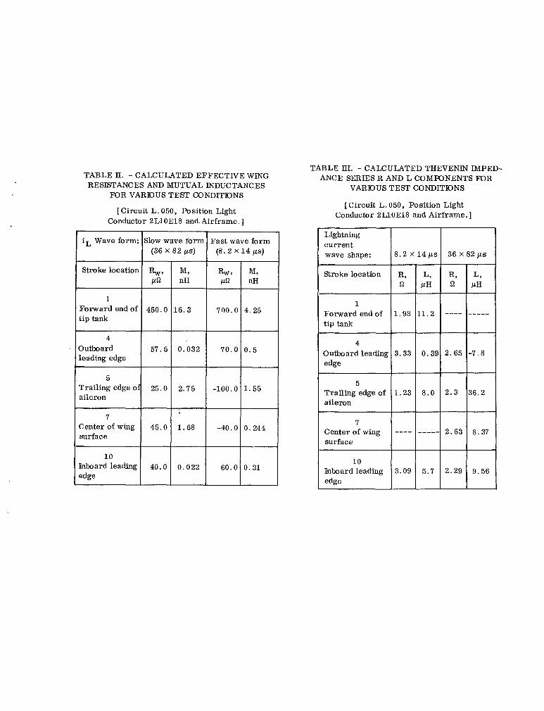
TABLE II. - CALCULATED EFFECTIVE WING RESISTANCES AND MUTUAL INDUCTANCES
FOR VARIOUS TEST CONDITIONS
[Circuit L. 050, Position Light Conductor 2L10E18 and Airframe.]
8 . 2 x 1 4 p s
L, PH
11.2
0.39
8.0
_----
5.7
36 x 8 2 p s
R, L, Q PH
---- -----
2.65 -7.8
2 .3 36.2
2.63 8.37
2.29 9.56
t ip tank
iL Wave form:
Outboard 1:idge 1 57*5
Trailing edge o 25. o
Slow wave form Fast wave form (36 X 82 ps) (8.2 X 1 4 ps)
Center: wing 1 45.0 surface
I n b a r d leading 40.0 edge
FJ-5 700. a
~
-100.0
-40.0 $
M, nH
4.25
0.5
1.55
0.244
0.31
TABLE III. - CALCULATED THEVENIN IMPED- ANCE SERIES R AND L COMPONENTS FOR
VARIOUS TEST CONDITIONS
I Circuit L. 050, Position Light Conductor 2L10E18 and Airframe. ]
Lightning current wave shape:
Stroke location
1 Forward end of tip tank
~
4 Outboard leading edge
5 Trailing edge of aileron
7 Center of wing surface
10 Inboard leading edge
R, Q
1.98
3.33
-
1.23

TABLE IV. - INDUCED VOLTAGES AND CURRENTS
[Circuit F.0511, E-11 Autopilot Conductors F572K18 and F755E18.1
Fast wave form (8.2 X 1 4 p s ) i, Wave form: Sow wave form (36 x 82 ps) Y
Stroke location
Open circuit
voltage e0c V
Short circuit :urrent
A is,
Voltage across l-ohm load, el 9
V
0.068
Zurreni ;hrough l-ohm load,
A il,
0.075
0 .1
Open circuit roltage:
eo, V
0 .4
3/0.48
1 Forward end of tip tank
0 . 3 0 .07
4 Outboard leading edge
0.2/ 0.12
27/0.1 0.25
5 Trailing edge of aileron
7 Center of wing surface
0.4/ 0.13
0.1 0.6 2/0.2
0.1
0.25
0.25 0.12 6/0.5
1.5/ 0.2
0.1
0.04 10
Inboard leading edge
0.1 0.25 0.04

TABLE V. - CALCULATED EFFECTIVE WING RESISTANCES AND MUTUAL INDUCTANCES
FOR VARIOUS TEST CONDITIONS
[Circuit F.0511, E-11 Autopilot Conductors F572K18 and F7 55318.1
Conductor
iL Wave form: Slow wave form (36 x 82 p s )
Open circuit voltage, V Short circuit current, A
Stroke location
Conductor-to - Conductor-to- airframe conductor
1 F o m a r d end of tip tank
4 Outboard leading edge
5 Trailing edge of aileron
Conductor -to - Conductor -to - airframe conductor
7 Center of wing surface '
Unshielded number 16 insulated conductor
RG 58A/U coaxial cable
10 Inboard leading edge
1 . 5 ---- 0.8 ---
1 . 2 1.6 --- __--
Rw 1
Parallel pair of number 1 6 insulated conductors
0.75
0.50
1.25
5.0 1 . 6 5.0 I 0.8
0.375
2.25
M, nH
-0.0185
-0.0684
-0.0392
-0.0169
-0.043
past wave form (8.2 x 14ps) I
nH
4.5 I -0.0698
2 . 0 I -0*187
8.25 -0.107
I 1.75 -0.0227 I
TABLE VI. - MAXIMUM INDUCED VOLTAGES AND CURRENTS IN NEW WING CIRCUITS
0.16 I 1 .0 1 0 .1 1 1.5 I Twisted pair of number 16 insulated conductors

TABLE VI[. - MAXIMUM INDUCED VOLTAGES AND CURRENTS IN NEW WING CIRCUITS
Conductor-to - conductor
[Series 2 - All circuits and shields connected to airframe at location between aileron and flap on trailing edge. Identical measurements on circuits terminating at leading and trailing edges. ]
Conductor-to - airframe
Conductor I open circuit voltage, v I a r t circuit current, A
Unshielded number 1 6 insulated conductor
RG 58A/U coaxial cable
Conductor-to - conductor
Leading Trailing edgea edgeb
2.0 0.4
2.1 0.4
Conductor-to- airframe
Unshielded number 1 6 insulated conductor
2.0 0.4
Leading Trailing edge 1 edge
RG 58A/U coaxial cable
Leading Trailing edge 1 edge
I 2.1 I 0.4
Leading edge
Trailing edge
Trailing edge
I ---
Leading edge
1 . 6
I ---
Leading edge
1 . 6
Leading edgea
Leading edge
Trailin edgeb
Trailing edge
1 . 3
Trailing edge
1 . 3
2.2 2.2 0 . 4 0 . 4 I ---- ---- ---
0.1
---
0.1 Twisted pair of number 16 1 1 . 0 I 0.5 insulated conductors Twisted pair of number 16 1 1 . 0 I 0.5 insulated conductors
0.9 0.9 1 . 4 1 . 4
Parallel pair of number 1 6 1 6.0 1 1.0 insulated conductors Parallel pair of number 1 6 1 6.0 1 1.0 insulated conductors
6.0 6.0 2.0 2.0 1 . 3 0.1
I
!et long. set long.
~
aCircuits terminating at leading edge a re 38 k i r c u i t s terminating at trailing edge are 1 2 aCircuits terminating at leading edge a re 38 feet long. k i r c u i t s terminating at trailing edge are 1 2 feet long.

LI GHTNlN G CURRENT IN, iL -\
\ \
\ \
t LI GHTNl NG CUR RENT OUT, i L
Figure 1. - C i rcu i t representation of a i rc ra f t wing- electr ical c i r c u i t combinat ion.
d i dt
V M = M - iL - 4J
a
Figure 2. - Circui t representation of wing structure and electrical circuit .

f
Figure 3. - Thevenin equiva
---m
WING POD-, \
P - 264"
l-'J LEADING EDGE
1
I /- L
/ /
Figure 4. - Schematic plan view o

,r WING TIP FUELTANK /'
/r SIMULATED LIGHTNING STROKE ,c MEASUREMENT
LIGHTNING CURRENT GENERATOR
I
FOIL GROUND ," CURRENT MEASURING SHUNT-/ RETURN PATH'
Figure 5. - F89J wing test setup.
Figure 6 . - F89J right wing shown positioned for test in high voltage laboratory test bay. Lightning c u r r e n t generator i s beneath tip tank.

3-"5991
Ti -
FRO
NT T
IME
T2 -
TIM
E TO
HAL
F VA
LUE
ON T
HE T
AIL
THE
WAV
E SH
APE
IS D
ESCR
IBED
BY
THE
NOTA
TION
: (T
i x T
2)
(A) l
tSLO
W W
AVE
SHAP
E" 3
6 x8
2 @.
-50
PERC
ENT
LEVE
L
Figu
re 7.
- S
imul
ate
light
ning
wav
e sh
ape
not a
t i on
18) V
AST
WAV
E SH
APE"
8.2x
14~
s.
Figu
re 8.
- Si
mul
ated
light
ning
curr
ent w
ave s
hape
s (110
kil
oam
pere
stro
kes.
appli
ed fo
r in
duce
d effe
cts m
easu
re-
men
tsl.

E25991
(A) O
PEN
CIRC
UIT
INDU
CED
VOLT
AGE.
Figu
re 9.
- S
imul
ated
ligh
tnin
g st
roke
loca
tions
. La
rge
circ
led
num
bers
indi
cate
loca
tions
sele
cted
for e
xten
sive
test
ing.
(8
1 SHO
RT C
IRCU
IT C
URRE
NT.
Figu
re 1
0. - O
pen
circ
uit i
nduc
ed v
olta
ge a
nd s
hort
cir
cuit
curr
ent.
40 k
il-
ampe
re 3
6 x 82
ps li
ghtn
ing
stro
ke to
loca
tion
l.

'L I I
LI GHTNING CURRENT
I / I I
eoc
I I I I I I
I I I I
I I
I I I I I 1 INDUCED VOLTAGE ! I
I I I I
I I I
Figure 11. - Typical l ightning current and induced voltage wave forms.

E-5991
"
WIR
ING
LOCA
TION
RIGH
T TI
P PO
D TK
+2
LlOE
18
----@-+@
-#Ii
i W
ING
POSI
TION
I
LIGH
T
Figu
re 1
2. - C
ircui
t 1.
050
posi
tion
light
s w
iring
sch
e-
mat
ic a
nd lo
catio
n F8
9J r
ight
win
g an
d tip
fuel
tank
.
NOTE
: OP
EN-C
IRCU
IT 1
NDU.
CED
VOLT
AGES
AND
SH
ORT-
CIRC
UIT
INDU
CED
CURR
ENTS
MEA
S-
URED
AT
TERM
INAL
S OF P
OSIT
ION
LIGH
T CI
RCUI
T.
(CIR
CUIT
1.0
50,
COND
UCTO
R 2r 2L
10E1
8 AN
D FR
AME)
50
r
I-' i5 er er 3
0
SIMU
LATE
D LI
GHTN
ING
CURR
ENT,
kA
Figu
re 1
3. - A
mplit
ude o
f ind
uced
effe
cts ve
rsus
ampl
itude
of
simul
ated
12 x
24
ps li
ghtn
ing
curr
ent d
ischa
rged
to lo
ca-
tion
num
ber 1
(forw
ard en
d of
wing
tip
fuel
tank)
.

(A) STROKE LOCATION NO. 1, FORWARD END OF WING TIP FUEL TANK,
(B) STROKE LOCATION NO. 4, OUTBOARD END OF LEADING EDGE.
(C) STROKE LOCATION NO. 5, OUTBOARD END OF AILERON.
(D) STROKE LOCATION NO. 7. BOrCOM CENTER OF WING,
OPEN CIRCUIT VOLTAGE SHORT CIRCUIT CURRENT
(E) STROKE LOCATION NO. 10, INBOARD LEADING EDGE OF WING.
Figure 14. - Open c i r c u i t voltages and shor t c i r c u i t cu r ren ts measured on terminals of c i r - c u i t L.050 (position light), conductor 2L10E18 to airframe. (36 x 82pec, 40 kiloampere simulated l i gh tn ing current . )

(A) STROKE LOCATION NO. 1, FORWARD END OF WING TIP FUEL TANK.
(B) STROKE LOCATION NO. 4, OUTBOARD END OF LEADING EDGE.
(C) STROKE LOCATION NO. 5, OUTBOARD END OF AILERON.
(D) STROKE LOCATION NO. 7, BOllOM CENTER OF-WING.
OPEN CIRCUIT VOLTAGE SHORT CIRCUIT CURRENT
(E) STROKE LOCATION NO. 10, INBOARD LEADING EDGE OF WING.
Figure 15. - Open c i r c u i t voltages and shor t c i r c u i t c u r r e n t measured o n te rmina ls of c i r - c u i t L.050 (position light), conductor 2L10E18 to airframe. ( 8 . 2 ~ 14 p e c , simulated l igh tn ing current.)

0 eT (CALCULATED) e, (MEASURED)
Figure 16. - Comparison of measured e, and calculated induced voltage wave shapes, resu l t ing f rom 40 kiloampere 8.2 x 14 p stroke to location 1.

SWITCH L W I RI NG LOCATl ON
RIGHT OUTERWING TB
7
RIGHT ROCKET SAFETY SWITCH
7. - Ci rcu i t F.0511 E-11 autopilot flap position monitor ing switch w i r i ng schematic and location F89J r igh t wing and t i p fuel tank.

BEGINNING OF COPPER BRAID SHIELDING (BRAID IS SOLIDLY GROUNDED AT THIS POINT AND AT VARIOUS POINTS
EDGE. )--* ALONG TRA1UI’JG-c
:LIGHTNING CURRENT STROKE TO THE TANK \
Figure 18. - F-89 Wing showing additional circuits placed in the wing for test.
NASA-Lewis-Com’l