alow-voltage mos cascode current mirror for all current...
TRANSCRIPT

A Low-Voltage MOS Cascode Current Mirrorfor All Current Levels
Bradley A. Minch
Mixed Analog-Digital VLSI Circuits and Systems LabCornell University
Ithaca, NY 14853–5401
August 6, 2002
ORNELLC
1
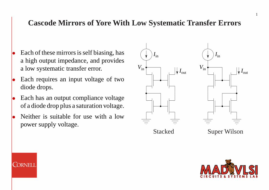
Cascode Mirrors of Yore With Low Systematic Transfer Errors
• Each of these mirrors is self biasing, hasa high output impedance, and providesa low systematic transfer error.
• Each requires an input voltage of twodiode drops.
• Each has an output compliance voltageof a diode drop plus a saturation voltage.
• Neither is suitable for use with a lowpower supply voltage.
Iin
IoutVin
Iin
IoutVin
Stacked Super Wilson
ORNELLC
2
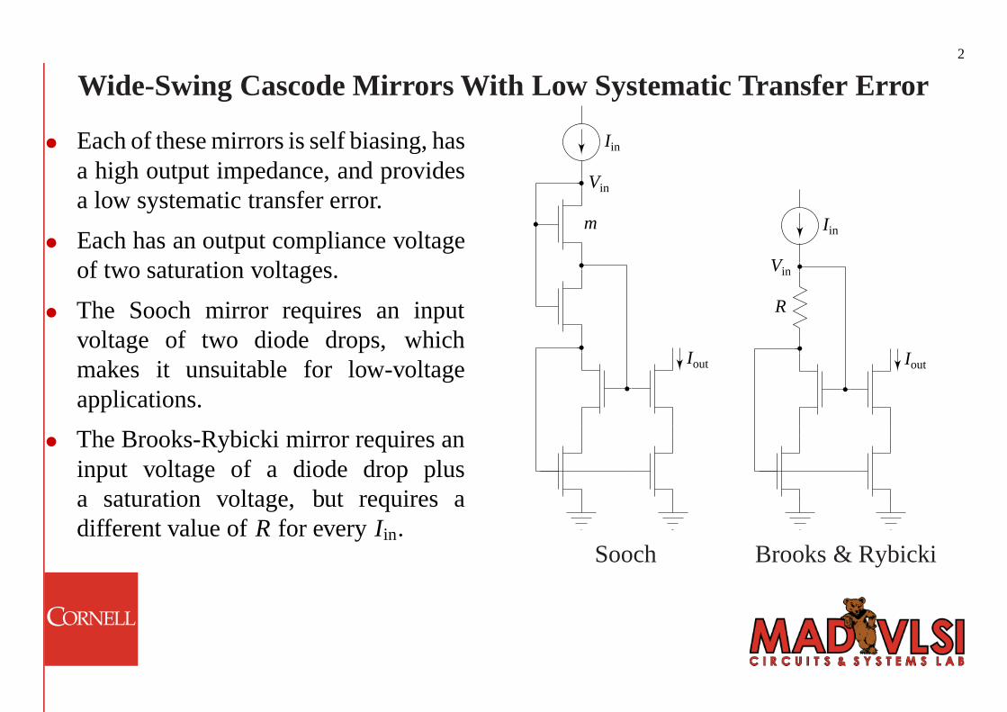
Wide-Swing Cascode Mirrors With Low Systematic Transfer Error
• Each of these mirrors is self biasing, hasa high output impedance, and providesa low systematic transfer error.
• Each has an output compliance voltageof two saturation voltages.
• The Sooch mirror requires an inputvoltage of two diode drops, whichmakes it unsuitable for low-voltageapplications.
• The Brooks-Rybicki mirror requires aninput voltage of a diode drop plusa saturation voltage, but requires adifferent value of R for every Iin.
Iout
Iin
Vin
m
Iout
Iin
Vin
R
Sooch Brooks & Rybicki
ORNELLC
2
Wide-Swing Cascode Mirrors With Low Systematic Transfer Error
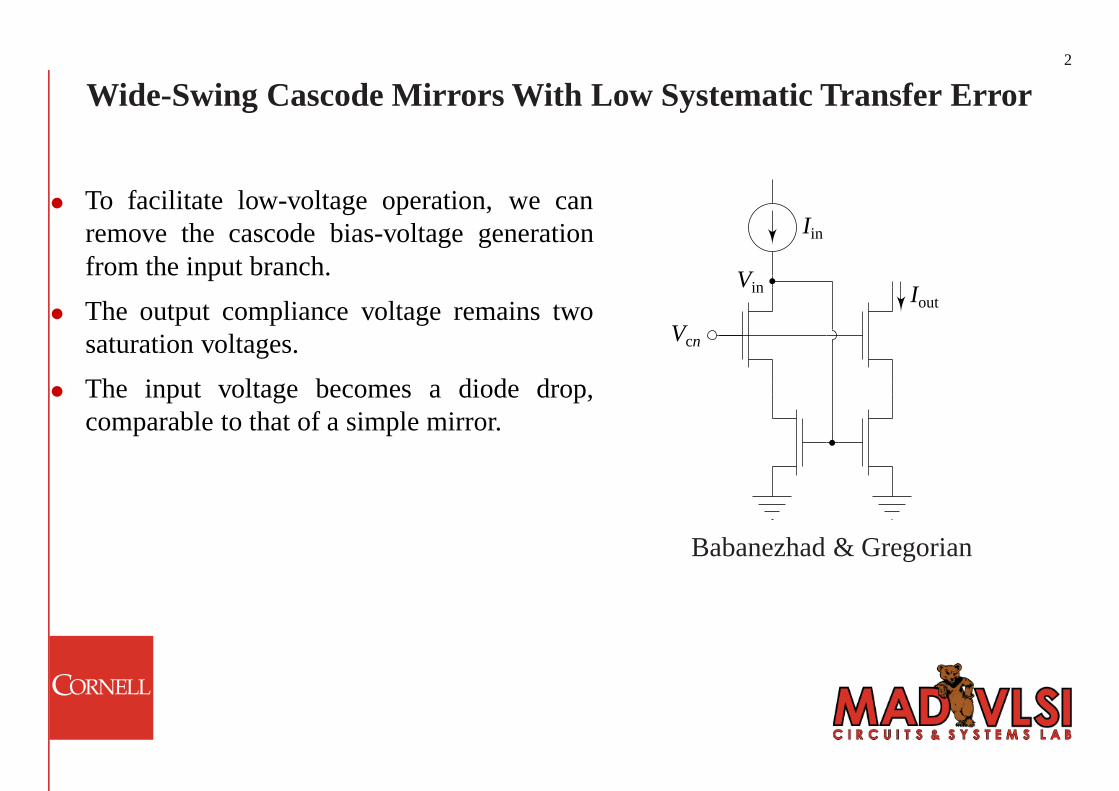
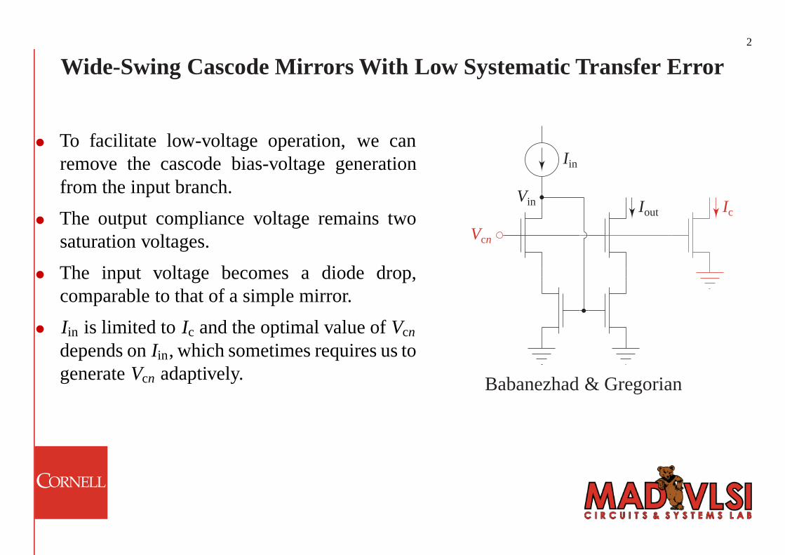
• To facilitate low-voltage operation, we canremove the cascode bias-voltage generationfrom the input branch.
• The output compliance voltage remains twosaturation voltages.
• The input voltage becomes a diode drop,comparable to that of a simple mirror.
• Iin is limited to Ic and the optimal value of Vcn
depends on Iin, which sometimes requires us togenerate Vcn adaptively.
Iout
Iin
Vin
Vcn
Ic
Babanezhad & Gregorian
ORNELLC
2
Wide-Swing Cascode Mirrors With Low Systematic Transfer Error
• To facilitate low-voltage operation, we canremove the cascode bias-voltage generationfrom the input branch.
• The output compliance voltage remains twosaturation voltages.
• The input voltage becomes a diode drop,comparable to that of a simple mirror.
• Iin is limited to Ic and the optimal value of Vcn
depends on Iin, which sometimes requires us togenerate Vcn adaptively.
Iout
Iin
Vin
Vcn
Ic
Babanezhad & Gregorian
ORNELLC

2
Wide-Swing Cascode Mirrors With Low Systematic Transfer Error
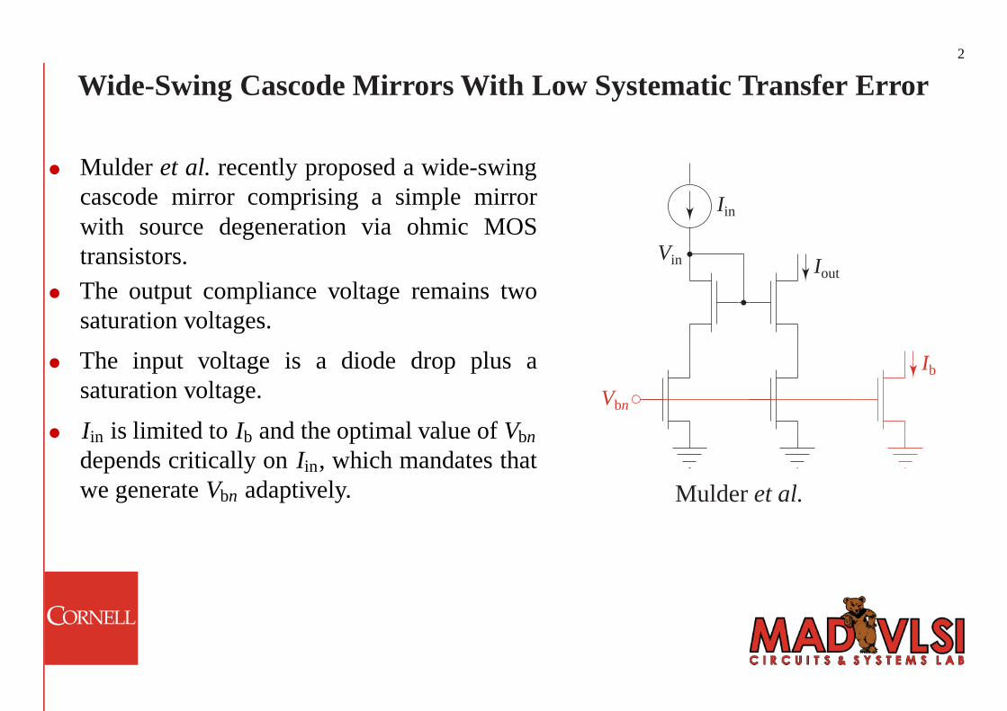
• Mulder et al. recently proposed a wide-swingcascode mirror comprising a simple mirrorwith source degeneration via ohmic MOStransistors.
• The output compliance voltage remains twosaturation voltages.
• The input voltage is a diode drop plus asaturation voltage.
• Iin is limited to Ib and the optimal value of Vbn
depends critically on Iin, which mandates thatwe generate Vbn adaptively.
Iout
Iin
Vin
Vbn
Ib
Mulder et al.
ORNELLC
2
Wide-Swing Cascode Mirrors With Low Systematic Transfer Error
• Mulder et al. recently proposed a wide-swingcascode mirror comprising a simple mirrorwith source degeneration via ohmic MOStransistors.
• The output compliance voltage remains twosaturation voltages.
• The input voltage is a diode drop plus asaturation voltage.
• Iin is limited to Ib and the optimal value of Vbn
depends critically on Iin, which mandates thatwe generate Vbn adaptively.
Iout
Iin
Vin
Vbn
Ib
Mulder et al.
ORNELLC
3
Development of a New Low-Voltage Cascode Current Mirror
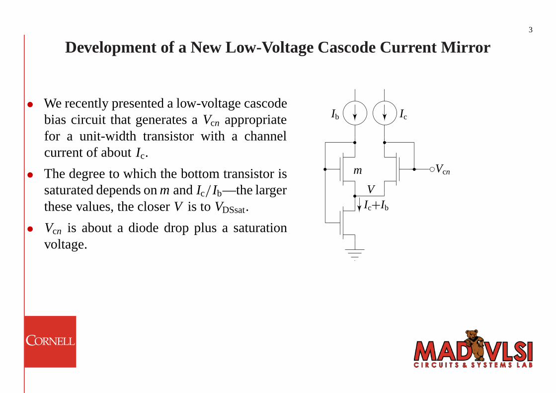
• We recently presented a low-voltage cascodebias circuit that generates a Vcn appropriatefor a unit-width transistor with a channelcurrent of about Ic.
• The degree to which the bottom transistor issaturated depends on m and Ic/Ib—the largerthese values, the closer V is to VDSsat.
• Vcn is about a diode drop plus a saturationvoltage.
m
Ib Ic
Ic+Ib
V
Vcn
ORNELLC

3
Development of a New Low-Voltage Cascode Current Mirror
• Suppose we take this circuit and make Ic theinput current.
• Then, we produce an output current by addingtwo transistors, as shown.
• In this mirror, V ′ will be slightly lower thanV , giving rise to a systematic transfer errror.In fact, it is easy to see that Iin < Iout <
Iin + Ib. If Iin � Ib, this systematic error isnegligible.
m
Ib Iin
Iin+Ib
V
Vin
ORNELLC

3
Development of a New Low-Voltage Cascode Current Mirror
• Suppose we take this circuit and make Ic theinput current.
• Then, we produce an output current by addingtwo transistors, as shown.
• In this mirror, V ′ will be slightly lower thanV , giving rise to a systematic transfer errror.In fact, it is easy to see that Iin < Iout <
Iin + Ib. If Iin � Ib, this systematic error isnegligible.
m
Ib Iin
Iin+Ib
V
IoutVin
Iout+V¢
ORNELLC
3
Development of a New Low-Voltage Cascode Current Mirror
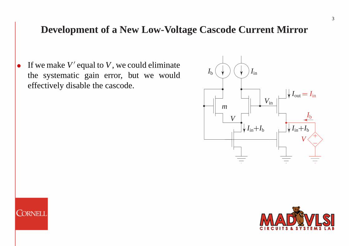
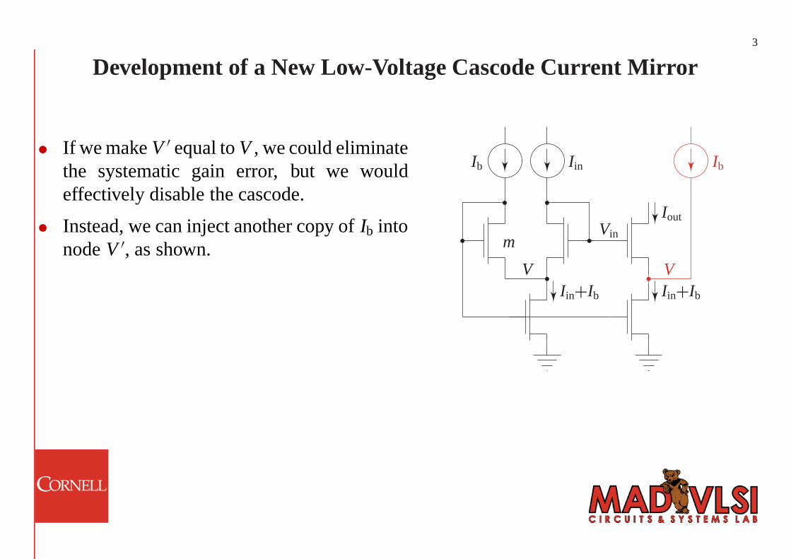
• If we make V ′ equal to V , we could eliminatethe systematic gain error, but we wouldeffectively disable the cascode.
• Instead, we can inject another copy of Ib intonode V ′, as shown.
• If Ib is generated by a saturated pMOStransistor, we can improve the circuit furtherby adding a diode-connected transistor ofwidth m, as shown.
m
Ib Iin
Iin+Ib
V
Iout = IinVin
Iin+Ib
V
Ib
ORNELLC
3
Development of a New Low-Voltage Cascode Current Mirror
• If we make V ′ equal to V , we could eliminatethe systematic gain error, but we wouldeffectively disable the cascode.
• Instead, we can inject another copy of Ib intonode V ′, as shown.
• If Ib is generated by a saturated pMOStransistor, we can improve the circuit furtherby adding a diode-connected transistor ofwidth m, as shown.
Ib
m
Ib Iin
Iin+Ib
V
IoutVin
Iin+Ib
V
ORNELLC

3
Development of a New Low-Voltage Cascode Current Mirror
• If we make V ′ equal to V , we could eliminatethe systematic gain error, but we wouldeffectively disable the cascode.
• Instead, we can inject another copy of Ib intonode V ′, as shown.
• If Ib is generated by a saturated pMOStransistor, we can improve the circuit furtherby adding a diode-connected transistor ofwidth m, as shown.
Ib
m
Ib Iin
Iin+Ib
V
IoutVin
m
Iin+Ib
V
ORNELLC
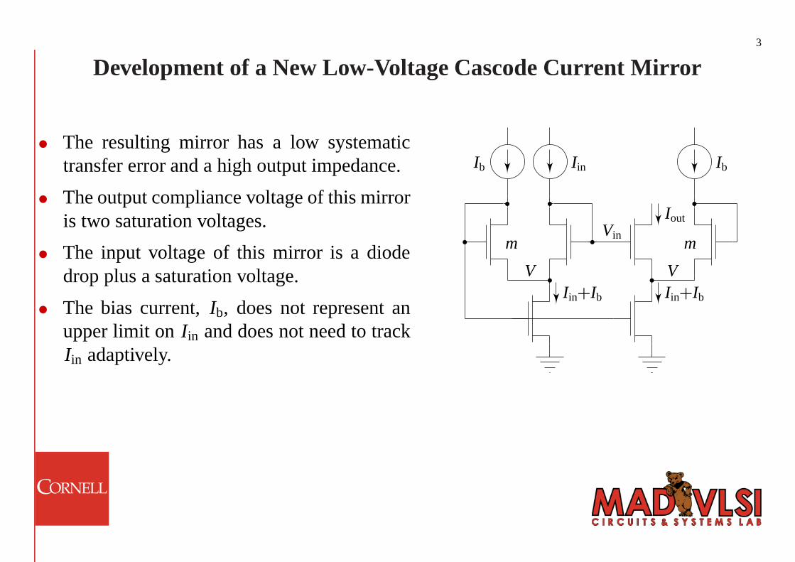
3
Development of a New Low-Voltage Cascode Current Mirror
• The resulting mirror has a low systematictransfer error and a high output impedance.
• The output compliance voltage of this mirroris two saturation voltages.
• The input voltage of this mirror is a diodedrop plus a saturation voltage.
• The bias current, Ib, does not represent anupper limit on Iin and does not need to trackIin adaptively.
Ib
m
Ib Iin
Iin+Ib
V
IoutVin
m
Iin+Ib
V
ORNELLC
4
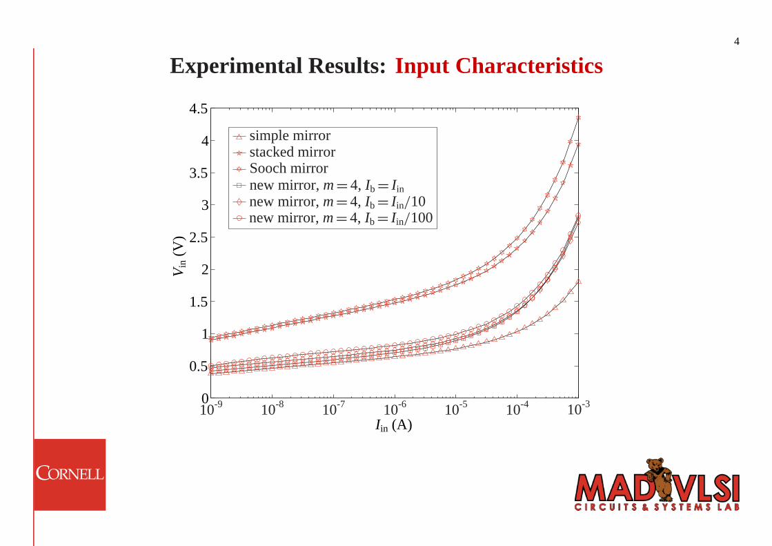
Experimental Results: Input Characteristics
simple mirrorstacked mirrorSooch mirrornew mirror, m = 4, Ib = Iin
new mirror, m = 4, Ib = Iin/10new mirror, m = 4, Ib = Iin/100
0
0.5
1
1.5
2
2.5
3
3.5
4
4.5
Iin (A)
Vin
(V
)
10-9 10-8 10-7 10-6 10-5 10-4 10-3
ORNELLC

4
Experimental Results: Output Characteristics Iin = 1.00 nA
0 0.5 1 1.5 2 2.5 3 3.5 4 4.5 51.02
1.03
1.04
1.05
1.06
1.07
1.08
1.09
1.1
1.11
1.12
Vout (V)
I out
(nA
)
simple mirrorstacked mirrorSooch mirrornew mirror, m = 4, Ib = Iin
new mirror, m = 4, Ib = Iin/10new mirror, m = 4, Ib = Iin/100
ORNELLC

4
Experimental Results: Output Characteristics Iin = 10.0 nA
0 0.5 1 1.5 2 2.5 3 3.5 4 4.5 510.1
10.2
10.3
10.4
10.5
10.6
10.7
10.8
10.9
11
11.1
Vout (V)
I out
(nA
)
simple mirrorstacked mirrorSooch mirrornew mirror, m = 4, Ib = Iin
new mirror, m = 4, Ib = Iin/10new mirror, m = 4, Ib = Iin/100
ORNELLC

4
Experimental Results: Output Characteristics Iin = 100.nA
0 0.5 1 1.5 2 2.5 3 3.5 4 4.5 5101
102
103
104
105
106
107
108
109
110
111
Vout (V)
I out
(nA
)
simple mirrorstacked mirrorSooch mirrornew mirror, m = 4, Ib = Iin
new mirror, m = 4, Ib = Iin/10new mirror, m = 4, Ib = Iin/100
ORNELLC

4
Experimental Results: Output Characteristics Iin = 1.00µA
0 0.5 1 1.5 2 2.5 3 3.5 4 4.5 51
1.01
1.02
1.03
1.04
1.05
1.06
1.07
1.08
1.09
1.1
Vout (V)
I out
(m
A)
simple mirrorstacked mirrorSooch mirrornew mirror, m = 4, Ib = Iin
new mirror, m = 4, Ib = Iin/10new mirror, m = 4, Ib = Iin/100
ORNELLC

4
Experimental Results: Output Characteristics Iin = 10.0µA
0 0.5 1 1.5 2 2.5 3 3.5 4 4.5 59.7
9.8
9.9
10
10.1
10.2
10.3
10.4
10.5
10.6
10.7
Vout (V)
I out
(m
A)
simple mirrorstacked mirrorSooch mirrornew mirror, m = 4, Ib = Iin
new mirror, m = 4, Ib = Iin/10new mirror, m = 4, Ib = Iin/100
ORNELLC

4
Experimental Results: Output Characteristics Iin = 100.µA
0 0.5 1 1.5 2 2.5 3 3.5 4 4.5 595
96
97
98
99
100
101
102
103
104
105
Vout (V)
I out
(m
A)
simple mirrorstacked mirrorSooch mirrornew mirror, m = 4, Ib = Iin
new mirror, m = 4, Ib = Iin/10new mirror, m = 4, Ib = Iin/100
ORNELLC

4
Experimental Results: Output Characteristics Iin = 1.00 mA
0 0.5 1 1.5 2 2.5 3 3.5 4 4.5 50.91
0.92
0.93
0.94
0.95
0.96
0.97
0.98
0.99
1
1.01
Vout (V)
I out
(m
A)
simple mirrorstacked mirrorSooch mirrornew mirror, m = 4, Ib = Iin
new mirror, m = 4, Ib = Iin/10new mirror, m = 4, Ib = Iin/100
ORNELLC