a current mirror based two stage cmos cascode …jestec.taylors.edu.my/vol 12 issue 3 march...
TRANSCRIPT
Journal of Engineering Science and Technology Vol. 12, No. 3 (2017) 686 - 700 © School of Engineering, Taylor’s University
686
A CURRENT MIRROR BASED TWO STAGE CMOS CASCODE OP-AMP FOR HIGH FREQUENCY APPLICATION
RAMKRISHNA KUNDU, ABHISHEK PANDEY*, SUBHRA CHAKRABORTY, VIJAY NATH
VLSI Design Group, Department of Electronics and Communication Engineering,
Birla Institute of Technology, Mesra, 835215, Ranchi, Jharkhand, India
*Corresponding Author: [email protected]
Abstract
This paper presents a low power, high slew rate, high gain, ultra wide band two
stage CMOS cascode operational amplifier for radio frequency application.
Current mirror based cascoding technique and pole zero cancelation technique is
used to ameliorate the gain and enhance the unity gain bandwidth respectively,
which is the novelty of the circuit. In cascading technique a common source
transistor drive a common gate transistor. The cascoding is used to enhance the
output resistance and hence improve the overall gain of the operational amplifier
with less complexity and less power dissipation. To bias the common gate
transistor, a current mirror is used in this paper. The proposed circuit is designed
and simulated using Cadence analog and digital system design tools of 45
nanometer CMOS technology. The simulated results of the circuit show DC gain
of 63.62 dB, unity gain bandwidth of 2.70 GHz, slew rate of 1816 V/µs, phase
margin of 59.53º, power supply of the proposed operational amplifier is 1.4 V
(rail-to-rail ±700 mV), and power consumption is 0.71 mW. This circuit
specification has encountered the requirements of radio frequency application.
Keywords: Current mirror, Gain, Bandwidth, Slew rate, Power consumption, Cascode.
1. Introduction
In modern days due to the sophisticated silicon processing technology, the
channel length of the metal oxide semiconductor field effect transistor (MOSFET)
penetrates the nanometer regime. With the reduction in channel length, the transit
frequency of the MOSFET increases. This opens the doors of radio frequency
application for the very large scale integration (VLSI) technology. Today a total

A Current Mirror Based Two Stage CMOS Cascode Op-Amp for High . . . . 687
Journal of Engineering Science and Technology March 2017, Vol. 12(3)
Nomenclatures
AV Overall Gain (suffix I and II denote first and second stage gain
respectively)
CC Shunt capacitance, F
Cgd Gate to Drain capacitance, F
Cgs Gate to source capacitance, F
CI Total capacitance at the interface between first and second stage, F
CII Total capacitance between the output node and ground, F
CL Load Capacitance, F
Cox Gate Oxide capacitance, F
D Total harmonic distortion in dB
fT The transit frequency of the MOSFET, Hz
gm Transconductance of transistor (subscript C2, C4, 1, 2, 3, 4, 6, 7,
8 and 12 denote the transconductance of transistor MC2, MC4,
M1, M2, M3, M4, M6, M7, M8 and M12 respectively), mA/V
gmI Transconductance of input stage of transistor M1, mA/V
gmII Transconductance of input stage of transistor M6, mA/V
I Current (subscript MB1 and MB2 denotes current in transistor
MB1 and MB2 respectively), A
K Total harmonic distortion in %
L Channel or Technology length, m
Lov Overlap Length (0.05 to 0.1 L), m
rds Drain to source resistance (subscript C2, C4, 2, 4, 6, 7, 11 and 12
denote the drain to source resistance of transistor MC2, MC4,
M2, M4, M6, M7, M11 and M12 respectively), Ω
RI Output resistance of the first stage, Ω
RII Output resistance of the second stage, Ω
ro The output resistance of the transistor (subscript 2, 4, 6, 7, 8 and
9 denote the output resistance of the transistor M2, M4, M6, M7,
M8, and M9 respectively), Ω
RZ Nulling resistor, Ω
Vds Drain to source voltage, V
W Channel width, m
W/L Aspect ratio
Abbreviations
CMRR Common Mode Rejection Ratio
GB Gain Bandwidth, Hz
RHP Right Half Plane
THD Total Harmonic Distortion
UGB Unity Gain Bandwidth, Hz
transceiver can be implemented in a system on chip (SOC). This radio frequency
integrated circuit (RFIC) technology is in high demand for the VLSI
implementation of computer processors, as the clock frequency of computer’s
processors has reached the GHz range. Operational amplifier (op-amp) is one of
the versatile components in analog integrated circuits. It almost plays the same
role as a logic gate in digital electronics.
688 R. Kundu et al.
Journal of Engineering Science and Technology March 2017, Vol. 12(3)
Op-amp can be used in summer, substractor, multiplier, integrator,
differentiator, active filter, digital to analog converter, and analog to digital
converter. High frequency application requires a high speed op-amp. To make a
high speed op-amp, its unity gain bandwidth (UGB) should be very high. It is a
challenge for the analog circuit designer to design an op-amp, which has high
unity gain bandwidth with moderate DC gain. Since most of the portable devices
are battery operated. Therefore, the power consumption of the designed circuit
should be low. The high gain amplifier uses cascode structure or multistage
design with long channel length transistor biased at low current levels, whereas
high bandwidth amplifiers uses single stage design with short channel length
transistor biased at high current levels.
On the basis of literature review several op-amps have been found that
designed in different techniques. In a fully differential op-amp, both input and
output are in differential mode. In this type of op-amp, besides the differential-
mode signal, the common mode signal should also be considered. If the common
mode signal is not low, the differential mode signal will be limited. At the output
of the op-amp, common mode is influenced by the mismatches and a load affects
the output swing. This requires extra common mode stabilization circuitry and
this increases the complexity and power consumption. A high gain fully
differential amplifier shows an adequate gain at low power supply. However, the
unity gain bandwidth is not good for wireless application [1 - 3]. To improve the
UGB, doublet free pole-Zero cancelation and gm- boosting techniques is used but
the power consumption is very high. Therefore, this is not suitable for battery
operated devices. Due to mismatch in input and output differential mode the
circuit complexity increases and thus increases power consumption. The slew rate
and UGB is also the limitation of fully differential amplifier.
In bulk driven MOSFET the transistor is switched ON by applying a signal to
the body terminal instead of applying signal on the gate terminal. There are
several papers on op-amp based on the bulk driven transistor [4 - 6], which shows
also a less UGB. Therefore, it is not applicable for wireless application. On the
other hand the main disadvantage for the op-amp design with bulk driven
complementary metal oxide semiconductor (CMOS) is that it is exposed to the
problem of latch up effect. Therefore, the input transconductance of the bulk
driven CMOS is 4 to 5 times smaller than the input transconductance of gate
driven CMOS. Consequently, the gain will be reduced. To improve the gain, a
partial positive feedback circuit can be used, but it will increase the complexity
and also the power consumption.
In several literatures the gain of the op-amp is increased by using several
stages. A three stage CMOS op-amp with nested miller capacitance has been
designed [7]. In multistage op-amp the UGB is limited by the parasitic poles for
analog CMOS. This is better than two as mentioned above fully differential and
bulk drive method.
In most of the design the gain is high, but UGB is not so good. But for
radio frequency application and high speed application, it should be better
matching between gain, UGB, phase margin and power consumption. In this
paper a novel approach on current mirror based cascoding technique has been
proposed, which shows high UGB, moderate DC gain, high slew rate and low
power dissipation.

A Current Mirror Based Two Stage CMOS Cascode Op-Amp for High . . . . 689
Journal of Engineering Science and Technology March 2017, Vol. 12(3)
2. Methodology
The design of an operational amplifier with high UGB and moderate DC gain is
challenging task for an analog designer. Due to the advancement of silicon
processing technology, the channel length of the MOSFET decreases
dramatically. This provides the analog designer more potential to achieve high
unity gain bandwidth [8]. But continuously decreasing of the channel length of
MOSFET creates other challenges.
Nowadays the designer is more concern about the power consumption of the
circuit, because most of the portable electronic devices are battery operated.
Therefore, the power consumption of the circuit should be less to improve the
battery lifetime. For that reason the supply voltage is also reduced.
In many literatures, it is mentioned that the design of operational amplifier
with moderate DC gain and high unity gain bandwidth at low supply voltages
requires three or even more stages. But this proposed circuit uses a two stage
operational amplifier for achieving moderate DC gain and high unity gain
bandwidth. A simple two stage op-amp consists of differential stage and an
inverting stage. But the high unity gain bandwidth with moderate DC gain
cannot be achieved using this. With the reduction of power supply the input
common mode range (ICMR) and power supply rejection ratio (PSRR)
performance of the circuit also reduces. Actually the gain of the op-amp is the
product of product of transconductances of two stages and product of output
resistances of two stages. To improve the gain there are three methods- (1).
Increase the number of the stage, (2). Increase the transconductance and (3).
Increase the output resistance.
Now (1) if the number of stages is increased, the stability of the circuit will
be diminished and (2) since the transconductance is directly proportional to the
drain current, so if transconductance is improving the drain current also increases
and it increases the power dissipation.
Since the output resistance (3) is inversely proportional to the drain current,
so by increasing the output resistance the gain will be improved and power
consumption will be reduced.
2.1. Cascoding with the first stage
To implement the cascoding technique, a common source transistor and a
common gate transistor is used, where common source transistor drives the
common gate transistor. This cascoding technique can be used in the first stage or
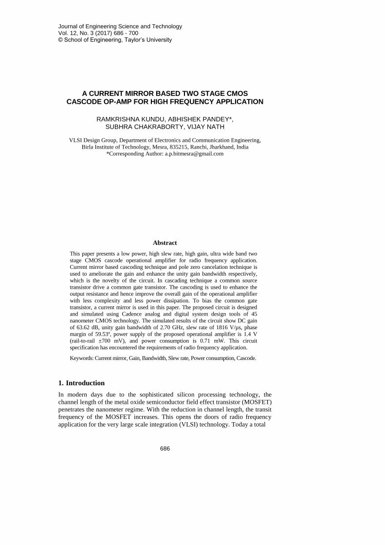
in the second stage. The circuit shown in Fig. 1 [8] illustrates how cascoding can
be used in the first stage.
In this circuit (Fig. 1) transistor M3, M4, MC3, MC4 and M9 is used to
implement the current mirror load. Transistor MC3 and MC4 increases the gain of
the first stage by increasing the output resistance which is given by
444222 dsdsCmCdsdsCmCI rrgrrgR (1)
Transistor M1, M2, MC1 and MC2 implement the cascoding technique at the
input. Transistor MB1 through MB5 is used to provide the DC bias to the
690 R. Kundu et al.
Journal of Engineering Science and Technology March 2017, Vol. 12(3)
transistor MC1 and MC2. The drain voltage of MB1 and MB2 applied to the
input of p-channel current mirror. The bias current of MOS diode MB5 is
provided by MB3 and MB4.
Fig. 1. CMOS op-amp with Cascoding in first stage.
The W/L ratios between M1, M2 and MB1, MB2 determines the DC
currents IMB1+IMB2 through MB5, which creates the bias voltage for MC1 and
MC2. In the second stage a push pull inverter is used. In the push pull inverter
M6 is a common source p-channel transistor and M7 is a common source n-
channel transistor. The common source p-channel metal oxide semiconductor
(PMOS) output transistor drive directly from the differential input stage. This
increases Vds (saturation), which degrades the output common mode range
performance. That is why a voltage translation is performed before driving the
gate of the output PMOS transistor. The transistor MT1 and MT2 perform the
task of voltage translation. MT2 is a current source which biases the source
follower transistor MT1. The small signal gain of the output of the differential
stage to the output of the voltage translator is close to unity and provides a
small amount of phase shift.
2.2. Cascoding with second stage
To avoid the complexity of level shifter, the cascoding in second stage
architecture [8, 9] is proposed, which is shown in Fig. 2. In this op-amp it is noted
that gain and stability behaves as opposite nature. This architecture will provide
the trade-offs between gain and stability. It is very well known that unity gain
bandwidth is given as
A Current Mirror Based Two Stage CMOS Cascode Op-Amp for High . . . . 691
Journal of Engineering Science and Technology March 2017, Vol. 12(3)
L
mI
C
gGB (2)
where gmI input transconductance and CL is the capacitor which is connected from
output to ground terminal. A very high unity gain bandwidth can be obtained if
input transconductance is very high and value of CL is very small. The input
transconductance may be defined as the transconductance of transistor M1 or M2.
As it is known that transconductance is directly proportional to the square root of
channel width to channel length ratio. This is the reason to make the channel
width of M1 and M2 larger and CL is reduced. Slew rate is inversely proportional
to CL. Consequently, slew rate increases as CL is reduced.
Fig. 2. CMOS op-amp with Cascoding in second stage.
In this op-amp the gain of the first stage is reduced by using M3 and M4 as
active load. As the gain of the first stage is reduced the output pole on the first
stage is increased due to lower resistance of M4 to AC ground. The output signal
from the first stage is differentially applied to the cascoded output stage. The
maximum gain comes from the second stage.
The gain from the second stage is-
3
1
4
2
m
m
m
m
VIg
g
g
gA (3)
where gm is transconductance and suffix denotes transistor number. The gain of
the second stage is
IImm
VII Rgg
A )2
( 86 (4)
692 R. Kundu et al.
Journal of Engineering Science and Technology March 2017, Vol. 12(3)
111212677 | | dsdsmdsdsmII rrgrrgR (5)
So the overall gain
II
mm
m
m
VIIVV Rgg
g
gAAA )
2( 86
4
2
1
(6)
The presence of dominant pole is now at the output. Op-amp is self-
compensated by shunt capacitance CC at the output. In this circuit M16 and M17
is act as active load, which replaced by MOS transistor because resistors are very
tedious to fabricate. But this circuit is more complex and the DC gain is not good.
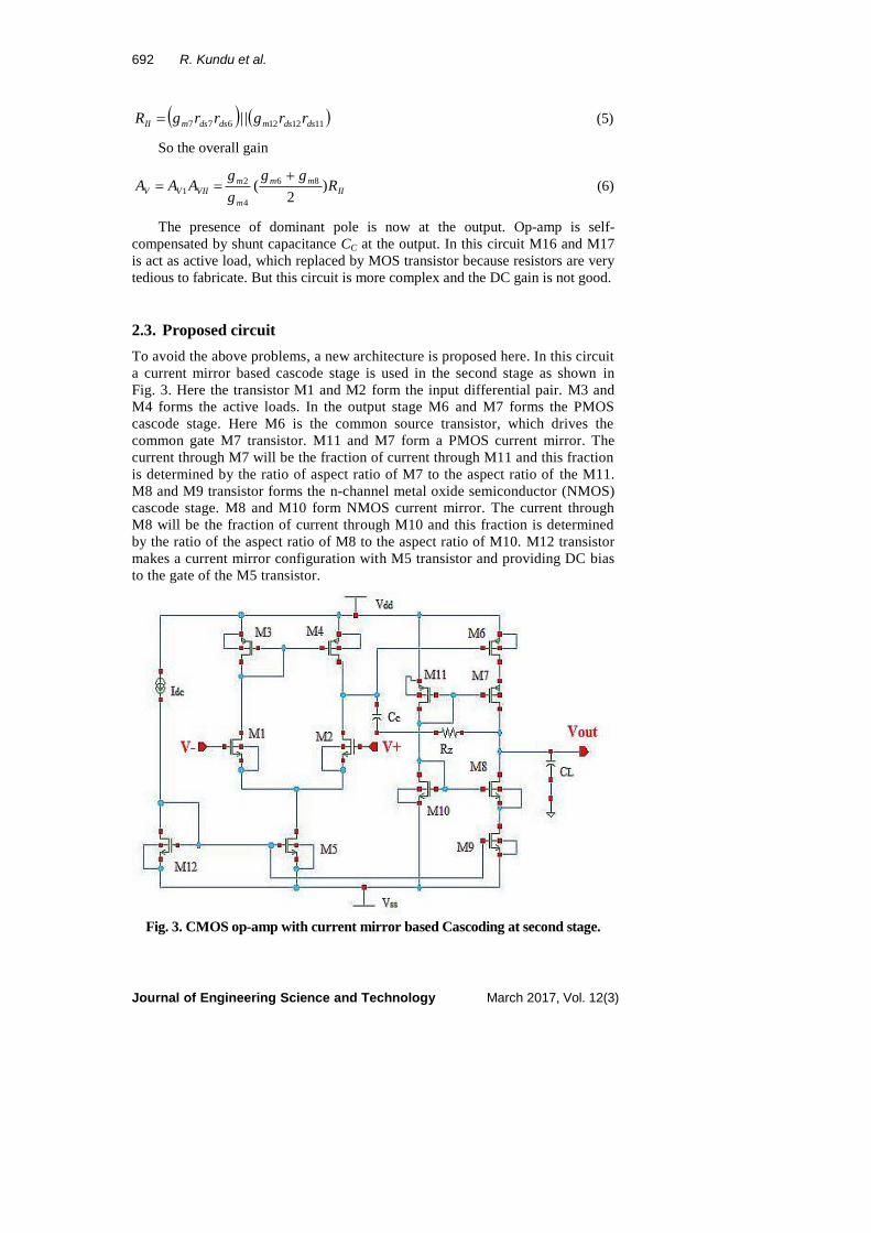
2.3. Proposed circuit
To avoid the above problems, a new architecture is proposed here. In this circuit
a current mirror based cascode stage is used in the second stage as shown in
Fig. 3. Here the transistor M1 and M2 form the input differential pair. M3 and
M4 forms the active loads. In the output stage M6 and M7 forms the PMOS
cascode stage. Here M6 is the common source transistor, which drives the
common gate M7 transistor. M11 and M7 form a PMOS current mirror. The
current through M7 will be the fraction of current through M11 and this fraction
is determined by the ratio of aspect ratio of M7 to the aspect ratio of the M11.
M8 and M9 transistor forms the n-channel metal oxide semiconductor (NMOS)
cascode stage. M8 and M10 form NMOS current mirror. The current through
M8 will be the fraction of current through M10 and this fraction is determined
by the ratio of the aspect ratio of M8 to the aspect ratio of M10. M12 transistor
makes a current mirror configuration with M5 transistor and providing DC bias
to the gate of the M5 transistor.
Fig. 3. CMOS op-amp with current mirror based Cascoding at second stage.
A Current Mirror Based Two Stage CMOS Cascode Op-Amp for High . . . . 693
Journal of Engineering Science and Technology March 2017, Vol. 12(3)
In Fig. 3, M9 is the common source transistor, which drives the common
gate M8 transistor. Here M11 transistor forms a current mirror with the
transistor M7 and provides DC biasing to the gate of the M7 transistor. M10
transistor forms a current mirror with the M8 transistor and provides DC biasing
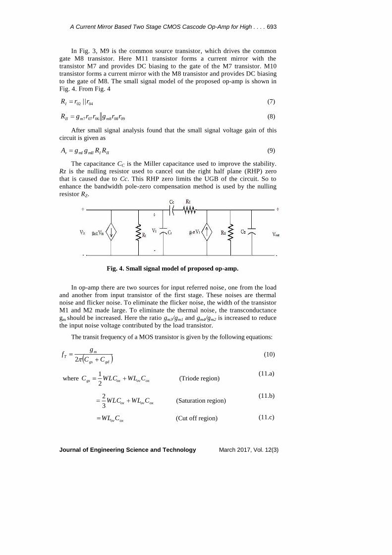
to the gate of M8. The small signal model of the proposed op-amp is shown in
Fig. 4. From Fig. 4
0402 | |rrRI (7)
0908806077 rrgrrgR mmII (8)
After small signal analysis found that the small signal voltage gain of this
circuit is given as
IIImIImIv RRggA (9)
The capacitance CC is the Miller capacitance used to improve the stability.
Rz is the nulling resistor used to cancel out the right half plane (RHP) zero
that is caused due to Cc. This RHP zero limits the UGB of the circuit. So to
enhance the bandwidth pole-zero compensation method is used by the nulling
resistor RZ.
Fig. 4. Small signal model of proposed op-amp.
In op-amp there are two sources for input referred noise, one from the load
and another from input transistor of the first stage. These noises are thermal
noise and flicker noise. To eliminate the flicker noise, the width of the transistor
M1 and M2 made large. To eliminate the thermal noise, the transconductance
gm should be increased. Here the ratio gm3/gm1 and gm4/gm2 is increased to reduce
the input noise voltage contributed by the load transistor.
The transit frequency of a MOS transistor is given by the following equations:
gdgs
m
TCC
gf
2 (10)
where oxovoxgs CWLWLCC 2
1 (Triode region)
(11.a)
oxovox CWLWLC 3
2 (Saturation region)
(11.b)
oxovCWL (Cut off region) (11.c)
694 R. Kundu et al.
Journal of Engineering Science and Technology March 2017, Vol. 12(3)
and oxovoxgd CWLWLCC 2
1 (Triode region)
(12.a)
oxovCWL (Saturation region) (12.b)
oxovCWL (Cut off region) (12.c)
From the above Eq. (10), we can conclude that the transit frequency is
inversely proportional to the channel length. In the proposed circuit channel
length of 45nm is used, which is very small. That is why it produces a very high
unity gain bandwidth. Eqs. (11) and (12) represent the value of Cgs and Cgd at
different region such as triode, saturation and cut off.
With the reduction of channel length, the threshold voltage is also reduced.
For this reason, transistor can operate at very low power supply which leads to
low power consumption by the transistor. In the proposed circuit the number of
transistor is less than the previous two. So the overall power consumption of the
circuit is very less.
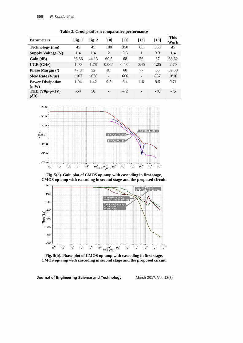
3. Results and Discussion
In this paper the op-amp circuits have been designed and simulated in a 45nm
CMOS process by Cadence analog and digital design tools. The simulation
result of proposed op-amp is compared with cascoding in first stage and
cascoding in a second stage op-amp. AC response of proposed op-amp,
cascoding in first stage and cascoding in the second stage are shown in Fig. 5
with same capacitor load of 0.5pF. The CMOS op-amp with produces a UGB of
1.00 GHz, DC gain of 36.86dB, phase margin of 47.8º, slew rate of 1107V/µs
and power dissipation of 1.04 mW. A UGB of 1.78 GHz, DC gain of 44.13 dB,
phase margin of 52º, slew rate of 1678V/µs and power dissipation of 1.42 mW
was observed in CMOS op-amp with cascading in second stage. The proposed
op-amp has given in Fig. 3, produces superior results than the above designed
circuits. A UGB of 2.7 GHz, DC gain of 63.62 dB, phase margin 59.53º,
slew rate of 1816V/µs and power dissipation 0.71 mW is produced after
simulation of the proposed circuit. The UGB of proposed op-amp is 1.5 times
greater than cascoding in first stage and 2.7 times greater than cascoding in
second stage. As demonstrated in Fig. 5 the proposed op-amp achieve a 63.62
dB gain which is 43 % and 30 % greater than cascoded in first stage and second
stage respectively.
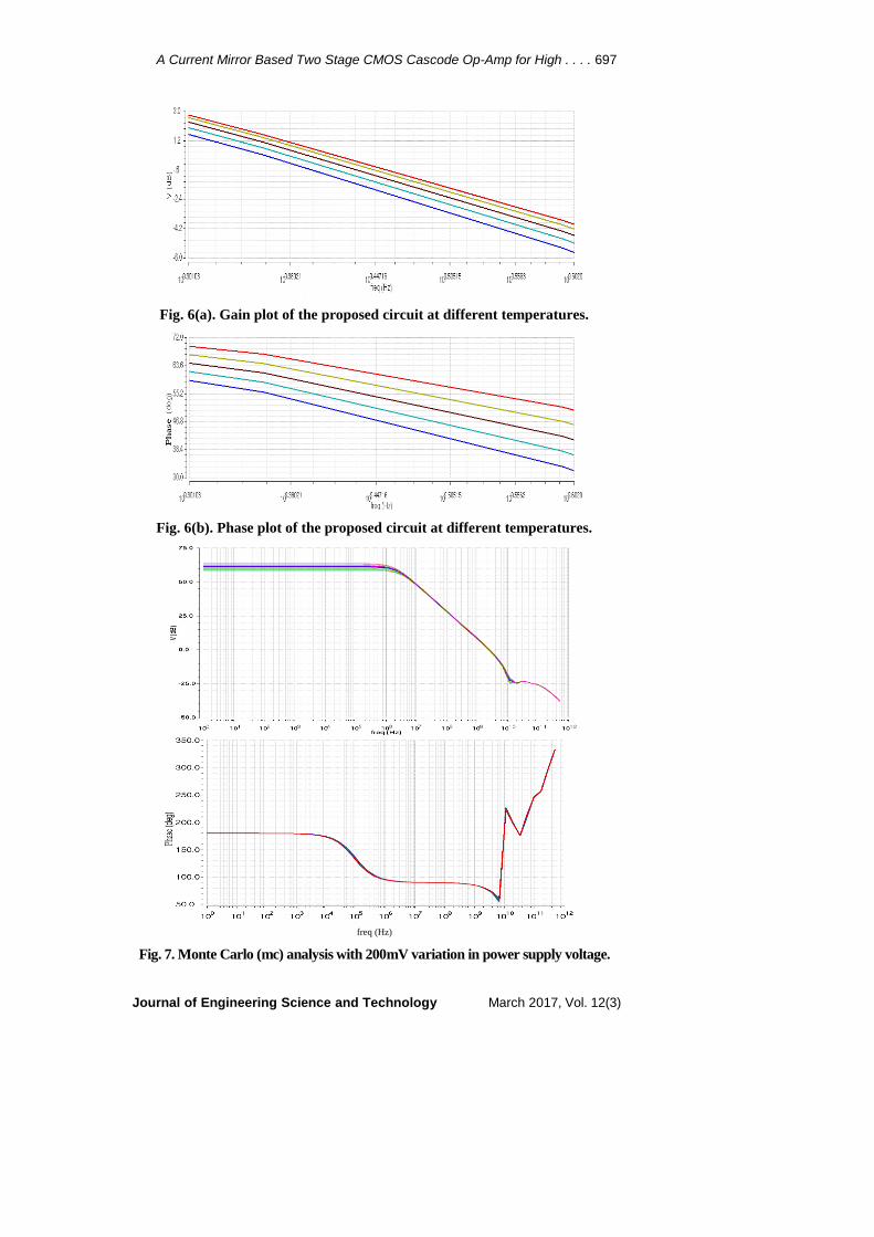
When an op-amp is used for practical applications, the operating
temperature and power supply voltage is variable. Hence it is required for
an op-amp to produce satisfactory results with variations over temperature
and power supply voltage. So, the proposed design has been simulated
at different temperatures and the resulted plot is given in Figs. 6(a) and (b).
The results have also been tabulated in Table 1. From the figure and table
we can observe that as the temperature increases, there is very small
degradation in the performance of the op-amp. The proposed circuit has
been also simulated at different process corners such as Monte Carlo (mc),
typical NMOS and typical PMOS (tt), fast NMOS and fast PMOS (ff),
A Current Mirror Based Two Stage CMOS Cascode Op-Amp for High . . . . 695
Journal of Engineering Science and Technology March 2017, Vol. 12(3)
slow NMOS and slow PMOS (ss), fast NMOS and slow PMOS (fs),
slow NMOS and fast PMOS (sf). The obtained results are tabulated in Table 2.
The result shows that the ff process corner produces the worst result in terms
of gain and UGB. The worst result in terms of phase margin in produced by
sf process corner. Finally, Monte Carlo analysis has been performed
with respect to power supply for maximum variations of 200 mV, which
is given in Fig. 7.
Total Harmonic Distortion (THD) is used to quantify the distortion which is
caused by amplifier non linearity. THD is generally measured in terms of dB or
percentage as outlined in Appendix A. To compare THD of the proposed circuit,
cascoding in the first stage and second stage with respect to output peak to peak
voltages at 1 KHz frequency is given in Fig. 8. As demonstrated in Fig. 8, the
proposed op-amp achieves higher linearity than the op-amp with cascoding in first
stage and second stage. The THD results have been tabulated in Table 3.
For wireless applications, there are need of good gain as well as adequate
UGB and low power consumption. In Table 3, a cross comparative comparison
has been done among CMOS op-amp with cascoding in first stage (Fig. 1),
second stage (Fig. 2) and other previously reported op-amps [10 - 13]. It can be
observed from Table 3 that the performance of the proposed op-amp is better than
CMOS op-amp with cascoding in the first stage and second stage in every aspect.
When compared with the other reported designs, the proposed circuit produces a
higher UGB. In fact the proposed circuit shows very large UGB of 2.70 GHz. The
circuit designed to consume just 710 μW power, which is comparatively very
low. From the results, it can say that the proposed op-amp satisfies all the
requirements for application in wireless application. Finally the layout of the
proposed circuit is shown in Fig. 9 and circuit is verified by design rule check
(DRC), layout versus schematic (LVS) and parasitic extraction (RCX). The pre
layout and post layout simulation gives nearly the same result.
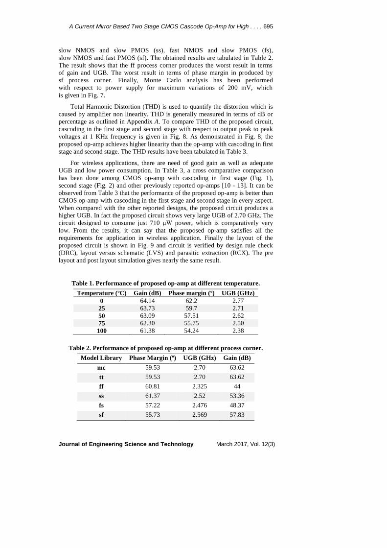
Table 1. Performance of proposed op-amp at different temperature.
Temperature (ºC) Gain (dB) Phase margin (º) UGB (GHz)
0 64.14 62.2 2.77
25 63.73 59.7 2.71
50 63.09 57.51 2.62
75 62.30 55.75 2.50
100 61.38 54.24 2.38
Table 2. Performance of proposed op-amp at different process corner.
Model Library Phase Margin (º) UGB (GHz) Gain (dB)
mc 59.53 2.70 63.62
tt 59.53 2.70 63.62
ff 60.81 2.325 44
ss 61.37 2.52 53.36
fs 57.22 2.476 48.37
sf 55.73 2.569 57.83
696 R. Kundu et al.
Journal of Engineering Science and Technology March 2017, Vol. 12(3)
Table 3. Cross platform comparative performance
Parameters Fig. 1 Fig. 2 [10] [11] [12] [13] This
Work
Technology (nm) 45 45 180 350 65 350 45
Supply Voltage (V) 1.4 1.4 2 3.3 1 3.3 1.4
Gain (dB) 36.86 44.13 60.5 68 56 67 63.62
UGB (GHz) 1.00 1.78 0.065 0.484 0.45 1.25 2.70
Phase Margin (º) 47.8 52 81 68 77 65 59.53
Slew Rate (V/µs) 1107 1678 - 666 - 857 1816
Power Dissipation
(mW)
1.04 1.42 9.5 6.4 1.6 9.5 0.71
THD (V0p-p=1V)
(dB)
-54 50 - -72 - -76 -75
Fig. 5(a). Gain plot of CMOS op-amp with cascoding in first stage,
CMOS op-amp with cascoding in second stage and the proposed circuit.
Fig. 5(b). Phase plot of CMOS op-amp with cascoding in first stage,
CMOS op-amp with cascoding in second stage and the proposed circuit.
A Current Mirror Based Two Stage CMOS Cascode Op-Amp for High . . . . 697
Journal of Engineering Science and Technology March 2017, Vol. 12(3)
Fig. 6(a). Gain plot of the proposed circuit at different temperatures.
Fig. 6(b). Phase plot of the proposed circuit at different temperatures.
freq (Hz)
Fig. 7. Monte Carlo (mc) analysis with 200mV variation in power supply voltage.

698 R. Kundu et al.
Journal of Engineering Science and Technology March 2017, Vol. 12(3)
Fig. 8. THD of the proposed circuit with
respect to peak-to peak output voltage at 1 kHz.
Fig. 9. Layout of the proposed CMOS op-amp
with current mirror based cascoding in second stage.
4. Conclusions
In this paper a novel op-amp design technique has been introduced which uses a
current mirror based cascoding at the second stage of an op-amp. The technique
used here increases the gain-bandwidth product of the op-amp. It has been clearly
stated in this paper that the cascoding technique produces better results than other
cascoding techniques using gain and phase plots. The main advantage of the circuit
is that it produces an overall very good result for wireless applications. Moreover,
this op-amp operates over a wide range of temperature. The gain of the circuit
shows a variation of just 0.02dB/ºC. Also, the variation of power supply voltage has
very little effect on the circuit’s performance. From the THD simulation done with
respect to peak-to-peak output voltage, we can say that the circuit designed is highly
linear circuit. When compared to previously designed circuits, a superior gain,
bandwidth, slew-rate, and power dissipation has been observed in the circuit.

A Current Mirror Based Two Stage CMOS Cascode Op-Amp for High . . . . 699
Journal of Engineering Science and Technology March 2017, Vol. 12(3)
References
1. Valero Bernal, M.R.; Celma, S.; Medrano, N.; and Calvo, B. (2012). A
ultralow-power low voltage class-AB fully differential op-amp for long life
autonomous portable equipment. IEEE Circuit and System Society, 59(10),
643-647.
2. Gangopadhyay, D.; and Bhatacharyya, T.K. (2010). A 2.3 GHz gm- boosted
high swing class AB ultra wide bandwidth operational amplifier in 0.18μm
CMOS. Proceeding of the IEEE 53rd International Midwest Symposium on
Circuit and systems. Seattle, WA, 713-716.
3. Salehi, M.R.; Rezvan Dastanian; Abiri, E.; and Sajad Nejadhasan (2015).
A 147 μW, 0.8 V and 7.5 (mV/V) LIR regulator for UHF RFID application.
International journal of Electronics and Communication (AEU), 69(1),
133-140.
4. Carrillo, J.M.; Perez-Aloe, R.; Valverde, J.M.; and Duque-Carrillo, J.F.
(2009). Compact low-voltage rail to rail bulk driven CMOS op-amp for
scaled technologies. Proceeding of the European Conference on Circuit
Theory and Design. Antalya, Turkey, 263-266.
5. Carrillo, J.M.; Torelli, G.; Perez-Aloe, R.; and Duque-Carrillo, J.F. (2007). 1-
V rail to rail CMOS op-amp with improved bulk driven input stage. IEEE
Journal of Solid -State Circuits, 42(3), 508-517.
6. Raikos, G.; and Vlassis, S. (2010). 0.8V bulk driven operational amplifier.
Analog Integrated Circuits and Signal Processing, 63(3), 425-432.
7. Guo, C.; Zhu, S.; Hu, J.; Zou, J.; Sun, H.; and Lv, X. (2011). A low voltage
CMOS rail to rail operational amplifier based on flipped differential pairs.
Proceeding of the IEEE 4th International Symposium on IEEE Microwave,
Antenna, Propagation and EMC Technologies for Wireless Communications.
Beijing, China, 217-220.
8. Allen, P.E.; and Holberg, D.R. (2011). CMOS analog circuit design (2nd
ed.).
India: Oxford Indian Edition.
9. Gray, P.R.; Hurst, P.J.; Lewis, S.H.; and Meyer, R.G. (2013). Analysis and
Design of Analog Integrated Circuit (5th
ed.). New York: John Wiley and Sons.
10. Ramirez-Angulo, J.; Sawant, M.; Lopez-Martin, A.J.; and Carvajal, R.G.
(2008). A power efficient and simple scheme for dynamically biasing
cascode amplifiers and telescopic op-amps. Integration, the VLSI journal,
41(4), 539-543.
11. Dadashi, A.; Sadrafshari, S.; Hadidi, K.; and Khoei, A. (2011). An enhanced
folded cascode op-amp using positive feedback and bulk amplification in
0.35μm CMOS process. Analog Integrated Circuits and Signal Processing,
67(2), 213-222.
12. Taherzadeh-Sani, M.; and Hamoui, A.A. (2011). A 1-V Process-insensitive
current-scalable two-stage op-amp with enhanced DC gain and settling
behavior in 65-nm Digital CMOS. IEEE Journal Solid-state Circuits, 46(3),
660-668.
13. Dadashi, A.; Sadrafshari, S.; Hadidi, K.; and Khoei, A. (2012). Fast-settling
CMOS op-amp with improved DC-gain. Analog Integrated Circuits and
Signal Processing, 70(3), 283-292.

700 R. Kundu et al.
Journal of Engineering Science and Technology March 2017, Vol. 12(3)
Appendix A
Total Harmonic Distortion
The distortion produced by an amplifier that compares the output signal with the
input signal of amplifier and measures the level differences. The THD is
represented by dB or %. The total harmonic distortion has to be negative because
distortion factor is always less than 1. The amplifier achieves a high linearity, if
THD is more negative in dB.
THD (dB) 100
log20k
D , where k in %.
THD (%) 100.10 20
D
k , where D in dB with a minus sign.