accelerating ml recommendation with over a ... - esperanto.ai
TRANSCRIPT

Accelerating ML Recommendation with over a Thousand
RISC-V/Tensor Processors on Esperanto’s ET-SoC-1 Chip
Dave Ditzel, email: [email protected], Founder and Executive Chairman, Esperanto Technologies,
Roger Espasa, Nivard Aymerich, Allen Baum, Tom Berg, Jim Burr, Eric Hao, Jayesh Iyer, Miquel Izquierdo, Shankar Jayaratnam,
Darren Jones, Chris Klingner, Jin Kim, Stephen Lee, Marc Lupon, Grigorios Magklis, Bojan Maric, Rajib Nath, Mike Neilly, Duane
Northcutt, Bill Orner, Jose Renau, Gerard Reves, Xavier Reves, Tom Riordan, Pedro Sanchez, Sri Samudrala, Guillem Sole,
Raymond Tang, Tommy Thorn, Francisco Torres, Sebastia Tortella, Daniel Yau
Esperanto Technologies Hot Chips 33 Presentation August 24, 2021

2
The ET-SoC-1 is the highest performance commercial RISC-V chip
The ET-SoC-1 has over a thousand RISC-V processors on a single TSMC 7nm chip, including:
• 1088 energy-efficient ET-Minion 64-bit RISC-V in-order cores each with a vector/tensor unit
• 4 high-performance ET-Maxion 64-bit RISC-V out-of-order cores
• >160 million bytes of on-chip SRAM
• Interfaces for large external memory with low-power LPDDR4x DRAM and eMMC FLASH
• PCIe x8 Gen4 and other common I/O interfaces
• Innovative low-power architecture and circuit techniques allows entire chip to
• Compute at peak rates of 100 to 200 TOPS
• Operate using under 20 watts for ML recommendation workloads
This general-purpose parallel-processing system on a chip can be used for many parallelizable workloads
But today, we want to show why it is a compelling solution for Machine Learning Recommendation (inference)
• ML Recommendation is one of the hardest and most important problems for many hyperscale data centers

3
Requirements and challenges for ML Recommendation in large datacenters
Most inferencing workloads for recommendation systems in large data centers are run on x86 servers
Often these servers have an available slot for an accelerator card, but it needs to meet key requirements:
• 100 TOPS to 1000 TOPS peak rates to provide better performance than the x86 host CPU alone
• Limited power budget per card, perhaps 75 to 120 watts, and must be air-cooled[1]
• Strong support for Int8, but must also support FP16 and FP32 data types[1,2]
• ~100 GB of memory capacity on the accelerator card to hold most embeddings, weights and activations[3]
• ~100 MB of on-die memory[5]
• Handle both dense and sparse compute workloads. Embedding look-up is sparse matrix by dense matrix
multiplication[5]
• Be programmable to deal with rapidly evolving workloads[1], rather than depending on overly-specialized
hardware[4,5]

4
Esperanto’s approach is different... and we think better for ML Recommendation
Other ML Chip approaches
One Giant Hot Chip uses up power budget
Limited I/O pin budget limits memory BW
Dependence on systolic array multipliers
• Great for high ResNet50 score
• Not so good with large sparse memory
Only a handful (10-20) of CPU cores
• Limited parallelism with CPU cores when
problem doesn’t fit onto array multiplier
Standard voltage: Not energy efficient
Use multiple low-power chips that still fit within power budget
Performance, pins, memory, bandwidth scale up with more chips
Thousands of general-purpose RISC-V/tensor cores
• Far more programmable than overly-specialized (eg systolic) hw
• Thousands of threads help with large sparse memory latency
Full parallelism of thousands of cores always available
Low-voltage operation of transistors is more energy-efficient
• Lower voltage operation also reduces power
• Requires both circuit and architecture innovations
DRAM
Esperanto’s better approach
DRAM DRAM DRAM DRAM DRAM DRAM
> 1000
RISC-V/Tensor
Cores
> 1000
RISC-V/Tensor
Cores
> 1000
RISC-V/Tensor
Cores
> 1000
RISC-V/Tensor
Cores
> 1000
RISC-V/Tensor
Cores
> 1000
RISC-V/Tensor
Cores
Challenge: How to put the highest ML Recommendation performance
onto a single accelerator card with a 120-watt limit?
10-20 CPU cores
and
Systolic Array Multipliers

5
Could fit six chips on 120W card, if each took less than 20 watts
Assumed half of 20W power for 1K RISC-V cores, so only 10 mW per core!
Power (Watts) = Cdynamic x Voltage2 x Frequency + Leakage
Power/core Frequency Voltage Cdynamic
Generic x86 Server core (165W for 24 cores) 7 W 3 GHz 0.850v 2.2nF
10mW ET-Minion core (~10W for 1K cores) 0.01 W 1 GHz 0.425v 0.04nF
Reductions needed to hit goals ~700x 3x 4x 58x
Easy Hard
Circuit/SRAMVery Hard
Architecture

6
Re
co
mm
en
da
tio
n E
ne
rgy E
ffic
ien
cy
of E
T-M
inio
n c
ore
s (
Infe
ren
ce
s/S
ec/W
att)
Study of energy-efficiency and number of chips to get best ML Performance in 120 watts[6]
Operating voltage for the 1K ET-Minion RISC-V/Tensor cores
Esperanto’s
sweet-spot for
best performance
0.2 0.3 0.4 0.5 0.6 0.7 0.8 0.9
20 W6 chips
275 W1 chip
4x better ML
recommendation
performance
2.5x better performance than the 118W chip20x better Energy-Efficiency
by using lowest voltage instead of
highest voltage for our
recommendation benchmark
8.5 W
6 chips

7
DC bank 0 DC bank 1 DC bank 2 DC bank 3
Data Cache Control
(including D-tags) Front
End
Trans
ROMs
32-bit & 16-bit FMA Bypass TIMA TIMA VPU RF T0/T1
VPU RF T0/T1
32-bit & 16-bit FMA Bypass TIMA TIMA VPU RF T0/T1
32-bit & 16-bit FMA Bypass TIMA TIMA VPU RF T0/T1 Trans
ROMs
32-bit & 16-bit FMA Bypass TIMA TIMA
Trans
ROMs
32-bit & 16-bit FMA Bypass TIMA TIMA VPU RF T0/T1
VPU RF T0/T1
32-bit & 16-bit FMA Bypass TIMA TIMA VPU RF T0/T1
32-bit & 16-bit FMA Bypass TIMA TIMA VPU RF T0/T1 Trans
ROMs
32-bit & 16-bit FMA Bypass TIMA TIMA
ET-Minion is an Energy-Efficient RISC-V CPU with a Vector/Tensor Unit
512b Int8
RISC-V Integer Pipeline
Ve
cto
r/T
enso
r U
nit
256b Floating Point Vector RF
ET-Minion RISC-V Core and Tensor/Vector unit
optimized for low-voltage operation
to improve energy-efficiency
RIS
C-V
In
teg
er
L1 Data-Cache/Scratchpad
Optimized for energy-efficient ML operations. Each ET-Minion can deliver peak of 128 Int8 GOPS per GHz
ET-MINION IS A CUSTOM BUILT 64-BIT RISC-V PROCESSOR• In-order pipeline with low gates/stage to improve MHz at low voltages
• Architecture and circuits optimized to enable low-voltage operation
• Two hardware threads of execution
• Software configurable L1 data-cache and/or scratchpad
ML OPTIMIZED VECTOR/TENSOR UNIT• 512-bit wide integer per cycle
• 128 8-bit integer operations per cycle, accumulates to 32-bit Int
• 256-bit wide floating point per cycle
• 16 32-bit single precision operations per cycle
• 32 16-bit half precision operations per cycle
• New multi-cycle Tensor Instructions
• Can run for up to 512 cycles (up to 64K operations) with one tensor instruction
• Reduces instruction fetch bandwidth and reduces power
• RISC-V integer pipeline put to sleep during tensor instructions
• Vector transcendental instructions
OPERATING RANGE: 300 MHz TO 2 GHz

8
8 ET-Minions form a “Neighborhood”
NEIGHBORHOOD CORES WORK CLOSELY TOGETHER
• Architecture improvements capitalize on physical proximity of 8 cores
• Take advantage that almost always running highly parallel code
OPTIMIZATIONS FROM CORES RUNNNING THE SAME CODE
• 8 ET-Minions share single large instruction cache,
this is more energy efficient than many separate instruction caches.
• “Cooperative loads” substantially reduce memory traffic to L2 cache
NEW INSTRUCTIONS MAKE COOPERATION MORE EFFICIENT
• New Tensor instructions dramatically cut back on instruction fetch bandwidth
• New instructions for fast local synchronization within group
• New Send-to-Neighbor instructions
• New Receive-from-Neighbor instructions
ET-Minion 0
ET-Minion 1
ET-Minion 2
ET-Minion 3
ET-Minion 4
ET-Minion 5
ET-Minion 6
ET-Minion 7
32
KB
sh
are
d
Ins
tru
cti
on
Ca
ch
e

9
32 ET-Minion CPUs and 4 MB Memory form a “Minion Shire”
32 ET-MINION RISC-V CORES PER MINION SHIRE• Arranged in four 8-core neighborhoods
SOFTWARE CONFIGURABLE MEMORY HIERARCHY
• L1 data cache can also be configured as scratchpad
• Four 1MB SRAM banks can be partitioned as private L2,
shared L3 and scratchpad
SHIRES CONNECTED WITH MESH NETWORK
NEW SYNCHRONIZATION PRIMITIVES
• Fast local atomics
• Fast local barriers
• Fast local credit counter
• IPI support
4x4
xbar
Mesh
stop
m0m3
m4m7
m8m11
m12m15
m16m19
m20m23
m24m27
m28m31
Minion
Shire
Bank0
(1MB)
Bank1
(1MB)
Bank2
(1MB)
Bank3
(1MB)
Four 8-Core
Neighborhoods
4MB Banked SRAM
Cache/Scratchpad
Local Sync Primitives
Mesh
Interconnect
Low Voltage
Nominal Voltage
Low Voltage

10
4x4
xbar
Mesh
stop
m0m3
m4m7
m8m11
m12m15
m16m19
m20m23
m24m27
m28m31
Bank0
(1MB)
Bank1
(1MB)
Bank2
(1MB)
Bank3
(1MB)
4x4
xbar
Mesh
stop
m0m3
m4m7
m8m11
m12m15
m16m19
m20m23
m24m27
m28m31
Bank0
(1MB)
Bank2
(1MB)
Bank3
(1MB)
Bank1
(1MB)
4x4
xbar
Mesh
stop
m0m3
m4m7
m8m11
m12m15
m16m19
m20m23
m24m27
m28m31
Bank0
(1MB)
Bank1
(1MB)
Bank2
(1MB)
Bank3
(1MB)
4x4
xbar
Mesh
stop
m0m3
m4m7
m8m11
m12m15
m16m19
m20m23
m24m27
m28m31
Bank0
(1MB)
Bank1
(1MB)
Bank2
(1MB)
Bank3
(1MB)
Shires are connected to each other and to external memory through Mesh Network
Minion Shire
Minion Shire
Minion Shire
Minion Shire

11
ET-SoC-1: Full chip internal block diagram
Block diagram of Esperanto’s energy-efficient ET-SoC-1 chip
16-bits
16-bits
MEMORY SHIRE
LPDDR4x
controller
LPDDR4x
controller
16-bits
16-bits
MEMORY SHIRE
LPDDR4x
controller
LPDDR4x
controller
16-bits
16-bits
MEMORY SHIRE
LPDDR4x
controller
LPDDR4x
controller
16-bits
16-bits
MEMORY SHIRE
LPDDR4x
controller
LPDDR4x
controller
16-bits
16-bits
MEMORY SHIRE
LPDDR4x
controller
LPDDR4x
controller
16-bits
16-bits
MEMORY SHIRE
LPDDR4x
controller
LPDDR4x
controller 16-bits
16-bits
MEMORY SHIRE
LPDDR4x
controller
LPDDR4x
controller
16-bits
16-bits
MEMORY SHIRE
LPDDR4x
controller
LPDDR4x
controller
PCIe SHIRE MAXION / IO SHIRE
MINION
SHIRE
MINION
SHIREMINION
SHIRE
MINION
SHIRE
MINION
SHIREMINION
SHIRE
ET-Maxion
ET-Maxion ET-Maxion
ET-Maxion
RISC-V Service
Processor
PCIe logic DFT/eFuses
MINION
SHIRE
MINION
SHIREMINION
SHIRE
MINION
SHIRE
34 MINION SHIRES
• 1088 ET-Minions
8 MEMORY SHIRES• LPDDR4x DRAM
controllers
1 MAXION / IO SHIRE
• 4 ET-Maxions
• 1 RISC-V Service
Processor
PCIe SHIRE
160 million bytes of
on-die SRAM
x8 PCIe Gen4
Secure Root of Trust

12
ET-SoC-1 External Chip Interfaces
8-bit PCIe Gen4
• Root/endpoint/both
256-bit wide LPDDR4x
• 4267 MT/s
• 137 GB/s
• ECC support
RISC-V SERVICE PROCESSOR
• Secure Boot
• System Management
• Watchdog timers
• eFuse
EXTERNAL IO
• SMBus
• Serial – I2C/SPI/UART
• GPIO
• FLASH

13
PCIe switch
ET-SoC-11088 ET-Minions
4 ET-Maxions
160 MB SRAM
ET-SoC-11088 ET-Minions
4 ET-Maxions
160 MB SRAM
ET-SoC-11088 ET-Minions
4 ET-Maxions
160 MB SRAM
ET-SoC-11088 ET-Minions
4 ET-Maxions
160 MB SRAM
ET-SoC-11088 ET-Minions
4 ET-Maxions
160 MB SRAM
ET-SoC-11088 ET-Minions
4 ET-Maxions
160 MB SRAM
LP
DD
R4x
4 1
6-b
it c
hannels
LP
DD
R4x
4 1
6-b
it c
hannels
LP
DD
R4x
4 1
6-b
it c
hannels
LP
DD
R4x
4 1
6-b
it c
hannels
LP
DD
R4x
4 1
6-b
it c
hannels
LP
DD
R4x
4 1
6-b
it c
hannels
LP
DD
R4x
4 1
6-b
it c
hannels
LP
DD
R4x
4 1
6-b
it c
hannels
LP
DD
R4x
4 1
6-b
it c
hannels
LP
DD
R4x
4 1
6-b
it c
hannels
LP
DD
R4x
4 1
6-b
it c
hannels
LP
DD
R4x
4 1
6-b
it c
hannels
LP
DD
R4x
4 1
6-b
it c
hannels
LP
DD
R4x
4 1
6-b
it c
hannels
LP
DD
R4x
4 1
6-b
it c
hannels
LP
DD
R4x
4 1
6-b
it c
hannels
LP
DD
R4x
4 1
6-b
it c
hannels
LP
DD
R4x
4 1
6-b
it c
hannels
LP
DD
R4x
4 1
6-b
it c
hannels
LP
DD
R4x
4 1
6-b
it c
hannels
LP
DD
R4x
4 1
6-b
it c
hannels
LP
DD
R4x
4 1
6-b
it c
hannels
LP
DD
R4x
4 1
6-b
it c
hannels
LP
DD
R4x
4 1
6-b
it c
hannels
PCIe card interface
Card with six ET-SOC-1 chips for large sparse ML Recommendation models
• Esperanto’s low-power technology allows six Esperanto chips and 24 DRAM chips to fit into120-Watt power budget of customer’s PCIe card
• A single ML model on one accelerator card can use up to 192 GB of low-cost LPDDR4x DRAM with up to 822 GB/s of memory bandwidth
• Over 6K cores with 12K threads handles memory latency on 96 memory channels and performs well for ML Recommendation (and other) tasks
96 1
6-
bit c
han
ne
ls
1536-bit wide memory system
Up to 192 GB of accelerator memory with 24 DRAMs each 64-bits wide.
Esperanto can handle large memory requirements for ML Recommendation.
24 D
RA
M c
hip
s

14
Six ET-SoC-1 chips fit on an OCP Glacier Point v2 Card
Based on the open-source Glacier Point v2 board
design from the Open Compute Project.
Three Esperanto Dual M.2 modules can mount on the
top side and three on the bottom side.
Peak performance > 800 TOPS8 when all ET-Minions on six chips are operating at 1 GHz
GLACIER POINT V2 CARD SHOWN:• 6,558 RISC-V cores
• Up to 192 GB of DRAM
• Up to 822 GB/s DRAM bandwidth
• ~120 W maximum power consumption
ON OTHER PCI EXPRESS CARDS:• One ET-SoC-1 fits easily on a Low-Profile
(half-height, half-length) PCIe add-in card
• ET-SoC-1 power budget increases to ~60W
• Many PCIe cards can be operated in parallel

15
OCP Glacier Point v2
accelerator card
holds:
• 6 Esperanto
ET-SoC-1 chips
Yosemite v2 Cubby
holds:
• 4 Yosemite Sleds
• 8 accelerator cards
• 48 ET-SoC-1 chips
Example OCP Data Center
holds:
@ 30 sq. ft. per OCP rack [7]
Estimated 4K-20K racks / data center
Millions of ET-SoC-1 chips
Rack with Yosemite v2
holds:
8 Yosemite v2 Cubbies
64 accelerator cards
384 ET-SoC-1 chips
Yosemite v2 Sled
holds:
• 2 Glacier Point v2
accelerator cards
• 12 ET-SoC-1 chips
Yo
sem
ite v
2
x4 x8
ET-SoC-1 can be deployed at scale in existing OCP Data Centers
x2Top of Rack Switch
Power Shelf
Power Shelf

16
Software: Esperanto Supports C++ / PyTorch and Common ML Frameworks
Development Tools
Management Utilities
GLOW/TVM driver runs on x86 host
ML Models run across multiple
ET-SoC-1 chips
ML Model Frameworks
Console /
DebuggerPerformance
MonitorGLOW/TVM Frontend:
GLOW = Graph LOWering
Open source graph compilers
Hardware-independent optimizations
Divides work across N chips
GLOW/TVM Backend:
Does hardware-dependent optimizations
Backend modified by ET to generate
instructions for ET-SoC-1 chipDiagnostics
Firmware
Updater
. . .
…..
ONNX Models
MS CNTK
GLOW
ET RISC-V Code Gen
ET-Runtime
ET PCIe Driver
C++
ET-GLOW Backend
TVM
LLVM
…..

17
1
11
31
59
1
39
52
123
0
25
50
75
100
125
Intel 8380H NVIDIA T4 NVIDIA A10 ET-SOC-1 x6
ML Recommendation performance per card comparisonsBased on MLPerf Deep Learning Recommendation Model benchmark [8]
NVIDIA A10
772,378 with 8 A10 cards[9c]
1200 watts for 8 A10
96,547 Samples/sec/A10 card
150 watts per A10 card
Esperanto ET-SoC-1
182,418 with 1 card (6 chips) [9d]
120 watts
182,418 Samples/sec/card
120 watts per card
= Relative Performance (Samples/Second)
= Relative Energy Efficiency (Samples/Second/Watt)
or Relative Performance at equal Power
Esperanto estimates[9d]
123x better
performance per watt
Intel Xeon Platinum 8380H 8S
24,630 Samples/sec with 8 die [9a.1]
2000 watts for 8 die
3,079 Samples/sec/die
250 watts per die [9a.2]
NVIDIA T4
665,646 with 20 T4 cards [9b]
1400 watts for 20 T4
33,282 Samples/sec/T4 card
70 watts per T4 card
MLPerf DLRM results for Intel and NVIDIA from MLCommons website[8], power numbers from data sheets.

18
1.02.0
3.9
7.6
15.4
1.0
5.7 5.3
15.2
25.7
0
5
10
15
20
25
30
Image Classification performance per card comparisonsBased on ResNet-50 benchmark [10]
= Relative Performance (Inferences/Second)
= Relative Energy Efficiency
(Inferences/Second/Watt)
or Relative Performance at equal Power
Intel Xeon Platinum 9282 2S
(4 die @200W TDP each[10a.2])
7,878 Inf/sec batch size=11[10a.1]
1,970 Inferences/sec/die
200 watts per die
NVIDIA T4
(1 die @70W TDP)
batch size=8
3,920 Inferences/sec[10b]
70 watts per card
Esperanto ET-SoC-1
6 die (@20W each)
batch size=8
30,369 Inferences/sec[10d]
120 watts per card
NVIDIA A10
(1 die @150W TDP)
batch size=8
7,755 Inferences/sec[10b]
150 watts per card
Habana Goya
(1 die @100W)
batch size=10
15,012 Inferences/sec[10c]
100 watts per card
25.7x better
performance per watt
Esperanto estimatesResNet-50 numbers taken from respective company websites, power numbers from data sheets.

19
Four ET-Maxions: High-Performance Out-of-Order RISC-V Processors
FULL RISC-V RV64GC ISA SUPPORT
• Support for compressed ISA
• Privileged ISA
• Fully respects relaxed consistency model
SUPPORTS 4 CORE SMP LINUX OS
• Allows chip to run in standalone configuration
OUT-OF-ORDER EXECUTION
• 64-entry distributed scheduler
• 128-entry ROB
• 32-entry load queue, 32-entry store queue
• 8R/4W 128-entry integer physical register file
• 3R/2W 64 floating-point physical register file
• Execution units:
• 1 load/store, 2 simple ALU, 1 complex ALU/Branch, 1 FP
MEMORY SUB-SYSTEM
• 32 entry data and instruction TLBs and 512 entry unified L2 TLB
• Fully coherent 64KB data cache backed by a unified 4MB L2 cache
• ECC for both data and L2 caches
• Aggressive stride prefetchers for L1 and L2 data caches
OPERATING RANGE: 500 MHz to 2 GHz
For details on ET-Maxion,
see references [11,12]
20
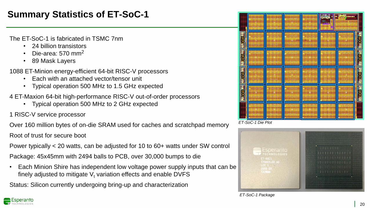
Summary Statistics of ET-SoC-1
The ET-SoC-1 is fabricated in TSMC 7nm
• 24 billion transistors
• Die-area: 570 mm2
• 89 Mask Layers
1088 ET-Minion energy-efficient 64-bit RISC-V processors
• Each with an attached vector/tensor unit
• Typical operation 500 MHz to 1.5 GHz expected
4 ET-Maxion 64-bit high-performance RISC-V out-of-order processors
• Typical operation 500 MHz to 2 GHz expected
1 RISC-V service processor
Over 160 million bytes of on-die SRAM used for caches and scratchpad memory
Root of trust for secure boot
Power typically < 20 watts, can be adjusted for 10 to 60+ watts under SW control
Package: 45x45mm with 2494 balls to PCB, over 30,000 bumps to die
• Each Minion Shire has independent low voltage power supply inputs that can be
finely adjusted to mitigate Vt variation effects and enable DVFS
Status: Silicon currently undergoing bring-up and characterization
ET-SoC-1 Die Plot
ET-SoC-1 Package

21
Summary
The Esperanto ET-SoC-1 is the highest performance commercial RISC-V chip to date• More RISC-V cores on a single chip
• More RISC-V aggregate instructions per second on a single chip
• Highest TOPS driven by RISC-V cores
Esperanto’s low-voltage technology provides differentiated RISC-V processors with the best performance per watt• Energy efficiency matters!
• Best performance per watt delivers the best performance in a fixed number of watts
• Solution delivers energy efficient acceleration for datacenter inference workloads, especially recommendation
The hard part was making all the tradeoffs combining• Processor and memory system architecture
• Circuits and techniques for low voltage operation
Esperanto now has a highly scalable design• Efficient for ML recommendation
• Thousands of general-purpose RISC-V cores can be applied to many other highly parallel computing tasks
• Modular approach allows design to scale up and down, and to other semiconductor processes
Early Access Program for qualified customers beginning later in 2021 (for info, contact: [email protected])

22
Thanks to our Key Development Partners
Thanks to all our partners for their help in bringing our vision into reality! Sorry we can’t name
everyone!

23
Footnotes and References
[1] N. Jouppi, et al., Ten Lessons from Three Generations Shaped Google’s TPUv4i, 2021 ACM/IEEE 48th Annual International Symposium on Computer Architecture. Page 4 lesson 5 concludes “Inference
DSAs need air cooling for global scale”.
[2] J. Park, et al., Deep Learning Inference in Facebook Data Centers: Characterization, Performance Optimizations and Hardware Implications, arXiv:1811.09886v2, 29 November 2018.
[3] M. Anderson, et al., First Generation Inference Accelerator Deployment at Facebook, arXiv: 2107.04140v1, 8 Jul 2021
[4] M. Smelyanskiy, Facebook, Linley Fall Processor Conference 2019 “Challenges and Opportunities of Architecting AI Systems at Datacenter Scale”
[5] M. Smelyanskiy, AI System Co-Design: How to Balance Performance & Flexibility, AI Hardware Summit, September 17, 2019. Slide 12 indicated desired Inference characteristics with 100 TOPs of INT8,
100 MB of SRAM. Slide 19 talks about the need for programmability over fixed function hardware.
[6] Note that a core optimized for high voltage and high frequency (2-3GHz) operation will require higher power gate drive strengths to overcome wire delays and hence will have higher Cdyn than a processor
optimized for low-voltage operation. Each of the power/frequency points shown on this energy efficiency curve therefore represents a different physical design, i.e. not the same silicon, to take this changing
Cdyn into account. Designs were synthesized at high and low voltages to estimate potentially achievable frequencies. Performance at each frequency was estimated using our internal ML Recommendation
benchmark, based on running this benchmark on a full chip hardware emulation engine (Synopsys Zebu system) providing clock level accuracy at a few points and interpolating the other points. The goal was
to understand the shape of the energy efficiency curve to find voltages for best energy efficiency (Inferences/second/watt). Different benchmarks would likely have different curves, though we would expect the
overall shape to be similar. Repeating, this was a design study and does not represent any specific silicon results or design, each point on the curve is a differently synthesized design, though with the same
architecture, i.e., we used the full ET-Minion as the input to be synthesized.
[7] Estimate of 30 square feet per rack comes from “The Case for the Infinite Data Center” – Gartner, Source: Gartner, Data Center Frontier
[8] MLPerf DLRM Inference Data Center v0.7 & v1.0: https://mlcommons.org/en/
[9] Measured by MLPerf DLRM Samples / Second; FP32, Offline scores
Additional source information:• a.1. Submitter: Intel; MLPerf DLRM score 24,630: Inference Data Center v0.7 ID 0.7-126; Hardware used (1-node-8S-CPX-PyTorch-BF16); BF16; https://mlcommons.org/en/inference-datacenter-07/
• a.2 Intel 8380H Processor TDP Power of 250W from: https://ark.intel.com/content/www/us/en/ark/products/204087/intel-xeon-platinum-8380h-processor-38-5m-cache-2-90-ghz.html
• b. Submitter: NVIDIA; T4 MLPerf DLRM score 665,646: Inference Data Center v0.7 ID 0.7-115; Hardware used (Supermicro 6049GP-TRT-OTO-29 (20x T4, TensorRT)); INT8; https://mlcommons.org/en/inference-datacenter-07/
• c. Submitter: NVIDIA; A10 MLPerf DLRM score 772,378: Inference Data Center v1.0 ID 1.0-54; Hardware used (Supermicro 4029GP-TRT-OTO-28 (8x A10, TensorRT)); INT8; https://mlcommons.org/en/inference-datacenter-10/
• d. Internal estimates by Esperanto for MLPerf DLRM: Inference Data Center v0.7; ET-SOC-1; Unverified result is from Emulated/Simulated pre-silicon projections; INT8; Result not verified by MLCommons™ Association.
[10] Measured by ResNet-50 Images per second (Esperanto INT8 Batch 8, NVIDIA INT8 Batch 8, Habana INT8 Batch 10, Intel INT8 Batch 11)
Additional measurement source information: • a.1. Intel ResNet-50: https://software.intel.com/content/www/us/en/develop/articles/intel-cpu-outperforms-nvidia-gpu-on-resnet-50-deep-learning-inference.html
• a.2. Intel 9282 has 2 die in the package, CPU TDP power for both die from: https://ark.intel.com/content/www/us/en/ark/products/194146/intel-xeon-platinum-9282-processor-77m-cache-2-60-ghz.html
• b. NVIDIA (T4, A10) ResNet-50: https://developer.nvidia.com/deep-learning-performance-training-inference
• c. Habana ResNet-50: https://habana.ai/wp-content/uploads/2018/09/Goya-Datasheet-HL-10x-Nov14-2018.pdf
• d. Esperanto ResNet-50: Emulated/Simulated projections; INT8
[11] P. Xekalakis and C. Celio, The Esperanto ET-Maxion High Performance Out-of-Order RISC-V Processor, 2018 RISC-V Summit, presentation at https://www.youtube.com/watch?v=NjEslX_-t0Q
[12] Maxion is described in “Esperanto Maxes out RISC-V - High-End Maxion CPU Raises RISC-V Performance Bar”, Microprocessor Report, December 10, 2018.