a high speed cmos a/d converter - nasa · pdf filethe converter uses a novel comparator...
TRANSCRIPT
4th NASA Symposium on VLSI Design 1992 ™ * ' ^ " " / & J i £ , 6 O 8.3.1
A High Speed CMOS A/D Converter1
Don R. Wiseman and Sterling R. WhitakerNASA Space Engineering Research Center
University of New Mexico2650 Yale SE, Suite # 101
Albuquerque, New Mexico 87106
Abstract - This paper presents a high speed A/D converter. The converter is a7 bit flash converter with one half LSB accuracy. Typical parts will function atapproximately 200 MHz. The converter uses a novel comparator circuit that isshown to out perform more traditional comparators, and thus increases the speedof the converter. The comparator is a clocked, precharged circuit that offers veryfast operation with a minimal offset voltage (2 mv). The converter was designedusing a standard 1 micron digital CMOS process and is 2,244 microns by 3,972microns.
1 Introduction
Today, large integrated circuits (ICs) are involved in solving complex signal processing prob-lems. A mixture of digital and analog signals often must be integrated into a single system[1]. Modern digital-to-analog (D/A) and analog-to-digital (A/D) converters have becomecommon components for integrated signal processing. Of the many styles of A/D convertersavailable [l]-[2], only three [3, 4], the flash, half flash, and successive approximation, takefull advantage of the speed that CMOS technologies can provide.
Of the three types of converters, the flash converters are clearly the fastest, but they arealso the largest. For high performance systems, the flash converter is, however, the choice.To minimize the area required this coverter was designed for 7 bits of resolution, thus limitingthe comparator chain to the length of 128 comparator cells. Secondly, the comparator cellitself is highly optimized for both performance and size [5]. Finally, the state of the artprocess used to manufacture this converter will allow 1 micron gate lengths, thus helping tokeep the size of the individual transistors to a minimum.
The basic configuration of a flash A/D converter is shown in Figure 1. This type of A/Dconverter is fully parallel, since it processes each of the n output bits simultaneously thusaccounting for the speed of operation [6]. However, the price for this speed is the require-ment for 2n comparators. Thus, for large values of n this can make flash A/D convertersprohibitively large.
This style of converter works by first taking a reference voltage (Vref) and dividing itdown a chain of resistors. The voltage at each resistor is fed to a comparator, and is comparedwith the input voltage (Vin). Thus the output down the chain of comparators will be a logiczero until the divided reference voltage is less than the input voltage. At that point, andfurther down the comparator string, the outputs will be a logic one. The outputs of the
1This research was supported in part by NASA under Space Engineering Research Center Grant NAGW-1406.
https://ntrs.nasa.gov/search.jsp?R=19940017253 2018-05-09T15:31:30+00:00Z

8.3.2
Vref Vin
R/2
2n
J_ Comparators
2" + 1Resistors
2"Latches
nOutput Bits
Figure 1: Flash A/D converter
comparators are then latched into flip-flops so that comparison of the next input samplemay begin, without destroying the results of the previous conversion. The outputs of theflip-flops are fed into a 2n to n encoder. This encoder is essentially a set of XOR (ExclusiveOr) gates and a small ROM (Read Only Memory) that determines the n binary output bitsgiven the sequence of m zeros and 2n — m ones. Finally, the output from the encoder is sentto a set of output buffers, and the digital representation of the input sample is output fromthe converter [3, 7].
2 Circuit Design
MOSIS will be used to fabricate this part using Hewlett-Packard's CMOS-34 process. CMOS-34 is a single poly, double metal layer process with 1 micron minimum gate lengths. UsingCMOS-34 design rules, this A/D converter was designed to perform at a worst case of 100MHz. To make the digital logic sections of the converter function as fast as possible, pre-charged logic was used in the memory section of the converter. Additionally, a pipelinedarchitecture was implemented throughout the part to assist in increasing circuit speed. Adiagram of the basic structure a flash A/D converter can be seen in Figure 1.
This A/D converter was designed for a 6 volt analog voltage supply and a 5 volt digitalsupply. This results in a maximum analog input voltage swing of 5 volts. With a 5 volt swingpossible at the analog input, each successive count of digital output represents approximately40 mV of change on the input voltage.

4th NASA Symposium on VLSI Design 1992 8.3.3
Digital
Output
111
110
101
100
Oil
010
001
000
I7"~ '
Fr-'A r.J/ ry r.j/ \A \
^A Unset .brror
^d r.JX \
Analog Input
Figure 2: Offset Error Example
2.1 Accuracy Considerations
Before designing an analog integrated circuit, it is necessary to have an understanding of thetypes and sources of possible inaccuracies in the analog to digital conversion. In the worstcase, a sum of all these errors should not result in either circuit failure, or skewed output ofmore than one half of a least significant bit (LSB), 20 mV.
The first type of error that can occur is called offset error. Offset error occurs when theanalog input voltage for each digital step output is in error by a fixed amount. Pictured inFigure 2, offset error is most commonly caused by a uniform offset voltage being present onthe inputs of all of the comparators. The comparators used in this design have a simulatedoffset voltage of less than 2 mV. Therefore, offset voltage problems should be reasonable. Todetermine the offset voltage of the comparators simulations were created that decreased thedifferential input voltage until the comparator failed.
The analog input voltage difference between two digital output steps is ideally one LSB.The difference from this ideal is called differential linearity error. This type of error, pic-tured in Figure 3, can be caused by systematic or random offsets in the comparators, or byresistance mismatches in the resistor chain. If differential errors are large enough, the A/Dconverter can lose its monotonicity. Monotonicity is the characteristic that there is a uniqueinput voltage for each and every digital output word, and that the digital output alwaysincreases for increasing analog input voltages [3].
Another error that can occur in flash A/D converters is integral linearity error. Alsopicture in Figure 3, this error represents a summation of the differential errors up to anypoint in the digital output. Because of this, integral linearity errors generally have the samesources as differential linearity errors [3]. The measures taken to reduce these errors arediscussed throughout the remainder of this paper.
8.3.4
111110101
Digital 10°
Output 011
010
001
000
A/ i
// .
/ « — *| Integral Error/Ug ,j )
/ . ' < Differential
/ i •* ) Errors
/ \/ i
/i/ i
Analog Input
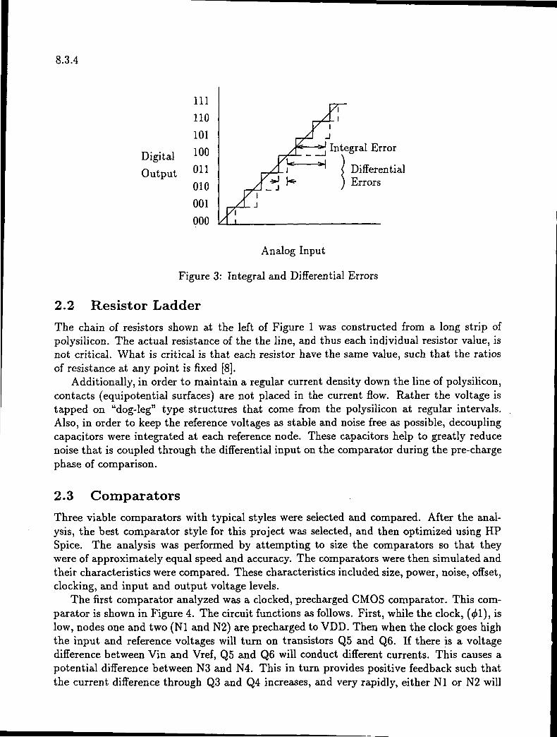
Figure 3: Integral and Differential Errors
2.2 Resistor Ladder
The chain of resistors shown at the left of Figure 1 was constructed from a long strip ofpolysilicon. The actual resistance of the the line, and thus each individual resistor value, isnot critical. What is critical is that each resistor have the same value, such that the ratiosof resistance at any point is fixed [8].
Additionally, in order to maintain a regular current density down the line of polysilicon,contacts (equipotential surfaces) are not placed in the current flow. Rather the voltage istapped on "dog-leg" type structures that come from the polysilicon at regular intervals.Also, in order to keep the reference voltages as stable and noise free as possible, decouplingcapacitors were integrated at each reference node. These capacitors help to greatly reducenoise that is coupled through the differential input on the comparator during the pre-chargephase of comparison.
2.3 Comparators
Three viable comparators with typical styles were selected and compared. After the anal-ysis, the best comparator style for this project was selected, and then optimized using HPSpice. The analysis was performed by attempting to size the comparators so that theywere of approximately equal speed and accuracy. The comparators were then simulated andtheir characteristics were compared. These characteristics included size, power, noise, offset,clocking, and input and output voltage levels.
The first comparator analyzed was a clocked, precharged CMOS comparator. This com-parator is shown in Figure 4. The circuit functions as follows. First, while the clock, (<^1), islow, nodes one and two (Nl and N2) are precharged to VDD. Then when the clock goes highthe input and reference voltages will turn on transistors Q5 and Q6. If there is a voltagedifference between Vin and Vref, Q5 and Q6 will conduct different currents. This causes apotential difference between N3 and N4. This in turn provides positive feedback such thatthe current difference through Q3 and Q4 increases, and very rapidly, either Nl or N2 will

4th NASA Symposium on VLSI Design 1992 8.3.5
VN9
<kh
N7
QisJHV
NlQ7
N3
will—2
N4
r TVref
'T
Figure 4: Clocked, Precharged, CMOS Comparator
be discharged to VSS. The output voltage may be read at either N7 or N8 depending onthe logic level that is desired. Whichever of the two nodes is used for the output, the otherinverter stage is left in place to create a balanced circuit.
The next comparator is slightly simplier than the previous comparator. It uses capaci-tively stored logic levels to increase its speed, and it requires two synchronized clocks. Asseen in Figure 5, during <f>l the input and reference voltages are stored on Cl and C2. Then,during <^2, the comparator turns on and the two voltages on the capacitors are compared.The output of the comparator may be taken at either Nl or N2, or from both locations if adifferential output is desired [9].
The final comparator was a three stage, autozeroing comparator. This comparator hasthe advantage of allowing the input voltage to swing from rail to rail. It also uses a clockedscheme to increase its speed. Figure 6 shows this comparator circuit. During ̂ 1, the referencevoltage is placed on Nl and the first two stages are autozeroed. Then during <^1 the inputvoltage is placed on Nl. The difference between the reference voltage and the input voltageis coupled into the three stages of inversion and gain with the output appearing at N6.
The three comparators were simulated and compared. Tables 1 through 3 represent asynopsis of the comparisons that were performed and the results. A simple ranking schemewas used to determine which comparator performed the best. Each attribute for each com-parator is marked with either a 1, 2, or 3, depending on how the comparator performed. A1 was given to the best, a 3 to the worst.
As can be seen from Tables 1 to 3, clearly the clocked, precharged, comparator of Figure4 out performs the other two. Therefore, this comparator was used in the design of this A/Dconverter.

8.3.6
_LV4)Q8
TQ9:±: ci
Vref
ii—•-O5
iFigure 5: Dual Clocked, Stored Level, CMOS Comparator
Vref
Figure 6: Three Stage, Autozeroed, CMOS Comparator
AttributeSizePowerNoise GenerationOffset ErrorsClockingInput LevelsOutput Levels
Ranking2112121
Comments14 somewhat large transistors.No DC paths to VSS or bias currents.Input signals have only minimal coupled noise.Offset reduced to lOmv fairly easily.Requires only one, single phase clock.Input levels from VDD to VSS plus a threshold.Outputs from VDD to VSS.
Table 1: Summary of Evaluations for Clocked, Precharged, Comparator

4th NASA Symposium on VLSI Design 1992 8.3.7
AttributeSizePowerNoise GenerationOffset ErrorsClockingInput LevelsOutput Levels
Ranking1223333
CommentsSmall number of transistors keeps this cell small.Draws power from inputs and bias current during </>2.Some noise is transferred to input signals by Cl and C2.Offset harder to control.Requires two, double phase clocks.Smallest valid input voltage range.Reduced output voltage range.
Table 2: Summary of Evaluations for Dual Clocked, Stored Level, Comparator
AttributeSizePowerNoise GenerationOffset ErrorsClockingInput LevelsOutput Levels
Ranking3331211
Comments14 somewhat large transistors plus 5 capacitors.High power; large current while zeroing first two gain stages.Large noise transferred to inputs and to the power supplies.Because of autozeroing, no offset problems.Requires one, double phase clock.Valid inputs from VDD to VSS.Outputs from VDD to VSS.
Table 3: Summary of Evaluations for Three Stage, Autozeroed, Comparator
2.4 Other Cells
There are two other cells of some interest in the digital section of the A/D converter. Firstis an exclusive-or (XOR) gate. There are many XOR styles available, but a 6 transistor onewas chosen primarily for its speed and low transistor count [10]. The only XOR gates withfewer transistors, require both complemented and uncomplemented input signals. This canreduce the transistor count by two in the XOR gate, but it actually increases the number oftransistors in the flip-flop cell that feeds the XOR by two fairly large transistors since theyare drivers. These not only add to the size of the cells, but also to the capacitance in thecell. Therefore, for overall size and speed of the converter, this XOR gate was chosen.
The other cell of interest is the encoding ROM. This ROM takes the 128 signals fromthe XOR gates and encodes them into to proper seven bit representation. In order tomake this ROM as fast as possible, precharged logic is used. Basically, the cell functionsby precharging all of the seven bit lines while the clock is low. During this time, all of thedischarge transistors are turned off. Then during the high phase of the clock, the appropriatebit lines are discharged, and the correct digital representation is sent on to a bank of outputdrivers.
3 Layout Considerations
Because, of the speed and analog nature of this chip, the layout of the circuitry is just ascritical as the circuit design. Any small oversight could introduce an error term that wouldmake the part much less usable at higher speeds. In particular, the comparator cell was
8.3.8
drawn several times before a balance of all the important design criteria was reached. Withthe high speed digital side of the chip, there were several timing and noise challenges, aswell.
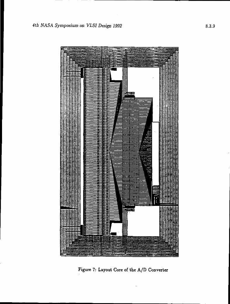
The final layout of the chip core is shown in Figure 7. On the left side of the chip is thecomparator chain and resistor ladder. A guard ring surrounds this section to isolate it fromthe digital side of the chip. The analog side is also fed from a power supply separated fromthe digital side, again to keep the sensitive analog circuitry as isolated as possible.
The dimensions of the core are 2,244 microns by 3,972 microns. The core was intention-ally left in this rectangular fashion for several reasons. First, to square up the chip wouldeither require several turns in the resistor ladder or running several critical signal lines oversusceptible circuitry. Both of these options are very undesirable because of the potentialerror terms that would be introduced. Additionally, since the long term purpose of this con-verter is to be used as a macrocell on a larger chip, there is really no need for the converterto be square. Therefore, it was decided to leave the core slightly rectangular.
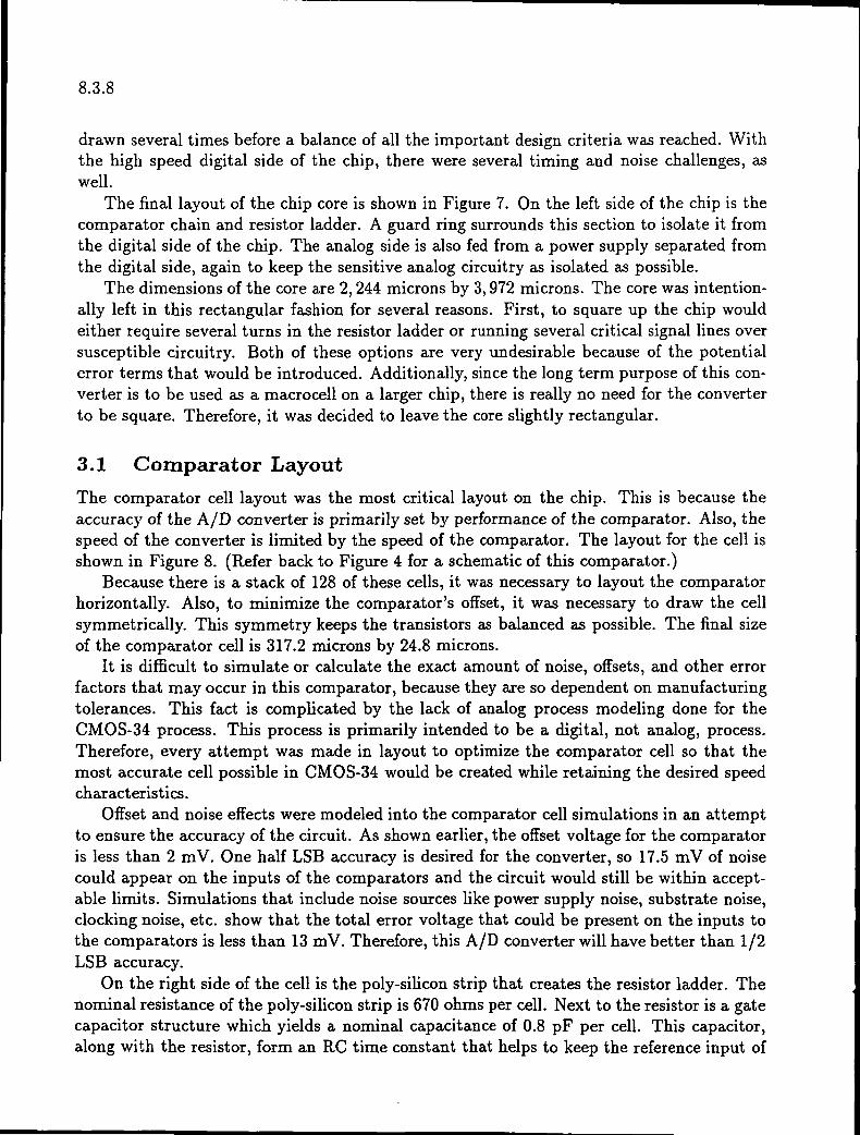
3.1 Comparator LayoutThe comparator cell layout was the most critical layout on the chip. This is because theaccuracy of the A/D converter is primarily set by performance of the comparator. Also, thespeed of the converter is limited by the speed of the comparator. The layout for the cell isshown in Figure 8. (Refer back to Figure 4 for a schematic of this comparator.)
Because there is a stack of 128 of these cells, it was necessary to layout the comparatorhorizontally. Also, to minimize the comparator's offset, it was necessary to draw the cellsymmetrically. This symmetry keeps the transistors as balanced as possible. The final sizeof the comparator cell is 317.2 microns by 24.8 microns.
It is difficult to simulate or calculate the exact amount of noise, offsets, and other errorfactors that may occur in this comparator, because they are so dependent on manufacturingtolerances. This fact is complicated by the lack of analog process modeling done for theCMOS-34 process. This process is primarily intended to be a digital, not analog, process.Therefore, every attempt was made in layout to optimize the comparator cell so that themost accurate cell possible in CMOS-34 would be created while retaining the desired speedcharacteristics.
Offset and noise effects were modeled into the comparator cell simulations in an attemptto ensure the accuracy of the circuit. As shown earlier, the offset voltage for the comparatoris less than 2 rnV. One half LSB accuracy is desired for the converter, so 17.5 mV of noisecould appear on the inputs of the comparators and the circuit would still be within accept-able limits. Simulations that include noise sources like power supply noise, substrate noise,clocking noise, etc. show that the total error voltage that could be present on the inputs tothe comparators is less than 13 mV. Therefore, this A/D converter will have better than 1/2LSB accuracy.
On the right side of the cell is the poly-silicon strip that creates the resistor ladder. Thenominal resistance of the poly-silicon strip is 670 ohms per cell. Next to the resistor is a gatecapacitor structure which yields a nominal capacitance of 0.8 pF per cell. This capacitor,along with the resistor, form an RC time constant that helps to keep the reference input of
4th NASA Symposium on VLSI Design 1992 8.3.9
Figure 7: Layout Core of the A/D Converter

8.3.10
Figure 8: Comparator Cell Layout
the comparator (Vref) noise free. This in turn helps to minimize the differential errors thatcould occur during the conversion process from reference node noise.
Many other enhancements to the layout have been made to keep the cell as accurate aspossible. First, the gates of large transistors are driven at both ends. This helps to minimizethe resistance of the gate poly-silicon along the length of the transistor. Next, the source anddrain diffusions of all the transistors are tied to metal down the entire length of the diffusion.This keeps source and drain resistance to a minimum, and thus increases the speed of thedevices. Thirdly, the power supply lines that run throughout the cell are sized such that thenoise on them (and thus the noise they couple into the cells) is kept to under 0.25 volts. Ifthe lines were sized too small, large voltage spikes would appear on them and potentiallycouple into the comparator circuitry. Additionally, the cell was drawn so that signal lines donot cross over any sensitive nodes in the comparator. In certain instances, signals crossingover certain nodes could capacitively couple enough charge onto the node to corrupt ordistort the comparator's operation. Also, the differential input pair of the comparator wassized minimally so that the noise that is coupled into the comparator through the parasiticcapacitors of the transistor pair would be small.
3.2 Digital Cells
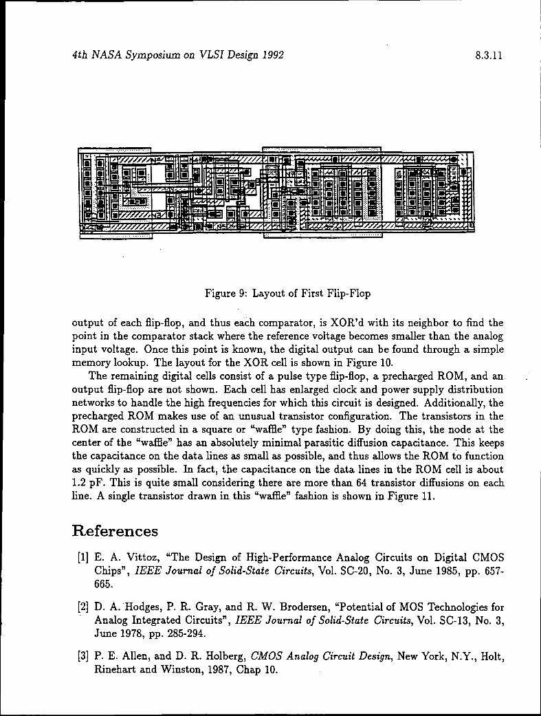
The stack of comparator cells feed directly into a stack of flip-flops. Recall that the com-parator uses half of the clock phase for pre-charge, and the other half to evaluate the currentanalog input. Because of this, the output of the comparator is only valid during half theclock. This flip-flop will take the output of the comparator, amplify it to full digital levels,and turn it into a signal that is stable for an entire clock. The layout for the cell is shownin Figure 9.
In addition to accepting an analog input, these flip-flops must be able to function withworst case parameters at 100 MHz. This is extremely fast for current CMOS technologies,but simulations show that these cells work at that speed. The flip-flop has a setup time ofless than 0.5 ns and a hold time of 0 ns. With these timings the flip-flop will accept 3.0 Vfor an input high voltage and 1.5 V for an input low voltage. It then drives the 0.6 pF ofcapacitance that the next cells (the exclusive or cells) presents to it in 3.0 ns.
The next stack of cells in the path of the data flow are the exclusive or (XOR) cells. The
4th NASA Symposium on VLSI Design 1992 8.3.11
Figure 9: Layout of First Flip-Flop
output of each flip-flop, and thus each comparator, is XOR'd with its neighbor to find thepoint in the comparator stack where the reference voltage becomes smaller than the analoginput voltage. Once this point is known, the digital output can be found through a simplememory lookup. The layout for the XOR cell is shown in Figure 10.
The remaining digital cells consist of a pulse type flip-flop, a precharged ROM, and anoutput flip-flop are not shown. Each cell has enlarged clock and power supply distributionnetworks to handle the high frequencies for which this circuit is designed. Additionally, theprecharged ROM makes use of an unusual transistor configuration. The transistors in theROM are constructed in a square or "waffle" type fashion. By doing this, the node at thecenter of the "waffle" has an absolutely minimal parasitic diffusion capacitance. This keepsthe capacitance on the data lines as small as possible, and thus allows the ROM to functionas quickly as possible. In fact, the capacitance on the data lines in the ROM cell is about1.2 pF. This is quite small considering there are more than 64 transistor diffusions on eachline. A single transistor drawn in this "waffle" fashion is shown in Figure 11.
References
[1] E. A. Vittoz, "The Design of High-Performance Analog Circuits on Digital CMOSChips", IEEE Journal of Solid-State Circuits, Vol. SC-20, No. 3, June 1985, pp. 657-665.
[2] D. A. Hodges, P. R. Gray, and R. W. Brodersen, "Potential of MOS Technologies forAnalog Integrated Circuits", IEEE Journal of Solid-State Circuits, Vol. SC-13, No. 3,June 1978, pp. 285-294.
[3] P. E. Allen, and D. R. Holberg, CMOS Analog Circuit Design, New York, N.Y., Holt,Rinehart and Winston, 1987, Chap 10.

8.3.12
Figure 10: Layout of XOR Cell
Drain
Polysilicon Gate
Diffusion
Figure 11: Waffle Type Transistor Configuration

8.3.13
[4] B. M. Gordon, "Linear Electronic Analog/Digital Conversion Architectures, Their Ori-gins, Parameters, Limitations, and Applications", IEEE Transactions on Circuits andSystems, Vol. CAS-25, No. 7, July 1978, pp. 391-418.
[5] A. Yukawa, "A CMOS 8-Bit High-Speed A/D Converter 1C" IEEE Journal of Solid-State Circuits, Vol. SC-20, No. 3, June 1985, pp. 775-779.
[6] T. Kumamoto, M. Nakaya, H. Honda, S. Asai, Y. Akasaka, and Y. Horiba, "An 8-bitHigh-Speed CMOS A/D Converter", IEEE Journal of Solid-State Circuits, Vol. SC-21,No. 6, Dec. 1986, pp. 976-982.
[7] A. G. F. Dingwall, "Monolithic Expandable 6 Bit 20 MHz CMOS/SOS A/D Converter",IEEE Journal of Solid-State Circuits, Vol. SC-14, No. 6, Dec. 1979, pp 926-932.
[8] D. A. Hodges "Analog Switches and Passive Elements in MOSLSI", Analog MOS Inte-grated Circuits, New York, N.Y., John Wiley and Sons, 1980, pp. 14-18.
[9] R. Gregorian, and G. C. Temes, Analog MOS Integrated Circuits For Signal Processing,. New York, N.Y., John Wiley and Sons, 1986, pp. 425-437.
[10] N. Weste, and K. Eshraghian, Principles of CMOS VLSI Design: A Systems Perspective,Reading, MA., 1985, Chap 4.