a comparative study on direct form -1, broadcast … comparative study on direct form... · a...
TRANSCRIPT
International Journal of Electronics, Communication & Soft Computing Science and Engineering
ISSN: 2277-9477, Volume 2, Issue 5
14
A Comparative Study on Direct form -1, Broadcast
and Fine grain structure of FIR digital filter Jaya Bar Madhumita Mukherjee
Abstract-This paper presents the VLSI architecture of pipeline
digital filter. The pipeline architecture is an efficient structure for
designing in real time embedded system. Our work concentrates on
designing digital filter using MATLAB FDA tool. Then we have
implemented this filter using 3 different pipeline structure, direct
form-1, broad cast and fine grain. We tested our algorithm using
Xilinx synthesis tool and then implemented on Spartan 3A family
XC3S700A-4fg484 FPGA device. The experimental results shows
that to design an area optimized filter we should use fine grain
pipeline structure, where as for high speed, we should use direct
form-1 structure of digital filter.
Keywords- FIR, FPGA, IIR, LTI, MATLAB, VLSI
I. INTRODUCTION Digital signal processing has a broad application in the field of
real time signal processing operation such as speech
processing, radar signal processing and different media
applications[1] .These computation intensive real time
application requires digital filter to perform the signal
processing operation. A digital filter is an important class of
linear time invariant system (LTI) that performs on a sample
discrete time signal to reduce or enhanced certain aspect of that
signal [2, 3]. In this paper we focus on designing low pass
pipeline FIR digital filter. The general form of digital filter
difference equation is given by organized as design of low pass
digital filter using equation 1.
(1)
Where Y(n) is the current filter outputs, the Y(n-k)’s are
current or previous filter inputs, the aK’s are the filter’s feed
forward co-efficient corresponding to the zeros of the filter, the
bK’s are the filter’s feedback co-efficient corresponding to the
pole of the filter, and N is the filter’s order[4,5]. Depending
upon the filter co-efficient there are two type of digital filter if
the co-efficient are fixed then it is frequency selective filter and
if the co-efficient updated at each iteration in order to minimize
the difference between the filter output and the desired signal
then it is a adaptive digital filter. The frequency selective filters
are of two type infinite impulse response (IIR) and finite
impulse response (FIR) digital filter [6].
We have designed the low pass FIR filter using MATLAB
FDA tool. Here we have developed different type of pipeline
digital filter structure such as direct form1, broadcast and fine
grain. For these structures we have tested our algorithm using
Xilinx ISE 13.4 synthesis tools and implemented in Spartan
3A. In our paper we have proposed pipelining technique for
designing the filter as in this method we can decompose the
sequential process into sub operations, with each sub process
being executed in a special dedicated segment. This technique
leads to reduction in critical path, power consumption and at
the same time it increases the clock frequency in comparison to
the parallel processing method of the designing the digital
filter. The rest of the paper is MATLAB FDA tool is shown in
section 2. The FPGA implementation of the direct form1
structure is given in section 3. The FPGA implementation of
the broad cast structure is shown in section 4. Section 5
contains the FPGA implementation of the fine grain structure.
The comparison of the optimized parameters of all designed
structure is given in section 6 and section 7 contains the
conclusion.
II. DESIGN OF FIR FILTER
For signal processing operation finite impulse response (FIR)
filter plays an important role, these are the digital filter that
computes the output response as the weighted, finite term-sum
of past, present and future values of the filter input [7] as given
in equation 2.
(2)
Where M1, M2 are finite. In this paper we will design a causal
FIR (finite impulse response) filter; the difference equation is
given as below in equation 3.
(3)
Where M is finite. To design this causal low pass filter, we
will use MATLAB FDA as the synthesis tool; the specification
is shown in the table 1. Depending upon the specification, we
will have the transfer function co-efficient as shown in the
table 2.
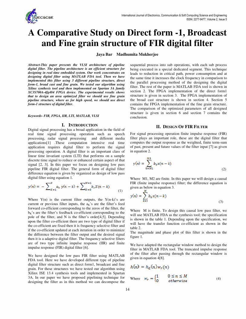
The magnitude and phase plot of this filter is shown in the
figure 1.
We have adapted the rectangular window method to design the
filter in MATLAB FDA tool. The truncated impulse response
of the filter after passing through the rectangular window is
given in equation 4[8].
Where (4)
International Journal of Electronics, Communication & Soft Computing Science and Engineering
ISSN: 2277-9477, Volume 2, Issue 5
15
and is the impulse response of the causal FIR filter.
In frequency domain, we can represent this truncated impulse
response is shown in the equation 5.
(5)
Properties Specification
response low pass
order
table yes
window rectangular window
cut-off frequency ( ) 0.25 (normalized)
attenuation at cut-off
frequency
6 db
Transfer function Co-efficient
h(0) 0.223
h(1) 0.278
h(2) 0.278
h(3) 0.223
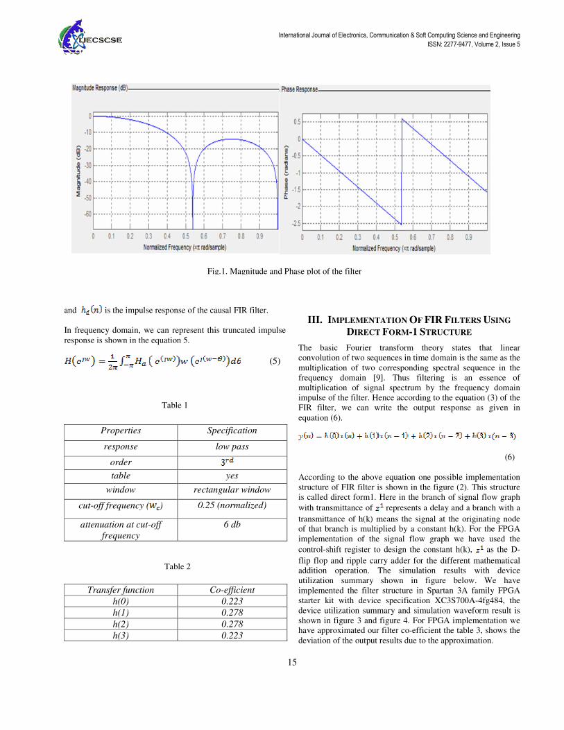
III. IMPLEMENTATION OF FIR FILTERS USING
DIRECT FORM-1 STRUCTURE
The basic Fourier transform theory states that linear
convolution of two sequences in time domain is the same as the
multiplication of two corresponding spectral sequence in the
frequency domain [9]. Thus filtering is an essence of
multiplication of signal spectrum by the frequency domain
impulse of the filter. Hence according to the equation (3) of the
FIR filter, we can write the output response as given in
equation (6).
(6)
According to the above equation one possible implementation
structure of FIR filter is shown in the figure (2). This structure
is called direct form1. Here in the branch of signal flow graph
with transmittance of represents a delay and a branch with a
transmittance of h(k) means the signal at the originating node
of that branch is multiplied by a constant h(k). For the FPGA
implementation of the signal flow graph we have used the
control-shift register to design the constant h(k), as the D-
flip flop and ripple carry adder for the different mathematical
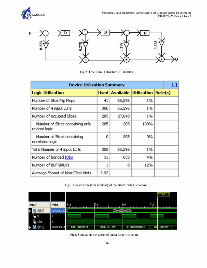
addition operation. The simulation results with device
utilization summary shown in figure below. We have
implemented the filter structure in Spartan 3A family FPGA
starter kit with device specification XC3S700A-4fg484, the
device utilization summary and simulation waveform result is
shown in figure 3 and figure 4. For FPGA implementation we
have approximated our filter co-efficient the table 3, shows the
deviation of the output results due to the approximation.
Table 1
Fig.1. Magnitude and Phase plot of the filter
Table 2
International Journal of Electronics, Communication & Soft Computing Science and Engineering
ISSN: 2277-9477, Volume 2, Issue 5
16
Fig.2.Direct form-1 structure of FIR filter
Fig.3. Device utilization summary of the direct form-1 structure
Fig4. Simulation waveform of direct form-1 structure
International Journal of Electronics, Communication & Soft Computing Science and Engineering
ISSN: 2277-9477, Volume 2, Issue 5
17
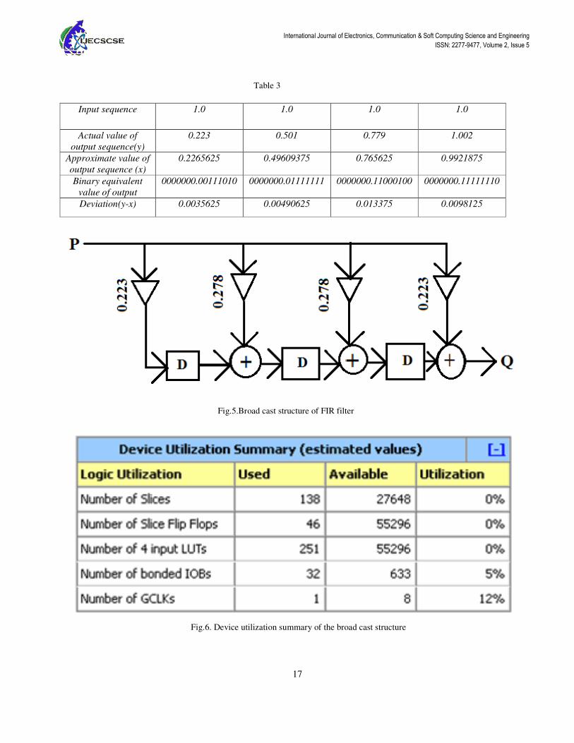
Input sequence 1.0 1.0 1.0 1.0
Actual value of
output sequence(y)
0.223 0.501 0.779 1.002
Approximate value of
output sequence (x)
0.2265625 0.49609375 0.765625 0.9921875
Binary equivalent
value of output
0000000.00111010 0000000.01111111 0000000.11000100 0000000.11111110
Deviation(y-x) 0.0035625 0.00490625 0.013375 0.0098125
Table 3
Fig.5.Broad cast structure of FIR filter
Fig.6. Device utilization summary of the broad cast structure
International Journal of Electronics, Communication & Soft Computing Science and Engineering
ISSN: 2277-9477, Volume 2, Issue 5
18
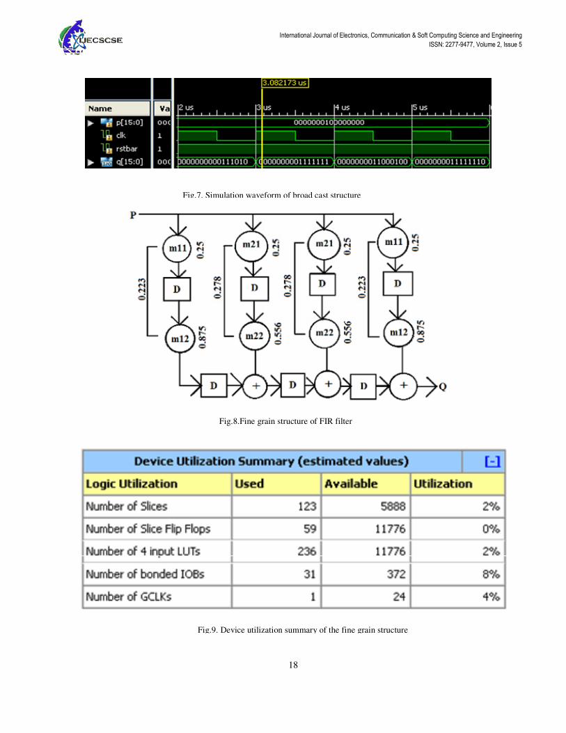
Fig.7. Simulation waveform of broad cast structure
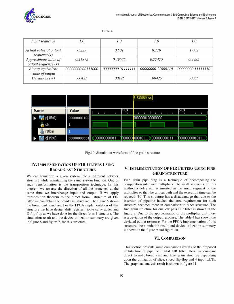
Fig.8.Fine grain structure of FIR filter
Fig.9. Device utilization summary of the fine grain structure
International Journal of Electronics, Communication & Soft Computing Science and Engineering
ISSN: 2277-9477, Volume 2, Issue 5
19
IV. IMPLEMENTATION OF FIR FILTERS USING
BROAD CAST STRUCTURE
We can transform a given system into a different network
structure while maintaining the same system function. One of
such transformation is the transposition technique. In this
theorem we reverse the direction of all the branches, at the
same time we interchange input and output. If we apply
transposition theorem to the direct form-1 structure of FIR
filter we can obtain the broad cast structure. The figure 5 shows
the broad cast structure. For the FPGA implementation of this
structure we have design shift register, ripple carry adder and
D-flip flop as we have done for the direct form-1 structure. The
simulation result and the device utilization summary are given
in figure 6 and figure 7, for this structure.
V. IMPLEMENTATION OF FIR FILTERS USING FINE
GRAIN STRUCTURE
Fine grain pipelining is a technique of decomposing the
computation intensive multipliers into small segments. In this
method a delay unit is inserted in the small segment of the
multiplier so that the critical path and the execution time can be
reduced [10].This structure has a disadvantage that due to the
insertion of pipeline latches the area requirement for such
structure becomes more in comparison to other structure. The
fine grain structure for our low pass FIR filter is shown in the
figure 8. Due to the approximation of the multiplier unit there
is a deviation of the output response. The table 4 has shown the
deviated output response. For the FPGA implementation of this
structure, the simulation result and device utilization summary
is shown in the figure 9 and figure 10.
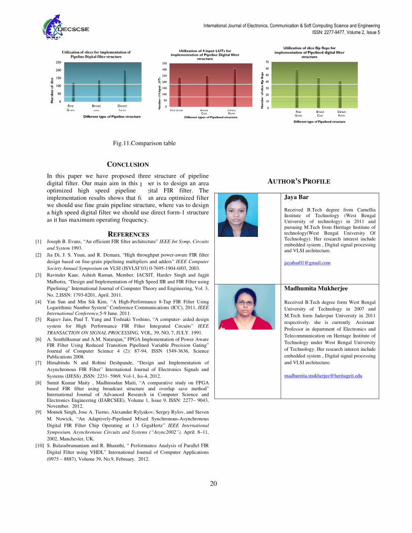
VI. COMPARISON
This section presents some comparison results of the proposed
architecture of pipeline digital FIR filter. Here we compare
direct form-1, broad cast and fine grain structure depending
upon the utilization of slice, sliced flip-flop and 4 input LUTs.
The graphical analysis result is shown in figure 11.
Table 4
Input sequence 1.0 1.0 1.0 1.0
Actual value of output
sequence(y)
0.223 0.501 0.779 1.002
Approximate value of
output sequence (x)
0.21875 0.49675 0.77475 0.9935
Binary equivalent
value of output
00000000.00111000 00000000.01111111 00000000.11000110 00000000.11111110
Deviation(y-x) .00425 .00425 .00425 .0085
Fig.10. Simulation waveform of fine grain structure
International Journal of Electronics, Communication & Soft Computing Science and Engineering
ISSN: 2277-9477, Volume 2, Issue 5
20
CONCLUSION
In this paper we have proposed three structure of pipeline
digital filter. Our main aim in this paper is to design an area
optimized high speed pipeline digital FIR filter. The
implementation results shows that for an area optimized filter
we should use fine grain pipeline structure, where vas to design
a high speed digital filter we should use direct form-1 structure
as it has maximum operating frequency.
REFERENCES
[1] Joseph B. Evans, “An efficient FIR filter architecture” IEEE Int Symp, Circuits
and System 1993.
[2] Jia Di, J. S. Yuan, and R. Demara, “High throughput power-aware FIR filter
design based on fine-grain pipelining multipliers and adders” IEEE Computer
Society Annual Symposium on VLSI (ISVLSI’03) 0-7695-1904-0/03, 2003.
[3] Ravinder Kaur, Ashish Raman, Member, IACSIT, Hardev Singh and Jagjit
Malhotra, “Design and Implementation of High Speed IIR and FIR Filter using
Pipelining” International Journal of Computer Theory and Engineering, Vol. 3,
No. 2,ISSN: 1793-8201, April. 2011.
[4] Yan Sun and Min Sik Kim, “A High-Performance 8-Tap FIR Filter Using
Logarithmic Number System” Conference Communications (ICC), 2011, IEEE
International Conference,5-9 June. 2011.
[5] Rajeev Jain, Paul T. Yang and Toshiaki Yoshino, “A computer- aided design
system for High Performance FIR Filter Integrated Circuits” IEEE
TRANSACTION ON SIGNAL PROCESSING, VOL, 39, NO, 7, JULY. 1991.
[6] A. Senthilkumar and A.M. Natarajan,” FPGA Implementation of Power Aware
FIR Filter Using Reduced Transition Pipelined Variable Precision Gating”
Journal of Computer Science 4 (2): 87-94, ISSN 1549-3636, Science
Publications 2008.
[7] Himabindu N and Rohini Deshpande, “Design and Implementation of
Asynchronous FIR Filter” International Journal of Electronics Signals and
Systems (IJESS) ,ISSN: 2231- 5969, Vol-1, Iss-4, 2012.
[8] Sumit Kumar Maity , Madhusudan Maiti, “A comparative study on FPGA
based FIR filter using broadcast structure and overlap save method”
International Journal of Advanced Research in Computer Science and
Electronics Engineering (IJARCSEE), Volume 1, Issue 9, ISSN: 2277– 9043,
November. 2012.
[9] Montek Singh, Jose A. Tierno, Alexander Rylyakov, Sergey Rylov, and Steven
M. Nowick, “An Adaptively-Pipelined Mixed Synchronous-Asynchronous
Digital FIR Filter Chip Operating at 1.3 GigaHertz” IEEE International
Symposium, Asynchronous Circuits and Systems (“Async2002”), April. 8–11,
2002, Manchester, UK.
[10] S. Balasubramaniam and R. Bharathi, “ Performance Analysis of Parallel FIR
Digital Filter using VHDL” International Journal of Computer Applications
(0975 – 8887), Volume 39, No.9, February. 2012.
AUTHOR’S PROFILE
Jaya Bar
Received B.Tech degree from Camellia Institute of Technology (West Bengal
University of technology) in 2011 and
pursuing M.Tech from Heritage Institute of
technology(West Bengal University Of
Technology). Her research interest include
embedded system , Digital signal processing
and VLSI architecture.
Madhumita Mukherjee
Received B.Tech degree form West Bengal
University of Technology in 2007 and
M.Tech form Jadavpur University in 2011
respectively. she is currently Assistant
Professor in department of Electronics and
Telecommunication on Heritage Institute of
Technology under West Bengal University
of Technology. Her research interest include
embedded system , Digital signal processing
and VLSI architecture.
Fig.11.Comparison table