1 radiation hardness of monolithic active pixel sensors dennis doering, goethe-university frankfurt...
TRANSCRIPT
1
Radiation Hardness of Monolithic Active Pixel Sensors
Dennis Doering, Goethe-University Frankfurt am Main
on behalf of the CBM-MVD-Collaboration
Outline- Operation principle of MAPS - Radiation damage effects- MAPS with high-resistivity epitaxial layer - Parameters of radiation hardness- Conclusion
/172/21
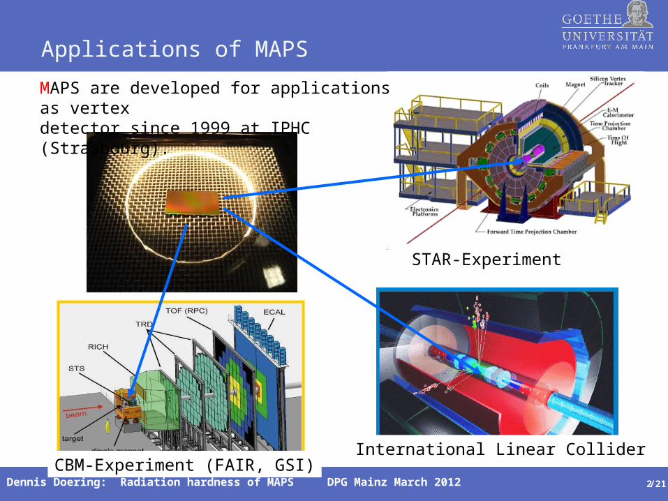
Applications of MAPS
Dennis Doering: Radiation hardness of MAPS DPG Mainz March 2012
Picture STAR
Picture CBM
International Linear ColliderCBM-Experiment (FAIR, GSI)
STAR-Experiment
MAPS are developed for applications as vertex detector since 1999 at IPHC (Strasbourg).
/17/21
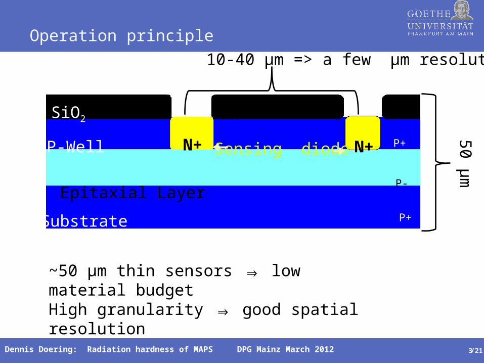
Operation principle
Dennis Doering: Radiation hardness of MAPS DPG Mainz March 2012 3
SiO2
N+ P+
P-
P+
Sensing diode
Epitaxial Layer
P-Well
Substrate
N+
50 µm
~50 µm thin sensors low material budget ⇒High granularity good spatial resolution ⇒
10-40 µm => a few µm resolution
/17/21
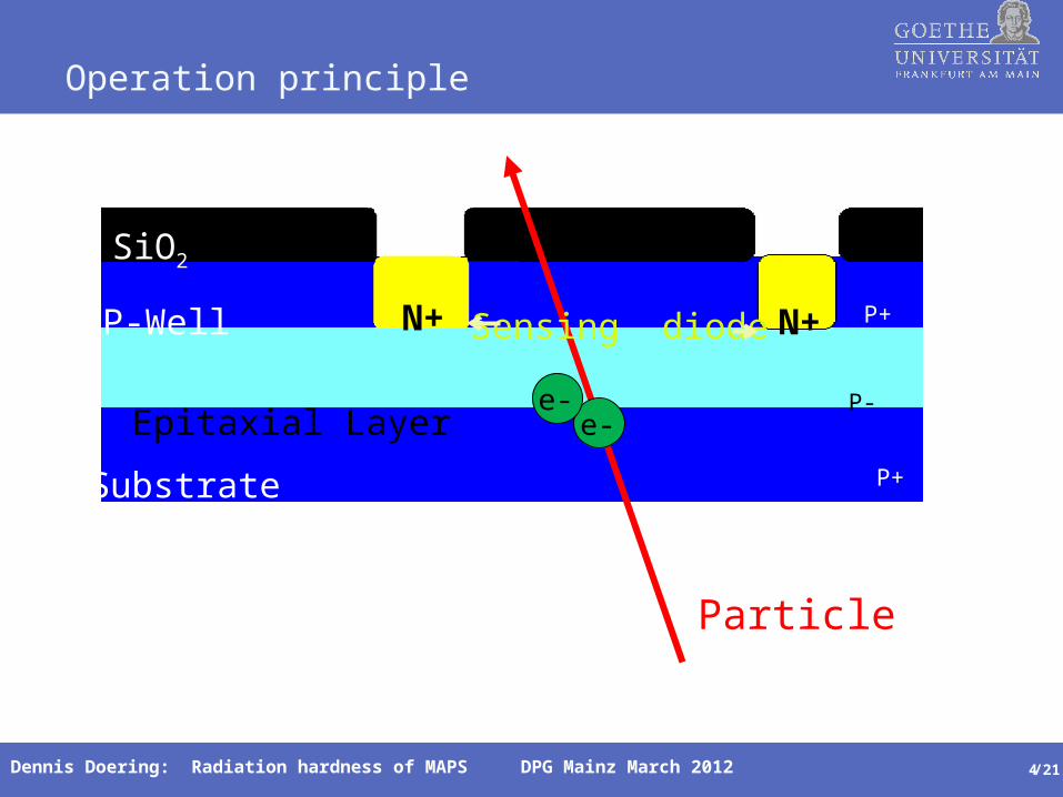
Operation principle
Dennis Doering: Radiation hardness of MAPS DPG Mainz March 2012 4
SiO2
N+ P+
P-
P+
Epitaxial Layer
P-Well
Substrate
e-
N+
e-
Particle
Sensing diode
/17/21
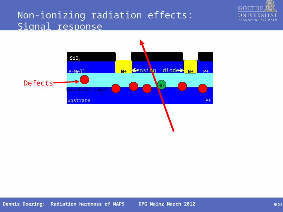
Non-ionizing radiation effects:Signal response
Dennis Doering: Radiation hardness of MAPS DPG Mainz March 2012 5
SiO2
N+ P+
P-
P+
Epitaxial Layer
P-Well
Substrate
N+
e-
Sensing diode
Defects
/17/21
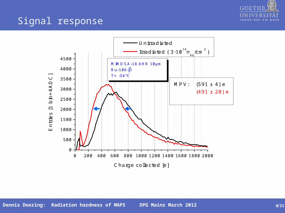
Signal response
Dennis Doering: Radiation hardness of MAPS DPG Mainz March 2012 6
0 200 400 600 800 1000 1200 1400 1600 1800 20000
500
1000
1500
2000
2500
3000
3500
4000
4500
En
trie
s [1
bin
=4
AD
C]
Charge collected [e]
Unirradiated
Irradiated ( 3·1014neq
/cm2 )
MIMOSA-18 AHR 10µm Ru-106-T= -34°C
MPV: (591 ± 4) e(491 ± 20) e
/17/21
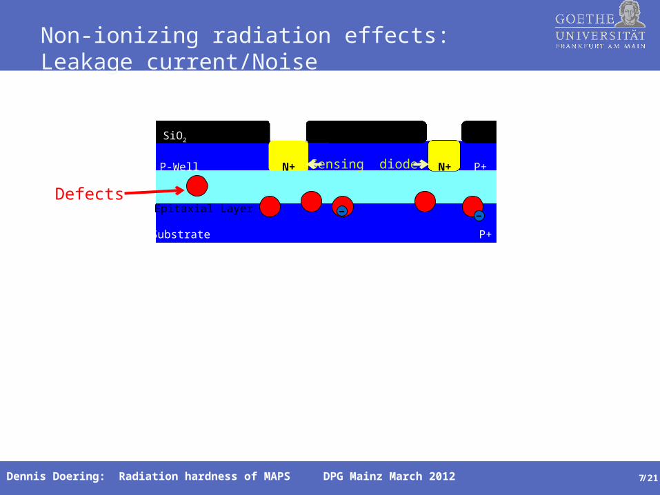
Non-ionizing radiation effects: Leakage current/Noise
Dennis Doering: Radiation hardness of MAPS DPG Mainz March 2012 7
SiO2
N+ P+
P-
P+
Epitaxial Layer
P-Well
Substrate
N+
--
Sensing diode
Defects
/17/21
5
10
15
20
25
30
35
40
45
50
55
60
No
ise
[e]
Temperature [°C]
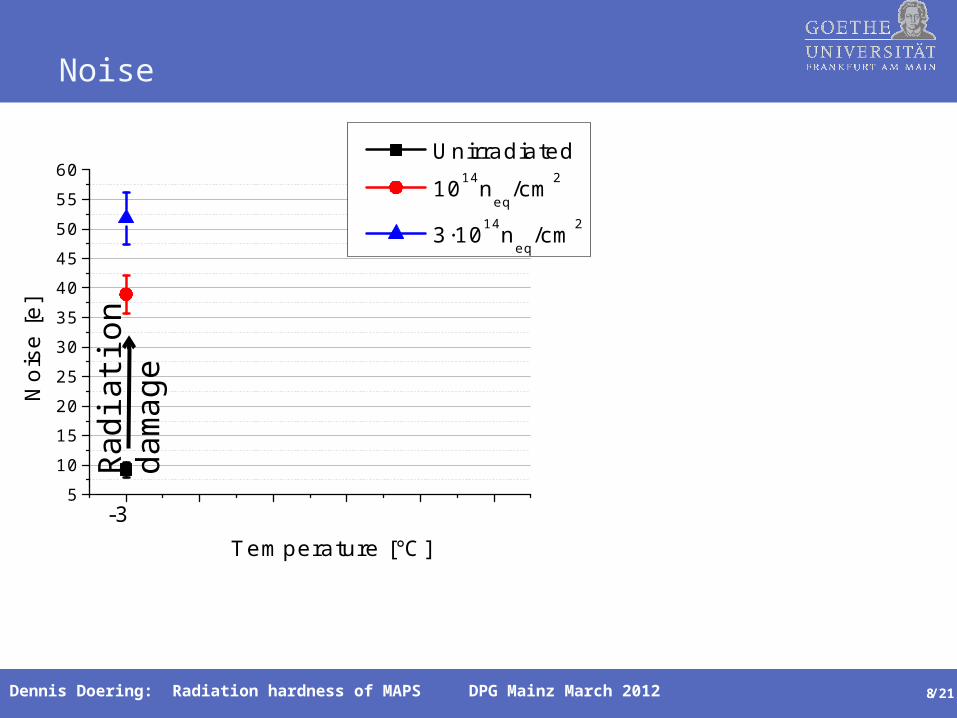
Unirradiated
1014neq
/cm2
3·1014neq
/cm2
-3
Noise
Dennis Doering: Radiation hardness of MAPS DPG Mainz March 2012 8
Rad
iatio
nda
mag
e
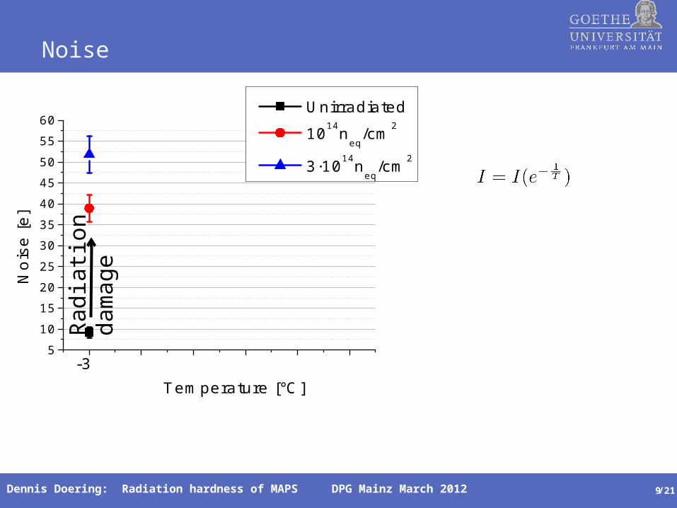
/17/21
5
10
15
20
25
30
35
40
45
50
55
60
No
ise
[e]
Temperature [°C]
Unirradiated
1014neq
/cm2
3·1014neq
/cm2
-3
Noise
Dennis Doering: Radiation hardness of MAPS DPG Mainz March 2012 9
Rad
iatio
nda
mag
e
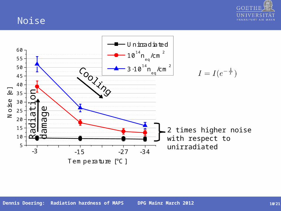
/17/21
5
10
15
20
25
30
35
40
45
50
55
60
-34-27-15
No
ise
[e]
Temperature [°C]
Unirradiated
1014neq
/cm2
3·1014neq
/cm2
-3
Noise
Dennis Doering: Radiation hardness of MAPS DPG Mainz March 2012 10
Rad
iatio
nda
mag
e
Cooling
2 times higher noise with respect to unirradiated
/17/21
Non-ionizing radiation effects
Dennis Doering: Radiation hardness of MAPS DPG Mainz March 2012 11
SiO2
N+ P+
P-
P+
Epitaxial Layer
P-Well
Substrate
N+
e-
--
Sensing diode
Defects
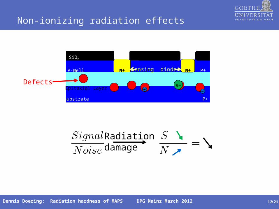
/17/21
Non-ionizing radiation effects
Dennis Doering: Radiation hardness of MAPS DPG Mainz March 2012 12
SiO2
N+ P+
P-
P+
Epitaxial Layer
P-Well
Substrate
N+
e-
--
Radiationdamage
Sensing diode
Defects
/17/21
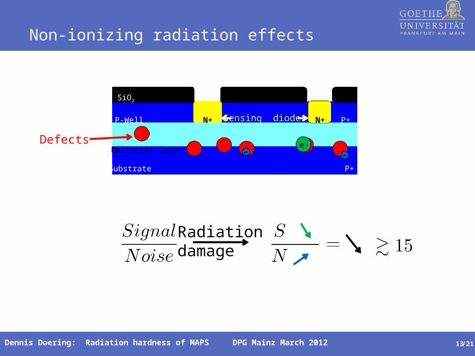
Non-ionizing radiation effects
Dennis Doering: Radiation hardness of MAPS DPG Mainz March 2012 13
SiO2
N+ P+
P-
P+
Epitaxial Layer
P-Well
Substrate
N+
e-
--
Radiationdamage
Sensing diode
Defects
/17/21
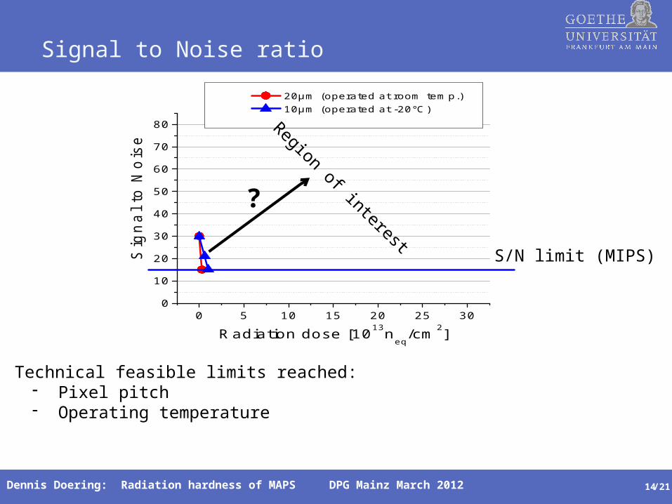
Signal to Noise ratio
Dennis Doering: Radiation hardness of MAPS DPG Mainz March 2012 14
0 5 10 15 20 25 300
10
20
30
40
50
60
70
80
20µm (operated at room temp.) 10µm (operated at -20°C)
Sig
na
l to
No
ise
Radiation dose [1013neq
/cm2]
S/N limit (MIPS)
Technical feasible limits reached:- Pixel pitch- Operating temperature
Region of interest
?
/17/21
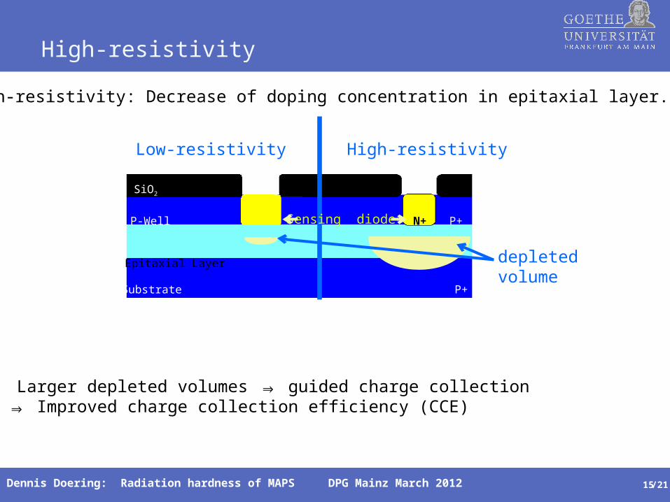
High-resistivity
Dennis Doering: Radiation hardness of MAPS DPG Mainz March 2012 15
Larger depleted volumes guided charge collection ⇒ ⇒ Improved charge collection efficiency (CCE)
SiO2
N+ P+
P-
P+
Epitaxial Layer
P-Well
Substrate
depleted volume
Low-resistivity High-resistivity
High-resistivity: Decrease of doping concentration in epitaxial layer.
Sensing diode
/17/21
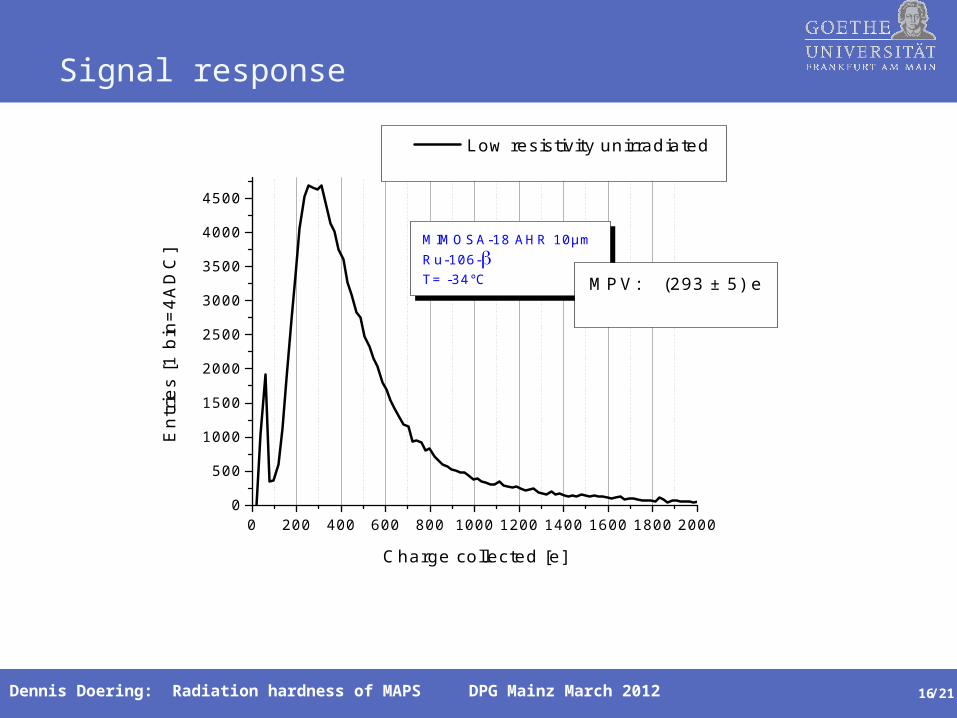
Signal response
Dennis Doering: Radiation hardness of MAPS DPG Mainz March 2012 16
0 200 400 600 800 1000 1200 1400 1600 1800 20000
500
1000
1500
2000
2500
3000
3500
4000
4500
En
trie
s [1
bin
=4
AD
C]
Charge collected [e]
Low resistivity unirradiated
MIMOSA-18 AHR 10µm Ru-106-T= -34°C MPV: (293 ± 5) e
/17/21
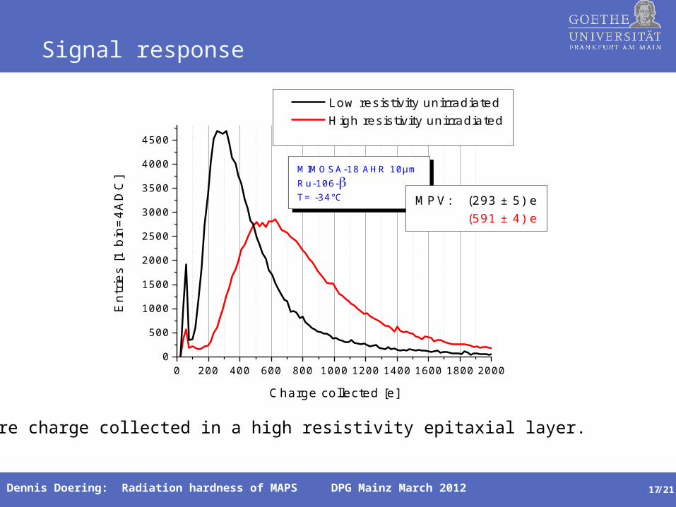
Signal response
Dennis Doering: Radiation hardness of MAPS DPG Mainz March 2012 17
More charge collected in a high resistivity epitaxial layer.
0 200 400 600 800 1000 1200 1400 1600 1800 20000
500
1000
1500
2000
2500
3000
3500
4000
4500
En
trie
s [1
bin
=4
AD
C]
Charge collected [e]
Low resistivity unirradiated High resistivity unirradiated
MIMOSA-18 AHR 10µm Ru-106-T= -34°C MPV: (293 ± 5) e
(591 ± 4) e
/17/21
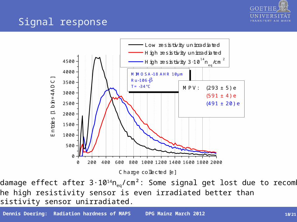
Signal response
Dennis Doering: Radiation hardness of MAPS DPG Mainz March 2012 18
Radiation damage effect after 3·1014neq/cm²: Some signal get lost due to recombinations. However, the high resistivity sensor is even irradiated better than the low resistivity sensor unirradiated.
0 200 400 600 800 1000 1200 1400 1600 1800 20000
500
1000
1500
2000
2500
3000
3500
4000
4500
En
trie
s [1
bin
=4
AD
C]
Charge collected [e]
Low resistivity unirradiated High resistivity unirradiated
High resistivity 3·1014neq
/cm2
MIMOSA-18 AHR 10µm Ru-106-T= -34°C MPV: (293 ± 5) e
(591 ± 4) e(491 ± 20) e
/17/21
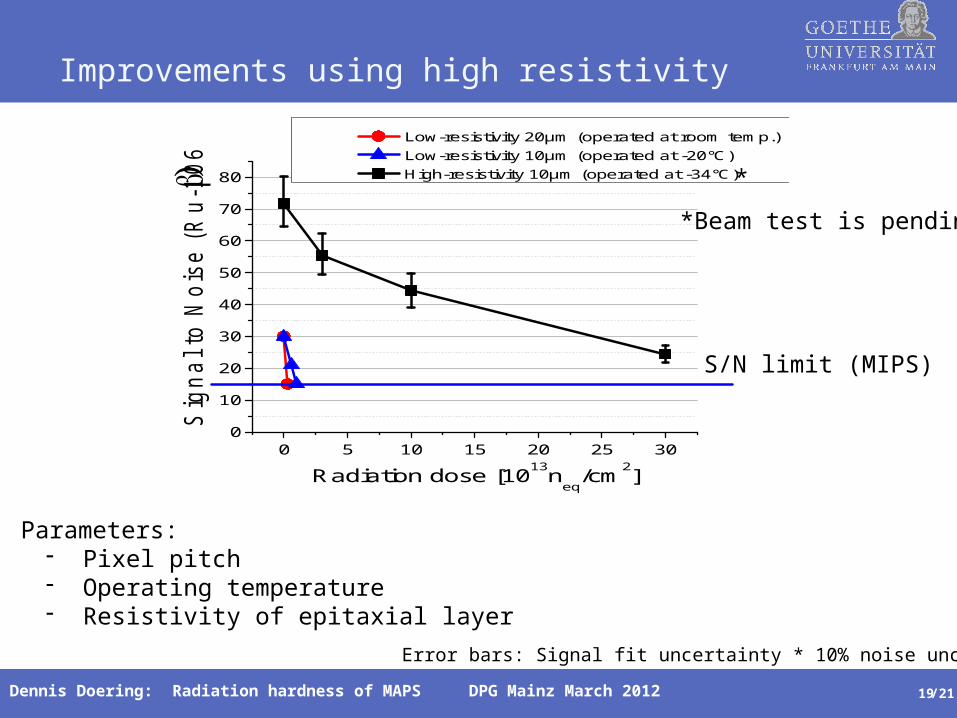
Improvements using high resistivity
Dennis Doering: Radiation hardness of MAPS DPG Mainz March 2012 19
0 5 10 15 20 25 300
10
20
30
40
50
60
70
80
Low-resistivity 20µm (operated at room temp.) Low-resistivity 10µm (operated at -20°C) High-resistivity 10µm (operated at -34°C)
Sig
nal to
Nois
e (R
u-1
06
)
Radiation dose [1013neq
/cm2]
Error bars: Signal fit uncertainty * 10% noise uncertainty
*Beam test is pending
S/N limit (MIPS)
*
Parameters:- Pixel pitch- Operating temperature- Resistivity of epitaxial layer
/17/21
How to improve the non-ionizing radiation hardness of MAPS:- Operate the sensor at low temperature ( -30°C)- Small pixel pitch ( 10µm)- High-resistivity epitaxial layer (used here 400 Ωcm)
Conclusion
Dennis Doering: Radiation hardness of MAPS DPG Mainz March 2012 20
/17/21
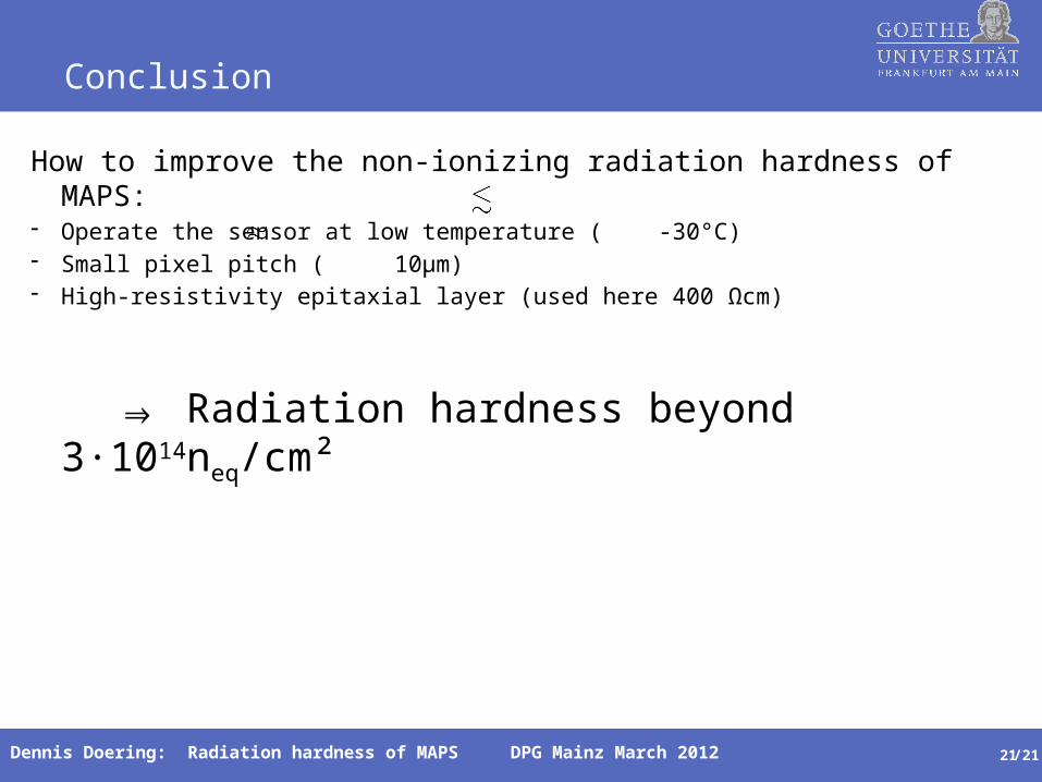
How to improve the non-ionizing radiation hardness of MAPS:- Operate the sensor at low temperature ( -30°C)- Small pixel pitch ( 10µm)- High-resistivity epitaxial layer (used here 400 Ωcm)
⇒ Radiation hardness beyond 3·1014neq/cm²
Conclusion
Dennis Doering: Radiation hardness of MAPS DPG Mainz March 2012 21