wsm-ble241 dk 801107 rev c user guide
TRANSCRIPT

MBN52832DK User Guide
Page 1 of 18
Copyright© Murata Manufacturing Co., Ltd. All Rights Reserved. Aug 2017 www.murata.com
Version: 1.0 Release Date: August 18, 2017
Murata reserves the right to make changes in specifications at anytime and without notice. The information furnished
in this user guide is believed to be accurate and reliable. However, no responsibility is assumed by Murata for its use,
nor any infringements of patents or other rights of third parties resulting from its use. No license is generated under
any rights of Murata or its supporters unless specifically agreed.
WSM-BLE241 DK 801107 Rev C
User Guide

MBN52832DK User Guide
Page 2 of 18
Release Record
Version Number Release Date Comments Version 0.1 10/27/2016 Initial draft for 801107 Rev A Version 0.2 2/17/2017 Updated for 801107 Rev B Version 0.3 7/7/2017 Updated for 801107 Rev C Version 1.0 8/18/2017 Clarified setup for battery powered case

MBN52832DK User Guide
Page 3 of 18
THE TABLE OF CONTENTS
1. INTRODUCTION ................................................................................................................................. 6
1.1 ACRONYMS .......................................................................................................................................... 6 1.2 REFERENCES ........................................................................................................................................ 6
2. SETTING UP THE MBN52832DK FOR WINDOWS....................................................................... 7
2.1 INTERFACE MODULE (IM) .................................................................................................................... 7 2.1.1 EVB power supply selection ....................................................................................................... 8 2.1.2 Application buttons...................................................................................................................... 9 2.1.3 IM-BM interface header pads ...................................................................................................... 9 2.1.4 Programming and debug interface ............................................................................................... 9 2.1.5 UART interface ......................................................................................................................... 10 2.1.6 Power consumption measurement ............................................................................................. 10
2.2 BREAKAWAY MODULE (BM) ............................................................................................................. 11 2.2.1 32KHz clock .............................................................................................................................. 11 2.2.2 2.4GHz antenna configuration ................................................................................................... 11 2.2.3 NFC antenna .............................................................................................................................. 12 2.2.4 Application LEDs ...................................................................................................................... 12 2.2.5 Module IO header pads .............................................................................................................. 13
2.3 CONNECT AND TEST THE MBN52832DK ........................................................................................... 13 2.4 APPLICATION DEVELOPMENT ............................................................................................................. 15
2.4.1 MBN52832DK compatibility with nRF52 SDK ....................................................................... 15 2.4.2 Connect the MBN52832DK Evaluation Board ......................................................................... 16 2.4.3 Verifying USB Driver Installations ........................................................................................... 16
3. EVB SCHEMATIC ............................................................................................................................. 17

MBN52832DK User Guide
Page 4 of 18
TABLE of figures
Figure 1 MBN52832 Evaluation Board Revision C ........................................................................................ 6 Figure 2 MBN52832 Development Kit Evaluation Board .............................................................................. 7 Figure 3 Interface Module (IM) ....................................................................................................................... 7 Figure 4 Location of resisters connecting IM to module ................................................................................. 9 Figure 5 Breakaway Module (BM)................................................................................................................ 11 Figure 6 R45 and R46 on the BM .................................................................................................................. 11 Figure 7 2.4GHz antenna selection ................................................................................................................ 12 Figure 8 R37 and R38 on the BM .................................................................................................................. 12 Figure 9 R29 and R31 on the BM .................................................................................................................. 12 Figure 10 Sample nRF52 DK webpage ......................................................................................................... 14 Figure 11 nRFgo Studio ................................................................................................................................ 14 Figure 12 Configuration for application development with nRF52 SDK ...................................................... 15 Figure 13 Screenshot showing installed J-Link drivers ................................................................................. 16

MBN52832DK User Guide
Page 5 of 18
TABLE OF TABLES
Table 1 EVB power supply selection .............................................................................................................. 8 Table 2 IM-module IO interface ...................................................................................................................... 9 Table 3 UART interface ................................................................................................................................ 10 Table 4 BM module IO pads ......................................................................................................................... 13 Table 5 MBN52832DK and nRF52 DK signal map ...................................................................................... 16

MBN52832DK User Guide
Page 6 of 18
1. Introduction The MBN52832Development Kit (MBN52832DK) is an evaluation and application development kit for MBN52832 BLE Module (ordering part number WSM-BL241-ADA-008), a compact Bluetooth Smart module which combines a 2.4 GHz transceiver, an ARM Cortex-M4 CPU, flash memory, a high speed clock and an on-board antenna in a small package. MBN52832DK can serve as a software development platform for creating Bluetooth Smart and NFC-enabled systems using the Nordic nRF52 SDK [1]. This document provides the information for setting up the MBN52832DK with hardware version 801107 Rev C. Please ensure that the revision is correct prior to using this document, as shown below.
Ensure it’s Rev C
Figure 1 MBN52832 Evaluation Board Revision C
1.1 Acronyms
Acronym Meaning
API Application Programming Interface BLE Bluetooth Low Energy EVB Evaluation Board MBN52832DK MBN52832 Development Kit FW Firmware GPIO General Purpose Input/Output NFC Near Field Communication PC Personal Computer SW Software SWD Serial Wire Debug UART Universal Asynchronous Receiver/Transmitter USB Universal Serial Bus
1.2 References [1] Nordic nRF52 Series SoC (http://www.nordicsemi.com/eng/Products/nRF52-Series-SoC)

MBN52832DK User Guide
Page 7 of 18
2. Setting up the MBN52832DK for Windows The MBN52832Development Kit (MBN52832DK) supports the evaluation and development of smart IoT wireless networking products using BLE and NFC. It consists of an evaluation board (EVB), a quick start guide and this user guide. The EVB consists of two parts, the Interface Module (IM) and the Breakaway Module (BM), as shown in Figure 2. IM provides a dual USB-SWD and USB-UART interface to support firmware download and application software debugging and development; BM contains a MBN52832 module preconfigured with an onboard 2.4GHz antenna, LEDs, 32 KHz sleep clock and a NFC antenna. There is also an u.FL connector for RF evaluation. The BM can be separated from the IM and used as a standalone carrier board of MBN52832for product prototyping.
Breakaway Module (BM)Interface Module (IM)
Figure 2 MBN52832 Development Kit Evaluation Board
The MBN52832DK is discussed in detail in the ensuing sections.
2.1 Interface Module (IM) IM provides the USB-SWD and USB-UART interfaces for application development. Some major components of the Interface Module are shown in Figure 3.
Micro-USB connector
J4, J5, J6
Battery holder
SW1, SW2
JP4
Figure 3 Interface Module (IM)

MBN52832DK User Guide
Page 8 of 18
Micro-USB connector supporting USB-SWD and USB-UART interfaces through the Atmel processor
Coin-cell battery holder
Application buttons (SW1, SW2)
Pads (J4) to select power supply source between VUSB and VEXT
Pads (J5) to measure power consumption by the BM
Pads (J6) for extern 5V power supply (VEXT)
Pads (JP4) to access select I/O pins of the BM
2.1.1 EVB power supply selection
The EVB power can be provided by a USB host, an external 5V supply or a coin cell battery. By default, USB is selected as the power source for the EVB; R17 is installed. Using a different supply requires the modifications listed in Table 1.
R49
J4
R17
R22
R18
J6
EVB power source Remark
USB By default, R17 is installed, both R18 and R22 are not installed and the USB source is selected.
Install the 0Ω resister R17 or short J4 if that is installed
Ensure that either R22 is removed or a coin cell battery is not installed
Connect micro-USB interface to host
External 5V DC The following modifications are required:
Remove R17
Open J4 if that is installed
Ensure that either R22 is removed or a coin cell battery is not installed
Connect GND and VCC_EXT (J6) to external 5V supply
CR2032 battery The following configuration modifications are needed:
Remove R18 if that is installed.
Remove R49. Reinstall R49 for FW download/JTAG debugging.
Insert a fresh CR2032 battery in the battery holder.
Table 1 EVB power supply selection

MBN52832DK User Guide
Page 9 of 18
2.1.2 Application buttons
The two buttons (SW1 and SW2) on the IM are connected to MBN52832 on the BM. The buttons SW1 and SW2, respectively, are connected to P0.13 and P0.14 on the module.
2.1.3 IM-BM interface header pads
IM provides header pads (JP4) for select module I/Os. Depending on the application needs, the resisters listed below may be removed to disconnect the associated module pins from the IM board so those pins may be controlled by the nRF52 firmware. P0.13 and P0.14 are connected to switches on the IM, so they may be used by the application without further modification if the switches are not pressed.
R39
R41
R40
R42
R49
R48
R50
R51
Figure 4 Location of resisters connecting IM to module
Connection MBN52832 pins
R39 P0.05
R40 P0.06
R41 P0.07
R42 P0.08
SW1 P0.13
SW2 P0.14
R48 P0.18
R49 P0.21
R50 SWDIO
R51 SWDCLK
Table 2 IM-module IO interface
2.1.4 Programming and debug interface
The EVB provides a mechanism for programming and debugging applications on the MBN52832 module using tools such as nRFgo studio and J-Link through the USB-SWD interface as detailed in Section 2.4.

MBN52832DK User Guide
Page 10 of 18
2.1.5 UART interface
The EVB also provides a serial interface to the MBN52832 module through the USB-UART interface. Resisters R39 – R42 may be removed to disconnect the USB-UART interface. The signal connections are listed below.
R41
R40
R42
R39
Resistor MBN52832 pins MBN52832
Signal
Remark
R39 P0.05 RTS/ Connect to host CTS/
R40 P0.06 TXD Connect to host RXD
R41 P0.07 CTS/ Connect to host RTS/
R42 P0.08 RXD Connect to host TXD
Table 3 UART interface
2.1.6 Power consumption measurement
The power consumed by the out-of-box configured Breakaway Module (BM) can be measured by one of the following methods:
1. Remove all the resistors shown in Figure 4 (details in Table 2) to isolate the BM and then apply a 3.3V power meter at VCC_nRF (J5.2) and note the power consumed. IM is not powered.
2. Remove R19 and all the resistors shown in Figure 4 (details in Table 2) to isolate the BM and then measure the current across J5. IM is powered by any of the 3 power sources.
R19
J5
3. Breaking off the BM and measure current applied to VCC_nRF.

MBN52832DK User Guide
Page 11 of 18
2.2 Breakaway Module (BM) The Breakaway Module (BM) contains a MBN52832 module preconfigured with an onboard 2.4GHz antenna, two LEDs, 32 KHz sleep clock and a NFC antenna. There is also an u.FL connector for RF evaluation and header pads to access the I/O pins of the module. BM can be separated from the IM and used as a standalone carrier board of MBN52832 for product prototyping.
WSM-BL241 module
with onboard antenna
NFC antenna
UFL connector
LEDs
IO pads
Figure 5 Breakaway Module (BM)
Some major components of the BM are shown in Figure 5.
MBN52832 module supporting Nordic nRF52 SDK
2.4GHz antenna for BLE application
NFC antenna for NFC tag
2 LEDs
u.FL connector for RF testing
Pads for accessing MBN52832 IO pins
2.2.1 32KHz clock
The 32KHz clock is connected to P0.00 and P0.01 on the module. If this clock is not needed, then resisters R43 and R44 may be installed and R45 and R46 removed to free these pins for application usage.
R45
R46
R43
R44
Figure 6 R45 and R46 on the BM
2.2.2 2.4GHz antenna configuration
The out-of-box configuration of the MBN52832DK uses the onboard 2.4GHz antenna for the application; there is also an u.FL connector for RF evaluation. Antenna selection is based on the configurations shown below.

MBN52832DK User Guide
Page 12 of 18
Selection R20 R47 L3 Description
Onboard antenna open 1.0 pF 1.1 nH Default configuration
u.FL connector 0Ω open open RF testing usage
Onboard antenna
UFL connector
R20
R47 and L3
Figure 7 2.4GHz antenna selection
2.2.3 NFC antenna
The NFC antenna is connected to P0.09 and P0.10 on the module. If NFC is not used, then resisters R37 and R38 may be removed to free these pins for application usage.
R38
R37
Figure 8 R37 and R38 on the BM
2.2.4 Application LEDs
BM has 2 LEDs. LED1 and LED2, respectively, are connected to P0.17 and P0.18 on the module. An LED is turned on by driving the respective IO pin low (0). Resisters R29 and R31, respectively, may be removed to disconnect LED1 and LED2 from the module IO pins.
R31
R29
LED2
LED1
Figure 9 R29 and R31 on the BM

MBN52832DK User Guide
Page 13 of 18
2.2.5 Module IO header pads
The BM provides header pads (JP2 and JP3) for select module I/Os. The resisters listed below may be removed to free the associated module pins so they may be controlled by the nRF52 firmware. In the default configuration where the BM board is attached to the IM board, additional resisters on the IM board may also need to be removed (Section 2.1.3).
MBN52832 pins BM pad BM resister IM Connection
VCC JP2: VCC_nRF VCC_nRF
GND JP2: GND GND
P0.00 M_SCLK2/P0.00 R45, R44
P0.01 M_SCLK1/P0.01 R46, R43
P0.02 JP3: P0.02
P0.03 JP3: P0.03
P0.04 JP3: P0.04
P0.05 JP2: P0.05/RTS R39
P0.06 JP2: P0.06/TX R40
P0.07 JP2: P0.07/CTS R41
P0.08 JP2: P0.08/RX R42
P0.09 NFC1/P0.09 R37
P0.10 NFC2/P0.10 R38
P0.13 JP2: P0.13 SW1
P0.14 JP2: P0.14 SW2
P0.15 JP3: P0.15
P0.16 JP3: P0.16
P0.17 JP3: P0.17 R29
P0.18 JP2: P0.18/SWO R31, R48 SWO
P0.20 JP3: P0.20
P0.21 JP2: P0.21/nRST R49 nRST
P0.29 JP3: P0.29
Table 4 BM module IO pads
2.3 Connect and test the MBN52832DK Use the following steps to test the MBN52832DK with the out-of-box configuration.
1. Power up the board through a micro USB cable connected to a PC. Ignore any “Found new USB
device” message on the PC for now. The default MBN52832DK firmware only needs the USB interface to provide the +5V power. The USB drivers are described in the Section 2.4.
2. Confirm that LED1 is pulsating.
MBN52832DK User Guide
Page 14 of 18
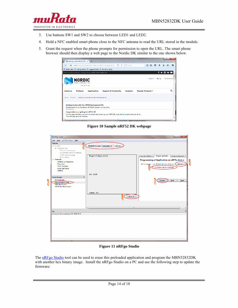
3. Use buttons SW1 and SW2 to choose between LED1 and LED2.
4. Hold a NFC enabled smart phone close to the NFC antenna to read the URL stored in the module.
5. Grant the request when the phone prompts for permission to open the URL. The smart phone browser should then display a web page to the Nordic DK similar to the one shown below.
Figure 10 Sample nRF52 DK webpage
Figure 11 nRFgo Studio
The nRFgo Studio tool can be used to erase this preloaded application and program the MBN52832DK with another hex binary image. Install the nRFgo Studio on a PC and use the following step to update the firmware:

MBN52832DK User Guide
Page 15 of 18
1. Connect the MBN52832DK to the PC with a micro USB cable and wait until the drivers are installed
2. Launch the nRFgo Studio on the computer; in the nRFgo Device Manager pane, select the “nRF5x Programming” option. If this option greyed out, then most likely the drivers are not yet installed. Close nRFgo, wait until the drivers are installed, and launch nRFgo again.
3. Select the correct SEGGER entry with the ID matching the MBN52832DK 4. Click the “Erase all” button to clear everything in the flash memory 5. Select the Program Application tab. Click “Browse...” to select the HEX file to program 6. Unselect the option “Lock entire chip from readback” 7. Click Program, which will program the HEX file onto the selected module
2.4 Application development The MBN52832 Development Kit (MBN52832DK) is designed to facilitate application development using the Nordic nRF52 SDK. The MBN52832DK EVB supports the same J-Link USB-SWD and USB-UART interfaces as those provided by the nRF52 DK, so the software debugging and development process can follow that used for the nRF52 DK. Users can develop their own applications on the EVB by using the following steps:
1. Download and install the latest nRF52 SDK and Keil MDK-ARM or Eclipse tool chains.
2. Create and compile an application
3. Load the application into the EVB
4. Run and debug the application
Go to the Nordic Infocenter for details on nRF52 application development. This section provides the sample configuration for Windows 7 users.
USB to micro-USB cable
Figure 12 Configuration for application development with nRF52 SDK
2.4.1 MBN52832DK compatibility with nRF52 SDK
The EVB has both a 2.4GHz and an NFC chip antenna onboard; it also provides a 32 KHz slow clock along with 2 buttons and 2 LEDs. These interfaces are mapped to the default configuration used for the nRF52 DK, as described in Table 5 below. Any nRF52 SDK application, such as radio_test, that uses only these resources can be downloaded to the EVB and executed with no modification necessary. Additional module IOs can be accessed as described in Section 2.2.5.
nRF52 DK name MBN52832DK
name
nRF52 pin Remark
Button1 SW1 P0.13 Application button
Button2 SW2 P0.14 Application button
LED1 LED1 P0.17 Drive low to turn on LED
LED2 LED2 P0.18 Drive low to turn on LED
NFC1 NFC1 P0.09 NFC antenna input

MBN52832DK User Guide
Page 16 of 18
NFC2 NFC2 P0.10 NFC antenna input
XL1 M_SCLK2 P0.00 32 KHz slow clock
XL2 M_SCLK1 P0.01 32 KHz slow clock
CTS UCTS P0.05 Connect to host CTS/
RxD URxD P0.06 Connect to host RXD
RTS URTS P0.07 Connect to host RTS/
TxD UTxD P0.08 Connect to host TXD
Table 5 MBN52832DK and nRF52 DK signal map
2.4.2 Connect the MBN52832DK Evaluation Board
The EVB connects to the PC through USB. The USB interface provides +5V power as well as individual SWD and UART interfaces to the EVB. This is the same as that provided by the nRF52 DK. Plug the EVB into the development PC with a USB cable; the drivers for these interfaces should automatically load.
2.4.3 Verifying USB Driver Installations
Verify that installation of the drivers was successful by checking the Device Manager window. Follow the steps below to open the Device Manager window:
1. For Win 7, select Windows Start Button->Control Panel->Hardware and sound->Device
Manager. 2. The J-Link driver should be under <computer-name>\Universal Serial Bus controllers as shown in the
screen capture below.
3. The UART Serial Port should be under <computer-name>\Ports (COM & LPT) as shown in the screen capture below.
Figure 13 Screenshot showing installed J-Link drivers

MBN52832DK User Guide
Page 17 of 18
3. EVB schematic The schematic for the module interfaces on the EVB is as shown below.

MBN52832DK User Guide
Page 18 of 18
(END)