wireless sensor networks (wsn) - uni-potsdam.de...msp430 instruction set architecture risc...
TRANSCRIPT

Wireless Sensor Networks (WSN)
Mote Hardware Platforms
M. Schölzel

Goals of this chapter
Survey of the main components of the composition of a node for a wireless sensor network Microcontroller, peripherals, radio, sensors, batteries Integration on a boards
Understanding energy consumption aspects for these components Using low-power modes Mutual dependencies
2

Sensor Node Architecture
Main components of a WSN node Microcontroller: Computation Radio: Communication Sensors/actuators: Measuring/Controlling Memory: Program and data storage Power supply
3
Memory
Microcontroller Sensor(s)/ actuator(s)
Communication device
Power supply

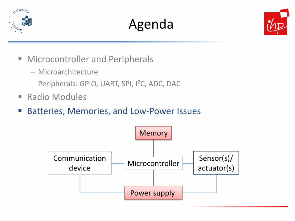
Agenda
Microcontroller and Peripherals − Microarchitecture − Peripherals: GPIO, UART, SPI, I²C, ADC, DAC
Radio Modules Batteries, Memories, and Low-Power Issues
Memory
Microcontroller Sensor(s)/ actuator(s)
Communication device
Power supply

Node Characteristics
Wide variety of mote characteristics: performance: 8-, 16-, 32-bit microcontrollers available memory for program and data available peripherals power consumptions Size, price
5

Example 1 DevDuino Sensor Node V2.0
Board with 8-bit AVR RISC-based microcontroller
Parameter Value
Program Memory Type Flash
Program Memory (KB) 32
CPU Speed (MIPS) 20
RAM Bytes 2048
Data EEPROM (bytes) 1024
Digital Communication Peripherals 1-UART, 2-SPI, 1-I2C
Capture/Compare/PWM Peripherals 1 Input Capture, 1 CCP, 6PWM
Timers 2 x 8-bit, 1 x 16-bit
Comparators 1
Temperature Range (C) -40 to 85
Operating Voltage Range (V)
1.8 to 5.5
Pin Count 32
See also: http://wiki.seeedstudio.com/wiki/DevDuino_Sensor_Node_V2.0_(ATmega_328)
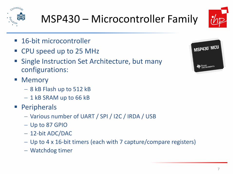
MSP430 – Microcontroller Family
16-bit microcontroller CPU speed up to 25 MHz Single Instruction Set Architecture, but many
configurations: Memory
− 8 kB Flash up to 512 kB − 1 kB SRAM up to 66 kB
Peripherals − Various number of UART / SPI / I2C / IRDA / USB − Up to 87 GPIO − 12-bit ADC/DAC − Up to 4 x 16-bit timers (each with 7 capture/compare registers) − Watchdog timer
7

Example 3 ARM
Freescale MC1322x mote is a platform-in-package using − ZigBee-compatible radio − ARM7TDMI-S microcontroller
ARM7TDMI-S parameters
− 32-bit ARM7TDMI-S microcontroller
8 Freescale Semiconductor Technical Data: Document Number: MC1322x Rev. 1.3 10/2010
Parameter Value
Program Memory Type Flash
Program Memory (KB) 32 to 512
CPU Speed 32-bit microcontroller with 3 stage pipeline running @ 26 MHz
RAM KB 8 to 40
Digital Communication Peripherals UART, SPI,I2C
Capture/Compare/PWM Peripherals external counters (with four capture and four compare channels each), PWM unit (six outputs) and watchdog.
Timers 4 x 16-bit, Low power Real-Time Clock (RTC) with independent power and 32 kHz clock input.
ADC 1 to 2 10-bit ADCs with 6/14 analog inputs with conversion times as low as 2.44 µs
DAC 1 10-bit DAC
Temperature Range (C) -40 to 105
Operating Voltage Range (V) 2.0 to 3.6
Pin Count 99 pin LGA package

Memory Mapping in Microcontrollers
Different types of memory on-chip mapped into a single address space Memory Mapped IO:
− Accesses to memory addresses is redirected to registers of peripherals
Data Memory for fast access:
− SRAM − EEPROM − Flash − NVRam
Program Memory
− OTP-ROM − EPROM − Flash
External Memory (off-chip), several MBytes, usually not mapped in
address space: − DRAM − Flash
9
Memory Mapped
I/O
Program Memory
0x0000
0x3FFFF
External Memory
Data Memory
…
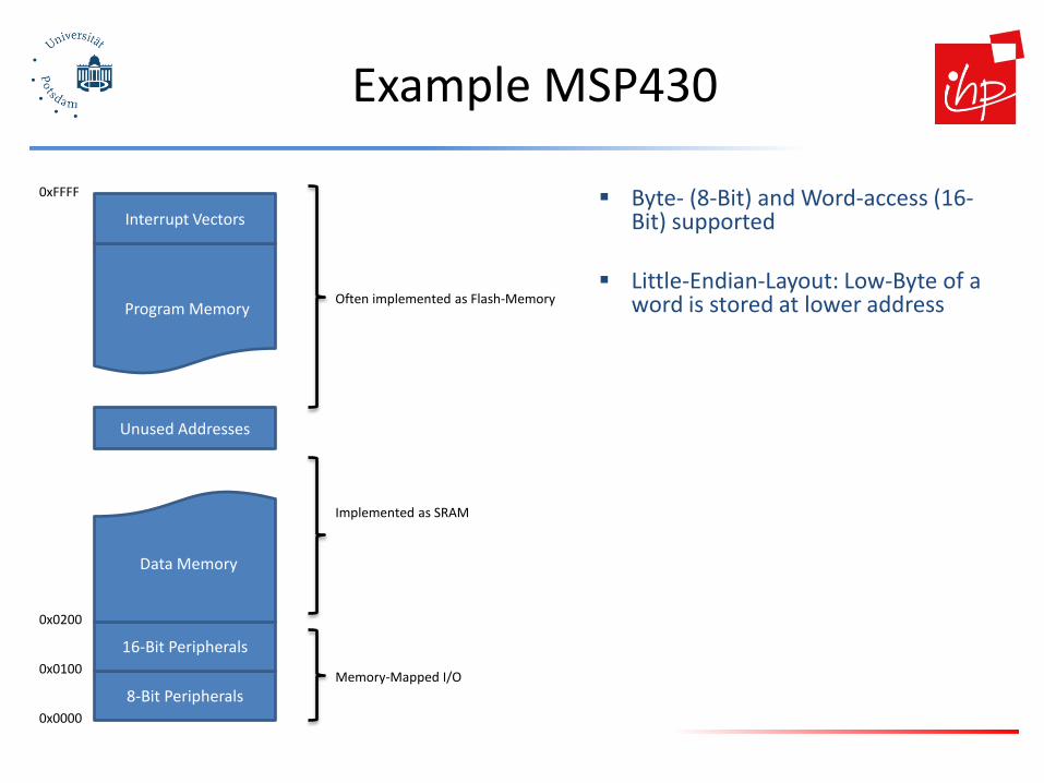
Example MSP430
Byte- (8-Bit) and Word-access (16-Bit) supported
Little-Endian-Layout: Low-Byte of a word is stored at lower address
8-Bit Peripherals 0x0000
0x0100 16-Bit Peripherals
0x0200
Interrupt Vectors
Data Memory
Program Memory
Unused Addresses
0xFFFF
Often implemented as Flash-Memory
Implemented as SRAM
Memory-Mapped I/O

MSP430 Microarchitecture and Memory-Mapped I/O
Each peripheral uses a unique address space
normal memory operations can be used for reading/writing data from/to peripherals
11
Clock Module
MSP430 CPU
MAB
MDB
Flash RAM Peri-
pherial 2
Peri-pherial
n
ACLK
SMCLK
Peri-pherial
1
MCLK
to peripherals
MCLK: Master Clock ACLK: Auxiliary Clock SMCLK: Secondary Master Clock

MSP430-CPU Microarchitecture
Register R4 to R15 are general purpose registers
Registers 0 to 3 have special meaning:
− PC…Program Counter
(LSB is always 0)
− SP…Stack Pointer (LSB is always 0)
− SR…Status Register (contains flags, controls low power modes and interrupts)
− CG2…Constant Generator (can be used for generating special constants)
ALU
S-Reg D-Reg
Alu-Mux
Register File
R0 (PC) R1 (SP) R2 (SR)
R3 (CG2) R4 R5 R6 R7 R8 R9
R10 R11 R12 R13 R14 R15 src dst
Memory Data Bus (MDB)
IR
Sign-Ext
Addr-Mux
0 +1 +2 -2
Adder
MAR-Mux
Memory Address Bus (MAB)
Flags
MSP430 CPU

MSP430-CPU Microarchitecture
INSTRUCTION FETCH − Obtain the next instruction from
memory
DECODE − Examine the instruction, and
determine how to execute it
SOURCE OPERAND FETCH − Load source operand
DESTINATION OPERAND FETCH
− Load destination operand
EXECUTE − Carry out the execution of the
instruction
STORE RESULT − Store the result in the designated
destination
ALU
S-Reg D-Reg
Alu-Mux
Register File
R0 (PC) R1 (SP) R2 (SR)
R3 (CG2) R4 R5 R6 R7 R8 R9
R10 R11 R12 R13 R14 R15 src dst
Memory Data Bus (MDB)
IR
Sign-Ext
Addr-Mux
0 +1 +2 -2
Adder
MAR-Mux
Memory Address Bus (MAB)
Flags
MSP430 CPU

MSP430 Instruction Set Architecture
RISC architecture
Opcode is composed of 1 to 3 words
2-Address-Architecture: − One source operand is used as destination operand − Memory operands are allowed
Three classes of operations:
− Single-operand-arithmetic − Two-operand-arithmetic − Branch operations

MSP430 Single-Operand-Arithmetic
Bits 15..10 are fixed to 000100 Bits 9..7 are used to encode up to 8 operations Bit 6 (B/W):
− 0 .. Byte operation − 1 .. Word operation
Bits 5..4 encode the addressing mode Bits 3..0 encode source/destination operand

MSP430 Two-Operand-Arithmetic
Bits 15..12 are used to encode the opcode and are distinct from 000 and 001 Bits 11..8 encode the source register Bits 7 (Ad) and 5..4 (As) encode the addressing mode Bit 6 (B/W):
− 0 .. Byte operation − 1 .. Word operation
Bits 3..0 encode source/destination operand
mov.w #label,PC ;branch to address label (lower 64KB) mova #label,PC ;branch to address label (lower 1MB memory) mov.w label,pc ;branch to address in memory word label mov.w @r14,PC ;branch indirect to address in R14 adda #4,PC ;skip two words

MSP430 Branch-Operation
Bits 15..13 are fixed to 001 Bits 12..10 encode the branch-condition Bits 0..9 encode a 10-bit offset which is added to the current PC

Examples
move an immediate value into a register/memory word − mov.w #0x2F,r8 − mov.w #0x8000,myData
set a bit in an register/memory word
− bis.w #0x8000,r8 − bis.w #0x4000,myData
clear a bit in a register/memory word
− bic.w #0x2,r8 − bic.w #0x8000,myData
invert a bit in a register/memory word
− xor.w #0x000F,r8 − xor.w #0x4200,myData

Agenda
Microcontroller and Peripherals − Microarchitecture − Peripherals: GPIO, UART, SPI, I²C, ADC, DAC
Radio Modules Batteries, Memories, and Low-Power Issues
Memory
Microcontroller Sensor(s)/ actuator(s)
Communication device
Power supply
Peripherals
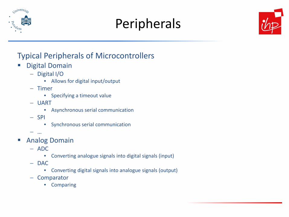
Typical Peripherals of Microcontrollers Digital Domain
− Digital I/O • Allows for digital input/output
− Timer • Specifying a timeout value
− UART • Asynchronous serial communication
− SPI • Synchronous serial communication
− … Analog Domain
− ADC • Converting analogue signals into digital signals (input)
− DAC • Converting digital signals into analogue signals (output)
− Comparator • Comparing
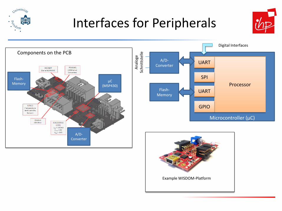
Microcontroller (µC)
Interfaces for Peripherals
Processor
A/D-Converter UART
Flash-Memory
SPI
UART
GPIO
Flash-Memory
µC (MSP430)
A/D-Converter
Example WISDOM-Platform
Components on the PCB Digital Interfaces
Anal
oge
Schn
ittst
elle
Digital I/O – MSP430
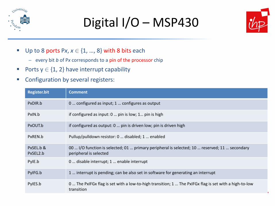
Up to 8 ports Px, x Î {1, …, 8} with 8 bits each − every bit b of Px corresponds to a pin of the processor chip
Ports y Î {1, 2} have interrupt capability Configuration by several registers:
Register.bit Comment
PxDIR.b 0 … configured as input; 1 … configures as output
PxIN.b if configured as input: 0 … pin is low; 1… pin is high
PxOUT.b if configured as output: 0 … pin is driven low; pin is driven high
PxREN.b Pullup/pulldown resistor: 0 … disabled; 1 … enabled
PxSEL.b & PxSEL2.b
00 … I/O function is selected; 01 … primary peripheral is selected; 10 … reserved; 11 … secondary peripheral is selected
PyIE.b 0 … disable interrupt; 1 … enable interrupt
PyIFG.b 1 … interrupt is pending; can be also set in software for generating an interrupt
PyIES.b 0 … The PxIFGx flag is set with a low-to-high transition; 1 … The PxIFGx flag is set with a high-to-low transition
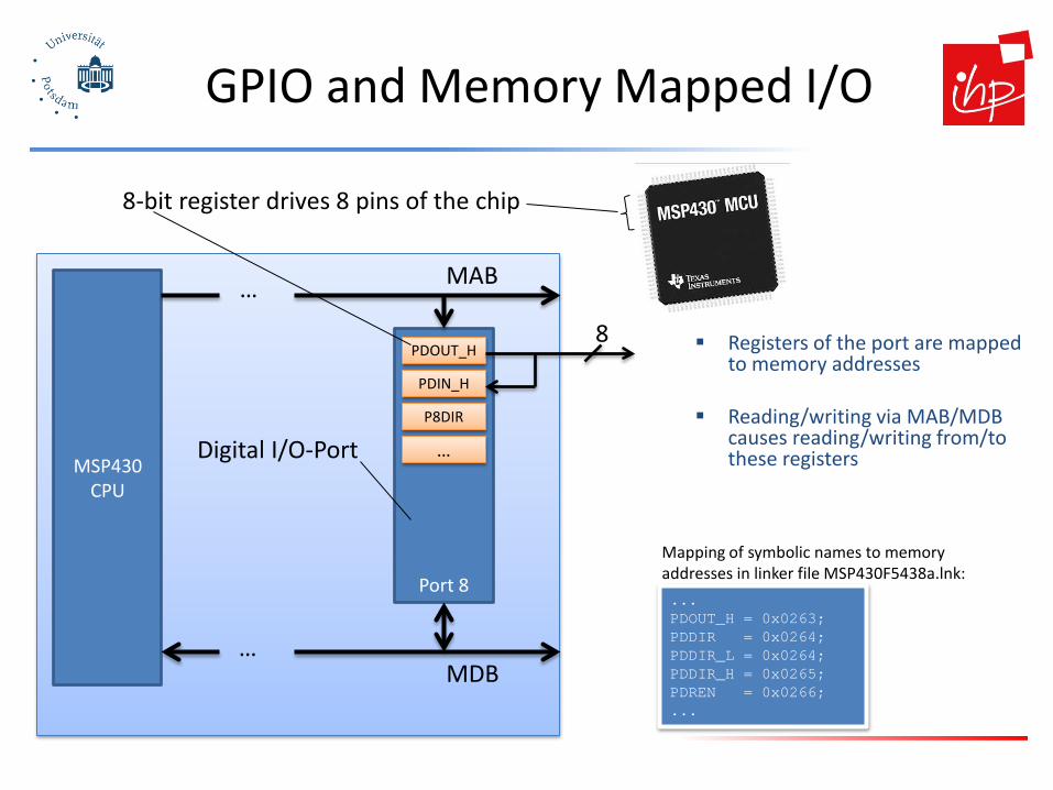
GPIO and Memory Mapped I/O
Registers of the port are mapped to memory addresses
Reading/writing via MAB/MDB causes reading/writing from/to these registers MSP430
CPU
MAB
MDB
Port 8
PDOUT_H
PDIN_H
P8DIR
…
…
…
8
... PDOUT_H = 0x0263; PDDIR = 0x0264; PDDIR_L = 0x0264; PDDIR_H = 0x0265; PDREN = 0x0266; ...
Mapping of symbolic names to memory addresses in linker file MSP430F5438a.lnk:
8-bit register drives 8 pins of the chip
Digital I/O-Port
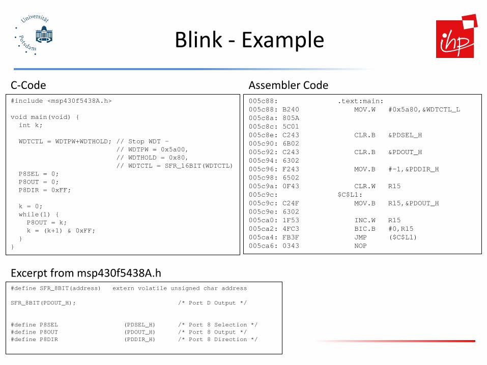
Blink - Example
#include <msp430f5438A.h> void main(void) { int k; WDTCTL = WDTPW+WDTHOLD; // Stop WDT – // WDTPW = 0x5a00, // WDTHOLD = 0x80, // WDTCTL = SFR_16BIT(WDTCTL) P8SEL = 0; P8OUT = 0; P8DIR = 0xFF; k = 0; while(1) { P8OUT = k; k = (k+1) & 0xFF; } }
005c88: .text:main: 005c88: B240 MOV.W #0x5a80,&WDTCTL_L 005c8a: 805A 005c8c: 5C01 005c8e: C243 CLR.B &PDSEL_H 005c90: 6B02 005c92: C243 CLR.B &PDOUT_H 005c94: 6302 005c96: F243 MOV.B #-1,&PDDIR_H 005c98: 6502 005c9a: 0F43 CLR.W R15 005c9c: $C$L1: 005c9c: C24F MOV.B R15,&PDOUT_H 005c9e: 6302 005ca0: 1F53 INC.W R15 005ca2: 4FC3 BIC.B #0,R15 005ca4: FB3F JMP ($C$L1) 005ca6: 0343 NOP
C-Code Assembler Code
#define SFR_8BIT(address) extern volatile unsigned char address SFR_8BIT(PDOUT_H); /* Port D Output */ #define P8SEL (PDSEL_H) /* Port 8 Selection */ #define P8OUT (PDOUT_H) /* Port 8 Output */ #define P8DIR (PDDIR_H) /* Port 8 Direction */
Excerpt from msp430f5438A.h

Clocks in the MSP430
Three clocks are available that can be used form different peripherals
Various oscillator-sources exist to generate these clocks Clock
Module
MSP430 CPU
MAB
MDB
Flash RAM Peri-
pherial 2
Peri-pherial n
ACLK
SMCLK
Peri-pherial 1
MCLK
to peripherals

Basic Clock Module: Available Clocks
Three clocks are available:
MCLK: MCLK is divided by 1, 2, 4, or 8. MCLK is used by the CPU and system.
SMCLK: SMCLK is divided by 1, 2, 4, or 8. SMCLK is software selectable for individual peripheral modules.
ACLK: ACLK be divided by 1, 2, 4, or 8. ACLK is software selectable for individual peripheral modules.
Oscillator Sources
LFXT1CLK VLOCLK
LFXT1CLK [XT2CLK] DCOCLK
LFXT1CLK [XT2CLK] DCOCLK

Basic Clock Module: Oscillators
Various oscillator-sources exist that can generate various frequencies at various power consumptions: LFXT1CLK: Low-frequency/high-frequency oscillator
that can be used with low-frequency watch crystals or external clock sources of 32768 Hz or with standard crystals, resonators, or external clock sources in the 400-kHz to 16-MHz range.
XT2CLK: Optional high-frequency oscillator that can be used with standard crystals, resonators, or external clock sources in the 400-kHz to 16-MHz range.
DCOCLK: Internal digitally controlled oscillator (DCO).
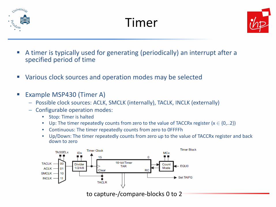
Timer
A timer is typically used for generating (periodically) an interrupt after a specified period of time
Various clock sources and operation modes may be selected
Example MSP430 (Timer A) − Possible clock sources: ACLK, SMCLK (internally), TACLK, INCLK (externally) − Configurable operation modes:
• Stop: Timer is halted • Up: The timer repeatedly counts from zero to the value of TACCRx register (x Î {0,..2}) • Continuous: The timer repeatedly counts from zero to 0FFFFh • Up/Down: The timer repeatedly counts from zero up to the value of TACCRx register and back
down to zero
to capture-/compare-blocks 0 to 2

Example for Usage of Capture-/Compare block
In capture mode current timer value is captured in capture register up on an event the event is typically an external trigger, e.g. rising/falling edge on an external pin
− The timer value is copied into the TACCRx register − The interrupt flag CCIFG is set
In compare mode compare mode is used
to generate PWM output signals or interrupts at specific time intervals
If timer register is equal to the value of the compare register: − interrupt is raised − output signal is set according
to the current output mode
from 16-bit TA register
to output logic
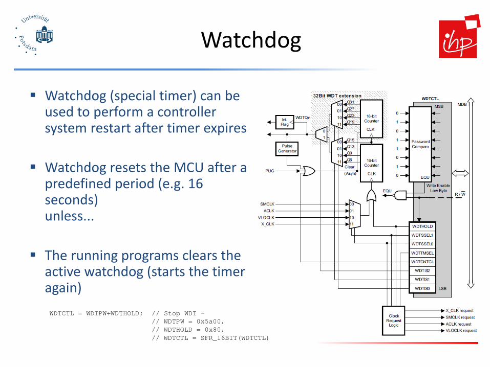
Watchdog
Watchdog (special timer) can be used to perform a controller system restart after timer expires
Watchdog resets the MCU after a predefined period (e.g. 16 seconds) unless...
The running programs clears the active watchdog (starts the timer again)
WDTCTL = WDTPW+WDTHOLD; // Stop WDT – // WDTPW = 0x5a00, // WDTHOLD = 0x80, // WDTCTL = SFR_16BIT(WDTCTL)

Device 2
UART
UART (Universal Asynchronous Transceiver and Transmitter) Point-to-Point connection between 2 devices
bi-directional, full duplex
only two wires
no clock signal (asynchronous)
Devi
ce 1
Transmitter Block (TX)
Receiver Block (RX)
Receiver Block (RX)
Transmitter Block (TX)

UART Datenübertragung Zu übertragende Daten werden
− in einen Rahmen verpackt − und dann der Rahmen bitweise übertragen
Transmitter und Receiver müssen in folgenden Parametern übereinstimmen:
− Baudrate: Übertragene Zeichen (hier Bits) pro Sekunde (9600 Baud bedeutet 0,00010417 Sekunden pro Bit) − Stoppbits: 1, 1.5 oder 2 − Datenbits: 5,6,7, oder 8 − Parität: gerade oder ungerade (ergänzt die Anzahl der 1en in den Datenbits zu einer geraden/ungeraden Anzahl)
Rahmenformat:
Beispiel für Datenübertragung:
Start Bit (immer 0)
Bit 0 LSB Bit 1 Bit n-1 Bit n
MSB Paritätsbit Stoppbit
1 1 0 0 0 1 1
Ruhe Daten
Parit
ät
Star
tbit
1
Stop
pbit Ruhe
0 1 0 0 1 1 1
Daten
Parit
ät
Star
tbit
0
Stop
pbit Ruhe
… Rahmenbits
Datenbits
TX
0 0 1 0 1 1
Byte 1 Byte 2

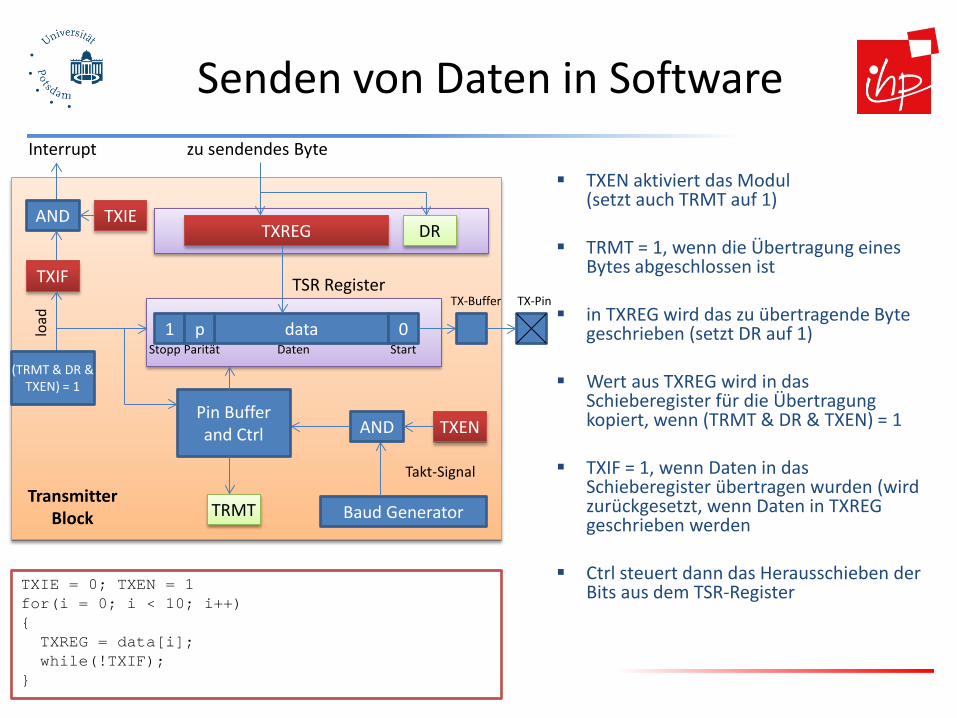
Aufbau des Transmitters
TXEN aktiviert das Modul (setzt auch TRMT auf 1)
TRMT = 1, wenn die Übertragung eines Bytes abgeschlossen ist
in TXREG wird das zu übertragende Byte geschrieben (setzt DR auf 1)
Wert aus TXREG wird in das Schieberegister für die Übertragung kopiert, wenn (TRMT & DR & TXEN) = 1
TXIF = 1, wenn Daten in das Schieberegister übertragen wurden (wird zurückgesetzt, wenn Daten in TXREG geschrieben werden
Ctrl steuert dann das Herausschieben der Bits aus dem TSR-Register
TXREG
zu sendendes Byte
data 1 0
TXIF
Interrupt
load
Baud Generator
Takt-Signal
TXEN AND Pin Buffer and Ctrl
AND TXIE
TRMT
DR De
vice
1 Transmitter
Block (TX)
Receiver Block (RX)
(TRMT & DR & TXEN) = 1
Stopp p
Parität Daten Start
TX-Buffer TX-Pin
Transmitter Block
TSR Register
Senden von Daten in Software
TXEN aktiviert das Modul (setzt auch TRMT auf 1)
TRMT = 1, wenn die Übertragung eines Bytes abgeschlossen ist
in TXREG wird das zu übertragende Byte geschrieben (setzt DR auf 1)
Wert aus TXREG wird in das Schieberegister für die Übertragung kopiert, wenn (TRMT & DR & TXEN) = 1
TXIF = 1, wenn Daten in das Schieberegister übertragen wurden (wird zurückgesetzt, wenn Daten in TXREG geschrieben werden
Ctrl steuert dann das Herausschieben der Bits aus dem TSR-Register
TXREG
zu sendendes Byte
data 1 0
TXIF
Interrupt
load
Baud Generator
Takt-Signal
TXEN AND Pin Buffer and Ctrl
AND TXIE
TRMT
DR
TXIE = 0; TXEN = 1 for(i = 0; i < 10; i++) { TXREG = data[i]; while(!TXIF); }
(TRMT & DR & TXEN) = 1
Stopp p
Parität Daten Start
TX-Buffer TX-Pin
Transmitter Block
TSR Register

Receiver Block
Aufbau des Receivers Takt des Empfängers ist n Mal höher als der
des Senders
Data Recovery prüft RX-Leitung auf Übergang auf 0 (Startbit) mit n-fach höherer Taktrate
Receiver wartet dann n/2 Takte und sampelt dann alle n Takte die nächsten Bits, die in das TSR-Register geschoben werden
Wurde das Stoppbit ins TSR-Register geschoben, dann wird der Datenwert in das RXREG kopiert und RXDR auf 1 gesetzt
Interrupt
Takt-Generator
AND
RXIE
Data Recovery and Ctrl
n x Takt-Signal
RXREG RXDR
RXEN AND
1 1 0
Ruhe
Star
tbit
TX 0
RX-Pin
Takt des Senders
Takt des Empfängers
Start erkannt Wert auf RX-Leitung prüfen
data 1 0 Stopp
p Parität Daten Start
Empfangene Daten
Devi
ce 1
Transmitter Block (TX)
Receiver Block (RX)

Receiver Block
Empfangen von Daten in Software Takt des Empfängers ist n Mal höher als der des
Senders
Data Recovery prüft RX-Leitung auf Übergang auf 0 (Startbit) mit n-fach höherer Taktrate
Receiver wartet dann n/2 Takte und sampelt dann alle n Takte die nächsten Bits, die in das TSR-Register geschoben werden
Wurde das Stoppbit ins TSR-Register geschoben, dann wird der Datenwert in das RXREG kopiert und RXDR auf 1 gesetzt
RXDR wird durch Auslesen von RXREG auf 0 gesetzt
Interrupt
Takt-Generator
AND
RXIE
RXIE = 0; RXEN = 1 for(i = 0; i < 10; i++) { while(!RXDR); data[i] = RXREG }
Data Recovery and Ctrl
n x Takt-Signal
RXREG RXDR
RXEN AND
1 1 0
Ruhe
Star
tbit
TX 0
RX-Pin
Takt des Senders
Takt des Empfängers
Start erkannt Wert auf RX-Leitung prüfen
data 1 0 Stopp
p Parität Daten Start
Empfangene Daten

Integration in den Prozessor
Wie kann die Software auf die UART-Register zugreifen? Peripherie-Blöcke (Speicher, UART, SPI, GPIO) bekommen
Adressbereiche zugewiesen (Memory-Mapped I/O)
Lese-/Schreibzugriffe des Prozessors auf diese Adressbereiche werden vom entsprechenden Peripherie-Block behandelt
Beispiel
− TXREG von UART1 ist auf Adresse 0x1C0 abgebildet
µC
UART
SPI
UART
GPIO
Prozessor
Adress- und Command-Bus
Daten-Bus
UART 1
TXREG
= 0x1C0 ?
wrE
nbl Speicher
Adressbereich 0x200 bis 0x4000
UART 2
TXREG
= 0x1E0 ?
wrE
nbl
SPI GPIO
TXIE = 0; TXEN = 1 for(i = 0; i < 10; i++) { TXREG = data[i]; while(!TXIF); }
uint8* p = 0x1c0; *p = data[i];
REG

Slave 1 Mas
ter
SPI
SCLK
CS1
MOSI
MISO
SCLK
CS
MOSI
MISO
CS2
SPI (Serial Peripheral Interface ) Serieller Datenaustausch zwischen einem Master
und mehreren Slaves − Master wählt über CSi Slave i aus
bidirektional, vollduplex
mind. 4 Leitungen
Taktsignal wird verwendet (synchron)
− Master legt den Takt fest − Master und Slave senden gleichzeitig Daten
Slave n
SCLK
CS
MOSI
MISO
…

SPI Implementation
Implementation of sender/receiver module Slave 1 M
aste
r
SCLK
MOSI
MISO 8-bit shift register 8-bit shift register
SPI Clock Generator
MSB MSB
CS
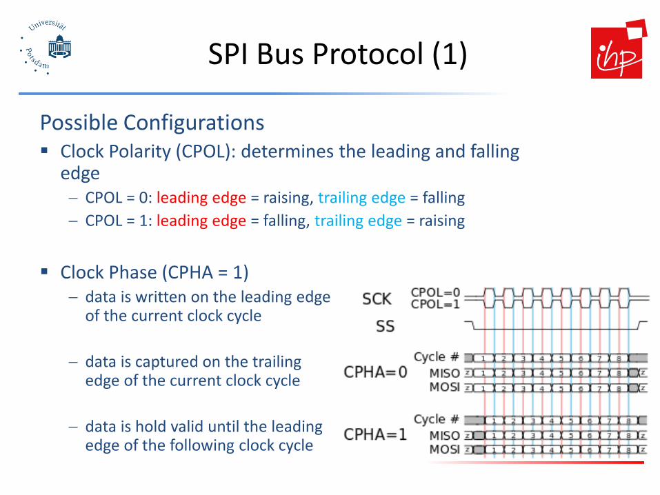
SPI Bus Protocol (1)
Possible Configurations Clock Polarity (CPOL): determines the leading and falling
edge − CPOL = 0: leading edge = raising, trailing edge = falling − CPOL = 1: leading edge = falling, trailing edge = raising
Clock Phase (CPHA = 1)
− data is written on the leading edge of the current clock cycle
− data is captured on the trailing edge of the current clock cycle
− data is hold valid until the leading edge of the following clock cycle
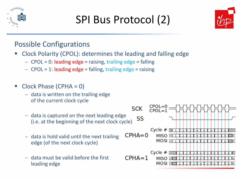
SPI Bus Protocol (2)
Possible Configurations Clock Polarity (CPOL): determines the leading and falling edge
− CPOL = 0: leading edge = raising, trailing edge = falling − CPOL = 1: leading edge = falling, trailing edge = raising
Clock Phase (CPHA = 0)
− data is written on the trailing edge of the current clock cycle
− data is captured on the next leading edge (i.e. at the beginning of the next clock cycle)
− data is hold valid until the next trailing edge (of the next clock cycle)
− data must be valid before the first leading edge

I²C Interface
I²C (Inter-Integrated Circuit) Serial data transfer between a master and multiple slaves
− Shared bus with addressing − slave is selected by the master − multi-master possible
bi-directional, half-duplex
2 wires only
− SCL … Serial Clock − SDA … Serial Data
Clock signal is generated from the master
mode maximum data rate
standard mode 0,1 Mbit/s
fast mode 0,4 Mbit/s
fast mode plus 1,0 Mbit/s
high speed mode 3,4 Mbit/s
ultra fast-mode 5,0 Mbit/s Master Slave 1 Slave n …
Vdd
SDA
SCL
Pull-up resistors: force SDA and SCL to high

I²C - Addressing
Every I²C device has a 7-bit address − up to 112 devices on a single bus − 16 addresses reserved for special purposes
• some of them are used for later support of 10 bit addresses − Manufacturer of the device assigns the address
• devices with the same address cannot operate on the same bus • sometimes lower 3 bits of the address can be assigned by pin settings
First byte on the bus is sent from the master and contains
slave-address and direction for communication − bit0 to bit6 … address − bit7 = 0 (master sends data to slave) − bit7 = 1 (master receives data from slave)
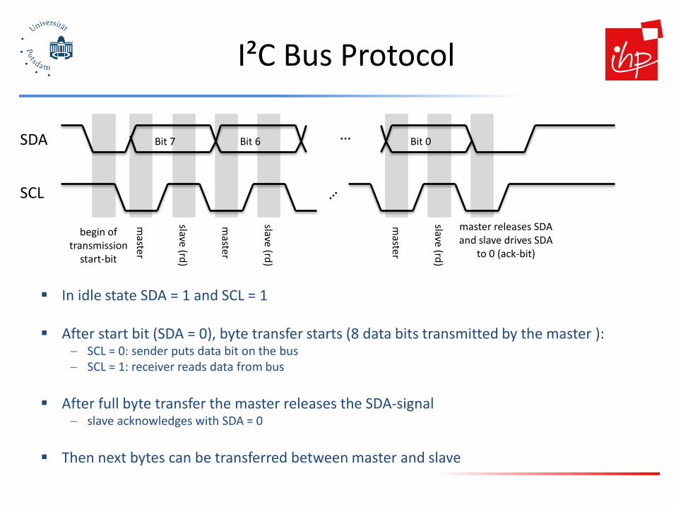
I²C Bus Protocol
In idle state SDA = 1 and SCL = 1
After start bit (SDA = 0), byte transfer starts (8 data bits transmitted by the master ): − SCL = 0: sender puts data bit on the bus − SCL = 1: receiver reads data from bus
After full byte transfer the master releases the SDA-signal
− slave acknowledges with SDA = 0
Then next bytes can be transferred between master and slave
SDA
SCL
begin of transmission
start-bit
Bit 7 Bit 6 Bit 0 …
master releases SDA and slave drives SDA
to 0 (ack-bit)
master
slave (rd)
master
slave (rd)
master
slave (rd)

ADCs und DACs
Analoge Signale sind zeit- und wertekontinuierlich Digitale Systeme sind aufgrund des Taktes und der endlichen Binärdarstellung
− zeitdiskret − wertediskret
A/D-Wandler müssen analoge Werte in zugehörige Binärdarstellung umwandeln − tun das nur zu diskreten Zeitpunkten
Sample / Hold A/D
Digitales Verarbeitungs-
System D/A Stellglied
(Aktor)
Analoge Spannung
Analoge Spannung
Quelle (z. B.
Sensor)
Span
nung
Zeit
Digitale Werte
Digitale Werte

Invertierender Operationsverstärker (OPV)
OPV versucht seine Eingänge auf dem gleiche Potential zu halten (vgl. gestrichelte Linie Udiff = 0)
R1 befindet sich zwischen Ue und virtueller Masse; es fließt damit ein Strom von I = Ue/R1
Weil der OPV einen extrem hohen Eingangswiderstand hat, muss I auch durch R2 fließen; also Ua = -I*R2
Es ergibt sich: Ua = -Ue/R1*R2
Ist R1 variabel, dann kann Ua über R1 gesteuert werden.
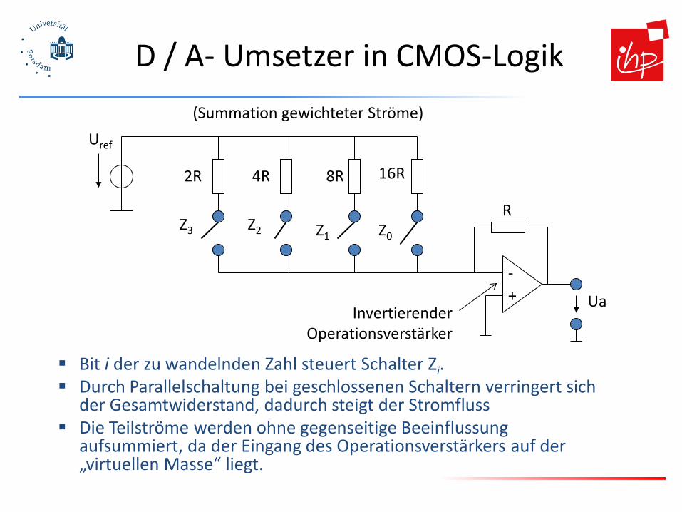
D / A- Umsetzer in CMOS-Logik
Bit i der zu wandelnden Zahl steuert Schalter Zi. Durch Parallelschaltung bei geschlossenen Schaltern verringert sich
der Gesamtwiderstand, dadurch steigt der Stromfluss Die Teilströme werden ohne gegenseitige Beeinflussung
aufsummiert, da der Eingang des Operationsverstärkers auf der „virtuellen Masse“ liegt.
(Summation gewichteter Ströme)
2R 4R 8R 16R
- + Ua
R
Uref
Z1 Z2 Z3 Z0
Invertierender Operationsverstärker

Diskretisierung der Signalwerte
n
x (n)
0 T
n
x (n)
0 T
Abtasten des analogen Signals zu diskreten Zeitpunkten mit Periode T (Abtastrate/Samplerate = 1/T)
A/D Umsetzung des analogen Spannungswertes in einen zugehörigen digitalen Wert
Abtast- und Halteglied
A/D-Umsetzung

Abtast-und Halteglieder (Prinzip)
Ue
+ -
Nicht-invertierender Operationsverstärker
+ -
Eingangs- spannung
Ausgangs-spannung (zum A/D Umsetzer)
Out Schalter
Schaltsignal
n
p
Schalteraufbau (Transmission Gate)
In Schalter
periodisch betätigter Schalter

A / D- Umsetzung
Die Verfahren sind grundsätzlich fehlerbehaftet: Quantisierungsfehler
Quantisierungsfehler entstehen, weil nur eine endliche Anzahl digitaler Werte für die Darstellung unendlich vieler analoger Werte bereitstehen
Wichtig für Umsetzung: − ULSB ist der Spannungsunterschied, der dem Unterschied zwischen arithmetischen
„null“ –Wert auf der digitalen Seite und der „1“ des niederwertigsten Bits entspricht.
0 V
Uref
000 001 010 011
111
anal
oge
Wer
te
digi
tale
Dar
stel
lung
110
100 101
ULSB
Z
Ue
Ua
Quantisierungsfehler = |Ue – Ua|
Z = Ue / ULSB
Ua = Z * ULSB
Ue analoge Eingangsspannung

A/D- Umsetzung (Verfahren)
Es gibt 3 grundsätzliche Verfahren: Parallelverfahren (word at a time) Wägeverfahren (digit at a time) Zählverfahren (level at a time)
1 10 100 1k 10k 100k 1M 10M 100M f / Hz
Auflösung in Bit
0 2 4 6 8
10 12 14 16 18 20
Wäge- verfahren
Parallel- verfahren
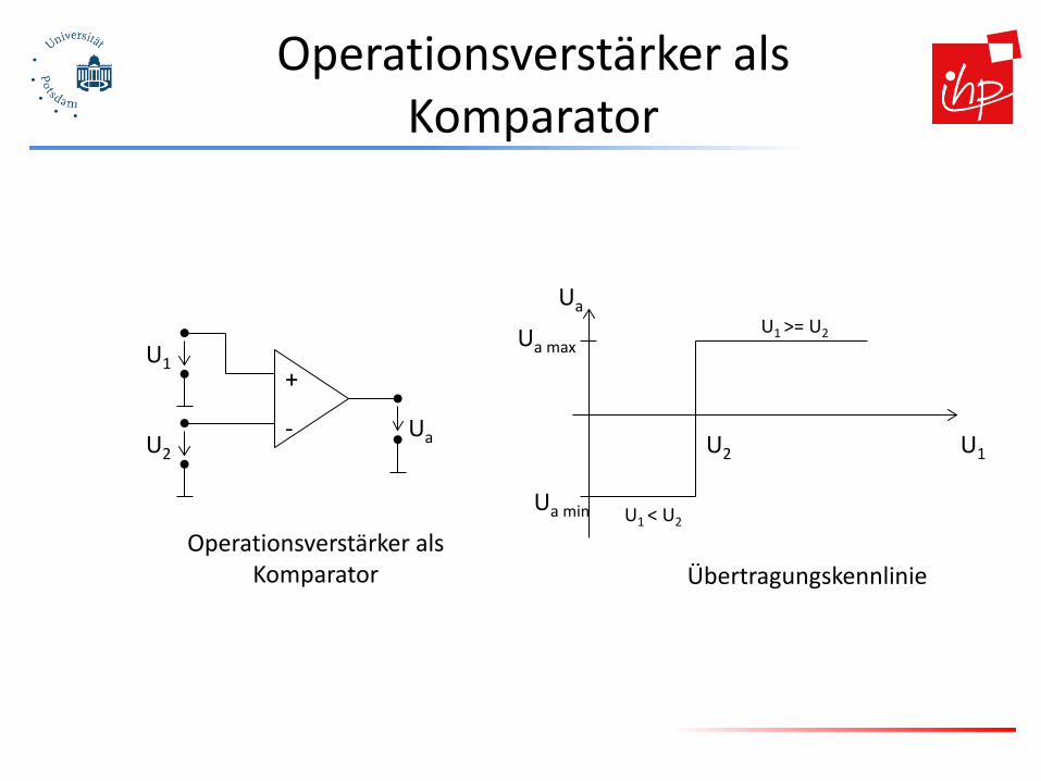
Operationsverstärker als Komparator
+
- U2
U1
Ua U1
Ua
Ua min
Ua max
U2
Übertragungskennlinie Operationsverstärker als
Komparator
U1 < U2
U1 >= U2

Paralleler A / D- Umsetzer (3 Bit)
Prioritäts- dekoder
Q 1D C1
Q 1D C1
Q 1D C1
Q 1D C1
Q 1D C1
Q 1D C1
Q 1D C1
+ -
+ -
+ -
+ -
+ -
+ -
+ -
Z2
Z1
Z0
Uref
Takt
Ue
½ R
R
R
R
R
R
R
½ ULSB
3/2 ULSB
5/2 ULSB
7/2 ULSB
9/2 ULSB
11/2 ULSB
13/2 ULSB
7 ULSB
x1
x2
x3
x4
x5
x6
x7 Ue = 3 ULSB
1
1
1
0
0
0
0
½ R
000 001 010 011
111 110
100 101
Ue
1 2 3

A/ D- Wandler nach dem Wägeverfahren
Bits im Approximationsregister Z werden schrittweise wie folgt bestimmt: Z := 0 Höchstwertiges Bit wird probehalber auf 1 gesetzt Falls U(z) > Ue, dann wird es wieder gelöscht, sonst bleibt
es gesetzt Dieser Vorgang wird dann mit dem nächst niedrigeren Bit
in Z wiederholt.
Abtast- und Halteglied
Ue
D/A- Umsetzer
+
-
Sukzessives Approximations-
register Z D
Z
U(z)
Uref
Taktgenerator
000 001 010 011
111 110
100 101
Takt 1 2 3 4
Ue

A / D-Wandler nach dem Zählverfahren
Komparator vergleicht Wert des Zählers mit Wert des Haltegliedes.
Wenn U(z) > Ue, dann Zähler dekrementieren, sonst inkrementieren
Abtast- und Halteglied
Ue
DA- Umsetzer
+
-
Vorwärts- / Rückwärts-
Zähler U /D
Z
U(z)
Uref
Taktgenerator
000 001 010 011
111 110
100 101
Takt 1 2 3
Ue

Anbindung an den Mikrocontroller
Integration auf dem Chip Anbindung wie eine UART oder SPI
Schnittstelle Register können über Memory-Mapped
I/O geschrieben/gelesen werden − Setzen verschiedener Konfigurationen − Starten der A/D-Wandlung − Auslesen des gewandelten Wertes − Interrupt-Kontrolle
Anbindung über serielle Schnittstelle ADC ist ein separater Chip Kommunikation z.B. über UART es existiert ein Protokoll für die
Kommunikation
Prozessor UART 1 A/D-Wandler
Mikrocontroller (µC)
Prozessor A/D- Wandler
UART SPI
UART
GPIO
Anal
oge
Schn
ittst
elle
Reg1 Regn
UART

Beispiel ADC im ATmega8
signed long readADC() { // Kontrollregister initialisieren ADC12CTL0 = SHT0_6 + SHT1_6 + REFON + ADC12ON; ... // ADC starten ADC12CTL0 |= ADC12SC + ENC; // Warten bis die Konvertierung abgeschlossen while (ADC12CTL0 & ADC12SC); // Digitalwert auslesen return ADC12MEM0; }
Eine Wandlung wird gestartet, indem eine 1 in das ADC Start Conversion (ADSC) Bit geschrieben wird
Bit bleibt während der Wandlung gesetzt
wird nach Ende der Wandlung automatisch durch die Hardware wieder gelöscht
Danach kann der digitale Wert aus dem ADC Data Register ausgelesen werden

A/D-Wandler Interface über UART
ADC-Modul stellt Zugriff auf interne Register über UART-Protokoll bereit
Mögliche Realisierung: − Jedes interne Register bekommt eine Adresse zugewiesen − Über UART-Schnittstelle können zwei Byte (Adresse, Wert) versendet werden, um
Kontrollregister mit Wert zu beschreiben
Bei Ende einer Konvertierung Übertragung des Wertes über UART − Prozessor kann auf Empfangen eines Wertes warten
signed long readADCviaUART() { // Kontrollregister Adresse senden sendByteUART0(ADC12CTL0); // Wert für Kontrollregister 0x01 senden sendByteUART0(SHT0_6 + SHT1_6 + REFON + ADC12ON); ... // Warten bis Digitalwert zurückgesendet wird return receiveByteUART0(); }
signed long readADC() { // Kontrollregister initialisieren ADC12CTL0 = SHT0_6 + SHT1_6 + REFON + ADC12ON; ... // ADC starten ADC12CTL0 |= ADC12SC + ENC; // Warten bis die Konvertierung abgeschlossen while (ADC12CTL0 & ADC12SC); // Digitalwert auslesen return ADC12MEM0; }

Agenda
Microcontroller and Peripherals − Microarchitecture − Peripherals: GPIO, UART, SPI, I²C, ADC, DAC
Radio Modules Batteries, Memories, and Low-Power Issues
Memory
Microcontroller Sensor(s)/ actuator(s)
Communication device
Power supply

Radio The radio is the communication device of a sensor node using radio
frequencies for transmission − other transceivers are possible (light, ultra-sound, etc.) − we will focus on radio frequencies
Radio Module = Radio + Microcontroller
− Simplifies the communication with the radio
Motes microprocessor and radio often connected via UART or SPI
Mote
UART
Base-band
Analogue Frontend
(AFE)
Micro-con-
troller
Data/Commands
Data
Radio
Radio Module
Radio Frontend (RF)
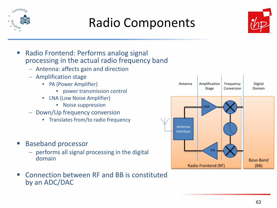
Radio Components
Radio Frontend: Performs analog signal processing in the actual radio frequency band − Antenna: affects gain and direction − Amplification stage
• PA (Power Amplifier) • power transmission control
• LNA (Low Noise Amplifier) • Noise suppression
− Down/Up frequency conversion • Translates from/to radio frequency
Baseband processor − performs all signal processing in the digital
domain
Connection between RF and BB is constituted by an ADC/DAC
63
Antenna Interface
Base-Band (BB)
Frequency Conversion
LNA
PA
Amplification Stage
Antenna Digital Domain

Radio spectrum for communication
Which part of the electromagnetic spectrum is used for communication Not all frequencies are equally suitable for all tasks – e.g., wall penetration,
different atmospheric attenuation (oxygen resonances, …)
64
• VLF = Very Low Frequency UHF = Ultra High Frequency • LF = Low Frequency SHF = Super High Frequency • MF = Medium Frequency EHF = Extra High Frequency • HF = High Frequency UV = Ultraviolet Light • VHF = Very High Frequency
1 Mm 300 Hz
10 km 30 kHz
100 m 3 MHz
1 m 300 MHz
10 mm 30 GHz
100 µm 3 THz
1 µm 300 THz
visible light VLF LF MF HF VHF UHF SHF EHF infrared UV
optical transmission coax cable twisted pair
© Jochen Schiller, FU Berlin

Frequency allocation
Some frequencies are allocated to specific uses Cellular phones, analog
television/radio broadcasting, DVB-T, radar, emergency services, radio astronomy, …
Particularly interesting: ISM bands (“Industrial, scientific, medicine”) – license-free operation
However, ISM bands are regulated (TX power, duty cycle, etc.)
Some typical ISM bands
Frequency Comment
169 MHz Europe
433 – 464 MHz Europe
868 - 869 MHz Europe
900 – 928 MHz Americas
2,4 – 2,5 GHz WLAN
5,725 – 5,875 GHz WLAN

Frequency Regulation in the ISM band

Radiation pattern of a simple Hertzian dipole Example of a Hertzian Dipole
Antennas
Antennas are resonant structures thus they are limited to certain frequency ranges
Isotropic radiator (only a theoretical reference antenna) − equal radiation in all directions (three dimensional)
Real antennas are not isotropic radiators but, e.g., dipoles with lengths λ/4 on car roofs or λ/2 as Hertzian dipole − shape of antenna proportional to wavelength
λ/4 λ/2
side view (xy-plane)
x
y
side view (yz-plane)
z
y
top view (xz-plane)
x
z
Metallic Surface
radiated power
antenna
Antenna Gain
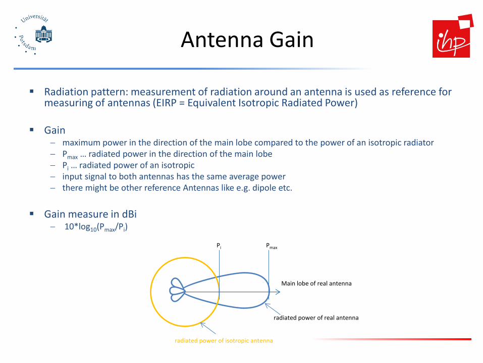
Radiation pattern: measurement of radiation around an antenna is used as reference for measuring of antennas (EIRP = Equivalent Isotropic Radiated Power)
Gain − maximum power in the direction of the main lobe compared to the power of an isotropic radiator − Pmax … radiated power in the direction of the main lobe − Pi … radiated power of an isotropic − input signal to both antennas has the same average power − there might be other reference Antennas like e.g. dipole etc.
Gain measure in dBi
− 10*log10(Pmax/Pi)
Main lobe of real antenna
Pmax Pi
radiated power of real antenna
radiated power of isotropic antenna

Modulation and Demodulation in the Radio
69
synchronization decision
digital data analog
demodulation
radio carrier
analog baseband signal
101101001 radio receiver
digital modulation
digital data analog
modulation
radio carrier
analog baseband signal
101101001 radio transmitter

Modulation Examples
Use data to modify the amplitude of a carrier frequency ! Amplitude Shift Keying
Use data to modify the frequency of a carrier frequency ! Frequency Shift Keying
Use data to modify the phase of a carrier frequency ! Phase Shift Keying ©
Tan
enba
um, C
ompu
ter N
etw
orks

Transmitted Signal vs. Received Signal
Wireless transmission distorts any transmitted signal Received signal is not the same as the transmitted signal Results in uncertainty at receiver about which bit sequence originally caused the transmitted signal Abstraction: Wireless channel describes these distortion effects Receiving power proportional to 1/d² (d = distance between sender and receiver) Receiving power additionally influenced by Fading (frequency dependent; H2O resonance at 2.5 GHz; O2 Resonance at 60 GHz) Attenuation (energy is distributed to larger areas with increasing distance) Shadowing Sources of distortion Reflection/Refraction – bounce of a surface; enter material Diffraction at edges – start “new wave” from a sharp edge Scattering at small obstacles – multiple reflections at rough surfaces Doppler fading – shift in frequencies (loss of center)
reflection scattering
diffraction
shadowing refraction

Attenuation results in Path Loss
Effect of attenuation Received signal strength is a function of the distance d between sender and transmitter Captured by Friis free-space equation d0 is far-field distance (d0 > 10 l), depends on antenna technology
− d0 ~ 1m for WLAN; d0 ~1 km for GSM Gt, Gr are antenna gains L ³ 1 summarizes losses through transmit/receive circuitry l is wavelength of carrier frequency
TX Antenne RX Antenne Ptx
Pr Pa
Precv
d Gt Gr
Precv based on Ptx
Precv based on measurement of Precv(d0) at d0

Application Examples
Signal has to have a minimum power at the receiver site (typical -80 to -90 dBm) − Estimation with Friis free-space equation
Effect on frequency − doubling the frequency reduces the received signal strength by a factor
of 4
Effect on distance − doubling the distance, requires 4 times the transmission power to have
the same receive power
2
recv 2 2 2 2 2P ( )(4 ) (4 )tx t r tx t rP G G P G Gd
d L d L fλ
π π⋅ ⋅ ⋅ ⋅ ⋅
= =⋅ ⋅ ⋅ ⋅ ⋅

Generalizing the Attenuation Formula and Other path-loss models
To take into account stronger attenuation than only caused by distance (e.g., walls, …), use a larger exponent γ > 2 − γ is the path-loss exponent
• In a room scenario the attenuation coefficient might be as high as 4 • In a town scenario even values of 5-6 are in use

Path loss in dB is defined as This results in:
Path Loss in Logarithmic form
𝑃𝑃𝑃𝑃 𝑑𝑑 ≔ 10 ∙ 𝑙𝑙𝑙𝑙𝑙𝑙𝑃𝑃𝑡𝑡𝑡𝑡
𝑃𝑃𝑟𝑟𝑟𝑟𝑟𝑟𝑟𝑟(𝑑𝑑) = 10𝑙𝑙𝑙𝑙𝑙𝑙𝑃𝑃𝑡𝑡𝑡𝑡 ∙ (4𝜋𝜋)² ∙ 𝑑𝑑0² ∙ 𝑃𝑃𝑃𝑃𝑡𝑡𝑡𝑡 ∙ 𝐺𝐺𝑡𝑡 ∙ 𝐺𝐺𝑟𝑟 ∙ 𝜆𝜆𝜆
∙𝑑𝑑𝑑𝑑0
𝛾𝛾

Link Budget Calculation
𝑃𝑃𝑟𝑟𝑟𝑟𝑟𝑟𝑟𝑟 𝑑𝑑 ≔ 10𝑙𝑙𝑙𝑙𝑙𝑙 𝑃𝑃𝑡𝑡𝑡𝑡∙𝐺𝐺𝑡𝑡∙𝐺𝐺𝑟𝑟∙𝜆𝜆𝜆 (4𝜋𝜋)²∙𝑟𝑟0²∙𝐿𝐿
∙ 𝑟𝑟0𝑟𝑟
𝛾𝛾 in dB
𝑃𝑃𝑟𝑟𝑟𝑟𝑟𝑟𝑟𝑟 𝑑𝑑 ≔ 10 log 𝑃𝑃𝑡𝑡𝑡𝑡 ∙ 𝐺𝐺𝑡𝑡 ∙ 𝐺𝐺𝑟𝑟 + 10𝑙𝑙𝑙𝑙𝑙𝑙𝜆𝜆2
4𝜋𝜋 2 ∙ 𝑑𝑑02 ∙ 𝑃𝑃+ 10𝑙𝑙𝑙𝑙𝑙𝑙
𝑑𝑑0𝑑𝑑
𝛾𝛾
path loss in dB until d0
Prcvd(d)= Ptx+Gt+Gr+PL in dB path loss in dB
until d
Assume Ptx = 30 dBm, Gt = Gr = 3 dBm
PL

Other path-loss models
The Friis formula is based on a physical propagation model Also possible: Statistical Models
− the path loss is no longer calculated per path but as a statistical function
Take obstacles into account by a random variation − Add a Gaussian random variable

Suitability of different frequencies – Attenuation
Attenuation depends on the used frequency Can result in a frequency-selective channel If bandwidth spans frequency
ranges with different attenuation properties
© http://w
ww
.itnu.de/radargrundlagen/grundlagen/gl24-de.html 𝑃𝑃𝑃𝑃 𝑑𝑑 ≔ 10 ∙ 𝑙𝑙𝑙𝑙𝑙𝑙
𝑃𝑃𝑡𝑡𝑡𝑡𝑃𝑃𝑟𝑟𝑟𝑟𝑟𝑟𝑟𝑟(𝑑𝑑)
= 10𝑙𝑙𝑙𝑙𝑙𝑙𝑃𝑃𝑡𝑡𝑡𝑡 ∙ (4𝜋𝜋)² ∙ 𝑑𝑑0² ∙ 𝑃𝑃𝑃𝑃𝑡𝑡𝑡𝑡 ∙ 𝐺𝐺𝑡𝑡 ∙ 𝐺𝐺𝑟𝑟 ∙ 𝜆𝜆𝜆
∙𝑑𝑑𝑑𝑑0
𝛾𝛾

Noise and interference
So far: only a single transmitter assumed Only disturbance: self-interference of a signal with multi-path “copies” of
itself In reality, two further disturbances Noise – due to effects in receiver electronics, depends on temperature
Interference from third parties
− Co-channel interference: another sender uses the same spectrum − Adjacent-channel interference: another sender uses some other part of the radio
spectrum, but receiver filters are not good enough to fully suppress it
Effect: Received signal is distorted by channel, corrupted by noise and interference

Signal propagation ranges
Transmission range communication possible low error rate Detection range detection of the signal
possible no communication
possible Interference range signal may not be
detected signal adds to the
background noise
80
distance
sender
transmission
detection
interference
Agenda
Microcontroller and Peripherals − Microarchitecture − Peripherals: GPIO, UART, SPI, I²C, ADC, DAC
Radio Modules Batteries, Memories, and Low-Power Issues
Memory
Microcontroller Sensor(s)/ actuator(s)
Communication device
Power supply
Power Consumption
Long life time is very often an issue in WSNs
Life time is affected by − Available energy in each node − power consumption of a mote
What affects the power consumption of a mote? − Microcontroller − Memory − Communication − (Sensors)

Agenda
Microcontroller Memories Radio Modules Motes and Low-Power Issues Batteries
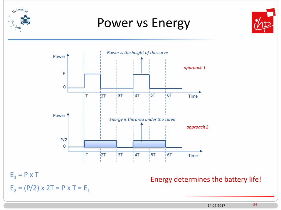
Power vs Energy
14.07.2017 84
E1 = P x T
E2 = (P/2) x 2T = P x T = E1 Energy determines the battery life!

Energy Consumption Examples (1)
Example: TI MSP430, fully operational consumes 1.2 mW @ 1 MHz Executes ~1 million instructions per second Energy per instruction: 0.0012Ws / 1.000.000 = 1.2 nJ per
instruction Batteries Small battery (“smart dust”): 1 J = 1 Ws Sufficient for executing 833 instructions
Processor cannot run all the time!
85

Energy Consumption Examples (2)
Energy consumption of various microcontroller Intel Desktop CPUs
− Core i7: 130 W − 386er: 2W
TI MSP 430 (@ 1 MHz, 3V): − Fully operation 1.2 mW − Deepest sleep mode 0.3 µW – only woken up by external interrupts (not even timer is running any more)
Atmel ATMega − Operational mode: 15 mW active, 6 mW idle − Sleep mode: 75 µW
Available energy using standard 2xAA batteries 2700 [email protected] = 6480 mWh
86
Processor Energy consumption Lifetime
Intel Core i7 130 W ~3 min
Intel 386 2 W ~3.2 hours
MSP430 (active) 0.0012 W 225 days
MSP430 (sleep) 0.0000003 W ~3400 years
ATMega (active) 0,015 W 18 days
ATMega (sleep) 0,000075 W ~10 years

Power Saving Modes in Microcontrollers
Idea If nothing to do, switch processor to power safe mode Typical modes for the controller Active, Idle, Sleep Strongly depends on hardware TI MSP 430, e.g.: four different sleep modes Atmel ATMega: six different modes Peripherals are even more important FW-Board with peripherals consumes
32 [email protected] = 105 mW >> 1.2 mW (power consumption microcontroller) Very often power consumption of the peripherals is much higher than that
of the microcontroller
87

Power Consumption in CMOS
CMOS Power = Dynamic Power + Static Power Dynamic Power power dissipation when logic gates are switching associated with active mode of operation consists of two
components: switching and internal power Static Power results from leakage currents dissipated also when transistors are turned off increases with device shrinking, i.e. technology scaling 88

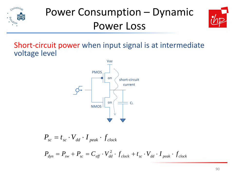
Power Consumption – Dynamic Power Loss
Switching Power – power consumption due to charge/discharge of load capacitance (CL)
89
2/ ddL VCTransitionEnergy ⋅=
clockddLsw fVCfTransitionEnergyP ⋅⋅⋅=⋅= α2/
α⋅= Leff CCclockddeffsw fVCP ⋅⋅= 2
Power Consumption – Dynamic Power Loss
Short-circuit power when input signal is at intermediate voltage level
90
clockpeakddscsc fIVtP ⋅⋅⋅=
clockpeakddscclockddeffscswdyn fIVtfVCPPP ⋅⋅⋅+⋅⋅=+= 2

Power Consumption - Static Power Loss
Static Power – Leakage power resulting from leaking currents in transistors I1 - reverse-bias p-n junction diode leakage I2 - subthreshold leakage I3 - gate leakage through the oxide I4 - gate induced drain leakage
91
𝑃𝑃𝑠𝑠𝑠𝑠𝑠𝑠𝑠𝑠 = 𝐼𝐼𝑙𝑙𝑙𝑙𝑙𝑙𝑙𝑙𝑙𝑙𝑙𝑙𝑙𝑙 ∙ 𝑉𝑉𝑟𝑟𝑟𝑟
𝐼𝐼𝑙𝑙𝑙𝑙𝑙𝑙𝑙𝑙𝑙𝑙𝑙𝑙𝑙𝑙 = 𝐼𝐼1 + 𝐼𝐼2 + 𝐼𝐼3 + 𝐼𝐼4

Standard Low-Power Approaches for Processors
Data Gating: Keep inputs of combinational logic blocks constantly either at 0 or 1
Clock Gating: Disable Clock
Power Gating: Disable power supply
Voltage and Frequency Scaling − Reduce power supply voltage and clock frequency
Standard Low Power Techniques – Multi-Vdd
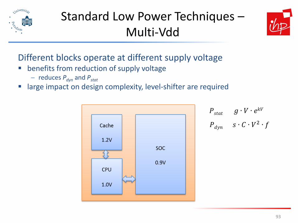
Different blocks operate at different supply voltage benefits from reduction of supply voltage
− reduces Pdyn and Pstat
large impact on design complexity, level-shifter are required
93
𝑃𝑃𝑑𝑑𝑑𝑑𝑑𝑑 = 𝑠𝑠 ∙ 𝐶𝐶 ∙ 𝑉𝑉2 ∙ 𝑓𝑓
𝑃𝑃𝑠𝑠𝑠𝑠𝑠𝑠𝑠𝑠 = 𝑙𝑙 ∙ 𝑉𝑉 ∙ 𝑒𝑒𝑘𝑘𝑉𝑉
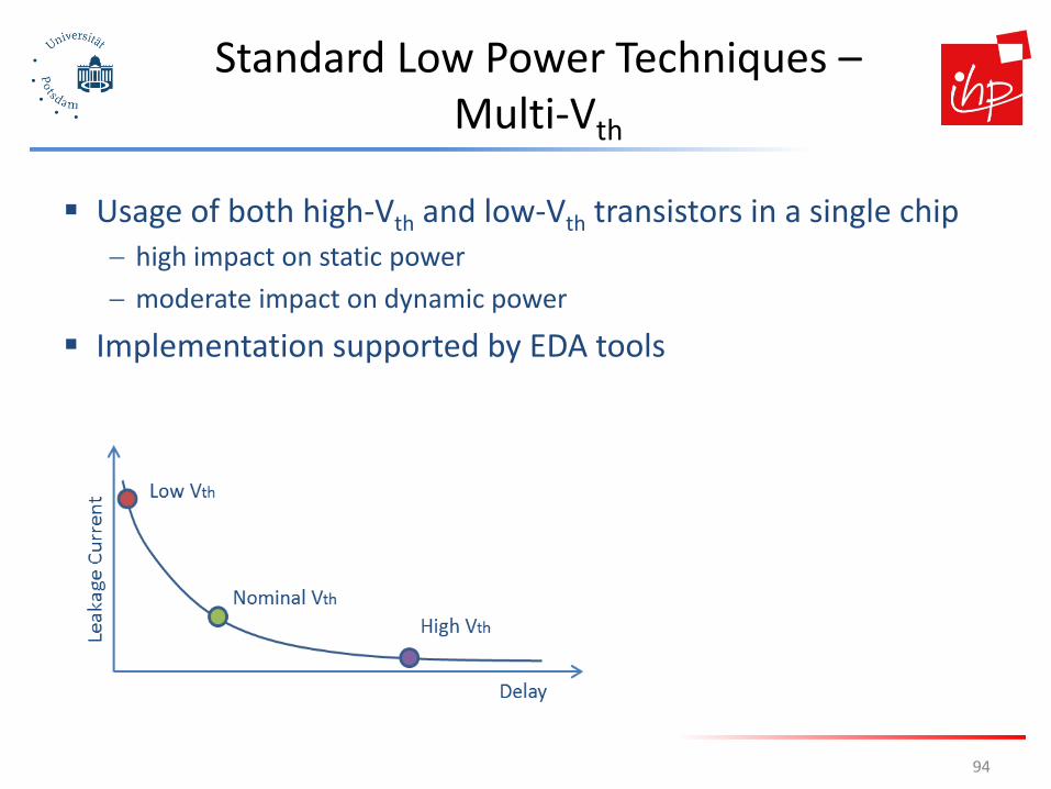
Standard Low Power Techniques – Multi-Vth
Usage of both high-Vth and low-Vth transistors in a single chip − high impact on static power − moderate impact on dynamic power
Implementation supported by EDA tools
94

Standard Low Power Techniques – Data Gating
Reduces switching activity in inactive data path blocks − reduces dynamic power consumption
Automatized implementation supported by modern EDA tools E.g., if processor is in idle state
− Fetching of instructions is avoided • also all memory operations are avoided
− Resumes to active mode with almost no delay
95

Standard Low Power Techniques – Clock Gating
Most popular standard technique Disabling the switching of clock nets in inactive parts of circuit
− significant reduction of switching power
Automatic clock gating insertion supported by EDA tools − Avoids switching in the circuitry − Only static power consumption remains (Pstat) − maybe also turn off the oscillators; then significant time is required for
enabling a stable clock
96
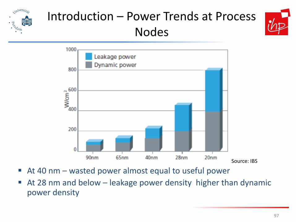
Introduction – Power Trends at Process Nodes
At 40 nm – wasted power almost equal to useful power At 28 nm and below – leakage power density higher than dynamic
power density
97
Source: IBS
Leakage Loss Vs Activity
0102030405060708090
100
20 10 1 0.1
Duty Cycle (%)
E sle
ep/E
tota
l (%
) Pdyn/Pstat=10000Pdyn/Pstat=5000Pdyn/Pstat=1000Pdyn/Pstat=500Pdyn/Pstat=100
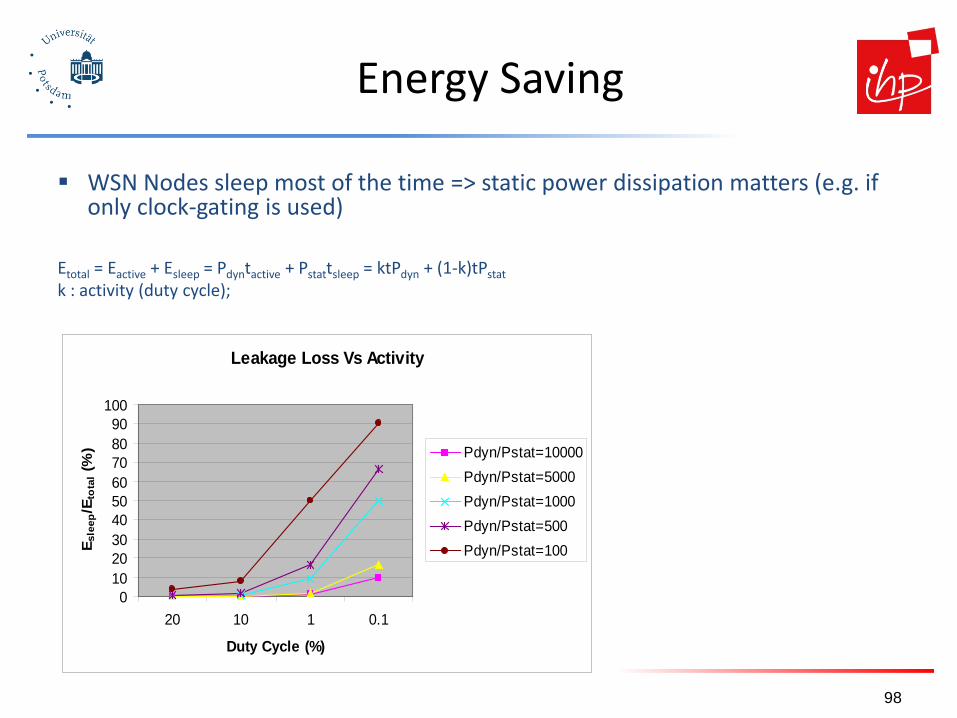
Energy Saving
WSN Nodes sleep most of the time => static power dissipation matters (e.g. if only clock-gating is used)
Etotal = Eactive + Esleep = Pdyntactive + Pstattsleep = ktPdyn + (1-k)tPstat k : activity (duty cycle);
98

Example

Advanced Low Power Techniques - Power Gating (1)
Shut down the power supply of inactive blocks − Avoids static (Pstat) and dynamic (Pdyn) power consumption
Significant overhead in time for bringing the processor back into active mode
Memory content may get lost − in some microcontrollers small parts of the memory can be powered in this
mode
100

Advanced Low Power Techniques – Power Gating (2)
Power gates – header vs footer Power gating controller – control of power-up sequences lsolation logic – prevents crowbar currents in active logic
blocks
101

Advanced Low Power Techniques – Power Gating (3)
Power Switches
102

Standard Low Power Techniques - Overview
Dynamic Power – multi-Vdd and clock gating most effective Static Power – multi-Vth and multi-Vdd most effective Implementation automated (except for multi-Vdd) Power Gating
− Switching modes complicated by uncertainty how long a sleep time is available − Alternative: Low supply voltage & clock
103
Technique Dynamic
Power Savings
Leakage Power Savings
Timing Penalty
Area Penalty
Impact: Architecture
Impact: Design
Impact: Verification
Impact: Place
&Route
Multi-Vth low
(<5%) 2-3x little little low low none low
Clock Gating medium (<30%) none little little low low none low
Multi-Vdd large
(<50%) 2x some little* high medium low medium
Operand Isolation
low (<5%) none little little low low none low
Gate-Level Techniques
low (<15%) none little little none none none none

Voltage and Frequency Scaling
Dynamic voltage scaling (DVS) Rationale: Power consumption P
depends on − Clock frequency − Square of supply voltage − P ~ f V²
Lower clock allows lower supply voltage
Easy to switch to higher clock
But: execution takes longer
104

Example Dynamic Voltage Scaling
Transmeta Crusoe processor: Scaling dynamics: 700 MHz @1.65 V to 200 MHz @1.1 V
− P@700MHz ~ 700*1.652 = 1905
− P@200MHz ~ 200*1.12 = 242
Power Consumption is reduced by factor P@700MHz/P@200MHz = 7.87
Speed reduction 700/200 = 3.5
Energy required per instruction is reduced by 3.5/7.875 = 0.44 − 44 % reduction
105

Advanced Low Power Design – Multi-Voltage Design
(a) SVS – static voltage scaling (b) MVS – multi-voltage scaling (c) DFVS – dynamic frequency and voltage scaling (d) AFVS – adaptive voltage scaling
106

Relation between Supply Voltage and Clock Frequency
Example for the MSP430
Question: When to throttle down? How to wake up again?
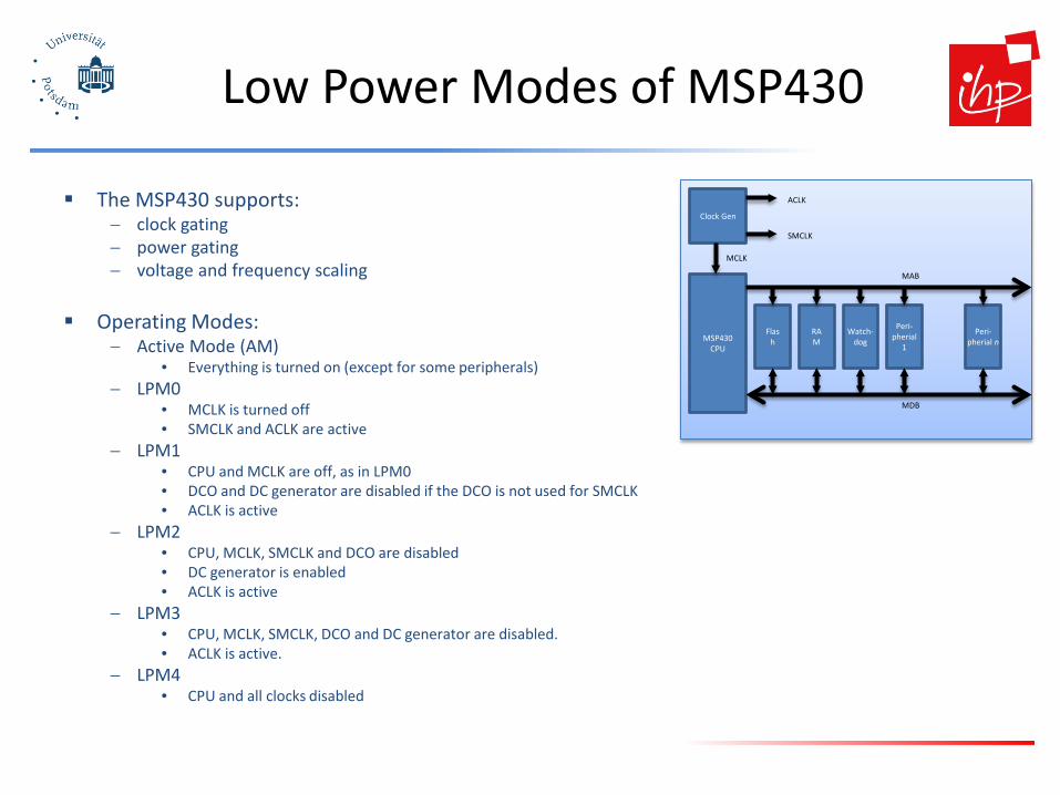
Low Power Modes of MSP430
The MSP430 supports: − clock gating − power gating − voltage and frequency scaling
Operating Modes:
− Active Mode (AM) • Everything is turned on (except for some peripherals)
− LPM0 • MCLK is turned off • SMCLK and ACLK are active
− LPM1 • CPU and MCLK are off, as in LPM0 • DCO and DC generator are disabled if the DCO is not used for SMCLK • ACLK is active
− LPM2 • CPU, MCLK, SMCLK and DCO are disabled • DC generator is enabled • ACLK is active
− LPM3 • CPU, MCLK, SMCLK, DCO and DC generator are disabled. • ACLK is active.
− LPM4 • CPU and all clocks disabled
Clock Gen
MSP430 CPU
MAB
MDB
Flash
RAM
Peri-pherial
1
Peri-pherial n
MCLK
ACLK
SMCLK
Watch- dog
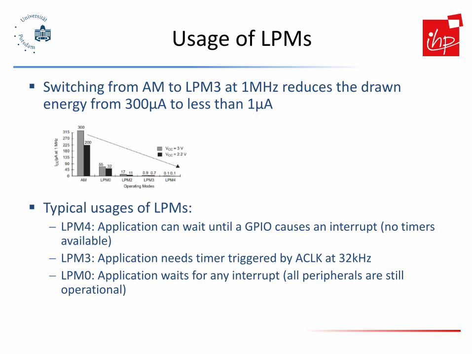
Usage of LPMs
Switching from AM to LPM3 at 1MHz reduces the drawn energy from 300µA to less than 1µA
Typical usages of LPMs: − LPM4: Application can wait until a GPIO causes an interrupt (no timers
available) − LPM3: Application needs timer triggered by ACLK at 32kHz − LPM0: Application waits for any interrupt (all peripherals are still
operational)

Controlling LPMs
SCG1 SCG0 OSCOFF CPUOFF Mode
0 0 0 0 AM
0 0 0 1 LPM0
0 1 0 1 LPM1
1 0 0 1 LPM2
1 1 0 1 LPM3
1 1 1 1 LPM4
1 1 1 1 LPM3.5 and LPM4.5
Reserved V SCG1 SCG0 OSCOFF CPUOFF GIE N Z C
0 1 2 3 4 5 6 7 8 9 15
LPMs are controlled with the status register (SR)

Entering and Exiting LPMs
An enabled interrupt event wakes the device from low-power operating modes LPM0 through LPM4
The program flow for exiting LPM0 through LPM4 is: − Enter interrupt service routine
• The PC and SR are stored on the stack. • The CPUOFF, SCG, and OSCOFF bits are automatically reset.
− Options for returning from the interrupt service routine
• The original SR is popped from the stack, restoring the previous operating mode.
• The SR bits stored on the stack can be modified within the interrupt service routine returning to a different operating mode when the RETI instruction is executed.

Examples at Assembler Level
Enter LPM0 Example BIS #GIE+CPUOFF,SR ; Enter LPM0 ; ... ; Program stops here ; ; Exit LPM0 Interrupt Service Routine BIC #CPUOFF,0(SP) ; Exit LPM0 on RETI RETI ; Enter LPM3 Example BIS #GIE+CPUOFF+SCG1+SCG0,SR ; Enter LPM3 ; ... ; Program stops here ; ; Exit LPM3 Interrupt Service Routine BIC #CPUOFF+SCG1+SCG0,0(SP) ; Exit LPM3 on RETI RETI ; Enter LPM4 Example BIS #GIE+CPUOFF+OSCOFF+SCG1+SCG0,SR ; Enter LPM4 ; ... ; Program stops here ; ; Exit LPM4 Interrupt Service Routine BIC #CPUOFF+OSCOFF+SCG1+SCG0,0(SP) ; Exit LPM4 on RETI RETI

Example for P1 interrupt
void main(void)
{
WDTCTL = WDTPW + WDTHOLD; // Stop watchdog timer
P1DIR |= 0x01; // Set P1.0 to output direction
P1IE |= 0x10; // P1.4 interrupt enabled
P1IES |= 0x10; // P1.4 Hi/lo edge
P1IFG &= ~0x10; // P1.4 IFG cleared
_BIS_SR(LPM4_bits + GIE); // Enter LPM4 w/interrupt
}
// Port 1 interrupt service routine
#pragma vector=PORT1_VECTOR
__interrupt void Port_1(void)
{
P1OUT ^= 0x01; // P1.0 = toggle
P1IFG &= ~0x10; // P1.4 IFG cleared
}

Agenda
Microcontroller Memories Radio Modules Motes and Low-Power Issues Batteries

Bulk-CMOS Trends
CMOS Scaling increases static power loss − static power loss of logic dominates static memory power loss
115
Bulk-CMOS

SOI-CMOS Power Trends
Static power consumption of memory dominates static power consumption of logic − power gating for memory?
116
Source: ITRS 2011
Silicon-on-Insulator (SOI)
Memory
Non-volatile memory (NVM) to store programs − PROM: For programs and fixed configuration data − EPROM: For programs and fixed configuration data − Flash: For programs and data − EEPROM: For programs and fixed configuration data − Power gating not critical: memory content does not get lost
RAM (VM): to store data and interim results
− SRAM common as data ram − Power gating critical: content gets lost; should we really turn it off
Benefit of Flash: reprogramming is possible in-the-field
117

Memory power consumption figures
FLASH writing/erasing is expensive (e.g. on Mica motes) Reading: 1.1 nAh per byte Writing: 83.3 nAh per byte
Comparing Flash and SRAM:
118
SRAM Flash
technology 250 nm 250 nm
read time 10 ns 10 ns
write time 10 ns 10 µs
read power 10 pJ 31 pJ
write power 10 pJ 80 nJ
endurance 1016 h 106 h

Non-volatile memory technologies for replacing SRAM
Solution with conventional memory architecture (SRAM + Flash) − store volatile data in flash before power-off − restore data in RAM after power-on
New memory technologies aim to have the advantage of
SRAM and NVM − high speed read time and fast write time − long endurance − low power consumption for read and write

STTRAM - Spin-Transfer Torque RAM
Each electron has a spin-property (small quantity of torque-momentum) − 50% of electrons have spin-up; 50% have spin-down
Spin-polarization is achieved by passing electrons through a magnetic layer
Memory element: Two ferromagnetic layers are isolated with a tunnel barrier layer. Fixed layer is used for polarization Free layer can be programmed
− If both layer have the same magnetization the resistance is low (logic “1”) or the alignment is anti-parallel which results in a high resistance (logic “0”).
Source: A13ean - Own work, CC BY-SA 3.0, https://commons.wikimedia.org/w/index.php?curid=16209514
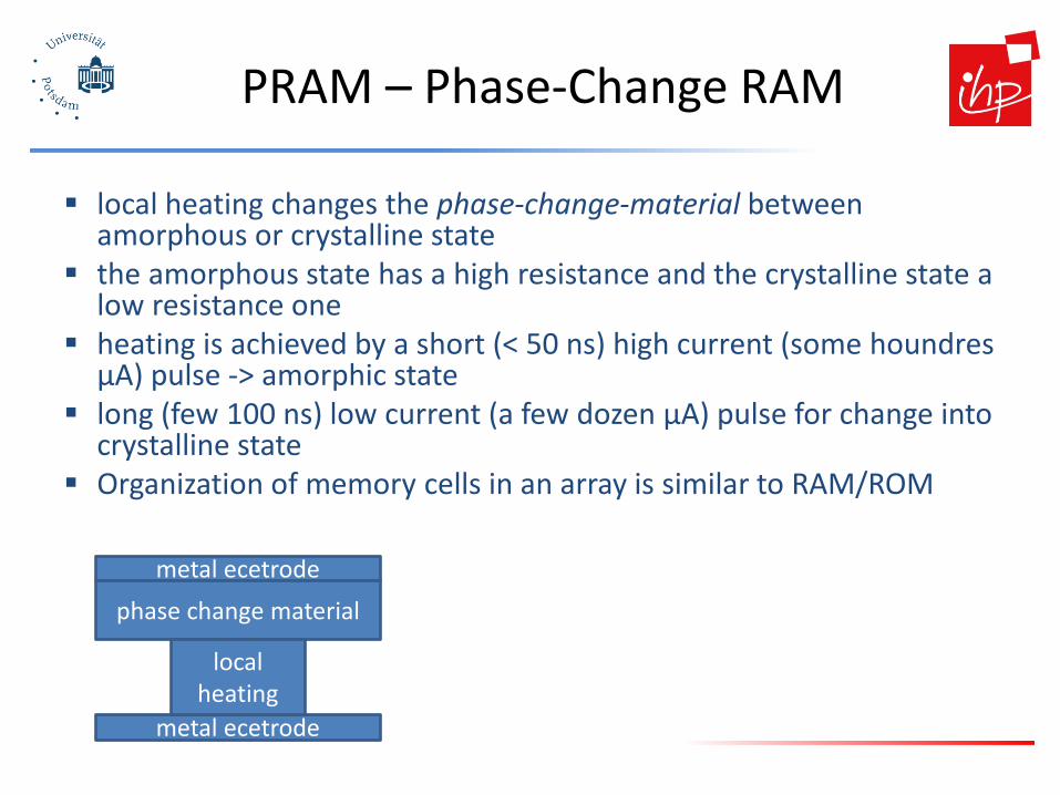
PRAM – Phase-Change RAM
local heating changes the phase-change-material between amorphous or crystalline state
the amorphous state has a high resistance and the crystalline state a low resistance one
heating is achieved by a short (< 50 ns) high current (some houndres µA) pulse -> amorphic state
long (few 100 ns) low current (a few dozen µA) pulse for change into crystalline state
Organization of memory cells in an array is similar to RAM/ROM
metal ecetrode
metal ecetrode
phase change material
local heating

RRAM – Resistive RAM
Resistance of a Metal-Insulator-Metal stack can be changed electrically
Applying a specific current the resistance of the memristor is switched from high to low and vice versa.
Source: Implications of the Incremental Pulse and Verify Algorithm on the Forming and Switching Distributions in RERAM Arrays

FRAM – Ferroelectric RAM
A ferroelectric material has an electrical polarization Structure of a memory cell is similar to a flash cell
− ferroelectric material is used as a “floating-gate” write-operation:
− Polarization is set by applying a voltage from source to gate read-operation:
− Applying voltage from source to drain − measuring the current
E.g. Bariumtitanat

Comparison of different NVM technologies
SRAM Flash MRAM RRAM FRAM
Technology 250 nm 250 nm 90 nm 250nm 130 nm
read time 10 ns 10 ns 5 ns 40 ns 384 ns
write time 10 ns 10 µs 4 ns 60 ns 320 ns
read power 10 pJ 31 pJ 0.3 pJ 31 pJ 0.66 pJ
write power 10 pJ 80 nJ 6 pJ 2 pJ 2.2 pJ
endurance cycles
1016 106 inf. 107 1014

Agenda
Microcontroller Memories Radio Modules Motes and Low-Power Issues Batteries

Transceiver states
Transceivers can be put into different operational states, typically: Transmit: Sending data
Receive: Receiving data
Idle: Ready to receive, but not doing so (listening to the channel)
− Some functions in hardware can be switched off, reducing energy consumption a little
− Leakage is a main source of power dissipation
Sleep – significant parts of the transceiver are switched off − Not able to immediately receive something − Recovery time and startup energy to leave sleep state can be significant
126

127
CC1101

WiFi vs WSN
Comparing WiFi transceivers and WSN transceivers (similar to Desktop CPUs and µC) WiFi Up to 54 MBit/s; for WSN: < 250 kbit/sec) Relatively long distance (100s of meters possible); for WSN: < 100m expensive and power hungry
128
0.01 mA0.8 mASleep
21 mA170 mARx
20 mA170 mATx
CC2420OWLAN211g
assumed, since rx energy not in datasheet
Transceivers WiFi vs WSN:

Transmitter power/energy consumption for n bits
Power consumption is composed of RF signal generation (amplifier power Pamp) Power consumption of the electronic components in the transceiver (PtxElec) Amplifier power: Pamp = αamp + βamp × Ptx Ptx radiated power αamp, βamp constants depending on amplifier architecture
Example
− αamp = 174 mW, βamp = 5
Highest efficiency ηPA at maximum output power − Typical efficiency figures range between 15% and 70%
129
174 5tx tx
PAamp tx
P PP P
η = =+ ⋅
Ptx in dBm Ptx in mW nPA in %
0 1 0,55 1 1,3 0,69 5 3,2 1,66
10 10 4,46 20 100 14,83 27 501,2 18,70 30 1000 19,32

Transmitter power/energy consumption for n bits
Time to transmit n bits: n / (R × Rcode) R nomial data rate (e.g. 10kb/s) Rcode coding rate (e.g. ¾) R × Rcode is the effective data rate (i.e., data rate for data bits) Number of sent bits: n / Rcode
− e.g.: 1000/(3/4) = 4000/3 =1300 To leave sleep mode Time Tstart average power Pstart
Etx = Tstart × Pstart + (n / (R × Rcode) × (PtxElec + Pamp))
130
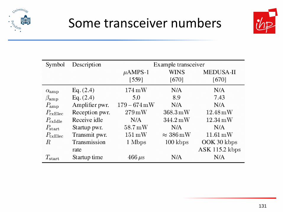
Some transceiver numbers
131
Receiver power/energy consumption for n bits
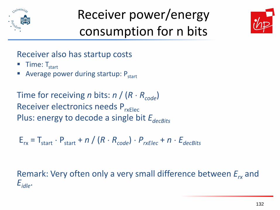
Receiver also has startup costs Time: Tstart Average power during startup: Pstart
Time for receiving n bits: n / (R × Rcode) Receiver electronics needs PrxElec Plus: energy to decode a single bit EdecBits Erx = Tstart × Pstart + n / (R × Rcode) × PrxElec + n × EdecBits Remark: Very often only a very small difference between Erx and Eidle.
132

Controlling transceivers
Low duty cycle techniques (similar to µC)
Easy to apply for transmitter, because the µC can turn on the transmitter on demand − But: When is it worthwhile to switch off?
Difficult for receiver
− If turned off, then no reception is possible − Strong dependence between protocols and power consumption of the
receiver − Elegant solution: Wakeup Receiver
133
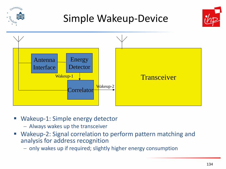
Simple Wakeup-Device
Wakeup-1: Simple energy detector − Always wakes up the transceiver
Wakeup-2: Signal correlation to perform pattern matching and analysis for address recognition − only wakes up if required; slightly higher energy consumption
134
Antenna Interface
Energy Detector
Correlator
Transceiver Wakeup-1
Wakeup-2

Agenda
Microcontroller Memories Radio Modules Motes and Low-Power Issues Batteries

Mote Power Consumption
Depends on the power consumption of its components Microcontroller should control the state of the peripherals Radio Module (Transceiver/Receiver on/off/idle) Sensors (on/off) Memories (on/off) µC (active/idle/sleep)
Deeper sleep-mode refers to lower energy consumption In general: Switching between these states takes time consumes power only beneficial, if power can be saved

Switching between modes
Simplest idea: Greedily switch to lower mode whenever possible MCU low power modes Radio sleep / idle states Sensors powered down
137
Pactive
Psleep
time tevent t1
Esaved Eoverhead
τdown τup
Esaved = (tevent-t1) × Pactive - tdown(Pactive + Psleep)/2 - (tevent-t1-tdown) × Psleep
Eoverhead =tup(Pactive + Psleep)/2

Switching between modes
Pays off if Esaved > Eoverhead
138
Pactive
Psleep
time tevent t1
Esaved Eoverhead
τdown τup
Esaved = (tevent-t1) × Pactive - tdown(Pactive + Psleep)/2 - (tevent-t1-tdown) × Psleep
Eoverhead =tup(Pactive + Psleep)/2
112
active sleepevent down up
active sleep
P Pt t
P Pτ τ +
− > + ⋅ −

Computation vs. communication
Tradeoff Directly comparing computation/communication energy cost
not possible Energy ratio of “sending one bit” vs. “computing one
instruction”: Anything between 220 and 2900 in the literature − Computing a single instruction: 1 nJ − TX single bit with Bluetooth: 100 nJ (w/o startup costs, etc.) − TX single bit with RFM TR100: 1000 nJ
Communication is significantly more energy consuming than computing
Local processing of data pays off, if reduction of 1 bit in data is achieved with less than 1000 executed instructions
139

Computation vs. communication
Key technique in WSN – in-network processing! Exploit compression schemes, intelligent coding schemes, … Process data in the nodes and only send information rather than
data Do as much as possible at the edges of the network
140
22°C 43°C
22°C
21°C
21.7°C

Agenda
Microcontroller and Peripherals Memories Radio Modules Motes and Low-Power Issues Batteries
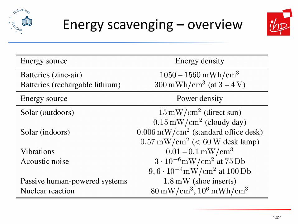
Energy scavenging – overview
142

Battery examples
Motes needs high-capacity, small, light and low-price batteries Preferred are batteries with high energy per volume rates: Thus, primary batteries often preferred However, other metrics must be considered as well: Zinc-air batteries have attractive energy density, but very short lifetime (in
the order of weeks) due to self-discharge
Primary batteries
Chemistry Zinc-air Lithium Alkaline Energy (J/cm3) 3780 2880 1200
Secondary batteries
Chemistry Lithium NiMHd NiCd Energy (J/cm3) 1080 860 650
143

Battery examples
Problem with batteries: Reduction of battery’s voltage as the capacity drops Example: Tmote Sky needs voltage > 2.1 V, and > 2.7 V for programming 2x AA eneloops: >90% of capacity @ > 2.1V
144

Battery examples
Self-discharge problem Tmote sky with 2xAA and schedule-based MAC (DLDC-MAC) Beacon period: 1 minute Beacon length: 128 bytes (4.1 ms) Beacon rx time: 11 ms
(clock drift compensated) Number of neigbours: 4
145
Sleep mode 0.24 mAh / day
Beacons (tx, rx) 0.49 mAh / day
Self discharge 0.82 mAh / daytotal: 1.55 mAh / day
Lifetime: more than 3 years
Self discharge is the major „energy consumer”

Summary
Communication is significantly more energy consuming than computing − in-network processing
Main solution to save energy:
− If nothing to do, use power safe mode • many options for µC, from power gating, clock-gating to DVS
− Turn off peripherals, in particular radio modules
• Low duty cycle required to achieve reasonable lifetimes • huge impact on the design of communication protocols
146