what is an “soc”? soc = soc = system on chip = system on a chip wider use: a chip that...
TRANSCRIPT

What is an “SoC”?
• SoC = SOC = System on Chip = System on a Chip• Wider use:
a Chip that implements a Complete System• More common use:
a Chip withone or more CPU cores,Peripheral Interface Blocks,and Dedicated HW Blocksaround a System Bus

What is ASIC, FPGA, SoC?
ASAASASIC
ASAASFPGA
ASAASSoC

Full-custom ASIC Gate-array(Structured ASIC)
FPGA
LayoutNot Pre-designed
Whole ChipPre-designed
Individual Gates and MemoryPre-designed
All Layout except WiresPre-designed
SoC

Inside an FPGA
CLB: Configurable Logic Block
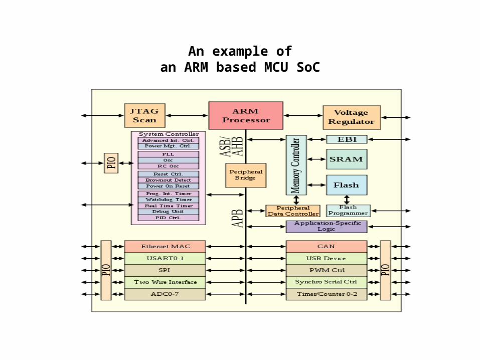
An example ofan ARM based MCU SoC

From a Designer’s Perspective
• ASIC, FPGA, SoC: all the same from a designer’s point of view
• We are in the SoC age =>
• Shop for IP blocks(IP block = Library block)
• Integrate them with each other and your design

What is ASIC?• IC
• Full-custom IC
• IC = SP or ASSP• SP = Standard Product
= Memory chip, Processor• ASSP = Application Specific Standard Product
= USB interface chip for ex.
• ASIC =>Think of Vestel or Cisco – an equipment=box=system makerthat buys ICs (SP or ASSP) puts them on a PCB.They sometimes need extra logic =>
hence ASIC (Application Specific Integrated Circuit)

Contemporary (wider)meaning of ASIC
• Previous slide described the original (narrow) meaning of ASIC(how the word ASIC came about)
• Such chips required quick methods for design because:• constraints in design time• constraints in design personnel• designs were not so aggressive
• This resulted in what we call: ASIC Design Flow
• Hence: an “ASIC Designer” doing “ASIC Design”may be working on an SPdone in ASIC Design Flowas opposed to Full-Custom Flow.

Why/when design your own chipor customize an SoC?
As opposed to taking a CPU and writing code that runs on it
BECAUSE:
• CPU solution is not fast enough(FPGA is slower but offers more parallelism)
• CPU is too expensive• CPU sucks too much power• CPU cannot meet the exact I/O timing requirements (no later no earlier)• CPU does not have the right number and mix of I/O pins• Form-factor: CPU is too big and/or requires a heat/sink, fan, and/or chip-set

a LOOK at the SECTOR

1. Intel (USA): $50B2. Samsung (Korea): $29B/$260B+
3. TSMC (Taiwan): $15B4. TI (USA): $14B5. Toshiba (Japan): $13B/$80B
6. Renesas (Japan): $11B7. Qualcomm (USA): $10B8. STMicro (Fr-Ita): $10B9. Hynix (Korea): $9B10. Micron (USA): $7B
11. Broadcom (USA): $7B12. AMD (USA): $6B13. Infineon (Germany): $5B14. Sony (Japan): $5B/$90B
15. Freescale (USA): $4B16. Elpida (Japan): $4B17. NXP (Holland): $4B18. UMC (Taiwan): $4B19. NVIDIA (USA): $4B20. Globalfoundries (USA): $4B
FPGA market size $5BFab = Foundry
Fabless semi
Top Semi Companies (2011)
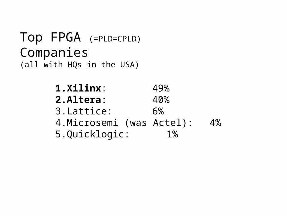
1. Xilinx: 49%2. Altera: 40%3. Lattice: 6%4. Microsemi (was Actel): 4%5. Quicklogic: 1%
Top FPGA (=PLD=CPLD) Companies(all with HQs in the USA)

DESIGN ISSUES

ASIC Implementation Flow
ASIC Design
Fabrication
Package/Test
Validation
3-12 months
~ 2 months
~ 1 month
~ 1 month
NRE = $100K - $4M
SW tools = $100K - $1M
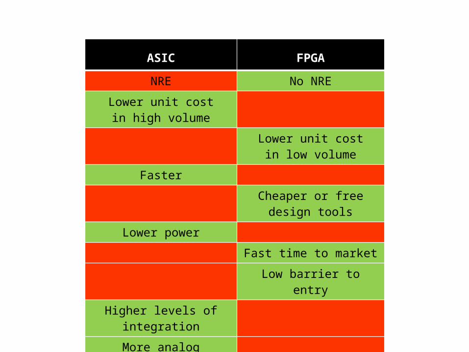
ASIC FPGA
NRE No NRE
Lower unit costin high volume
Lower unit costin low volume
FasterCheaper or free design tools
Lower power
Fast time to market
Low barrier to entryHigher levels of integration
More analog integrationProgrammable

- Next few slides are Courtesy of Xilinx (DAC 2001)


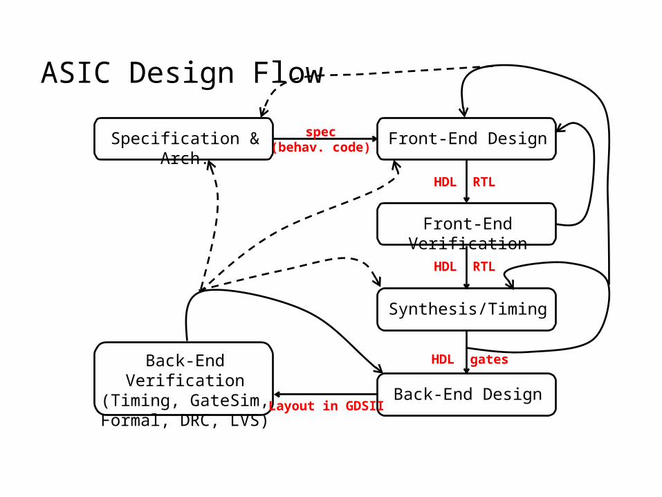
ASIC Design Flow
Front-End Design
Front-End Verification
Specification & Arch.
Back-End Verification(Timing, GateSim,Formal, DRC, LVS) Back-End Design
Synthesis/Timing
spec(behav. code)
HDL RTL
HDL RTL
HDL gates
Layout in GDSII

ASIC Design Tool-set
Front-End Design
Front-End Verification
Back-End Verification(Timing, GateSim,Formal, DRC, LVS) Back-End Design
Synthesis/Timing
Layout in GDSII
Editor
Simulator SW
HDL RTL
HDL RTL
HDL gates
Synthesis SW
Physical design, verif., DFT/ATPG SWs
Stdcell Library

1. Synopsys: $1500M2. Mentor Graphics: $900M3. Cadence: $850M4. Other: 27%
(Above are my 2010 estimates.Total market size: $4.5B)
Top EDA Companies(all with HQs in the USA)

FPGA Design Flow
Front-End Design
Front-End Verification
Specification & Arch.
Back-End Verification(Timing, GateSim,Formal, DRC, LVS)
Synthesis,Back-end,
Timing
spec(behav. code)
Bitfile
HDL RTL
HDL RTL

FPGA DesignTool-set for Xilinx
Front-End Design
Front-End Verification
Synthesis,Back-end,
Timing
Bitfile
HDL RTL
HDL RTL
Xilin
x IS
EEd
itor,
Sim
ulat
or, S
ynth
esis
All i
n on
e ID
E

MODERN DIGITAL DESIGN- BASICS -

You hardly need anything you learned in your Logic coursein Modern (HDL and Synthesis based) Digital Designbecause:
• We write code• We don’t design circuits• At least no gate-level circuits
• We don’t care about theorems in Boolean Algebra • We don’t care about Karnaugh-maps
• The synthesis SW (compiler)does the logic minimization for us
• The FPGA has 1000s of gates anyway• (OK, in some extreme cases we may need to care)
• Before we care about area minimizationwe need to care about meeting timing

We write RTL code

What is RTL code?

What is the RTL programming paradigm?

What does RTL mean in the first place?
RTL = RT-Level = Register Transfer Level

What is RT-Level digital (logic) design?
Cloud of Logic(Combinational)
Flop
more Flops
Inputs
Outputs
Your (RTL) code describes the logic cloud
storedVars
storedVars_next
Everything is a STATE MACHINE!

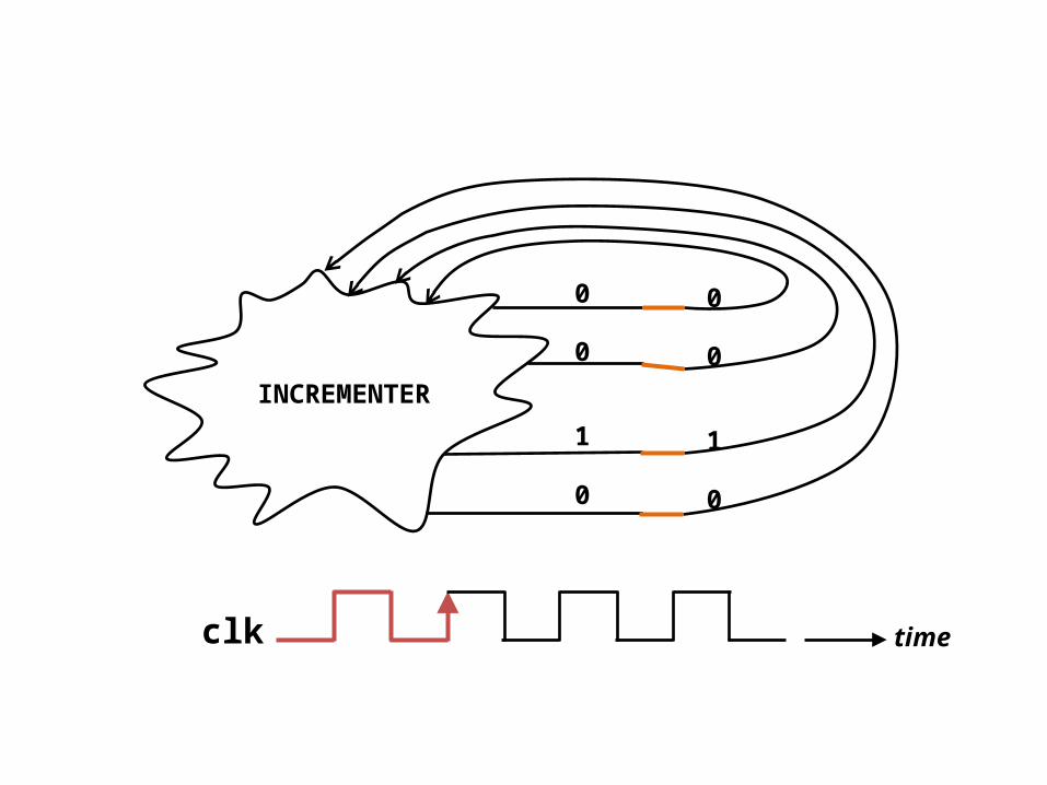
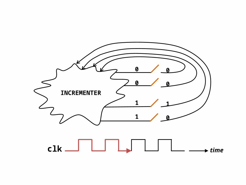
for ex. INCREMENTER
clk
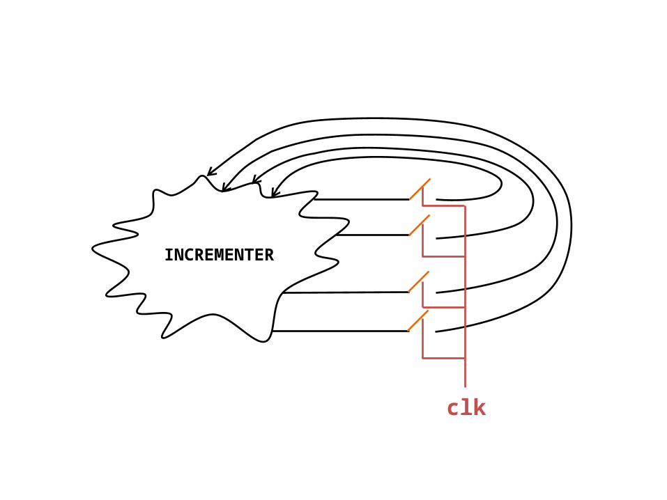
INCREMENTER
clk

INCREMENTER
0
0
0
0
0
0
0
1
clk time

INCREMENTER
0
0
0
1
0
0
0
1
clk time

INCREMENTER
0
0
0
1
0
0
1
0
clk time
INCREMENTER
0
0
1
0
0
0
1
0
clk time
INCREMENTER
0
0
1
0
0
0
1
1
clk time

INCREMENTER
0
0
1
1
0
0
1
1
clk time
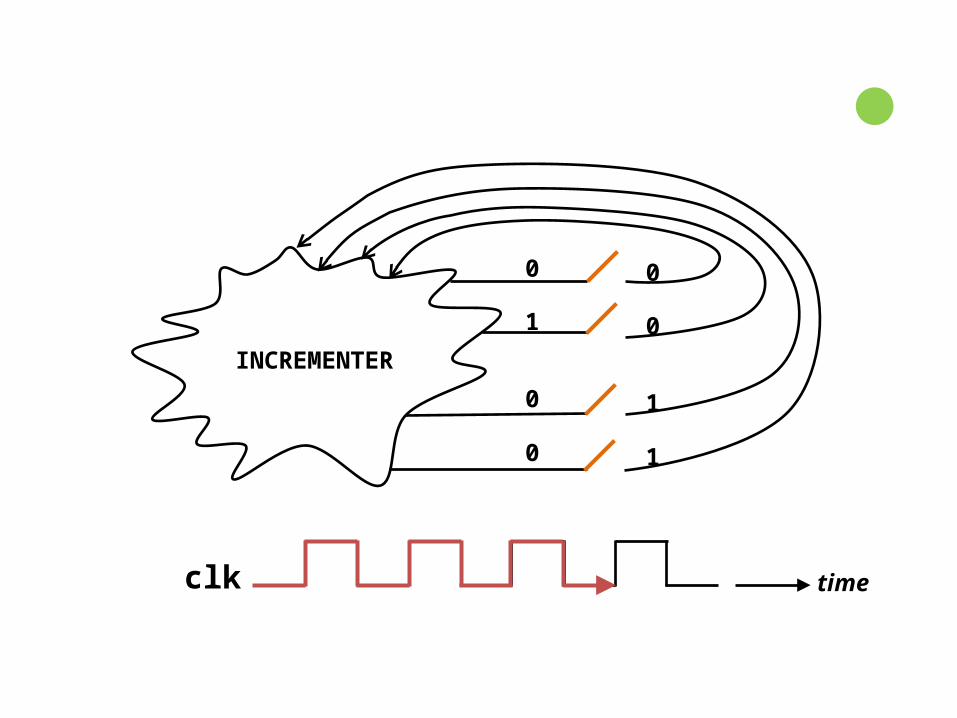
INCREMENTER
0
0
1
1
0
1
0
0
clk time

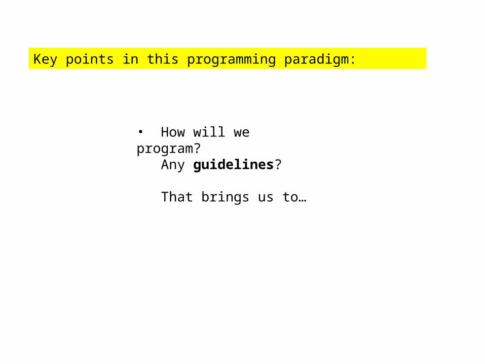
Key points in this programming paradigm:
• What are we programming?
• How will we program?(Any guidelines?)
• What is a “flop” by the way?
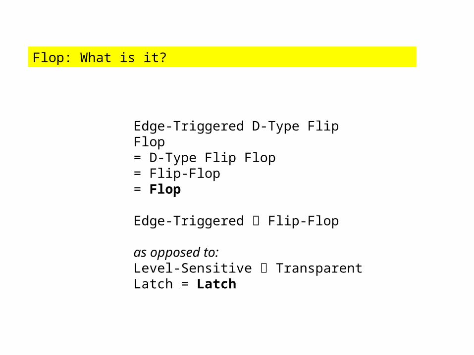
Flop: What is it?
Edge-Triggered D-Type Flip Flop= D-Type Flip Flop= Flip-Flop= Flop
Edge-Triggered Flip-Flop
as opposed to:Level-Sensitive Transparent Latch = Latch

Flop: explained with WAVEFORMS
clk
D Q
clk
D
Qpo
sedg
e
pose
dge
pose
dge
pose
dge
Flop = 1-bit DigiCam

2 Flops back to back = Shift Register
clk
D
clk
D
Q1
Q2Q1
Q2

How a FLOP behaves (shown with a SHIFT REGISTER)
1 0 0 1 1
1 0 1
flop1 flop2
t = before posedge clk

How a FLOP behaves (shown with a SHIFT REGISTER)
1 0 1
1 1 0 0 1flop1 flop2
t = posedge clk
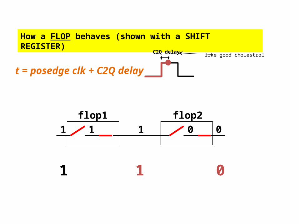
How a FLOP behaves (shown with a SHIFT REGISTER)
1 1 0
1 1 1 0 0flop1 flop2
t = posedge clk + C2Q delay
C2Q delay like good cholestrol
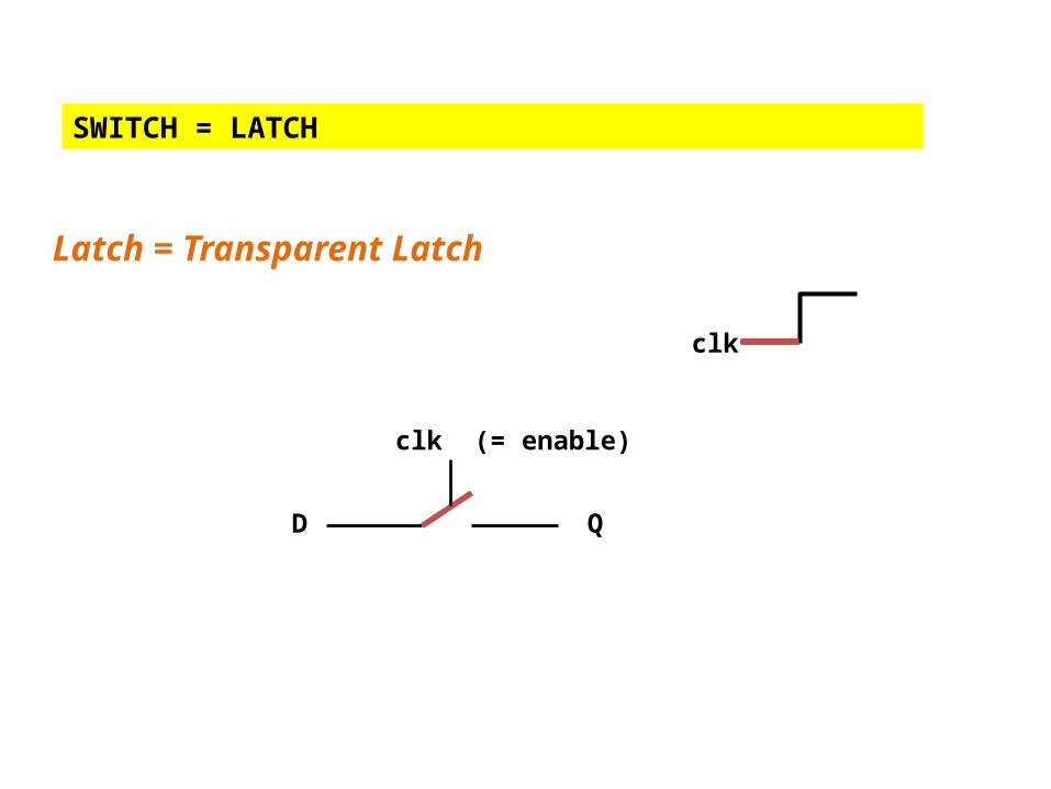
SWITCH = LATCH
Latch = Transparent Latch
D Q
clk
clk (= enable)

SWITCH = LATCH
Latch = Transparent Latch
D Q
clk (= enable)
clk

SWITCH = LATCH
Latch = Transparent Latch
DQ
clk (= enable)
1
0

FLOP = 2 back-to-back LATCHes
flop
latch (master) latch (slave)
clk
clk1 clk2
clkclk1clk2
ClockToQ (C2Q) delay
C2Q
del
ay
NON-OVERLAPPING

Key points in this programming paradigm:
• What are we programming?
Your programDESCRIBES
this
clk

Key points in this programming paradigm:
• What are we programming?
Your programDESCRIBES
ONE CYCLE
clk
Key points in this programming paradigm:
• How will we program?Any guidelines?
That brings us to…

VERILOG TUTORIAL- BASICS -

example design: counter
counter
module counter(); endmodule

example design: counter
counter
module counter( cnt); output [3:0] cnt; endmodule
4cnt

example design: counter
counter
module counter( cnt, btn); output [3:0] cnt; input btn; endmodule
1btn
4cnt

example design: counter
counter
module counter(cnt, btn, clk); output [3:0] cnt; input btn, clk; endmodule1
btn4
cnt
clk

example design: counter
module counter(cnt, btn, clk); output [3:0] cnt; input btn, clk;
endmodule1btn
4cnt
clk
4
cntNxt
always @(*)

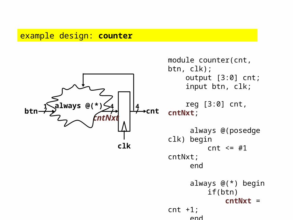
example design: counter
module counter(cnt, btn, clk); output [3:0] cnt; input btn, clk;
reg [3:0] cnt, cntNxt;
always @(posedge clk) begin cnt <= #1 cntNxt; end endmodule
1btn
4cnt
clk
4
cntNxt
example design: counter
module counter(cnt, btn, clk); output [3:0] cnt; input btn, clk;
reg [3:0] cnt, cntNxt;
always @(posedge clk) begin cnt <= #1 cntNxt; end always @(*) begin if(btn) cntNxt = cnt +1; end endmodule
1btn
4cnt
clk
4
cntNxt
always @(*)

example design: counter
module counter(cnt, btn, clk); output [3:0] cnt; input btn, clk;
reg [3:0] cnt, cntNxt;
always @(posedge clk) begin cnt <= #1 cntNxt; end always @(*) begin if(btn) cntNxt = cnt +1; end endmodule
btn
4cnt
clk
4
+1 1
0

example design: counter
module counter(cnt, btn, clk); output [3:0] cnt; input btn, clk;
reg [3:0] cnt, cntNxt;
always @(posedge clk) begin cnt <= #1 cntNxt; end always @(*) begin cntNxt = cnt; if(btn) cntNxt = cnt +1; end endmodule
btn
4cnt
clk
4
+1 1
0

example design: counter
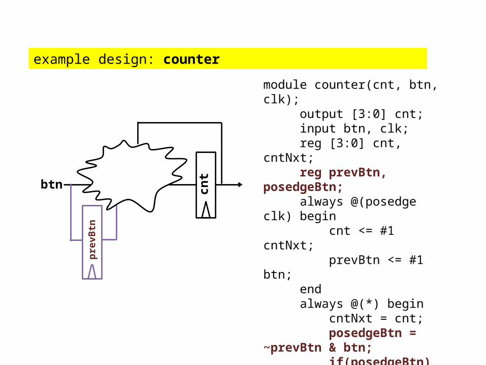
module counter(cnt, btn, clk); output [3:0] cnt; input btn, clk; reg [3:0] cnt, cntNxt; reg prevBtn, posedgeBtn; always @(posedge clk) begin cnt <= #1 cntNxt; prevBtn <= #1 btn; end always @(*) begin cntNxt = cnt; posedgeBtn = ~prevBtn & btn; if(posedgeBtn) cntNxt = cnt +1; endendmodule
btn cnt
pre
vBtn

example design: counter
module counter(cnt, btn, clk); output [3:0] cnt; input btn, clk; reg [3:0] cnt, cntNxt; reg prevBtn; always @(posedge clk) begin cnt <= #1 cntNxt; prevBtn <= #1 btn; end always @(*) begin cntNxt = cnt; if(~prevBtn & btn) cntNxt = cnt +1; endendmodule
btn cnt
pre
vBtn

example design: counter
module counter(cnt, btn, clk); output [3:0] cnt; input btn, clk; reg [3:0] cnt, cntNxt; reg prevBtn; wire posedgeBtn; always @(posedge clk) begin cnt <= #1 cntNxt; prevBtn <= #1 btn; end assign posedgeBtn = ~prevBtn & btn; always @(*) begin cntNxt = cnt; if(posedgeBtn) cntNxt = cnt +1; endendmodule
btn cnt
pre
vBtn
assign
always @(*)

example design: counter
module counter(cnt, btn, clk); output [3:0] cnt; input btn, clk; reg [3:0] cnt, cntNxt; reg prevBtn; wire posedgeBtn; always @(posedge clk) begin cnt <= #1 cntNxt; end posDet posDet(clk, btn, posedgeBtn); always @(*) begin cntNxt = cnt; if(posedgeBtn) cntNxt = cnt +1; endendmodule
btn
cnt
posDet
clk

example design: counter
module counter(cnt, btn, clk); output [3:0] cnt; input btn, clk; reg [3:0] cnt, cntNxt; reg prevBtn; wire posedgeBtn; always @(posedge clk) begin cnt <= #1 cntNxt; prevBtn <= #1 btn; end assign posedgeBtn = ~prevBtn & btn; always @(*) begin cntNxt = cnt; if(posedgeBtn) cntNxt = cnt +1; endendmodule
btn cnt
pre
vBtn
assign
always @(*)

example design: counter
btn cnt
pre
vBtn
assign
always @(*)
module counter(cnt, btn, clk); output [3:0] cnt; input btn, clk; reg [3:0] cnt, cntNxt; reg prevBtn; wire posedgeBtn; always @(posedge clk) begin cnt <= #1 cntNxt; prevBtn <= #1 btn; end always @(*) posedgeBtn = ~prevBtn & btn; always @(*) begin cntNxt = cnt; if(posedgeBtn) cntNxt = cnt +1; endendmodule
example design: counter
module counter(cnt, btn, clk); output [3:0] cnt; input btn, clk; reg [3:0] cnt, cntNxt; reg prevBtn, posedgeBtn; always @(posedge clk) begin cnt <= #1 cntNxt; prevBtn <= #1 btn; end always @(*) begin cntNxt = cnt; posedgeBtn = ~prevBtn & btn; if(posedgeBtn) cntNxt = cnt +1; endendmodule
btn cnt
pre
vBtn

Expressing ALGORITHMs in RT-Level paradigm?
1. Think of your HW module as a netlist of HW submodules.
2. Each submodule can in turn be a netlist of subsubmodules.
3. Leaf modules can be expressed by behavior that can be synthesized: (what we call) RTL code.
4. RTL is how we express an algorithm in HW.
5. Break your algorithm into clock cycles.
6. You have to specify what is done in each cycle.

Expressing ALGORITHMs in RT-Level paradigm? – cont’d
6. Think of it as a STATE MACHINE where every state is executed in a different cycle.
7. Store everything that needs top be remembered between states (= cycles) in explicitly coded REGISTERs.
8. Store also the STATE in an explicitly coded register.
9. At the top of the put a case(STATE).
10. What you will really code other than the registers is actually a Truth Table coded with a high-level language.
11. That is: Outputs depend on only inputs, which are external inputs plus register outputs.

GOLDEN RULES L

GOLDEN RULE 1
NO COMBINATIONAL LOOP
always @(*)

GOLDEN RULE 1
NO COMBINATIONAL LOOP
always @(*)
always @(*) begin if(cntNxt) cntNxt = cnt –1;end
cntNxt

GOLDEN RULE 1
NO COMBINATIONAL LOOP
always @(*)
always @(*) begin if(cnt) cntNxt = cnt –1;end

GOLDEN RULE 1
NO COMBINATIONAL LOOP
always @(*)
always @(*) begin if(cnt) cntNxt = cnt –1; else cntNxt = cntNxt;end

GOLDEN RULE 1
NO COMBINATIONAL LOOP
always @(*)
always @(*) begin if(cnt) cntNxt = cnt –1; else cntNxt = cnt;end

GOLDEN RULE 1 – IMPLICATION
Always have DEFAULT ASSIGNMENTSat the top of always @(*)
always @(*) begin cntNxt = cnt; if(cnt) cntNxt = cnt –1;end

GOLDEN RULE 1 – IMPLICATION
Always have DEFAULT ASSIGNMENTSat the top of always @(*)
always @(*) begin cntNxt = cnt; if(cntNxt) cntNxt = cnt –1;end

GOLDEN RULE 2
NO INDIRECT COMBINATIONAL LOOPS
always @(*) always @(*)
always @(*) and assign are equivalent

GOLDEN RULE 3
NO MULTIPLE DRIVERS
always @(*)
always @(*)
sameVar
sameVar

GOLDEN RULE 3
NO MULTIPLE DRIVERS
always @(*) begin cntNxt = cnt; if(btn1) cntNxt = cnt +1;end
always @(*) begin cntNxt = cnt; if(btn2) cntNxt = cnt –1;end

GOLDEN RULE 3
NO MULTIPLE DRIVERS
// Merge in a single always
always @(*) begin cntNxt = cnt; if(btn1) cntNxt = cnt +1; if(btn2) cntNxt = cnt –1;end

Arbiter(~~~ Priority Encoder)
GOLDEN RULE 3
NO MULTIPLE DRIVERS
always @(*)
always @(*)
var_v1
var_v2
always @(*)
Extra input may be needed
var
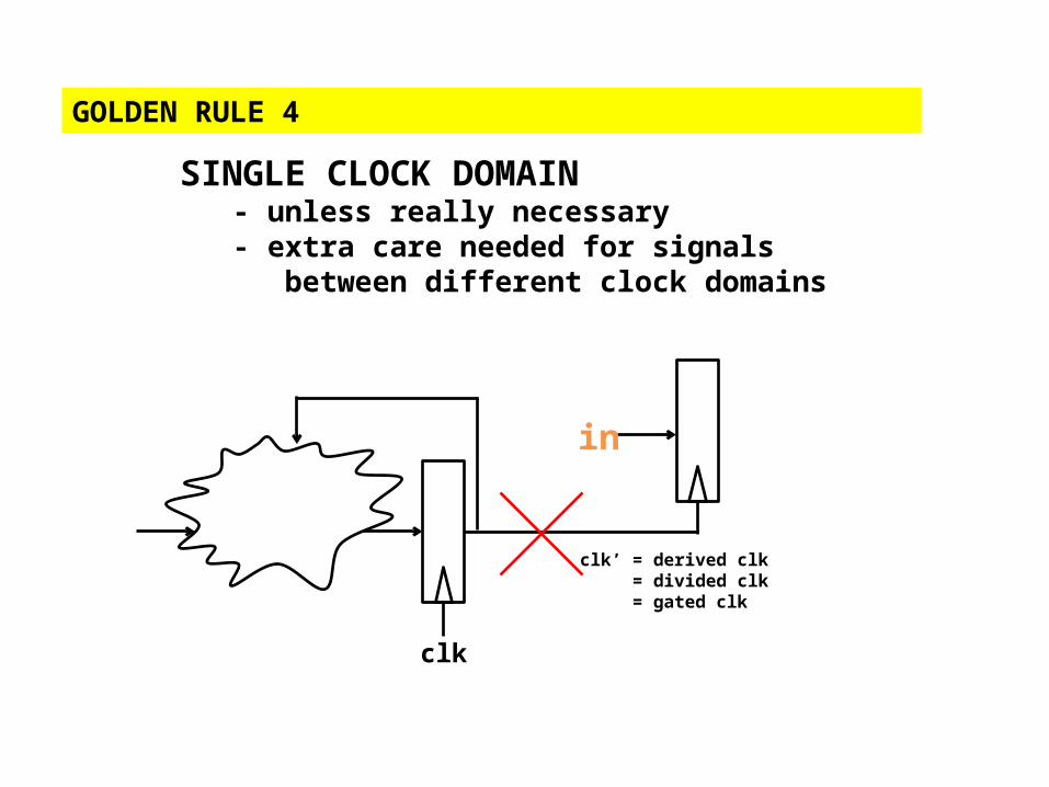
GOLDEN RULE 4
SINGLE CLOCK DOMAIN- unless really necessary- extra care needed for signals
between different clock domains
clk
clk’ = derived clk= divided clk= gated clk
in

GOLDEN RULE 4
Do NOT Write Anything in always @pos blocksother than flop definitionsi.e. Flop <= #1 FlopNxt

GOLDEN RULE 5
SINGLE CLOCK DOMAIN- unless really necessary- extra care needed for signals
between different clock domains
1
0
in
clk
clk

GOLDEN RULE 6
Do NOT Ignore Warning Messagesother then the ones for #1’s.

GOLDEN RULE 7
Write a Testbench and Simulate!It is well worth the time.

HANDLING MULTIPLE CLOCKS
• Clocks with different frequencies• Clocks with same frequency but
different phases between them.

HANDLING MULTIPLE CLOCKS
• Setup Time and Hold Time violations• Metastability
Setup time Hold Time
D
Clock
Stable 0 Stable 1
Metastable state

HANDLING MULTIPLE CLOCKS
• Clock nomenclature• Design partitioning
• One module should work on one clock only• A synchronizer module be made for all
signals that cross from one clock domain to another
Sync 2 to1
Clock1 logic
Sync 1to 2
Clock2 logic
Clock1 domain Clock2 domain
Clk1_SigA
Clk1_SigB
Clk2_SigC
Clk2_SigD

HANDLING MULTIPLE CLOCKS
• Transfer of Control Signals
Src clock domain
Dest clock domain
src_ctrldest_ctrl
dest_clk
Two-stage synchronizer

HANDLING MULTIPLE CLOCKS
• Transfer of DataSignals• Handshake signaling method
X clock domain
Y clock domain
data
xreq
xclk yclk

HANDLING MULTIPLE CLOCKS
• Transfer of DataSignals• Asynchronous FIFO
X clock domain
Y clock domain
Two-stage synchronizerxclk yclk
FIFO
write
fifo_full fifo_empty
read