vlsi presentation final
TRANSCRIPT

Presentation on
DESIGN PROJECTS
EEE 454
VLSI I Laboratory
Prepared By:
Group -1
Naimul Hassan Md. Redwan Islam
Student No – 1006074 Student No - 1006066

DESIGN PROJECT 1:
OPTIMUM DESIGN
OF A 3 INPUT XOR
GATE
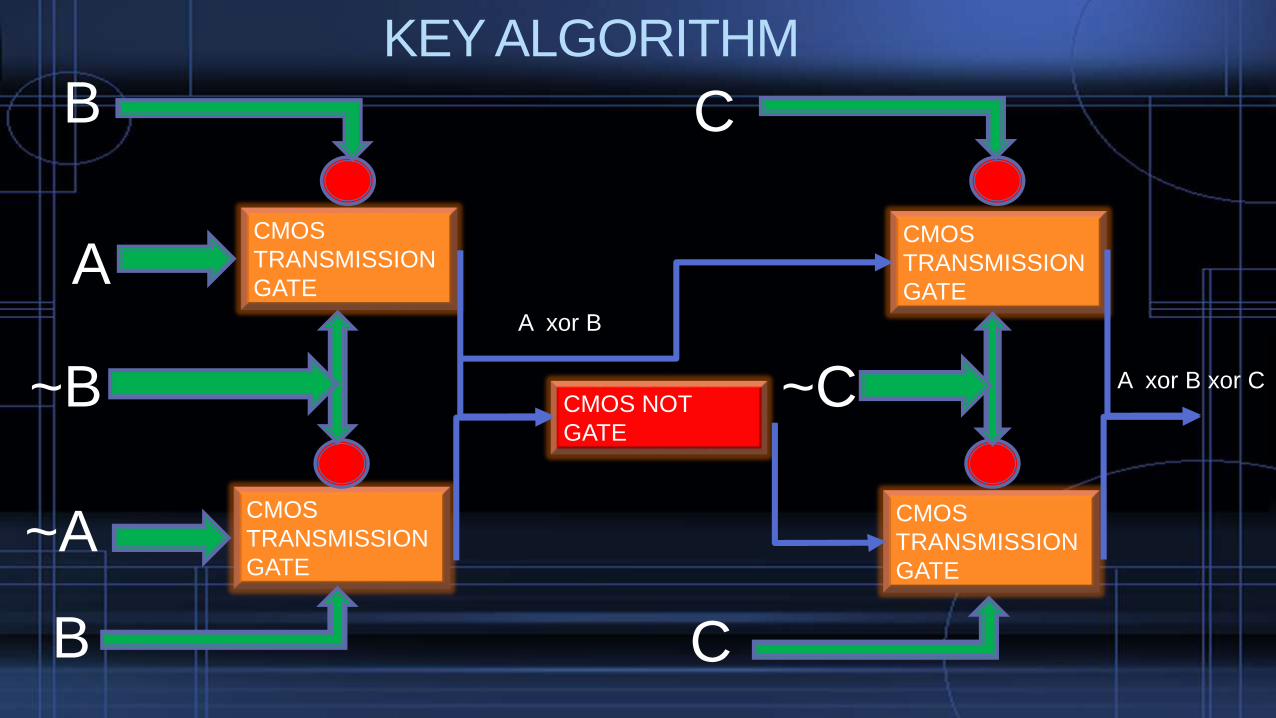
KEY ALGORITHM
CMOS
TRANSMISSION
GATE
CMOS
TRANSMISSION
GATE
CMOS
TRANSMISSION
GATE
CMOS
TRANSMISSION
GATE
CMOS NOT
GATE
B
B
A
~A
~B
C
~C
C
A xor B
A xor B xor C

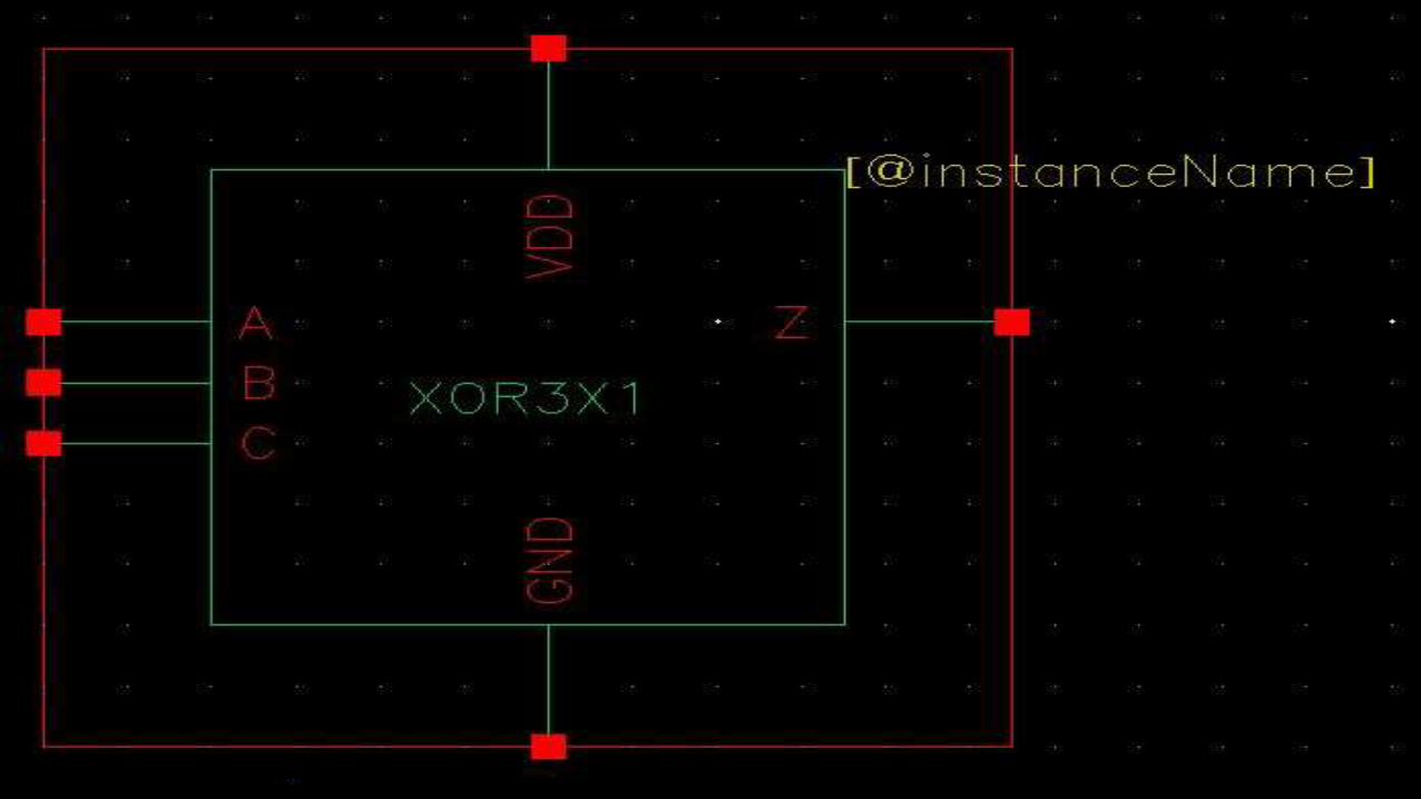
Cadence Schematic of CMOS 3 input XOR gate
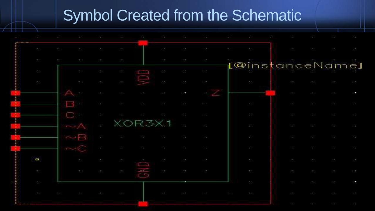
Symbol Created from the Schematic

Simulation Circuit for CMOS 3 input XOR gate
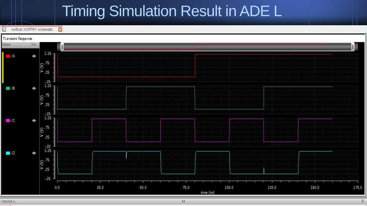
Timing Simulation Result in ADE L
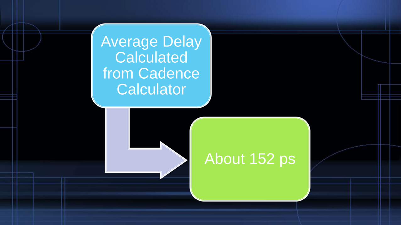
Average Delay Calculated
from Cadence Calculator
About 152 ps

Final Layout Design of CMOS 3 input XOR Gate

Area Calculation of the Layout
Total Length
4.22μm
Total Width
3.27μm
Total Area
13.79μm2

Product of Area and
Propagation delay
318,604.16 μm2 ps2

DESIGN PROJECT 2 :
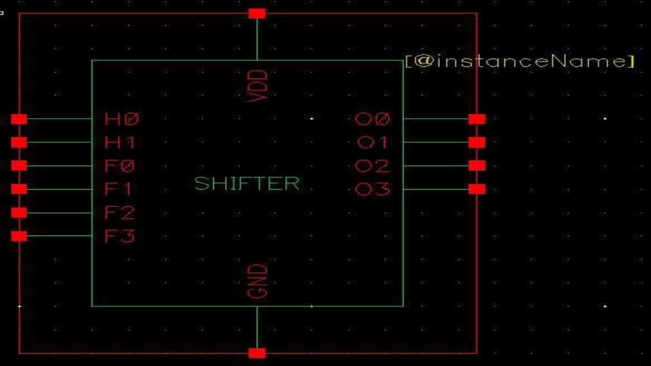
DESIGN OF ALU WITH
SHIFTER
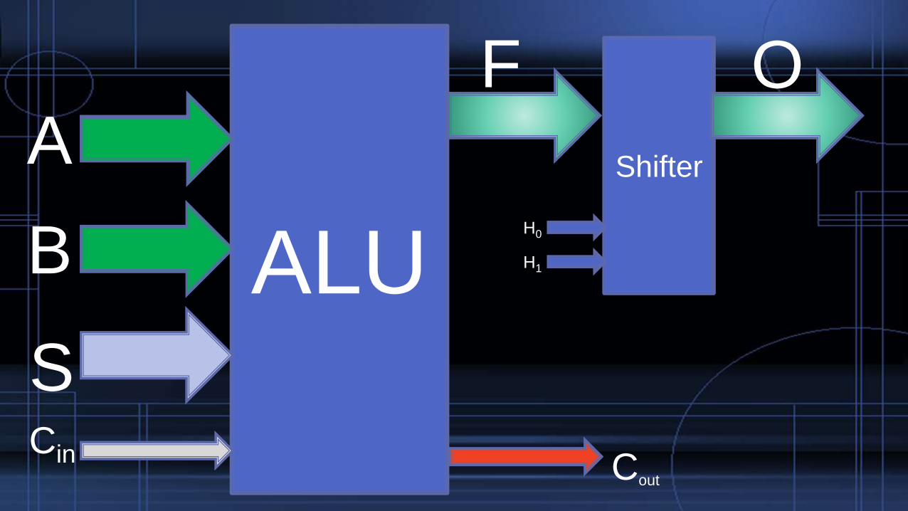
ALU
A
B
SCin
Shifter
H0
H1
F
Cout
O

Operations of the ALUOperation No F Cout
1 A 0
2 A+1 1 if A = 24 -1
3 A+B 1 if (A+B) ≥ 24
4 A+B+1 1 if (A+B) ≥ 24 -1
5 A-B-1 1 if A > B
6 A-B 1 if A ≥ B
7 A-1 1 if A ≠ 0
8 A 1
9 A|B 0
10 A^B 0
11 A&B 0
12 A’ 0
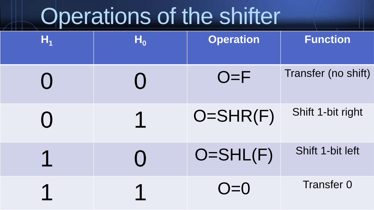
Operations of the shifterH1 H0 Operation Function
0 0 O=F Transfer (no shift)
0 1 O=SHR(F) Shift 1-bit right
1 0 O=SHL(F) Shift 1-bit left
1 1 O=0 Transfer 0
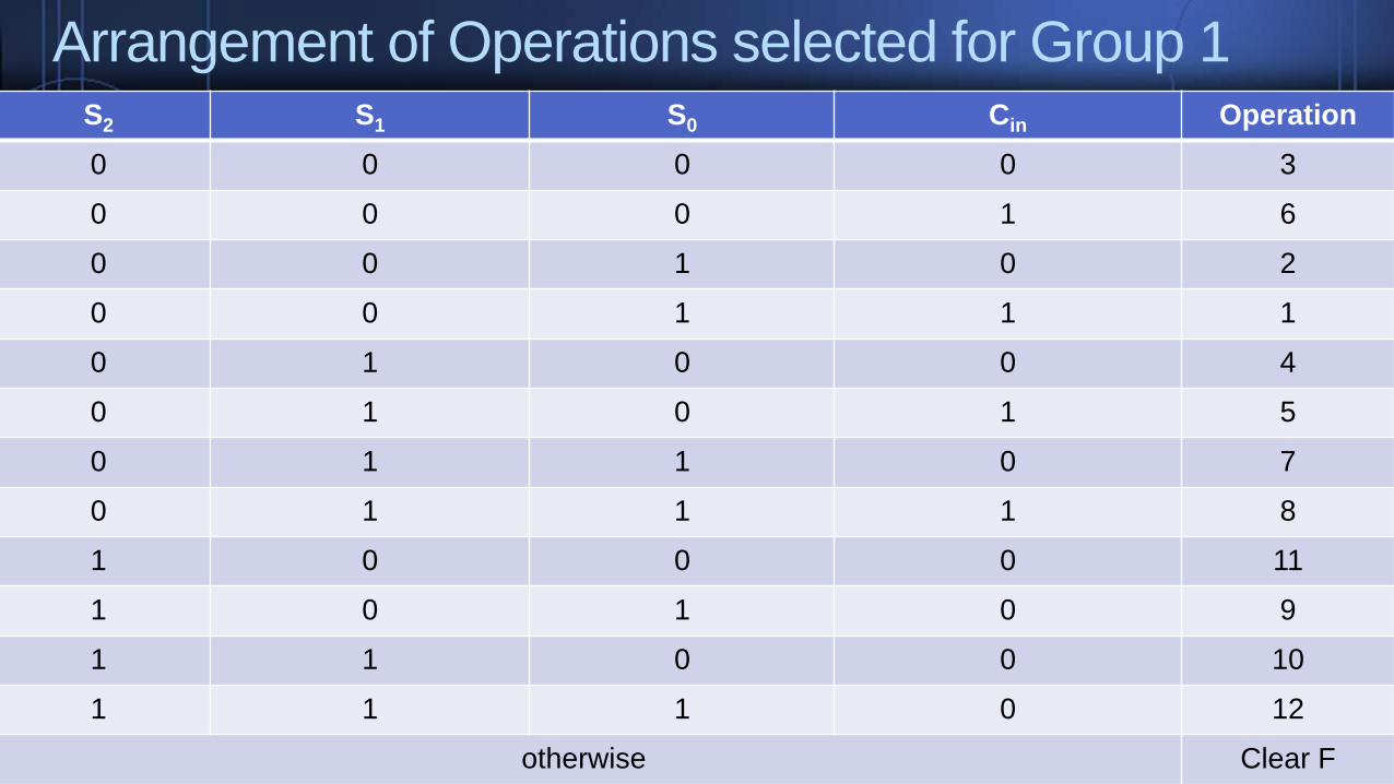
Arrangement of Operations selected for Group 1S2 S1 S0 Cin Operation
0 0 0 0 3
0 0 0 1 6
0 0 1 0 2
0 0 1 1 1
0 1 0 0 4
0 1 0 1 5
0 1 1 0 7
0 1 1 1 8
1 0 0 0 11
1 0 1 0 9
1 1 0 0 10
1 1 1 0 12
otherwise Clear F
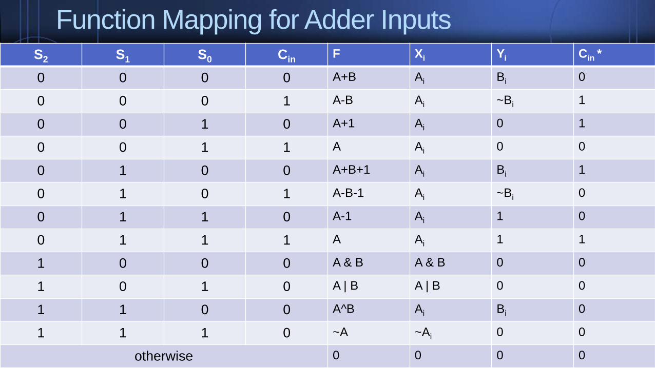
Function Mapping for Adder InputsS2 S1 S0 Cin
F Xi Yi Cin *
0 0 0 0 A+B Ai Bi 0
0 0 0 1 A-B Ai ~Bi 1
0 0 1 0 A+1 Ai 0 1
0 0 1 1 A Ai 0 0
0 1 0 0 A+B+1 Ai Bi 1
0 1 0 1 A-B-1 Ai ~Bi 0
0 1 1 0 A-1 Ai 1 0
0 1 1 1 A Ai 1 1
1 0 0 0 A & B A & B 0 0
1 0 1 0 A | B A | B 0 0
1 1 0 0 A^B Ai Bi 0
1 1 1 0 ~A ~Ai 0 0
otherwise 0 0 0 0
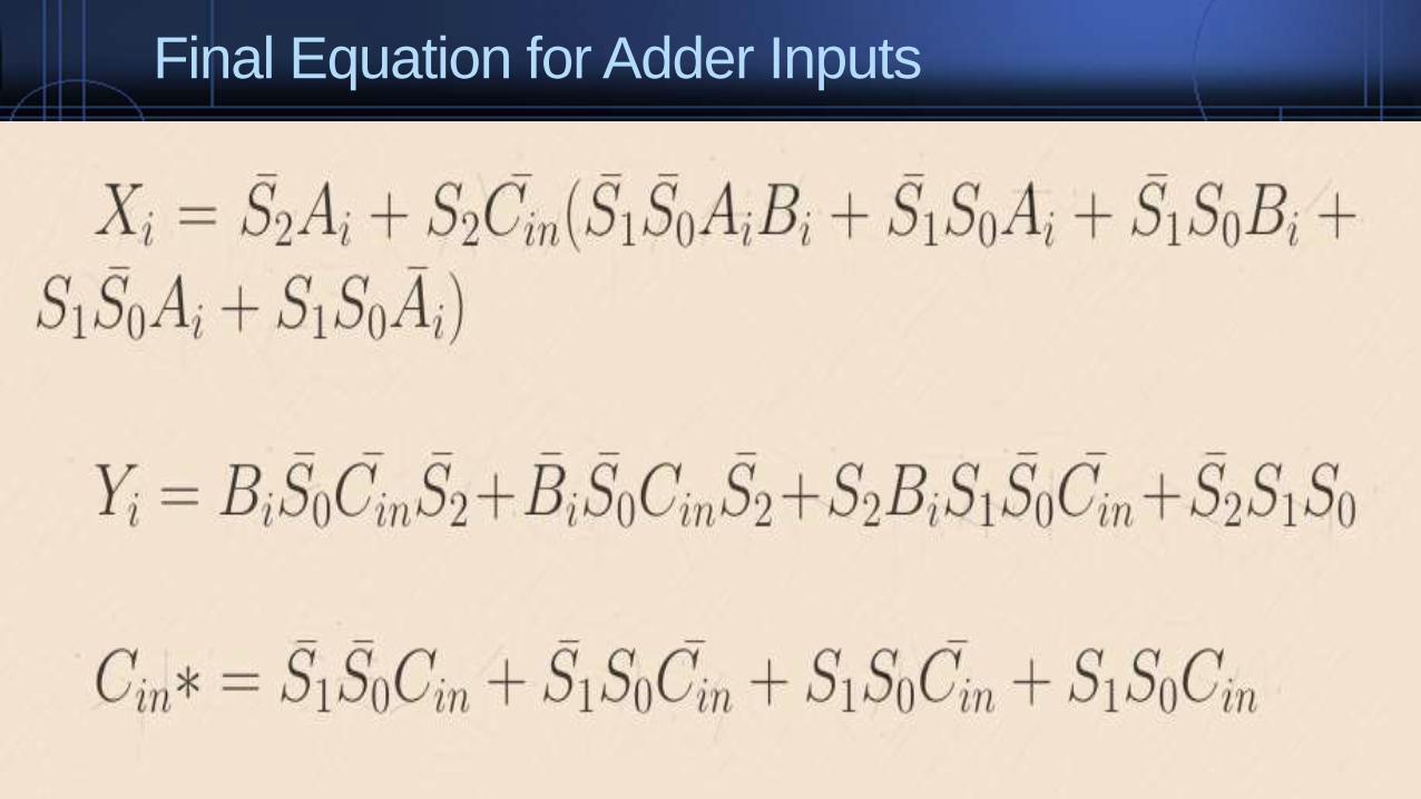
Final Equation for Adder Inputs

SCHEMATICS OF
BASIC GATES

SCHEMATICS OF
LOGIC BLOCKS

Final Schematic for logical simulation

Simulation results

THANKS