via robust self-assembled monolayers high efficiency ... · appear in full in pdf format...
TRANSCRIPT

Subscriber access provided by UNIV TORONTO
Nano Letters is published by the American Chemical Society. 1155 Sixteenth StreetN.W., Washington, DC 20036Published by American Chemical Society. Copyright © American Chemical Society.However, no copyright claim is made to original U.S. Government works, or worksproduced by employees of any Commonwealth realm Crown government in the courseof their duties.
Communication
High Efficiency Colloidal Quantum Dot Photovoltaicsvia Robust Self-Assembled Monolayers
Gi-Hwan Kim, F. Pelayo Garcia de Arquer, Yung jin Yoon, Xinzheng Lan,Mengxia Liu, Oleksandr Voznyy, Zhenyu Yang, Fengjia Fan, Alexander H Ip,
Pongsakorn Kanjanaboos, Sjoerd Hoogland, Jin Young Kim, and Edward H. SargentNano Lett., Just Accepted Manuscript • DOI: 10.1021/acs.nanolett.5b03677 • Publication Date (Web): 28 Oct 2015
Downloaded from http://pubs.acs.org on October 31, 2015
Just Accepted
“Just Accepted” manuscripts have been peer-reviewed and accepted for publication. They are postedonline prior to technical editing, formatting for publication and author proofing. The American ChemicalSociety provides “Just Accepted” as a free service to the research community to expedite thedissemination of scientific material as soon as possible after acceptance. “Just Accepted” manuscriptsappear in full in PDF format accompanied by an HTML abstract. “Just Accepted” manuscripts have beenfully peer reviewed, but should not be considered the official version of record. They are accessible to allreaders and citable by the Digital Object Identifier (DOI®). “Just Accepted” is an optional service offeredto authors. Therefore, the “Just Accepted” Web site may not include all articles that will be publishedin the journal. After a manuscript is technically edited and formatted, it will be removed from the “JustAccepted” Web site and published as an ASAP article. Note that technical editing may introduce minorchanges to the manuscript text and/or graphics which could affect content, and all legal disclaimersand ethical guidelines that apply to the journal pertain. ACS cannot be held responsible for errorsor consequences arising from the use of information contained in these “Just Accepted” manuscripts.

1
High Efficiency Colloidal Quantum Dot Photovoltaics via Robust Self-
Assembled Monolayers
Gi-Hwan Kim†,‡,§, F. Pelayo García de Arquer
†,§, Yung Jin Yoon‡, Xinzheng Lan
†, Mengxia Liu
†,
Oleksandr Voznyy†, Zhenyu Yang
†, Fengjia Fan
†, Alexander H. Ip
†, Pongsakorn Kanjanaboos
†,
Sjoerd Hoogland†, Jin Young Kim
*,‡, Edward H. Sargent
*,†
†Department of Electrical and Computer Engineering, University of Toronto, 10 King’s
College Road, Toronto, Ontario, M5S 3G4, Canada
‡School of Energy and Chemical Engineering, Ulsan National Institute of Science and
Technology (UNIST) Ulsan 689-798, South Korea
§ Indicates equal contribution
E-mail: [email protected], [email protected]
Page 1 of 29
ACS Paragon Plus Environment
Nano Letters
123456789101112131415161718192021222324252627282930313233343536373839404142434445464748495051525354555657585960

2
Table of Contents
High Efficiency Colloidal Quantum Dot Photovoltaics via Robust Self-Assembled Monolayers
Page 2 of 29
ACS Paragon Plus Environment
Nano Letters
123456789101112131415161718192021222324252627282930313233343536373839404142434445464748495051525354555657585960
3
Abstract
The optoelectronic tunability offered by colloidal quantum dots (CQDs) is attractive for
photovoltaic applications, but demands proper band alignment at electrodes for efficient
charge extraction at minimal cost to voltage. With this goal in mind, self-assembled
monolayers (SAMs) can be used to modify interface energy levels locally. However, to be
effective, SAMs must be made robust to treatment using the various solvents and ligands
required for to fabricate high quality CQD solids. We report robust self-assembled
monolayers (R-SAMs) that enable us to increase the efficiency of CQD photovoltaics. Only
by developing a process for secure anchoring of aromatic SAMs, aided by deposition of the
SAMs in a water-free deposition environment, were we able to provide an interface
modification that was robust against the ensuing chemical treatments needed in the
fabrication of CQD solids. The energy alignment at the rectifying interface was tailored by
tuning the R-SAM for optimal alignment relative to the CQD quantum-confined electron
energy levels. This resulted in a CQD PV record power conversion efficiency (PCE) of
10.7% with enhanced reproducibility relative to controls.
Keywords: Quantum Dot Solar Cells, high performance, R-SAM, robust, interface, dipole
moment.
Page 3 of 29
ACS Paragon Plus Environment
Nano Letters
123456789101112131415161718192021222324252627282930313233343536373839404142434445464748495051525354555657585960

4
Colloidal quantum dot (CQD) materials are prominent candidates for optoelectronic and
photovoltaic applications in view of their tunable bandgap, ease of processing, low cost, stability
and large-area deployability.1-6
Of particular interest are lead chalcogenide nanocrystals (e.g. PbS
and PbSe) whose bandgap can be tailored across the wide solar spectrum.7, 8
The performance of
CQD photovoltaic devices has seen progress since their advent and, driven by the advances in the
materials science of the CQD solid9 and the engineering of improved devices,
10, 11 certified power
conversion efficiencies (PCE) approaching 10% have recently been reported.12, 13
Now that short-circuit current densities as high as 30 mA/cm2 have been recently demonstrated,
14
a leading opportunity for further progress lies in improving the open circuit voltage (VOC), which
today shows a considerable deficit compared, for example, to the impressively low (Eg-qVoc) of
perovskites solar cells.15
To exploit the bandgap tunability endowed by quantum confinement, it
is important to achieve proper band alignment at the interface with the different electron/hole
blocking layers– a challenging requirement given the finite choice of high-performance metal-
oxide electrodes.
Self-assembled monolayers (SAMs) have been extensively used in dye-sensitized and
organic solar cells to tailor the energy levels at different material interfaces.16, 17
This is enabled
by the electrostatic potential established by the molecule’s dipole that results in an effective shift
of the local vacuum level. If properly engineered, this can be used to tailor the photovoltaic
figures of merit in devices.
To introduce SAMs to produce highly efficient CQD solar cells represents a significant
challenge, since the sequential use of different solvents and chemically active ligands such as
thiols and halides is required for CQD film processing subsequent to SAM application,12
and this
is prone to result in SAM damage.18, 19
Successful interface engineering thus requires the SAM be
Page 4 of 29
ACS Paragon Plus Environment
Nano Letters
123456789101112131415161718192021222324252627282930313233343536373839404142434445464748495051525354555657585960

5
resistant to the chemical reagents used during film formation, be homogeneous, and be highly
reproducible.
In this work we explore, for the first time, the joint engineering of SAM-tailored interfaces
and CQD bandgap, ultimately producing photovoltaic devices with a new record PCE of 10.7%.
This is achieved by the manipulation of the interface between CQD active layer and the electron
transport layer using a suite of benzoic-acid-functionalized SAMs that we have developed with
the goal of uncompromised quality during ensuing device fabrication. Only by developing a
process for secure anchoring of aromatic SAMs, aided by the use of a water-free deposition
environment, we were able to provide an interface modification that was robust against ensuing
chemical treatments needed in the fabrication of CQD solids. The increased PCE is a result of the
improved VOC, a record for a high-performing CQD PV cell at 0.66 V, due to the dipole moment
imparted by the monolayer.17
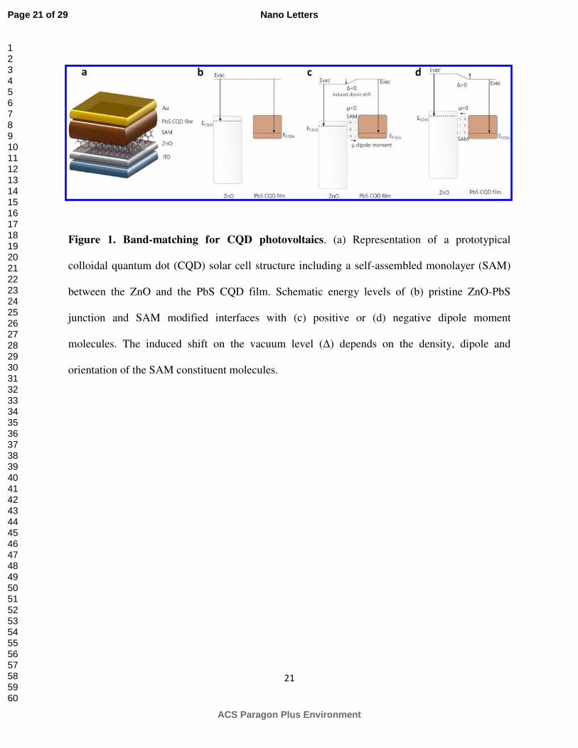
The structure of the CQD photovoltaic devices is shown in Figure 1a. Briefly (for detailed
fabrication see Experimental section), a ZnO layer is deposited by spin-casting on top of an
indium tin oxide (ITO) electrode. These electrodes are then functionalized using various SAMs,
each of which employs a carboxylic acid binding group known to attach to metal oxide
semiconductors such as ZnO.20, 21
The photoactive CQD film is subsequently deposited in layer-
by-layer fashion. The originally oleic-acid capped CQDs are subject to a solution-phase iodine
treatment and then fully exchanged during film formation using tetrabutylammoniun iodide
(TBAI) as previously reported.10-12
An electron blocking layer consisting of 2 layers of 1,2-
ethanedithiol (EDT) exchanged CQDs is spin-cast prior to application of a gold electrode
contact.11
Page 5 of 29
ACS Paragon Plus Environment
Nano Letters
123456789101112131415161718192021222324252627282930313233343536373839404142434445464748495051525354555657585960

6
It is known that the molecular dipole (µmol) can be adjusted in magnitude and direction by
judiciously varying the functionality at the opposite site of the carboxylic group.17
In this a way,
the energy levels of the ZnO substrate can be tailored (Figure 1b). For example, molecules
exhibiting a positive dipole moment are expected to produce a downward shift of the vacuum
level at the interface (Figure 1c). In contrast, negative dipole moment molecules will push the
ZnO energy levels upward (Figure 1d). The effective net energy shift (∆) is a function of the
SAM density (N) and orientation (θ), in such a way interfacial energy levels can be finely
controlled:17, 18
∆=�������(�)
���� (eq. 1)
Here q, ε0 and εr are respectively the elementary charge, vacuum and relative permittivity of the
molecules. If properly mastered, SAMs can be used to match the optimum energy levels at the
ZnO interface, leading to maximized open-circuit voltage.
To evaluate the conditions for chemically-stable SAMs during CQD device fabrication, we
functionalized ZnO substrates using a suite of different SAMs, and subjected them to the
relevant ensuing CQD-processing chemical steps. SAMs were built by immersing the as-
deposited ZnO substrates into solutions of the different molecules (see experimental section for
details on SAM fabrication). 3-Nitropropionic acid (NPA) and 4-Nitrobenzoic acid (NBA) were
chosen in view of their similar functional characteristics (carboxylic and nitro groups) and dipole
moments, but different morphologies (aliphatic versus aromatic character). The presence of the
SAMs after incubation was first assessed using XPS measurements (Figure S1 and S2). We then
subjected the functionalized ZnO substrates to CQD solid film fabrication conditions: a
Page 6 of 29
ACS Paragon Plus Environment
Nano Letters
123456789101112131415161718192021222324252627282930313233343536373839404142434445464748495051525354555657585960
7
sequential combination of ligands (tetrabutylammonium iodide, TBAI) and orthogonal solvents
(methanol and octane).11, 12
We were concerned that these treatments could potentially lead to
SAM degradation by the halogenation of its constituent molecules, the modification of their
anchoring mode, or the substitution of coordinated ZnO-COOH bonds.22, 23
We found that, after we exposed the SAMs to TBAI and methanol, NPA SAMs were
indeed damaged, as revealed by XPS measurements (Figure 2a). In contrast, NBA SAMs remain
present following the same fabrication conditions, as no modification in either XPS peak position
or intensity was evident. This suggests that the structure of the SAM molecules plays a
significant role in determining the robustness of SAMs during ensuing CQD film processing. We
propose that this may arise from the strong π-π interaction taking place between the conjugated
benzene rings that ultimately leads to a more ordered and uniformly oriented SAM sterically
protected against attacking reagents (Figure 2b). In contrast, aliphatic SAMs exhibit more
degrees of freedom resulting in less ordered SAMs and the exposure of a higher number of
reactive sites. This could result in damage to the SAM, since aliphatic molecules are more prone
to iodide halogenation compared to the aromatic molecules.24, 25
These studies led us to select aromatic molecules as the candidate family for robust SAMs
compatible with high-efficiency CQD photovoltaics.
In order to ensure the compactness and reproducibility of the SAM substrate modification
— a crucial aspect that needs to be assessed for photovoltaic applications — we then
investigated different assembly conditions. During the formation of the SAM, several competing
processes, such as the adsorption of water or oxygen species, can undermine self-assembly,
resulting in molecule clustering and incomplete SAM morphologies.26
These would fail to
provide the spatially uniform and reliable increase desired in solar cell performance. The
Page 7 of 29
ACS Paragon Plus Environment
Nano Letters
123456789101112131415161718192021222324252627282930313233343536373839404142434445464748495051525354555657585960

8
problem is evidenced in Figure 2c, in which atomic force microscopy (AFM) reveals the
presence of molecule aggregates in the case of substrates incubated under ambient environmental
conditions.
In striking contrast, inert incubation leads to uniform, pinhole-free, SAMs. Kelvin probe
microscopy reveals that the air-processed SAMs showed uncontrolled work functions, while
SAMs applied in an inert environment showed a much narrower distribution of electronic
properties (Figure 2d).
In sum, only by combining aromatic SAMs and inert processing conditions (R-SAM) were
we able to obtain reproducible SAMs that were robust against CQD film processing.
In order to modify the energy level of the ZnO in a controlled way, different moieties were
incorporated to the benzene ring to modify its associated dipole moment (-NO2, 4-nitro benzoic
acid (NBA), +3.8D and –NH2, 4-aminobenzoic acid (ABA) , -4.5D). The different vacuum level
shift at the ZnO surface after R-SAM treatment was assessed using ultraviolet photoelectron
spectroscopy (UPS). Figure 2e reveals the modification in the vacuum level following R-SAM
formation. A consistent trend is observed correlating with the opposite sign of NBA and ABA
molecule dipoles (see inset).
The concentration of the R-SAM and the associated energy shift was controlled using
different concentrations during the incubation procedure (see Experimental section). Contact
angle measurements were carried out to corroborate the different monolayer coverage at various
ABA or NBA concentrations (Figure S3). The increase in the contact angle observed under
heavier treatments indicates a greater hydrophobicity of the ZnO substrates, consistent with
increased R-SAM coverage.17, 27
Page 8 of 29
ACS Paragon Plus Environment
Nano Letters
123456789101112131415161718192021222324252627282930313233343536373839404142434445464748495051525354555657585960

9
Figure 2f shows the work function of the functionalized substrates for various NBA/ABA
concentrations compared to that of the bare ZnO substrate as measured by Kelvin-probe force
microscopy. Following ABA treatment, the work function decreases by up to 0.2 eV. In contrast,
the work function of NBA functionalized substrates is pushed down by 0.4 eV for the highest of
the NBA concentrations. This trend is in good agreement with the expected behavior revealed by
UPS (see Figure S4).
To evaluate the impact that the R-SAM dipole could have on solar cell performance, we
built an optoelectronic model that takes into account relevant material parameters such as solar
light absorption, energy levels, transport and density of states (see Table S1 for modelling
details). By doing so, we could determine the relation between CQD exciton energy and ZnO
electron affinity in the overall optimization of PCE. In Figure 3a, we plot the calculated PCE as
a function of CQD exciton energy and induced dipole shift. In the absence of a dipole layer, the
simulated PCE peaks for a CQD exciton peak at 1.3-1.5 eV. Encouragingly, under these
conditions, electrostatic modification of the ZnO/CQD PbS interface could result in a further
improvement of 1 PCE point, if molecules with a positive dipole are used. This comes as a
consequence of the associated improvement in the open-circuit voltage (Figure 3b), which
increases from a baseline value of 0.66 V under the presence of a positive dipole shift (increasing
the local vacuum energy; e.g. using ABA R-SAMs). A maximum VOC increase of 90 mV is
feasible, beyond which further increasing the dipole shift results in a significant reduction of
electron injection and short-circuit current, and this pins the attainable open-circuit voltage and
leads to a decrease in the net PCE (the complete set of photovoltaic figures of merit is shown in
Figure S5). Both control and R-SAM modified devices retain their stability and show hysteresis-
free behavior when stored in ambient conditions over the course of an initial 30 day study
Page 9 of 29
ACS Paragon Plus Environment
Nano Letters
123456789101112131415161718192021222324252627282930313233343536373839404142434445464748495051525354555657585960
10
(Figure S6-S7). The use of molecules with a negative dipole (e.g. NBA) is expected to result
into a rapid reduction in the open-circuit voltage. The aforementioned scenario is illustrated in
Figure 3c, where the VOC variation under the presence of different induced dipole shifts is
depicted.
We then sought to take advantage of vacuum level modulation offered by the R-SAM: we
fabricated photovoltaic devices based on ZnO dipole-engineered substrates and CQDs exhibiting
an excitonic peak at 1.41 eV. Current density vs. voltage characteristics under 100 mW/cm2
AM1.5G irradiation of devices prepared on ABA (negative dipole moment), NBA (positive
dipole moment) and pristine ZnO substrates are shown in Figure 4a (device performance
summarized in Table 1). As hypothesized, the modification of the energy level after ABA
treatment (0.01%) gives rise to a notable increase in VOC, and this reaches a new record value of
0.66 V. An improvement in FF is also observed due to reduced back-recombination. As a
consequence, the solar PCE is enhanced from 10.2% to 10.7%. This is the highest PCE reported
to date for a CQD photovoltaic device. In contrast, when NBA R-SAMs are used, both VOC and
PCE decrease, a fact attributed to the opposite orientation of their dipole moments. The
performance of cells for various concentrations of ABA and NBA is shown in Figure S8 and
their figures of merit listed in Table S2 and S3.
To further investigate the effects of ABA interface modification, as well their
reproducibility, we characterized the performance of over 50 cells subjected to ABA R-SAM
modification. A box-plot of the open-circuit voltage as a function of ABA concentration is
shown in Figure 4b. This diagram reveals a consistent improvement over the control case once
R-SAMs are used. A histogram of the PCE for both optimized and reference samples is shown in
Figure 4c. We report an average PCE of 9.8% (± 0.4%) for standard devices, and a PCE of
Page 10 of 29
ACS Paragon Plus Environment
Nano Letters
123456789101112131415161718192021222324252627282930313233343536373839404142434445464748495051525354555657585960

11
10.2% (± 0.4%) for optimized ABA R-SAMs. The external quantum efficiency (EQE) of a
representative ABA 0.01% device is shown in Figure 4d, illustrating the high EQE at the
exciton peak (up to 60%) and the good agreement between predicted and measured JSC.
Based on our predictions (Figure 3a), we then sought to verify that the interface
modification using R-SAMs could be exploited for other CQD sizes. We built devices based on
smaller-bandgap CQDs (1.3 eV exciton energy, Figure S9). An additional 0.75 power point was
obtained due to the increase in VOC (plus 20 mV, raising VOC up to 0.6 V) and FF (+0.02). This
showcases the opportunity for R-SAMs to extend further PV response into the infrared region via
band alignment tailoring.28
Page 11 of 29
ACS Paragon Plus Environment
Nano Letters
123456789101112131415161718192021222324252627282930313233343536373839404142434445464748495051525354555657585960

12
Conclusion
This work constitutes the first report in which interface-modifying SAMs led to enhanced
CQD PV performance. R-SAMs take advantage of the strong π-π interaction of benzene rings,
enabling them to withstand the otherwise damaging effects of CQD film ligand exchange
processing. The secure anchoring of aromatic R-SAMs, aided by the use of assembly in an inert
environment, resulted in reproducible interface modification that was robust against ensuing
chemical treatments needed in the fabrication of CQD solids. By incorporating R-SAMs
consisting of amine or nitro functional groups, we tailored band alignment advantageously at the
PbS-CQD/ZnO interface. This led to a record PCE of 10.7%, primarily due to improvements in
VOC (up to 0.66 V) and FF. We jointly explored R-SAM interface modification and quantum dot
tunability, demonstrating that the aforementioned benefits also hold for different CQD bandgaps.
This suggests avenues for further improvements such as the incorporation of R-SAMs in tandem
CQD architectures that maximize solar energy harvesting.7, 8
Page 12 of 29
ACS Paragon Plus Environment
Nano Letters
123456789101112131415161718192021222324252627282930313233343536373839404142434445464748495051525354555657585960

13
Experimental
CQD synthesis:
PbS QDs were prepared following previous reports.5 The nanoparticles were separated
from the growth solution by using acetone and then dried in vacuum and redispersed in toluene
(150 mg/mL) and transferred to a nitrogen glovebox. Methanol was used to precipitate the
nanocrystals then centrifuged to isolate the PbS nanoparticles. This washing step was repeated
several times. Following ful drying, the nanocrystals were finally dispersed in octane (50
mg/mL). Iodine molecular passivation was following the previous reported.12
ZnO film deposition:
The synthesis of ZnO nanoparticles is similar to previously reported method.21
After the
synthesis of ZnO. ZnO solution is kept at room temperature for 24 hr with vigorous stirring. For
the ZnO film, the ZnO solution was spin-cast on ITO glass at 3,000 rpm for 30 s then annealing
the substrate at 200℃ for 10 min.
R-SAM fabrication:
Robust self-assembled monolayers were fabricated by soaking ZnO substrates into SAM
molecules solutions (ABA and NBA were dissolved in anhydrous methanol under a N2
atmosphere) for 1 min and then rinsed in pure methanol after incubation. Substrates were then
annealed at 100℃ for 10 min. The fabrication method was optimized to ensure compatibility
Page 13 of 29
ACS Paragon Plus Environment
Nano Letters
123456789101112131415161718192021222324252627282930313233343536373839404142434445464748495051525354555657585960

14
with subsequent CQD processing steps, as well as to provide with a good reproducibility (see
Figure S10).
Device fabrication:
PbS CQD films were fabricated by a layer-by-layer spin-casting process. PbS CQDs in
octane (50 mg/mL) were deposited onto the ZnO substrates and spin-casted at 2500 rpm for 10 s.
TBAI (10 mg/mL) in methanol solution was deposited on the PbS CQD film and spun after 30 s
at the same speed for 10 s then followed by two rinsing steps with methanol. The process was
repeated 8 times. After completion of the PbS-TBAI layer, two layers of ethane dithiol (EDT)
exchanged CQDs (0.01 vol% in acetonitrile solution) were deposited. For the top electrode, 120
nm Au was deposited on the PbS CQD film for making complete the device.
Device characterization:
J-V characterization: The current–voltage characteristics were measured using a Keithley 2400
source-meter in N2 atmosphere. The solar spectrum at AM1.5 was simulated to within class A
specifications (less than 25 % spectral mismatch) with a Xe lamp and filters (Solar Light
Company Inc.) with measured intensity at 100 mW/cm2. The source intensity was measured
using a Melles–Griot broadband power meter and a Thorlabs broadband power meter through a
circular 0.049 cm2 aperture at the position of the device and confirmed with a calibrated
reference solar cell (Newport, Inc.). The accuracy of the power measurement was estimated to be
±5%.
Page 14 of 29
ACS Paragon Plus Environment
Nano Letters
123456789101112131415161718192021222324252627282930313233343536373839404142434445464748495051525354555657585960
15
EQE measurement: External-quantum-efficiency spectra were taken by subjecting the cells to
monochromatic illumination (400 W Xe lamp passing through a monochromator and appropriate
cut-off filters). The output power was calibrated with Newport 818-UV and Newport 838-IR
photodetectors. The beam was chopped at 220 Hz and focused in the pixel together with a solar-
simulator at 1 sun intensity to provide for light bias. The response of the cell was acquired with a
Lakeshore pre-amplifier connected to Stanford Research 830 lock-in amplifier at short-circuit
conditions.
XPS and UPS measurement: XPS and UPS measurements were carried out using a ESCALAB
250XI from Thermo Fisher Scientific. He I hv = 21.22 eV was used as a light source and
thermally evaporated Au substrates were used as a reference for UPS. Workfunctions (Φ) were
calculated from the onset of the secondary edge (ESE) using the equation Φ = 21.22 - ESE.
Valence band edges were taken relative to an Au reference with known Fermi energy.29
Electrical Modeling: CQD photovoltaic devices were modelled with SCAPS30, 31
simulation
software. Parameter space and simulation details are available in Table S1.
Page 15 of 29
ACS Paragon Plus Environment
Nano Letters
123456789101112131415161718192021222324252627282930313233343536373839404142434445464748495051525354555657585960

16
ASSOCIATED CONTENT
Supporting Information. A detailed description of XPS, UPS contact angle, J-V characteristics,
with various concentrations of ABA and NBA on ZnO substrate, as well as additional electrical
modelling and histogram of performance with different fabrications can be found in the
Supporting Information. This material is available free of charge via the Internet at
http://pubs.acs.org.
AUTHOR INFORMATION
Corresponding Author
* E-mail: [email protected] (E. H. Sargent), [email protected] (J. Y. Kim)
Author Contributions
Dr. Gi-Hwan Kim and Dr. F. Pelayo García de Arquer equally contributed to this work. All
authors discussed the results and assisted during manuscript preparation.
Notes
The authors declare no competing financial interest.
Acknowledgement
This publication is based in part on work supported by Award KUS-11-009-21, made by King
Abdullah University of Science and Technology (KAUST), by the Ontario Research Fund -
Research Excellence Program, and by the Natural Sciences and Engineering Research Council
(NSERC) of Canada, by the International Cooperation of the Korea Institute of Energy
Technology Evaluation and Planning (KETEP) grant funded by the Korea government Ministry
of Knowledge Economy (2012T100100740). We thank Emre Yassitepe, Cao-Thang Dinh for
Page 16 of 29
ACS Paragon Plus Environment
Nano Letters
123456789101112131415161718192021222324252627282930313233343536373839404142434445464748495051525354555657585960

17
helpful discussions. We also thank E. Palmiano, L. Levina, A. Labelle, R. Wolowiec and D.
Kopilovic for their help over the course of this study.
Page 17 of 29
ACS Paragon Plus Environment
Nano Letters
123456789101112131415161718192021222324252627282930313233343536373839404142434445464748495051525354555657585960
18
References
1. Hines, M. A.; Scholes, G. D. Adv. Mater. 2003, 15, 1844-1849.
2. Gur, I.; Fromer, N. A.; Geier, M. L.; Alivisatos, A. P. Science 2005, 310, 462-465.
3. Mcdonald, S. A.; Konstantatos, G.; Zhang, S.; Cyr, P. W.; Klem, E. J.; Levina, L.;
Sargent, E. H. Nat. Mater. 2005, 4, 138-142.
4. Kamat, P. V. J. Phy. Chem. C 2008, 112, 18737-18753.
5. Pattantyus-Abraham, A. G.; Kramer, I. J.; Barkhouse, A. R.; Wang, X.; Konstantatos, G.;
Debnath, R.; Levina, L.; Raabe, I.; Nazeeruddin, M. K.; Grätzel, M. ACS nano 2010, 4,
3374-3380.
6. Kim, G. H.; Walker, B.; Kim, H. B.; Kim, J. Y.; Sargent, E. H.; Park, J.; Kim, J. Y. Adv.
Mater. 2014, 26, 3321-3327.
7. Sargent, E. H. Nat. Photon. 2012, 6, 133-135.
8. Graetzel, M.; Janssen, R. A.; Mitzi, D. B.; Sargent, E. H. Nature 2012, 488, 304-312.
9. Ip, A. H.; Thon, S. M.; Hoogland, S.; Voznyy, O.; Zhitomirsky, D.; Debnath, R.; Levina,
L.; Rollny, L. R.; Carey, G. H.; Fischer, A. Nat. Nanotech. 2012, 7, 577-582.
10. Ning, Z.; Voznyy, O.; Pan, J.; Hoogland, S.; Adinolfi, V.; Xu, J.; Li, M.; Kirmani, A. R.;
Sun, J.-P.; Minor, J.; Kemp, K. W.; Dong, H.; Rollny, L.; Labelle, A.; Carey, G.;
Sutherland, B.; Hill, I.; Amassian, A.; Liu, H.; Tang, J.; Bakr, O. M.; Sargent, E. H. Nat.
Mater. 2014, 13, 822-828.
11. Chuang, C.-H. M.; Brown, P. R.; Bulović, V.; Bawendi, M. G. Nat. Mater. 2014, 13, 796-
801.
12. Lan, X, Voznyy, O., Kiani, A., F. Pelayo García de Arquer, Abdullah, S. A., Kim, G. H.,
Liu, M., Yang, Z., Walters, G., Jixian X., Yuan, M., Ning, Z., Fan, F., Kanjanaboos, P.,
Page 18 of 29
ACS Paragon Plus Environment
Nano Letters
123456789101112131415161718192021222324252627282930313233343536373839404142434445464748495051525354555657585960

19
Kramer, i., Zhitomirsky, D., Lee, P., Perelgut, A., Hoogland, S., Sargent, E. H. Adv. Mater.
2015, DOI: 10.1002/adma.201503657
13. http://www.nrel.gov/ncpv/. (access date) 2015, October, 16.
14. Carey, G. H.; Levina, L.; Comin, R.; Voznyy, O.; Sargent, E. H. Adv. Mater. 2015, 27,
3325-3330.
15. Yang, W. S.; Noh, J. H.; Jeon, N. J.; Kim, Y. C.; Ryu, S.; Seo, J.; Seok, S. I. Science 2015,
348, 1234-1237.
16. Krüger, J.; Bach, U.; Grätzel, M. Adv. Mater. 2000, 12, 447-451.
17. Goh, C.; Scully, S. R.; McGehee, M. D. J. Appl. Phy. 2007, 101, 114503-114503.
18. Love, J. C.; Estroff, L. A.; Kriebel, J. K.; Nuzzo, R. G.; Whitesides, G. M. Chem. Rev.
2005, 105, 1103-1170.
19. Tekin, N.; Cebe, M.; Tarımcı, Ç. Chem. Phy. 2004, 300, 239-246.
20. Moreira, N.; Garcia, A.; Rosa, A.; Frauenheim, T. In Functionalization of ZnO surfaces
with organic molecules, SPIE OPTO, 2012; International Society for Optics and
Photonics: pp 826312-826314.
21. Jagadamma, L. K.; Abdelsamie, M.; El Labban, A.; Aresu, E.; Ndjawa, G. O. N.; Anjum,
D. H.; Cha, D.; Beaujuge, P. M.; Amassian, A. J. Mater. Chem. A 2014, 2, 13321-13331.
22. Anderson, N. C.; Hendricks, M. P.; Choi, J. J.; Owen, J. S. J. Am. Chem. Soc. 2013, 135,
18536-18548.
23. Anderson, N. C.; Owen, J. S. Chem. Mater. 2012, 25, 69-76.
24. Lange, I.; Reiter, S.; Pätzel, M.; Zykov, A.; Nefedov, A.; Hildebrandt, J.; Hecht, S.;
Kowarik, S.; Wöll, C.; Heimel, G. Adv. Func. Mater. 2014, 24, 7014-7024.
Page 19 of 29
ACS Paragon Plus Environment
Nano Letters
123456789101112131415161718192021222324252627282930313233343536373839404142434445464748495051525354555657585960
20
25. Gliboff, M.; Li, H.; Knesting, K. M.; Giordano, A. J.; Nordlund, D.; Seidler, G. T.;
Brédas, J.-L.; Marder, S. R.; Ginger, D. S. J. Phy. Chem. C 2013, 117, 15139-15147.
26. Moreira, N. H.; Domıinguez, A.; Frauenheim, T.; da Rosa, A. L. Phy. Chem. Chem. Phy.
2012, 14, 15445-15451.
27. Choi, H.; Kim, H. B.; Ko, S. J.; Kim, J. Y.; Heeger, A. J. Adv. Mater. 2015, 27, 892-896.
28. Ip, A. H.; Kiani. K.; Kramer. I. J; Voznyy, O.; Movahed. H. F.; Levina. L.; Adachi. M.
M.; Hoogland, S.; Sargent, E. H. ACS nano 2015, 9, 8833-8842.
29. Braun, S.; Salaneck, W. R.; Fahlman, M. Adv. Mater 2009, 21, 1450-1472.
30. Burgelman, M.; Nollet, P.; Degrave, S. Thin Solid Films 2000, 361, 527-532.
31. Burgelman, M.; Decock, K.; Khelifi, S.; Abass, A. Thin Solid Films 2013, 535, 296-301.
Page 20 of 29
ACS Paragon Plus Environment
Nano Letters
123456789101112131415161718192021222324252627282930313233343536373839404142434445464748495051525354555657585960
21
Figure 1. Band-matching for CQD photovoltaics. (a) Representation of a prototypical
colloidal quantum dot (CQD) solar cell structure including a self-assembled monolayer (SAM)
between the ZnO and the PbS CQD film. Schematic energy levels of (b) pristine ZnO-PbS
junction and SAM modified interfaces with (c) positive or (d) negative dipole moment
molecules. The induced shift on the vacuum level (∆) depends on the density, dipole and
orientation of the SAM constituent molecules.
Page 21 of 29
ACS Paragon Plus Environment
Nano Letters
123456789101112131415161718192021222324252627282930313233343536373839404142434445464748495051525354555657585960
22
Figure 2. Robust R-SAMs for CQD photovoltaics. (a) X-Ray Photoemission Spectroscopy
(XPS) spectra of N1s species of 4-nitropropionic (NPA) and 4-nitrobenzoic (NBA) acids SAMs
on ZnO after one CQD ligand exchange step (TBAI+MeOH) shows how aliphatic SAMs are
damaged through the process as opposed to conjugated, robust R-SAMs. (b) Schematic
illustration of the ligand exchange process. (c) Atomic force micrographs of NBA modified ZnO
substrates in air (top) and N2 (bottom) assembly conditions. (d) Work function of NBA (0.01%)
modified ZnO substrates for different treatment conditions as acquired with Kelvin-probe force
measurements. (e) Ultraviolet photoemission spectroscopy (UPS) spectra of ZnO (black line),
ABA-ZnO (red line) and NBA-ZnO (blue line) at 0.01% concentration plotted relative to an Au
reference, illustrating the different trend in the vacuum level shift for different dipole directions.
(f) ZnO R-SAM work function variation for different molecule concentrations.
Page 22 of 29
ACS Paragon Plus Environment
Nano Letters
123456789101112131415161718192021222324252627282930313233343536373839404142434445464748495051525354555657585960

23
Figure 3. Jointly tuning CQD exciton energy and induced dipole shift towards maximized
photovoltaic performance. (a) In the absence of a dipole shift, maximum PCEs are predicted
for CQDs with exciton energies in the 1.4-1.5 eV range. Further improvements are only within
reach by introducing a positive dipole shift. (b) Variation of open-circuit voltage as a function
induced shift for 1.4 eV CQDs (dashed-horizontal line of panel a). (c) Simulated current-voltage
characteristics under AM1.5G illumination for induced dipole shifts of -0.15, 0eV, and +0.15eV.
The complete set of photovoltaic figures of merit is shown in Figure S5.
Page 23 of 29
ACS Paragon Plus Environment
Nano Letters
123456789101112131415161718192021222324252627282930313233343536373839404142434445464748495051525354555657585960

24
Figure 4. Optimizing device performance via R-SAM modification. (a) Current-Voltage
characteristics of CQD 1.4eV devices with ABA and NBA R-SAMs. (b) Open-circuit voltage for
various concentration of ABA layer. (c) PCE histogram of the devices with or without ABA
layer (0.01% concentration). (d) External quantum efficiency a representative ABA 0.01%
device.
Page 24 of 29
ACS Paragon Plus Environment
Nano Letters
123456789101112131415161718192021222324252627282930313233343536373839404142434445464748495051525354555657585960

25
Table 1. Device characteristics of CQD photovoltaics with and without R-SAMs layer.
Structure
JSC
(mA cm-2
)
VOC
(V)
FF
PCE
(%)
ITO/ZnO/PbS/Au 23.68 0.64 67.89 10.2
ITO/ZnO/ABA/PbS/Au 23.95 0.66 68.06 10.7
ITO/ZnO/NBA/PbS/Au 23.62 0.60 67.18 9.6
Page 25 of 29
ACS Paragon Plus Environment
Nano Letters
123456789101112131415161718192021222324252627282930313233343536373839404142434445464748495051525354555657585960
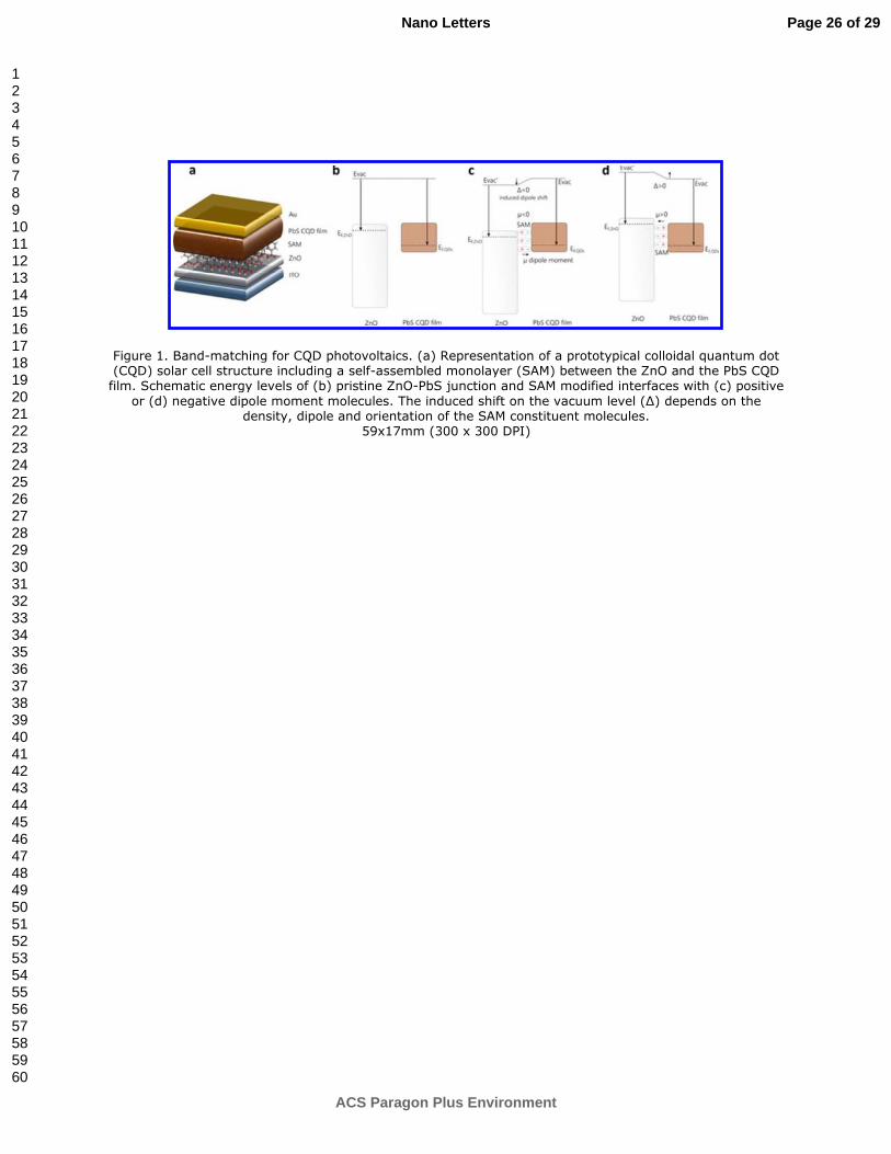
Figure 1. Band-matching for CQD photovoltaics. (a) Representation of a prototypical colloidal quantum dot (CQD) solar cell structure including a self-assembled monolayer (SAM) between the ZnO and the PbS CQD
film. Schematic energy levels of (b) pristine ZnO-PbS junction and SAM modified interfaces with (c) positive
or (d) negative dipole moment molecules. The induced shift on the vacuum level (∆) depends on the density, dipole and orientation of the SAM constituent molecules.
59x17mm (300 x 300 DPI)
Page 26 of 29
ACS Paragon Plus Environment
Nano Letters
123456789101112131415161718192021222324252627282930313233343536373839404142434445464748495051525354555657585960

1400x974mm (120 x 120 DPI)
Page 27 of 29
ACS Paragon Plus Environment
Nano Letters
123456789101112131415161718192021222324252627282930313233343536373839404142434445464748495051525354555657585960

Figure 3. Jointly tuning CQD exciton energy and induced dipole shift towards maximized photovoltaic performance. (a) In the absence of a dipole shift, maximum PCEs are predicted for CQDs with exciton energies in the 1.4-1.5 eV range. Further improvements are only within reach by introducing a positive
dipole shift. (b) Variation of open-circuit voltage as a function induced shift for 1.4 eV CQDs (dashed-horizontal line of panel a). (c) Simulated current-voltage characteristics under AM1.5G illumination for
induced dipole shifts of -0.15, 0eV, and +0.15eV. The complete set of photovoltaic figures of merit is shown in Figure S5.
62x19mm (300 x 300 DPI)
Page 28 of 29
ACS Paragon Plus Environment
Nano Letters
123456789101112131415161718192021222324252627282930313233343536373839404142434445464748495051525354555657585960
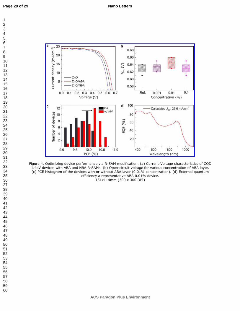
Figure 4. Optimizing device performance via R-SAM modification. (a) Current-Voltage characteristics of CQD 1.4eV devices with ABA and NBA R-SAMs. (b) Open-circuit voltage for various concentration of ABA layer. (c) PCE histogram of the devices with or without ABA layer (0.01% concentration). (d) External quantum
efficiency a representative ABA 0.01% device. 151x114mm (300 x 300 DPI)
Page 29 of 29
ACS Paragon Plus Environment
Nano Letters
123456789101112131415161718192021222324252627282930313233343536373839404142434445464748495051525354555657585960