very low-power, dual, current-feedback operational amplifier … sheets/texas... · 2009-09-09 ·...
TRANSCRIPT

www.ti.com
OPA2683
OPA2683
OPA2683
Copyright © 2002-2009, Texas Instruments Incorporated
Please be aware that an important notice concerning availability, standard warranty, and use in critical applications ofTexas Instruments semiconductor products and disclaimers thereto appears at the end of this data sheet.
SBOS244H – MAY 2002 – REVISED JULY 2009
Very Low-Power, Dual, Current-FeedbackOperational Amplifier
FEATURES REDUCED BANDWIDTH CHANGE VERSUS GAIN 150MHz BANDWIDTH G = +2 > 80MHz BANDWIDTH TO GAIN > +10 LOW DISTORTION: < –65dBc at 5MHz HIGH OUTPUT CURRENT: 110mA SINGLE-SUPPLY OPERATION: +5V to +12V DUAL-SUPPLY OPERATION: ±2.5V to ±6V LOW SUPPLY CURRENT: 1.9mA Total POWER SHUTDOWN VERSION: MSOP-10
V+
VO
V–
IERR
RG
RF
Z(S) IERR
+
Low-Power Amplifier
U.S. Patent No. 6,724,260
DESCRIPTIONThe OPA2683 provides a new level of performance for dual, verylow-power, wideband, current-feedback amplifiers. This CFBPLUS
amplifier is among the first to use an internally closed-loop inputbuffer stage that significantly enhances performance over earlierlow-power, current-feedback (CFB) amplifiers. This new archi-tecture provides many of the advantages of a more ideal CFBamplifier while retaining the benefits of very low-power operation.The closed-loop input stage buffer gives a very low and linearizedimpedance path at the inverting input to sense the feedback errorcurrent. This improved inverting input impedance gives excep-tional bandwidth retention to much higher gains and improvedharmonic distortion over earlier solutions limited by inverting inputlinearity. Beyond simple high gain applications, the OPA2683CFBPLUS amplifier can allow the gain setting element to be set withconsiderable freedom from amplifier bandwidth interaction. This
APPLICATIONS LOW-POWER BROADCAST VIDEO DRIVERS µPOWER ACTIVE FILTERS SHORT-LOOP ADSL CO DRIVERS MULTICHANNEL SUMMING AMPLIFIERS PROFESSIONAL CAMERAS DIFFERENTIAL ADC INPUT DRIVERS
flexibility allows frequency response peaking elements to beadded, multiple input inverting summing circuits to have greaterbandwidth, and low-power differential line drivers to meet thedemanding requirements of DSL.
The output capability for the OPA2683 also sets a new mark inperformance for very low-power, current-feedback amplifiers. De-livering a full ±4VPP swing on ±5V supplies, the OPA2683 also hasthe output current to support this swing into a 100Ω load. Thisminimal output headroom requirement is complemented by asimilar 1.2V input stage headroom, giving exceptional capability forsingle +5V operation.
The OPA2683’s low 1.9mA total supply current is precisely trimmedat +25°C. This trim, along with low shift over temperature and supplyvoltage, gives a very robust design over a wide range of operatingconditions. Further system power reduction is possible usingthe shutdown feature of the MSOP-10 package.
6
3
0
–3
–6
–9
–12
–15
–18
Frequency (Hz)
1 20010 100
NONINVERTING SMALL-SIGNALFREQUENCY RESPONSE
Nor
mal
ized
Gai
n (d
B)
G = 100
G = 50
G = 50
G = 10
G = 10 G = 1
G = 2
RF = 953Ω
PRODUCTION DATA information is current as of publication date.Products conform to specifications per the terms of Texas Instrumentsstandard warranty. Production processing does not necessarily includetesting of all parameters.
All trademarks are the property of their respective owners.
www.ti.com

OPA26832SBOS244Hwww.ti.com
Top View MSOP-10
ABSOLUTE MAXIMUM RATINGS(1)
Power Supply ............................................................................... ±6.5VDC
Internal Power Dissipation ...................................... See Thermal AnalysisDifferential Input Voltage .................................................................. ±1.2VInput Voltage Range ............................................................................ ±VS
Storage Temperature Range: ID, IDCN ......................... –65°C to +125°CLead Temperature (soldering, 10s) .............................................. +300°CJunction Temperature (TJ ) ........................................................... +150°CESD Rating: Human Body Model (HBM) ........................................ 2000V
Charged Device Model (CDM) .................................. 1000V
NOTE: (1) Stresses above those listed under Absolute Maximum Ratings maycause permanent damage to the device. Exposure to absolute maximumconditions for extended periods may affect device reliability.
SPECIFIEDPACKAGE TEMPERATURE PACKAGE ORDERING TRANSPORT
PRODUCT PACKAGE-LEAD DESIGNATOR RANGE MARKING NUMBER MEDIA, QUANTITY
OPA2683 SO-8 D –40°C to +85°C OPA2683 OPA2683ID Rails,100
" " " " " OPA2683IDR Tape and Reel, 2500
OPA2683 SOT23-8 DCN –40°C to +85°C B83 OPA2683IDCNT Tape and Reel, 250
" " " " " OPA2683IDCNR Tape and Reel, 3000
OPA2683 MSOP-10 DGS –40°C to +85°C BUI OPA2683IDGST Tape and Reel, 250
" " " " " OPA2683IDGSR Tape and Reel, 2500
PACKAGE/ORDERING INFORMATION(1)
ELECTROSTATICDISCHARGE SENSITIVITY
This integrated circuit can be damaged by ESD. Texas Instru-ments recommends that all integrated circuits be handled withappropriate precautions. Failure to observe proper handlingand installation procedures can cause damage.
ESD damage can range from subtle performance degradation tocomplete device failure. Precision integrated circuits may be moresusceptible to damage because very small parametric changescould cause the device not to meet its published specifications.
PIN CONFIGURATION
OPA2683 RELATED PRODUCTS
SINGLES DUALS TRIPLES QUADS FEATURES
OPA684 OPA2684 OPA3684 OPA4684 Low-Power CFBOPA691 OPA2691 OPA3691 — High Slew Rate CFBOPA695 OPA2695 OPA3695 — > 500MHz CFB
NOTE: (1) For the most current package and ordering information, see the Package Option Addendum at the end of this document, or see the TI web site at www.ti.com.
1
2
3
4
8
7
6
5
+VS
Out B
–In B
+In B
Out A
–In A
+In A
–VS
B83
Pin 1
1
2
3
4
8
7
6
5
+VS
Out B
–In B
+In B
Out A
–In A
+In A
–VS
Top View SO-8 Top View SOT23-8
1
2
3
4
5
10
9
8
7
6
–In A
Out A
+VS
Out B
–In B
+In A
DIS A
–VS
DIS B
+In B

OPA2683 3SBOS244H www.ti.com
AC PERFORMANCE (see Figure 1)Small-Signal Bandwidth (VO = 0.5VPP) G = +1, RF = 953kΩ 200 MHz typ C
G = +2, RF = 953Ω 150 124 121 117 MHz min BG = +5, RF = 953Ω 121 MHz typ CG = +10, RF = 953Ω 94 MHz typ BG = +20, RF = 953Ω 72 MHz typ C
Bandwidth for 0.1dB Gain Flatness G = +2, VO = 0.5VPP, RF = 953Ω 37 15 14 14 MHz min BPeaking at a Gain of +1 RF = 953Ω, VO = 0.5VPP 1.8 6.5 7.7 8.0 dB max BLarge-Signal Bandwidth G = +2, VO = 4VPP 63 MHz typ CSlew Rate G = –1, VO = 4V Step (see Figure 2) 540 450 450 430 V/µs min B
G = +2, VO = 4V Step 400 345 338 336 V/µs min BRise-and-Fall Time G = +2, VO = 0.5V Step 4.6 ns typ C
G = +2, VO = 4V Step 7.8 ns typ CHarmonic Distortion G = +2, f = 5MHz, VO = 2VPP2nd-Harmonic RL = 100Ω –63 –54 –54 –54 dBc max B
RL ≥ 1kΩ –71 –55 –55 –55 dBc max B3rd-Harmonic RL = 100Ω –67 –62 –62 –62 dBc max B
RL ≥ 1kΩ –77 –67 –66 –66 dBc max BInput Voltage Noise f > 1MHz 4.4 5.0 5.5 5.8 nV/√Hz max BNoninverting Input Current Noise f > 1MHz 5.1 5.8 6.4 6.7 pA/√Hz max BInverting Input Current Noise f > 1MHz 11.6 11.9 12.3 12.4 pA/√Hz max BDifferential Gain G = +2, NTSC, VO = 1.4VP, RL = 150Ω 0.13 % typ CDifferential Phase G = +2, NTSC, VO = 1.4VP, RL = 150Ω 0.06 deg typ CChannel-to-Channel Isolation f = 5MHz 70 dB typ C
DC PERFORMANCE(4)
Open-Loop Transimpedance Gain (ZOL) VO = 0V, RL = 1kΩ 700 300 270 250 kΩ min AInput Offset Voltage VCM = 0V ±1.5 ±3.5 ±4.1 ±4.3 mV max AAverage Offset Voltage Drift VCM = 0V ±12 ±12 µV/°C max BNoninverting Input Bias Current VCM = 0V ±2.0 ±4.5 ±5.1 ±5.3 µA max AAverage Noninverting Input Bias Current Drift VCM = 0V ±15 ±15 nA/°C max BInverting Input Bias Current VCM = 0V ±3.0 ±10 ±11 ±11.5 µA max AAverage Inverting Input Bias Current Drift VCM = 0V ±20 ±20 nA°/C max BINPUTCommon-Mode Input Range(5) (CMIR) ±3.75 ±3.65 ±3.65 ±3.60 V min ACommon-Mode Rejection Ratio (CMRR) VCM = 0V 60 53 52 52 dB min ANoninverting Input Impedance 50 2 kΩ || pF typ CInverting Input Resistance (RI) Open-Loop, DC 5.0 Ω typ COUTPUTVoltage Output Swing 1kΩ Load ±4.1 ±4.0 ±4.0 ±3.9 V min ACurrent Output, Sourcing VO = 0 150 120 115 110 mA min ACurrent Output, Sinking VO = 0 –110 –100 –95 –90 mA min AClosed-Loop Output Impedance G = +2, f = 100kHz 0.007 Ω typ CDISABLE (Disabled LOW) (MSOP-10 Only)Power-Down Supply Current (+VS) VDIS = 0, Both Channel –200 –300 –340 –360 µA max ADisable Time VIN = +1, See Figure 1 60 ms typ CEnable Time VIN = +1, See Figure 1 40 ns typ COff Isolation G = +2, 5MHz 70 dB typ COutput Capacitance in Disable 1.7 pF typ CTurn On Glitch G = +2, RL = 150Ω, VIN = 0 ±70 mV typ CTurn Off Glitch G = +2, RL = 150Ω, VIN = 0 ±20 mV typ CEnable Voltage 3.4 3.5 3.6 3.7 V min ADisable Voltage 1.8 1.7 1.6 1.5 V max AControl Pin Input Bias Current (DIS) VDIS = 0V, Each Channel 80 120 130 135 µA max A
POWER SUPPLYSpecified Operating Voltage ±5 V typ CMax Operating Voltage Range ±6 ±6 ±6 V max AMin Operating Voltage Range ±2 V typ CMax Quiescent Current VS = ±5V, Both Channels 1.88 2.06 2.08 2.10 mA max AMin Quiescent Current VS = ±5V, Both Channels 1.88 1.70 1.6 1.54 mA min APower-Supply Rejection Ratio (–PSRR) Input Referred 62 55 54 54 dB typ ATEMPERATURE RANGESpecification: D, DCN, DGS –40 to +85 °C typ CThermal Resistance, θJA Junction-to-Ambient
D SO-8 125 °C/W typ CDCN SOT23-8 150 °C/W typ CDGS MSOP-10 140 °C/W typ C
NOTES: (1) Junction temperature = ambient for +25°C tested specifications.(2) Junction temperature = ambient at low temperature limit: junction temperature = ambient +2°C at high temperature limit for over-temperature tested
specifications.(3) Test levels: (A) 100% tested at +25°C. Over-temperature limits by characterization and simulation. (B) Limits set by characterizationand simulation.
(C) Typical value only for information.(4) Current is considered positive out-of-node. VCM is the input common-mode voltage.(5) Tested < 3dB below minimum specified CMRR at ± CMIR limits.
OPA2683ID, IDCN, IDGS
TYP MIN/MAX OVER TEMPERATURE
0°C to –40°C to MIN/ TESTPARAMETER CONDITIONS +25°C +25°C(1) 70°C(2) +85°C(2) UNITS MAX LEVEL(3)
ELECTRICAL CHARACTERISTICS: VS = ±5VBoldface limits are tested at +25°C.RF = 953Ω, RL = 1kΩ, and G = +2 (see Figure 1 for AC performance only), unless otherwise noted.

OPA26834SBOS244Hwww.ti.com
AC PERFORMANCE (see Figure 3)Small-Signal Bandwidth (VO = 0.2VPP) G = +1, RF = 1.2kΩ 145 MHz typ
G = +2, RF = 1.2kΩ 119 96 92 90 MHz min BG = +5, RF = 1.2kΩ 95 MHz typ CG = +10, RF = 1.2kΩ 87 MHz typ CG = +20, RF = 1.2kΩ 60 MHz typ C
Bandwidth for 0.1dB Gain Flatness G = +2, VO < 0.5VPP, RF = 1.2kΩ 14 9 8 8 MHz min BPeaking at a Gain of +1 RF = 1.2kΩ, VO < 0.5VPP 1 6 8 8 dB max BLarge-Signal Bandwidth G = +2, VO = 2VPP 70 MHz typ CSlew Rate G = +2, VO = 2V Step 210 180 175 170 V/µs min BRise-and-Fall Time G = +2, VO = 0.5V Step 5.9 ns typ C
G = +2, VO = 2V Step 7.8 ns typ CHarmonic Distortion G = 2, f = 5MHz, VO = 2VPP2nd-Harmonic RL = 100Ω to VS/2 –60 –54 –53 –53 dBc max B
RL ≥ 1kΩ to VS/2 –66 –55 –55 –55 dBc max B3rd-Harmonic RL = 100Ω to VS/2 –59 –58 –58 –58 dBc max B
RL ≥ 1kΩ to VS/2 –74 –57 –56 –56 dBc max BInput Voltage Noise f > 1MHz 4.4 5.0 5.5 5.8 nV/√Hz max BNoninverting Input Current Noise f > 1MHz 5.1 5.8 6.4 6.7 pA/√Hz max BInverting Input Current Noise f > 1MHz 11.6 11.9 12.3 12.4 pA/√Hz max BDifferential Gain G = +2, NTSC, VO = 1.4VP, RL = 150Ω 0.24 % typ CDifferential Phase G = +2, NTSC, VO = 1.4VP, RL = 150Ω 0.19 deg typ CChannel-to-Channel Crosstalk f = 5MHz 70 dB type C
DC PERFORMANCE(4)
Open-Loop Transimpedance Gain (ZOL) VO = VS/2, RL = 1kΩ to VS/2 700 300 270 250 kΩ min AInput Offset Voltage VCM = VS/2 ±1.0 ±3.0 ±3.6 ±3.8 mV max AAverage Offset Voltage Drift VCM = VS/2 ±12 ±12 µV/°C max BNoninverting Input Bias Current VCM = VS/2 ±2 ±4.5 ±5.1 ±5.3 µA max AAverage Noninverting Input Bias Current Drift VCM = VS/2 ±12 ±12 nA/°C max BInverting Input Bias Current VCM = VS/2 ±3 ±8 ±8.7 ±8.9 µA max AAverage Inverting Input Bias Current Drift VCM = VS/2 ±15 ±15 nA°/C max B
INPUTLeast Positive Input Voltage(5) 1.1 1.25 1.29 1.34 V max AMost Positive Input Voltage(5) 3.9 3.75 3.73 3.67 V min ACommon-Mode Rejection Ratio (CMRR) VCM = VS/2 56 51 50 50 dB min ANoninverting Input Impedance 50 2 kΩ || pF typ CInverting Input Resistance (RI) Open-Loop, DC 5.6 Ω typ C
OUTPUTMost Positive Output Voltage RL = 1kΩ to VS/2 4.2 4.1 4.1 4.0 V min ALeast Positive Output Voltage RL = 1kΩ to VS/2 0.8 0.9 0.9 1.0 V max ACurrent Output, Sourcing VO = VS/2 80 65 63 58 mA min ACurrent Output, Sinking VO = VS/2 –70 –52 –50 –45 mA min AClosed-Loop Output Impedance G = +2, f = 100kHz 0.009 Ω typ C
DISABLE (Disabled LOW) (MSOP-10 Only)Power-Down Supply Current (+VS) VDIS = 0, Both Channels –200 µA typ COff Isolation G = +2, 5MHz 70 dB typ COutput Capacitance in Disable 1.7 pF typ CTurn On Glitch G = +2, RL = 150Ω, VIN = VS/2 ±70 mV typ CTurn Off Glitch G = +2, RL = 150Ω, VIN = VS/2 ±20 mV typ CEnable Voltage 3.4 3.5 3.6 3.7 V min ADisable Voltage 1.8 1.7 1.6 1.5 V max AControl Pin Input Bias Current (DIS) VDIS = 0V, Each Channel 80 120 130 135 µA max A
POWER SUPPLYSpecified Single-Supply Operating Voltage +5 V typ CMax Single-Supply Operating Voltage +12 +12 +12 V max AMin Single-Supply Operating Voltage +4 V typ CMax Quiescent Current VS = +5V, Both Channels 1.58 1.76 1.76 1.76 mA max AMin Quiescent Current VS = +5V, Both Channels 1.58 1.36 1.32 1.28 mA min APower-Supply Rejection Ratio (+PSRR) Input Referred 65 dB typ C
TEMPERATURE RANGESpecification: D, DCN, DGS –40 to +85 °C typ CThermal Resistance, θJA Junction-to-Ambient
D SO-8 125 °C/W typ CDCN SOT23-8 150 °C/W typ CDGS MSOP-10 140 °C/W typ C
NOTES: (1) Junction temperature = ambient for +25°C tested specifications.(2) Junction temperature = ambient at low temperature limit: junction temperature = ambient +2°C at high temperature limit for over-temperature tested
specifications.(3) Test levels: (A) 100% tested at +25°C. Over-temperature limits by characterization and simulation. (B) Limits set by characterization and simulation.
(C) Typical value only for information.(4) Current is considered positive out-of-node. VCM is the input common-mode voltage.(5) Tested < 3dB below minimum specified CMRR at ± CMIR limits.
ELECTRICAL CHARACTERISTICS: VS = +5VBoldface limits are tested at +25°C.RF = 1.2kΩ, RL = 1kΩ, and G = +2 (see Figure 3 for AC performance only), unless otherwise noted.
OPA2683ID, IDCN, IDGS
TYP MIN/MAX OVER TEMPERATURE
0°C to –40°C to MIN/ TESTPARAMETER CONDITIONS +25°C +25°C(1) 70°C(2) +85°C(2) UNITS MAX LEVEL(3)

OPA2683 5SBOS244H www.ti.com
TYPICAL CHARACTERISTICS: VS = ±5VTA = +25°C, G = +2, RF = 953Ω, and RL = 1kΩ, unless otherwise noted.
NONINVERTING PULSE RESPONSE
Time (10ns/div)
Out
put V
olta
ge (
200m
V/d
iv)
Out
put V
olta
ge (
800m
V/d
iv)
0.8
0.6
0.4
0.2
0
–0.2
–0.4
–0.6
–0.8
3.2
2.4
1.6
0.8
0
–0.8
–1.6
–2.4
–3.2
Large-Signal Right Scale
Small-Signal Left Scale
See Figure 1
G = +2
INVERTING PULSE RESPONSE
Time (10ns/div)
Out
put V
olta
ge (
200m
V/d
iv)
Out
put V
olta
ge (
800m
V/d
iv)
0.8
0.6
0.4
0.2
0
–0.2
–0.4
–0.6
–0.8
3.2
2.4
1.6
0.8
0
–0.8
–1.6
–2.4
–3.2
Large-Signal Right Scale
Small-Signal Left Scale
See Figure 2
G = –1
6
3
0
–3
–6
–9
–12
–15
–18
Frequency (MHz)
1 20010 100
NONINVERTING SMALL-SIGNALFREQUENCY RESPONSE
Nor
mal
ized
Gai
n (d
B)
G = 100
G = 50
G = 50
G = 10
G = 10 G = 1
G = 2
See Figure 1
6
3
0
–3
–6
–9
–12
–15
–18
Frequency (MHz)
1 20010 100
INVERTING SMALL-SIGNALFREQUENCY RESPONSE
Nor
mal
ized
Gai
n (d
B)
VO = 0.5VPPRF = 953Ω
See Figure 2 G = –20
G = –10
G = –1
G = –2
G = –5
9
6
3
0
–3
Frequency (MHz)
1 20010 100
NONINVERTING LARGE-SIGNALFREQUENCY RESPONSE
Nor
mal
ized
Gai
n (d
B)
RF = 953ΩG = +2
5VPP
1VPP
0.5VPP
2VPP
See Figure 1
3
0
–3
–6
–9
–12
Frequency (MHz)
1 20010 100
INVERTING LARGE-SIGNALFREQUENCY RESPONSE
Nor
mal
ized
Gai
n (d
B)
2VPP
0.5VPP
RF = 953ΩG = –2 1VPP
5VPP
See Figure 2
OPA26836SBOS244Hwww.ti.com
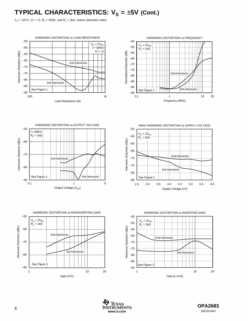
TYPICAL CHARACTERISTICS: VS = ±5V (Cont.)TA = +25°C, G = +2, RF = 953Ω, and RL = 1kΩ, unless otherwise noted.
–50
–60
–70
–80
–90
Gain (V/V)
1 10 20
HARMONIC DISTORTION vs NONINVERTING GAIN
Har
mon
ic D
isto
rtio
n (d
Bc)
2nd-Harmonic
3rd-Harmonic
See Figure 1
VO = 2VPPRL = 1kΩ
–50
–55
–60
–65
–70
–75
–80
–85
–90
Gain |(–V/V)|
1 2010
HARMONIC DISTORTION vs INVERTING GAIN
Har
mon
ic D
isto
rtio
n (d
Bc)
2nd-Harmonic
3rd-Harmonic
See Figure 2
VO = 2VPPRL = 1kΩ
–50
–55
–60
–65
–70
–75
–80
–85
–90
Load Resistance (Ω)
100 1k
HARMONIC DISTORTION vs LOAD RESISTANCE
Har
mon
ic D
isto
rtio
n (d
Bc)
VO = 2VPPf = 5MHz
G = +2
2nd-Harmonic
3rd-Harmonic
See Figure 1
–50
–55
–60
–65
–70
–75
–80
–85
–90
–95
Frequency (MHz)
0.1 201 10
HARMONIC DISTORTION vs FREQUENCY
Nor
mal
ized
Dis
tort
ion
(dB
)
2nd-Harmonic
VO = 2VPPRL = 1kΩ
3rd-HarmonicSee Figure 1
–50
–60
–70
–80
–90
Output Voltage (VPP)
0.1 51
HARMONIC DISTORTION vs OUTPUT VOLTAGE
Har
mon
ic D
isto
rtio
n (d
Bc)
f = 5MHzRL = 1kΩ
3rd-HarmonicSee Figure 1
2nd-Harmonic
–50
–55
–60
–65
–70
–75
–80
–85
Supply Voltage (±V)
2.5 3.0 3.5 4.0 4.5 6.05.0 5.5
5MHz HARMONIC DISTORTION vs SUPPLY VOLTAGEH
arm
onic
Dis
tort
ion
(dB
c)
VO = 2VPPRL = 1kΩ
2nd-Harmonic
See Figure 1
3rd-Harmonic

OPA2683 7SBOS244H www.ti.com
TYPICAL CHARACTERISTICS: VS = ±5V (Cont.)TA = +25°C, G = +2, RF = 953Ω, and RL = 1kΩ, unless otherwise noted.
100
10
1
Frequency (Hz)
100 10M1k 10k 100k 1M
INPUT VOLTAGE AND CURRENT NOISE DENSITY
Vol
tage
Noi
se (
nV/√
Hz)
Cur
rent
Noi
se (
pA/√
Hz)
Noninverting Current Noise5.2pA/√Hz
Voltage Noise4.4nV/√Hz
Inverting Current Noise11.6pA/√Hz
OPEN-LOOP TRANSIMPEDANCE GAIN AND PHASE
10k 100k 1M 10M 100M 1GFrequency (Hz)
Ope
n-Lo
op T
rans
impe
danc
e G
ain
(dB
Ω) 120
100
80
60
40
20
0
Ope
n-Lo
op P
hase
(°)
0
–30
–60
–90
–120
–150
–180
20log (ZOL)
∠ ZOL
–45
–50
–55
–60
–65
–70
–75
–80
–85
–90
VPP at 1kΩ Load (Each tone)
0.1 1 2
fO = 20MHz
fO = 10MHz
fO = 5MHz
fO = 1MHz
2-TONE, 3RD-ORDERINTERMODULATION DISTORTION
3rd-
Ord
er S
purio
us L
evel
(dB
c) +5V
–5V
50Ω
1kΩ
PI
PO
953Ω
953Ω
OPA2683
50
45
40
35
30
25
20
15
10
5
0
CLOAD (pF)
1 10 100
RS vs CLOAD
RS (
Ω)
0.5dB Peaking
CMRR AND PSRR vs FREQUENCY
100 1k 10k 100k 1M 10M 100MFrequency (Hz)
Com
mon
-Mod
e R
ejec
tion
Rat
io (
dB)
Pow
er-S
uppl
y R
ejec
tion
Rat
io (
dB)
70
60
50
40
30
20
10
0
CMRR
+PSRR
–PSRR
9
6
3
0
–3
–6
Frequency (Hz)
100k 1G1M 10M 100M
SMALL-SIGNAL BANDWIDTH vs CLOAD
Nor
mal
ized
Gai
n (d
Bc)
10pF
953Ω
1kΩ
OPA2683
RS VO
+5V
–5V
50Ω
CL
953Ω
VI
22pF
100pF
47pF
RS Adjusted to CLOAD

OPA26838SBOS244Hwww.ti.com
TYPICAL CHARACTERISTICS: VS = ±5V (Cont.)TA = +25°C, G = +2, RF = 953Ω, and RL = 1kΩ, unless otherwise noted.
TYPICAL DC DRIFT OVER TEMPERATURE
–50 –25 0 25 50 75 100 125
Ambient Temperature (°C)
Inpu
t Bia
s C
urre
nts
(µA
)an
d O
ffset
Vol
tage
(m
V)
4
3
2
1
0
–1
–2
–3
–4
Input Offset Voltage
Noninverting Input Bias Current
Inverting Input Bias Current
CLOSED-LOOP OUTPUT IMPEDANCE vs FREQUENCY
Frequency (Hz)
100k 1M1k 10k100 10M 100M
Out
put I
mpe
danc
e (Ω
)
100
10
1
0.01
0.001
953Ω ZO
953Ω
1/2OPA2683
0.20
0.15
0.10
0.05
0
Number of 150Ω Video Loads
1 42 3
COMPOSITE VIDEO DIFFERENTIAL GAIN/PHASE
Diff
eren
tial G
ain
(%)
Diff
eren
tial P
hase
(°)
Gain = +2NTSC, Positive Video
dG
dP
SETTLING TIME
0 10 20 30 40 50 60Time (ns)
% E
rror
to F
inal
Val
ue
0.05
0.04
0.03
0.02
0.01
0
–0.01
–0.02
–0.03
–0.04
–0.05
2V StepSee Figure 1
SUPPLY AND OUTPUT CURRENTvs TEMPERATURE
–25 0 25 50 75 100 125Ambient Temperature (°C)
Out
put C
urre
nt (
mA
)200
175
150
125
100
2.0
1.9
1.8
1.7
1.6
Sup
ply
Cur
rent
(m
A)
Sourcing Output Current
Sinking Output Current
Supply CurrentRight Scale
OUTPUT CURRENT AND VOLTAGE LIMITATIONS
–150 –100 –50 0 50 100 150IO (mA)
VO (
V)
5
4
3
2
1
0
–1
–2
–3
–4
–5
1W PowerLimit
R L =
100
Ω
R L = 50
Ω
R L =
500Ω
1W PowerLimitEach Channel

OPA2683 9SBOS244H www.ti.com
TYPICAL CHARACTERISTICS: VS = ±5V (Cont.)TA = +25°C, G = +2, RF = 953Ω, and RL = 1kΩ, unless otherwise noted.
NONINVERTING OVERDRIVE RECOVERY
Time (100ns/div)
Inpu
t Vol
tage
(0.
8V/d
iv)
Out
put V
olta
ge (
1.6V
/div
)
4.0
3.2
2.4
1.6
0.8
0
–0.8
–1.6
–2.4
–3.2
–4.0
8.0
6.4
4.8
3.2
1.6
0
–1.6
–3.2
–4.8
–6.4
–8.0
See Figure 1
Input VoltageLeft Scale
Output VoltageRight Scale
INPUT AND OUTPUT RANGE vs SUPPLY VOLTAGE
± Supply Voltage
± 4± 3± 2 ± 5 ± 6
Inpu
t and
Out
put V
olta
ge R
ange
6
5
4
3
2
1
0
–1
–2
–3
–4
–5
–6
InputVoltageRange
OutputVoltageRange
INVERTING OVERDRIVE RECOVERY
Time (100ns/div)
Inpu
t Vol
tage
(1.
6V/d
iv)
Inpu
t Vol
tage
(1.
6V/d
iv)
8.0
6.4
4.8
3.2
1.6
0
–1.6
–3.2
–4.8
–6.4
–8.0
8.0
6.4
4.8
3.2
1.6
0
–1.6
–3.2
–4.8
–6.4
–8.0
Input VoltageLeft Scale See Figure 2
Output VoltageRight Scale
0
–10
–20
–30
–40
–50
–60
–70
–80
–90
Frequency (Hz)
1M 10M 100M
CHANNEL-TO-CHANNEL CROSSTALK
Har
mon
ic D
isto
rtio
n (d
Bc)
Input Referred
6
5
4
3
2
1
0
Time (ms)
0 10010 20 4030 8070 906050
DISABLE TIME
VDIS
VOUT
VO
UT a
nd V
DIS
(V
)
VIN = 1VDCSee Figure 1
290
270
250
230
210
190
170
150
Ambient Temperature (°C)
50 25 0 25 50 12575 100
DISABLE SUPPLY CURRENT vs TEMPERATURE
Dis
able
Sup
ply
Cur
rent
(µA
)
Both Channels

OPA268310SBOS244Hwww.ti.com
TYPICAL CHARACTERISTICS: VS = ±5V (Cont.)TA = +25°C, G = +2, RF = 953Ω, and RL = 1kΩ, unless otherwise noted.
–40
–50
–60
–70
–80
–90
–100
Frequency (MHz)
0.1 1001 10
DISABLED FEEDTHRU
Fee
dthr
u (d
B)
G = +2VDIS = 0V
See Figure 1
Each Channel

OPA2683 11SBOS244H www.ti.com
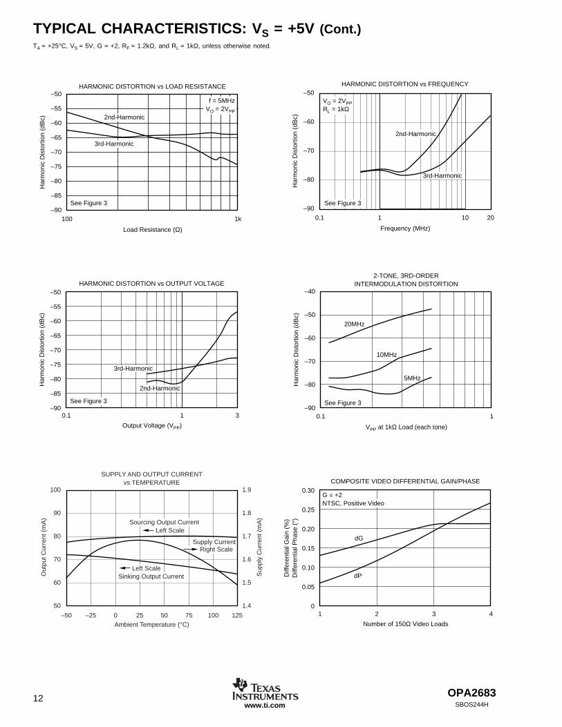
TYPICAL CHARACTERISTICS: VS = +5VTA = +25°C, VS = 5V, G = +2, RF = 1.2kΩ, and RL = 1kΩ, unless otherwise noted.
6
3
0
–3
–6
–9
–12
–15
–18
Frequency (MHz)
1 10010 200
NONINVERTING SMALL-SIGNALFREQUENCY RESPONSE
Nor
mal
ized
Gai
n (d
B)
G = 100
G = 50
G = 5
G = 10
G = 20
G = 2
G = 1
See Figure 3
6
3
0
–3
–6
–9
–12
–15
–18
Frequency (MHz)
1 10010 200
INVERTING SMALL-SIGNALFREQUENCY RESPONSE
Nor
mal
ized
Gai
n (d
B)
G = –10
G = –20
G = –2
G = –5
G = –1
See Figure 4
9
6
3
0
–3
Frequency (MHz)
1 10010 200
NONINVERTING LARGE-SIGNALFREQUENCY RESPONSE
Gai
n (d
B)
1VPP
2VPP
0.2VPP
0.5VPP
See Figure 3
3
0
–3
–6
–9
–12
Frequency (MHz)
1 20010 100
INVERTING LARGE-SIGNALFREQUENCY RESPONSE
Gai
n (d
B)
0.5VPP
2VPP
0.2VPP
1VPP
See Figure 4
NONINVERTING PULSE RESPONSE
Time (10ns/div)
Out
put V
olta
ge (
100m
V/d
iv)
Out
put V
olta
ge (
400m
V/d
iv)
0.4
0.3
0.2
0.1
0
–0.1
–0.2
–0.3
–0.4
1.6
1.2
0.8
0.4
0
–0.4
–0.8
–1.2
–1.6
Large-Signal Right Scale
Small-Signal Left Scale
See Figure 3
INVERTING PULSE RESPONSE
Time (10ns/div)
Out
put V
olta
ge (
100m
V/d
iv)
Out
put V
olta
ge (
400m
V/d
iv)
0.4
0.3
0.2
0.1
0
–0.1
–0.2
–0.3
–0.4
1.6
1.2
0.8
0.4
0
–0.4
–0.8
–1.2
–1.6
Large-Signal Right Scale
Small-Signal Left Scale
See Figure 4
OPA268312SBOS244Hwww.ti.com
TYPICAL CHARACTERISTICS: VS = +5V (Cont.)TA = +25°C, VS = 5V, G = +2, RF = 1.2kΩ, and RL = 1kΩ, unless otherwise noted.
–50
–55
–60
–65
–70
–75
–80
–85
–90
Load Resistance (Ω)
100 1k
HARMONIC DISTORTION vs LOAD RESISTANCE
Har
mon
ic D
isto
rtio
n (d
Bc) 2nd-Harmonic
3rd-Harmonic
See Figure 3
f = 5MHzVO = 2VPP
–50
–60
–70
–80
–90
Frequency (MHz)
0.1 101 20
HARMONIC DISTORTION vs FREQUENCY
Har
mon
ic D
isto
rtio
n (d
Bc)
2nd-Harmonic
3rd-Harmonic
VO = 2VPPRL = 1kΩ
See Figure 3
–50
–55
–60
–65
–70
–75
–80
–85
–90
Output Voltage (VPP)
0.1 31
HARMONIC DISTORTION vs OUTPUT VOLTAGE
Har
mon
ic D
isto
rtio
n (d
Bc)
3rd-Harmonic
2nd-Harmonic
See Figure 3
–40
–50
–60
–70
–80
–90
VPP at 1kΩ Load (each tone)
0.1
5MHz
See Figure 3
10MHz
20MHz
1
2-TONE, 3RD-ORDERINTERMODULATION DISTORTION
Har
mon
ic D
isto
rtio
n (d
Bc)
SUPPLY AND OUTPUT CURRENTvs TEMPERATURE
–50 –25 0 25 50 10075 125Ambient Temperature (°C)
Out
put C
urre
nt (
mA
)
100
90
80
70
60
50
1.9
1.8
1.7
1.6
1.5
1.4
Sup
ply
Cur
rent
(m
A)
Left ScaleSinking Output Current
Right ScaleSupply Current
Sourcing Output CurrentLeft Scale
0.30
0.25
0.20
0.15
0.10
0.05
0
Number of 150Ω Video Loads
1 42 3
COMPOSITE VIDEO DIFFERENTIAL GAIN/PHASE
Diff
eren
tial G
ain
(%)
Diff
eren
tial P
hase
(°)
dG
dP
G = +2NTSC, Positive Video
OPA2683 13SBOS244H www.ti.com
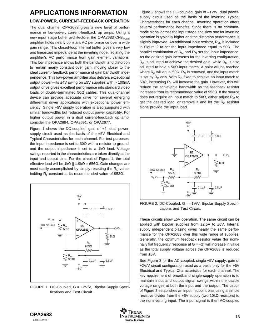
FIGURE 1. DC-Coupled, G = +2V/V, Bipolar Supply Speci-fications and Test Circuit.
FIGURE 2. DC-Coupled, G = –1V/V, Bipolar Supply Specifi-cations and Test Circuit.
APPLICATIONS INFORMATIONLOW-POWER, CURRENT-FEEDBACK OPERATION
The dual channel OPA2683 gives a new level of perfor-mance in low-power, current-feedback op amps. Using anew input stage buffer architecture, the OPA2683 CFBPLUS
amplifier holds nearly constant AC performance over a widegain range. This closed-loop internal buffer gives a very lowand linearized impedance at the inverting node, isolating theamplifier’s AC performance from gain element variations.This low impedance allows both the bandwidth and distortionto remain nearly constant over gain, moving closer to theideal current- feedback performance of gain bandwidth inde-pendence. This low-power amplifier also delivers exceptionaloutput power—its ±4V swing on ±5V supplies with > 100mAoutput drive gives excellent performance into standard videoloads or doubly-terminated 50Ω cables. This dual-channeldevice can provide adequate drive for several emergingdifferential driver applications with exceptional power effi-ciency. Single +5V supply operation is also supported withsimilar bandwidths but reduced output power capability. Forhigher output power in a dual current-feedback op amp,consider the OPA2684, OPA2691, or OPA2677.
Figure 1 shows the DC-coupled, gain of +2, dual power-supply circuit used as the basis of the ±5V Electrical andTypical Characteristics for each channel. For test purposes,the input impedance is set to 50Ω with a resistor to ground,and the output impedance is set to a 1kΩ load. Voltageswings reported in the characteristics are taken directly at theinput and output pins. For the circuit of Figure 1, the totaleffective load will be 1kΩ || 1.9kΩ = 656Ω. Gain changes aremost easily accomplished by simply resetting the RG value,holding RF constant at its recommended value of 953Ω.
Figure 2 shows the DC-coupled, gain of –1V/V, dual power-supply circuit used as the basis of the inverting TypicalCharacteristics for each channel. Inverting operation offersseveral performance benefits. Since there is no common-mode signal across the input stage, the slew rate for invertingoperation is typically higher and the distortion performance isslightly improved. An additional input resistor, RM, is includedin Figure 2 to set the input impedance equal to 50Ω. Theparallel combination of RM and RG set the input impedance.As the desired gain increases for the inverting configuration,RG is adjusted to achieve the desired gain, while RM is alsoadjusted to hold a 50Ω input match. A point will be reachedwhere RG will equal 50Ω, RM is removed, and the input matchis set by RG only. With RG fixed to achieve an input match to50Ω, increasing RF will increase the gain. However, this willreduce the achievable bandwidth as the feedback resistorincreases from its recommended value of 953Ω. If the sourcedoes not require an input match to 50Ω, either adjust RM toget the desired load, or remove it and let the RG resistoralone provide the input load.
These circuits show ±5V operation. The same circuit can beapplied with bipolar supplies from ±2.5V to ±6V. Internalsupply independent biasing gives nearly the same perfor-mance for the OPA2683 over this wide range of supplies.Generally, the optimum feedback resistor value (for nomi-nally flat frequency response at G = +2) will increase in valueas the total supply voltage across the OPA2683 is reducedfrom ±5V.
See Figure 3 for the AC-coupled, single +5V supply, gain of+2V/V circuit configuration used as a basis only for the +5VElectrical and Typical Characteristics for each channel. Thekey requirement of broadband single-supply operation is tomaintain input and output signal swings within the usablevoltage ranges at both the input and the output. The circuitof Figure 3 establishes an input midpoint bias using a simpleresistive divider from the +5V supply (two 10kΩ resistors) tothe noninverting input. The input signal is then AC-coupled
RF953Ω
1/2OPA2683
+5V
–5V
RM50Ω
RG953Ω
1kΩ
50Ω Source
VI
0.1µF 6.8µF
0.1µF 6.8µF
+
+
VO
RF953Ω
1/2OPA2683
+5V
–5V
RM52.3Ω
RG953Ω
50Ω Source
0.1µF 6.8µF
0.1µF 6.8µF
+
+
VI
1kΩ
VO

OPA268314SBOS244Hwww.ti.com
FIGURE 3. AC-Coupled, G = +2V/V, Single-Supply Specifi-cations and Test Circuit.
FIGURE 4. AC-Coupled, G = –1V/V, Single-Supply Specifi-cations and Test Circuit.
FIGURE 5. Noninverting Differential I/O Amplifier.
into this midpoint voltage bias. The input voltage can swingto within 1.25V of either supply pin, giving a 2.5VPP inputsignal range centered between the supply pins. The inputimpedance of Figure 3 is set to give a 50Ω input match. If thesource does not require a 50Ω match, remove this and drivedirectly into the blocking capacitor. The source will then seethe 5kΩ load of the biasing network. The gain resistor (RG)is AC-coupled, giving the circuit a DC gain of +1, which putsthe noninverting input DC bias voltage (2.5V) on the outputas well. The feedback resistor value has been adjusted fromthe bipolar ±5V supply condition to re-optimize for a flatfrequency response in +5V only, gain of +2, operation. On asingle +5V supply, the output voltage can swing to within0.9V of either supply pin while delivering more than 70mAoutput current, giving 3.2V output swing into 100Ω (8dBmmaximum at a matched 50Ω load). The circuit of Figure 3shows a blocking capacitor driving into a 1kΩ load. Alterna-tively, the blocking capacitor could be removed if the load istied to a supply midpoint or to ground if the DC currentrequired by the load is acceptable.
Figure 4 shows the AC-coupled, single +5V supply, gain of–1V/V circuit configuration used as a basis for the +5VTypical Characteristics for each channel. In this case, themidpoint DC bias on the noninverting input is also decoupledwith an additional 0.1µF decoupling capacitor. This reducesthe source impedance at higher frequencies for thenoninverting input bias current noise. This 2.5V bias on thenoninverting input pin appears on the inverting input pin and,since RG is DC blocked by the input capacitor, will alsoappear at the output pin. One advantage to inverting opera-tion is that since there is no signal swing across the inputstage, higher slew rates and operation to even lower supplyvoltages is possible. To retain a 1VPP output capability,operation down to 3V supply is allowed. At +3V supply, theinput stage is saturated, but for the inverting configuration of
a current-feedback amplifier, wideband operation is retainedeven under this condition.
The circuits of Figure 3 and 4 show single-supply operationat +5V. These same circuits may be used up to singlesupplies of +12V with minimal change in the performance ofthe OPA2683.
DIFFERENTIAL INTERFACE APPLICATIONS
Dual op amps are particularly suitable to differential input todifferential output applications. Typically, these fall into eitherAnalog-to-Digital Converter (ADC) input interfaces or linedriver applications. Two basic approaches to differential I/Oare noninverting or inverting configurations. Since the outputis differential, the signal polarity is somewhat meaningless—the noninverting and inverting terminology applies here towhere the input is brought into the OPA2683. Each has itsadvantages and disadvantages. Figure 5 shows a basicstarting point for noninverting differential I/O applications.
RF1.2kΩ
1/2OPA2683
+5V
50Ω Source
0.1µF 6.8µF+
10kΩ
10kΩRM50Ω
RG1.2kΩ
0.1µF
0.1µF
0.1µF
VI
1kΩ
VO
RF1.2kΩ
1/2OPA2683
+5V
50Ω Source
0.1µF
0.1µF
6.8µF+
RG1.2kΩ
10kΩ
10kΩ
0.1µF
VI
0.1µF
RM52.3Ω
1kΩ
VO
RF953Ω
RF953Ω
1/2OPA2683
+VCC
–VCC
RG VO
1/2OPA2683
VI

OPA2683 15SBOS244H www.ti.com
FIGURE 6. Inverting Differential I/O Amplifier.
FIGURE 7. Single to Differential Conversion.
This approach provides for a source termination impedancethat is independent of the signal gain. For instance, simpledifferential filters may be included in the signal path right upto the noninverting inputs without interacting with the gainsetting. The differential signal gain for the circuit of Figure 5 is:
AD = 1 + 2 • RF /RG
Since the OPA2683 is a CFBPLUS amplifier, its bandwidth isprincipally controlled with the feedback resistor value; seeFigure 5 for the recommended value of 953Ω. The differentialgain, however, may be adjusted with considerable freedomusing just the RG resistor. In fact, RG may be a reactivenetwork providing a very isolated shaping to the differentialfrequency response. Since the inverting inputs of the OPA2683are very low impedance closed-loop buffer outputs, the RG
element does not interact with the amplifier’s bandwidth;wide ranges of resistor values and/or filter elements may beinserted here with minimal amplifier bandwidth interaction.
Various combinations of single-supply or AC-coupled gaincan also be delivered using the basic circuit of Figure 5.Common-mode bias voltages on the two noninverting inputspass on to the output with a gain of 1 since an equal DCvoltage at each inverting node creates no current throughRG. This circuit does show a common-mode gain of 1 frominput to output. The source connection should either removethis common-mode signal if undesired (using an input trans-former can provide this function), or the common-modevoltage at the inputs can be used to set the output common-mode bias. If the low common-mode rejection of this circuitis a concern, the output interface may also be used to rejectthat common-mode. For instance, most modern differentialinput ADCs reject common-mode signals very well, while aline driver application through a transformer will also attenu-ate the common-mode signal through to the line.
Figure 6 shows a differential I/O stage configured as aninverting amplifier. In this case, the gain resistors (RG)become part of the input resistance for the source. Thisprovides a better noise performance than the noninvertingconfiguration but does limit the flexibility in setting the inputimpedance separately from the gain.
The two noninverting inputs provide an easy common-modecontrol input. This is particularly simple if the source isAC-coupled through either blocking caps or a transformer.In either case, the common-mode input voltages on the twononinverting inputs again have a gain of 1 to the output pins,giving particularly easy common-mode control for single-supply operation. The OPA2683 used in this configurationdoes constrain the feedback to the 953Ω region for bestfrequency response. With RF fixed, the input resistors may beadjusted to the desired gain but will also be changing theinput impedance as well. The high-frequency common-modegain for this circuit from input to output will be the same asfor the signal gain. Again, if the source might include anundesired common-mode signal, that signal could be re-jected at the input using blocking caps (for low frequency andDC common-mode) or a transformer coupling.
DC-COUPLED SINGLE TO DIFFERENTIAL CONVERSION
The previous differential output circuits were also set up toreceive a differential input. A simple way to provide a DC-coupled single to differential conversion using a dual op ampis shown in Figure 7. Here, the output of the first stage issimply inverted by the second to provide an inverting versionof a single amplifier design. This approach works well forlower frequencies but will start to depart from ideal differentialoutputs as the propagation delay and distortion of the invert-ing stage adds significantly to that present at the noninvertingoutput pin.
RF953Ω
RF953Ω
RG
RG
1/2OPA2683
+VCC
–VCC
VCM
VCM
VO
1/2OPA2683
VI
The circuit of Figure 7 is set up for a single-ended gain of 6to the output of the first amplifier, then an inverting gain of–1 through the second stage to provide a total differentialgain of 12. See Figure 8 for the 75MHz small-signal band-width delivered by the circuit of Figure 7. Large-signal distor-tion at 12VPP output at 1MHz into the 1kΩ differential load is≤ –76dBc.
953Ω12VPP Differential
953Ω
1/2OPA2683
+5V
–5V
953Ω
191Ω
1/2OPA2683
50Ω
1VPP
(1)

OPA268316SBOS244Hwww.ti.com
FIGURE 8. Small-Signal Bandwidth for Figure 7.
FIGURE 9. Low-Power, Differential I/O, 4th-Order Butterworth Active Filter.
DIFFERENTIAL ACTIVE FILTER
The OPA2683 can provide a very capable gain block for low-power active filters. The dual design lends itself very well todifferential active filters. Where the filter topology is lookingfor a simple gain function to implement the filter, thenoninverting configuration is preferred to isolate the filterelements from the gain elements in the design. Figure 9shows an example of a very low-power, 10MHz, 3rd-orderButterworth low-pass Sallen-Key filter. Often, these filters aredesigned at an amplifier gain of 1 to minimize amplifierbandwidth interaction with the desired filter shape. Since theOPA2683 shows minimal bandwidth change with gain, thisfeature would not be a constraint in this design. The example
of Figure 9 designs the filter for a differential gain of 5 usingthe OPA2683. The resistor values have been adjusted slightlyto account for the amplifier bandwidth effects.
While this circuit is bipolar, using ±5V supplies, it can easilybe adapted to single-supply operation. This is typically doneby providing a supply midpoint reference at the noninvertinginputs, then adding DC blocking caps at each input and inseries with the amplifier gain resistor, RG. This will add tworeal zeroes in the response, transforming the circuit into abandpass. Figure 10 shows the frequency response for thefilter of Figure 9.
FIGURE 10. Frequency Response for 10MHz, 3rd-OrderButterworth Low-Pass Filter.
24
21
18
15
12
9
6
3
Frequency (MHz)
1 20010 100
SINGLE TO DIFFERENTIAL CONVERSIONG
ain
(dB
)
VI VO
1/2OPA2683
1/2OPA2683183Ω47Ω
75pF22pF
100pF
183Ω47Ω
100pF
953Ω
20Ω
20Ω
953Ω
–5V
+5V
357Ω
357Ω
RG475Ω
14
11
8
5
2
–1
–4
Frequency (MHz)
1 2010
10MHz, 3RD-ORDER BUTTERWORTH LOW PASSFREQUENCY RESPONSE
Diff
eren
tial G
ain
(dB
)

OPA2683 17SBOS244H www.ti.com
SINGLE-SUPPLY, HIGH GAIN DIFFERENTIALADC DRIVER
Where a very low-power differential I/O interface to a moder-ate performance ADC is required, the circuit of Figure 11 maybe considered. The circuit builds on the inverting differentialI/O configuration of Figure 6 by adding the input transformerand the output low-pass filter. The input transformer providesa single-to-differential conversion where the input signal isstill very low power—it also provides a gain of 2 and removesany common-mode signal from the inputs. This single +5Vdesign sets a midpoint bias from the supply at each of thenoninverting inputs.
FIGURE 12. Frequency Response for 10MHz, 3rd-OrderButterworth Low-Pass Filter.
1/2OPA2683
1/2OPA2683
CL
0.1µF
800Ω
800Ω
+5V
RS
RS
200Ω
200Ω
500Ω (Optional)ADC
10kΩ
10kΩ
50ΩSource
15.3dBNoise Figure
Gain = 8V/V18.1dB
1:2
VCM
VCM
500Ω (Optional)
1/2OPA2683
681Ω 953Ω
75Ω78.7Ω
VOUT
75Ω Line
CH0
+5V
+5V
1/2OPA2683
681Ω 953Ω
75Ω78.7Ω
VOUT
75Ω Line
CH1
1/2OPA2683
681Ω 953Ω
75Ω78.7Ω
CH0
+5V
1/2OPA2683
681Ω 953Ω
75Ω78.7Ω
CH1
VDIS
U1
U2
Power-SupplyDecouplingNot Shown
FIGURE 11. Single-Supply Differential ADC Driver.
This circuit also includes optional 500Ω pull-down resistors atthe output. With a 2.5V DC common-mode operating point(set by VCM), this will add 5mA to ground in the output stage.This essentially powers up the NPN side of the output stagesignificantly reducing distortion. It is important for good 2nd-order distortion to connect the grounds of these two resistorsat the same point to minimize ground plane current for thedifferential output signal.
LOW-POWER MUX/LINE DRIVER
Using the shutdown feature, two OPA2683s can provide aneasy low-power way to select one of two possible sources formoderate-resolution monitors. Figure 12 shows a recom-mended circuit where each of the outputs are combined in away that provides a net gain of 1 to the matched 75Ω loadwith a 75Ω output impedance. This brings the two outputs foreach color together through a 78.7Ω resistor with a slightly> 2 gain provided by the amplifiers. When one channel isshutdown, the feedback network is still present, slightlyattenuating the signal and combining in parallel with the78.7Ω to give a 75Ω source impedance.
Since the OPA2683 does not disable quickly, this approachis not suitable for pixel-by-pixel multiplexing—however, itdoes provide an easy way to switch between two possibleRGB sources. The output swing provided by the activechannel will divide back through the inactive channel feed-back to appear at the inverting input of the OFF channel. Toretain good pulse fidelity, or low distortion, this divided downoutput signal at the inverting inputs of the OFF channels, plusthe OFF channel input signals, should not exceed 0.7VPP. Asthe signal across the buffers of the inactive channels ex-ceeds 0.7VPP, diodes across the inputs may begin to turn oncausing a nonlinear load to the active channel. This willdegrade signal linearity under those conditions.

OPA268318SBOS244Hwww.ti.com
The key elements of this current-feedback op amp model are:
α ⇒ Buffer gain from the noninverting input to the inverting input
RI ⇒ Buffer output impedance
iERR ⇒ Feedback error current signal
Z(s) ⇒ Frequency dependent open-loop transimpedancegain from iERR to VO
FIGURE 13. Current-Feedback Transfer Function AnalysisCircuit.
RF
VO
RG
RIZ(S) iERR
iERR
α
VI
ORDERING LITERATUREPRODUCT PACKAGE NUMBER NUMBER
OPA2683ID SO-8 DEM-OPA-SO-2A SBOU003OPA2683IDCN SOT23-8 DEM-OPA-SOT-2A SBOU001OPA2683IDGS MSOP-10 DEM-OPA-MSOP-2B SBOU040
TABLE I. Demonstration Fixtures by Package.
DESIGN-IN TOOLSDEMONSTRATION FIXTURES
Two printed circuit boards (PCBs) are available to assist inthe initial evaluation of circuit performance using the OPA2683in its two package options. Both of these are offered free ofcharge as unpopulated PCBs, delivered with a user’s guide.The summary information for these fixtures is shown inTable I.
The demonstration fixtures can be requested at the TexasInstruments web site (www.ti.com) through the OPA2683product folder.
MACROMODELS
Computer simulation of circuit performance using SPICE isoften useful when analyzing the performance of analogcircuits and systems. This is particularly true for higher speeddesigns where parasitic capacitance and inductance canhave a major effect on circuit performance. A SPICE modelfor the OPA683 is available in the product folder on the TIweb site (www.ti.com). This is the single channel model forthe OPA2683—simply use two of these to implement anOPA2683 simulation. These models do a good job of predict-ing small-signal AC and transient performance under a widevariety of operating conditions. However, they are less accu-rate in predicting the harmonic distortion or dG/dP character-istics. These models do not attempt to distinguish betweenthe package types in their small-signal AC performance.
OPERATING SUGGESTIONSSETTING RESISTOR VALUES TO OPTIMIZE BANDWIDTH
Any current-feedback op amp like the OPA2683 can holdhigh bandwidth over signal-gain settings with the properadjustment of the external resistor values. A low-power partlike the OPA2683 typically shows a larger change in band-width due to the significant contribution of the inverting inputimpedance to loop-gain changes as the signal gain is changed.Figure 13 shows a simplified analysis circuit for any current-feedback amplifier.

OPA2683 19SBOS244H www.ti.com
The buffer gain is typically very close to 1.00 and is normallyneglected from signal gain considerations. It will, however, setthe CMRR for a single op amp differential amplifier configura-tion. For the buffer gain α < 1.0, the CMRR = –20 • log(1 – α).The closed-loop input stage buffer used in the OPA2683 givesa buffer gain more closely approaching 1.00 and this shows upin a slightly higher CMRR than previous current-feedback opamps.
RI, the buffer output impedance, is a critical portion of thebandwidth control equation. The OPA2683 reduces thiselement to approximately 5.0Ω using the loop gain of theclosed-loop input buffer stage. This significant reduction inoutput impedance, on very low power, contributes signifi-cantly to extending the bandwidth at higher gains.
A current-feedback op amp senses an error current in theinverting node (as opposed to a differential input error volt-age for a voltage-feedback op amp) and passes this on tothe output through an internal frequency dependenttransimpedance gain. The Typical Characteristics show thisopen-loop transimpedance response. This is analogous tothe open-loop voltage gain curve for a voltage-feedback opamp. Developing the transfer function for the circuit of Figure13 gives Equation 2:
VV
RR
R RRR
Z
NGR R NG
Z
NGRR
O
I
F
G
F IF
G
S
F I
S
F
G
=+
++ +
=+ +
= +
αα
1
1
1 1
1
( )
( )
This is written in a loop-gain analysis format where the errorsarising from a non-infinite open-loop gain are shown in thedenominator. If Z(S) were infinite over all frequencies, thedenominator of Equation 2 would reduce to 1 and the idealdesired signal gain shown in the numerator would be achieved.The fraction in the denominator of Equation 2 determines thefrequency response. Equation 3 shows this as the loop-gainequation.
Z
R R NGLoop GainS
F I
( )
+=
If 20 • log(RF + NG • RI) were drawn on top of the open-looptransimpedance plot, the difference between the two wouldbe the loop gain at a given frequency. Eventually, Z(S) rolls offto equal the denominator of Equation 3, at which point theloop gain has reduced to 1 (and the curves have intersected).This point of equality is where the amplifier’s closed-loop
frequency response given by Equation 2 will start to roll off,and is exactly analogous to the frequency at which the noisegain equals the open-loop voltage gain for a voltage-feed-back op amp. The difference here is that the total impedancein the denominator of Equation 3 may be controlled some-what separately from the desired signal gain (or NG).
The OPA2683 is internally compensated to give a maximallyflat frequency response for RF = 953Ω at NG = 2 on ±5Vsupplies. That optimum value goes to 1.2kΩ on a single +5Vsupply. Normally, with a current-feedback amplifier, it ispossible to adjust the feedback resistor to hold this band-width up as the gain is increased. The CFBPLUS architecturehas reduced the contribution of the inverting input impedanceto provide exceptional bandwidth to higher gains withoutadjusting the feedback resistor value. The Typical Character-istics show the small-signal bandwidth over gain with a fixedfeedback resistor.
Putting a closed-loop buffer between the noninverting andinverting inputs does bring some added considerations. Sincethe voltage at the inverting output node is now the output ofa locally closed-loop buffer, parasitic external capacitance onthis node can cause frequency response peaking for thetransfer function from the noninverting input voltage to theinverting node voltage. While it is always important to keepthe inverting node capacitance low for any current-feedbackop amp, it is critically important for the OPA2683. Externallayout capacitance in excess of 2pF will start to peak thefrequency response. This peaking can be easily reduced bythen increasing the feedback resistor value—but it is prefer-able, from a noise and dynamic range standpoint, to keepthat capacitance low, allowing a close to nominal 953Ωfeedback resistor for flat frequency response. Very highparasitic capacitance values on the inverting node (> 5pF)can possibly cause input stage oscillation that cannot befiltered by a feedback element adjustment.
An added consideration is that at very high gains, 2nd-ordereffects in the inverting output impedance cause the overallresponse to peak up. If desired, it is possible to retain a flatfrequency response at higher gains by adjusting the feed-back resistor to higher values as the gain is increased. Sincethe exact value of feedback that will give a flat frequencyresponse at high gains depends strongly in inverting andoutput node parasitic capacitance values, it is best to experi-ment in the specific board with increasing values until thedesired flatness (or pulse response shape) is obtained. Ingeneral, increasing RF (and then adjusting RG to the desiredgain) will move towards flattening the response, while de-creasing it will extend the bandwidth at the cost of somepeaking. The OPA683 data sheet gives an example of thisoptimization of RF versus gain.
(2)
(3)

OPA268320SBOS244Hwww.ti.com
OUTPUT CURRENT AND VOLTAGE
The OPA2683 provides output voltage and current capabili-ties that can support the needs of driving doubly-terminated50Ω lines. If the 1kΩ load of Figure 1 is changed to a 100Ωload, the total load is the parallel combination of the 100Ωload, and the 1.9kΩ total feedback network impedance. This95Ω load will require no more than 42mA output current tosupport the ±4.0V minimum output voltage swing specifiedfor 1kΩ loads. This is well below the specified minimum+120/–90mA specifications over the full temperature range.
The specifications described above, though familiar in theindustry, consider voltage and current limits separately. Inmany applications, it is the voltage • current, or V-I product,which is more relevant to circuit operation. Refer to theOutput Voltage and Current Limitations plot in the TypicalCharacteristics. The X- and Y-axes of this graph show thezero-voltage output current limit and the zero-current outputvoltage limit, respectively. The four quadrants give a moredetailed view of the OPA2683’s output drive capabilities.Superimposing resistor load lines onto the plot shows theavailable output voltage and current for specific loads.
The minimum specified output voltage and current overtemperature are set by worst-case simulations at the coldtemperature extreme. Only at cold startup will the outputcurrent and voltage decrease to the numbers shown in theelectrical characteristic tables. As the output transistors de-liver power, their junction temperatures will increase, de-creasing their VBEs (increasing the available output voltageswing) and increasing their current gains (increasing theavailable output current). In steady-state operation, the avail-able output voltage and current will always be greater thanthat shown in the over-temperature specifications since theoutput stage junction temperatures will be higher than theminimum specified operating ambient.
To maintain maximum output stage linearity, no output short-circuit protection is provided. This will not normally be aproblem, since most applications include a series matchingresistor at the output that will limit the internal power dissipa-tion if the output side of this resistor is shorted to ground.However, shorting the output pin directly to the adjacentpositive power-supply pin can destroy the amplifier. If addi-tional short-circuit protection is required, consider a smallseries resistor in the power-supply leads. This resistor will,under heavy output loads, reduce the available output volt-age swing. A 5Ω series resistor in each power-supply leadwill limit the internal power dissipation to less than 1W for anoutput short-circuit, while decreasing the available outputvoltage swing only 0.25V for up to 50mA desired loadcurrents. Always place the 0.1µF power-supply decouplingcapacitors after these supply current limiting resistors directlyon the supply pins.
DRIVING CAPACITIVE LOADS
One of the most demanding and yet very common loadconditions for an op amp is capacitive loading. Often, thecapacitive load is the input of an ADC, including additionalexternal capacitance which may be recommended to im-prove ADC linearity. A high-speed, high open-loop gainamplifier like the OPA2683 can be very susceptible to de-creased stability and closed-loop response peaking when acapacitive load is placed directly on the output pin. When theamplifier’s open-loop output resistance is considered, thiscapacitive load introduces an additional pole in the signalpath that can decrease the phase margin. Several externalsolutions to this problem have been suggested. When theprimary considerations are frequency response flatness, pulseresponse fidelity, and/or distortion, the simplest and mosteffective solution is to isolate the capacitive load from thefeedback loop by inserting a series isolation resistor betweenthe amplifier output and the capacitive load. This does noteliminate the pole from the loop response, but rather shifts itand adds a zero at a higher frequency. The additional zeroacts to cancel the phase lag from the capacitive load pole,thus increasing the phase margin and improving stability.
The Typical Characteristics show the recommended RS vsCLOAD and the resulting frequency response at the load. The1kΩ resistor shown in parallel with the load capacitor is ameasurement path and may be omitted. The required seriesresistor value may be reduced by increasing the feedbackresistor value from its nominal recommended value. This willincrease the phase margin for the loop gain, allowing a lowerseries resistor to be effective in reducing the peaking due tocapacitive load. SPICE simulation can be effectively used tooptimize this approach. Parasitic capacitive loads greaterthan 5pF can begin to degrade the performance of theOPA2683. Long PC board traces, unmatched cables, andconnections to multiple devices can easily cause this valueto be exceeded. Always consider this effect carefully, andadd the recommended series resistor as close as possible tothe OPA2683 output pin (see Board Layout Guidelines).

OPA2683 21SBOS244H www.ti.com
DISTORTION PERFORMANCE
The OPA2683 provides very low distortion in a low-powerpart. The CFBPLUS architecture also gives two significantareas of distortion improvement. First, in operating regionswhere the 2nd-harmonic distortion due to output stagenonlinearities is very low (frequencies < 1MHz, low outputswings into light loads) the linearization at the inverting nodeprovided by the CFBPLUS design gives 2nd-harmonic distor-tions that extend into the –90dBc region. Previous current-feedback amplifiers have been limited to approximately–85dBc due to the nonlinearities at the inverting input. Thesecond area of distortion improvement comes in a distortionperformance that is largely gain independent. To the extentthat the distortion at a specific output power is output stagedependent, 3rd-harmonics particularly, and to a lesser ex-tend 2nd-harmonic distortion, remains constant as the gainincreases. This is due to the constant loop gain versus signalgain provided by the CFBPLUS design. As shown in theTypical Characteristics, while the 3rd-harmonic is constantwith gain, the 2nd-harmonic degrades at higher gains. Thisis largely due to board parasitic issues. Slightly imbalancedload return currents will couple into the gain resistor to causea portion of the 2nd-harmonic distortion. At high gains, thisimbalance has more gain to the output giving increased2nd-harmonic distortion.
Relative to alternative amplifiers with < 2mA supply current,the OPA2683 holds much lower distortion at higher frequen-cies (> 5MHz) and to higher gains. Generally, until thefundamental signal reaches very high frequency or powerlevels, the 2nd-harmonic will dominate the distortion with alower 3rd-harmonic component. Focusing then on the 2nd-harmonic, increasing the load impedance improves distortiondirectly. Remember that the total load includes the feedbacknetwork—in the noninverting configuration (see Figure 1) thisis the sum of RF + RG, while in the inverting configuration itis just RF. Also, providing an additional supply decouplingcapacitor (0.1µF) between the supply pins (for bipolar opera-tion) improves the 2nd-order distortion slightly (3dB to 6dB).
In most op amps, increasing the output voltage swing in-creases harmonic distortion directly. A low-power part likethe OPA2683 includes quiescent boost circuits to provide thefull-power bandwidth shown in the Typical Characteristics.These act to increase the bias in a very linear fashion onlywhen high slew rate or output power are required. This alsoacts to actually reduce the distortion slightly at higher outputpower levels. The Typical Characteristics show the 2nd-harmonic holding constant from 500mVPP to 5VPP outputswhile the 3rd-harmonics actually decrease with increasingoutput power.
The OPA2683 has an extremely low 3rd-order harmonicdistortion, particularly for light loads and at lower frequen-cies. This also gives low 2-tone, 3rd-order intermodulationdistortion as shown in the Typical Characteristics. Since theOPA2683 includes internal power boost circuits to retaingood full-power performance at high frequencies and out-puts, it does not show a classical 2-tone, 3rd-order inter-modulation intercept characteristic. Instead, it holds relativelylow and constant 3rd-order intermodulation spurious levelsover power. The Typical Characteristics show this spuriouslevel as a dBc below the carrier at fixed center frequenciesswept over single-tone power at a matched 50Ω load. Thesespurious levels drop significantly (> 12dB) for lighter loadsthan the 100Ω used in that plot. Converter inputs, for in-stance, will see ≤ 82dBc 3rd-order spurious to 10MHz for full-scale inputs. For even lower 3rd-order intermodulation distor-tion to much higher frequencies, consider the OPA2691.
NOISE PERFORMANCE
Wideband current-feedback op amps generally have a higheroutput noise than comparable voltage-feedback op amps.The OPA2683 offers an excellent balance between voltageand current noise terms to achieve low output noise in a low-power amplifier. The inverting current noise (11.6pA/√Hz) islower than most other current-feedback op amps while theinput voltage noise (4.4nV/√Hz) is lower than any unity-gainstable, comparable slew rate, < 5mA/ch voltage-feedback opamp. This low input voltage noise was achieved at the priceof higher noninverting input current noise (5.1pA/√Hz). Aslong as the AC source impedance looking out of thenoninverting node is less than 200Ω, this current noise willnot contribute significantly to the total output noise. The opamp input voltage noise and the two input current noiseterms combine to give low output noise under a wide varietyof operating conditions. Figure 14 shows the op amp noiseanalysis model with all the noise terms included. In thismodel, all noise terms are taken to be noise voltage orcurrent density terms in either nV/√Hz or pA/√Hz.
FIGURE 14. Op Amp Noise Analysis Model.
4kTRG
RG
RF
RS
1/2OPA2683
IBI
EO
IBN
4kT = 1.6E –20Jat 290°K
ERS
ENI
√4kTRS
√4kTRF

OPA268322SBOS244Hwww.ti.com
The total output spot noise voltage can be computed as thesquare root of the sum of all squared output noise voltagecontributors. Equation 4 shows the general form for theoutput noise voltage using the terms presented in Figure 14.
(4)
E E I R kTR NG I R kTR NGO NI BN S S BI F F= + ( ) +
+ ( ) +2 2 2 2
4 4
Dividing this expression by the noise gain (NG = (1 + RF/RG))will give the equivalent input referred spot noise voltage atthe noninverting input, as shown in Equation 5.
(5)
E E I R kTRI RNG
kTRNGN NI BN S S
BI F F= + ( ) + +
+2 22
44
Evaluating these two equations for the OPA2683 circuit andcomponent values (see Figure 1) will give a total output spotnoise voltage of 15.2nV/√Hz and a total equivalent input spotnoise voltage of 7.6nV/√Hz. This total input referred spotnoise voltage is higher than the 4.4nV/√Hz specification forthe op amp voltage noise alone. This reflects the noiseadded to the output by the inverting current noise times thefeedback resistor. As the gain is increased, this fixed outputnoise power term contributes less to the total output noiseand the total input referred voltage noise given by Equation 5will approach just the 4.4nV/√Hz of the op amp itself. Forexample, going to a gain of +20 in the circuit of Figure 1,adjusting only the gain resistor to 50Ω, will give a total inputreferred noise of 4.6nV/√Hz. A more complete description ofop amp noise analysis can be found in TI application noteAB-103, Noise Analysis for High-Speed Op Amps (SBOA066),located at www.ti.com.
DC ACCURACY AND OFFSET CONTROL
A current-feedback op amp like the OPA2683 providesexceptional bandwidth in high gains, giving fast pulse settlingbut only moderate DC accuracy. The Electrical Characteris-tics show an input offset voltage comparable to high slewrate voltage-feedback amplifiers. The two input bias currents,however, are somewhat higher and are unmatched. Whereasbias current cancellation techniques are very effective withmost voltage-feedback op amps, they do not generally re-duce the output DC offset for wideband current-feedback opamps. Since the two input bias currents are unrelated in bothmagnitude and polarity, matching the source impedancelooking out of each input to reduce their error contribution tothe output is ineffective. Evaluating the configuration ofFigure 1, using worst-case +25°C input offset voltage and thetwo input bias currents, gives a worst-case output offsetrange equal to:
±(NG • VOS) + (IBN • RS /2 • NG) ± (IBI • RF)
where NG = noninverting signal gain
= ±(2 • 3.5mV) ± (4.5µA • 25Ω • 2) ± (953Ω • 10mA)
= ±7.0mV + 0.23mV ± 9.5mV
= ±16.73mV
While the last term, the inverting bias current error, isdominant in this low-gain circuit, the input offset voltage willbecome the dominant DC error term as the gain exceeds5V/V. Where improved DC precision is required in a high-speed amplifier, consider the OPA656 single and OPA2822dual voltage-feedback amplifiers.
DISABLE OPERATION
The OPA2683 provides an optional disable feature that maybe used to reduce system power when channel operation isnot required. If the VDIS control pin is left unconnected, theOPA2683 will operate normally. To disable, the control pinmust be asserted LOW. Figure 14 shows a simplified internalcircuit for the disable control feature.
25kΩ 250kΩ
40kΩ
ISControl –VS
+VS
VDIS
Q1
FIGURE 14. Simplified Disable Control Circuit.
In normal operation, base current to Q1 is provided throughthe 250kΩ resistor while the emitter current through the 40kΩresistor sets up a voltage drop that is inadequate to turn onthe two diodes in Q1’s emitter. As VDIS is pulled LOW,additional current is pulled through the 40kΩ resistor eventu-ally turning on these two diodes (≈ 33µA). At this point, anyfurther current pulled out of VDIS goes through those diodesholding the emitter-base voltage of Q1 at approximately 0V.This shuts off the collector current out of Q1, turning theamplifier off. The supply current in the disable mode are onlythose required to operate the circuit of Figure 14.
When disabled, the output and input nodes go to a highimpedance state. If the OPA2683 is operating in a gain of +1(with a 1.2kΩ feedback resistor still required for stability), thiswill show a very high impedance (1.7pF || 1MΩ) at the outputand exceptional signal isolation. If operating at a gain greaterthan +1, the total feedback network resistance (RF + RG) willappear as the impedance looking back into the output, butthe circuit will still show very high forward and reverseisolation. If configured as an inverting amplifier, the input andoutput will be connected through the feedback networkresistance (RF + RG) giving relatively poor input to outputisolation.
OPA2683 23SBOS244H www.ti.com
The OPA2683 provides very high power gain on low quies-cent current levels. When disabled, internal high impedancenodes discharge slowly which, with the exceptional powergain provided, give a self powering characteristic that leadsto a slow turn off characteristic. Typical full turn off times torated 100µA disabled supply current are 60ms. Turn on timesare very fast—less than 40ns.
THERMAL ANALYSIS
The OPA2683 will not require external heatsinking for mostapplications. Maximum desired junction temperature will setthe maximum allowed internal power dissipation as de-scribed below. In no case should the maximum junctiontemperature be allowed to exceed 150°C.
Operating junction temperature (TJ) is given by TA + PD • θJA.The total internal power dissipation (PD) is the sum ofquiescent power (PDQ) and additional power dissipated in theoutput stage (PDL) to deliver load power. Quiescent power issimply the specified no-load supply current times the totalsupply voltage across the part. PDL will depend on therequired output signal and load but would, for a groundedresistive load, be at a maximum when the output is fixed ata voltage equal to 1/2 of either supply voltage (for equalbipolar supplies). Under this condition PDL = VS
2/(4 • RL)where RL includes feedback network loading.
Note that it is the power in the output stage and not into theload that determines internal power dissipation.
As an absolute worst-case example, compute the maximumTJ using an OPA2683IDCN (SOT23-8 package) in the circuitof Figure 1 operating at the maximum specified ambienttemperature of +85°C with both outputs driving a grounded100Ω load to 2.5VDC.
PD = 10V • 2.1mA + 2 • (52 /(4 • (100Ω || 1.9kΩ))) = 153mW
Maximum TJ = +85°C + (0.153W • 150°C/W) = 108°C
This maximum operating junction temperature is well belowmost system level targets. Most applications will be lowerthan this since an absolute worst-case output stage power inboth channels simultaneously was assumed in this calculation.
BOARD LAYOUT GUIDELINES
Achieving optimum performance with a high-frequency am-plifier like the OPA2683 requires careful attention to boardlayout parasitics and external component types. Recommen-dations that will optimize performance include:
a) Minimize parasitic capacitance to any AC ground forall of the signal I/O pins. Parasitic capacitance on theoutput and inverting input pins can cause instability; onthe noninverting input, it can react with the sourceimpedance to cause unintentional bandlimiting. To re-duce unwanted capacitance, a window around the sig-nal I/O pins should be opened in all of the ground andpower planes around those pins. Otherwise, ground andpower planes should be unbroken elsewhere on theboard.
b) Minimize the distance (< 0.25") from the power-sup-ply pins to high-frequency 0.1µF decoupling capaci-tors. At the device pins, the ground and power-planelayout should not be in close proximity to the signal I/Opins. Avoid narrow power and ground traces to minimizeinductance between the pins and the decoupling capaci-tors. The power-supply connections should always bedecoupled with these capacitors. An optional supplydecoupling capacitor (0.01µF) across the two powersupplies (for bipolar operation) will improve 2nd-har-monic distortion performance. Larger (2.2µF to 6.8µF)decoupling capacitors, effective at lower frequency,should also be used on the main supply pins. These maybe placed somewhat farther from the device and may beshared among several devices in the same area of thePC board.
c) Careful selection and placement of external compo-nents will preserve the high-frequency performanceof the OPA2683. Resistors should be a very low reac-tance type. Surface-mount resistors work best and allowa tighter overall layout. Metal film and carbon composi-tion axially-leaded resistors can also provide good high-frequency performance. Again, keep their leads andPCB trace length as short as possible. Never usewirewound type resistors in a high-frequency applica-tion. Since the output pin and inverting input pin are themost sensitive to parasitic capacitance, always positionthe feedback and series output resistor, if any, as closeas possible to the output pin. Other network compo-nents, such as noninverting input termination resistors,should also be placed close to the package. The fre-quency response is primarily determined by the feed-back resistor value as described previously. Increasingits value will reduce the peaking at higher gains, whiledecreasing it will give a more peaked frequency re-sponse at lower gains. The 800Ω feedback resistor usedin the Electrical Characteristics at a gain of +2 on ±5Vsupplies is a good starting point for design. Note that a953Ω feedback resistor, rather than a direct short, isrequired for the unity-gain follower application. A cur-rent-feedback op amp requires a feedback resistor evenin the unity-gain follower configuration to control stability.

OPA268324SBOS244Hwww.ti.com
FIGURE 15. Internal ESD Protection.
ExternalPin
+VCC
–VCC
InternalCircuitry
d) Connections to other wideband devices on the boardmay be made with short direct traces or through on-board transmission lines. For short connections, con-sider the trace and the input to the next device as alumped capacitive load. Relatively wide traces (50mils to100mils) should be used, preferably with ground andpower planes opened up around them. Estimate thetotal capacitive load and set RS from the plot of recom-mended Rs vs CLOAD. Low parasitic capacitive loads(< 5pF) may not need an RS since the OPA2683 isnominally compensated to operate with a 2pF parasiticload. If a long trace is required, and the 6dB signal lossintrinsic to a doubly-terminated transmission line is ac-ceptable, implement a matched impedance transmis-sion line using microstrip or stripline techniques (consultan ECL design handbook for microstrip and striplinelayout techniques). A 50Ω environment is normally notnecessary onboard, and in fact a higher impedanceenvironment will improve distortion, as shown in thedistortion versus load plots. With a characteristic boardtrace impedance defined based on board material andtrace dimensions, a matching series resistor into thetrace from the output of the OPA2683 is used, as well asa terminating shunt resistor at the input of the destina-tion device. Remember also that the terminating imped-ance will be the parallel combination of the shunt resistorand the input impedance of the destination device; thistotal effective impedance should be set to match thetrace impedance. The high output voltage and currentcapability of the OPA2683 allows multiple destinationdevices to be handled as separate transmission lines,each with their own series and shunt terminations. If the6dB attenuation of a doubly-terminated transmission lineis unacceptable, a long trace can be series-terminatedat the source end only. Treat the trace as a capacitiveload in this case and set the series resistor value asshown in the plot of Rs vs CLOAD. This will not preservesignal integrity as well as a doubly-terminated line. If theinput impedance of the destination device is low, therewill be some signal attenuation due to the voltage dividerformed by the series output into the terminating imped-ance.
e) Socketing a high-speed part like the OPA2683 is notrecommended. The additional lead length and pin-to-pin capacitance introduced by the socket can create anextremely troublesome parasitic network which can makeit almost impossible to achieve a smooth, stable fre-quency response. Best results are obtained by solderingthe OPA2683 onto the board.
INPUT AND ESD PROTECTION
The OPA2683 is built using a very high-speed complemen-tary bipolar process. The internal junction breakdown volt-ages are relatively low for these very small geometry de-vices. These breakdowns are reflected in the Absolute Maxi-mum Ratings table where an absolute maximum 13V acrossthe supply pins is reported. All device pins have limited ESDprotection using internal diodes to the power supplies, asshown in Figure 15.
These diodes provide moderate protection to input overdrivevoltages above the supplies as well. The protection diodescan typically support 30mA continuous current. Where highercurrents are possible (for example, in systems with ±15Vsupply parts driving into the OPA2683), current-limiting se-ries resistors should be added into the two inputs. Keepthese resistor values as low as possible since high valuesdegrade both noise performance and frequency response.

OPA2683 25SBOS244H www.ti.com
DATE REVISION PAGE SECTION DESCRIPTION
7/09 H 2 Package/Ordering Information Changed package markings for D (SO-8) and DGS (MSOP-10) packages.
7/08 G 2 Absolute Maximum Ratings Changed minimum storage temperature from −40°C to −65°C.
Revision History
NOTE: Page numbers for previous revisions may differ from page numbers in the current version.

PACKAGING INFORMATION
Orderable Device Status (1) PackageType
PackageDrawing
Pins PackageQty
Eco Plan (2) Lead/Ball Finish MSL Peak Temp (3)
OPA2683ID ACTIVE SOIC D 8 75 Green (RoHS &no Sb/Br)
CU NIPDAU Level-2-260C-1 YEAR
OPA2683IDCNR ACTIVE SOT-23 DCN 8 3000 Green (RoHS &no Sb/Br)
CU NIPDAU Level-2-260C-1 YEAR
OPA2683IDCNRG4 ACTIVE SOT-23 DCN 8 3000 Green (RoHS &no Sb/Br)
CU NIPDAU Level-2-260C-1 YEAR
OPA2683IDCNT ACTIVE SOT-23 DCN 8 250 Green (RoHS &no Sb/Br)
CU NIPDAU Level-2-260C-1 YEAR
OPA2683IDG4 ACTIVE SOIC D 8 75 Green (RoHS &no Sb/Br)
CU NIPDAU Level-2-260C-1 YEAR
OPA2683IDGSR ACTIVE MSOP DGS 10 2500 Green (RoHS &no Sb/Br)
CU NIPDAU Level-2-260C-1 YEAR
OPA2683IDGSRG4 ACTIVE MSOP DGS 10 2500 Green (RoHS &no Sb/Br)
CU NIPDAU Level-2-260C-1 YEAR
OPA2683IDGST ACTIVE MSOP DGS 10 250 Green (RoHS &no Sb/Br)
CU NIPDAU Level-2-260C-1 YEAR
OPA2683IDGSTG4 ACTIVE MSOP DGS 10 250 Green (RoHS &no Sb/Br)
CU NIPDAU Level-2-260C-1 YEAR
(1) The marketing status values are defined as follows:ACTIVE: Product device recommended for new designs.LIFEBUY: TI has announced that the device will be discontinued, and a lifetime-buy period is in effect.NRND: Not recommended for new designs. Device is in production to support existing customers, but TI does not recommend using this part ina new design.PREVIEW: Device has been announced but is not in production. Samples may or may not be available.OBSOLETE: TI has discontinued the production of the device.
(2) Eco Plan - The planned eco-friendly classification: Pb-Free (RoHS), Pb-Free (RoHS Exempt), or Green (RoHS & no Sb/Br) - please checkhttp://www.ti.com/productcontent for the latest availability information and additional product content details.TBD: The Pb-Free/Green conversion plan has not been defined.Pb-Free (RoHS): TI's terms "Lead-Free" or "Pb-Free" mean semiconductor products that are compatible with the current RoHS requirementsfor all 6 substances, including the requirement that lead not exceed 0.1% by weight in homogeneous materials. Where designed to be solderedat high temperatures, TI Pb-Free products are suitable for use in specified lead-free processes.Pb-Free (RoHS Exempt): This component has a RoHS exemption for either 1) lead-based flip-chip solder bumps used between the die andpackage, or 2) lead-based die adhesive used between the die and leadframe. The component is otherwise considered Pb-Free (RoHScompatible) as defined above.Green (RoHS & no Sb/Br): TI defines "Green" to mean Pb-Free (RoHS compatible), and free of Bromine (Br) and Antimony (Sb) based flameretardants (Br or Sb do not exceed 0.1% by weight in homogeneous material)
(3) MSL, Peak Temp. -- The Moisture Sensitivity Level rating according to the JEDEC industry standard classifications, and peak soldertemperature.
Important Information and Disclaimer:The information provided on this page represents TI's knowledge and belief as of the date that it isprovided. TI bases its knowledge and belief on information provided by third parties, and makes no representation or warranty as to theaccuracy of such information. Efforts are underway to better integrate information from third parties. TI has taken and continues to takereasonable steps to provide representative and accurate information but may not have conducted destructive testing or chemical analysis onincoming materials and chemicals. TI and TI suppliers consider certain information to be proprietary, and thus CAS numbers and other limitedinformation may not be available for release.
In no event shall TI's liability arising out of such information exceed the total purchase price of the TI part(s) at issue in this document sold by TIto Customer on an annual basis.
PACKAGE OPTION ADDENDUM
www.ti.com 26-Aug-2009
Addendum-Page 1

TAPE AND REEL INFORMATION
*All dimensions are nominal
Device PackageType
PackageDrawing
Pins SPQ ReelDiameter
(mm)
ReelWidth
W1 (mm)
A0(mm)
B0(mm)
K0(mm)
P1(mm)
W(mm)
Pin1Quadrant
OPA2683IDCNR SOT-23 DCN 8 3000 180.0 8.4 3.2 3.1 1.39 4.0 8.0 Q3
OPA2683IDCNT SOT-23 DCN 8 250 180.0 8.4 3.2 3.1 1.39 4.0 8.0 Q3
OPA2683IDGSR MSOP DGS 10 2500 330.0 12.4 5.3 3.4 1.4 8.0 12.0 Q1
OPA2683IDGST MSOP DGS 10 250 180.0 12.4 5.3 3.4 1.4 8.0 12.0 Q1
PACKAGE MATERIALS INFORMATION
www.ti.com 29-Jul-2009
Pack Materials-Page 1

*All dimensions are nominal
Device Package Type Package Drawing Pins SPQ Length (mm) Width (mm) Height (mm)
OPA2683IDCNR SOT-23 DCN 8 3000 190.5 212.7 31.8
OPA2683IDCNT SOT-23 DCN 8 250 190.5 212.7 31.8
OPA2683IDGSR MSOP DGS 10 2500 346.0 346.0 29.0
OPA2683IDGST MSOP DGS 10 250 190.5 212.7 31.8
PACKAGE MATERIALS INFORMATION
www.ti.com 29-Jul-2009
Pack Materials-Page 2


IMPORTANT NOTICETexas Instruments Incorporated and its subsidiaries (TI) reserve the right to make corrections, modifications, enhancements, improvements,and other changes to its products and services at any time and to discontinue any product or service without notice. Customers shouldobtain the latest relevant information before placing orders and should verify that such information is current and complete. All products aresold subject to TI’s terms and conditions of sale supplied at the time of order acknowledgment.TI warrants performance of its hardware products to the specifications applicable at the time of sale in accordance with TI’s standardwarranty. Testing and other quality control techniques are used to the extent TI deems necessary to support this warranty. Except wheremandated by government requirements, testing of all parameters of each product is not necessarily performed.TI assumes no liability for applications assistance or customer product design. Customers are responsible for their products andapplications using TI components. To minimize the risks associated with customer products and applications, customers should provideadequate design and operating safeguards.TI does not warrant or represent that any license, either express or implied, is granted under any TI patent right, copyright, mask work right,or other TI intellectual property right relating to any combination, machine, or process in which TI products or services are used. Informationpublished by TI regarding third-party products or services does not constitute a license from TI to use such products or services or awarranty or endorsement thereof. Use of such information may require a license from a third party under the patents or other intellectualproperty of the third party, or a license from TI under the patents or other intellectual property of TI.Reproduction of TI information in TI data books or data sheets is permissible only if reproduction is without alteration and is accompaniedby all associated warranties, conditions, limitations, and notices. Reproduction of this information with alteration is an unfair and deceptivebusiness practice. TI is not responsible or liable for such altered documentation. Information of third parties may be subject to additionalrestrictions.Resale of TI products or services with statements different from or beyond the parameters stated by TI for that product or service voids allexpress and any implied warranties for the associated TI product or service and is an unfair and deceptive business practice. TI is notresponsible or liable for any such statements.TI products are not authorized for use in safety-critical applications (such as life support) where a failure of the TI product would reasonablybe expected to cause severe personal injury or death, unless officers of the parties have executed an agreement specifically governingsuch use. Buyers represent that they have all necessary expertise in the safety and regulatory ramifications of their applications, andacknowledge and agree that they are solely responsible for all legal, regulatory and safety-related requirements concerning their productsand any use of TI products in such safety-critical applications, notwithstanding any applications-related information or support that may beprovided by TI. Further, Buyers must fully indemnify TI and its representatives against any damages arising out of the use of TI products insuch safety-critical applications.TI products are neither designed nor intended for use in military/aerospace applications or environments unless the TI products arespecifically designated by TI as military-grade or "enhanced plastic." Only products designated by TI as military-grade meet militaryspecifications. Buyers acknowledge and agree that any such use of TI products which TI has not designated as military-grade is solely atthe Buyer's risk, and that they are solely responsible for compliance with all legal and regulatory requirements in connection with such use.TI products are neither designed nor intended for use in automotive applications or environments unless the specific TI products aredesignated by TI as compliant with ISO/TS 16949 requirements. Buyers acknowledge and agree that, if they use any non-designatedproducts in automotive applications, TI will not be responsible for any failure to meet such requirements.Following are URLs where you can obtain information on other Texas Instruments products and application solutions:Products ApplicationsAmplifiers amplifier.ti.com Audio www.ti.com/audioData Converters dataconverter.ti.com Automotive www.ti.com/automotiveDLP® Products www.dlp.com Broadband www.ti.com/broadbandDSP dsp.ti.com Digital Control www.ti.com/digitalcontrolClocks and Timers www.ti.com/clocks Medical www.ti.com/medicalInterface interface.ti.com Military www.ti.com/militaryLogic logic.ti.com Optical Networking www.ti.com/opticalnetworkPower Mgmt power.ti.com Security www.ti.com/securityMicrocontrollers microcontroller.ti.com Telephony www.ti.com/telephonyRFID www.ti-rfid.com Video & Imaging www.ti.com/videoRF/IF and ZigBee® Solutions www.ti.com/lprf Wireless www.ti.com/wireless
Mailing Address: Texas Instruments, Post Office Box 655303, Dallas, Texas 75265Copyright © 2009, Texas Instruments Incorporated