university of california - microwave electronics...
TRANSCRIPT

UNIVERSITY of CALIFORNIASanta Barbara
Understanding material and process limits for high breakdown voltageAlGaN/GaN HEMTs
A dissertation submitted in partial satisfaction of the
requirements for the degree of
Doctor of Philosophy
in
Electrical and Computer Engineering
by
Yuvaraj Dora
Committee in charge:
Professor Umesh K. Mishra, ChairProfessor Robert A. YorkProfessor James S. SpeckDr. Sten HeikmanDr. Sriram Chandrasekaran
March 2006

The dissertation of Yuvaraj Dora is approved:
Chair
March 2006

Understanding material and process limits for high breakdown voltage
AlGaN/GaN HEMTs
Copyright 2006
by
Yuvaraj Dora
iii

Curriculum Vitæ
Yuvaraj Dora
EDUCATION
Bachelor of Technology in Electrical Engineering, Indian Institute of Technol-ogy, Chennai, India, March 2001.Bachelor’s thesis work,“Simulation of Resonant Tunneling Diodes by solvingPoisson and Schrodinger equations iteratively using Airy functions” done underthe guidance of Prof. Amitava DasGupta.
Doctor of Philosophy in Electrical and Computer Engineering, University ofCalifornia, Santa Barbara, March 2006 (expected).Doctoral thesis work,“Understanding material and process limits for high break-down voltage AlGaN/GaN HEMTs” done under the guidance of Prof. UmeshK. Mishra.
PUBLICATIONS
Y.Dora, A. Chakraborty, L. McCarthy, S. Keller, S. P. Denbaars, U. K. Mishra,“High breakdown voltage achieved in AlGaN/GaN HEMTs with trench gates”.submitted to IEEE Electron Device Letters.
Y.Dora, A. Chakraborty, S. Heikman, L. McCarthy, S. Keller, S. P. Denbaars,U. K. Mishra, “The effect of ohmic contacts on buffer leakage in GaN transis-tors”.submitted to IEEE Electron Device Letters.
Y. Dora, S. Han, D. Klenov, P. J. Hansen, K. Noc, U. K. Mishra, S. Stemmer,J. S. Speck, “ZrO2 gate dielectrics Produced by Ultraviolet Ozone Oxidation forGaN and AlGaN/GaN Transistors”, J. Vac. Sci. Technol. B, 24, pp 575, 2006.
Y. Dora, C. Suh, A. Chakraborty, S. Heikman, S. Chandrasekaran, V. Mehro-tra, U. K. Mishra, “Switching Characteristics of High Breakdown Voltage Al-GaN/GaN HEMTs”. Device Research Conference Digest, 2005, DRC 2005,
iv
63rd , vol.1, pp 191-192, June 20-22, 2005
Huili Xing, Y. Dora, A. Chini, S. Heikman, S. Keller, U. K. Mishra, “High break-down voltage AlGaN-GaN HEMTs achieved by multiple field plates,” IEEEElectron Device Letters, vol 25, no 4, pp 161-163, April 2004.
v

Abstract
Understanding material and process limits for high breakdown voltage
AlGaN/GaN HEMTs
by
Yuvaraj Dora
The breakdown voltage in AlGaN/GaN HEMTs is known to be triggered by
the gate leakage caused by the electric field crowding at the drain-side edge of
the gate. The effect of gate leakage on breakdown is mitigated by relieving
the peak electric field at the drain-side edge of the gate and by decreasing the
tunnelling probability with the use of gate dielectrics.
Multiple field-plates were used to split the single electric field peak into sev-
eral smaller peaks without compromising the frequency response too much. As
predicted by the device simulations, this increased the breakdown voltage of the
fabricated devices to 900 V with two field-plates. A technique yielding an inte-
grated field-plate self-aligned with the gate (trench gate technology) was devel-
vi
oped, in which the SiNx passivation was deposited before the gates, followed by
trenches being etched in the passivation and gate metal deposited in the trenches.
The profile of the etched trench wall could be controlled to shape the electric
field profile. Zirconium oxide produced by ozone oxidation shows promise as a
high-k gate dielectric for GaN. Increasing the Fe-doping in the buffer was shown
to reduce the buffer leakage and enhance the breakdown voltage. Furthermore,
alloyed ohmic contacts were identified as a source of buffer leakage.
Beyond 400 V, the parasitic breakdown of air was identified to be limiting
the device breakdown voltage. Devices made with trench gate technology, when
immersed in Fluoroinert liquid, had a breakdown voltage of more than a kilo-volt
(up to 1900 V was measured). Switching measurements were done on the diced
devices wirebonded to a compact switching test setup. A 5.5mm wide device
switched 2.4 A at 150 V with a turn-off time of less than 20 ns. The measured
switching speed is still limited by the gate drive speed. The on-resistance is
limited by the wirebond resistance and the increase in access resistance of the
device due to some amount of dispersion. This study has helped to give definitive
direction in developing AlGaN/GaN HEMTs for power applications.
vii

Contents
List of Figures xi
List of Tables xiv
1 Introduction 11.1 Figures of Merit for the switching transistors . . . . . . . . . . . 21.2 Advantages of GaN material system over other materials . . . . 41.3 Particular advantages of AlGaN/GaN HEMTs for power switching 61.4 Research background of high breakdown voltage AlGaN/GaN
HEMTs . . . . . . . . . . . . . . . . . . . . . . . . . . . . . . 71.5 Synopsis of this dissertation . . . . . . . . . . . . . . . . . . . 8References . . . . . . . . . . . . . . . . . . . . . . . . . . . . . . . . 11
2 Increasing Breakdown in AlGaN/GaN HEMTs using Mutiple FieldPlates 132.1 Introduction . . . . . . . . . . . . . . . . . . . . . . . . . . . . 132.2 The need for Field Plates . . . . . . . . . . . . . . . . . . . . . 142.3 Simulations . . . . . . . . . . . . . . . . . . . . . . . . . . . . 162.4 Device Fabrication and results . . . . . . . . . . . . . . . . . . 222.5 Discussion . . . . . . . . . . . . . . . . . . . . . . . . . . . . . 262.6 Summary . . . . . . . . . . . . . . . . . . . . . . . . . . . . . 29References . . . . . . . . . . . . . . . . . . . . . . . . . . . . . . . . 29
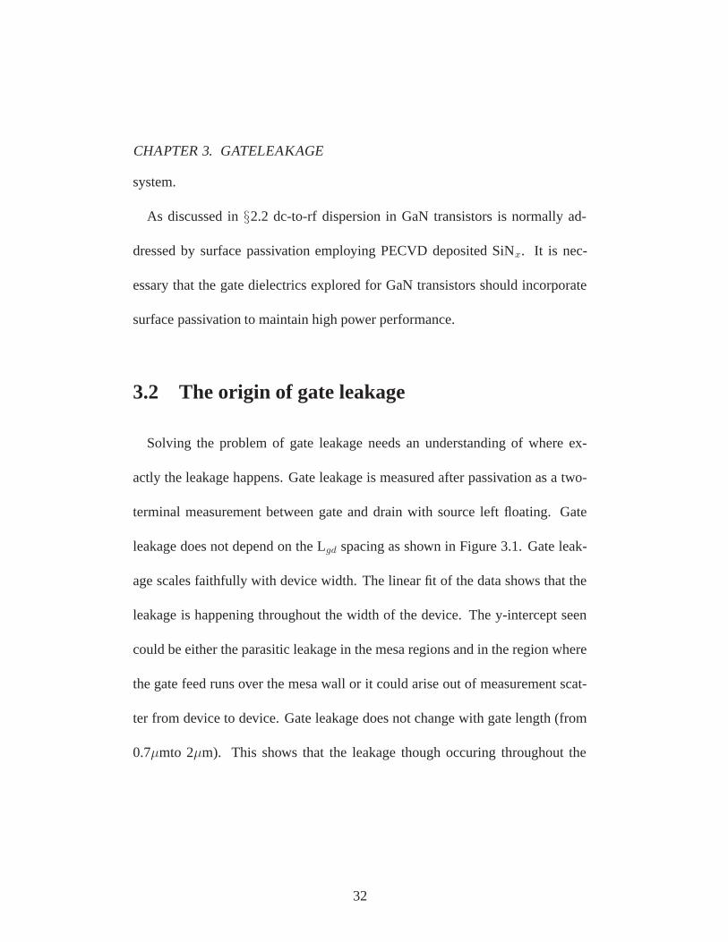
3 Gate Leakage in AlGaN/GaN HEMTs 313.1 Introduction . . . . . . . . . . . . . . . . . . . . . . . . . . . . 313.2 The origin of gate leakage . . . . . . . . . . . . . . . . . . . . 32
viii
3.3 Reducing gate leakage . . . . . . . . . . . . . . . . . . . . . . 363.3.1 Reducing gate leakage by using trench gates . . . . . . 363.3.2 Literature survey of reducing gate leakage in GaN de-
vices using dielectrics . . . . . . . . . . . . . . . . . . 383.3.3 Reducing gate leakage by using in-situ grown dielectrics 403.3.4 Reducing gate leakage by using ZrO2 dielectric . . . . . 42
3.4 Leakage from field-plates: . . . . . . . . . . . . . . . . . . . . 533.5 Summary . . . . . . . . . . . . . . . . . . . . . . . . . . . . . 56References . . . . . . . . . . . . . . . . . . . . . . . . . . . . . . . . 57
4 Buffer Leakage in GaN Transistors 604.1 Introduction . . . . . . . . . . . . . . . . . . . . . . . . . . . . 604.2 Test Structures . . . . . . . . . . . . . . . . . . . . . . . . . . 614.3 Effect of Fe-doping level on the buffer leakage . . . . . . . . . . 634.4 Effect of ohmic contacts on buffer leakage . . . . . . . . . . . . 65
4.4.1 Observation of differences in buffer leakage . . . . . . . 654.4.2 Interpretation of Electrical data . . . . . . . . . . . . . 694.4.3 Interpretation for Morphology . . . . . . . . . . . . . . 714.4.4 Ways to reduce the effect of ohmics on buffer leakage in
HEMTs . . . . . . . . . . . . . . . . . . . . . . . . . . 734.5 Conducting SiC substrate for GaN transistors . . . . . . . . . . 744.6 Summary . . . . . . . . . . . . . . . . . . . . . . . . . . . . . 78References . . . . . . . . . . . . . . . . . . . . . . . . . . . . . . . . 78
5 Kilo-Volt breakdown voltage devices and wide periphery devices 805.1 Introduction . . . . . . . . . . . . . . . . . . . . . . . . . . . . 805.2 Trench gate process : Self-aligned field-plates . . . . . . . . . . 81
5.2.1 Controlling the profile of the trench . . . . . . . . . . . 815.2.2 Controlling the field-plate extension . . . . . . . . . . . 835.2.3 The Effect of Source-side dispersion . . . . . . . . . . . 855.2.4 Frequency response of the trench-gates . . . . . . . . . 89
5.3 Kilo-Volt breakdown voltage devices . . . . . . . . . . . . . . . 915.3.1 Identifying the parasitic breakdown . . . . . . . . . . . 925.3.2 Kilo-Volt breakdown measurements . . . . . . . . . . . 95
5.4 What is limiting the breakdown voltage ? . . . . . . . . . . . . 96
ix

5.5 Wide periphery devices . . . . . . . . . . . . . . . . . . . . . . 1005.6 Summary . . . . . . . . . . . . . . . . . . . . . . . . . . . . . 103References . . . . . . . . . . . . . . . . . . . . . . . . . . . . . . . . 104
6 Switching measurements 1056.1 The need for switching measurements . . . . . . . . . . . . . . 1056.2 Switching setup schematic and waveforms . . . . . . . . . . . . 1086.3 The need for compact test setup . . . . . . . . . . . . . . . . . 1106.4 Measurements with a compact test setup . . . . . . . . . . . . . 1116.5 Issues with switching measurements . . . . . . . . . . . . . . . 116
6.5.1 Gate drive speed . . . . . . . . . . . . . . . . . . . . . 1166.5.2 High Von . . . . . . . . . . . . . . . . . . . . . . . . . 1186.5.3 Heat sinking the devices . . . . . . . . . . . . . . . . . 1206.5.4 Ongoing improvements with switching measurements . 122
6.6 Summary . . . . . . . . . . . . . . . . . . . . . . . . . . . . . 123References . . . . . . . . . . . . . . . . . . . . . . . . . . . . . . . . 123
7 Conclusions and future work 1257.1 Conclusions . . . . . . . . . . . . . . . . . . . . . . . . . . . . 1257.2 Future Work . . . . . . . . . . . . . . . . . . . . . . . . . . . . 127
A ATLAS code for simulating AlGaN/GaN HEMTs 129
B SiNx deposition conditions 134
C Specifics of Processing 135
x

List of Figures
1.1 Figure of merit: theoritical limits of material systems . . . . . . 51.2 Epitaxy and Device schematic of AlGaN/GaN HEMT . . . . . . 7
2.1 Schematic of the devices . . . . . . . . . . . . . . . . . . . . . 152.2 Simulated Potential contours . . . . . . . . . . . . . . . . . . . 172.3 Electric field profiles . . . . . . . . . . . . . . . . . . . . . . . 182.4 E-field profiles with applied voltage . . . . . . . . . . . . . . . 192.5 E-field profiles with thickness of dielectric beneath field-plates . 202.6 E-field profiles with lateral shift of field-plates . . . . . . . . . . 212.7 Epitaxial structure and Fabricated Device schematic . . . . . . . 222.8 Pulsed-IV before and after passivation . . . . . . . . . . . . . . 232.9 SEM cross-section of the fabricated device . . . . . . . . . . . . 242.10 High breakdown voltage achieved with two field-plates . . . . . 252.11 Breakdown voltage with processing steps . . . . . . . . . . . . 262.12 Small signal frequency response after three field-plates . . . . . 28
3.1 The dependence of Gate Leakage with Lgd and Wg . . . . . . . 333.2 Leakage is not through the SiNx layer . . . . . . . . . . . . . . 343.3 Gate Leakage in HEMTs grown on LEO GaN template . . . . . 353.4 Gate leakage reduction using trench-gate process . . . . . . . . 373.5 In-situ MOCVD dielectrics . . . . . . . . . . . . . . . . . . . . 413.6 Process flow for HEMTs with ZrO2 . . . . . . . . . . . . . . . 433.7 TEM characterization of ZrO2 film . . . . . . . . . . . . . . . . 453.8 Gate leakage reduction using zirconium oxide underneath the gate 473.9 Controlled experiment to show that the reduction is due to ZrO2 49
xi

3.10 Problems with integrating ZrO2 into the HEMT process flow. . . 503.11 An Approach to integrate ZrO2 into the HEMT process flow. . . 523.12 Leakage from fieldplate through passivation layer. . . . . . . . . 543.13 Leakage from fieldplate through different passivation layers. . . 55
4.1 Epitaxial structure of a HEMT and MESFET . . . . . . . . . . 624.2 Effect of Fe-doping level on buffer leakage . . . . . . . . . . . 644.3 Buffer Leakage test structures to study the effect of ohmic contacts 664.4 Optical microscope picture and AFM scan-section of the ohmic
regions after stripping the alloyed metals . . . . . . . . . . . . . 674.5 Morphology explains the difference in buffer leakage . . . . . . 684.6 Removal of spiky ohmics translates to higher device breakdown 744.7 Effect of Fe on buffers grown on n-SiC substrate . . . . . . . . 754.8 Pulsed-IV amd Power measurements in HEMTs grown on n-SiC
substrate . . . . . . . . . . . . . . . . . . . . . . . . . . . . . . 764.9 Removal of spiky ohmics gave reduced buffer leakage in HEMTs
on n-SiC substrate . . . . . . . . . . . . . . . . . . . . . . . . . 77
5.1 Profile of the etched trench . . . . . . . . . . . . . . . . . . . . 825.2 SEM picture of the trench-gate . . . . . . . . . . . . . . . . . . 845.3 Effect of source side dispersion . . . . . . . . . . . . . . . . . . 865.4 Explanation for IV-curves of devices with dispersion on drain-
side only and source-side only. . . . . . . . . . . . . . . . . . . 875.5 Small signal characteristics and pulsed-IV . . . . . . . . . . . . 905.6 Load-pull power measurements at 4GHz . . . . . . . . . . . . . 915.7 Effect of etched mesa wall on breakdown . . . . . . . . . . . . 925.8 Breakdown voltage of 1400 V measured . . . . . . . . . . . . . 955.9 Dependence of Breakdown voltage with Lgd spacing . . . . . . 965.10 Dependence of Breakdown voltage with Lsg spacing . . . . . . 995.11 Picture of a flip-chip bonded device . . . . . . . . . . . . . . . 101
6.1 Switching test setup and waveforms . . . . . . . . . . . . . . . 1076.2 The need for compact test setup . . . . . . . . . . . . . . . . . 1106.3 Compact switching test setup . . . . . . . . . . . . . . . . . . . 1116.4 Gate transition times . . . . . . . . . . . . . . . . . . . . . . . 112
xii

6.5 Switching measurements with high speed gate drive . . . . . . . 1136.6 High current turn-off characteristic . . . . . . . . . . . . . . . . 1146.7 Current and Voltage waveform crossover locus . . . . . . . . . 1166.8 The gate drive schematic . . . . . . . . . . . . . . . . . . . . . 1176.9 Effect of source side parasitic resistance on Von . . . . . . . . . 1206.10 High current switching . . . . . . . . . . . . . . . . . . . . . . 121
xiii

List of Tables
1.1 Physical properties of various semiconductors relevant to high-voltage applications . . . . . . . . . . . . . . . . . . . . . . . 6
xiv

Acknowledgements
I would like to thank my advisor Prof. Umesh Mishra for providing me an
oppurtunity to participate in the research in his group. It is my pleasure to have
worked in one of the leading groups for research in GaN devices. I also thank
Prof. Mishra for providing me the financial aid during my graduate school.
I would like to thank all my committee members for their guidance and feed-
back. I would like to thank Prof. Robert York for letting me use the microwave
lab facilities. I would like to thank Prof. James Speck and Prof. Susanne Stem-
mer for helping me with the work on zirconium oxide gate dielectrics and help-
ing me with the material characterization. I would like to thank Sten for guiding
me on the project and growing many samples in attempts to understand the buffer
leakage. I appreciate the amount of time he spent in growing samples for this
project. I would like to thank Sriram and Vivek for their help in doing the switch-
ing measurements. I am grateful for the time that Sriram spent on designing a
compact switching test setup and teaching me the concepts of gate drivers.
This project involved intensive use of the Nanofab facilities at UCSB. I thank
the efforts of the Nanofab engineers Bob, Brian, Don, Jack, Louis, Mike, Neil,
xv

Ning to keep the lab running smoothly. This work would not have been possible
if not for the expertise and the time commitment of the people in the MOCVD
lab. I would like to thank Arpan, Gia, Lee, Nick, Stacia, Sten and Prof. DenBaars
for their help. The data storage and analysis would not have been possible if not
for the help and guidance of Chris, Mike, Eric, Val, John, Guylene and Ken.
I would like to thank all the members of Mishra-York group for their contribu-
tion to maintain the high quality of the microwave lab. I thank Ajay, Ale, Arpan,
Carl, Chang-soo, Chris Sanabria, Chris Schaake, Dario, Felix, Hongtao, Huili,
Ilan, Jaehoon , Lal, Lee, Likun, Manhoi, Mike, Mishra, Nadia, Nick, Pete, Sid-
dharth, Srabanti, Stacia, Sten, Raj, Tomas, Val, Yenyun, Yipei and York for their
cooperation. I thank Dmitri, Pete, and Soo-yeon for their help in characterizing
the zirconia film, Hisashi and James for their help in wirebonding and Navin for
his help with the SEM. I would like to thank Jim-Ping, Mark for their help with
AFM and SEM. I would like to thank Prof. Evelyn Hu, Prof. Mark Sherwin,
Carey and Dario from whom I learnt various experimental techniques.
I would like to acknowledge the help that I received regarding paperwork from
Laura, Lee Baboolal, Lynn, Mike, Val and others. Finally, I would like to thank
all the friends, who made my stay here pleasant and educative .
xvi

Dedicated to
xvii

1Introduction
DURING the past few years, enormous progress has been made in the de-
velopment of Gallium Nitride (GaN) and its family of material alloys
for both electronics and opto-electronics applications. For electronics applica-
tions, a number of devices take advantage of both the high critical breakdown
field associated with the large bandgap of GaN as well as its high saturated elec-
tron velocities. These devices are intended to fulfill the growing demands for
high power at high frequency electronic components as well as for high voltage
power switches operating at higher frequencies. Improvements in AlGaN/GaN
high electron mobility transistors (HEMTs) [1] and heterojunction bipolar tran-
sistors (HBTs) [2] continue to be reported, and microwave GaN HEMTs have
been commercialized.
This dissertation will focus on the improvements in high breakdown voltage
1
CHAPTER 1. INTRODUCTION
AlGaN/GaN HEMTs with low Ron for power switching applications. The pri-
mary focus of the work was to improve the device design, to identify the param-
eters critical to the device breakdown and to develop the processing techniques
for the fabrication of devices with high breakdown voltage. The use of multiple
field-plates enabled high breakdown voltages without sacrificing the frequency
response too much. Several dielectric materials were also tried to be used as
gate dielectric to reduce the gate leakage in AlGaN/GaN HEMTs. The alloyed
ohmic contacts were identified as an additional source of buffer leakage. High
breakdown voltage measurement techniques were developed. Switching mea-
surements were done to characterize the large signal frequecy response of the
devices. As a whole, this work has also contributed to the overall understand-
ing of AlGaN/GaN HEMTs, and a number of the techniques developed for the
fabrication of high breakdown voltage HEMTs could potentially be beneficial in
other areas of GaN technology.
1.1 Figures of Merit for the switching transistors
The devices used for switching applications need a breakdown voltage of
atleast twice the operating voltage in order to accomodate peak surges. The drain
2

CHAPTER 1. INTRODUCTION
voltage to gate control voltage ratio should be very high to reduce the power
consumption by the driver circuits. The on-resistance of the switch should be
as low as possible to reduce the conduction losses during the on-period of the
switch. Assuming that the power losses are solely due to conduction losses
during the on-state, Baliga [3] derived a figure of merit (BFOM) for vertical de-
vices V 2br/Ron∼ ε ·µ ·E3
c , applicable for low frequency operation. Here µ is the
mobility and Ec is the critical electric field.
The rise time and fall time should be as low as possible to reduce the switching
losses. This is especially important for power switching at higher frequencies.
The power converter losses at higher frequencies consist of the switching losses
and the conduction losses. The conduction losses can be reduced by increasing
the device area. But increasing the device area increases the capacitive charg-
ing and increases the switching losses. Hence for a given switching frequency
the total loss must be minimized by choosing the optimum area of the device,
Plossmin ∼ √f/(
√µ · Ec) leading to a high frequency figure of merit [4][5][6].
Here f is the switching frequency.
For any given area of the device, the switching losses increase steadily with
increased switching frequency. Still the high frequency operation is preferred be-
3

CHAPTER 1. INTRODUCTION
cause the size of the passive components scale down, leading to compact pack-
aging of power supplies. Hence it is critical for switches operating at higher
frequencies to have very low turn-on and turn-off times, so that the switching
losses can be kept at tolerable limits.
1.2 Advantages of GaN material system over other
materials
Two of the most important requirements for switching devices are a large
breakdown voltage Vbr and a low on-resistance Ron. Silicon has long been the
dominant semiconductor for high voltage power switching devices, most com-
monly making use of structures like the double-diffused metal-oxide-semiconductor
(DMOS), UMOS etc, [7]. However, silicon power devices are rapidly approach-
ing theoretical limits for performance [Figure 1.1]. There have been efforts to
push beyond limits of Si by novel device structures like the SuperJunction MOS-
FET [8][9].
At the same time, wide bandgap materials, particularly GaN and SiC, have at-
4

CHAPTER 1. INTRODUCTION
Denso '97
Purdue '98
102 103 10410
- 5
10- 4
10- 3
10- 2
10-1
100
101
UCSB '01GaN HEMT
Al.22Ga.78N-GaNHEMT Limit
SC '00GaN MOS-HFET
N-G '97UMOS
Si Limit
SiC Limit
Siemens '00VJFET
Kansai '00SIAFET
Purdue '98Lateral DMOSFET
Kansai '98UMOSFET
ACCUFET
NCSU '99Planar
ACCUFET
RPI '00Lateral RESURF MOSFETs
Navy '99Lateral RESURF
MOSFETs
Spec
ific
On-
Res
ista
nce
(
Breakdown Voltage (V)
Cree’02 4H SiC DMOS
Cree’02 SiC BJT
Denso '97
Purdue '98
102 103 10410
- 5
10- 4
10- 3
10- 2
10-1
100
101
UCSB '01GaN HEMT
Al.22Ga.78N-GaNHEMT Limit
SC '00GaN MOS-HFET
N-G '97UMOS
Si Limit
SiC Limit
Siemens '00VJFET
Kansai '00SIAFET
Purdue '98Lateral DMOSFET
Kansai '98UMOSFET
ACCUFET
NCSU '99Planar
ACCUFET
RPI '00Lateral RESURF MOSFETs
Navy '99Lateral RESURF
MOSFETs
Spec
ific
On-
Res
ista
nce
(ohm
-cm
2 )
Breakdown Voltage (V)
Cree’02 4H SiC DMOS
Cree’02 SiC BJT
Figure 1.1: The theoritical limits of the figure of merit for various material sys-tems.
tracted much attention because they offer a number of potential advantages over
silicon. These potential advantages arise from the fundamental physical proper-
ties of the material [Table 1.1]. GaN has projected saturated electron velocities
of 2.5×107 cm/s [10] and a 3.4 eV bandgap that leads to a critical breakdown
field of 3.3 MV/cm, as well as stability at high temperatures. Additionally, the
ability to form a high density two-dimensional electron gas (2DEG) in the GaN
near the AlGaN/GaN heterointerface by polarization doping, allows for very
high electron mobility µn while maintaining a high channel charge ns. A High
5

CHAPTER 1. INTRODUCTION
Property Si GaN AlN 4H-SiC Diamond
Eg [eV] 1.1 3.39 6.1 3.26 5.45ni [cm−3] 1.5×10¹⁰ 1.9×10⁻¹⁰ ∼10-31 8.2×10⁻⁹ 1.6×10⁻²⁷
εr 11.8 9.0 8.4 10 5.5µn [cm2/V·s] 1350 1500 1100 700 1900vsat [107 cm/s] 1.0 2.5 1.8 2.0 2.7Ecrit [MV/cm] 0.3 3.3 11.7 3 5.6ΘK [W/cm·K] 1.5 1.3 2.5 4.5 20
Table 1.1: Physical properties of various semiconductors relevant to high-voltage applications
µn·ns product in devices results in low on-resistances Ron. Table 1.1 compares
some of the fundamental physical properties of GaN to those of other major
semiconductors.
1.3 Particular advantages of AlGaN/GaN HEMTsfor power switching
AlGaN/GaN HEMTs typically have a high electron mobility (µ=1500 cm2/V·s).
Mobilities of µ=2000 cm2/V·s by using thin AlN interlayers have been realised [11].
High electron concentration can be realised in AlGaN/GaN due to polarization
doping (ns=1×1013cm−2)[Figure 1.2]. These in turn yield a high ns.µ product
which contributes to a low Ron. High Ec (> 3MV/cm) enables high breakdown
6

CHAPTER 1. INTRODUCTION
29nm AlGaN
1.3um GaN:UID
2Deg
0.5um GaN:Fe
substrate nucleation
(a) Epi
SiNx
AlGaN
GaN
DrainSourceGate
AlGaN
GaN
DrainSourceGate
(b) Device schematic
Figure 1.2: AlGaN/GaN HEMT - a) epitaxial structure and b) device schematic.
voltages to be sustained in smaller device regions thereby reducing the Ron.The
wide Band Gap of the GaN material system permits high temperature operation
up to 400◦C. The operating temperature is only limited by the extrinsic materials
like the reliablity of the SiNx passivation layer, Schottky metal stability etc,.
1.4 Research background of high breakdown volt-age AlGaN/GaN HEMTs
Zhang et al. at UCSB has done the preliminary work on high breakdown volt-
age AlGaN/GaN HEMTs [12]. In their work the overlapping gate technology
was used to increase the breakdown voltage. Their work led to the understand-
ing that gate leakage is limiting the breakdown voltage. Their work involved
using several gate dielectrics like Jet vapour Deposited (JVD) SiO2 and combi-
7

CHAPTER 1. INTRODUCTION
nations of sputtered SiNx and E-beam deposited SiOx to achieve higher break-
down voltage as well as reduced dispersion. However those devices still had
frequency dispersion in their IV-curves. To achieve high breakdown voltage in
AlGaN/GaN HEMTs without sacrificing the large signal frequency response was
an issue that remained to be addressed.
1.5 Synopsis of this dissertation
This dissertation focuses on the development of the AlGaN/GaN HEMTs for
high voltage switching applications. The primary objective was the demonstra-
tion of a device with both a very large breakdown voltage and a low on-resistance
without losing the large signal frequency performance. There was considerable
focus on the development of the device process as well as gaining an understand-
ing of device operation and the parameters that affect device performance.
Chapter 2 presents the intial efforts directed towards reducing the peak electric
field at the drain edge of the gate to achieve higher breakdown voltage without
affecting the large signal frequency performance. Device simulations showed
that with multiple field plates a single peak electric field can be split into sev-
eral smaller electric field peaks thereby permitting a much larger voltage to be
8

CHAPTER 1. INTRODUCTION
withstood by the device. A strategy for optimizing the design parameters is pre-
sented. The fabrication of the devices with field-plates and the high breakdown
voltage device results are presented.
In Chapter 3, the investigation of the origin of gate leakage in AlGaN/GaN
HEMTs is presented. Several dielectrics were tried as gate dielectrics for Al-
GaN/GaN HEMTs. By the improved processing technique of ‘trench gates’ the
dielectrics could be incorporated into the AlGaN/GaN HEMT process, without
compromising the SiNx passivation that is used to eliminate the DC-RF dis-
persion. The leakage from the field plates was characterized and a two layer
passivation dielectric lead to a reduction in the leakage from the field plates.
In Chapter 4, a study of the buffer leakage with different Fe doping levels
in the buffer for SiC substrates is presented. This study verified that the Fe
doping of the buffer indeed reduces the buffer leakage. By a series of controlled
experiements the alloyed ohmic contacts were identified as another source of
buffer leakage. Techniques to reduce the effect of these alloyed ohmic contacts is
discussed. Finally the HEMTs grown on n-SiC substrates with Fe-doped buffers
showed considerable performance.
Chapter 5 presents the details of the trench gate process technology. Field
9

CHAPTER 1. INTRODUCTION
plates self-aligned with the gate were fabricated. Various parasitic weak points
which could prevent the device from reaching a kilo-volt breakdown were inves-
tigated. As recognized by researchers in the power devices field, arcing through
air was of concern and AlGaN/GaN devices made with the trench gate tech-
nology, when tested immersed in the liquid Fluoroinert, withstood more than a
kilo-volt. Wide-periphery devices were implemented with the flip-chip process
having a current capacity of 10 A.
Finally, in Chapter 6, the role of switching measurements in the large signal
frequency characterization of the large breakdown voltage device is presented.
The switching measurements were done with the help of Dr. Sriram Chan-
drasekaran and Dr. Vivek Mehrotra at Rockwell Scientific, Thousand Oaks. The
need for compact switching setup is shown. A compact switching test setup
designed and built there showed a gate drive speed of less than 50ns. A large
current of 2.4 A was switched at Vdc=150 V in a turn-off time of less than 20
ns. Various issues with the switching measurements were identified and investi-
gated.
10

CHAPTER 1. INTRODUCTION
References
[1] Robert Coffie. Characterizing and Suppressing DC-to-RF Dispersion in Al-GaN/GaN High Electron Mobility Transistors. PhD thesis, University ofCalifornia, Santa Barbara, 2003.
[2] H. Xing, L. McCarthy, S. Keller, S. P. DenBaars, and U. K. Mishra. High cur-rent gain GaN bipolar junction transistors with regrown emitters. Proceed-ings of the IEEE Twenty-Seventh International Symposium on CompoundSemiconductors, pages 365–9, 2000.
[3] B. J. Baliga,“Semiconductors for high-voltage, vertical channel field-effecttransistors,”. Journal of Applied Physics, Volume 53, Issue 3, pp. 1759-1764,Mar 1982.
[4] B. J. Baliga,“Power semiconductor device figure of merit for high-frequencyapplications,”. Electron Device Letters, IEEE , vol.10, no.10, pp.455-457,Oct 1989.
[5] A. Q. Huang,“New unipolar switching power device figures of merit,” Elec-tron Device Letters, IEEE, vol.25, no.5, pp. 298- 301, May 2004.
[6] Yifeng Wu, CREE-Santa Barbara Technology Center, Personal communica-tion.
[7] B. J. Baliga,“Trends in power semiconductor devices,”. Electron Devices,IEEE Transactions on , vol.43, no.10, pp.1717-1731, Oct 1996.
[8] T. Fujihira,“Theory of Semiconductor Superjunction Devices”.JapaneseJournal of Applied Physics,Vol. 36 Part1 (1997) , No. 10, pp.6254-6262.
[9] W. Saito, I. Omura, S. Aida, S. Koduki, M. Izumisawa, H. Yoshioka,T. Ogura, “Over 1000V semi-superjunction MOSFET with ultra-low on-resistance below the Si-limit”. Power Semiconductor Devices and ICs, 2005.Proceedings. ISPSD ’05. The 17th International Symposium on , pp. 27- 30,23-26 May 2005.
[10] O. Ambacher. Growth and applications of group III-nitrides. Journal ofPhysics D, 31(20):2653–710, 1998.
11

CHAPTER 1. INTRODUCTION
[11] Likun Shen , “Advanced Polarization-Based Design of AlGaN/GaNHEMTs”. PhD thesis, University of California, Santa Barbara, 2004.
[12] Naiqian Zhang , “High Voltage GaN HEMTs with Low on-resistance forSwitching Applications”. PhD thesis, University of California, Santa Bar-bara, 2002.
12

2Increasing Breakdown in AlGaN/GaN
HEMTs using Mutiple Field Plates
2.1 Introduction
GaN has emerged as a promising material for the high speed, high power
device applications. The large bandgap and the high electron velocity
make it suitable for high power microwave applications [1]. Factors that limit
GaN transistor performance are primarily dispersion and gate leakage. Elec-
tric field lines which concentrate at the drain-side edge of the gate cause charge
injection into the surface traps. This reduces the field concentration at the drain-
side edge of the gate, but leads to high-frequency current dispersion because
the surface traps respond slowly to gate bias. Dispersion is eliminated by an
effective surface passivation which leads to electric fields concentrating at the
13

CHAPTER 2. MUTIPLE FIELD PLATES
drain-side edge of the gate [2]. Hence low dispersion and high field concen-
tration and hence high gate leakage are linked. Engineering low gate leakage
while maintaining low dispersion is critical and conveniently achieved by the
field-plate technology.
2.2 The need for Field Plates
It is known that when the device is at pinch-off the maximum electric field
occurs at the drain side edge of the gate [2][3]. Before passivation the surface
states adjacent to the gate fill up with elecrons thereby extending the depletion
region width. This reduces the peak electric field that is seen at the edge of the
gate thus enhancing the breakdown voltage [Figure 2.1]. However there is dc-
to-rf dispersion in the IV curves as the surface states do not respond fast to the
changes in gate bias. The high frequency dispersion is eliminated by passivating
the surface with SiNx film. After passivation the electric field lines peak at the
drain side edge of the gate thereby reducing the breakdown voltage.
To break this trade-off between speed and breakdown voltage, it would be
appropriate if the peak electric field is spread out not by the slow responding
14

CHAPTER 2. MUTIPLE FIELD PLATES
SiNx
AlGaN
GaN
SourceGate
AlGaN
GaN
DrainSource
No Field-Plate
Gate
AlGaN
GaN
SourceGate
AlGaN
GaN
DrainSource
Before Passivation
Gate
SiNx
AlGaN
GaN
SourceGate
AlGaN
GaN
DrainSource
One Field-Plate
Gate
FP1
SiNx
AlGaN
GaN
SourceGate
AlGaN
GaN
DrainSource
Two Field-Plates
Gate
FP2
FP1
Figure 2.1: Various device schematics
surface states but by some external means so that the electric field can be tailored
in a controlled fashion without compromising the speed too much. Such an
advantage is given by a field-plate [4]. A field-plate is a metal electrode which
offers an additional edge for the electrical field lines to terminate at higher drain
bias [Figure 2.1]. This leads to the reduction in the peak electric field at the gate
edge. Since the field-plate is a metal electrode the response time is much faster
than that of the surface states. The field-plate can be electrically connected either
to the source or to the gate. The field-plates electrically connected to the source
15
CHAPTER 2. MUTIPLE FIELD PLATES
have an advantage over that of those connected to the gate. The charging and
discharging of the field-plate to drain capacitance can be faster if it is connected
to the source. The advantage with gate connected field-plates is that it enables to
make them self-aligned to the gate and it allows a better control in tailoring the
electric field as presented in Chapter 5.
By using multiple (n) field plates each with increasing lateral extension from
the gate and increasing vertical distance from the AlGaN surface the single elec-
tric field peak at the gate edge can be split into (n+1) smaller peaks for the same
applied drain bias. This enables a much higher drain bias to be supported without
exceeding the critical electrical field at which breakdown happens.
2.3 Simulations
Qualitative simulations were done using Silvaco ATLAS device simulation
software to study the electric field profiles. These simulations confirm that the
potential contours [Figure 2.2] and the electric field profile can be engineered by
changing the lateral shift and the vertical height of the field-plates. The code of
the program used is shown in Appendix-A.
16

CHAPTER 2. MUTIPLE FIELD PLATES
0 0.5 1 1.5 2 2.5 3-0.2
0
0.2
0.4
0.6
0.8
90.
80.
70.
60.
50.
40.
30.20.
10.
0
-10.
-6.
PotentialContours
AlGaN
GaN
t1t2s1
s2
Distance x (um)
Dis
tanc
e y
(um
)
Figure 2.2: The simulated potential contours of a device with two field-platesand applied drain bias of 100 V.
Figure 2.3 shows the simulation of the E-field strength at a lateral cross sec-
tion in the AlGaN region of the device in the off-state. The first curve shows the
electric field strength of a device with only the gate for an applied drain bias of
100 V. The second curve with two peaks shows that for the same maximum elec-
tric field permitted in the system, a higher drain bias of 240 V can be supported
with one field-plate. This is possible because of the increase in the depletion re-
gion width leading to an increase in the area under the E-field vs. distance curve.
With two field-plates, for the same maximum electric field that can be permitted
17

CHAPTER 2. MUTIPLE FIELD PLATES
0 1 2 3 4 5 6
0
1M
2M
3M
4M
5M
6M
Sectional view of Electric Field
400V240V
100V
Normal gate With first fieldplate With second fieldplate
E-f
ield
(V
/cm
)
Distance (um)
Figure 2.3: For the same peak electric field values, the voltage that can be sup-ported by the devices with field-plates is larger due to the increasing area underthe E-field vs. distance curve (t1,t2=120nm).
in the system, a much higher drain bias of 400 V can be supported. The lateral
shift of the field-plates and vertical thickness of the dielectric beneath them can
be optimized to obtain E-field peaks of equal magnitude, each smaller than the
critical field, to maximize the permissible drain bias of the device.
This section shows a strategy for optimizing the parameter space of the field-
18

CHAPTER 2. MUTIPLE FIELD PLATES
20v50v 100v
20v50v 100v
E-field vs. applied voltage (Vds)t1, t2 = 120 nms1, s2 = 0.4 um
s1s2
t1t2
Figure 2.4: The simulated electric field profiles of a device with two field-platesshows that the electric field terminating on the field-plates increases with in-creasing drain bias.
plates. The first point to observe is that the E-field lines terminating at the field-
plates increase in magnitude with increasing drain bias [Figure 2.4]. So the
optimization of the parameter space should be aimed for the maximum drain
bias seen by the device during the peak surges and not for the nominal operating
voltage. Also the electric field stress on the schottky gate can be relieved by
the field-plates at higher drain biases. Another point to note is that with smaller
thickness of the dielectric which supports the field-plates (t1,t2 as defined in
19

CHAPTER 2. MUTIPLE FIELD PLATES
E-field vs. SiNx thickness
60nm
100nm
120nm
E-field vs. SiNx thickness (t1, t2)
60nm
100nm
120nm
t1, t2 = 60, 100, 120 nm
Figure 2.5: The simulated electric field profiles of a device with two field-platesshows that the electric field terminating on the field-plate can be increased bydecreasing the thickness of the dielectric beneath it.
Figure 2.4) the electric field terminating on the field-plates can be increased
[Figure 2.5]. So to increase the electric field stress on a particular field-plate it
is enough to reduce the thickness of the dielectric beneath it. Another obser-
vation is that increasing the lateral shift of the field-plates (s1,s2 as defined in
Figure 2.4) reduces the magnitude of the electric-field peaks in the system for
the same applied drain bias. However beyond a certain point, increasing the lat-
eral shift does not lead to reduced electric field peaks for the same applied bias
20
CHAPTER 2. MUTIPLE FIELD PLATES
t1, t2 = 120 nms1, s2 = 0.4 um and
0.5 um
0.4 um
s1, s2 = 0.5 um
E-field vs. fieldplate shifts (s1, s2)
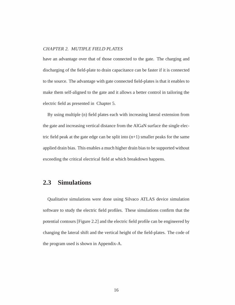
Figure 2.6: The simulated electric field profiles of a device with two field-platesshows that with increasing the lateral spacing leads to the peaks spatially seper-ated.
because thereafter the electric field peaks get spatially seperated. The interme-
diate regions between the peaks do not significantly contribute to the potential
supported, but they contribute to the additional gate capacitance [Figure 2.6].
21

CHAPTER 2. MUTIPLE FIELD PLATES
29nm AlGaN2Deg
substrate
0.5um GaN:Fenucleation
1.8um GaN:UID
Source SourceGate
Drain
Figure 2.7: The epitaxial structure of the HEMT and the layout of the fabricateddevices.
2.4 Device Fabrication and results
The AlGaN/GaN HEMT epitaxial structure was grown by Metal Organic
Chemical Vapour Deposition(MOCVD) on a c-plane Sapphire substrate. The
epitaxial growth was initiated with a 50 nm AlN nucleation layer followed by
a 0.7µm Fe-doped GaN layer. This was followed by a 1.8µm thick uninten-
tionally doped(UID) GaN layer and a 29 nm thick AlGaN heterostructure. The
sample was capped with an insitu grown 4nm thick SiNx as gate dielectric to
reduce gate leakage. Hall measurements at room temperature showed a channel
carrier concentration of 8.59×1012 cm−2 and mobility of 1310 cm2/V·s.
22

CHAPTER 2. MUTIPLE FIELD PLATES
0 5 10 15 20 25 30 350
100m
200m
300m
400m
500m
600m
700m
Ids
(A/m
m)
Vds (V)
dc80us
0 5 10 15 20 25 30 350
100m
200m
300m
400m
500m
600m
700m
800m
Ids
(A/m
m)
Vds (V)
dc80us
Figure 2.8: (a) Before passivation there is significant dispersion between dc andpulsed-80µsIV curves (b) After passivation the dispersion is eliminated.
The AlGaN/GaN HEMTs made in this run used a T-shape layout [Figure 2.7]
with a gate of width 2×25µm. The gate length used was 1.5µm and 2µm and the
gate-drain distance varied from 4µm to 28µm. First, Ti/Al/Ni/Au(20/120/30/50nm)
ohmic metals were deposited and annealed at 870◦C in a RTA chamber to get
ohmic source and drain contacts. The devices were then mesa-isolated by etch-
ing in a Cl2 reactive ion etcher. Ni-Au-Ni(30/400/30nm) gates were deposited
by a lift-off process. Devices were then tested using tek370A curve tracer. They
were found to have RF dispersion and the three terminal breakdown voltage in-
creased with increasing gate-drain spacing. For Lgd=24µm the breakdown volt-
age was between 300-400 V. This breakdown voltage decreased to about 250V
23

CHAPTER 2. MUTIPLE FIELD PLATES
GateGate
FP1 FP1 FP2 FP2
FP3 FP3
Figure 2.9: SEM picture of the cross-section of the fabricated device with threefield-plates.
after a surface passivation done by depositing about 120 nm SiN by Plasma En-
hanced Chemical Vapour Deposition (PECVD). The current-voltage(I-V) char-
acteristics measured at DC and 80µs are shown in Figure 2.8. The devices
showed high current density (700 mA/mm) with no dispersion at the measured
frequency.
By shifting the gate layer mask towards the drain the lithography for the first
field-plate was patterned. The field-plate (Ni/Au 30/400 nm) is connected to the
gate at the gate pad region. The field-plate extension was s1=0.5-0.7µm. On top
24

CHAPTER 2. MUTIPLE FIELD PLATES
Figure 2.10: With two field-plates a breakdown voltage of 900V was achievedon a device with Lg=2µm and Lgd=24µm
of this another 120nm thick SiN was deposited by PECVD. An increase in the
breakdown voltage was observed. Devices with Lgd=24µm had a three terminal
breakdown voltage of 600-700 V. This process was repeated to get the second
field-plate shifted further towards the drain [Figure 2.9]. The extension of the
second field plate was s2=0.5-0.7µm and the device was capped with another
120 nm thick layer of SiNx deposited by PECVD. After this step the breakdown
voltage increased further. Devices with Lgd=24µm showed a three terminal
breakdown voltage of 900 V as shown in Figure 2.10. The measured three ter-
25
CHAPTER 2. MUTIPLE FIELD PLATES
after gate passvtn 1st FP 2nd FP0
100200300400500600700800900
1000
Bre
akdo
wn
Volta
ge (V
)
Measurements
Lg = 1.5 umLgd = 24 um
3rd FPafter gate passvtn 1st FP 2nd FP0
100200300400500600700800900
1000
Bre
akdo
wn
Volta
ge (V
)
Measurements
Lg = 1.5 Lgd = 24
3rd FP
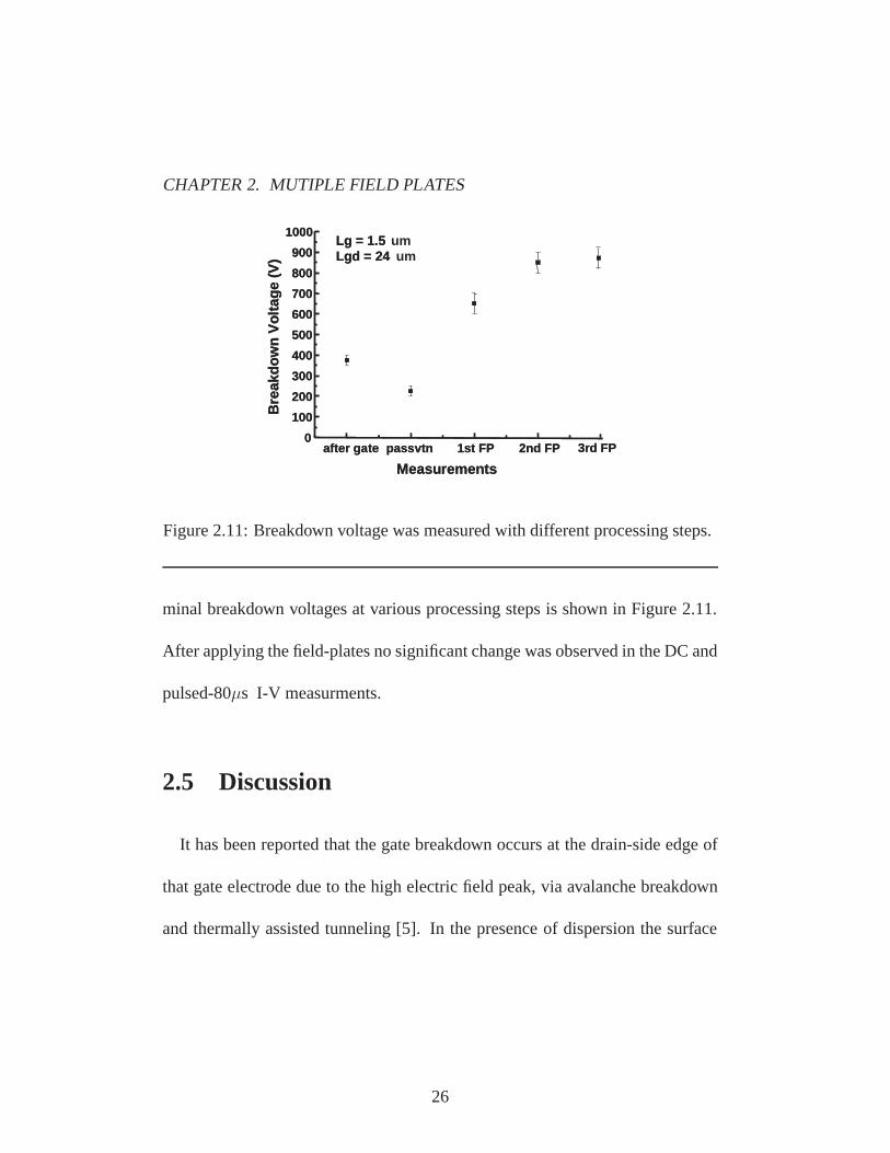
Figure 2.11: Breakdown voltage was measured with different processing steps.
minal breakdown voltages at various processing steps is shown in Figure 2.11.
After applying the field-plates no significant change was observed in the DC and
pulsed-80µs I-V measurments.
2.5 Discussion
It has been reported that the gate breakdown occurs at the drain-side edge of
that gate electrode due to the high electric field peak, via avalanche breakdown
and thermally assisted tunneling [5]. In the presence of dispersion the surface
26

CHAPTER 2. MUTIPLE FIELD PLATES
traps are negatively charged at pinch-off. This extends the effective gate length
and reduces the peak electric field at the drain side edge of the gate. Due to this
mitigation of the electric field before passivation, devices show higher break-
down voltage (>350 V). But they also show dispersion due to the slow response
of the surface traps. When dispersion is removed by surface passivation the peak
electric field at the drain side edge of the gate increases drastically. This ex-
tremely large electric field peak can cause local Schottky-barrier breakdown at
lower drain bias. Thus electric field engineering in the proximity of the gate is
necessary to improve the device performance.
The multiple field-plates technique is effective in alleviating the electrical field
crowding at the drain-side edge of the gate. As simulations and experiments
have demonstrated the multiple field-plates technique is effective in extending
the drain depletion region and replacing the single peak electric field with n+1
peaks with smaller electric field strength (n is the number of field-plates). Since
the field-plates increase the effective gate capacitance it leads to slight degrada-
tion of the high frequency performance. For devices with Lg=0.7µm, the ft is
typically about 20 GHz. From this, for Lg=2µm an ft= 7 GHz is expected, but
the measured ft is only about 4.5 GHz due to the additional capacitance from
27

CHAPTER 2. MUTIPLE FIELD PLATES
100M 1G 10G
1
10
ft=4.5 GHz
fmax
=12 GHz
Mag
nit
ud
e
Frequency (Hz)
|h21||U|
Figure 2.12: Small signal measurements of a device with Lgd=20µm, Lg=2µm,s1=0.5µm, s2=0.5µm, s3=1µm at a bias of Vds=15 V, Ids=280 mA/mm
the field-plates [Figure 2.12]. However this technique is especially attractive for
power electronics application below 1 GHz range.
This technique of using multiple field-plates over the passivation dielectric
uses simple and well controlled processing steps. The active device area is pro-
tected from possible damages in the subsequent processing steps by the passiva-
tion dielectric, thereby not affecting the processing yield.
28
CHAPTER 2. MUTIPLE FIELD PLATES
2.6 Summary
The need for using multiple field plates to achieve both high breakdown volt-
age and high frequency operation was presented. Simulations showed the ex-
pected trends in the electric field profiles in the presence of field-plates. A
strategy for optimizing the parameter space for the field-plates was presented.
Fabricated devices with field-plates showed a higher breakdown voltage than the
devices without field-plates. With two field-plates a breakdown voltage of 900 V
was obtained. The field-plates lead to a slight degradation in the frequency re-
sponse due to the additional capacitance contributed by the field-plates.
References
[1] U. K. Mishra, P. Parikh, Y. Wu,“AlGaN/GaN HEMTs - An Overview of De-vice Operation and Applications”.Proceedings IEEE, 90, pp 1022 (2002).
[2] R. Vetury, N. Q. Zhang, S. Keller, and U. K. Mishra,“The impact of surfacestates on the DC and RF characteristics of AlGaN/GaN HFETs”. IEEE Elec-tron Device Letters, vol 48, pp 560-566, March 2001.
[3] Robert Coffie ,“Characterizing and Suppressing DC-to-RF Dispersion in Al-GaN/GaN High Electron Mobility Transistors”. PhD thesis, University ofCalifornia, Santa Barbara, 2003.
[4] S. Karmalkar, U. K. Mishra,“Enhancement of breakdown voltage in Al-GaN/GaN high electron mobility transistors using a field plate”, Electron De-vices, IEEE Transactions on , vol.48, no.8 pp.1515-1521, Aug 2001.
29

CHAPTER 2. MUTIPLE FIELD PLATES
[5] R. J. Trew, U. K. Mishra,“Gate breakdown in MESFETs and HEMTs”.IEEEelectron device letters, 12(10), 524 (1991).
30

3Gate Leakage in AlGaN/GaN HEMTs
3.1 Introduction
GaN has emerged as a promising material for the high speed, high power
device applications. The large bandgap and the high electron velocity
make it suitable for high power microwave applications [1]. However, GaN
metal semiconductor field-effect transistor (MESFET) and AlGaN/GaN high
electron mobility transistor (HEMT) devices suffer from high gate leakage cur-
rent which reduces the reliability and efficiency of the devices. High gate leak-
age current prevents the GaN MESFETs from reaching their potential for high
power levels [2]. Field effect transistors require low gate leakage current for low
noise and improved reliability. Considerable interest in this issue has initiated
the exploration of dielectrics to reduce the gate leakage in the GaN materials
31
CHAPTER 3. GATELEAKAGE
system.
As discussed in §2.2 dc-to-rf dispersion in GaN transistors is normally ad-
dressed by surface passivation employing PECVD deposited SiNx. It is nec-
essary that the gate dielectrics explored for GaN transistors should incorporate
surface passivation to maintain high power performance.
3.2 The origin of gate leakage
Solving the problem of gate leakage needs an understanding of where ex-
actly the leakage happens. Gate leakage is measured after passivation as a two-
terminal measurement between gate and drain with source left floating. Gate
leakage does not depend on the Lgd spacing as shown in Figure 3.1. Gate leak-
age scales faithfully with device width. The linear fit of the data shows that the
leakage is happening throughout the width of the device. The y-intercept seen
could be either the parasitic leakage in the mesa regions and in the region where
the gate feed runs over the mesa wall or it could arise out of measurement scat-
ter from device to device. Gate leakage does not change with gate length (from
0.7µmto 2µm). This shows that the leakage though occuring throughout the
32

CHAPTER 3. GATELEAKAGE
0V 5V 10V 15V 20V 25V1µ
10µ
100µ
1m
10m Ig vs L gd
Gat
eLea
kage
(A
/mm
)
Vdg (V)
Lgd= 2um Lgd= 15um Lgd= 20um
0.0 0.5 1.0 1.5 2.0 2.50.0
0.5
1.0
1.5
2.0
2.5
3.0
R=0.998 linear fit
Ig vs W g scaling
Ig(mA) = 0.26 + 1.1xWg(mm)
Ig (
mA
) at
Vds
=25V
Wg (mm)
Figure 3.1: (a)Gate Leakage does not change with different Lgd spacing (b)Gateleakage scales faithfully with device width Wg.
width of the gate is not occuring throughout the length of the gate. This implies
that the leakage is happening at the drain end of the gate where the E-field is
higher than the other regions of the gate.
A possible source of gate leakage is that the passivating SiNx layer could be
conducting. To study the leakage in the passivating layer, a controlled experi-
ment was performed in which the leakage path in the SiNx was isolated. This
was done by etching trenches in the SiNx by shifting the gate lithography [Fig-
ure 3.2]. The distance of these isolation trenches were varied to study their effect
on leakage. Devices with these isolation trenches in SiNx showed a gate leakage
similar to the device without the isolation trenches. This experiment shows that
33

CHAPTER 3. GATELEAKAGE
SiNx
AlGaN
GaN
DrainSourceGate
AlGaN
GaN
DrainSource
SiN Isolation at 1.1um
Gate
1.1umx
SiNx
AlGaN
GaN
DrainSourceGate
AlGaN
GaN
DrainSource
SiN Isolation at 1.6um
Gate
x1.6um
0 5 10 15 20 251µ
10µ
100µ
1m
10m
Normal device I solation at 1.6um I solation at 1.1um
Gat
eLea
kage
(A
/mm
)
Vdg (V)
Gate L eakage with S iNx isolated
SiNx
AlGaN
GaN
DrainSourceGate
AlGaN
GaN
DrainSource
Standard Device
Gate
Figure 3.2: Controlled experiments to check if the gate leakage is through thepassivating SiN layer. Leakage remains the same after isolating the SiN layer byetching trenches of 0.7µmlength.
the leakage path is not through SiNx.
The above experiments show that the leakage path is through the AlGaN layer
at the drain end of the gate. To study whether the leakage in the AlGaN is
occuring at the dislocation sites, a HEMT was grown on a double-LEO GaN
substrate which had lower dislocation density (1×107cm−2). The HEMT made
on this sample had a similar gate leakage of 1 mA/mm as seen in a standard
HEMT made on other substrates (with dislocation density of 1×109cm−2). If the
34

CHAPTER 3. GATELEAKAGE
0 5 10 15 20 2510n
100n
1µ
10µ
100µ
1m
10m
after passivationbefore passivation
Gat
eLea
kage
(A
/mm
)
Vdg (V)0 2 4 6 8 10 12 14 16
0
200
400
600
800
1kMax.Vg = 1VDel.Vg= -1V
Dra
in C
urre
nt (
mA
/mm
)
Drain V oltage (V)
200ns80usdc
Figure 3.3: After passivation the gate leakage in HEMTs grown on LEO GaNtemplate is about 1 mA/mm (comparable to those devices on ordinary tem-plates).
dislocation density is known, one could estimate the current that the dislocations
have to support. Assuming a dislocation density of 1×107cm−2, a high E-field
region of 0.1µm length and a width of 1 mm, the number of dislocations present
in this area can be estimated as 10. This means that if dislocations were the
only paths of gate leakage, then these 10 dislocations must pass 1mA of current
which turns out to be a very high current density. So it could be argued that
the gate leakage could occur in AlGaN even without the aid of dislocations,
due to the high electric field peak at the drain side of the gate edge. This is
controversial because Yu et al.[3] have shown that the dislocations are the source
35

CHAPTER 3. GATELEAKAGE
of gate leakage on an unpassivated AlGaN/GaN sample grown by MOCVD. The
exact mechanism of gate leakage in the AlGaN is not clearly understood.
3.3 Reducing gate leakage
3.3.1 Reducing gate leakage by using trench gates
One processing variation that reduced the gate leakage in the HEMTs even
without the use of any dielectric is the trench gate process. In this process tech-
nology the passivation is done before the gates and trenches as defined by the
gate lithography are etched in the passivation using Reactive Ion Etching(RIE
conditions: 20 mT chamber pressure, 20/2 sccm CF4/O2 gas flow). Gates are de-
posited in these trenches using the same lithography in a self-aligned way. Also
during the metal evaporation the angle at which the sample receives the metal
flux could be changed to get a self-aligned field-plate intimately connected to
the gate. Also the shape of the profile of the SiNx trench walls could be changed
by changing the etch conditions. For example a high chamber pressure (20 mT)
during the etch yields a considerable flux of reactive ions in the RIE sideways
36

CHAPTER 3. GATELEAKAGE
0 5 10 15 20 251µ
10µ
100µ
1m
10m
Gat
eLea
kage
(A
/mm
)
Vdg (V)
std gates trench gates
SiNx
AlGaN
GaN
DrainSourceGate
AlGaN
GaN
DrainSource
Standard Gate
Gate
AlGaN
GaN
SourceGate
GaN
Trench gate
SiNxGate
DrainSourceAlGaN
Figure 3.4: Gate leakage is reduced by a factor of 5 by using the trench-gateprocess, in which the passivation is done first and the gate is deposited in thetrench etched in the passivation layer.
and this yields a sloping trench wall. Also by changing the CF4/O2 gas ratio the
rate of etch of the Photoresist relative to the etch rate of the passivation layer
could be changed thereby allowing another parameter to control the trench wall
profile. By varying the angle of E-beam gate metal evaporation the extension of
the self-aligned field-plate could also be controlled.
Gate leakage was reduced by atleast a factor of 5 by using trench gates. Fig-
ure 3.4 shows the comparison of the gate leakage of devices with normal gates
and devices with trench gates. This reduction in gate leakage could be due to
37

CHAPTER 3. GATELEAKAGE
the formation of a self-aligned field-plate on the sloping trench wall by using an
angled gate metal evaporation. This field-plate reduces the peak E-field yielding
a reduced gate leakage. An additional advantage with the trench gate process is
that it yielded an improved passivation. The trench gate process in presented in
detail in §5.2.
3.3.2 Literature survey of reducing gate leakage in GaN de-
vices using dielectrics
Various dielectric materials have been tried as an insulator underneath the
gate to reduce gate leakage in HEMTs. Chini et al. have used a thin film of SiNx
grown in situ by MOCVD to reduce gate leakage in GaN MESFETs [2]. 4 nm of
SiNx was deposited on the sample surface by flowing disilane and ammonia in-
side the MOCVD chamber at a temperature of 980◦C. Chini et al. attributed the
reduction in gate leakage with the SiNx film to reduced conduction through the
dislocations or due to increased Schottky barrier height. In §3.3.3 the results of
various dielectrics grown by MOCVD is presented. SiO2 deposited by plasma-
enhanced chemical vapor deposition (PECVD) under the gate has been shown
38
CHAPTER 3. GATELEAKAGE
to reduce gate leakage by six orders of magnitude in an AlGaN/GaN HEMT
structure [4]. However the low dielectric constant of SiO2 (εr = 3.9) leads to
a larger pinch-off voltage and reduced gate control in the HEMT. A combina-
tion of sputtered SiNx and Ebeam-evaporated SiOx films have been tried as gate
dielectric to reduce gate leakage [5]. However the devices with that dielectric
showed considerable high frequency dispersion.
In two separate studies Hansen et al. have reported the use of (Ba,Sr)TiO3
(BST) [6] and LiNbO3 [7] thin films deposited by rf-magnetron sputtering as
possible dielectrics for GaN and AlGaN/GaN devices. Hansen et al. performed
a blanket deposition of the films just before the gate metallization step. However
they observed that the surface was damaged by the high ion energies associ-
ated with the sputtering process which resulted in reduced electron density and
reduced electron mobility in the two-dimensional electron gas (2DEG) at the
AlGaN/GaN interface. Oxides such as crystalline gadolinium oxide (Gd2O3)
and amorphous gadolinium gallium oxide Ga2O3(Gd2O3) have been tried in
GaN devices using molecular beam epitaxy to achieve low interface state den-
sity between the dielectric and the substrate [8]. MgO and Sc2O3 deposited by
RF plasma-assisted molecular beam epitaxy have been tried as high-k gate di-
39
CHAPTER 3. GATELEAKAGE
electrics for AlGaN/GaN devices [9]. The pulsed-IV curves reported in these
studies show reduced DC-to-RF dispersion [10].
Thin metallic Zr and Hf films have been oxidized by ozone to yield high-k gate
oxide dielectrics for Si and Si-Ge material system [11]. The ozone is generated
by exposure of oxygen gas to ultraviolet (UV) radiation from a Hg vapor lamp.
A high dielectric constant, large bandgap (Eg 5.8 eV), large conduction band
offset with Si ( Ec 1.4 eV) and reduced charge trapping make these oxides very
promising dielectrics for Si [12]. ZrO2 is also reported to have breakdown fields
above 3 MV/cm [13] making it a potential candidate as a dielectric for large
bandgap, high power material system like GaN. The low energy deposition of
Zr followed by the UV-ozone oxidation at relatively lower temperatures could
enable this film to be easily incorporated into the GaN process flow. In §3.3.4
the use of ZrO2 as a high-k dielectric for the GaN material system is presented.
3.3.3 Reducing gate leakage by using in-situ grown dielectrics
Various dielectric materials grown by MOCVD were tried as candidates for a
gate dielectric for GaN transistors. These dielectrics were grown at high temper-
40

CHAPTER 3. GATELEAKAGE
60V80V50V50V70V60V 100V2T-GDBreakdown
67uA/mm
160V
0.03uA/mm
4nmAlOx
830uA/mm
130V
14uA/mm
BuriedSiNx
100uA/mm
210V
0.7uA/mm
6nmSiNx
1000uA/mm
130V
200uA/mm
4nmSiNx
500uA/mm
150V
30uA/mm
2nmSiNx
330 uA/mm
120V
3uA/mm
0.5nmSiNx
Afterpassivation
150V2T-GDBreakdown
Std.HEMT
Beforepassivation
670uA/mm
Gate LeakageVds = 18V;Vgs = -6V;
0.133 uA/mm
Gate LeakageVds = 18V;Vgs = -6V;
60V80V50V50V70V60V 100V2T-GDBreakdown
67uA/mm
160V
0.03uA/mm
830uA/mm
130V
14uA/mm
100uA/mm
210V
0.7uA/mm
1000uA/mm
130V
200uA/mm
500uA/mm
150V
30uA/mm
330 uA/mm
120V
3uA/mm
Afterpassivation
150V2T-GDBreakdown
Beforepassivation
670uA/mm
Gate LeakageVds = 18V;Vgs = -6V;
0.133 uA/mm
Gate LeakageVds = 18V;Vgs = -6V;
031005FA 031005FB 031005FC 031006FB 031006FA 031014FA 031016OH
Figure 3.5: Gate leakage of devices made on HEMT samples with in-situMOCVD grown dielectrics.
ature (> 950◦C) in the MOCVD reactor. They were grown in-situ in MOCVD
reactor after finishing the growth of HEMT epitaxy. The samples had SiNx of
various thicknesses and AlOx on the surface of the HEMT expitaxy. The SiNx
was deposited on the sample surface by flowing di-silane and ammonia inside
the MOCVD chamber at a temperature of 980◦C. One sample had a buried SiNx
layer 4 nm beneath the surface of the HEMT epitaxy which was achieved by
41

CHAPTER 3. GATELEAKAGE
interupting the AlGaN growth, depositing SiNx and growing 4 nm of AlGaN on
top of it. The AlOx was deposited on the sample surface by flowing tri-methyl
aluminum and oxygen inside the MOCVD chamber at a temperature of 900◦C.
The data, summarized in Figure 3.5, was not conclusive. One issue with these
dielectrics was that these films cracked during the 870◦C ohmic anneal step dur-
ing processing. These cracks were seen in the ohmic regions. The uniformity of
these films is also an issue. Devices next to each other sometimes had differing
gate leakage values. This could also be due to the cracking of the film during
the 870◦C anneal. To use such dielectrics improved deposition conditions need
to be employed.
3.3.4 Reducing gate leakage by using ZrO2 dielectric
Zirconium Oxide was tried as a high-k gate dielectric for GaN transistors.
The deposition process for the ZrO2 film was optimized by the analysis of metal
oxide semiconductor capacitor (MOSCAP) structure made on GaN and with
surface characterization techniques. This work was done at UCSB by Sooyeon
Han, Dr. Peter J. Hansen and Dr. Dmitri O. Klenov. Atomic Force Microscopy
42
CHAPTER 3. GATELEAKAGE
SiNx
AlGaN
GaN
DrainSourceGate
AlGaN
GaN
DrainSourceGate
ZrO2
AlGaN
GaN
DrainSourceGate
AlGaN
GaN
DrainSourceGate
ZrO2
AlGaN
GaN
DrainSourceAlGaN
GaN
DrainSource
ZrO2
AlGaN
GaN
DrainSourceAlGaN
GaN
DrainSource
AlGaN
GaN
AlGaN
GaN
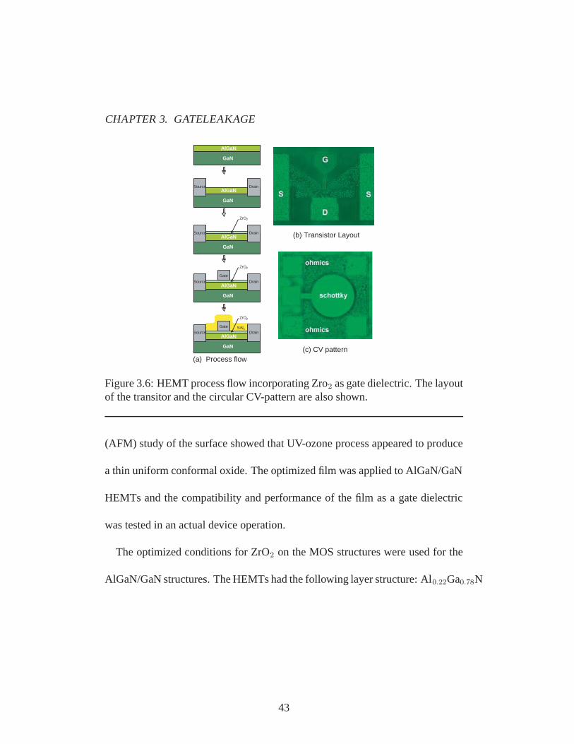
(a) Process flow(c) CV pattern
(b) Transistor Layout
Figure 3.6: HEMT process flow incorporating Zro2 as gate dielectric. The layoutof the transitor and the circular CV-pattern are also shown.
(AFM) study of the surface showed that UV-ozone process appeared to produce
a thin uniform conformal oxide. The optimized film was applied to AlGaN/GaN
HEMTs and the compatibility and performance of the film as a gate dielectric
was tested in an actual device operation.
The optimized conditions for ZrO2 on the MOS structures were used for the
AlGaN/GaN structures. The HEMTs had the following layer structure: Al0.22Ga0.78N
43

CHAPTER 3. GATELEAKAGE
(29 nm)/unintentionally-doped GaN (UID GaN, 1.8 µm)/GaN:Fe (0.5 µm)/AlN
(50 nm)/Sapphire Substrate. Room temperature Hall measurements on the HEMT
samples showed a 2DEG carrier concentration of 8×1012 cm−2 and a mobility
of 1700 cm2/V·s.
The HEMT fabrication started with the liftoff of the Ti/Al/Ni/Au (20/120/30/50 nm)
ohmic contact metallization and annealing at 870◦C in an N2 environment for
30 sec in the RTA. Isolation of the devices was achieved by etching a mesa to
a depth of about 120 nm by Cl2-based reactive ion (RIE) etching. The sample
surface was then cleaned by an O2 plasma de-scum followed by a dip in HCl:DI
= 1:2 for 30 sec to remove any native gallium oxide and a DI rinse. The sam-
ples were pumped overnight in the electron beam evaporator to a pressure of
9×10⁻⁷ torr. A 4 nm Zr film was electron beam deposited. The samples were
quickly transferred to the UV-ozone oxidation chamber with Hg-lamps and a
heated stage. The Hg vapor lamp emits wavelengths of 185 and 254 nm which
are close to the bond energy of O2. This radiation interacts with oxygen gas to
produce oxygen radicals and ozone. This activated oxygen enhances the kinetics
of oxidation compared to natural oxidation, resulting in better oxidation even at
room temperature [14]. The samples were oxidized by the UV-ozone oxidation
44

CHAPTER 3. GATELEAKAGE
Glue
AlGaN
ZrO2
(a)
Glue
ZrO2
AlGaN(b)
Figure 3.7: The high resolution Transmission electron Microscope imagesa)HRTEM and b)HAADF-STEM. This characterizatin was done by Dr. DmitriO. Klenov at UCSB.
method for 30 min at 300◦C. Ni/Au/Ni gates were defined by lift-off. In the
AlGaN/GaN HEMT samples, after the gate metallization the surface was passi-
vated with PECVD grown SiNx of thickness 120 nm to remove dispersion. A
schematic of the HEMT process flow is shown in Figure 3.6a.
The test structures on the HEMT samples consisted of the HEMT devices
(Figure 3.6b) and circular CV pattern with a guard ring (Figure 3.6c). The gate
width and gate length of the transistors measured were 150 µm and 0.7 µm,
respectively. The source-to-drain spacing was 3.4 µm. Electrical characteriza-
45

CHAPTER 3. GATELEAKAGE
tion included CV, gate leakage, pulsed-IV and load-pull power measurements.
Capacitance-voltage measurements were performed with a Keithley-590 CV me-
ter at 1 MHz. The leakage current measurements were made using a HP 4145
semiconductor parameter analyzer. The load-pull power measurements on the
HEMTs were performed on a Maury 2-18 GHz load-pull system.
Cross-sectional TEM micrographs done by Dmitri O. Klenov showed that
4 nm of evaporated Zr resulted in an uniform thickness of the ZrO2 film of ap-
proximately 5 nm. Both High Resolution Transmission Electron Microscope
(HRTEM) and High-Angle Annular Dark Field Scanning Transmission Electron
Microscopy (HAADF-STEM) images showed that the ZrO2 was amorphous. In
addition, no crystallization was observed by nanodiffraction. However, some
degree of nanocrystallinity could not be excluded [15]. HRTEM images (Fig-
ure 3.7a) showed an abrupt interface between AlGaN and ZrO2 and no reaction
layer was found. The HAADF-STEM images (Figure 3.7b) showed the absence
of any reaction layer between AlGaN and ZrO2 though a greater roughness of
the AlGaN surface was observed than expected, which may be due to some de-
gree of oxidation of the AlGaN during ozone oxidation. Direct evidence of the
oxidation of AlGaN is not available.
46
CHAPTER 3. GATELEAKAGE
SiNx
AlGaN
GaN
DrainSourceGate
AlGaN
GaN
DrainSource
Standard Gate
Gate SiNx
AlGaN
GaN
DrainSourceGate
AlGaN
GaN
DrainSource
Gate with ZrO
Gate
2ZrO2
0V 5V 10V 15V 20V10p
100p1n
10n100n
1µ10µ
100µ1m
10m
standard gates gates with Z rO2
(300°C)
Gat
e L
eaka
ge (
A/m
m)
Vdg (V)-6 -4 -2 0 2
0F
20pF
40pF
60pF
80pF
100pF
Cap
acita
nce
(F)
Voltage (V)
standard gates gates on Z rO2
Figure 3.8: Gate leakage is reduced by 2 orders using zirconium oxide dielec-tric(oxidized at 300◦C).
In AlGaN/GaN HEMTs, PECVD deposition of SiNx (performed at 250◦C)
passivates the surface of the AlGaN. Therefore to achieve a high quality of pas-
sivation, it is necessary that the temperature and the time for which the AlGaN
surface is subjected to oxidation should be limited to as close to 250◦C as pos-
sible. So an optimum temperature of 300◦C and a time of 30 min for the UV
oxidation step were chosen for all the AlGaN/GaN HEMT samples so that the
passivation would not be seriously affected.
47
CHAPTER 3. GATELEAKAGE
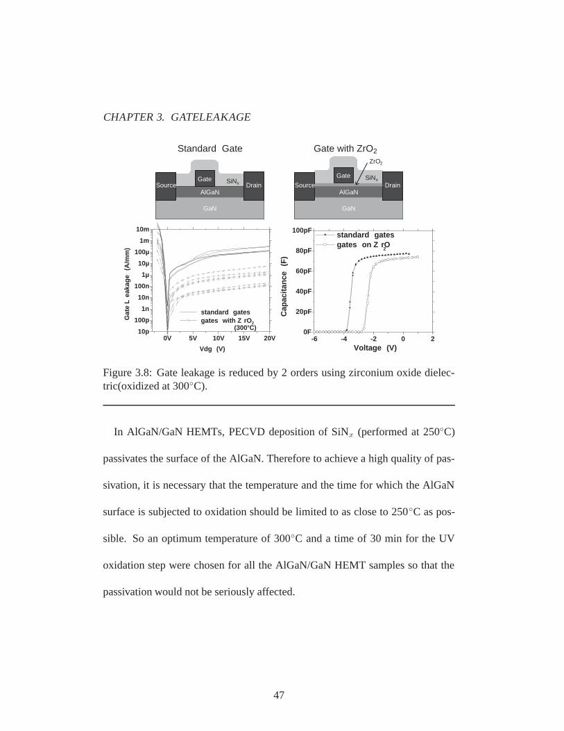
The gate leakage in the AlGaN/GaN HEMTs was reduced by at least two or-
ders of magnitude with ZrO2 as a gate dielectric [Figure 3.8] in comparison to
the Schottky gates. All gate leakage measurements were performed after the
devices were passivated with SiNx. After passivation, the DC-to-RF dispersion
was reduced, but the peak electric field increased because all the electric field
lines terminate at the drain edge of the gate. Thus, measurements of gate leak-
age after passivation ensured that the high electric field at the drain side of the
gate was the same as in the high frequency high power operation of HEMTs.
Figure 3.8 compares the CV measurements with and without ZrO2 under the
gate. By comparing the capacitance values at a gate bias for which there is still
an undepleted 2DEG, the relative dielectric constant for the ZrO2 layer was ex-
tracted to be εr=23 . This value of dielectric constant agreed with the numbers
reported by others for amorphous ZrO2 [16]. The absence of any significant shift
in the CV curve between the positive and negative sweeps demonstrated that the
ZrO2-AlGaN interface had insignificant charge trapping. The global shift in the
CV curve by about 1V towards the right, exhibiting a reduced pinch-off voltage,
is attributed to the reduction in the 2DEG concentration (delta ns = 2.5×10¹²
cm−2) at zero gate bias after the oxidation process, suggesting a change in sur-
48
CHAPTER 3. GATELEAKAGE
SiNx
AlGaN
GaN
DrainSourceGate
AlGaN
GaN
DrainSource
Surface oxidized with Zr film
Gate
ZrO2
SiNx
AlGaN
GaN
DrainSourceGate
AlGaN
GaN
DrainSource
Surface oxidized without Zr film
Gate
Surface oxide
-5V 0V 5V 10V 15V 20V 25V10p
100p1n
10n100n
1µ10µ
100µ1m
10m
without oxidation oxidized without zr oxidized with zr
Gat
eLea
kage
(A
/mm
)
Vdg (V)
Figure 3.9: Controlled experiment performed by UV-Ozone oxidation of deviceswith zirconium film deposited on AlGaN and devices without zirconium film onAlGaN show that the reduced gate leakage is due to the zirconium oxide and notdue to the surface oxidation of AlGaN.
face fermi-level position at the AlGaN/ZrO2 interface. However the reduction in
the zero bias 2DEG concentration did not affect the device performance, because
with ZrO2 the device could be biased to more positive voltages, thus inducing
additional 2DEG concentration.
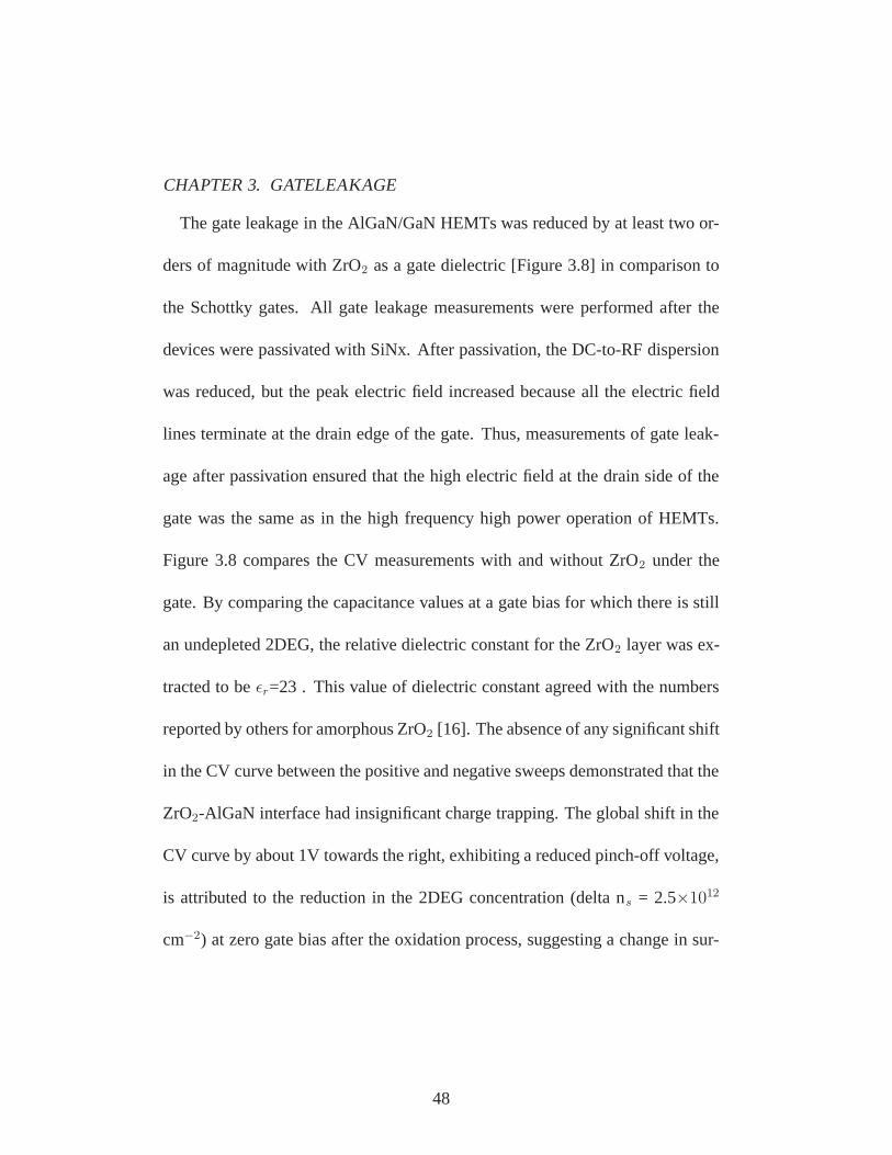
To verify whether the gate leakage reduction was due to ZrO2 or due to surface
oxidation of AlGaN, a controlled experiment was performed. One of the sam-
ples was partially shadow masked during the electron beam evaporation of Zr.
Thus part of the sample had Zr deposited on it and the rest had the bare AlGaN
49

CHAPTER 3. GATELEAKAGE
0 2 4 6 8 10 120
200
400
600
800 max V g = 1 Vdel V g = -1 V
Dra
in C
urre
nt (
mA
/mm
)
Drain V oltage (V)
200 ns 80 us dc
0V 5V 10V 15V 20V 25V10p
100p
1n
10n
100n
1µ
10µ
100µ
1m
fresh deviceafter pulsed-IVafter 15V V ds power
Gat
eLea
kage
(A
/mm
)Vdg (V)
Figure 3.10: Using ZrO2 leads to dispersion as shown in these pulsed-IV curves.The gate leakage reduction gradually degrades with pulsed-IV measurementsand finally with 4GHz load-pull power measurements.
surface. The entire sample was oxidized by the UV-ozone oxidation method at
300◦C for 30 min. Gates were deposited in both the regions and SiNx passivation
was performed to reduce dispersion. Figure 3.9 shows the comparison of gate
leakage for the AlGaN surface, oxidized with and without Zr. This controlled
experiment clearly showed that the leakage reduction was due to ZrO2 and not
due to surface oxidation of AlGaN.
Two challenges for using ZrO2 as gate dielectric for AlGaN/GaN HEMTs
were observed. One was the effectiveness of the SiNx passivation in the Al-
GaN/GaN HEMTs in the presence of a gate dielectric. Figure 3.10a shows the
50

CHAPTER 3. GATELEAKAGE
high frequency pulsed-IV curves showing knee-walkout compared to the DC IV
curves, commonly referred to as dispersion. Due to the poor thermal conduc-
tivity of the sapphire substrate, a well-passivated AlGaN/GaN HEMT grown on
sapphire substrate is expected to have a peak pulsed-current at least 10% above
that of the peak DC-current. The pulsed-IV curves show lower current level than
the DC current level indicating the presence of dispersion. Another issue is the
stability of the gate dielectric in device operation. Figure 3.10b shows that the
gate leakage degraded after pulsed-IV measurements and 4 GHz load-pull power
measurements at a bias of Vds = 15 V.
To address the issues of dispersion and the dielectric stability, the fabrica-
tion process of the AlGaN/GaN HEMT was changed as shown in Figure 3.11a.
Instead of passivating the HEMT after the gate metal deposition, SiNx was de-
posited first. Using the gate lithography, trenches were etched in the SiNx and
the photoresist was removed. After solvent cleaning, Zr was blanket deposited
and oxidized as described earlier. Finally with another gate lithography aligned
towards the drain side wall of the trench, the gate metal was deposited, simulta-
neously introducing a field-plate effect [17][18].
The pulsed-IV curves shown in Figure 3.11b demonstrate improved passiva-
51
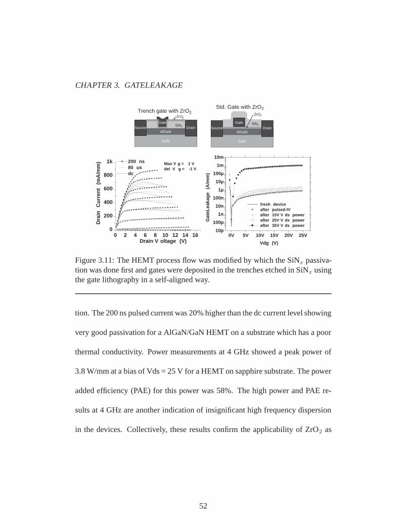
CHAPTER 3. GATELEAKAGE
AlGaN
GaN
SourceGate
GaN
Trench gate with ZrO2
SiNx
ZrOGate
DrainSource
2
AlGaN
0 2 4 6 8 10 12 14 160
200
400
600
800
1k Max V g = 1 Vdel V g = -1 V
Dra
in C
urre
nt (
mA
/mm
)
Drain V oltage (V)
200 ns80 usdc
0V 5V 10V 15V 20V 25V10p
100p1n
10n100n
1µ10µ
100µ1m
10m
fresh device after pulsed-IV after 15V V ds power after 25V V ds power after 35V V ds power
Gat
eLea
kage
(A
/mm
)
Vdg (V)
SiNx
AlGaN
GaN
DrainSourceGate
AlGaN
GaN
DrainSource
Std. Gate with ZrO
Gate
2ZrO2
Figure 3.11: The HEMT process flow was modified by which the SiNx passiva-tion was done first and gates were deposited in the trenches etched in SiNx usingthe gate lithography in a self-aligned way.
tion. The 200 ns pulsed current was 20% higher than the dc current level showing
very good passivation for a AlGaN/GaN HEMT on a substrate which has a poor
thermal conductivity. Power measurements at 4 GHz showed a peak power of
3.8 W/mm at a bias of Vds = 25 V for a HEMT on sapphire substrate. The power
added efficiency (PAE) for this power was 58%. The high power and PAE re-
sults at 4 GHz are another indication of insignificant high frequency dispersion
in the devices. Collectively, these results confirm the applicability of ZrO2 as
52

CHAPTER 3. GATELEAKAGE
gate dielectric for high frequency operation.
Figure 3.11c shows that the gate leakage reduction did not degrade until the
power measurements at Vds bias of 35 V. We believe that the improvement in the
gate leakage degradation is caused by a reduced field peaking, due to the field-
plate effect caused by the alignment of the gate edge over the wall of the SiNx
trench. After the device showed degradation in the gate leakage, the pulsed-IV
and load-pull measurements were performed. After the degradation, however the
current levels and the power levels in the devices did not change. However, the
gate leakage was significantly higher after the degradation, but was on the same
order as a device without any dielectric under the gate. This leads us to believe
that the dielectric degraded under very high field operation. Further investigation
is necessary to improve the high-field reliability of this dielectric.
3.4 Leakage from field-plates:
The leakage through the field-plates was quantified by a device structure with-
out a gate, but with a field-plate sitting on top the passivation dielectric as shown
in Figure 3.12. Such a structure allows for the measurement of the leakage
53
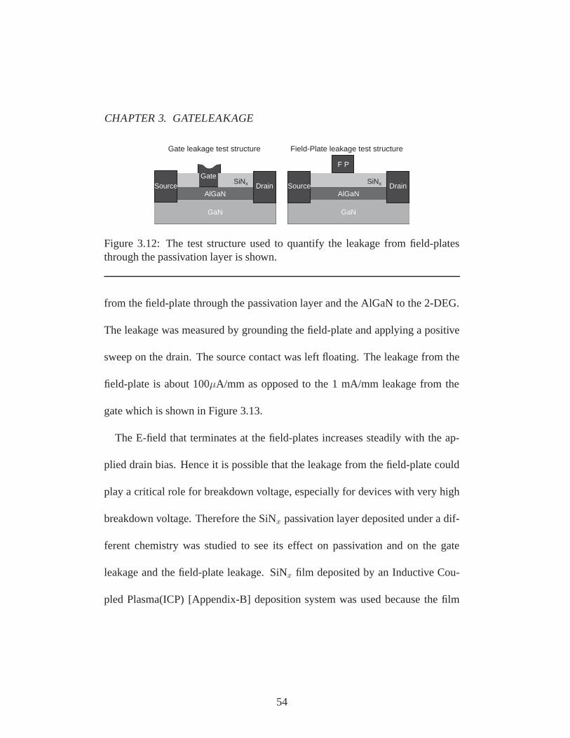
CHAPTER 3. GATELEAKAGE
SiNx
AlGaN
GaN
DrainSourceAlGaN
GaN
DrainSource
Field-Plate leakage test structure
F P
AlGaN
GaN
SourceGate
GaN
Gate leakage test structure
SiNxGate
DrainSourceAlGaN
Figure 3.12: The test structure used to quantify the leakage from field-platesthrough the passivation layer is shown.
from the field-plate through the passivation layer and the AlGaN to the 2-DEG.
The leakage was measured by grounding the field-plate and applying a positive
sweep on the drain. The source contact was left floating. The leakage from the
field-plate is about 100µA/mm as opposed to the 1 mA/mm leakage from the
gate which is shown in Figure 3.13.
The E-field that terminates at the field-plates increases steadily with the ap-
plied drain bias. Hence it is possible that the leakage from the field-plate could
play a critical role for breakdown voltage, especially for devices with very high
breakdown voltage. Therefore the SiNx passivation layer deposited under a dif-
ferent chemistry was studied to see its effect on passivation and on the gate
leakage and the field-plate leakage. SiNx film deposited by an Inductive Cou-
pled Plasma(ICP) [Appendix-B] deposition system was used because the film
54

CHAPTER 3. GATELEAKAGE
0 5 10 15 20 2510n
100n
1µ
10µ
100µ
1m
10m
2-layerSiNx trench gate 2-layerSiNx field plate
S td.SiNx trench gate S td.SiNx field plate
Gat
eLea
kage
(A
/mm
)
Vdg (V)
0 5 10 15 20 25 300
200
400
600
800
1kpulsed IV curves
MaxVg = 1Vdel Vg= -1V
Dra
in C
urr
ent
(mA
/mm
)
Drain Voltage (V)
200ns 50ohmLL 200ns 165ohmLL dc
Figure 3.13: Leakage from field-plates through different passivation layers isshown. The bottom set of curves show the gate leakage and field-plate leakageof the two-layer passivation and the top set of curves show the gate leakageand field-plate leakage of the standard passivation. The pulsed-IV curves of thedevice passivated with two-layer dielectric show little dispersion upto 165ohmloadline.
deposited using this high density plasma is supposed to give a denser film. But
the devices with this passivation had a reduced current of about 1/10th of the
Imax. Exposing the AlGaN surface to this dense plasma seems to have damaged
the surface leading to a reduced current. So a two layer passivation dielectric
was tried in which the first layer of SiNx of 60 nm thickness was depsoited by
PECVD and on top of this a second layer of SiNx of 60 nm thickness was de-
posited by ICP.
55

CHAPTER 3. GATELEAKAGE
Figure 3.13 compares the leakage from the field plates between two passiva-
tion dielectrics. The standard SiNx passivation had gate leakage of 1 mA/mm
and field-plate leakage of 0.1 mA/mm. Devices passivated with the two layer
dielectric had a gate leakage of 0.05 mA/mm and a field-plate leakage of about
0.005 mA/mm. This shows that the field-plate leakage through the two layer
dielectric is insignificant and this dielectric would be useful for devices operat-
ing at high voltages. The pulsed-IV curves of devices passivated with the two
layer dielectric is shown Figure 3.13. For 200 ns pulses there is no dispersion
for a 50 ohm load-line. For a 165 ohm load-line there is little dispersion. These
devices were made using the trench gate process. Further characterization of
this passivation was done by doing power measurements at 4GHz, the details of
which are presented in §5.2.4.
3.5 Summary
The source of gate leakage was studied. The experiments presented show that
the leakage occurs through the AlGaN layer throughout the width of the gate
and at the drain end of the gate. The exact mechanism of leakage in the AlGaN
56

CHAPTER 3. GATELEAKAGE
is not well understood. Various dielectric films were tried as candidates for gate
dielectrics in GaN transistors. In-situ high temperature grown dielectrics have to
deal with the problem of uniformity and compatibility with AlGaN/GaN HEMT
processing. However these high temperature grown dielectrics seem to be reli-
able. Zirconium oxide film made by UV-ozone oxidation of deposited zirconium
film was optimized to serve as a high-k dielectric for GaN transistors. Improved
processing technique enabled the compatibility of ZrO2 as a gate dielectric with-
out compromising passivation. The degradation of this dielectric at high power
operation is an issue. Trench gate processing technique reduced the gate leakage
by a factor of 5. Finally the leakage through the field-plates was studied.
References
[1] U.K. Mishra, P. Parikh, Y. Wu,“AlGaN/GaN HEMTs - An Overview of De-vice Operation and Applications”.
[2] A. Chini, J. Wittich, S. Heikman, S. Keller, S.P. DenBaars, U.K.Mishra,“Power and linearity characteristics of GaN MISFETs on sapphiresubstrate”.IEEE Electron Device Letters, 25, 55 (2004).
[3] E.J. Miller, X.Z. Dang, E.T. Yu,“Gate leakage current mechanisms in Al-GaN/GaN heterostructure field-effect transistors”.Journal of Applied Physics,88, 5951 (2000).
[4] M.A. Khan, X. Hu, A. Tarakji, G. Simin, J. Yang, R. Gaska, M.S.Shur,“AlGaN/GaN metal-oxide-semiconductor heterostructure field-effecttransistors on SiC substrates”.Applied Physics Letters, 77, 1339 (2000).
57

CHAPTER 3. GATELEAKAGE
[5] Naiqian Zhang , “High Voltage GaN HEMTs with Low on-resistance forSwitching Applications”. PhD thesis, University of California, Santa Barbara,2002.
[6] P. J. Hansen, L. Shen, Y. Wu, A. Stonas, Y. Terao, S. Heikman, D. Buttari, T.R. Taylor, S. P. DenBaars, U. K. Mishra, R. A. York, J. S. Speck,“AlGaN/GaNmetal-oxide-semiconductor heterostructure field-effect transistors using bar-ium strontium titanate”.J. Vac. Sci. Technol. B, vol 22(5), pp 2479, Sep 2004.
[7] P. J. Hansen, Y. Terao, Yuan Wu, R. A. York, U. K. Mishra, J. S.Speck,“LiNbO/sub 3/ thin film growth on (0001)-GaN”.J. Vac. Sci. Technol.B, vol 23(1), pp 162-167, Jan 2005.
[8] B.P. Gila, K.N. Lee, W. Johnson, F. Ren, C.R. Abernathy, S.J. Pearton,M. Hong, J. Kwo, J.P. Mannaerts, K.A. Anselm,“A comparison of gal-lium gadolinium oxide and gadolinium oxide for use as dielectrics in GaNMOSFETs”IEEE-Cornell Conference on High performance Devices, 182(2000).
[9] R. Mehandru, B. Luo, J. Kim, F. Ren, B.P. Gila, A.H. Onstine, C.R. Aber-nathy, S.J. Pearton, D. Gotthold, R. Birkhahn, B. Peres, R. Fitch, J. Gille-spie, T. Jenkins, J. Sewell, D. Via, A. Crespo, “AlGaN/GaN metal-oxide-semiconductor high electron mobility transistors using Sc2O3 as the gate ox-ide and surface passivation”. Appl. Phys. Lett. 82, 2530 (2003).
[10] B. Luo, J.W. Johnson, J. Kim, R.M. Mehandru, F. Ren, B.P. Gila, A.H. On-stine, C.R. Abernathy, S.J. Pearton, A.G. Baca, R.D. Briggs, R.J. Shul, C.Monier, J. Han,“Influence of MgO and Sc2O3 passivation on AlGaN/GaNhigh-electron-mobility transistors”. Appl. Phys. Lett. 80, 1661 (2002).
[11] S. Ramanathan, P.C. McIntyre, S. Guha, E. Gusev,“Charge trapping studieson ultrathin ZrO2 and HfO2 high-k dielectrics grown by room temperatureultrviolet ozone oxidation” Appl. Phys. Lett. 84, 389 (2004).
[12] G.D. Wilk, R.M. Wallace, J.M. Anthony,“High-k dielectrics: Current statusand materials properties considerations”. J. Appl. Phys. 89, 5243 (2001).
[13] J. Shappir, A. Anis, I. Pinsky,“Investigation of MOS Capacitors with ThinZrO2 layers and various gate materials for advanced DRAM applications”.IEEE Trans Electron Devices, 33, 442 (1986).
58

CHAPTER 3. GATELEAKAGE
[14] S. Ramanathan, G.D. Wilk, D.A. Muller, C.M. Park, P.C. McIntyre,“Growthand characterization of ultrathin zirconia dielectrics grown by ultravioletozone oxidation”. Appl. Phys. Lett. 79, 2621 (2001).
[15] M.-Y Ho, H. Gong, G.D. Wilk, B.W. Busch, M.L. Green, P.M. Voyles, D.A.Muller, M. Bude, W.H. Lin, A. See, M.E. Loomans, S.K. Lahiri and P.I. Ral-sanen,“Morphology and crystallization kinetics in HfO2 thin films grown byatomic layer deposition” J. Appl. Phys. 93, 1477 (2003)
[16] S. Ramanathan, C. Park, P.C. McIntyre,“Electrical properties of thin film zir-conia grown by ultraviolet ozone oxidation”, J. Appl. Phys., 91, 4521 (2002).
[17] A. Chini, D. Buttari, R. Coffie, L. Shen, S. Heikman, A. Chakraborty, S.Keller, and U. K. Mishra, “Power and linearity characteristics of field-platedrecessed-gate AlGaN-GaN HEMTs”. IEEE Electron Device Letters, vol 25,pp 229-231, May 2004.
[18] Huili Xing, Y. Dora, A. Chini, S. Heikman, S. Keller, U. K. Mishra, “Highbreakdown voltage AlGaN-GaN HEMTs achieved by multiple field plates,”IEEE Electron Device Letters, vol 25, no 4, pp 161-163, April 2004.
59

4Buffer Leakage in GaN Transistors
4.1 Introduction
GaN-based transistors are very promising devices for high power and high
frequency applications. High power levels at microwave-frequencies [1][2]
and high breakdown voltages [3][4] have been demonstrated. To achieve high
performance in lateral devices it is important to have a highly resistive buffer
underneath the conducting channel of the transistor.
AlGaN/GaN High Electron Mobility Transistors (HEMTs) and GaN MEtal
Semiconductor Field Effect Transistors (MESFETs) are made on semi-insulating
GaN buffers grown on substrates like Sapphire, SiC, bulk grown GaN, Si etc,.
Thicker GaN buffers are grown on these substrates to reduce the threading dis-
location density which yields channels with high mobility. In order to achieve
60

CHAPTER 4. BUFFERLEAKAGE
higher breakdown voltage and high power added efficiency it is necessary that
the leakage through the underlying GaN buffer be as low as possible. Resid-
ual donors, presumably oxygen, in the unintentionally doped(UID) GaN, have
been identified as a source of buffer leakage [5][6]. Techniques like incorpo-
rating Fe-doping in Metal-organic chemical vapour deposition(MOCVD) grown
GaN buffers [6] and C-doping in Molecular Beam Epitaxy(MBE) grown GaN
buffers [7] are commonly used to reduce the buffer leakage.
The effect of varying the Fe-doping on the buffer leakage is presented in §
4.3. Alloyed ohmic contacts are identified as another cause of buffer leakage as
described in §4.4. The effect of ohmic contacts on the leakage in the underlying
GaN buffer and its effect on the breakdown voltage of AlGaN/GaN HEMTs is
also presented.
4.2 Test Structures
The epitaxial layer structure used for the GaN devices were grown by MOCVD
on sapphire and 4H-SiC substrates. The epitaxial growth was initiated with a
100 nm thick nucleation layer followed by a 0.5µm thick Fe-doped layer and an
61
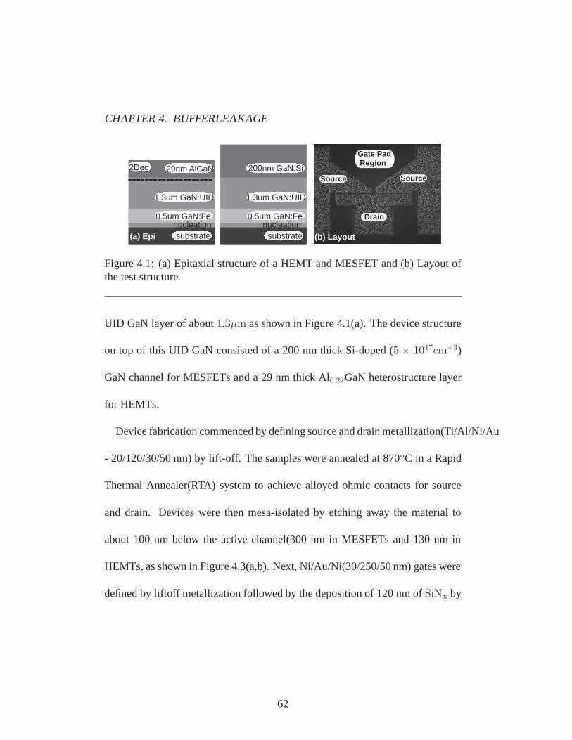
CHAPTER 4. BUFFERLEAKAGE
29nm AlGaN
1.3um GaN:UID
2Deg
0.5um GaN:Fe
substrate nucleation
200nm GaN:Si
1.3um GaN:UID
0.5um GaN:Fe
substrate nucleation
Drain
Source Source
Gate Pad Region
(b) Layout(a) Epi
Figure 4.1: (a) Epitaxial structure of a HEMT and MESFET and (b) Layout ofthe test structure
UID GaN layer of about 1.3µm as shown in Figure 4.1(a). The device structure
on top of this UID GaN consisted of a 200 nm thick Si-doped (5 × 1017cm−3)
GaN channel for MESFETs and a 29 nm thick Al0.22GaN heterostructure layer
for HEMTs.
Device fabrication commenced by defining source and drain metallization(Ti/Al/Ni/Au
- 20/120/30/50 nm) by lift-off. The samples were annealed at 870oC in a Rapid
Thermal Annealer(RTA) system to achieve alloyed ohmic contacts for source
and drain. Devices were then mesa-isolated by etching away the material to
about 100 nm below the active channel(300 nm in MESFETs and 130 nm in
HEMTs, as shown in Figure 4.3(a,b). Next, Ni/Au/Ni(30/250/50 nm) gates were
defined by liftoff metallization followed by the deposition of 120 nm of SiNx by
62

CHAPTER 4. BUFFERLEAKAGE
PECVD at 250oC for passivation. Bondpads were then formed by etching away
the passivating layer on the contact regions. The transistor layout consisted of a
gate with two fingers each of 75µm width as shown in Figure 4.1(b). The gate
length was 0.7µm. The Buffer leakage test pattern used the same layout, but
without the gate and with the channel between the source-drain contacts etched
during the mesa isolation step. Buffer leakage is measured just after the mesa
isolation and before the SiNx passsivation process. Higher leakage values were
observed after passivation but the trends were preserved. The HEMTs had an
Imax ∼1 A/mm, ft ∼20 GHz and fmax ∼50 GHz.
4.3 Effect of Fe-doping level on the buffer leakage
The technique of doping the unintentionally-doped(UID) GaN with Fe yields
semi-insulating buffer for the GaN transistors. The Fe-doping is believed to
introduce traps which affects the high frequency performance of the devices [6].
This drawback is overcome by stopping the Fe-flow after sometime during the
growth and growing UID GaN of about 1µm thickness above the Fe-doped GaN
buffer. The profile of the Fe has been observed not to be abrupt, exhibiting a tail
63
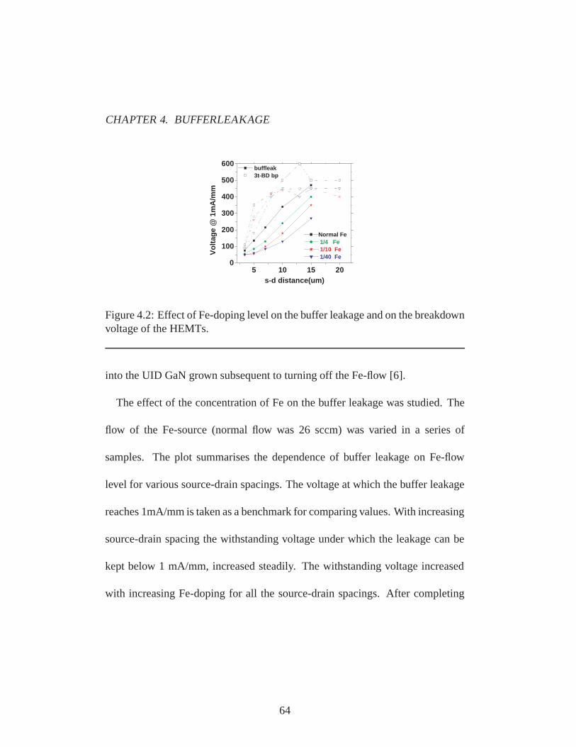
CHAPTER 4. BUFFERLEAKAGE
5 10 15 200
100
200
300
400
500
600
buffleak 3t-BD bp
Vo
ltag
e @
1m
A/m
m
s-d distance(um)
Normal Fe 1/4 Fe 1/10 Fe 1/40 Fe
Figure 4.2: Effect of Fe-doping level on the buffer leakage and on the breakdownvoltage of the HEMTs.
into the UID GaN grown subsequent to turning off the Fe-flow [6].
The effect of the concentration of Fe on the buffer leakage was studied. The
flow of the Fe-source (normal flow was 26 sccm) was varied in a series of
samples. The plot summarises the dependence of buffer leakage on Fe-flow
level for various source-drain spacings. The voltage at which the buffer leakage
reaches 1mA/mm is taken as a benchmark for comparing values. With increasing
source-drain spacing the withstanding voltage under which the leakage can be
kept below 1 mA/mm, increased steadily. The withstanding voltage increased
with increasing Fe-doping for all the source-drain spacings. After completing
64

CHAPTER 4. BUFFERLEAKAGE
the HEMT fabrication the three terminal breakdown voltage of the HEMTs was
measured for the samples with different Fe-doping. The breakdown voltage in-
creased with increasing Fe-doping only for devices with shorter spacing [Fig-
ure 4.2]. For devices with larger spacing the amount of Fe-doping did not show
any consistent difference.
4.4 Effect of ohmic contacts on buffer leakage
4.4.1 Observation of differences in buffer leakage
It was observed that for the same underlying GaN epitaxial growth, the buffer
leakage for the HEMTs was higher than MESFETs [Figure 4.3(a,b,c)]. To in-
vestigate whether this difference comes from the epitaxial growth of the AlGaN
heterostructure or due to the characteristics of device processing, a controlled
experiment was performed, in which a MESFET with a thin channel of 30 nm
was grown, imitating a HEMT with respect to the distance of the surface to the
buffer. This thin-MESFET had a higher buffer leakage [Figure 4.3(b,c,d)] com-
pared to the MESFET with thick channel, thus eliminating the heterostructure
65
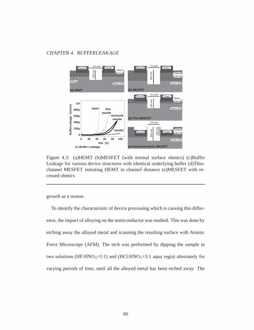
CHAPTER 4. BUFFERLEAKAGE
0 20 40 60 80 1000
200µ
400µ
600µ
800µ
1m
recessed mesfet
thinmesfet
mesfet
hemt
Buf
ferL
eaka
ge (
A/m
m)
Vds (V)
3.4 um
300
nm
160
nm
Source Drain
GaN:UID
200nmGaN:Si
(e) Recessed-ohmic MESFET
Source3.4 um
130
nm
Drain
GaN:UID
30nmGaN:Si
(d) Thin-MESFET
(c) Buffer Leakage
29nmAlGaN
Source
2Deg
3.4 um
130
nm(a) HEMT
Drain
GaN:UID
Source3.4 um
300
nm
Drain
GaN:UID
(b) MESFET
200nmGaN:Si
Figure 4.3: (a)HEMT (b)MESFET (with normal surface ohmics) (c)BufferLeakage for various device structures with identical underlying buffer (d)Thin-channel MESFET imitating HEMT in channel distance (e)MESFET with re-cessed ohmics
growth as a reason.
To identify the characteristic of device processing which is causing this differ-
ence, the impact of alloying on the semiconductor was studied. This was done by
etching away the alloyed metal and scanning the resulting surface with Atomic
Force Microscopy (AFM). The etch was performed by dipping the sample in
two solutions (HF:HNO3=1:1) and (HCl:HNO3=3:1 aqua regia) alternately for
varying periods of time, until all the alloyed metal has been etched away. The
66

CHAPTER 4. BUFFERLEAKAGE
(a) HEMT0 2 4 6 8 10
-100
-50
050
Hei
ght
(nm
)
Scan length (um)
(b) MESFET0 2 4 6 8 10
-100
-50
050
Hei
ght
(nm
)
Scan length (um)
Figure 4.4: Optical microscope picture and AFM scan-section(10µm) of theohmic regions after stripping the alloyed metals a) HEMTs b) MESFETs. Thescan for the HEMTs show upto 100 nm deep pits after the removal of the alloyedmetal. In MESFETs though deep spikes are absent there are smaller peaks andthe alloy reaction proceeds to a depth of about 25∼30 nm into GaN.
optical picture of the resulting surface is presented in Figure 4.4. In the HEMTs
a trace of the ohmic regions could be seen due to the uneven morphology of the
resulting semiconductor surface. In the MESFETs the trace of the ohmic regions
was barely visible.
The resulting surface when scanned with AFM reflected the morphology of
the alloyed reaction into the semiconductor as only the alloyed regions were
67

CHAPTER 4. BUFFERLEAKAGE
29nmAlGaN
Source
2Deg
3.4 um
130
nm
Drain
GaN:UID
(a) HEMT
Source3.4 um
300
nm
Drain
GaN:UID
(b) MESFET
200nmGaN:Si
Source3.4 um
130
nm
Drain
GaN:UID
(c) Thin-MESFET
30nmGaN:Si
160
nm
Source
3.4 um
300
nm
Drain
GaN:UID
(d) Recessed-ohmic MESFET
200nmGaN:Si
Figure 4.5: Morphology of the ohmic contacts explains the difference in bufferleakage in (a)HEMTs (b)MESFETs (with normal surface ohmics) (c)thin MES-FETs imitating the HEMTs (d)MESFETs with recessed ohmics. In HEMTs thedeep spikes are not screened by the 2DEG. In MESFETs deep spikes are ab-sent but there are smaller sharp projections and these are screened well by the Sidoping only in the case of mesfet with surface ohmics.
etched in the acid. In the case of HEMTs 100 nm deep pits were observed
with spiky features [Figure 4.4(a)]. These spiky features could correspond either
to the physical spiking down of the alloyed metal or due to the change in the
crystalline material in those pits which leads to it being etched away by the
alloy-etch solutions. In MESFETs no deep pits were observed in all the cases
studied and the alloyed reaction proceeded in a seemingly uniform manner to a
depth of about 25 ∼ 30 nm into the GaN with shallow pits [Figure 4.4(b)].
68

CHAPTER 4. BUFFERLEAKAGE
4.4.2 Interpretation of Electrical data
To interpret the electrical data, another controlled experiment was performed
in which the distance between the ohmic metals and the bottom edge of the thick
channel of the MESFET was varied. This was done by recessing the ohmic
regions after ohmic lithography in a portion of the wafer. The RIE recess etch
removed about 160 nm of the channel which was originally grown to be 200 nm
thick. The buffer leakage of the devices with normal surface-ohmics and the
devices with recessed-ohmics were compared [Figure 4.3(b)(e)]. The devices
with recessed-ohmics had a higher buffer leakage than the devices with ohmics
deposited on the surface.
The higher buffer leakage current in the HEMTs compared to the MESFETs
can be explained as follows. It is plausible that the electric field lines concentrate
at the spikes due to the lack of screening from the 2DEG [Figure 4.5(a)]. This
field acts on the material that is within and in the vicinity of the spikes which
could be weaker than crystalline GaN. Hence local injection of carriers into the
neighbouring GaN is possible causing the increased buffer leakage. In normal
MESFETs the electric field lines do not concentrate because the sharp points
69

CHAPTER 4. BUFFERLEAKAGE
from the alloying process are screened by the Si-doping [Figure 4.5(b)]. Hence
the reduced buffer leakage in normal MESFETs.
Deep spikes are not necessary to cause this effect. Even if deep spikes are
absent, the region where the alloy-GaN interface lies has an effect on the buffer
leakage. In the case of MESFETs, even though there are no deep spikes like that
of the HEMTs, there are smaller sharp points. Depending on whether the alloy-
GaN interface lies in a doped region or not, it affects the buffer leakage. In the
normal MESFET case, the alloy depth of 30 nm is screened by the underlying
Si doping layer which seems to remove any local E-field peaking. In the case
of the thin-MESFET [Figure 4.5(c)] and in the recessed-ohmic-MESFET [Fig-
ure 4.5(d)], the alloy reaction depth of 30 nm makes the alloy-GaN interface to
reach the undoped region. Since there is no underlying Si-doping to screen any
local E-field peaking at the sharp points, it presumably leads to local avalanche
of carriers.
70

CHAPTER 4. BUFFERLEAKAGE
4.4.3 Interpretation for Morphology
An interpretation is presented to explain why the deep etched spikes are present
only in HEMTs and not in MESFETs. This difference in the alloying behaviour
could be either due to the presence of Si dopants in MESFET channel or due to
the presence of Al in the AlGaN layer of the HEMT.
To study the effect of Si-doping on the morphology of the ohmic contacts, two
MESFETs - one with higher doping density of 2 × 1018cm−3 than the normal
doping of 5 × 1017cm−3 and another with a lighter doping of 1 × 1017cm−3 -
were processed. An intermediate channel thickness of 60 nm was chosen for
these samples to see if this thickness is enough to screen the electric-field. If the
presence of Si were to change the behaviour of the alloying reaction, then the
alloy depth in channels with different dopings would be expected to be different.
This series of samples showed that MESFETs with Si doping of 2 × 1018cm−3
and 1×1017cm−3 did not have deep spikes and had a very similar alloying depth
of about 25∼30 nm. This implies that the presence of Si did not contribute to the
change in morphology of the ohmic alloy. Buffer leakage for both the dopings
in these MESFETs of intermediate thickness was comparable to the MESFET
71

CHAPTER 4. BUFFERLEAKAGE
with 200 nm thick channel. This shows that a channel thickness of 60 nm and a
doping density of 1 × 1017cm−3 are sufficient to screen the E-field peaks.
The presence of deep spikes in the AlGaN/GaN HEMT is reflective of the lo-
calized reactions in the AlGaN layer rather than the uniform reaction observed
in MESFETs. This could be due to a combination of strain in the AlGaN caus-
ing increased reactivity of the dislocations to the alloy-metal stack, and stronger
bond-strength of the AlGaN causing reduced reactivity in the non-dislocated re-
gions. The nature of the TDs participating in these enhanced reaction is unclear
since the densities of pure-edge TDs and TDs with screw components are each
about 5 × 108cm−2 [8] (AlGaN and GaN layers have the same dislocation den-
sities), whereas the ohmic spike density is about 1 × 107cm−2. Since the size
of the ohmic spikes are typically large (100∼500 nm), it is probable that several
dislocations participate in each spiking event explaining the discrepancy in the
densities. Further investigation is needed to clarify the mechanism of the ohmic
spikes in HEMTs.
72

CHAPTER 4. BUFFERLEAKAGE
4.4.4 Ways to reduce the effect of ohmics on buffer leakage in
HEMTs
One way in which the spikes in the ohmic alloy in a HEMT were removed was
to anneal the ohmic metals in the presence of ammonia gas. This eliminated the
spikes under the alloyed ohmic contacts which was confirmed by stripping the
ohmic alloy and scanning the surface using AFM. The buffer leakage on these
devices was much lower than the devices where the ohmic regions were annealed
under normal conditions which result in spiking [Figure 4.6(a)]. The reduced
buffer leakage translates to an increase in the breakdown voltage of the HEMTs
as shown in Figure 4.6(b). To ensure that the enhancement of breakdown was not
a parasitic effect of enhanced dispersion [3][9], pulsed-IV measurements were
performed on these devices. The 200 ns pulsed-IV curves were similar for both
these HEMTs. Also it should be noted that there were no field-plates on these
devices [3].
Though occasionally yielding ohmic contacts to HEMTs without spiky fea-
tures and thus helping to verify our hypothesis, the ammonia anneal process was
not reproducible and neither was a full understanding developed. Techniques
73

CHAPTER 4. BUFFERLEAKAGE
0 20 40 60 80 100 1200
1m
2m
3m
hemtNH3 anneal
hemtstd. anneal
Buf
ferL
eaka
ge (
A/m
m)
Vds (V)0 20 40 60 80 100 120 140 160
0
20m
40m
60m
80m
100m
hemtNH3 anneal
Vgs = -7, -5, -3, -1 (V)
Ids
(A/m
m)
Vds (V)
Figure 4.6: (a)Buffer Leakage reduced in HEMTs by the removal of spikesin ohmic contacts by using NH3 during the anneal (b)Breakdown voltage ofHEMTs increased from 100 V to about 145 V by the removal of alloy-spikes.
such as non-alloyed contacts to n+ cap-layers and implanted regions show more
promise and need to be explored. The removal of the effect of alloyed ohmic
contacts would lower the buffer leakage in the lateral devices and the vertical
leakage in CAVET like vertical GaN transitors [10].
4.5 Conducting SiC substrate for GaN transistors
Doped Silicon Carbide (n-SiC) can be used as a substrate to grow GaN transis-
tors. n-SiC has the advantage that it is available at a much cheaper cost than the
74

CHAPTER 4. BUFFERLEAKAGE
-40 -30 -20 -10 0 10 20 30 40100f
1p
10p
100p
1n
10n
100n
1µ
10µ
100µ
1m
100f
1p
10p
100p
1n
10n
100n
1µ
10µ
100µ
1m
Bac
k-to
-Fro
nt
Cu
rren
t (A
)
BackGate Voltage Vg (V)
040312FD2 hemt 040417AA mesfet:Fe040417AB mesfet:NoFe
Figure 4.7: The back-to-front leakage of MESFETs grown on n-SiC substrate isreduced in the presence of HEMTs. However for HEMTs grown with the samebuffer as the MESFET with Fe the back-to-front leakage is higher.
semi-insulating SiC. Additionally the conducting SiC could be used as a back-
side field-plate modulating the electric field from the backside [11].The buffer
for transistors on such a substrate was investigated.
To characterize the buffer grown on n-SiC, the leakage from backside-to-
frontside was measured. This was done by placing a dot of Indium metal on the
backside along the edges to make contact and the leakage between this backside
gate and the frontside ohmic contact was measured. A controlled experiment
was done to study the effect of Fe on the back-to-front leakage [Figure 4.7].
75
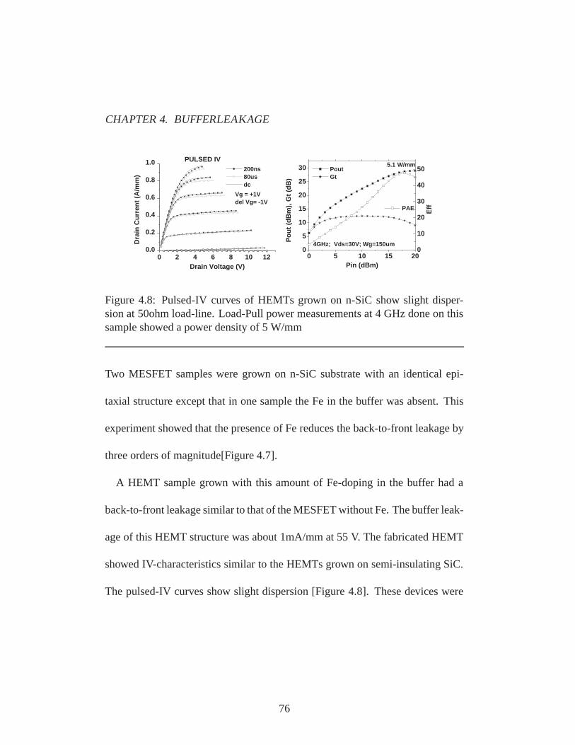
CHAPTER 4. BUFFERLEAKAGE
0 2 4 6 8 10 120.0
0.2
0.4
0.6
0.8
1.0 PULSED IV
Vg = +1Vdel Vg= -1V
Dra
in C
urr
ent
(A/m
m)
Drain Voltage (V)
200ns 80us dc
0 5 10 15 200
5
10
15
20
25
30
Po
ut
(dB
m),
Gt
(dB
)
Pin (dBm)
Pout Gt
0
10
20
30
40
50
4GHz; Vds=30V; Wg=150um
5.1 W/mm
PAE
Eff
Figure 4.8: Pulsed-IV curves of HEMTs grown on n-SiC show slight disper-sion at 50ohm load-line. Load-Pull power measurements at 4 GHz done on thissample showed a power density of 5 W/mm
Two MESFET samples were grown on n-SiC substrate with an identical epi-
taxial structure except that in one sample the Fe in the buffer was absent. This
experiment showed that the presence of Fe reduces the back-to-front leakage by
three orders of magnitude[Figure 4.7].
A HEMT sample grown with this amount of Fe-doping in the buffer had a
back-to-front leakage similar to that of the MESFET without Fe. The buffer leak-
age of this HEMT structure was about 1mA/mm at 55 V. The fabricated HEMT
showed IV-characteristics similar to the HEMTs grown on semi-insulating SiC.
The pulsed-IV curves show slight dispersion [Figure 4.8]. These devices were
76

CHAPTER 4. BUFFERLEAKAGE
-40 -20 0 20 40 60
1µ
10µ
100µ
Bac
kto
Fro
nt
Cu
rren
t (A
)
BackGate Voltage (V)
MOCVD anneal std.RTA anneal
0 20 40 60 80 100 120
0.0
500.0µ
1.0m
1.5m
2.0m
(ohmics without spikes)
Bu
ffer
Lea
kag
e (A
/mm
)
Vds (V)
HEMT on n-SiC
Figure 4.9: Buffer Leakage reduced in HEMTs grown on n-SiC susbstrate bythe removal of spikes in ohmic contacts by using NH3 during the anneal. Thecontacts made on this sample however were not fully ohmic and had slight non-linearity
made with normal gates where the passivation is done after the gate metal de-
position. Power measurements done at 4 GHz yielded a maximum power of
5.1 W/mm at a bias of Vds=30 V [Figure 4.8].
After understanding the effect of ohmic contacts on buffer leakage, the effect
of alloyed ohmic spikes on back-to-front leakage was studied. A HEMT grown
on n-SiC was fabricated by annealing the ohmic contacts in the MOCVD cham-
ber in the presence of ammonia. The back-to-front leakage was compared with
the devices on a control piece annealed by the standard RTA anneal process.
77

CHAPTER 4. BUFFERLEAKAGE
The sample annealed in MOCVD chamber was not ohmic as it was difficult to
obtain ohmic contacts without spikes in a repeatable fashion. The back-to-front
leakage is reduced in the sample that had no spikes in the ohmic contacts as
shown in Figure 4.9. The buffer leakage on this sample also reduced to a value
of 1 mA/mm at 100 V [Figure 4.9].
4.6 Summary
The leakage occuring in the buffer region of the GaN transistors was studied.
The buffer leakage is reduced by increasing the concentration of Fe-flow during
the growth. The spikes in the ohmic contacts were identified as another source
of the buffer leakage. Conducting SiC substrate was tried as the substrate for
growing AlGaN/GaN HEMTs and performance similar to the HEMTs on the
Semi-Insulating SiC substrate was obtained at 4 GHz.
References
[1] A. Chini, D. Buttari, R. Coffie, L. Shen, S. Heikman, A. Chakraborty, S.Keller, and U. K. Mishra, “Power and linearity characteristics of field-platedrecessed-gate AlGaN-GaN HEMTs”. IEEE Electron Device Letters, vol 25,pp 229-231, May 2004.
[2] Y.-F. Wu, A. Saxler, M. Moore, R. P. Smith, S. Sheppard, P. M. Chavarkar, T.
78

CHAPTER 4. BUFFERLEAKAGE
Wisleder, U. K. Mishra, P. Parikh, “30-W/mm GaN HEMTs by field plate op-timization”IEEE Electron Device Letters, vol 25, pp 117-119, March 2004.
[3] Huili Xing, Y. Dora, A. Chini, S. Heikman, S. Keller, U. K. Mishra, “Highbreakdown voltage AlGaN-GaN HEMTs achieved by multiple field plates,”IEEE Electron Device Letters, vol 25, no 4, pp 161-163, April 2004.
[4] Naiqian Zhang , “High Voltage GaN HEMTs with Low on-resistance forSwitching Applications”. PhD thesis, University of California, Santa Bar-bara, 2002.
[5] C. Wetzel, T. Suski, J.W.Ager III, E. R. Weber, E. E. Haller, S. Fischer, B. K.Meyer, R. J. Molnar, P. Perlin, “Pressure induced deep gap state of oxygenin GaN”. Physical Review Letters, vol 78, pp 3923-3926, May 1997.
[6] S. Heikman, S. Keller, S. P. DenBaars, U. K. Mishra,“Growth of Fe dopedsemi-insulating GaN by metalorganic chemical vapor deposition”. AppliedPhysics Letters, vol 81, pp 439-441, July 2002.
[7] C. Poblenz, P. Waltereit, S. Rajan, S. Heikman, U. K. Mishra, J. S.Speck,“Effect of carbon doping on buffer leakage in AlGaN/GaN high elec-tron mobility transistors”. J. Vac. Sci. Technol. B, vol 22(3), pp 1145-1149,May 2004.
[8] X. H. Wu, L. M. Brown, D. Kapolnek, S. Keller, B. Keller, S. P. Den-Baars and J. S. Speck,“Defect structure of metal-organic chemical vapordeposition-grown epitaxial (0001) GaN/Al2O3”, J. Appl. Phys., vol 80(6),pp 3228, Sep 1996.
[9] R. Vetury, N. Q. Zhang, S. Keller, and U. K. Mishra,“The impact of sur-face states on the DC and RF characteristics of AlGaN/GaN HFETs”. IEEEElectron Device Letters, vol 48, pp 560-566, March 2001.
[10] Ilan Ben-Yaacov , “AlGaN/GaN Current Aperture Vertical Electron Transis-tors”. PhD thesis, University of California, Santa Barbara, 2004.
[11] W. Saito, Y. Takada, M. Kuraguchi, K. Tsuda, T. Omura, T. Ogura,“600VAlGaN/GaN power-HEMT: design, fabrication and demonstration on highvoltage DC-DC converter”. Electron Devices Meeting, 2003. IEDM ’03Technical Digest. IEEE International, vol., no.pp. 23.7.1- 23.7.4, 8-10 Dec.2003
79
5Kilo-Volt breakdown voltage devices
and wide periphery devices
5.1 Introduction
The use of multiple field-plates to achieve higher breakdown voltage was
demonstrated in Chapter 2. This chapter presents an improved processing
technique to achieve the effect of multiple field-plates. This processing tech-
nique involves realizing the multiple field-plates as fabricated in a self-aligned
fashion with the gate. This chapter also presents some of the issues identified
in measuring breakdown voltage. Also presented are wide-periphery devices
with high current capacity fabricated by the flip-chip process. The results of the
devices made by the flip-chip process are presented.
80

CHAPTER 5. KILO-VOLT DEVICES
5.2 Trench gate process : Self-aligned field-plates
Chapter 2 showed the use of multiple field-plates in increasing the breakdown
voltage of the devices. In those devices the passivation is done after the gate
and the field-plates were achieved by shifting the gate lithography after each
dielectric deposition step. An improved processing technique, referred as ‘trench
gate process’, was identified which yeilded not only better passivation but also
the ability to obtain field-plates self-aligned with the gate. This improved process
involves doing the SiNx passivation step before the gate step. Trenches defined
by the gate lithography were etched in the SiNx passivation layer using CF4/O2
RIE system. Using the same lithography gate metal was deposited in the trenches
by E-beam evaporation.
5.2.1 Controlling the profile of the trench
The gate lithography was achieved by using a double-layer photoresist (Ap-
pendix C) which yielded a lift-off profile with significant overhang. Due to this
profile of the lithography, the flux reactive ions in the RIE in the normal di-
rection leads to a higher etch rate for the SiNx lying under the opening of the
81

CHAPTER 5. KILO-VOLT DEVICES
1000 1500 2000 2500 3000
-100
-50
0
50
100
150
angledangled direction flux
AFM scan of the trench (trench zoomed-in)
Hei
gh
t (n
m)
Distance (nm)2200 2300 2400 2500 2600
-200
-100
0
100
200AFM scan of the trenchProfile of trench wall in x:y=1:1 scale
Hei
gh
t (n
m)
Distance (nm)
AlGaN
GaN
Source
GaN
SiNx
Dra
in
AlGaN
PR2PR1
Sour
ce
0 1 2 3 4 5
-100
-50
0
50
100
150
SiN
x
SiN
x
dra
in o
hm
ics
sou
rce
oh
mic
s trench
AFM scan of the trench
Hei
gh
t (n
m)
Distance (um)
0.7um
0.3umdouble-layer PhotoResist
Figure 5.1: Schematic of the double layer photoresist used and the AFM scan ofthe trench etched in the SiNx passivation layer.
lithography. The SiNx lying underneath the overhang of the liftoff profile sees a
lower flux of the reactive ions coming at an angle to the normal and hence has a
lower etch rate. This leads to a step-like profile of the etched trench. By varying
the chamber pressure in the RIE the flux of the ions in directions other than the
normal can be varied. Lower pressures (<5 mT) leads to a flux mostly in the
normal direction giving a vertical wall of the etch without any significant etch of
82

CHAPTER 5. KILO-VOLT DEVICES
the SiNx beneath the overhang regions. However it should be noted that at very
low pressures (<2 mT) the etch rate is also significantly reduced and also it is
difficult to obtain a sustainable plasma in RIE3 system at UCSB-Nanofab used
for this experiment. At higher chamber pressures (∼20 mT) there is a significant
flux in the directions other than the normal direction which leads to a significant
etch of the SiNx beneath the overhang regions. This yields a step-like profile of
the etched trench as shown in the AFM scans [Figure 5.1]. These scans were
done by stripping the photoresist after the trench etch to show the profile of the
trench that will be exposed to the metal evaporation.
5.2.2 Controlling the field-plate extension
The gate metal evaporation is done in a E-beam evaporator. The sample is
loaded in a rotating chuck whose surface is kept at an angle to the direction of
the incident metal flux. Since there is an overhang of the liftoff profile of the
photoresist, the angled evaporation enables the gate metal to cover the sidewall
of the etched trenches. This yields a field-plate self-aligned with the gate in
a single process step. By changing the angle of the chuck with respect to the
83

CHAPTER 5. KILO-VOLT DEVICES
Figure 5.2: SEM picture shows the metal evaporated at an angle to the normalon the sample mounted on a rotating chuck. The trench gate metal covers thestep in the etched trench yielding a field-plate self-aligned with the gate.
direction of the incident flux the extension of the self-aligned field-plate could
be changed. For an angle of about 10∼15 degrees and a photoresist height of
1.8µm a field-plate extension of about 0.2µm can be expected. Figure 5.2 shows
an extension of about 0.2µm measured using an SEM.
It should be noted that the angled evaporation done on the sample on a rotating
84

CHAPTER 5. KILO-VOLT DEVICES
chuck leads to a field-plate extension on the source-side too. This contributes to
an increase in the gate-source capacitance leading to a slight reduction in ft and
fmax. One way to avoid the source-side extension is to do metal evaporation on
a chuck at normal angle and then to repeat the evaporation again on a chuck at
an angle oriented towards the drain and without rotation. However this approach
is not suitable to device layouts with interdigitated source-drain fingers where
the source and drain alternately serve two branches in both directions and also
not suitable to any closed geometry devices like circular layouts and winding
gate layouts. However the beneficial effects of the source-side extension of the
field-plate could be understood if one looks at the effect of the surface states in
the source-side on dispersion. The effect of surface states in the source-side on
dispersion is presented in the next section.
5.2.3 The Effect of Source-side dispersion
To study the effect of the surface states in the source-side on dispersion the
effect of surface states in the drain-side needs to be decoupled or removed. A
controlled experiment was performed in which the angle of the evaporation of
85

CHAPTER 5. KILO-VOLT DEVICES
AlGaN
GaN
Source
GaN
drain-side disp.
SiNxGateDrainSource
AlGaN AlGaN
GaN
Source
GaN
source-side disp.
SiNxGateDrainSource
AlGaN AlGaN
GaN
SourceGate
GaN
Trench gate
SiNxGate
DrainSourceAlGaN
0 2 4 6 8 10 12 14 160
200
400
600
800
1k
PULSED IV
MaxVg = 1Vdel Vg= -1V
Dra
in C
urr
ent
(mA
/mm
)
Drain Voltage (V)
200ns 80us dc
0 2 4 6 8 10 12 14 160
200
400
600
800
PULSED IV
MaxVg = 1Vdel Vg= -1V
Dra
in C
urr
ent
(mA
/mm
)
Drain Voltage (V)
200ns 80us dc
0 2 4 6 8 10 12 14 160
200
400
600
800
PULSED IV
MaxVg = 1Vdel Vg= -1V
Dra
in C
urr
ent
(mA
/mm
)
Drain Voltage (V)
200ns 80us dc
Figure 5.3: The schematic of the devices used in the controlled experiment tostudy the effect of source-side dispersion.
the metal for the trench gates were controlled. After etching the trench, metal
evaporation was done on a few dies (shadow masking the rest) with the sample
loaded on a non-rotating chuck with metal flux oriented towards the drian-side.
This yielded devices with dispersion only on source-side. The metal evaporation
was repeated on few other dies (shadow masking the rest) with the sample loaded
on a non-rotating chuck with metal flux oriented towards the source-side. This
yielded devices with dispersion only on the drain-side. The metal evaporation
was repeated on a few other control dies (shadow masking the rest) with the
sample loaded on a rotating chuck with an angle of about 10 degrees to the
86
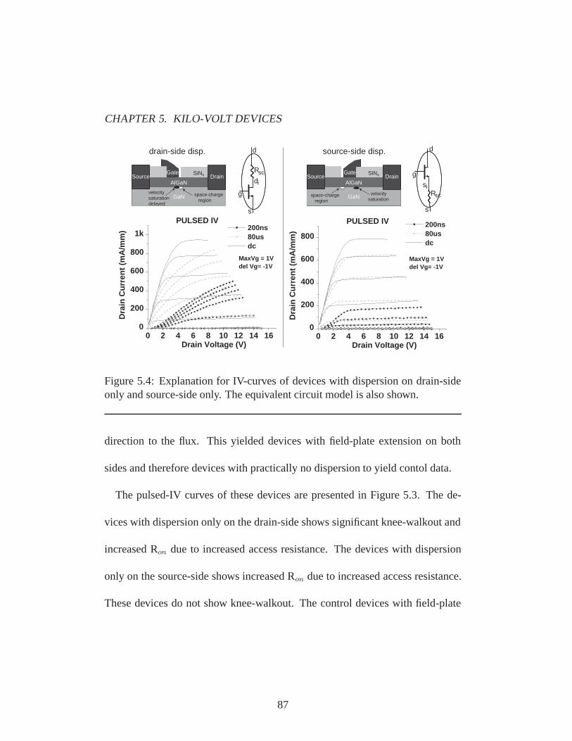
CHAPTER 5. KILO-VOLT DEVICES
AlGaN
GaN
Source
GaN
drain-side disp.
SiNxGateDrainSource
AlGaN
space-charge region
velocity saturationdelayed
AlGaN
GaN
Source
GaN
source-side disp.
SiNxGateDrainSource
AlGaN
space-charge region
velocity saturation
0 2 4 6 8 10 12 14 160
200
400
600
800
1k
PULSED IV
MaxVg = 1Vdel Vg= -1V
Dra
in C
urr
ent
(mA
/mm
)
Drain Voltage (V)
200ns 80us dc
0 2 4 6 8 10 12 14 160
200
400
600
800
PULSED IV
MaxVg = 1Vdel Vg= -1V
Dra
in C
urr
ent
(mA
/mm
)
Drain Voltage (V)
200ns 80us dc
g
s
di
d
Rsc
Rsc
g
s
si
d
Figure 5.4: Explanation for IV-curves of devices with dispersion on drain-sideonly and source-side only. The equivalent circuit model is also shown.
direction to the flux. This yielded devices with field-plate extension on both
sides and therefore devices with practically no dispersion to yield contol data.
The pulsed-IV curves of these devices are presented in Figure 5.3. The de-
vices with dispersion only on the drain-side shows significant knee-walkout and
increased Ron due to increased access resistance. The devices with dispersion
only on the source-side shows increased Ron due to increased access resistance.
These devices do not show knee-walkout. The control devices with field-plate
87
CHAPTER 5. KILO-VOLT DEVICES
extension on both sides have the 200 ns pulsed-IV curves matching the DC-IV
curves.
Current saturation in a Field Effect Transistor is caused by the channel pinch-
off near the gate-drain edge and the velocity saturation of the electrons happen-
ing there. The current gets saturated after this drain voltage which is referred
to as ‘knee voltage’. During dispersion the charging-up of surface states causes
the channel below those surface states to be depleted leading to the formation
of a space-charge region [1]. In a device with drain-side dispersion, this space-
charge region comes between the gate and the drain. The applied drain bias is
partially dropped across this space-charge region leading to lower intrinsic drain
bias. The gate-drain pinch-off is delayed due to the voltage drop at the space-
charge region and is no longer sharp with the applied drain bias. In other words,
the space-charge region in this case leads not only to increased access resistance
but also to the knee-voltage walkout. An equivalent circuit model representing
this is shown in Figure 5.4. In a device with source-side dispersion, this space-
charge region does not come between the gate and the drain. The applied drain
bias, after accomodating the low channel resistance(∼500 ohms-square), is seen
by the channel below the gate. This leads to sharp gate-drain pinch-off and hence
88

CHAPTER 5. KILO-VOLT DEVICES
an abrupt knee voltage. The space-charge region appears between the gate and
the source causing an increased source access resistance and a reduced gm. In
other words, the space-charge region in this case leads only to the increased ac-
cess resistance but not to the knee-voltage walkout. An equivalent circuit model
representing this is shown in Figure 5.4.
This controlled experiment shows that the surface states on the source-side
contribute to the increase in access resistance. If a slight reduction of frequency
can be tolerated it would be beneficial to have field-plate extension on the source-
side too.
5.2.4 Frequency response of the trench-gates
The small signal performance of the devices with trench gates are presented in
Figure 5.5. These devices had field-plate extension on both sides. The measured
ft and fmax of these devices are 18.5 GHz and 64 GHz. The pulsed-IV mea-
surements performed at loadline of 50ohms showed no dispersion. The pulsed-
IV measurements done at a higher loadline of 165ohms also showed insignifi-
cant dispersion [Figure 5.5]. The load-pull power measurements done at 4 GHz
89

CHAPTER 5. KILO-VOLT DEVICES
100M 1G 10G 100G0.1
1
10
100
ft=18.5 GHz
fmax
=64 GHz
Mag
nit
ud
e
Frequency (Hz)
|h21||U|
0 5 10 15 20 25 300
200
400
600
800
1kpulsed IV curves
MaxVg = 1Vdel Vg= -1V
Dra
in C
urr
ent
(mA
/mm
)
Drain Voltage (V)
200ns 50ohmLL 200ns 165ohmLL dc
Figure 5.5: Small signal measurements show an ft=18.5 GHz and fmax=64 GHz.The large signal 200 ns pulsed-IV measurements show no dispersion at 50 ohms.At a higher loadline of 165 ohms there is little dispersion.
yielded a power density of 6.7 W/mm and a power-added-efficiency of 64% at a
bias of 35 V [Figure 5.6]. This is comparable to the values (6.3 W/mm) reported
by Chini et al. at a bias of 30 V [2]. At a higher drain bias of 55 V the de-
vice yielded a power density of 8.8 W/mm and power-added-efficiency of 48%
[Figure 5.6].
90
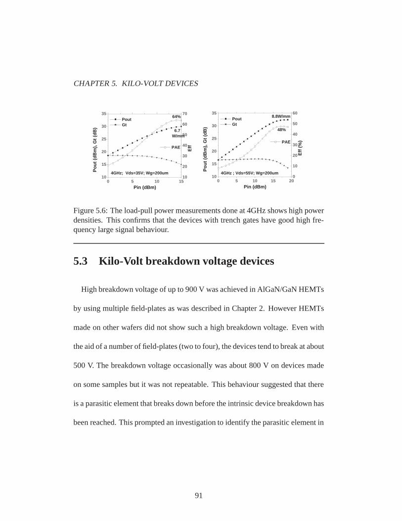
CHAPTER 5. KILO-VOLT DEVICES
0 5 10 1510
15
20
25
30
35
Po
ut
(dB
m),
Gt
(dB
)
Pin (dBm)
Pout Gt
10
20
30
40
50
60
70
4GHz; Vds=35V; Wg=200um
6.7W/mm
64%
PAE
Eff
0 5 10 15 2010
15
20
25
30
35
48%
8.8W/mm
Po
ut
(dB
m),
Gt
(dB
)
Pin (dBm)
Pout Gt
0
10
20
30
40
50
60
4GHz ; Vds=55V; Wg=200um
PAE
Eff
(%
)
Figure 5.6: The load-pull power measurements done at 4GHz shows high powerdensities. This confirms that the devices with trench gates have good high fre-quency large signal behaviour.
5.3 Kilo-Volt breakdown voltage devices
High breakdown voltage of up to 900 V was achieved in AlGaN/GaN HEMTs
by using multiple field-plates as was described in Chapter 2. However HEMTs
made on other wafers did not show such a high breakdown voltage. Even with
the aid of a number of field-plates (two to four), the devices tend to break at about
500 V. The breakdown voltage occasionally was about 800 V on devices made
on some samples but it was not repeatable. This behaviour suggested that there
is a parasitic element that breaks down before the intrinsic device breakdown has
been reached. This prompted an investigation to identify the parasitic element in
91
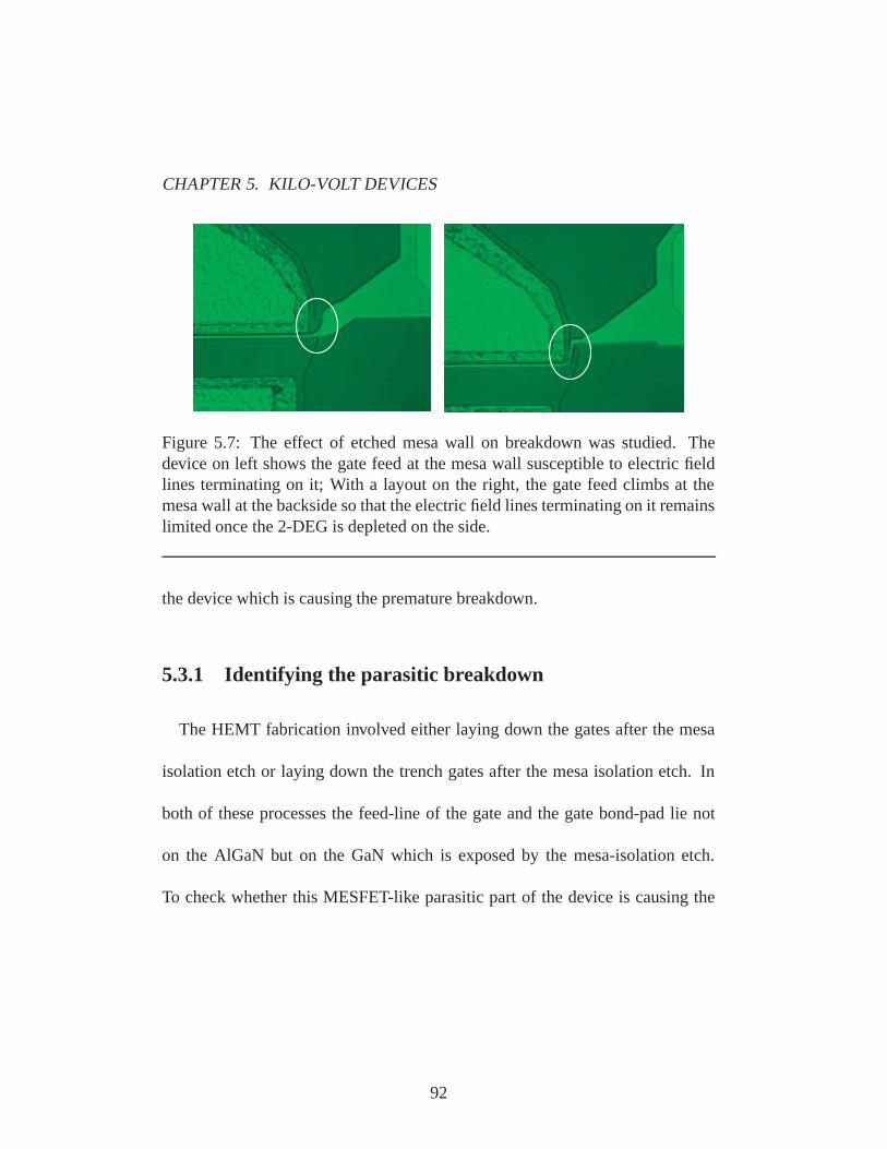
CHAPTER 5. KILO-VOLT DEVICES
Figure 5.7: The effect of etched mesa wall on breakdown was studied. Thedevice on left shows the gate feed at the mesa wall susceptible to electric fieldlines terminating on it; With a layout on the right, the gate feed climbs at themesa wall at the backside so that the electric field lines terminating on it remainslimited once the 2-DEG is depleted on the side.
the device which is causing the premature breakdown.
5.3.1 Identifying the parasitic breakdown
The HEMT fabrication involved either laying down the gates after the mesa
isolation etch or laying down the trench gates after the mesa isolation etch. In
both of these processes the feed-line of the gate and the gate bond-pad lie not
on the AlGaN but on the GaN which is exposed by the mesa-isolation etch.
To check whether this MESFET-like parasitic part of the device is causing the
92

CHAPTER 5. KILO-VOLT DEVICES
breakdown, the etched mesa regions were filled with SiOx dielectric. This was
done by the E-beam evaporation of SiOx after the mesa isolation etch. The evap-
oration was done by a liftoff process using the same mesa lithography in a self-
aligned fashion. This change in the process did not lead to an improvement in the
breakdown voltage. This confirms that the feed regions are not causing the pre-
mature breakdown. This also confirms the expectation that the peak electric field
on the gate feed line should be low because the GaN beneath it is un-itentionally
doped. This UID-GaN has almost no carriers and the depletion region has to be
quite wide leading to low electric field peak at the feed line.
The HEMT process used involves using mesa etch for device isolation. The
gate feed runs in the etched regions and climbs over the wall of the mesa to con-
tinue as the gate in the active region of the device. The wall of the mesa where
the gate feed climbs over was suspected as a possible cause of premature break-
down. In order to reduce the magniturde of the electric field lines terminating
on the gate feed at the mesa wall, the gate feed was made to climb over the wall
far behind the active region of the device as shown in Figure 5.7. By doing this
though there was improvement on some devices (up to Vbr=800 V), the break-
down voltage was not uniform over many devices and the devices would not
93
CHAPTER 5. KILO-VOLT DEVICES
reach 1 kV even with four field-plates.
The air which surrounds the fabricated device during the breakdown volt-
age measurements was suspected to be triggerring the breakdown beyond a
certain drain voltage. A study of various high breakdown voltage measure-
ments that have been reported in the literature was done. Those devices with
more than a 1 kV breakdown voltage predominantly have vertical geometry
in which the drain is in the back side of the substrate (various DMOS struc-
tures). In these devices the semiconductor itself is the dielectric between elec-
trodes at vastly different potentials [3]. Devices on Si with lateral geometry that
have been reported with very high breakdown voltage have large source-drain
spacing(>70µm) [4][5]. However all the lateral geometry devices on a high
bandgap material like SiC have been reported to have been tested with Fluorinert,
though it is never stated why it is so [6]. Testing the fabricated AlGaN/GaN
HEMTs immersed in the inert liquid called Fluorinert (FC-77) showed that the
devices could withstand more than a 1 kV on the drain. These breakdown voltage
results were consistent and reproducible.
94
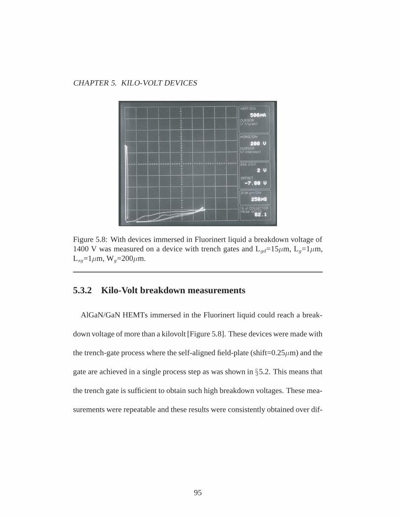
CHAPTER 5. KILO-VOLT DEVICES
Figure 5.8: With devices immersed in Fluorinert liquid a breakdown voltage of1400 V was measured on a device with trench gates and Lgd=15µm, Lg=1µm,Lsg=1µm, Wg=200µm.
5.3.2 Kilo-Volt breakdown measurements
AlGaN/GaN HEMTs immersed in the Fluorinert liquid could reach a break-
down voltage of more than a kilovolt [Figure 5.8]. These devices were made with
the trench-gate process where the self-aligned field-plate (shift=0.25µm) and the
gate are achieved in a single process step as was shown in §5.2. This means that
the trench gate is sufficient to obtain such high breakdown voltages. These mea-
surements were repeatable and these results were consistently obtained over dif-
95

CHAPTER 5. KILO-VOLT DEVICES
0 5 10 15 200
200
400
600
800
1000
1200
1400
1600
1800
2000
Vbr = (86.7 * Lgd) - 3.7
Vb
r (V
)
Lgd (um)
Trenchgates withFTrenchgates withoutFBeforepassiv withF
0 400 800 1200 1600 20000.0
5.0m
10.0m
15.0m
20.0m
OFF-state IV curves
Cu
rren
t (A
)
Voltage (V)
Vgs = -7V to -1VdelVgs = +2V
Figure 5.9: The breakdown voltage versus Lgd measured with and without Fluo-rinert at various process steps. Lsg=1µm; Lg=1µm; Wg=200µm.
ferent processing runs. Furthermore, the breakdown voltage increased linearly
with increasing gate-drain spacing.
5.4 What is limiting the breakdown voltage ?
Gate leakage was thought to be critical and limiting the breakdown voltage
as reported by Zhang et al. [7]. Based on that work it was believed that the
presence of a gate dielectric is critical to achieve a kilo-volt breakdown voltage
in AlGaN/GaN HEMTs. But it is shown in this work that even for high gate
96

CHAPTER 5. KILO-VOLT DEVICES
leakage values of 1 mA/mm, a kilo-volt was obtained with trench gates and with
device immersed in Fluorinert.
To explain the high breakdown voltage results and to study the limits of break-
down voltage in AlGaN/GaN HEMTs a device fabrication run was carried out in
which the breakdown voltage was monitored in the presence of Fluorinert after
each process step. The breakdown voltage of devices before passivation mea-
sured in the presence of Fluorinert followed a linear increase with Lgd spacing
[Figure 5.9]. Without fluorinert the breakdown voltage was limited to a maxi-
mum of about 400∼500 V. After passivation the breakdown voltage measured
in the presence of Fluorinert showed a reduced breakdown voltage to which the
presence or absence of fluorinert did not make a difference. After passivation
the devices with trench gates measured with Fluorinert showed a linear increase
in breakdown voltage [Figure 5.9]. Without Fluorinert the breakdown voltage in
these devices gets clamped around 500 V [Figure 5.9].
The results of this experiment can be summarized as follows. If the peak
electric field is not alleviated the devices break early whether they are in the
presence of air or fluorinert. If the peak electric field at the drain edge of the gate
is alleviated either by surface states before passivation or by the using the trench
97

CHAPTER 5. KILO-VOLT DEVICES
gates which provide an integrated field-plate, the breakdown follows a linear
trend as shown in linear fit in Figure 5.9. From this linear trend, supposing that
the electric field is constant between the gate and drain an electric field strength
of 86 V/µm∼0.86 MV/cm could be calculated. Given that the breakdown field
strength of GaN is about 3 MV/cm, these devices could be at the inherent limits
of the material system involved.
To determine if the parasitic breakdown of the Fluorinert liquid is yielding this
linear trend, metal pads with varying spacings were deposited on an insulating
sapphire substrate. In the presence of Fluorinert, the metal pads could be biased
to 1600 V for a 4µm spacing and more than 2000 V for spacings greater than
7µm. The breakdown voltages of the devices with these spacings [Figure 5.9]
are much lower than these numbers, thereby eliminating the parasitic breakdown
of Fluorinert. The linear trend in the results could be due to the depletion region
extending and reaching the drain contacts [8]. As seen in §4.3, the Fe-doping
level seems to change the slope of the Vbr vs. Lgd. The linear trend in the results
could also be possible if the Fe-doped buffer underneath the device is reaching
its limits of insulating behaviour.
A controlled experiment was done to see the effect of Lsg spacing on break-
98
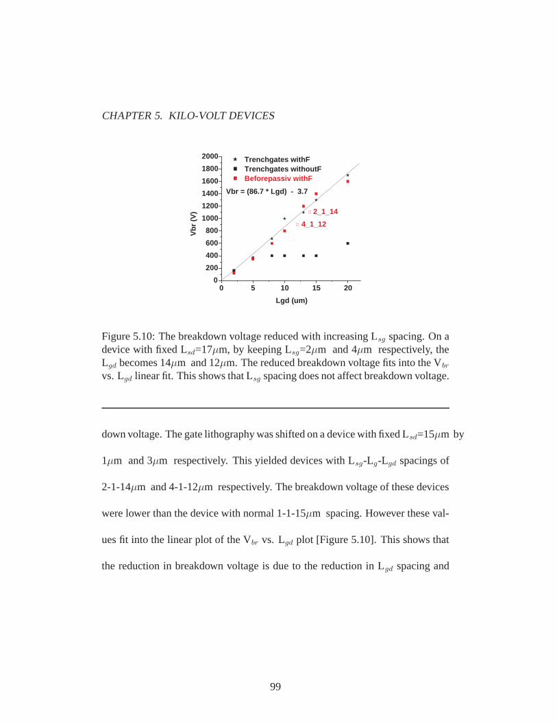
CHAPTER 5. KILO-VOLT DEVICES
0 5 10 15 200
200
400
600
800
1000
1200
1400
1600
1800
2000 Trenchgates withFTrenchgates withoutFBeforepassiv withF
4_1_12
2_1_14
Vbr = (86.7 * Lgd) - 3.7V
br
(V)
Lgd (um)
Figure 5.10: The breakdown voltage reduced with increasing Lsg spacing. On adevice with fixed Lsd=17µm, by keeping Lsg=2µm and 4µm respectively, theLgd becomes 14µm and 12µm. The reduced breakdown voltage fits into the Vbr
vs. Lgd linear fit. This shows that Lsg spacing does not affect breakdown voltage.
down voltage. The gate lithography was shifted on a device with fixed Lsd=15µm by
1µm and 3µm respectively. This yielded devices with Lsg-Lg-Lgd spacings of
2-1-14µm and 4-1-12µm respectively. The breakdown voltage of these devices
were lower than the device with normal 1-1-15µm spacing. However these val-
ues fit into the linear plot of the Vbr vs. Lgd plot [Figure 5.10]. This shows that
the reduction in breakdown voltage is due to the reduction in Lgd spacing and
99
CHAPTER 5. KILO-VOLT DEVICES
the increase in the Lsg spacing did not affect breakdown voltage.
An experiment to probe this issue further was done in which the fabricated
device was covered with 1µm thick dielectric (ICP deposited SiOx). Covering
the device with this dielectric showed no change in the breakdown voltage in the
presence of Fluorinert, indicating that an appropriate passivation to ultimately
eliminate the need for Fluorinert needs to be pursued.
5.5 Wide periphery devices
Devices with wide-periphery and hence large current capacity were made to
do switching measurements in an actual power converter-like environment and
also to eventually incorporate them into a switched power converter module. The
first generation devices had a linear geometry with 1∼2 mm wide active region.
Many such devices were wirebonded to get a wider device (up to 5.5 mm wide)
with a current capacity of 5 A. However combining such discrete devices by
wirebonding posed difficulties. The reliability of the wirebonds was an issue
and the access resistance was limited by the wirebonds themselves.
In the next generation devices, twenty short (500µm) device fingers were
100

CHAPTER 5. KILO-VOLT DEVICES
Figure 5.11: Wide periphery(10mm) device with interdigitated fingers. Thesource fingers get connected during the flip-chip bonding.
made adjacent to each other. The drain contacts of the fingers were tied together
at one side. The interdigitated gate feeds of the fingers were tied at the opposite
side. The source fingers were brought out at the gate feed side to be connected.
The source connections need to be made by crossing over the gate feeds either
by dielectric/air bridges or by external connections like wirebonds or flip-chip
bonding. The bond pads on source and drain contacts were made of 6µm thick
Au deposited by Ebeam. The contact patterns on the flip-chip substrate also had
101

CHAPTER 5. KILO-VOLT DEVICES
6µm thick Au pads which after bonding leads to 12µm thick metal connections.
The details for the flip-chip process are given in apendix-C. The flip-chip process
has an additional advantage in that the flip-chip substrate provides an additional
heat sink to the device [9]. Also if AlGaN/GaN HEMTs were grown on cheaper
substrates like Si which has low thermal conductivity, doing a flip-chip bond of
the device onto a substrate with higher thermal conductivity would enhance the
thermal budget of the device. Also since the flip-chip substrate gives mechan-
ical support the original substrate could be lapped and thinned to enhance the
thermal conduction if a double-sided heat sink were implemented.
The layout used for the flip-chip devices is show in Figure 5.11. The source
and drain pad lengths were intentionally kept longer (about 50µm) because of
the alignment tolerance of the flip-chip bonder at UCSB-Nanofab which is +/-
10µm. This increased the die area by a large factor. If the bondpad dimensions
were optimized it would lead to reduction in the die size by atleast four times.
The actual die area of the completed device is shown in Figure 5.11. The device
has 20 interdigitated fingers of 500µm width contributing to a total width of
10 mm and hence a current capacity of 10 A. The electrodes are brought out
into wide area metal pads which enable easy wirebonding. These pads are wide
102
CHAPTER 5. KILO-VOLT DEVICES
enough so that the device can be soldered directly to the contacts of a switching
test set-up or a power converter module. Many such compact modules could be
put together to achieve higher current capacity.
5.6 Summary
The chapter presents improvements in the processing of high breakdown volt-
age devices and in the high voltage measurements. The trench gate technol-
ogy was observed to have advantages over the standard process for AlGaN/GaN
HEMTs. It also allows for obtaining field-plates self-aligned with the gate in
a single process step. The parasitic breakdown voltage which was causing the
device to break prematurely was identified. Using Fluorinert liquid breakdown
voltages of up to 1900 V was measured on AlGaN/GaN HEMTs. Possible rea-
sons which could explain the linear increase of breakdown voltage with Lgd
spacing was discussed. Wide periphery devices with large current capacity were
made. These devices were improved by using the flip-chip technology.
103
CHAPTER 5. KILO-VOLT DEVICES
References
[1] Robert Coffie , “Characterizing and Suppressing DC-to-RF Dispersion inAlGaN/GaN High Electron Mobility Transistors”. PhD thesis, University ofCalifornia, Santa Barbara, 2003.
[2] A. Chini, D. Buttari, R. Coffie, L. Shen, S. Heikman, A. Chakraborty, S.Keller, and U. K. Mishra, “Power and linearity characteristics of field-platedrecessed-gate AlGaN-GaN HEMTs”. IEEE Electron Device Letters, vol 25,pp 229-231, May 2004.
[3] A. K. Agarwal, J. B. Casady, L. B. Rowland, S. Seshadri, R. R. Siergiej, W.F. Valek, C. D. Brandt,“700-V asymmetrical 4H-SiC gate turn-off thyristors(GTO’s),”.Electron Device Letters, IEEE, vol.18, no.11pp.518-520, Nov 1997
[4] S. Merchant, E. Arnold, H. Baumgart, R. Egloff, T. Letavic, S. Mukherjee,H. Pein,“Dependence of breakdown voltage on drift length and buried ox-ide thickness in SOI RESURF LDMOS transistors,”. Power SemiconductorDevices and ICs, 1993. ISPSD ’93. Proceedings of the 5th International Sym-posium on, pp.124-128, 18-20 May 1993.
[5] S. Hardikar, R. Tadikonda, D. W. Green, K. V. Vershinin, E. M. S.Narayanan,“Realizing high-voltage junction isolated LDMOS transistors withvariation in lateral doping,”. Electron Devices, IEEE Transactions on , vol.51,no.12pp. 2223- 2228, Dec. 2004.
[6] J. Spitz, M. R. Melloch, J. A. Cooper, Jr., M. A. Capano,“2.6 kV 4H-SiClateral DMOSFETs,”. Electron Device Letters, IEEE, vol.19, no.4pp.100-102,Apr 1998.
[7] Naiqian Zhang , “High Voltage GaN HEMTs with Low on-resistance forSwitching Applications”. PhD thesis, University of California, Santa Barbara,2002.
[8] W. R. Frensley,“Power-limiting breakdown effects in GaAs MESFET’s,”Electron Devices, IEEE Transactions on , vol.28, no.8, pp. 962- 970, Aug1981.
[9] Jian Xu , “AlGaN/GaN High-Electron-Mobility-Transistors Based Flip-chipIntegrated Broadband Power Amplifiers”. PhD thesis, University of Califor-nia, Santa Barbara, 2000.
104
6Switching measurements
6.1 The need for switching measurements
AlGaN/GaN HEMTs with high breakdown voltages have been demon-
strated in Chapters 2 and 5. The breakdown versus speed trade-off is
overcome by using field-plates. Using the trench gate process technology, break-
down voltage of kilovolt has been demonstrated. Small signal measurements of
devices made with this technology and with a Lg=0.7µm showed an ft=18.5 GHz
and fmax=64 GHz [Chapter 5].
To characterize the devices for large signal response, pulsed-IV with pulse-
width upto 200 ns were done. The pulsed-IV measurements were done at a
50 ohm load-line upto a bias of 15 V and at a 165 ohm load-line upto a bias
of 30 V. For measurements done at 165 ohm load-line the pulsed-IV showed
105
CHAPTER 6. SWITCHING MEASUREMENTS
increased dispersion compared to the 50 ohm measurement though still insignif-
icant [Chapter 5]. So it is expected that the pulsed-IV done at larger load-
lines typical in switching application may show greater dispersion. However
microwave power measurements at 4GHz done on devices with trench gates
(Lg=0.7µm) showing a power density of 8.8 W/mm for a Vds bias of 55 V [Chap-
ter 5] indicate that this may not be excessive.
Devices with large breakdown voltages operate at a much higher load-lines.
These load-lines are usually not purely resistive. For example, in a switched
power converter the switching device is subjected to inductive and capacitive
loading which leads to non-linear load-lines. To characterize the frequency re-
sponse of the devices with large breakdown voltages, larger load-lines are needed
and dc-power supplies with larger voltage and power capacities are needed. The
standard pulsed-IV measurement system could not be used because the dc-power
supply used could only go upto 60 V and it could accomodate only resistive load-
lines. So the best means to characterize these devices is to have a switching test
system imitating the load-lines and the waveforms that the device sees in an ac-
tual switching application. This is achieved by having a two-pulse switching
setup with inductive load [1][2]. During the first pulse the inductor is charged
106

CHAPTER 6. SWITCHING MEASUREMENTS
IindId
Isw
Vgs
Iind
Isw
Id
Turnon
Turnoff
char
ging
freew
heel
ing
on-s
tate
off-s
tate
waveforms time
Figure 6.1: Schematic of the switching test set-up and the waveforms duringdifferent phases of the double-pulse signal
with a certain current which is made to free-wheel in a diode. During the second
pulse the device under test is subjected to this current. The transient response of
the device to this current gives a measure of the high frequency performance of
the device.
107

CHAPTER 6. SWITCHING MEASUREMENTS
6.2 Switching setup schematic and waveforms
A schematic of the test setup is shown in Figure 6.1. An inductive load is
added in series to the switch under test. A free-wheeling diode is connected
in parallel to the inductive load to bypass the current in the inductor when the
device is in the off-state. A Gate drive circuit controls the Vgs voltage. The
switching measurements were done with the help of Dr. Sriram Chandrasekaran
and Dr. Vivek Mehrotra at Rockwell Scientific, Thousand Oaks.
The various waveforms of the double-pulse switching measurement is as shown
in Figure 6.1. In the begining the switch is kept off and the applied dc-bias ap-
pears across the device. There is no current in the circuit. When the gate is first
turned on during the charging period, the switch conducts (Isw) and the volt-
age across the device (Vsw) drops. As the difference in voltage appears across
the inductor the inductor current increases continuously. When the switch is
turned-off in the free-wheeling period the current in the inductor is pushed into
the free-wheeling diode. The voltage across the switch in this period is the sum
of Vdc and Vdiode−drop. The forward voltage drop of the diode (∼0.7V) appears
across the inductor and the inductor current falls off slowly. When the switch is
108

CHAPTER 6. SWITCHING MEASUREMENTS
turned on again in the on-state period, the inductor current is taken by the switch
and voltage across the device falls to Von. Thus a current which was originally
established in the circuit is switched by the device from another branch of the
circuit to itself. This transistion which imitates the actual transition in a power
converter is defined as ’turn-on’.
The diode gets reverse biased and undergoes reverse recovery. The current
for the reverse recovery passes through the switch. The difference between the
Vdc and Von of the device appears across the inductor and the inductor current
continuously increases from its original value. At the off-state period the switch
is turned-off and the voltage across the switch increases. After the voltage across
the switch reaches the sum of Vdc and Vdiode−drop, the diode turns on and the
current in the inductor is bypassed into the branch of the circuit with the diode.
This transition, defined as ’turn-off’, imitates the actual power converter where
the current through the switch is sent into another branch when the switch is
turned-off. The inductor current being opposed by the diode-drop slowly decays
to zero.
109

CHAPTER 6. SWITCHING MEASUREMENTS
100 V / 570 mA TURN-ON
Time (µs)0.3 0.4 0.5 0.6 0.7 0.8 0.9 1.0 1.1 1.2
Vgs
and
Vds
(V)
0
20
40
60
80
100
120
Id (mA
)
0
100
200
300
400
500
600
700Vds Id
Vgs
100 V / 570 mA TURN-OFF
Time (µs)0.4 0.6 0.8 1.0 1.2 1.4 1.6
Vgs
and
Vds
(V)
0
50
100
150
Id (mA
)
-200
0
200
400
600
800
Vds
Id
Vgs
Figure 6.2: The need for compact test setup. Devices probed on dc-probestationshowed a lot of ringing. The turn-on and turn-off characterisitic of a 2 mm widedevice with two field-plates and Lg=1.5µm, Lgd=15µm.
6.3 The need for compact test setup
The preliminary switching measurements were done on devices made with
multiple field plates as described in Chapter 2. These devices did not have large
bondpads and the bondpads would peel-off during the wirebonding process. So
these devices were probed on-wafer with the dc-probe station needles that were
connected by bnc-cables to the test setup. These measurements showed a lot of
ringing due to the parasitics involved in the probing process. The waveforms of
the devices measured in this way is shown in Figure 6.2. The gate pulse did not
have fast transitions (turn-on duration was about 0.5µs) due to the parasitics of
the cables and probes.
110
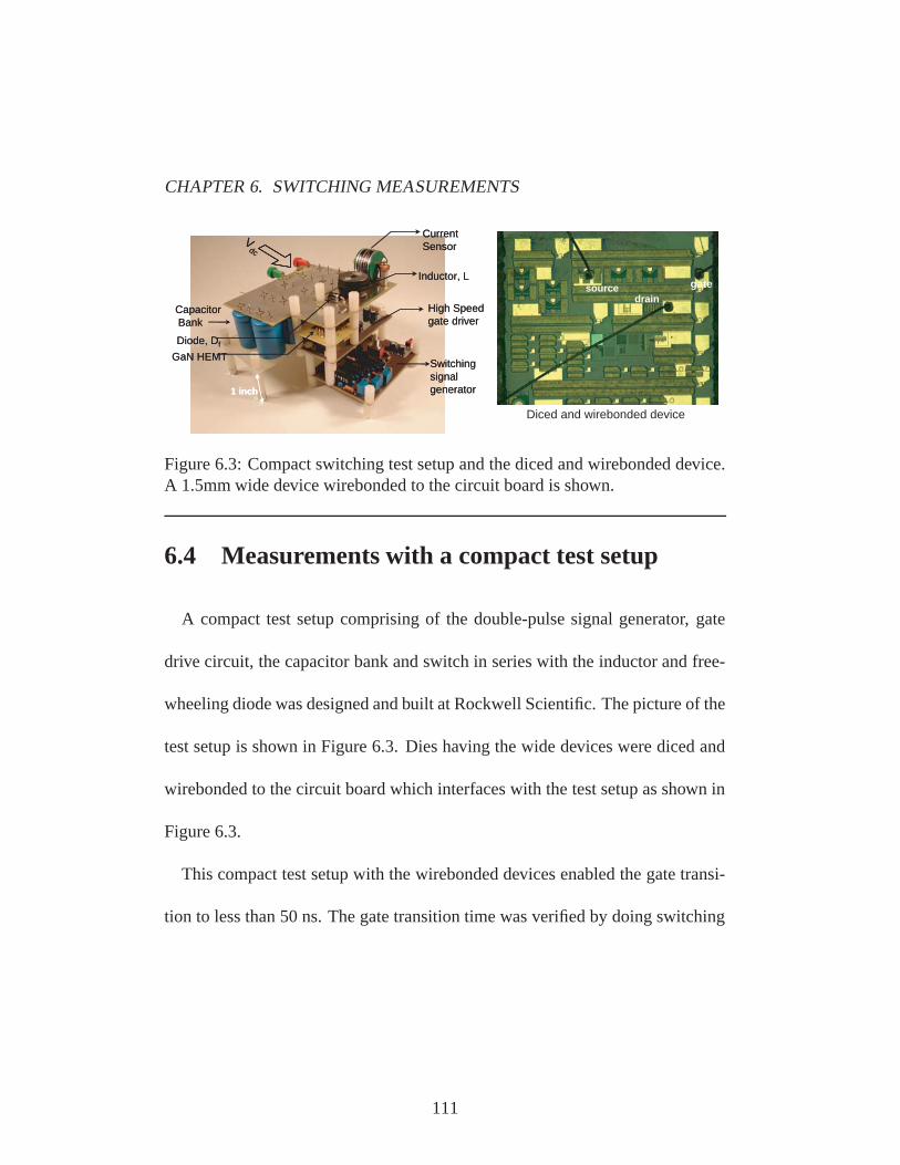
CHAPTER 6. SWITCHING MEASUREMENTS
CapacitorBank
Inductor, L
GaN HEMTDiode, Df
High Speed gate driver
Vdc
Switching signal generator
Current Sensor
1 inch
CapacitorBank
Inductor, L
GaN HEMTDiode, Df
High Speed gate driver
Vdc
Switching signal generator
Current Sensor
1 inch
sourcedrain
gate
Diced and wirebonded device
Figure 6.3: Compact switching test setup and the diced and wirebonded device.A 1.5mm wide device wirebonded to the circuit board is shown.
6.4 Measurements with a compact test setup
A compact test setup comprising of the double-pulse signal generator, gate
drive circuit, the capacitor bank and switch in series with the inductor and free-
wheeling diode was designed and built at Rockwell Scientific. The picture of the
test setup is shown in Figure 6.3. Dies having the wide devices were diced and
wirebonded to the circuit board which interfaces with the test setup as shown in
Figure 6.3.
This compact test setup with the wirebonded devices enabled the gate transi-
tion to less than 50 ns. The gate transition time was verified by doing switching
111

CHAPTER 6. SWITCHING MEASUREMENTS
ton50nsVds
Vgs
toff30ns
Vds
Vgs
Figure 6.4: Gate turn-on and turn-off times verified by resistive loading.Vdc=150 V, Rload=560 ohms, Vgon=2 V, Vgoff=-11 V
measurements on the device under resistive loading. A 1mm wide device with
Lg=1.5µm, Lgd=15µm with two field-plates was used in this measurement. The
turn-on and turn-off characteristic with resistive loading is shown in Figure 6.4.
The turn-on gate pulse changes in less than 50 ns and the turn-off gate pulse
changes in less than 30 ns.
Switching measurements were then done with inductive loading. An induc-
tor of 680µH was used to charge the circuit with current and a Si p-i-n diode
(MUR1100E) was used as the free-wheeling diode. A device with Wg=1 mm,
Lg=1.5µm, Lgd=15µm and two field-plates was used as the switch for this mea-
surement. The waveforms captured during the duration of the double pulse is
112

CHAPTER 6. SWITCHING MEASUREMENTS
Turn OFFTurn ON
Reverse recovery
charging
800mA
charging
vg
vsw
isw
Vonincrease
Figure 6.5: Switching measurements with compact test setup and inductive load-ing. Wg=1 mm, Lg=1.5µm, Vdc=120 V, Lload=680 µH, Vgon=2V, Vgoff =-11 V
shown in Figure 6.5.
The switch conducts current during the initial charging period. When the
switch is turned off the current through the switch drops to zero and the inductor
current is bypassed by the free-wheeling diode. When the switch is turned on
again, the current in the free-wheeling circuit is drawn by the device and the Vsw
drops driving the diode into reverse bias. The reverse bias depletion region of
the diode is setup by the reverse recovery current which is carried by the device.
113

CHAPTER 6. SWITCHING MEASUREMENTS
Vgs=2v to -10v
Isw=2.4A
Vsw=150v
Vgs=2v to -10v
Isw=2.4A
Vsw=150v
20ns
Figure 6.6: High current turn-off characteristic shows a turn-off time less than20 ns, which is still limited by the gate transition speed. Wg=5.5 mm, Lg=1.5µm,Vdc=150 V, Lload=680µH, Vgon=2 V, Vgoff =-11 V
The sharp peak observed in the current at turn-on is due to the reverse recovery
of the diode. Once the reverse depletion region of the diode has been setup, the
reverse recovery component of the current goes to zero. The current thereafter
carried by the switch is the current that was free-wheeling in the diode. The
voltage drop in the inductor continues to increase the current in the switch in
the on-state period. When the device is turned-off the current through the device
goes to zero and the current setup in the inductor starts to free-wheel through the
114

CHAPTER 6. SWITCHING MEASUREMENTS
diode.
From the waveforms, turn-on and turn-off times of about 25 ns were observed.
The on-state voltage drop across the device was higher than expected. Also the
Von increased with increasing current in the device as seen in Figure 6.5. §
6.5.2 discusses the possible reasons for the high values of Von observed in the
switching measurements.
Switching measurements were also perfomed on devices with high current
capacity. Three devices in a die were wirebonded together to achieve a 5.5 mm
wide device with a peak current capacity of 5 A. These devices switched a cur-
rent of 2.4 A at a Vdc=150 V. The turn-off characterisitic is shown in Figure 6.6.
The turn-off time was less than 20 ns. The gate transition time was about 20 ns.
This shows that the switching speed is still limited by the gate transition and not
by the intrinsic performance of the switch.
115
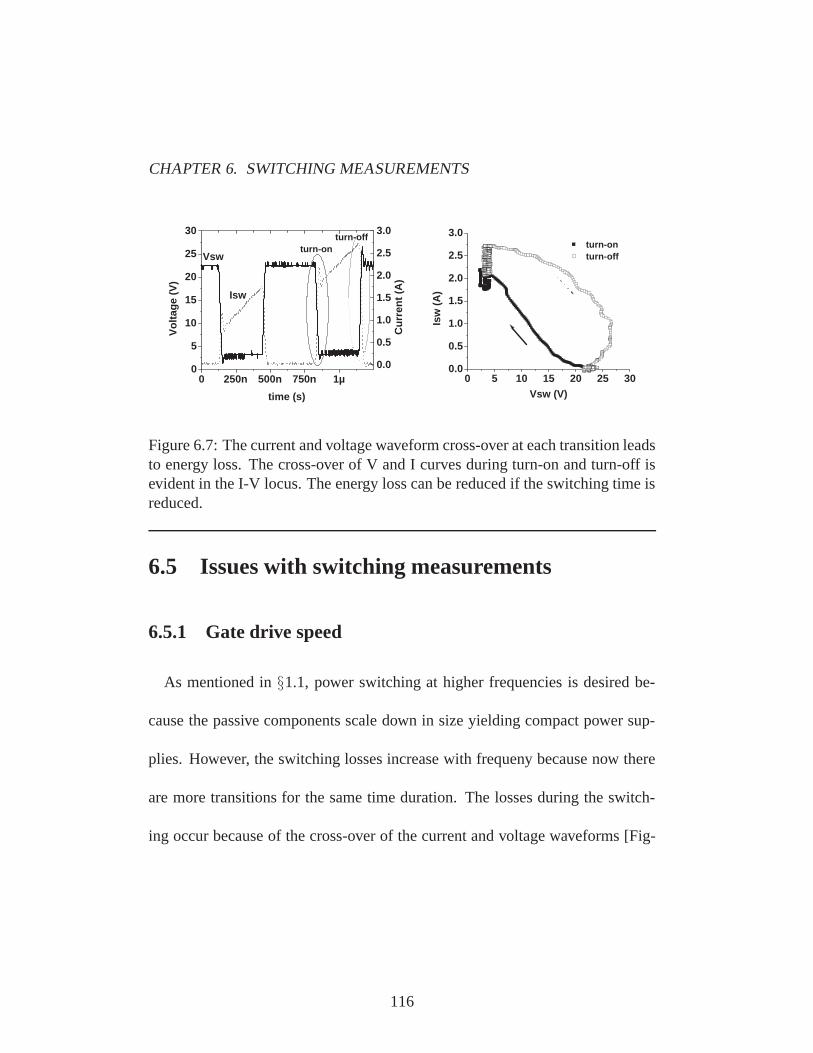
CHAPTER 6. SWITCHING MEASUREMENTS
0 250n 500n 750n 1µ0
5
10
15
20
25
30turn-off
turn-on
Isw
Vsw
Vo
ltag
e (V
)
time (s)
0.0
0.5
1.0
1.5
2.0
2.5
3.0
Cu
rren
t (A
)
0 5 10 15 20 25 300.0
0.5
1.0
1.5
2.0
2.5
3.0
Isw
(A
)
Vsw (V)
turn-onturn-off
Figure 6.7: The current and voltage waveform cross-over at each transition leadsto energy loss. The cross-over of V and I curves during turn-on and turn-off isevident in the I-V locus. The energy loss can be reduced if the switching time isreduced.
6.5 Issues with switching measurements
6.5.1 Gate drive speed
As mentioned in §1.1, power switching at higher frequencies is desired be-
cause the passive components scale down in size yielding compact power sup-
plies. However, the switching losses increase with frequeny because now there
are more transitions for the same time duration. The losses during the switch-
ing occur because of the cross-over of the current and voltage waveforms [Fig-
116

CHAPTER 6. SWITCHING MEASUREMENTS
Figure 6.8: The schematic block diagram of the gate drive circuit used in thecompact switching test setup.
ure 6.7]. The energy loss in each switching transistion is given by integrating
i(t)×v(t) product with time. To minimize the switching losses the turn-on and
turn-off times should be kept as low as possible [3][4]. As observed in the mea-
surements described in the previous section the switching speed is limited by the
transition time of the gate drive circuit.
The gate driver used for power switching at higher frequency should also be
capable of driving the gate as fast as possible. The schematic of the compact gate
117

CHAPTER 6. SWITCHING MEASUREMENTS
driver circuit used at Rockwell Scientific is shown in Figure 6.8. The double-
pulse signals are generated by a monostable multi-vibrator circuit. The double-
pulse signal is coupled by an opto-coupler to an isolated dc-supply for the driver.
The opto-coupler also serves to shift the signal levels. The driver consists of a
current buffer which is made of npn and pnp structure connected as shown in
Figure 6.8. When the gate voltage needs to be increased the npn transistor at the
top is turned-on while the pnp transistor at the bottom is turned-off thus causing
the gate to charge up. When the gate voltage needs to be decreased the above
process is reversed.
In order to increase the gate drive speed the a faster optocoupler needs to
be used. Or in the place of the optocoupler a faster galvanic isolator can be
used. Increasing the slew rate of the transistors in the current buffer would also
improve the gate drive speed.
6.5.2 High Von
The Von of the switch during the switching measurements was higher than
the intrinsic device values. The Von also increased with increasing switching
118

CHAPTER 6. SWITCHING MEASUREMENTS
current (Isw) [Figure 6.5]. The effect of parasitic source-side resistance (Rwb,
the wirebond resistance) on Von was investigated. Simulations were done on
Agilent’s Advanced Design System (ADS) to see the effect of Rwb on Von. The
simulation results are summarized in Figure 6.9. With the increase of current
in the transistor the parasitic Rwb decreases the effective Vgs seen by the device
leading to the depletion of the channel. This leads to an increase in the voltage
drop in the device (both intrinsic Vds and the Vd in the external circuit). This
effect gets pronounced especially in the regions close to the saturation region
of the FET. The plots of Vgs, Vds, Vd versus Isw with increasing parasitic Rwb
parameter is shown in Figure 6.9.
Preliminary switching measurements were done on the wide-periphery de-
vices made by flip-chip process. Figure 6.10 shows a high current of 3.6 A
switching at 30 V. This measurement was done on a device with Lsg=1µm,
Lg=1µm, Lgd=5µm. The Imax of this device was about 0.7 A/mm. This de-
vice had interdigitated gate fingers in which the source-to-drain regions were
oriented in both directions. Since the metal for the trench gates on this device
was deposited at a fixed angle, half of the device had source-side dispersion and
the other half had the drain-side dispersion. Hence there is a considerable in-
119

CHAPTER 6. SWITCHING MEASUREMENTS
Vgs
Vd
Vds
Figure 6.9: ADS simulations of the effect of source side parasitic resistance onVon. Schematic used in the simulation and the parametric plot of Vgs, Vds, Vd
versus Isw with Rwb as the parasitic wirebond resistance.
crease in Von with increasing current [Figure 6.10]. Devices made with proper
trench gates by mounting the sample on a rotating chuck would not have this
issue. Switching measurements on such devices needs to be done.
6.5.3 Heat sinking the devices
Heat-sinking the devices during the switching measurements is also a critical
factor. Devices that were initially mounted on Printed circuit board (PCB) with-
120

CHAPTER 6. SWITCHING MEASUREMENTS
0 250n 500n 750n 1µ0
10
20
30
40 Imax=3.6A
Isw
Vo
ltag
e (V
)
time (s)
Vsw
0
1
2
3
4
Cu
rren
t (A
)
0 250n 500n 750n 1µ0
10
20
30
40
50Imax=4.3A
Isw
Vo
ltag
e (V
)
time (s)
Vsw
0
1
2
3
4
5
Cu
rren
t (A
)
Figure 6.10: High current switching measurements on devices made with flip-chip process. Measured device had Lsg=1µm, Lg=1µm, Lgd=5µm, Wg=10 mm.The device was subjected to Imax=3.6 A and 4.3 A at 30 V and 40 V respectively.
out any heat sink broke at an earlier voltage than when they were tested on a
metal chuck. For example, devices which withstood a voltage of 550 V when
tested on a metal chuck would break at 300 V when mounted on PCBs without
any heat sinking. So the compact test setup must incorporate means to heat sink
the devices.
121

CHAPTER 6. SWITCHING MEASUREMENTS
6.5.4 Ongoing improvements with switching measurements
Work is in progress to build a switching test setup at UCSB. The pulsed-
IV setup is being modified to enable switching measurements to be done with
inductive loads. Preliminary measurements show that gate transition speeds as
low as 10 ns can be achieved.
The wide-periphery devices made using the flip-chip process have big metal
pads coming out on the carrier substrate. This enables them to be mico-soldered
directly to the test electrodes instead of using wirebonds. This should reduce the
parasitic contact resistance. These devices have a periphery of 10 mm and have a
current capacity of 10 A. Many such devices could be put together at the circuit
board level to build a high power switching converter.
The off-state leakage in the measured devices is about 1 mA/mm. At high
voltage operation this leakage leads to heating. Since the duty cycle of devices
is usually kept low the device is in the off-state for a major duration of time. This
leads to significant leakage losses when the width of the device is increased to
reduce the Ron. Devices with the gate regions implanted with Flourine ions has
shown reduced gate leakage on microwave and digital-logic transistors. This
122
CHAPTER 6. SWITCHING MEASUREMENTS
technology shows promise in making devices with low off-state leakage and
should be incoporated in power devices as well.
6.6 Summary
The need for the switching measurements to characterize the high breakdown
voltage devices was presented. The preliminary measurements showed the need
for compact test setup. Using a compact test setup built at Rockwell scientific
gate drive speed less than 50 ns was achieved. High current switching mea-
surements performed switched 2.4 A at Vdc=150 V at a turn-off time of less
than 20 ns. Various issues with the switching measurements were identified and
investigated .
References
[1] Naiqian Zhang , “High Voltage GaN HEMTs with Low on-resistance forSwitching Applications”. PhD thesis, University of California, Santa Barbara,2002.
[2] W. Saito, Y. Takada, M. Kuraguchi, K. Tsuda, T. Omura, T. Ogura,“600V Al-GaN/GaN power-HEMT: design, fabrication and demonstration on high volt-age DC-DC converter”. Electron Devices Meeting, 2003. IEDM ’03 TechnicalDigest. IEEE International, vol., no.pp. 23.7.1- 23.7.4, 8-10 Dec. 2003.
[3] W. Saito, Y. Takada, M. Kuraguchi, K. Tsuda, I. Omura, T. Ogura, H.Ohashi,“High breakdown voltage AlGaN-GaN power-HEMT design and high
123

CHAPTER 6. SWITCHING MEASUREMENTS
current density switching behavior,”.Electron Devices, IEEE Transactions on, vol.50, no.12pp. 2528- 2531, Dec. 2003.
[4] W. Saito, M. Kuraguchi, Y. Takada, K. Tsuda, I. Omura, T. Ogura,“Highbreakdown Voltage undoped AlGaN-GaN power HEMT on sapphire substrateand its demonstration for DC-DC converter application”. Electron Devices,IEEE Transactions on , vol.51, no.11pp. 1913- 1917, Nov. 2004.
124

7Conclusions and future work
7.1 Conclusions
THIS dissertation has focused on the improvement of the AlGaN/GaN
HEMTs with emphasis on those devices with high breakdown voltage.
Initial efforts were aimed at reducing the peak electric field at the drain edge
of the gate by using multiple field plates. Thus high breakdown voltage was
achieved without sacrificing the frequency performance too much.
In addition, the origin of the gate leakage current was investigated. Several
dielectric materials were tried as gate dielectrics to reduce the gate leakage in
AlGaN/GaN HEMTs. The leakage from the field-plates through the SiNx was
characterized and the leakage was found to reduce with the two layer SiNx pas-
sivation layer. The buffer leakage was characterized by using buffer leakage test
125

CHAPTER 7. CONCLUSIONS AND FUTURE WORK
patterns with different spacings. The effect of Fe-doping on buffer leakage in
HEMTs grown on SiC was verified which showed that the highest amount of
Fe normally used yielded the lowest buffer leakage. After a series of controlled
experiments alloyed ohmic contacts were identified as another source of buffer
leakage. One way to reduce the buffer leakage was to anneal the ohmic metals in
MOCVD chamber in the presence of NH3 and this yielded ohmic contacts with-
out spiky features and also improved breakdown voltage on microwave HEMTs.
An improved processing technique which yields field-plate self-aligned with
the gates was developed. The parasitic weakpoints in the devices which pre-
vented the HEMTs to reach a kilovolt breakdown voltage were investigated. The
HEMTs with kilovolt breakdown voltage were obtained when these devices were
tested immersed in Fluorinert liquid. Switching measurements were done with
the help of Dr. Sriram Chandrasekaran and Dr. Vivek Mehrotra at Rockwell Sci-
entific, Thousand Oaks. A compact setup was designed and built which yielded
a gate drive speed less than 50 ns. High current switching measurements were
performed by combining several devices in parallel. Devices with turn-off time
of less than 20 ns were measured. The switching time is still limited by the gate
drive speed. The effect of parasitic source-side wirebond resistance on Von was
126

CHAPTER 7. CONCLUSIONS AND FUTURE WORK
studied.
7.2 Future Work
The exact mechanism which is limiting the breakdown and why the break-
down is linear with Lgd needs to be investigated. If the breakdown is limited
by the depletion region reaching the drain, then a channel with higher charge
should yield higher breakdown voltages since the depletion region should ex-
tend slower then. If the buffer is limiting the breakdown then devices made with
slighlty lower Fe in the buffer should yield reduced breakdown voltages. The
trench gates could be optimized to obtain better performance in removing dis-
persion at higher load-lines. The dielectrics grown at high temperature in-situ
in the mocvd chamber should be investigated to get a reliable gate dielectric for
GaN devices. The gate leakage can also be reduced by implanting the gate re-
gions with Fluorine ions. The implantation and n+ capped ohmic contacts need
to be incorporated into the HEMT process to reduce the buffer leakage. Devices
made on cheaper n-SiC substrates show promise and the buffer for this should
be optimized. Switching measurements need to be done with a gate driver ca-
127

CHAPTER 7. CONCLUSIONS AND FUTURE WORK
pable of switching at higher speeds. The Von needs to be reduced by reducing
the parasitic resistances. The wide-periphery devices made with flip-chip pro-
cess need to be characterized by the switching measurements. Several of these
devices can be put together to build a switching power converter operating at
high(>10 MHz) frequencies.
128
AATLAS code for simulating
AlGaN/GaN HEMTs
# version.1####### from Karmalkar’s email file ######### Field plate# go atlas#set label1=t1s1fp2# t1=1200A s1=0.4um# ####### SECTION 1: Mesh Input
129

APPENDIX A. ATLAS CODE FOR SIMULATING ALGAN/GAN HEMTS
#mesh nx=69 ny=80#x.m n=1 l=0.0 r=1.0x.m n=50 l=2.0 r=1.0x.m n=69 l=3.1 r=1.0##y.m n=1 l=-0.9 r=1.0y.m n=10 l=-0.4 r=1.0#y.m n=4 l=-0.17 r=1.0y.m n=30 l=0.0 r=1.0y.m n=40 l=0.015 r=1.0y.m n=50 l=0.02 r=1.0y.m n=60 l=0.025 r=1.0y.m n=70 l=0.045 r=1.0y.m n=80 l=0.2 r=1.0######## SECTION 2: Structure specification#region num=1 material=GaAs y.min=0.02region num=2 material=AlGaAs y.max=0.02 x.composition=0.3region num=3 sapphire x.min=0.1 x.max=3.0 y.min=0.0195 y.max=0.02region num=4 oxide y.min=-0.9 y.max=0##elec num=1 name=source x.min=0.0 x.max=0.0 y.min=0.0 y.max=0.05elec num=2 name=gate x.min=0.5 x.max=1.0 y.min=-0.4 y.max=0.0elec num=2 name=gate x.min=0.5 x.max=1.4 y.min=-0.4 y.max=-0.120elec num=2 name=gate x.min=0.5 x.max=1.8 y.min=-0.4 y.max=-0.240elec num=3 name=drain x.min=3.1 x.max=3.1 y.min=0.0 y.max=0.05##doping uniform y.min=0.0 y.max=0.02 n.type conc=1e16
130

APPENDIX A. ATLAS CODE FOR SIMULATING ALGAN/GAN HEMTS
doping uniform y.min=0.02 n.type conc=1e15doping uniform x.min=0.0 x.max=0.05 y.min=0.0 y.max=0.04 n.type conc=1e18doping uniform x.min=3.05 x.max=3.1 y.min=0.0 y.max=0.04 n.type conc=1e18##interface x.min=0.1 x.max=3.0 y.min=0.0197 y.max=0.0203 qf=10e12######## SECTION 3: Material models#material material=AlGaAs mun=600 mup=10 affinity=3.82 eg300=3.96 copt=9.75e-10 taun0=1e-9 taup0=2e-8 permittivity=9.5 nc300=2.07e18 nv300=1.16e19 arichp=72arichn=23 edb=0.025 eab=0.16material material=GaAs mun=900 mup=10 eg300=3.4 vsat=2.0e7 copt=6.84e-10 taun0=1.0e-9 taup0=2.0e-8 permittivity=9.5 nc300=2.07e18 nv300=1.16e19arichp=72 arichn=23 edb=0.025 eab=0.16material align=0.8material material=oxide permittivity=7.5##model fldmob srh b.electr=1 b.holes=1##impact selb an1=2.9e8 bn1=3.4e7 ap1=2.9e8 bp1=3.4e7 an2=2.9e8 bn2=3.4e7ap2=2.9e8 bp2=3.4e7 egran=1.0e6 betan=1 betap=1##contact name=gate workfun=5.2######## SECTION 4: Bias Gate##method gummel newton itlim=20 trap maxtrap=6output con.band val.band
131

APPENDIX A. ATLAS CODE FOR SIMULATING ALGAN/GAN HEMTS
## my additionsolve vgate=0.0 name=gatesave outf=$”label1” zero.strtonyplot $”label1” zero.str -set pot contour.set##solve vgate=-0.1 vstep=-0.5 vfinal=-6.6 name=gate#save outf=$”label1” pinch.strtonyplot $”label1” pinch.str -set pot contour.set### SECTION 5: Drain Ramp#log outf=fp1.log master#method newton trap itlim=35 maxtrap=6solve vdrain=0.05 vstep=0.05 name=drain vfinal=0.3solve vdrain=0.50 vstep=0.25 name=drain vfinal=4.5solve vdrain=5.0 vstep=1.0 name=drain vfinal=20compl=30e-5 e.comp=3save outf=$”label1” 20v.strtonyplot $”label1” 20v.str -set efield.setsolve vdrain=20 vstep=2.0 name=drain vfinal=50compl=30e-5 e.comp=3#save outf=$”label1” 50v.strtonyplot $”label1” 50v.str -set efield.set#solve vdrain=50 vstep=2.0 name=drain vfinal=80compl=30e-5 e.comp=3save outf=$”label1” 80v.strtonyplot $”label1” 80v.str -set efield.set#
132

APPENDIX A. ATLAS CODE FOR SIMULATING ALGAN/GAN HEMTS
solve vdrain=80 vstep=2.0 name=drain vfinal=100compl=30e-5 e.comp=3save outf=$”label1” 100v.strtonyplot $”label1” 100v.str -set efield.set##tonyplot -overlay d2N.6a3.str d2N.6c3.str -set# hemtex02 0.set#tonyplot -overlay d2N.6b1.log d2N.6b2.log -set# hemtex02.settonyplot fp1.log -set idvd.set#quit#
133

BSiNx deposition conditions
1. PECVD: SiH4=200 sccm, N2= 200 sccm, NH3=2.0 sccm, 250◦C, pres-
sure=600 mT, plasma power=22 W
2. ICP: SiH4(2%)=315 sccm, N2= 4 sccm, Ar=20 sccm, 250◦C, pressure=15 mT,
bias power=5 W, ICP power=400 W.
134

CSpecifics of Processing
Making Ohmic contacts to HEMTs
1. Standard Clean: Acetone and Isopropanol soak in Ultrasonic for 3 min
each and DI water rinse
2. 120◦C dehydration bake for 2-3 min; cool it
3. Apply HMDS, wait for 20 sec and spin it off. (If the sample has a dielectric
135

APPENDIX C. SPECIFICS OF PROCESSING
on it, the PR will not stick to it. Otherwise HMDS can be skipped.)
4. OCG825 at 5 krpm for 30 sec 95◦C hotplate for 1min
5. SPR950-0.8 at 3.5 krpm for 30 sec
6. 90◦C hotplate for 1 min (total thickness of about 1.8µm PhotoResist PR)
7. Expose in stepper for 1.8 sec
8. Post exposure bake in 100◦C for 2 min.
9. Develop for 1 min and 40 sec in MF701:DI=2:1
10. DI rinse for 2 min.
11. O2 descum clean for 30 sec.
12. HCl:DI=1:3 dip for 40sec
13. Ohmic metallization in EBeam#4 (Ti/Al/Ni/Au-20/120/30/50 nm)
Isolation of devices by Mesa etch
14. Lithography for Mesa layer, using lithography as mentioned in steps 1-10.
136

APPENDIX C. SPECIFICS OF PROCESSING
15. Native Oxide removal in RIE5 machine BCl3-10 sccm flow, pressure-
10mT, power-100W, time-1 min.
16. Native Oxide removal in RIE5 machine Cl2-10 sccm flow, pressure-10mT,
power-100W, time-2 min (etch rate∼1 nm/sec).
17. PR stripped by acetone soak and sample subjected to a standard clean.
Gate metallization
18. Gate Lithography, using lithography as mentioned in steps 1-10.
19. Gate metals deposited in Ebeam#4 Ni/Au/Ni-30/250/30nm.
20. Metal lift-off by acetone soak and sample subjected to a standard clean.
SiNx Passivation
21. PECVD chamber cleaned by CF4/O2 clean at 300W power.
22. O2 descum clean for 30 sec.
23. HCl:DI=1:3 dip for 40sec
24. Sample loaded in PECVD and SiNx of about 120nm deposited at 250◦C.
137

APPENDIX C. SPECIFICS OF PROCESSING
Bondpad formation
25. Bondpad Lithography using lithography as mentioned in steps 1-10.
26. SiNx etched in descum machine with CF4 300mT/200W for 150 sec.
27. HCl:DI=1:3 dip for 40sec
28. Bondpad metals deposited in Ebeam#3 Ti/Au-30/250 nm.
29. Metal lift-off by acetone soak and sample subjected to a standard clean.
Trench gate process
30. Bondpad Lithography using lithography mentioned in steps 1-10.
31. Etch SiNx in RIE#3, CF4/O2=20/2 sccm flow, chamber pressure-20mT,
Bias Voltage=100 V, etch time∼14min.
32. HCl:DI=1:3 dip for 40sec
33. Sample loaded on a rotating chuck kept at about 15◦ angle to the incident
metal flux in Ebeam#3 (Ni/Au/Ni-30/250/30 nm).
34. Metal lift-off by acetone soak and sample subjected to a standard clean.
138

APPENDIX C. SPECIFICS OF PROCESSING
Thick bond pad formation and flip-chip bonding
35. solvent clean, dehydration bake, HMDS spin as steps 1-3.
36. Spin AZ4620 at 4 krpm for 100 sec.
37. 110◦C 90 sec bake
38. Flood expose for 30 sec in contact aligner
39. AZ4210 4 krpm 60 sec spin
40. 95◦C 60 sec bake
41. Expose pattern in stepper 3 sec time
42. Develop 60∼75 sec in freshly mixed AZ400k:DI=1:4 mixture
43. DI rinse 2 min
44. Look for liftoff profile. Resist should be atleast 8µm thick in dektak.
45. Deposit 5∼6µm thick Au in Ebeam#1 and liftoff by acetone soak
46. Dice the devices.
47. Standard clean.
139

APPENDIX C. SPECIFICS OF PROCESSING
48. Align the device wafer and carrier wafer in Flip-chip bonder.
49. Bond at pressure of 10kg and at 200◦C.
140