universiti teknikal malaysia melakaeprints.utem.edu.my/16051/1/design of integrated low-noise...
TRANSCRIPT
DESIGN OF INTEGRATED LOW-NOISE AMPLIFIER AND FILTER FOR
WIRELESS COMMUNICATION APPLICATION
QUEE YU LEONG
UNIVERSITI TEKNIKAL MALAYSIA MELAKA
DESIGN OF INTEGRATED LOW-NOISE AMPLIFIER AND FILTER FOR
WIRELESS COMMUNICATION APPLICATION
QUEE YU LEONG
This report submitted in partial fulfillment of the requirements for the award of
Bachelor of Electronic Engineering (Telecommunications Electronics) With
Honours
Faculty of Electronics and Computer Engineering
Universiti Teknikal Malaysia Melaka
June 2015

iii
iv

v
DEDICATION
This thesis is dedicated to my beloved parents,
Quee Lin Sai & Chiow Boon Ching
To my supervisor,
PM. Dr. Zahriladha Bin Zakaria
My friends and my fellow lecturers
Thank you for all your care, support and believe in me

vi
ACKNOWLEDGMENT
First and foremost, I would like to express my gratitude to my supervisor PM.
Dr. Zahriladha Bin Zakaria who has graciously provided his valuable time and
offered assistance, guidance and advice to me during the Project Sarjana Muda I and
II (PSM I & II). I would also like to thank and appreciate student Master Mr. Sam
Weng Yik and Mr. Nasrullah Bin Saifullah for their valuable assistance and
suggestions. Without those assistance and guidance given by all parties, the project
would not have been possible and successful. Lastly, I am grateful to my parents for
their unceasing support, attention and encouragement.

vii
ABSTRACT
Nowadays, wideband communication systems have attracted a great deal of
interest due to their wide bandwidth, viability to support high data rate capacity at
low power for high-speed wireless communication. However, there are many
challenging requirements are faced by the wideband communication systems. The
design of low-noise amplifier which operates from 1.7 GHz to 2.7 GHz is difficult to
design to operate in the wide spectrum and maintaining a noise figure < 1 dB, better
input and output return loss < -10 dB and greater gain > 10 dB, thus shows a harder
challenge for the designer to meet the goals for the wider frequency range. A notch
filter/narrow-band bandstop filter which operate at 1.85 GHz to 1.99 GHz stopband
frequency range is designed to eliminate the interference between the cellular band at
1.9 GHz and ISM band at 2.4 GHz. The thesis work presented here is the study and
design of integrated low-noise amplifier and notch filter into one circuit for a wider
frequency range 1.7 GHz to 2.7 GHz to explore the gain and noise figure
improvement. The GaAs E-pHENT transistor based LNA and notch filter with
lumped components are designed and simulated to test the gain, noise figure
improvement, input and output return loss by using the Advanced Design System
(ADS) software. After that design of integrated low-noise amplifier and notch filter
and simulated to test again. Furthermore, the results from the simulations are
analyzed and discussed. This type of design can be used by mobile phone, wireless
LAN, Bluetooth device.

viii
ABSTRAK
Pada masa kini, sistem komunikasi jalur lebar telah menarik banyak faedah
kerana lebar jalur lebar mereka, daya maju untuk menyokong keupayaan kadar data
yang tinggi pada kuasa rendah untuk system komunikasi wayarles berkelajuan tinggi.
Walau bagaimanapun, terdapat banyak keperluan cabaran yang dihadapi oleh sistem
komunikasi jalur lebar. Rekabentuk penguat hingar rendah yang beroperasi dari 1.7
GHz hingga 2.7 GHz adalah sukar untuk perekabentuk untuk beroperasi pada
spektrum lebih luas dan lebih baik mengekalkan angka hingar < 1 dB, pekali
pantulan yang lebih baik < -10 dB dan gadaan > 10 dB, ia menunjukkan cabaran
yang sukar bagi perekabentuk untuk memenuhi matlamat-matlamat dalam julat
frekuensi yang lebih meluas. Penapis takuk / sempit-band bandstop penapis yang
beroperasi pada 1.85 GHz kepada julat frekuensi stopband 1.99 GHz direka untuk
menghapuskan gangguan antara band selular pada 1.9 GHz dan ISM band pada 2.4
GHz. Kerja-kerja tesis yang dikemukakan di sini adalah kajian dan rekabentuk
bersepadu penguat hingar rendah dan penapis takuk ke dalam satu litar untuk julat
frekuensi yang luas 1.7 GHz kepada 2.7 GHz meneroka gadaan dan angka hingar.
Penguat hingar rendah berdasarkan GaAs E-pHENT transistor dan penapis takuk
dengan komponen-komponen lumped direka bentuk dan simulasi untuk menguji
gadaan, angka hingar, input dan output kembali kerugian dengan menggunakan
perisian Advanced Design System (ADS). Selepas itu, rekabentuk yang bersepadu
penguat hingar rendah dan penapis takuk kemudian simulasi untuk menguji sekali
lagi. Tambahan pula, hasil daripada simulasi dianalisis dan dibincangkan. Jenis
rekabentuk ini boleh digunakan oleh telefon bimbit, LAN tanpa wayar dan peranti
Bluetooth.

ix
TABLE OF CONTENTS
CHAPTER CONTENT PAGES
TITLE i
REPORT STATUS VERIFICATION FORM ii
DECLARATION iii
APPROVAL iv
DEDICATION v
ACKNOWLEDGMENT vi
ABSTRACT vii
ABSTRAK viii
TABLE OF CONTENTS ix
LIST OF FIGURES xii
LIST OF TABLES xiv
LIST OF ABBREVIATIONS xv
LIST OF APPENDICES xvi
I INTRODUCTIONS
1.1 INTRODUCTION 1
1.2 PROJECT OBJECTIVES 4
1.3 PROBLEM STATEMENT 4
1.4 SCOPE OF WORK 5
1.5 CHAPTER REVIEW 6

x
II LITERATURE REVIEW
2.1 FREQUENCY BANDS OF 1.7-2.7 GHz 7
2.1.1 ISM BAND 7
2.1.2 GSM CELLULAR BAND 8
2.2 INTRODUCTION OF LOW-NOISE AMPLIFIER 9
2.3 TWO-PORT NETWORK 9
2.4 NOISE FIGURE 10
2.5 S-PARAMETER 12
2.6 STABILITY 13
2.7 TWO-PORT POWER GAIN 13
2.8 JUNCTION FIELD EFFECT TRANSISTOR BIASING 14
2.9 INPUT AND OUTPUT MATCHING 16
2.9.1 QUARTER-WAVE TRANSFORMER MATCHING 17
2.10 NOTCH FILTER 18
2.11 RELATED RESEARCH 19
III METHODOLOGY
3.1 PROJECT METHODOLOGY 22
3.2 DESIGNING LOW-NOISE AMPLIFIER 25
3.2.1 TRANSISTOR SELECTION 25
3.2.2 STABILITY ANALYSIS 26
3.2.3 BIAS POINT SELECTION 27
3.2.4 DESIGNING BIAS NETWORK 27
3.2.5 INPUT AND OUTPUT MATCHING 28
3.3 DESIGNING NOTCH FILTER 28
3.4 INTEGRATED OF LOW-NOISE AMPLIFIER 28
AND NOTCH FILTER

xi
IV RESULT AND ANALYSIS
4.1 STABILITY ANALYSIS 29
4.2 BIAS POINT SELECTION 32
4.3 TWO-PORT POWER GAIN 33
4.4 BIASING NETWORK DESIGN 35
4.5 INPUT AND OUTPUT MATCHING NETWORK 37
4.5.1 QUARTER-WAVE TRANSFORMER MATCHING 40
4.5.2 DESIGN WITH IDEAL COMPONENTS 42
4.5.3 DESIGN WITH NON-IDEAL COMPONENTS 45
4.6 DESIGN OF NOTCH FILTER 48
4.7 INTEGRATED OF LOW-NOISE AMPLIFIER 50
AND NOTCH FILTER
V CONCLUSION AND FUTURE WORKS
5.1 CONCLUSION 54
5.2 FUTURE WORK 55
REFERENCE 56
APPENDICES 59

xii
LIST OF FIGURE
Figure 1.1: Basis Block Diagram of RF Receiver 2
Figure 1.2: The Characteristic of Notch Filter 3
Figure 2.1: Two-Port Network 10
Figure 2.2: Electrical Network of S-Parameters 12
Figure 2.3: Circuit of Self-Bias 15
Figure 2.4: Circuit of Voltage Divider Bias 15
Figure 2.5: Lossless Network Matching 16
Figure 2.6: Quarter-Wave Transformer Matching 18
Figure 2.7: Equivalent Circuits of Bandstop Filters with 18
Shunt Series-Resonant Branches
Figure 2.8: Equivalent Circuits of Bandstop Filters with 18
Series Parallel-Resonant Branches
Figure 3.1: Flow Chart for Methodology 23
Figure 4.1: Schematic for Stability Test 30
Figure 4.2: Simulation Result of Transistor Stability Test 30
Figure 4.3: Stability Test with Negative Feedback 31
Figure 4.4: Simulation Result of Stability Test with Negative Feedback 31
Figure 4.5: I-V Characteristics Simulation Setup in ADS 32
Figure 4.6: I-V Curves of Transistor ATF-54143 32
Figure 4.7: Simulation Result of Maximum available gain, 35
Associated Power Gain and Forward Insertion Gain

xiii
Figure 4.8: Biasing Network 36
Figure 4.9: Circuit of Unmatched LNA Design 38
Figure 4.10: Simulation Result of S11 & S22 for Unmatched LNA Design 38
Figure 4.11: Simulation Result of S21 & S12 for Unmatched LNA Design 39
Figure 4.12: Simulation Result of Noise Figure for Unmatched LNA Design 39
Figure 4.13: Impedance of Matching Circuit for Gain and Noise Figure 40
Figure 4.14: Quarter-Wave Transformer Input Matching Circuit 41
Figure 4.15: Quarter-Wave Transformer Output Matching Circuit 42
Figure 4.16: Schematic of LNA with Ideal Quarter-Wave Transformer Matching 43
Figure 4.17: Simulation Result of Return Loss by Ideal Matching Components 43
Figure 4.18: Simulation Result of Noise Figure by Ideal Matching Components 44
Figure 4.19: Simulation Result of Gain by Ideal Matching Components 44
Figure 4.20: Schematic of LNA with Non-Ideal Quarter-Wave Transformer 46
Matching
Figure 4.21: Simulation Result of Noise Figure by Non-Ideal 46
Matching Components
Figure 4.22: Simulation Result of Return Loss by Non-Ideal 47
Matching Components
Figure 4.23: Simulation Result of Gain by Non-Ideal Matching Components 47
Figure 4.24: Notch filter with Lumped Element 49
Figure 4.25: Simulation Result of Notch Filter 50
Figure 4.26: Schematic of Integrated of LNA and Notch Filter 51
Figure 4.27: Simulation Result of Noise figure (NF) for Integrated of 51
LNA and Notch Filter
Figure 4.28: Simulation Result of Gain for Integrated LNA and Notch Filter 52
Figure 4.29: Simulation Result of Return Loss for Integrated 52
LNA and Notch Filter

xiv
LIST OF TABLES
Table 2.1: Allocations of GSM Band 8
Table 2.2: Types of Biasing Circuit and Formula 15
Table 2.3: Review on Low-Noise Amplifier 21
Table 3.1: Specification of Integrated LNA and Notch Filter 25
Table 4.1: Conversion of Width and Length by using “LineCalc” Function 45
Table 4.2: Comparison of Desired Parameters and Simulation Results 53

xv
LIST OF ABBREVIATIONS
LNA - Low-Noise Amplifier
GPS - Global Positioning System
WLAN - Wireless Local Area Network
WiMAX - Worldwide Interoperability for Microwave Access
BW - Bandwidth
SNR - Signal-to-Noise Ratio
LO - Local-Oscillator
DSP - Digital Signal Processing
PCS - Personal Communications Services
ADC - Analog-to-Digital Converter
WLL - Wireless Local Loop
RLL - Run Length Limited
MMDS - Multichannel Multipoint Distribution Service
ADS - Advance Design System
RF - Radio Frequency
NF - Noise Figure
CMOS - Complementary Metal–Oxide–Semiconductor
EM - Electromagnetic
ISM - Industrial, Scientific and Medical
GSM - Global System for Mobile Communications
TDMA - Time Division Multiple Access
ITU - International Telecommunications Union

xvi
LIST OF APPENDICES
APPENDIX TITLE PAGES
A Transistor Datasheet (ATF-54143) 59
B Smith Chart of Input Matching 75
C Smith Chart of Output Matching 76
1
CHAPTER I
INTRODUCTION
This chapter is about an introduction of project which includes an explanation
of the project background, a brief introduction of wideband low-noise amplifier
(LNA) and notch filter, method used in LNA design, objectives of a project, problem
statement of the project, and the project scopes.
1.1 Introduction
Today, wireless communication technology is growing tremendously due to
higher demand for high speed data communication. Cellular telephones, wireless
local area networks (WLAN), global positioning system (GPS), and short-range
data communication devices employing Bluetooth technologies are examples of
portable wireless communication application [1]. Referable to the vast and
insatiable need for affordable and low-power multi-standard portable devices,
RF designers are urged to build up novel methodologies that take into account the
invention of such products [1].
The low - noise amplifier is an important front end component in the radio
receiver system. Ordinarily, the LNA is integrated into the receiver device such as an
antenna to minimize losses and to avoid degradation of the signal-to-interference
ratio (SNR). Later on a long distance transmission, the signal received by antenna

2
might be really faint and can’t be retrieved. Therefore, the LNA is used to amplify
the low power signal received by antenna to an accepted and useful level. An LNA is
good as it adds little noise as possible in itself and has high gain.
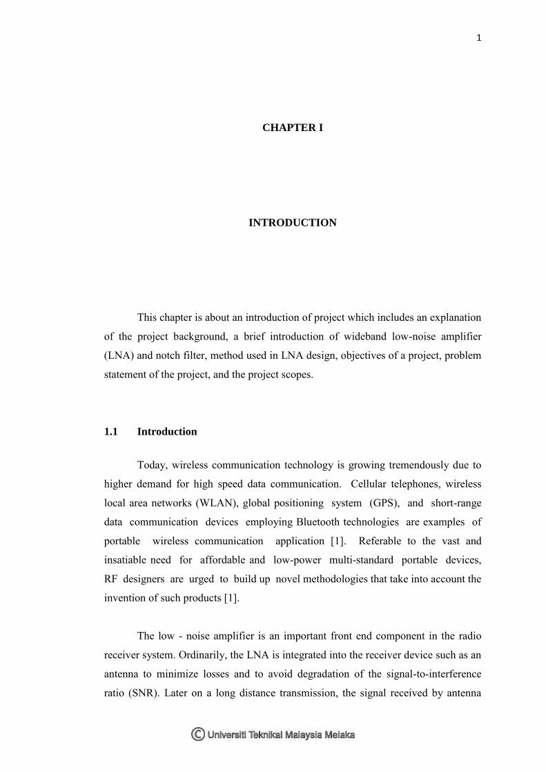
The basis block diagram of RF receiver structure is presented as Figure 1.1.
Before amplified by an LNA, the signal received by antenna is normally filtered by
RF filter first and then unite with a local-oscillator (LO) to metamorphose to the
base-band. After demodulated process, the signal is processed to an analog-to-digital
converter (ADC) which translates the analog signal into a digital signal. Then, the
digital signal is utilized in a digital signal processing unit (DSP). The primary step of
signal amplification is complete by the LNA. Therefore, the properties of LNA can
easily affect the overall noise and sensitivity parameter of the entire receiver [1].
Figure 1.1: Basis Block Diagram of RF Receiver.
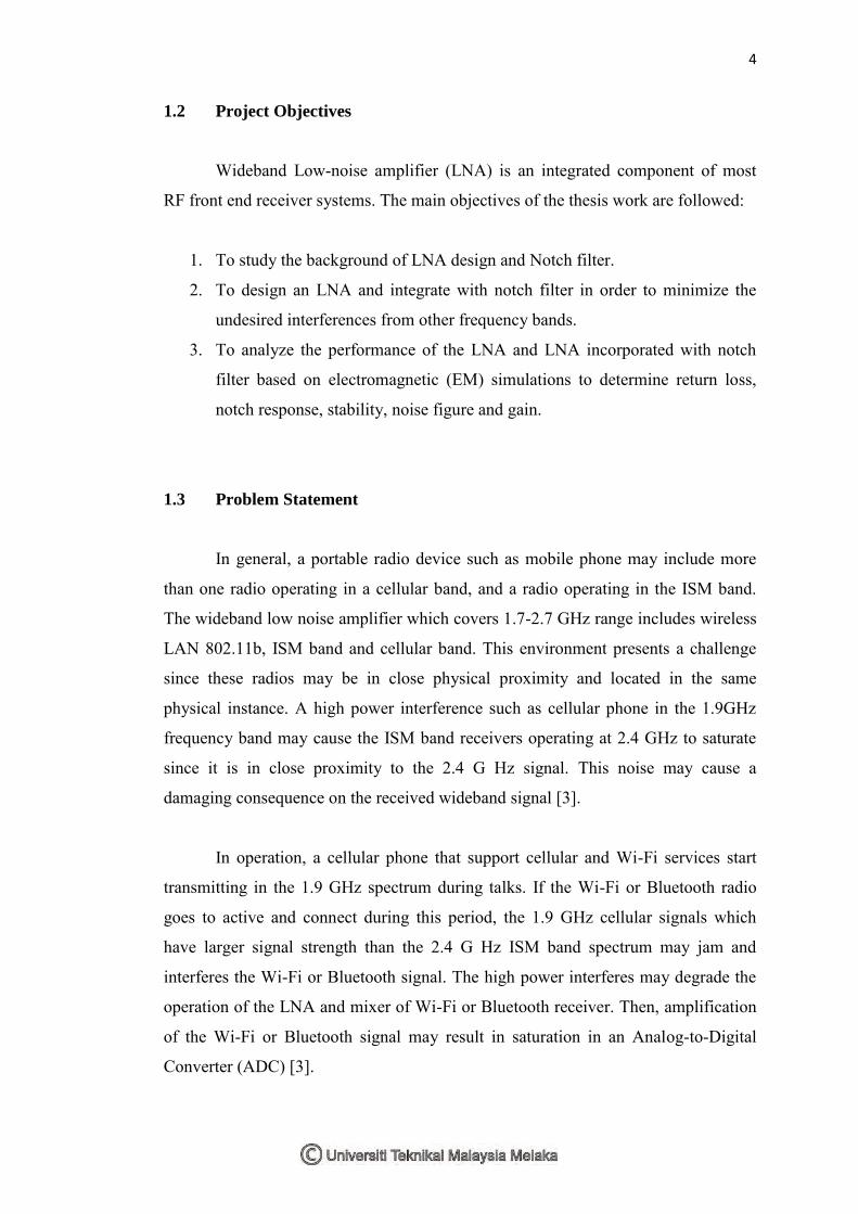
A notch filter greatly removes/ eliminates a specific frequency component of
the input signal spectrum while lets the amplitude of other frequencies relatively
unchanged and go. In general, a notch filter can be delineated as a band stop filter
with a very narrow stop band and two pass bands. Figure 1.2 depicts the
characteristic of a typical notch filter, the amplitude response is represented by
( ), notch frequency is and BW mean 3-dB rejection bandwidth. BW would
be zero, the pass band magnitude is unity (zero dB) and the attenuation at the notch
frequency is infinite if a notch filter is ideal [2].

3
Figure 1.2: The Characteristic of Notch Filter.
Generally, LNA and Notch filter are two different blocks in a recipient. This
project is attempting to integrate LNA and Notch filter in one block which is more
cost effective and have less complexity of the circuit and the size of the receiver will
go smaller as well. The integration of Low-Noise Amplifier and Notch Filter for
wireless communication application which covers the frequency range of 1.7 GHz –
2.7 GHz is designed in this project. The wideband LNA are designed using transistor
Avago Technologies’ ATF-54143 for the whole design process. As referred to the
data sheet at Appendix A, this type of transistor is built by GaAs Enhancement-mode
pHEMT in a Surface Mount Plastic Package. Avago Technologies’ ATF-54143 is a
high dynamic range, low noise, E-PHEMT housed in a 4-lead SC-70 (SOT-343)
surface mount plastic package. This transistor is optimized for 3V operation and
exhibit exceptional RF performance, power efficiency and product consistency in the
450 MHz to 6 GHz frequency range. The transistor can be used in many applications,
for example front end LNA for Cellular/PCS base stations, LNA for WLAN,
WLL/RLL and MMDS applications.
4
1.2 Project Objectives
Wideband Low-noise amplifier (LNA) is an integrated component of most
RF front end receiver systems. The main objectives of the thesis work are followed:
1. To study the background of LNA design and Notch filter.
2. To design an LNA and integrate with notch filter in order to minimize the
undesired interferences from other frequency bands.
3. To analyze the performance of the LNA and LNA incorporated with notch
filter based on electromagnetic (EM) simulations to determine return loss,
notch response, stability, noise figure and gain.
1.3 Problem Statement
In general, a portable radio device such as mobile phone may include more
than one radio operating in a cellular band, and a radio operating in the ISM band.
The wideband low noise amplifier which covers 1.7-2.7 GHz range includes wireless
LAN 802.11b, ISM band and cellular band. This environment presents a challenge
since these radios may be in close physical proximity and located in the same
physical instance. A high power interference such as cellular phone in the 1.9GHz
frequency band may cause the ISM band receivers operating at 2.4 GHz to saturate
since it is in close proximity to the 2.4 G Hz signal. This noise may cause a
damaging consequence on the received wideband signal [3].
In operation, a cellular phone that support cellular and Wi-Fi services start
transmitting in the 1.9 GHz spectrum during talks. If the Wi-Fi or Bluetooth radio
goes to active and connect during this period, the 1.9 GHz cellular signals which
have larger signal strength than the 2.4 G Hz ISM band spectrum may jam and
interferes the Wi-Fi or Bluetooth signal. The high power interferes may degrade the
operation of the LNA and mixer of Wi-Fi or Bluetooth receiver. Then, amplification
of the Wi-Fi or Bluetooth signal may result in saturation in an Analog-to-Digital
Converter (ADC) [3].
5
Some existing solutions may incorporate an on-board notch filter in the ISM
band radio. This notch filter may be located between a low noise amplifier (LNA)
and the mixer in the RF portion of the ISM band radio. This is to minimize the
undesired interferences from other frequency bands [3].
1.4 Scope of Work
For this project, the scope is to design Integrated Low-Noise Amplifier and
Notch Filter for wireless communication application which covers the frequency
range of 1.7 GHz – 2.7 GHz. It can be split into five parts which are:
i. To study on how to design an integrated Low-Noise Amplifier and Notch
Filter which covers the frequency range of 1.7 GHz – 2.7 GHz and can
support wireless communication application.
ii. In design working process consists of three main parts which is
simulation, testing, analysis and optimization.
iii. The S-parameter that is involved in the design such as noise figure, gain,
return loss and notch response is analyzed.
iv. The design and simulation of integrated low noise amplifier and notch
filter will be done by using Advanced Design System (ADS).

6
1.5 Chapter Review
Chapter 1 is about an introduction of project which includes an explanation of
the project background, a brief introduction of the wideband low noise amplifier
(LNA) and notch filter, objectives of a project, problem statement, and the project
scopes.
Chapter 2 is about the background study define in details for integrated low
noise amplifier and notch filter. The literature review of the low noise amplifier,
especially on the parameters and the design techniques used in the design procedure
to also define in detail.
Chapter 3 contains research methodologies which include the step to design
the integrated low noise amplifier and notch filter. This chapter also includes detailed
explanations of a low noise amplifier and notch filter design technique and
calculation that involved.
Chapter 4 is discussing about the results and analysis the simulation of
integrated low noise amplifier and notch filter from stability consideration until the
implementation of the LNA and notch filter.
Chapter 5 reveals the main summarization and the conclusion of this project
and finally the future works suggestions on this project.

7
CHAPTER II
LITERATURE REVIEW
This chapter defines about the background study define in details for
integrated of a low noise amplifier and notch filter. The literature review of the low
noise amplifier, especially on the parameters and the design techniques used in the
design procedure to also set in detail.
2.1 Frequency Bands of 1.7 to 2.7 GHz
There are several frequency bands including in the 1.7 to 2.7 GHz frequency
range, which is ISM band, GSM cellular bands and others.
2.1.1 ISM Band
The ISM (Industrial, Scientific and Medical) bands are open frequency bands,
varying by region, that allow for operation without a license and free uses. The uses
of these bands become very popular for short-range communication and low power
communication electronics systems. The 2.4 GHz band is one of the ISM band, it
utilized for worldwide operation and often hosts for standardized and proprietary
protocols such as wireless LAN 802.11b, Bluetooth, ZigBee, Z-Wave and others [4].