uidebook-...dc amplifier-dc voltage amplifier-dc galvanometer ... push-pull transmitter -type rf...
TRANSCRIPT

Q_T1%%)TAB BOOKS / No. 796 64.95
FET
UIDEBOOK-
100 lytartied einatiti trait. tPet ittitituixo4 oudia abigilotg/tyate
RF/AF riettatizol, 44.uite.11.4t . cIttfiren, eadeatvo, Gookast awl /4k -wave
4Preioena, awl a Vect-fakvexecl ticutiretten.... aff o-cattie, we41eitona.e MOSFET!

MOSFET CIRCUITS
GUIDEBOOK-witk 100 Toted Pak&

Other TAB books by Rufus P. Turner
Book No. 63 Transistor Circuits
Book No. 69 Electronic Hobbyist's Handbook
Book No. 75 Transistors-Theory & Practice
Book No. 537 125 One -Transistor Projects

MOSFET CIRCUITS
GUIDEBOOK-with, 100 Tata Neet,
Bg Rutta P Twuitex
TAB BOOKSBlue Ridge Summit, Pa. 17214

FIRST EDITION
FIRST PRINTING-OCTOBER 1975
Copyright c 1975 by TAB BOOKS
Printed in the United States of America
Reproduction of the content in any manner. without express permission of the publisher. is prohibited. No liability is assumed with respect to the use
of the information herein.
Hardbound Edition: International Standard Book No. 0-8306-5796-7
Paperbound Edition: International Standard Book No. 0-8306-4796-1
Library of Congress Card Number: 75-27483

Contents
Preface 9
Chapter 1Meet The MOSFETDescription of mosFET-Operating Modes-Advantages and Dis-advantages-Gate-Protected MOSFET-MOSFETS Used in ThisBook-Hints and Precautions
Chapter 2AF AmplifiersSingle -Stage RC -Coupled Amplifier-High-Gain Single -StageAmplifier-Two-Stage High -Gain Amplifier-DegenerativeAmplifier-Source Follower-MosFET-Bipolar Amplifier withAGC-MOSFET Input For IC Amplifier-Dual-Input AFMixer-Dual-MosFEr Phase Inverter-Paraphase Amplifier-Gated-On Amplifier-Gated-Off Amplifier-LC-Tuned Low -PassAmplifier-RC-Tuned Low -Pass Amplifier-LC-Tuned High-Pass Amplifier-RC-Tuned High -Pass Amplifier-LC-TunedPeak Amplifier-RC-Tuned Peak Amplifier-LC-Tuned NotchAmplifier-RC-Tuned Notch Amplifier-Headphone Amplifier-Peaked-Response Headphone Amplifier
Chapter 3DC, RF, And IF AmplifiersDC Amplifier-DC Voltage Amplifier-DC GalvanometerAmplifier-DC Source Follower-General-Purpose RFAmplifier-Single-Ended Transmitter -Type RF Amplifier-Push-Pull Transmitter -Type RF Amplifier -100 MHz RFAmplifier-Single-Tuned IF Amplifier-Double-Tuned IFAmplifier-Regenerative IF Amplifier-Video ( Wideband )Amplifier
11
18
60

Chapter 4 Control Circuits and Devices
Zero -Current DC Relay-AC RF Relay-Sensitive AF Relay- LC-Tuned AF Relay-RC-Tuned AF Relay-Coincidence
Relay-Touch-Plate Relay-Capacitance Relay-Sound Switch-Interval Timer-Continuously Variable Phase Shifter-
Step-Type Phase Shifter-Sensitive Carrier -Failure Alarm- Logic AND Circuit-Logic OR Circuit-DC Signal Inverter-DC
Impedance Converter-Dual-Polarity Output Adapter
Chapter 5 Oscillators
Tickler -Type Audio Oscillator-Hartley Audio Oscillator- Colpitts Audio Oscillator-Franklin Audio Oscillator-Phase-
Shift Audio Oscillator-Wien-Bridge Audio Oscillator-Villard Audio Oscillator-Multivibrator-Sun-Powered Audio
Oscillator-Self-Excited RF Tickler -Coil Oscillator-Self- Excited RF Hartley Oscillator-Self-Excited RF Colpitts
Oscillator-Standard Crystal Oscillator-Pierce Crystal Oscillator-Sun-Powered RF Oscillator-Self-Excited IF
Oscillator-Crystal-Controlled IF Oscillators
Chapter 6 Test Instruments
Single-MosFET Electronic DC Voltmeter-Balanced Electronic DC Voltmeter-Center-Zero Electronic DC Voltmeter-Self-
Excited Frequency Standard-AF-RF Signal Tracer-Tuned RF-IF Signal Tracer-AF Signal -Tracer Adapter For AC
Voltmeter-Active Probe-Wide-Range LC Checker-AC Null Detector-Sensitive Light Meter-Sine- to Square -Wave Con-
verter-AM Monitor-CW Monitor
Chapter 7 Miscellaneous Circuits
Constant -Current Adapter-Charge Detector (Electroscope)- Flip-Flop-Supersonic Pickup-Balanced Modulator-Simple
Light -Beam Receiver-Sensitive Light -Beam Receiver- Regenerative Broadcast Receiver-All-Wave Regenerative Receiver-RF Mixer-Tuning Meter-Heterodyne Eliminator- Flea-Power "QRP" Transmitter-Frequency Doubler-
Reactance Modulator
81
116
145
170
Index 194

Preface
The metal -oxide -semiconductor field-effect transistor,abbreviated MOSFET, is easily applied to electronic circuits ofvarious types. In several respects, the MOSFET resembles thevacuum tube more closely than do the bipolar transistor andthe conventional field-effect transistor, and this featureenables some circuits to be more easily transistorized.
This book offers a collection of tested MOSFET circuits,many of them employing only one transistor. These arelargely old vacuum -tube favorites of experimenters andhobbyists. adapted to the MOSFET. Very little space is devotedto MOSFET theory: the reader is assumed to know already howa regular field-effect transistor works and to need only a brieffill-in on special features of the MOSFET.
For convenience, the circuits are grouped intoconventional categories: amplifiers, oscillators, instruments,and so on. Each chapter is completely self-contained, so thatthe reader is not forced to refer to prior sections. The selectedcircuits are practical, and they offer an excellent opportunityto get acquainted with the MOSFET.
General instructions for handling, installing, and usingMOSFETS of the type shown in this book are given in Chapter 1
under the heading Hints and Precautions, and the readershould study these carefully before starting his experiments.
Rufus P. Turner

Chapter 1
Meet The MOSFET
This chapter describes the principal features of the MOSFET.Since the reader is assumed to know how a conventionalfield-effect transistor works and is structured, no space isdevoted here to basic theory. Only those MOSFET features arediscussed that the reader must be familiar with in order to usethis device safely and effectively. For additional material,both theoretical and practical, the reader is referred to theconsiderable literature on field-effect devices.
The instructions for handling and using the MOSFET shouldbe read carefully by newcomers to MOSFET practice beforethey experiment with the device.
DESCRIPTION OF MOSFETThe MOSFET ( metal -oxide -semiconductor field-effect
transistor) is a special type of field-effect transistor in whichthe gate electrode is a small metal plate insulated from thesubstrate by a thin film of silicon dioxide. The gate leakagecurrent-as low as 10 picoamperes ( 10 -11 ampere) in somemodels-is much less than that in the junction FET and resultsin an input resistance comparable to that of the vacuum tube.To all practical intents and purposes, therefore, the MOSFET,like the vacuum tube, is essentiallya voltage -actuated device.
Figure 1-1 shows the basic structure of an N -channelMOSFET. Although this may not be the precise cross section of aparticular unit, it illustrates the main differences betweenMOSFETs and conventional junction FETs. In this sketch, thevarious regions are not to scale. In the P -type silicon wafer
11

SOURCE (S)
GATE (G)
N -CHANNEL
OXIDE r- METAL ELECTRODE
SUBTRATE (SUB)
Fig. 1-1. Basic MOSFET structure.
DRAIN (D)
(the substrate), the source (S) and drain (D) electrodes consist of small N -regions that are processed into the wafer.
When an external voltage is applied between the source and drain, current carriers flow through the "channel" between these two regions. The gate electrode (G), which
electrostatically controls these carriers, consists of a small metal film placed close to, but not touching, the wafer. The
thin oxide film provides the insulation needed to keep the metal gate out of contact with the wafer. The corresponding
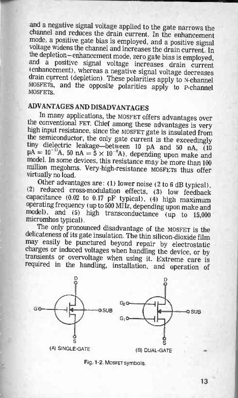
circuit symbol is shown in Fig. 1-2A. This particular kind of device is known as an N -channel MOSFET.
If the NS and Ps are interchanged in Fig. 1-1, we have instead a P -channel MOSFET; the circuit symbol will differ only
in reversal of the arrow. For the N -channel device, the external DC voltages are: drain positive, source negative. For the
P -channel device, the voltages are: drain negative, source positive.
Single -gate MOSFETS and dual -gate MOSFETS both are commercially available. Type 3N128, for example, is a
single -gate unit, and type 3N140 is a dual -gate unit. Figure 1-2B
shows the circuit symbol of a dual -gate MOSFET. Note, that there are two gates and one drain; thus, the dual -gate MOSFET
is comparable to a tube such as type 6AE7-GT, which has two control grids and one plate. The dual -gate device is
particularly useful in converter, mixer, push -push doubler, and AGO -controlled circuits.
OPERATING MODES There are three operating modes for MOSFETs: depletion
mode, enhancement mode, and depletion-enhancement mode. In the depletion mode, a negative gate bias is employed,
12
and a negative signal voltage applied to the gate narrows thechannel and reduces the drain current. In the enhancementmode, a positive gate bias is employed, and a positive signalvoltage widens the channel and increases the drain current. Inthe depletion-enhancement mode, zero gate bias is employed,and a positive signal voltage increases drain current(enhancement), whereas a negative signal voltage decreasesdrain current (depletion). These polarities apply to N -channelMOSFETS, and the opposite polarities apply to p -channelMOSFETS.
ADVANTAGES AND DISADVANTAGESIn many applications, the MOSFET offers advantages over
the conventional FET. Chief among these advantages is veryhigh input resistance, since the MOSFET gate is insulated fromthe semiconductor, the only gate current is the exceedinglytiny dielectric leakage-between 10 pA and 50 nA, (10pA = 10-"A, 50 nA = 5 x 10⁻⁸A), depending upon make andmodel. In some devices, this resistance may be more than 100million megohms. Very -high -resistance MOSFETS thus offervirtually no load.
Other advantages are: (1) lower noise (2 to 6 dB typical),(2) reduced cross -modulation effects, (3) low feedbackcapacitance (0.02 to 0.17 pF typical), (4) high maximumoperating frequency (up to 500 MHz, depending upon make andmodel), and (5) high transconductance (up to 15,000micromhos typical).
The only pronounced disadvantage of the MOSFET is thedelicateness of its gate insulation. The thin silicon -dioxide filmmay easily be punctured beyond repair by electrostaticcharges or induced voltages when handling the device, or bytransients or overvoltage when using it. Extreme care isrequired in the handling, installation, and operation of
SUB
S
(A) SINGLE -GATES
(B) DUAL -GATE
Fig. 1-2. MOSFET symbols.
SUB
13

62
G1 Fig. 1-3. Gate -protected MOSFET.
conventional MOSFETS. However, a special gate -protected MOSFET is commercially available (as a dual -gate model), and
this type can be handled with the ordinary care given to any transistor. This nearly foolproof MOSFET is described below. Some appraisers cite the input capacitance of the
mosFET-due to the equivalent capacitor formed by the metal gate, oxide insulation, and underlying semiconductor
wafer-as a disadvantage. However, this capacitance (typically 3 to 6.5 pF) is no great impediment to the designer
or user, as it is only slightly higher than the input capacitance of many tubes having the same transconductance, and is very
much smaller than the input capacitance of some tubes.
GATE -PROTECTED MOSFET Figure 1-3 shows the circuit symbol of the gate -protected
MOSFET. In this arrangement, each gate is internally connected through a pair of integrated back -to -
back -connected zener diodes (D, and D2 for gate 2, and D3 and D4 for gate 1) to the substrate and source. At low
voltages ( including normal gate bias and normal peak signal voltage), the reverse -connected diode in each pair is
essentially nonconducting; i.e., it offers extremely high resistance and does not interfere with MOSFET performance.
(For a given polarity of gate voltage, one diode in each leg is reverse biased and the other is forward biased; when the polarity reverses, the bias conditions are reversed.) The diode leakage current is of the order of 1 to 50 nA (1 nA = 10-9A),
depending upon MOSFET make and model and gate voltage. In classic fashion, when the gate voltage rises above a prescribed
safe level, the reverse -biased diodes undergo zener breakdown and conduct relatively heavily, providing a short-circuit path
around the gate and protecting the gate insulation. The integrated diodes do increase the gate leakage current
and the input capacitance of the gate -protected MOSFET
14
somewhat, but in many applications the protection againstMOSFET destruction is well worth this slight disadvantage.
MOSFET USED IN THIS BOOKIn the experimenter's interest, only gate -protected
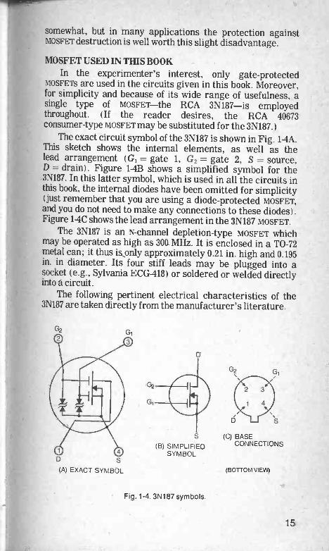
MOSFETS are used in the circuits given in this book. Moreover,for simplicity and because of its wide range of usefulness, asingle type of mosFET-the RCA 3N187-is employedthroughout. ( If the reader desires, the RCA 40673consumer -type MOSFET may be substituted for the 3N187.)
The exact circuit symbol of the 3N187 is shown in Fig. 1-4A.This sketch shows the internal elements, as well as thelead arrangement (G, = gate 1, G2 = gate 2, S = source,D = drain). Figure 1-4B shows a simplified symbol for the3N187. In this latter symbol, which is used in all the circuits inthis book, the internal diodes have been omitted for simplicity(just remember that you are using a diode -protected MOSFET,and you do not need to make any connections to these diodes).Figure 1-4C shows the lead arrangement in the 3N187 MOSFET.
The 3N187 is an N -channel depletion -type MOSFET whichmay be operated as high as 300 MHz. It is enclosed in a TO -72metal can; it thus isonly approximately 0.21 in. high and 0.195in. in diameter. Its four stiff leads may be plugged into asocket (e.g., Sylvania ECG -418) or soldered or welded directlyinto a circuit.
The following pertinent electrical characteristics of the3N187 are taken directly from the manufacturer's literature.
(A) EXACT SYMBOL
02
01
S
(B) SIMPLIFIEDSYMBOL
Fig. 1-4. 3N187 symbols.
(C) BASECONNECTIONS
(BOTTOM VIEW)
15

Drain -to -source volts (V0s) Gate -l -to -source volts ( Vms) Gate -2 -to -source volts ( VG2s)
Maximum drain current (
Device dissipation ( 25°C) Power gain (Go,) Noise figure (NF)
Forward transconductance (Gib) Gate leakage current ( Icss) Input capacitance (C,,,)
Reverse transfer capacitance (Cr,.,) Gate -l -to -source pinchoff voltage ( Vp01)
Gate -2 -to -source pinchoff voltage ( Vp02)
Output resistance (r°,,) =
( Vos)
ID = 10 mA, V
G2S = 4V,
-0.2V to +20V max +3V to -6V DC, ±6V peak AC
-6% to 30% of VDs DC
50 mA 330 mW
18 dB typ at 200 MHz 4.5 dB max at 200 MHz
7000 µmho min; 12,000 µmho typ 50 nA max 6 pF typ
0.03 pF max -2V typ -2V typ
280052
= 200 MHz
HINTS AND PRECAUTIONS For maximum protection of the MOSFET and best results
from its use, the following hints are offered:
1. Employ the exact values of components and voltages specified in the circuit diagrams. Adjust a circuit
( where this is needed) exactly as instructed in the text.
2. The reader is free to use his favorite method of construction: perforated board, open chassis, metal
box, printed circuit. Use the same techniques and precautions that would apply to any other
transistorized device. 3. All methods of transistor mounting are suitable for the
MOSFET. These include use of socket, soldering or welding directly into circuit ( use a suitable heatsink),
use of clips, use of mounting screws, use of terminal studs.
4. After completing a project, check all wiring carefully, and insert the MOSFET last.
5. Be sure the pigtail leads are straight before inserting the MOSFET into a socket, and insure that each lead is in the correct hole (see Fig. 1-4C). To drive the MOSFET
home, push firmly, but gently and straight down, on the top of the case.
6. Like other transistors, a gate -protected MOSFET such as the 3N187 is reasonably rugged mechanically and
need not be handled gingerly. Nevertheless, it should not be abused mechanically. Avoid rough handling,
dropping, hammering, and similar abuse. Do not
16

t.
stress the pigtail leads. Use care when removing aMOSFET from its socket.
7. The metal case of the 3N187 is "hot" ; that is, the caseis internally connected to the substrate and source.Therefore, do not allow the case to come into contactwith leads, chassis, or other components.
8. In all MOSFET circuits, use the shortest and most directleads that are practicable. This will minimize straypickup, undesired coupling, and undesired feedback.
9. When using only one gate of a dual -gate MOSFET, do notallow the other gate to float, especially if a lead isconnected to it. Either ground the unused gate,connect it to the source, or connect a 10001/ resistorbetween this gate and ground. A floating gate is highlysusceptible to stray pickup and body capacitance.
10. In all RF circuits and high -gain AF circuits, shield allsusceptible parts of the circuit just as you would in atube circuit. When long leads are unavoidable, leaddress is important.
11. Do not subject the mosFET to excessive currents orvoltages. (Refer to the electrical characteristics of the3N187.)
12. Never allow the combined gate voltage (Dc bias pluspeak AC signal voltage) . to exceed the maximumgate -voltage rating of the MOSFET.
13. Avoid exposing the MOSFET to strong magnetic fields.14. Protect the MOSFET from excessive heat.15. In some of the circuit diagrams, a dashed line runs to
the ground symbol. This means that the connection tochassis or to earth, as the case may be, is optional anddepends upon how the circuit will be used by thereader. When, instead, a solid line runs to the groundsymbol, the connection must be made.
17

Chapter 2
AF Amplifiers
This chapter presents 22 audio -frequency circuits, including single -stage amplifiers, 2 -stage amplifiers, tuned amplifiers,
and phase inverters. One circuit shows a common way of using a MOSFET with a bipolar transistor to obtain the best features
of each; another circuit shows how a MOSFET may be operated ahead of a conventional integrated circuit to provide high input
impedance for the latter. Some newcomers to MOSFET applications will choose these audio applications as a means of
getting acquainted with the device. In each of the circuits, unless otherwise indicated on the circuit diagram or in the text, capacitances are in picofarads
and resistances in ohms. Resistors are 1/2W, and electrolytic capacitors have a DC working -voltage rating of 25V. The similarity of the components to those used in equivalent tube
circuits will be readily apparent to the experienced reader. For simplicity, batteries are shown for DC supply;
however, a well filtered power supply may be used instead. Before undertaking the wiring and operation of any
circuit, read carefully the hints and precautions given in Chapter 1.
SINGLE -STAGE RC -COUPLED AMPLIFIER Figure 2-1 shows the circuit of a single -stage amplifier employing a 3N187 MOSFET in the common -source circuit. This
circuit is equivalent to the grounded -cathode tube circuit and the common -emitter bipolar -transistor circuit.
The MOSFET is biased to operate in its linear region by means of a combination of (1) gate -1 negative bias developed
18

C r01µ
F
AF
INP
UT
(0.1
V R
MS
MA
XA
TG
1)O
0 5M
Ri <
GA
IN
// C
HA
SS
IS
R
Par
ts
0.5M
R2
470K
R3
1.5M
R4
270
R5
1800
C1
0.1
I.L.F
C2
50 i.
LF
C3
0.1
p..F
B6V
, 1.6
mA
S S
PS
TO
3N
187
R3
R5
Z 1
800
1.5M
470K
R4
270
C2T
50µF
C3
IF
0.1µ
F
ON
-OF
F
B6V
T-
1.6
mA
Fig
. 2-1
. Sin
gle
-sta
ge R
C -
coup
led
ampl
ifier
.
AF
OU
TP
UT
(1V
RM
S M
AX
)
0

by the flow of drain current through source resistor R4, and (2)
gate -2 positive bias developed by voltage divider R2-R3. In this divider, resistance R3 may need to be adjusted with an
it 3N187 for linear operation. The input resistance of the amplifier is approximately
'2M, the resistance of the gain -control potentiometer RI. The high gate resistance of the MOSFET enables the use of a high -resistance potentiometer here.
Current drain from the 6V supply B is approximately 1.6
mA. Open -circuit voltage gain of the single stage is 10. The maximum input -signal voltage before output -peak clipping is
0.1V RMS at gate 1 (higher amplitude signals are reduced to this maximum by appropriate settings of potentiometer R 1)
. The correspondingmaximumoutput is 1V RMS. Response of the
circuit is flat within ±2 dB of its 1000 Hz response from 50 Hz to 25 kHz. If the DC supply is increased to 12V (2.6 mA )
,
the open -circuit voltage gain increases to 15 ( maximum input -signal voltage equals 0.2V RMS at gate 1; corresponding
maximum output -signal voltage before peak clipping equals 3V RMS)
.
HIGH -GAIN SINGLE -STAGE AMPLIFIER Operating with a higher DC voltage and different circuit
constants, the single -stage RC -coupled amplifier shown in Fig. 2-2 provides almost four times the voltage gain afforded by the
similar amplifier described in the preceding section. There are numerous applications in which high single -stage gain is
desired: preamplifiers, AC voltmeter amplifiers, signal boosters for electronic relays and other control devices,
electronic games, oscilloscope amplifiers and preamplifiers, etc.
The amplifier is biased into its linear region by a negative voltage applied to gate 1 and a positive voltage applied to gate
2. The negative bias is developed by the flow of drain current through source resistor R4; the positive bias is developed by
the voltage divider R2-R3, operated from the DC supply (battery B). In an individual setup, resistor R3 in this divider
may need some adjustment for linear operation of the amplifier.
The input resistance of the amplifier is approximately 1/2M, the full resistance of the gain -control potentiometer R
Higher input resistance may be obtained, at some chance of
stray pickup, by increasing the resistance of this potentiometer. The high gate resistance of the MOSFET enables
the use of a high -resistance potentiometer in this position.
20

AF
INP
UT
(50
mV
RM
S M
AX
AT
G1)
O
3N18
7
5M
GA
INR
3
/-1-
7C
HA
SS
IS
Par
ts
R1
0.5M
R2
470K
R3
3.3M
R4
3.3K
R5
15K
CI
0.1
/IFC
2 50
µF03
0.1µ
FB
12V
, 0.5
mA
S S
PS
TO
3N18
7
R5
3.3M
R2
470K
R4
3.3K
C2
50µF
Fig
. 2-2
. Hig
h -g
ain
sing
le -
stag
e am
plifi
er.
15K
C3
0.1I
f µF
SO
N-O
FF
B--
-12
V 0.5
mA
I
AF
OU
TP
UT
(1.8
V R
MS
MA
X)
0

Current drain from the 12V supply B is approximately 0.5
mA. Open -circuit voltage gain of the single stage is 36. The maximum input -signal voltage before output peak clipping is
0.05V RMS at gate 1 ( higher amplitude signals are reduced to this maximum by appropriate settings of potentiometer R ,)
.
The corresponding maximum output is 1.8V RMS. Response of the circuit is flat within ±2 dB of its 1000 Hz response from 100
Hz to 50 kHz, and is -5 dB at 20 Hz.
TWO -STAGE HIGH -GAIN AMPLIFIER Figure 2-3 shows the circuit of an amplifier employing two
3N187 MOSFETS in cascade. The open -circuit voltage gain of
this amplifier is 1200. The stages are individually biased, with gate 1 of each MOSFET receiving a negative voltage, and gate 2 of each MOSFET a positive voltage. In the first stage, gate 1 of MOSFET
Q, receives the voltage drop developed across source resistor R4 by the flow of drain current, and gate 2 receives the voltage
developed by voltage divider R2-R3. In the second stage, gate 1 of MOSFET Q2 receives the voltage drop developed across
source resistor R10 by the flow of drain current, and gate 2
receives the voltage developed by voltage divider R8- Rg. With individual MOSFETS, voltage -divider resistors R3 and R9 may
require some adjustment for best linearity of the amplifier. The input resistance of the amplifier is approximately 1M,
determined by gate -to -ground resistor R1. A higher resistance may be used for RI, if desired, at some risk of stray pickup. The high gate resistance of the MOSFET Q, permits use of a high
resistance for HI. Current drain from the 12V supply B is approximately 1
mA. The maximum input signal voltage before output peak clipping is 1.5 mV RMS. The corresponding maximum output
signal voltage is 1.8V RMS. Response of the circuit is reasonably flat from 100 Hz to 20
kHz. The response is approximately -2 dB down at frequencies lower than 100 Hz and higher than 20 kHz. The
frequency response may be altered by suitably changing the capacitance of C1, C3, and C5.
Stable operation is enhanced by the decoupling filter consisting of resistor R, and capacitor C4. This coupler should
not be omitted from the circuit.
DEGENERATIVE AMPLIFIER The benefits of negative feedback in reducing distortion
and generally improving amplifier operation are obtained in the single -stage amplifier shown in Fig. 2-4 by employing an
22 1

Par
tsR
1115
KR
11M
C1
0.1
µFR
247
0KC
2 50
µFR
33.
3MC
30.
1 p.
FR
43.
3KC
410
µFR
515
KC
5 50
µFR
81K
C8
0.1µ
FR
70.
5MB
12V
, 1 m
AR
847
0KS
SP
ST
3N18
7
R9
3.3M
Qi
3N18
7R
io 3
.3K
423N
187
C1
-I(
0 1
µF
0A
F IN
PU
T(1
.5 m
V R
MS
Ri
MA
X)
1M
Qt
3
3.3M
R, 4
70K
R5
15K
0.1
µF
0.5M
R7
GA
IN
R4
3.3K
+
C,2
^ 50
µF
R6
10µF
1K
R11
15K
3N18
7
02
C5
0 1µ
F
R8
Rio
3.3K
"f"
C5
50 µ
F
0
AF
OU
TP
UT
(1 8
V R
MS
MA
X)
S 0
\ON
-OF
F
if12
VB
-1 m
A
/C
HA
SS
IS
Fig
. 2-3
. Tw
o -s
tage
hig
h -g
ain
ampl
ifier
.

1\3
Par
ts
R1
0.5M
C1
0.1
µFR
247
0KC
20.
1 /IF
0.1µ
FR
33.
3MB
12V
, 2.2
mA
R4
330
SS
PS
T3N
187
R5
15K
03N
187
0
01,F
0 5M
GA
IN
AF
INP
UT
(0 6
V R
MS
MA
X A
T G
1)
// C
HA
SS
IS
/R2
470K
R4
R3
R5
15K
3.3M
330
Fig
. 2-4
. Deg
ener
ativ
e am
plifi
er.
ON
- O
FF
B12
V
I2 2
mA
AF
OU
TP
UT
(22V
RM
S M
AX
)
0

unbypassed source resistor R4. The price for the improvedoperation is, of course, loss of gain. Thus, the voltage gain ofthis circuit, compared with that of its counterpart shown inFig. 2-1, is approximately 3.7.
The amplifier is biased into its linear region by a negativevoltage applied to gate 1 of MOSFET Q, and a positive voltageapplied to gate 2. The negative bias is developed as the voltagedrop across source resistor R4 ( produced by the flow of draincurrent through this resistor). The positive voltage isdeveloped by voltage divider R2-R3. With an individualMOSFET, resistor R3 in this divider may need some adjustmentfor best linearity of amplifier operation.
The input resistance of the amplifier is approximately1/2M, determined principally by the resistance of the gain-
control potentiometer RI. The high gate resistance of theMOSFET permits use of this high resistance at RI. If desired, ahigher R, resistance may be employed, at some risk of straypickup.
Current drain from the 12V supply is approximately 2.2mA. The maximum input -signal voltage before output peakclipping is 0.6V RMS at gate 1 (higher amplitude signals arereduced to this maximum by appropriate settings ofpotentiometer R,). The corresponding maximum output signalvoltage is 2.2V RMS.
SOURCE FOLLOWERFigure 2-5 shows the circuit of a simple source follower.
This circuit is equivalent to the vacuum -tube cathode followerand the bipolar -transistor emitter follower. Like the latter twocircuits, the source follower is a degenerative type employingnegative feedback to cancel stage -introduced distortion. Thecircuit is characterized by high input impedance and lowoutput impedance. As such, it has many well knownapplications in electronics, especially that of impedancetransformer with power gain. The source follower, like thecathode follower and emitter follower, is noted also for its widefrequency response and low distortion.
In this circuit, gate 1 and gate 2 are connected togetherand receive negative DC bias from the voltage drop producedby the flow of drain current through source resistor R2. Thehigh bypass capacitance C2 places the drain effectively atground potential. The input resistance of the stage isapproximately 1M and is largely determined by the fullresistance of gain -control potentiometer R,. For higher inputresistance, when this is desired, the resistance of R, may beincreased, at some risk of stray pickup. The approximate
25

IN)C
)
AF
INP
UT
(0.7
V R
MS
MA
XA
T G
1)
// C
HA
SS
IS
R1M G
AIN
3N18
7 Fig
. 2-5
. Sou
rce
follo
wer
.
C2
50µF
Par
ts
R1
1M
R2
500
Ci
0.1
/IFC
2 50
µFC
/3(S
EE
TE
XT
)B
7.5V
, 2 m
AS
SP
ST
Q.
3N18
7
G3
(SE
E T
EX
T)
BI 7.5V I-
1
- 2
mA
\ON
-OF
FA
F O
UT
PU
T
(0.3
6V R
MS
MA
X)

effective output impedance of the stage is 2771/ But this willdiffer somewhat with individual MOSFETS, since trans -conductance is a term in the impedance formula andvaries with MOSFE'M of the same type. The reader can vary R2for a desired value of output impedance. The outputimpedance is given by
ross R2R° - ( Yfsr, + 1) + (Eq. 2-1)
where
R, = output impedance ( ohms)R2 = source resistor value (ohms)r, = MOSFET output resistance ( ohms). ( See manufacturer'sliterature, but figure approximately 2800f/ for the 3N187.)
Yis transconductance of the MOSFET ( mhos) (Seemanufacturer's literature.)
Voltage gain of the stage is approximately 0.51. Themaximum input signal voltage before output peak clipping is0.7V RMS at the gates of the MOSFET (higher amplitude signalsare reduced to this maximum by appropriate settings ofpotentiometer R1). The corresponding maximum output signalvoltage is 0.36V RMS. You may obtain higher output voltage byincreasing resistance R2, and vice versa, but this will also affectthe value of output impedance ( see Eq. 2-1). The equation forvoltage gain of the source follower is
Y1 R2
GV - 1 + Yfs R2 (Eq. 2-2)
where Y fs and R2 have the same meanings as in Eq. 2-1.Response of the stage is reasonably flat from 100 Hz to 100 kHzand is approximately 2 dB down at 20 Hz. Current drain fromthe 7.5V supply is approximately 2 mA.
Output capacitor C3 will be required when this sourcefollower drives a stage or device to which direct coupling willbe undesirable. Its capacitance will be governed by theresistance or inductance that will be encountered in the drivendevice and the extent to which the LC or RC combinationalters the frequency response of the source follower.
MOSFET-BIPOLAR AMPLIFIER WITH AGCFigure 2-6 shows the circuit of a 2 -stage amplifier
employing a 3N187 MOSFET in the input stage and a 2N2712silicon bipolar transistor in the output stage. The stage
27

coP
arts
0.5M
C1
0.05
µFR
2 47
0KC
2 50
µFR
32.
2MC
30.
5µF
R4
15K
C4
50µF
R5
3.3K
C5
0.5µ
FR
6 47
KC
6 0.
5µF
0.05
µF
AF
INP
UT
(10
mV
RM
SM
AX
AT
G1)
O
177
CH
AS
SIS
0.5M
GA
IN
R3 R
47K
0.5
'IF
15K
RI1K
C50
µF
I\O
N-O
FF
B
+9N
/
1.5
mA
R12 inn
2.2M
Fig
. 2-6
. MO
SF
ET
- b
ipol
ar a
mpl
ifier
with
AG
C.
C5
0.5µ
F
1R
io 5
60K
D
R2
1KB
9V,1
.5 m
AR
94.
7MD
s1N
34A
R9
15K
S1
SP
ST
R10
560
KS
2S
PS
TR
11 1
5KG
I3N
187
R12
2.2
M02
2N27
12
S2,
0
ON
CA
TH
1N34
A
1R
i 115
K
AG
C AF
OU
TP
UT
(1.2
V R
MS
MA
X)

configuration is similar: common -source MOSFET andcommon -emitter bipolar transistor. This arrangement affordsthe high input impedance of the MOSFET and the high voltagegain of the bipolar transistor. An added advantage is overallautomatic gain control.
In the first stage, negative gate -1 bias for the MOSFET isprovided by the voltage drop resulting from the flow of draincurrent through source resistor R5, and positive gate -2 bias issupplied by voltage divider R2 -R3 (for an individual MOSFET,
resistor R3 in this divider may require some adjustment forlinear operation of the amplifier). In the second stage, the basebias of the 2N2712 transistor is the combination of the voltagedrop resulting from the flow of collector current throughemitter resistor R, and the output of voltage divider Rs R8.
The input impedance of the amplifier is approximately1/2M, determined principally by the full resistance ofgain -control potentiometer R,. A higher resistance ( e.g., 1M)may be used, if desired. The high gate resistance of theMOSFET permits use of a high -resistance gain control in what isessentially a transistorized amplifier.
Current drain from the 9V supply is approximately 1.5 mA.The overall voltage gain ( into open circuit orvery -high -resistance load) is 120. The maximum input signalvoltage before output peak clipping is 10 mV RMS at gate 1 ofMOSFET Q, (higher amplitude signals are reduced to thismaximum by appropriate settings of potentiometer R1). Thecorresponding maximum output signal voltage is 1.2V RMS.
These figures are obtained with AGC switch S2 open ( i.e., AGCoff). When S2 is closed, the rectifier circuit D- R10- R is cutinto the circuit, rectifies a portion of the output signal, andsends the resulting DC through filter R12 -C6 to gate 2 of theMOSFET Q,. The germanium diode D is poled for negative DC
output, and this negative voltage at gate 2 of Q, reduces thegain proportionately in the input stage.
MOSFET INPUT FOR IC AMPLIFIERWhile integrated circuits having MOSFET transistors
processed into them are obtainable, a great manyconventional is amplifiers with conventional bipolar transistorinput are in the hands of hobbyists and experimenters. Figure2-7 shows one way of providing high -impedance MOSFET inputfor such an integrated circuit. The ic here is an RCA 3020. Thisintegrated circuit is a complete audio amplifier having threeintermediate stages and a push-pull class B output stagedelivering 1/4W of AF power. The input resistance provided bythe MOSFET Q is governed largely by the resistance of
29

O
Ci
r01
µ F
AF
INP
UT
(0.7
V R
MS
MA
X)
R1
470K
TO 1M
3N18
7
R2
G2 /T
/)iR
4R
4 2 C6
6
IC
CA
3020
1011
12p
UN
US
ED
500
/ CH
AS
SIS
C4
R3
5K
1µF
03T
O01
µF
1 µF
8 97
PR
I: 10
0 O
HM
S C
TS
EC
: 3.2
OH
MS
TS
PK
R
R5
R4
0.62
R5
510K
510K
C1
0.1
pf.
C2
100µ
F
ON
-OF
FC
30.
01 µ
F IGN
AL:
14
mA
B -
6V
ZE
RO
ST
MA
X S
IGN
AL:
87
mA
Fig
. 2-7
. MO
SF
ET
inpu
t for
is a
mpl
ifier
.
rPar
tsR
147
0K to
1M
R2
500
C4
1A
35K
C5
1C
g1
µFB
6V
IC C
A30
20S
SP
ST
Q 3
N18
7

gate -to -ground resistor RI and can be any value between 470Kand 1M. The higher values will make the setup moresusceptible to stray pickup. The input stage is a sourcefollower.
In the outboard input stage, the two gate electrodes of theMOSFET are connected together and receive their negative biasfrom the voltage drop developed across source resistor R2. Theoutput of the is is coupled to a 3.2f/ speaker through aminiature, transistor -type transformer T having a 100f/,centertapped primary winding and 3.2fl secondary.
Since the ic contains a class B stage, the direct -currentdrain will be different under quiescent and driven conditions:The zero -signal current drain from the 6V source thus is 14mA, and the maximum -signal drain is 87 mA, approximately.Higher audio power may be obtained by appropriatelyincreasing the battery voltage; however, for powers in thevicinity of 1/2W, a heatsink must be used with the ic. For 1/4Woutput with minimum distortion, the maximum input signalvoltage is 0.7V RMS. Since the gain control R3 is at the input ofthe second stage of this circuit, the signal must be limited tothis maximum at the amplifier input.
DUAL -INPUT AF MIXEROne of the merits of the dual -gate MOSFET is its low
cross -modulation characteristic. This feature allows thedevice to be employed effectively in converters and mixers.Figure 2-8 shows the circuit of a dual -input audio -frequencymixer employing a single 3N187 MOSFET.
Here, AF input 1 is applied to gate 1 of the MOSFET through1/2M gain -control potentiometer Ri, and AF input 2 is applied togate 2 through 1/2M gain -control potentiometer R2. Gate 1receives negative bias resulting from the voltage dropdeveloped by the current through source resistor R5 gate 2receives positive bias produced by the output of voltagedivider R3 -R4. The common output signal is developed acrossdrain resistor R6 and is coupled to the output through capacitorC5. The resistance at each signal input is approximately 0.5M,determined largely by the resistance of potentiometer R, orpotentiometer R2. Higher input resistance may be obtained bysubstituting higher resistance potentiometers, at some risk ofstray pickup.
Current drain from the 6V source is approximately 3 mA.The open -circuit voltage gain for each half of the circuit is 10.The maximum input signal voltage before output peak clippingis 0.1V RMS at gate 1 or gate 2 (higher amplitude signals arereduced to this maximum by appropriate settings of
31

O0.
1 µF
AF
INP
UT
1
C2
0.1
I( µFR
2
0 5M
I
Cs
3N18
70
0.5M
GA
IN
GA
IN
AF IN
PU
T 2
R3
1500
// C
HA
SS
IS
T10
0
R4
Par
ts
R1
0.5M
C2
0.1
/IFR
20.
5MC
310
0µF
R3
1500
C4
50µF
R4
4700
Cs
0.1
µFR
6
R5
330
B6V
, 3 m
A
R6
1800
SS
PS
T
C1
0.1
µFQ
3N18
7
4700
R5
li:I3
30C
450
µF
Fig
. 2-8
. Dua
l -in
put A
F m
ixer
.
0.1
µF
1800
Sk
ON
-O
FF
LB
=.6
V 3
mA
AF
OU
TP
UT

gain -control potentiometers R1 and R2). The correspondingmaximum output signal voltage is 1V RMS.
Like its tube and transistor counterparts, this mixer willoperate from a combination of devices. Examples are: twomicrophones, two players, one microphone and one player,and so on.
DUAL-MOSFET PHASE INVERTERFigure 2-9 shows the circuit of a conventional dual -device
phase inverter adapted for mosFETs. This circuit is applicableto many experimental uses, as well as to its usual applicationof driving a push-pull amplifier. In this arrangement, the AFinput signal is first amplified by MOSFET Q1, which, because ofthe common -source circuit, provides a 180° phase shift at thejunction of R9 and C4. This output signal is sampled bypotentiometer R11, which returns a fraction of the signal to theinput of MOSFET Q2, which then amplifies this fraction andshifts its phase by 180°. The output of Q2 is delivered to thephase -2 output terminal. In this way, the two output signals areof opposed phase, with respect to the common output terminal.Balance -control potentiometer RI, is adjusted for equalamplitude of the phase -1 and phase -2 output signals.
In this circuit, gate 1 of MOSFET Q, receives negative biasresulting from the voltage drop produced by the flow of draincurrent through source resistor R4, and gate 2 of this MOSFETreceives positive bias from voltage divider R2-R3. Resistor R3in this divider may need some adjustment with an individualMOSFET for linear operation of the top half of the circuit.Similarly, gate 1 of MOSFET Q2 receives negative bias resultingfrom the flow of drain current through source resistor R8, andgate 2 of this MOSFET receives positive bias from voltagedivider R8-R7. Resistor R7 of this divider may need someadjustment with an individual MOSFET for linear operation ofthe bottom half of the circuit.
Current drain from the 6V source is approximately 3.5 mA.The maximum input signal voltage before output peak clippingis 0.1V RMS. The corresponding output signal voltage is 1V RMS.The open -circuit voltage gain of each half of the circuitaccordingly is 10. Excellent balance may be obtained throughcareful adjustment of potentiometer R,,.
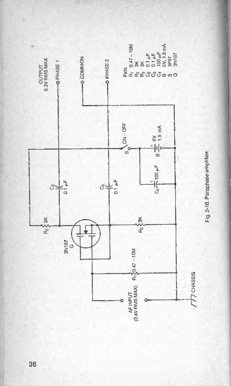
PARAPHASE AMPLIFIERWhen the demands for close balance are not so stringent, a
paraphase inverter may be used in place of the 2 -device phaseinverter just described. A suitable paraphase-type circuit is
33

IC0.
1 µF
AF
INP
UT
(0.1
V R
MS
MA
X)
R1M
R2
3N18
7Qi
R3
R9
1800
0.05
µF
1.5M
470K
R4
270
C2
50 /I
F
/ /C
HA
SS
IS
Par
ts
R1
1M
R2
470K
R3
1.5M
R4
270
R5
1M
R6
470K
R7
1.5M
C3
50µF
R8
270
C4
0.05
µFR
g18
00C
5 0.
05µF
R10
180
0C
6 0.
05µF
R11
500
KB
6V. 3
.5 m
A
R12
470
KS
SP
ST
C1
0.1
/IFQ
1 3N
187
R5
1M
R6
470K
R8
270
C/3
"-' 5
0 µ.
F
R7
1.5M
02R
14 1
800
3N18
7
C5
R11
10N
- O
FF
S
B--
6V _3.
5 m
AT
0.05
µF
500K
BA
LAN
CE
R12
470K
C2
50µF
Q2
3N18
7F
ig. 2
-9. D
ual-m
OsF
ET
pha
se in
vert
er.
0 05
µF
O P
HA
SE
1
OU
TP
UT -0
CO
MM
ON
O P
HA
SE
2

shown in Fig. 2-10. An obvious advantage of such a circuit is itsuse of just one active device.
In this arrangement, a single 3N187 MOSFET supplies eachcomponent of the output signal. Because this is acommon -source circuit, the applied signal undergoes a 180°phase shift at the drain output ( junction of R2 and C2) and nophase shift ( 0°) at the source output ( junction of R3 and C3). Inmost instances, R2 and R3 will be identical; sometimes,however, a particular MOSFET will need adjustment of one ofthese resistances, usually R3, for identical phase -1 and phase -2output voltages.
Current drain from the 6V source is approximately 1.5 mA.The maximum input signal amplitude before output peakclipping is 0.4V RMS. The corresponding maximum outputsignal voltage is 0.3V RMS. The open -circuit voltage gaintherefore is 0.75, somewhat like that of a source follower. Theinput resistance of the stage is largely the resistance ofgate -to -ground resistor RI. For most applications, 0.47M willbe a satisfactory value for R,; for higher input resistance,however, up to 10M may be employed, at some risk of straypickup and pronounced hand -capacitance effects. If desired.fixed resistor RI may be replaced with a potentiometer.
GATED -ON AMPLIFIERFigure 2-11 shows one type of circuit in which an amplifier
is switched on by means of a gating signal; the amplifierautomatically switches off, as far as signal transfer isconcerned, when the gating signal passes. In thiscommon -source circuit, negative bias is applied to gate 2 of theMOSFET by 1.5V source B, through the voltage divider R3-R4.This bias is sufficient to cut the MOSFET off, with normalnegative bias supplied to gate 1 through the voltage dropacross source resistor R5. In the cutoff condition, the amplifiercan pass no signal.
When subsequently a 3V trigger or gating voltage isapplied to the trigger input terminals, enough voltage isdeveloped by the R2-R3 voltage divider to buck the cutoff biasof gate 2 and allow the amplifier to operate. A signal then istransmitted between the amplifier input and output with anopen -circuit voltage gain of 5. When the 3V potential isremoved, the MOSFET resumes its cutoff condition, and theoutput disappears.
Current drain from the 12V source B2 is approximately 0.5mA. Current drain from the cutoff -bias source B, isapproximately 2.8 mA. The maximum input signal voltage
35
0)
R2
Z 3
KC
2
OU
TP
UT
0.3V
RM
S M
AX
3N18
70
AF
INP
UT
(0.4
V R
MS
MA
X)
Ca
R0
47 -
10M
/ f /
CH
AS
SIS
R3
3K
0.1
µF
S\ O
N-O
FF
iC4
1 00
p..
F
+6V
B - T
1.5
mA
Fig
. 2-1
0. P
arap
hase
am
plifi
er.
0 P
HA
SE
1
0 C
OM
MO
N
0 P
HA
SE
2
Par
ts
R1
0.47
-10M
R2
3KR
33K
G2
0.1µ
FG
30.
1µF
C4
1 00
p.F
B6V
, 1.5
mA
SS
PS
T
O3N
187

Par
tsR
t1M
C1
0.05
µFR
227
0KC
250
R3
270K
C3
0.05
µF
F14
270K
B1
1.5V
R5
270
B2
12V
, 0.5
mA
Rs
20K
03N
187
1M GA
IN
AF
INP
UT
(0.2
V R
MS
MA
X A
T G
1)
/CH
AS
SIS
R4
270K
Si
270K
R3
270K
Bi.T
1.5V
3-V
TR
IGG
ER
INP
UT
Fig
. 2-1
1. G
ated
-on
am
plifi
er.
3N18
70
11-
R5
270
C2T
50µF
ON
-OF
F
R6
20K
C3 IE
0.05
µF
AF
OU
TP
UT
(1V
RM
S M
AX
)
O

before output clipping is 0.2V RMS at gate 1 of the MOSFET ( higher amplitude signals are reduced to this maximum by
appropriate settings of gain -control potentiometer R,). The corresponding maximum output signal voltage is 1V RMS. The
input resistance of the circuit is approximately 1M, determined largely by the full resistance of potentiometer RI;
but this may be increased, if desired, by using a higher -resistance potentiometer. However, at the higher
resistances, there is increased risk of stray pickup. A gated -on amplifier has various applications in automatic
control equipment and measuring instruments.
GATED -OFF AMPLIFIER Figure 2-12 shows one type of circuit (the opposite of that described in the preceding section) in which an amplifier is switched off by means of a gating signal; the amplifier
automatically switches on, as far as signal transfer is concerned, when the gating signal passes. In this
common -source circuit, negative bias is applied to gate 2 of the MOSFET, by the gating voltage divider R2 -R3, to pinch off the MOSFET. When this gating bias is absent, the MOSFET is
normally biased by the negative voltage ( resulting from the flow of drain current through source resistor R4) applied to gate 1.
When no signal is applied to the trigger input terminals, the amplifier transmits a signal between its input and output
with an open -circuit voltage gain of 5. When a 2V potential is applied to the trigger input terminals in the polarity shown
here, however, the MOSFET is pinched off and the output signal vanishes. When the 2V gating signal is removed, the amplifier
automatically resumes operation. Current drain from the 12V source is approximately 0.5
mA. The maximum input signal voltage before output peak clipping is 0.2V RMS at gate 1 of the MOSFET (higher amplitude signals are reduced to this maximum by appropriate settings
of gain -control potentiometer Ri). The corresponding maximum output signal voltage is 1V RMS. The input resistance of the circuit is approximately 1M, determined
largely by the full resistance of potentiometer RI; but this may be increased, if desired, by using a higher resistance
potentiometer. However, at the higher resistance, there is increased risk of stray pickup.
Like the gated -on amplifier described in the preceding section, this gated -off amplifier has various applications in
automatic control equipment and measuring instruments.
38

i
005µ
F
AF
INP
UT
(0.2
V R
MS
MA
XA
T G
1)
/ ) 7
CH
AS
SIS
to
1MR1
GA
IN
0
2V T
RIG
GE
R IN
PU
T
R2
270K
3N18
7
R3
270K
R4
270
Par
ts
R1
1M
R2
270K
R3
270K
R4
270
R5
20K
C1
0.05
µFC
250
µFC
30.
05µF
B12
V, 0
.5 M
AS
SP
ST
Q3N
187
C2I
N
50 µ
F
Fig
. 2-1
2. G
ated
-of
f am
plifi
er.
R5
20K
O
0.05
AF
ON
-OF
F
12V
0 5
mA
AF
OU
TP
UT
(1V
RM
S M
AX
)
0

LC -TUNED LOW-PASS AMPLIFIER Amplifiers may be tuned in various ways to pass certain
frequencies and reject others. Figures 2-13 to 2-20 show circuits of such amplifiers. The advantages of tuned amplifiers
over plain, passive tuned circuits or filters are: (1) high input impedance, (2) voltage gain, (3) isolation of the tuning
elements from external circuits, and (4) substitution in some instances of compact RC -tuned elements for bulkier inductors.
Figure 2-13A shows the circuit of an amplifier having the characteristics of a low-pass filter. Figure 2-13B shows the
amplifier response; here, fc is the cutoff frequency. This
response is obtained by incorporating an LC -type high-pass filter section in the negative feedback loop between the drain
output and gate -1 input circuit of the MOSFET, with the result that negative feedback occurs at all frequencies above fe,
canceling the gain at those frequencies, whereas the amplifier has approximately full gain below IC.
Inductance L and capacitance C2 are chosen for the desired cutoff frequency I. according to the following
equations, in which L is in henrys, C2 in farads, and f in hertz:
104 L - 12.6f,
1 C2 - 12.6f, x 104
(Eq. 2-3)
(Eq. 2-4)
From Eq. 2-3, it is seen that for a cutoff frequency of 1000 Hz, L = 794 mH; and from Eq. 2-4, C2 = 0.0079 µF. Inductor L
should be of as high quality as practicable to insure that it has high Q; otherwise, the filter rolloff will not be sharp.
In the basic circuit, MOSFET Q receives its negative gate -1
bias from the voltage drop resulting from the flow of drain current through source resistor R5, and its positive gate -2 bias
from voltage divider R3-R4. With an individual MOSFET, R4
may need some adjustment for linear response of the amplifier. Current drain from the 6V supply is approximately 2
mA. Open -circuit voltage gain of the circuit is 10 in the passband. The maximum input signal voltage before output
peak clipping is 0.1V RMS at gate 1 ( higher amplitude signals are reduced to this maximum value by appropriate settings of
potentiometer Ri). The corresponding maximum output signal voltage is 1V RMS.
40

Par
ts
R1
1MR
210
KR
347
0KR
41.
8MR
533
0R
618
00C
10.
1 µF
C2
SE
E T
EX
TC
3 50
µFC
40.
1 µF
B6V
, 2 m
AL
SE
E T
EX
TQ
3N18
7
0.1
µF
AF
INP
UT
(0.1
V R
MS
MA
XA
T G
1)O
/77C
HA
SS
IS41
.
1M GA
IN
R2
10K
L
C2 )I
3N18
7
(A)
CIR
CU
IT
fc I
,0
FR
EQ
UE
NC
Y
(B)
RE
SP
ON
SE
Fig
. 2-1
3. L
C -
tune
d lo
w-p
ass
ampl
ifier
.
50 µ
F
R6
1800
ItB
6V 2 m
A
0.1
µF
AF
OU
TP
UT
(1V
RM
S M
AX
)

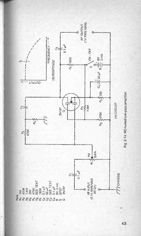
RC -TUNED LOW-PASS AMPLIFIER Figure 2-14A shows the circuit of an amplifier having
the characteristics of a low-pass filter; but, unlike the preceding unit, this amplifier is tuned by means
of a resistance-capacitance section ( R6-C3), instead of
an inductance-capacitance section. The advantage is compactness (inductors are bulky for AF tuning and are
subject to pickup) ;
however, the response shown in Fig. 2-14B is not so sharp as that of the LC -tuned amplifier ( see, for
comparison, Fig. 2-13B). In Fig. 2-14B, fc is the cutoff frequency.
In this circuit, low-pass response is obtained by incorporating an RC -type high-pass filter section R6-C, in the
negative feedback loop between the drain output and gate -1
input circuit of the MOSFET, with the result that negative feedback occurs at all frequencies above f, canceling the gain
at those frequencies, whereas the amplifier has approximately full gain below f
Resistance R6 and capacitance C3 are chosen for the desired cutoff frequency according to the following equations,
in which R6 is in ohms, C3 in farads, and fa in hertz:
1 R6 - 6.28f,C,
1
C3 6.28f R6
(Eq. 2-5)
(Eq. 2-6)
From Eq. 2-5, it is seen that for a cutoff frequency of 1000 Hz and a selected value of C = 0.01 itLF, R6 = 15,924n. In general,
it will be better to select a capacitance, as above, and prune the resistance for the exact R6 value from Eq. 2-5.
In the basic circuit, MOSFET Q receives its negative gate -1
bias from the voltage drop resulting from the flow of drain current through source resistor R4, and its positive gate -2 bias
from voltage divider R2 -R3. With an individual MOSFET resistance R3 may need some adjustment for linear response
of the amplifier. Current drain from the 6V supply is approximately 2 mA. Open -circuit voltage gain of the circuit is approximately 10 in the passband. The maximum input signal
voltage before output peak clipping is 0.1V RMS (higher amplitude signals are reduced to this maximum by
appropriate settings of potentiometer R,). The corresponding maximum output signal voltage is 1V RMS.
42
Par
ts
R1
1MR
247
0KR
,31.
8MR4
330
R5
470K
FI6
SE
E T
EX
TR
718
00C
I0.
1 i.L
F
C2
50µF
C3
SE
E T
EX
TC
40.
1 µF
B6V
, 2 m
AS
SP
ST
O3N
187
C1 K
0.1
AF
INP
UT
(0.1
V R
MS
MA
XA
T G
1)
O
/77
CH
AS
SIS
A CO
GA
IN
Rs
1.8M
247
0KR
433
050
p.F
6yrn
f_
.2A
fe
o_ 7
'Ps
I\,.
FR
EQ
UE
NC
Y
(B)
RE
SP
ON
SE
0.1
1800 O
N -
OF
F
(A)
CIR
CU
IT
Fig
. 2-1
4. R
C -
tune
d lo
w-p
ass
ampl
ifier
.
AF
OU
TP
UT
(1V
RM
S M
AX
)

LC -TUNED HIGH-PASS AMPLIFIER Figure 2-15A shows the circuit of an amplifier having the
characteristics of a high-pass filter. Figure 2-15B shows the amplifier response; here, fe is the cutoff frequency. This response is obtained by incorporating an LC -type low-pass
filter section L -C2 in the negative feedback loop between the drain output and gate -1 input circuit of the MOSFET, with the result that negative feedback occurs at all frequencies below
f,, canceling the gain at those frequencies, whereas the amplifier has approximately full gain above f,
Inductance L and capacitance C2 are chosen for the desired cutoff frequency 1, according to the following
equations, in which L is in henrys, C in farads, and fc in hertz:
10' L
3.14f,.
1 C2
3.14f, x 10'
( Eq. 2-7)
(Eq. 2-8)
From Eq. 2-7, it is seen that for a cutoff frequency of 1000 Hz, L = 3.18H; and from Eq. 2-8, C2 = 0.032 µF. Inductor L should
be of as high quality as practicable to insure that it has high Q; otherwise, the filter rolloff will not be sharp.
In the basic circuit, MOSFET Q receives its negative gate -1 bias from the voltage drop resulting from the flow of drain
current through source resistor R4, and its positive gate -2 bias from voltage divider R2-R3. With an individual MOSFET,
resistance R3 may need some adjustment for linear response of the amplifier. Current drain from the 6V supply is
approximately 2 mA. Open -circuit voltage gain of the circuit is approximately 10 in the passband. The maximum input signal
voltage before output peak clipping is 0.1V RMS at gate 1
(higher amplitude signals are reduced to this maximum by appropriate settings of potentiometer RI). The corresponding
maximum output signal voltage is 1V RMS.
RC -TUNED HIGH-PASS AMPLIFIER Figure 2-16A shows the circuit of an amplifier having the
characteristics of a high-pass filter; but, unlike the unit described in the preceding section, this amplifier is tuned by
means of a resistance-capacitance section ( R3-C2), instead of an inductance-capacitance section. The advantage is
44

Par
ts
R1
1MC
310
0µF
R2
470K
C4
0.1
µFR
31.
8MC
550
µFR
433
0B
6V, 2
mA
R5
10K
LS
EE
TE
XT
Fie
,
C1
1800
S
0.1
µFQ
SP
ST
3N18
7R
510
K
C2
SE
E T
EX
T
3N18
7
Ci
AF
INP
UT
(0.1
V R
MS
MA
XR
iA
T G
1)
O
1M 4 GA
IN
100
0
fc
R3
R6
1800
1.8M
ELE
CS
FR
EQ
UE
NC
Y -
-
(B)
RE
SP
ON
SE
C4
0.1µ
F
ON
-O
FF
-r
R2
470K
R4
C5
50 µ
.c B
--IL
6V 2 m
A
AF
OU
TP
UT
(1V
RM
S M
AX
)
//C
HA
SS
IS
rs
(A)
CIR
CU
IT
Fig
. 2-1
5. L
C -
tune
d hi
gh-p
ass
ampl
ifier
.

Par
ts
R1
1 M
C2
SE
E T
EX
TR
210
KC
310
0 µ
F
R3
SE
E T
EX
T C
40.
1 /./
F
R4
470K
C5
50µF
R5
1.8M
B6V
, 2 m
A
R6
330
SS
PS
T
R7
1800
03N
187
C1
0.1
/IFR
2
Cl
0.1
1.i.F
AF
INP
UT
(0.1
V R
MS
MA
XA
T G
1)0
1M
10K
3N18
7
R3
o'V
NA
,
C3
tfc
1 H -
I- -
- -
- -
-= o_
1
H/
=/
010
0
+µF
FR
EQ
UE
NC
Y -
(B)
RE
SP
ON
SE
C4
R18
00
GA
IN
RS
1 8M
Rd
470K
R6
330
50 p
.F
ON
-O
FF
If6V
B--
T 2
mA
0.1
kLF
AF
OU
TP
UT
(1V
RM
S M
AX
)
0
/ / /C
HA
SS
IS
Fig
. 2-1
6. R
C -
tune
d hi
gh-p
ass
ampl
ifier
.

compactness ( inductors for AF tuning are bulky and subject topickup) ; however, the response shown in Fig. 2-16B is not sosharp as that of the LC -tuned amplifier (see, for comparison,Fig. 2-15B). In Fig. 2-16B, fe is the cutoff frequency.
In this circuit, high-pass response is obtained byincorporating an RC -type low-pass filter section ( R3-C2) in thenegative feedback loop between the drain output and gate -1input circuit of the MOSFET, with the result that negativefeedback occurs at all frequencies below f canceling the gainat those frequencies, whereas the amplifier has approximatelyfull gain above f,
Resistance R3 and capacitance C2 are chosen for thedesired cutoff frequency according to the following equations,in which R3 is in ohms, C2 in farads, and fc in hertz:
1
R3 6.28f,C2
C2 - 6.28f R3
(Eq. 2-9)
(Eq. 2-10)
From Eq. 2-9, it is seen that for a cutoff frequency of 1000 Hzand a selected capacitance C2 of 0.1 p,F, resistance R3 equals159211. In general, it will be better to select a capacitance, asabove, and prune the resistance for the exact required R3value from Eq. 2-9.
In the basic circuit, MOSFET Q receives its negative gate -1bias from the voltage drop resulting from the flow of draincurrent through source resistor R6, and its positive gate -2 biasfrom voltage divider R4-R5. With an individual MOSFET,resistance R5 may need some adjustment for linear responseof the amplifier. Current drain from the 6V supply B isapproximately 2 mA. Open -circuit voltage gain of the circuit isapproximately 10 in the passband. The maximum input signalvoltage before output peak clipping is 0.1V RMS (higheramplitude signals are reduced to this maximum byappropriate settings of potentiometer R1). The correspondingmaximum output signal voltage is 1V Rms.
LC -TUNED PEAK AMPLIFIERFigure 2-17A shows the circuit of a sharply tuned peak
amplifier that tends to pass a single frequency (signal peak).Such an amplifier is useful in null detection, signal separation,
47

03P
arts
R1
1MC
3S
EE
TE
XT
R2
10K
C4
100µ
FR
347
0KC
50.
1 iL
FR
41.
8MB
6V, 2
mA
R5
330
SS
PS
T
R6
1800
LS
EE
TE
XT
C1
0.1
/IFQ
3N18
7
C2
50µF
C1
F0.
1
AF
AF
INP
UT
(0.1
V R
MS
MA
XA
T G
1)0
/ / /C
HA
SS
IS
R
1M
j
10K
3N18
7a
0000
00
C3
1C
410
0 µF
H 0
fr A I% I
FR
EQ
UE
NC
Y -
-
(B)
RE
SP
ON
SE
Cs
`GA
INR
4
6218
00
1.8M
R3
470K
R5
330
C2
T50
/AF
B1:
1-6V
T-2
mA
(A)
CIR
CU
IT
Fig
. 2-1
7. L
C -
tune
d pe
ak a
mpl
ifier
.
ON
-OF
F
0.1
/IF
AF
OU
TP
UT
(1V
RM
S M
AX
)

distortion measurements, and similar applications in which itis desired to pass a single frequency while eliminating allothers. In this circuit, frequency peaking is obtained by in-corporating a signal absorption circuit ( parallel -resonantcircuit L -C3) in the negative feedback loop between the drainoutput and gate -1 input section of the MOSFET, with the resultthat negative feedback occurs at all frequencies above andbelow the resonant frequency (1, in Fig. 2-17B) , which isabsorbed by the L-C3 combination, canceling the gain at thosefrequencies, whereas the amplifier has approximately fullgain at frequency f, . Figure 2-17B shows this response.
Inductance L and capacitance C3 are chosen for thedesired peak frequency according to the following equations,in which L is in henrys, C in farads, and Jr in hertz:
1L =
39.539.5 3
C3 = 39.5f2, L
From Eq. 2-12, it is seen that for a resonant ( peak) frequencyof 1000 Hz and a selected inductance of 10H, capacitance C3equals 0.0025 µF. In general, it will be better to select aninductance, as above, and prune the capacitance for the exactrequired C3 value from Eq. 2-12.
In the basic circuit, MOSFET Q receives its negative gate -1bias from the voltage drop resulting from the flow of draincurrent through source resistor R5, and its positive gate -2 biasfrom voltage divider R3 -R4. With an individual MOSFET,resistance R4 may need some adjustment for linear responseof the amplifier. Current drain from the 6V supply isapproximately 2 mA. Open -circuit voltage gain of the circuit isapproximately 10 at the peak (fr in Fig. 2-17B). The maximuminput signal voltage before output peak clipping is 0.1V RMS(higher amplitude signals are reduced to this maximum byappropriate settings of potentiometer R1). The correspondingmaximum output signal voltage is 1V RMS.
RC -TUNED PEAK AMPLIFIERFigure 2-18A shows the circuit of a sharply tuned
peak amplifier having characteristics similar to theone just described: but, unlike that unit, this amplifier istuned by means of a resistance-capacitance section
49

CJ1
Par
ts0
Ri
1M02
R2
10K
03
133
C4
*
R4
.C
5 10
µFR
5C
60.
1 µF
R6
470K
C7
50µF
R7
1.8M
B6V
, 2 m
A
Re
330
SS
PS
TR
3
R3
1800
03N
187
C1
0.1
ALF
SE
E T
EX
T
AF
INP
UT
(0.1
V R
MS
MA
XF
it
AT
G1)
0
R2
10K
M
GA
IN
-/77
CH
AS
SIS
3N18
7
1.8M
R5
C5
I-1-
S
IR
6 47
0K13
833
0 C
750
/IFI
B-+
6V
T-2
mA
10µF
1800
7 0_ 0
fr A
FR
EQ
UE
NC
Y -
(B)
RE
SP
ON
SE
C6
0.1
;IF
AF
OU
TP
UT
(1V
RM
S M
AX
)
(A)
CIR
CU
IT
ON
-OF
F
Fig
. 2-1
8. R
C -
tune
d pe
ak a
mpl
ifier
.

C2-C3-C4-R3-R4-R5, instead of an inductance-capacitance section. The advantage is compactness ( AF
inductors are bulky and are subject to pickup) . The responseof the amplifier is shown in Fig. 2-18B, where 1, is the peakfrequency.
In this circuit, peaking is obtained by incorporating a nullcircuit in the negative feedback loop between the drain outputand gate -1 input section of the MOSFET, with the result thatnegative feedback occurs at all frequencies except the nullfrequency of the RC network (fr in Fig. 2-18B), which isremoved by the RC network, canceling the gain at thosefrequencies, whereas the amplifier has full gain at frequencyfr Figure 2-18B shows this response.
The null circuit, which tunes the amplifier, is a parallel -Tnetwork ( C2-C3-C4-R3- R4- R 5) . In this network,C2 = C3 = 0.5C4, and R3 = R5 = 2R4. When these relationshipsare preserved, the null frequency of the network, andtherefore the peak frequency of the amplifier, may bedetermined by the equation
Jr6.28R13C2
(Eq. 2-13)
where J. is in hertz, R3 in ohms, and C2 in farads.From Eq. 2-13, it is seen that for a parallel -T circuit in
which C2 and C3 are 0.1 /IF, C4 = 2C3 = 0.2 I.LF, R3 and R5 areeach 159211, and R4 = 0.5R3 = 79652, and the null frequency is1000 Hz (the peak frequency J. of the amplifier). In general, itis best to select the three capacitances (C2 = C3 = 0.5C4) andthen to adjust the resistances to exact values , R, = R5 =2R4) asrequired. The following equations-in which R is in ohms, C infarads, and 1, in hertz-will help:
1R3 = R5 -
6.28f ,C2(Eq. 2-14)
R4 = 0.5R3 (from Eq. 2-14) (Eq. 2-15)
Resistances and capacitances must have exact values.The sharpness of the selectivity curve in Fig. 2-18B will dependupon the closeness with which these components meetspecified values. The circuit may be made continuously tuna-ble by using a 3 -gang potentiometer for R,- R4- R5 andswitching the capacitors in groups of three to change Ire-quency ranges. In this way, the amplifier can be given tuning
51

ranges of 20-200, 200-2000, and 2000-20,000 Hz, to cover the audio -frequency spectrum. In this circuit, MOSFET Q receives its negative gate -1 bias
from the voltage drop resulting from the flow of drain current through source resistor R8, and its positive gate -2 bias from voltage divider R6-R,. With an individual MOSFET, resistance
R, may need some adjustment for linear response of the amplifier. Current drain from the 6V supply is approximately 2
mA. Open -circuit voltage gain is approximately 10 at the peak ( jr in Fig. 2-18B). The maximum input signal voltage before
output peak clipping is 0.1V RMS (higher amplitude signals are reduced to this maximum by appropriate settings of
potentiometer R,). The corresponding maximum output signal voltage is 1V RMS.
LC -TUNED NOTCH AMPLIFIER Figure 2-19A shows the circuit of a sharply tuned bandstop
amplifier that tends to suppress a single frequency, i.e., to produce a notch or slot in the amplifier frequency response.
Such an amplifier has applications in signal removal, distortion measurement, and similar uses where it is desired
to remove a single frequency while passing all others. In this circuit, signal removal is accomplished by incorporating a
parallel -resonant (wavetrap) circuit L-05 between the two stages of the MOSFET amplifier.
Inductance L and capacitance C5 are chosen for the desired slot frequency (1, in Fig. 2-19B) according to the
following equations, in which L is in henrys, C in farads, and f,. in hertz:
1 L = 39.5f ,C5 (Eq. 2-16)
1 C5 = 39.5f, L (Eq. 2-17)
In most instances, the inductor will have a fixed value. This means that L thus must be chosen and capacitance C5
determined in terms of L. For example, if we start with an available 2H inductor and desire a slot frequency of 1000 Hz,
capacitance C5 (from Eq. 2-17) will be 0.0126 µF. To determine the frequency of any available inductor and capacitor, use the
following equation, in which C5 is in farads, L in henrys, and Jr in hertz:
Jr - 6.28\1-07 (Eq. 2-18)
52

Par
ts81
1M8,
933
0R
247
0KR
10 1
800
R3
1 8M
GI
0.1
/IFR
433
002
50 µ
FR
518
00C
310
µFR
647
0KC
41µ
FR
747
0KC
6S
EE
R8
1,8M
TE
XT
C6
50µF 3N
187
C1
0 1
µF
0A
F IN
PU
T(0
1 R
MS
R1
GA
INM
AX
AT
G1)
//C
HA
SS
IS01
FH
H-
R5
1800
R47
0K
C3,
10 'I
FO
N -
+50
IO
FF
R2;
IF47
0K R
4 33
06V
B=
4 m
A
C2
C7
0.1
µFB
6V,4
mA
1-S
SP
ST
aS
.B 0
.1 µ
FI -
LS
EE
TE
XT
001
3N18
7Q
23N
187
R3
1.8M
(A)
CIR
CU
IT
Fig
. 2-1
9. L
C -
tune
d no
tch
ampl
ifier
.
/I
/ /
fry FR
EQ
UE
NC
Y -
- -
(B)
RE
SP
ON
SE
C8-
50 A
LF
018
00
0.1
µF
AF
OU
TP
UT
(1V
RM
S M
AX
)
0

Thus. for an inductance of 10H and capacitance C5 of 0.002 AF,
= 1126 Hz. For maximum sharpness of the response curve ( Fig. 2-19B), the Q of inductor L must be high.
In this circuit, MOSFET Q, receives its negative gate -1 bias from the voltage drop resulting from the drain current through
source resistor R4, and its positive gate -2 bias from voltage divider R7- R.,. Similarly, MOSFET Q2 receives its negative
gate -1 bias from the voltage drop across source resistor R6,
and its positive gate -2 bias from voltage divider R2- R 8.
With individual mosFETs, resistors R3 and R8 may need some
adjustment for linear operation of the amplifier. Current drain from the 6V supply is approximately 4 mA. Open -circuit
voltage gain is approximately 90 to 100 in the passband, its exact value depending upon losses in inductor L. The
maximum input signal voltage before output peak clipping is 10 mV RMS (higher amplitude signals are reduced to this
maximum by appropriate settings of potentiometer R1). The corresponding maximum output signal voltage is 1V RMS.
RC -TUNED NOTCH AMPLIFIER Figure 2-20A shows the circuit of a sharply tuned notch
amplifier having characteristics similar to those of the amplifier just described; but, unlike the unit just described,
this amplifier is tuned by means of a resistance-capacitance null network ( C4-05-C6-R6- R7--- R 8)
, instead of an
inductance-capacitance section. The advantage is compactness, freedom from pickup, and adaptability to
continuous tuning by varying the resistors. The response of the amplifier is shown by Fig. 2-20B, where f is the notch
frequency ( also called slot frequency). The null circuit, which tunes the amplifier, is a parallel -T network ( C4-C,-C6-R6-R2- R8)
.
In this network, C4 = C5 = 0.5C6, and R, = R, = 2R8. When these relationships
are preserved, the null frequency of the network, and therefore the notch frequency in Fig. 2-20B, may be
determined with the aid of the following equation (in which C4
is in farads, R6 in ohms, and f in hertz) :
1 Jr 6.28R6C4 (Eq. 2-19)
From Eq. 2-19, it is seen that for a parallel -T circuit in which C4 and C5 are each 0.005 ktF, C6 = 0.01 µF, R6 and R, are
each 10001/, and R8 = 5000, the null frequency is 31.85 kHz. In general, it is best to select the three capacitances
( C4 = C5 = 0.5C6) and make up the exact values of resistance (R6 = R, = 2R8), as required. The following equations-in
54

Par
tsR
11M
R13
180
0S
SP
ST
R2
470K
CI
0.1
;IFQ
13N
187
R3
1.8M
C2
50µF
02 3
N18
733
0C
3 10
µF.
TEXT
R5
1800
C4
SE
E
R6
C5
R7
C6
*
R8
C7
50µF
R9
10M
C8
0.1
LLF
Rip
470
KC
g 10
µFR
11 1
.8M
B6V
, 4 m
A
R12
330
3N18
7Q
1
0.1J
Ci ALF
0A
F IN
PU
T(1
0 m
V R
MS
MA
X A
T G
1)
0
R1
GA
IN R2
R
C3
C4
+1E
-110
µF
R6
R7
C5
R8
R5
1800
/ / /C
HA
SS
IS
(Ti
1 8M
C2
-±47
0K13
433
0
T50
µF
(A)
CIR
CU
IT
/
fr1 V
FR
EQ
UE
NC
Y -
(B)
RE
SP
ON
SE
C8
0.1
ALF
1800
R9
C9
AF
+1(
(0O
UT
PU
T9V
RM
SM
AX
)10
ALF
/ )O
N-O
FF
21_F
6V 4 m
A
IF
ig. 2
-20.
RC
-tu
ned
notc
h am
plifi
er.

R6 = R, = 6.281rC4 ( Eq. 2-20)
R8 = 0.5R6 ( from Eq. 2-20) (Eq. 2-21)
Resistances and capacitances must have exact values. The sharpness of the selectivity curve in Fig. 2-20B will depend
upon the closeness with which these components meet specified values. The circuit may be made continuously
tunable by using a 3 -gang potentiometer for R6- R7-R6 and switching the capacitors in groups of three to change
frequency bands. In this way, the amplifier can be given tuning ranges, for example, of 20-200, 200-2000, and
2000-20,000 Hz. In this circuit, MOSFET Q, receives its negative gate -1 bias
from the voltage drop resulting from the flow of drain current through source resistor R4, and its positive gate -2 bias from voltage divider R2 -R3. Similarly, MOSFET Q2 receives its
negative gate -1 bias from the voltage drop across source resistor R12, and its positive gate -2 bias from voltage divider
R,0-R . With individual MOSFETS, resistors R3 and R may need some adjustment for linear operation of the amplifier.
Current drain from the 6V supply is approximately 4 mA. Open -circuit voltage gain is approximately 80 to 90 in the
passband, depending upon individual mosFETs and the amount of attenuation introduced by an individual parallel -T network.
The maximum input signal voltage before output peak clipping is 10 mV RMS ( higher amplitude signals are reduced to this
maximum by appropriate settings of potentiometer R,) .
The corresponding maximum output voltage is 0.8V to 0.9V RMS.
which R is in ohms, C in farads, and f, in hertz-will help: 1
HEADPHONE AMPLIFIER Although an amplifier for headphones is a relatively
simple device, its operation also can be improved through the
use of a MOSFET. The MOSFET affords very high input impedance and extreme miniaturization. The high impedance
insures that the headphones, whether employed for communications or instrumentation, will present virtually no
load to the signal source. This is especially important when magnetic headphones or a magnetic earpiece is used.
Figure 2-21 shows the circuit of a simple, inexpensive amplifier for high -resistance magnetic headphones. The input
resistance of the circuit is approximately 1M, determined principally by the full resistance of volume control
potentiometer R,. A higher resistance may be employed, at some risk of stray pickup.
56

7-1K
"="-
T":
717r
e'77
:77,
_
.-
AF
INP
UT
(0 1
V R
MS
MA
X A
T G
l)
1M VO
LUM
E
3N18
7
R3
Par
ts
R1
1MR
2 16
00R
3 82
00R
4 27
0C
I0.
1 p.
FC
2 50
µFB
9V, 2
.6 m
AS
SP
ST
Q3N
187
8200
R16
00R
427
0C
250
µF
//C
HA
SS
IS01
Fig
. 2-2
1. H
eadp
hone
am
plifi
er.
HIG
H -
RE
SIS
TA
NC
EM
AG
NE
TIC
HE
AD
PH
ON
ES
ON
-OF
F
9V 2 6
mA
T-

In this circuit, the MOSFET receives its negative gate -1 bias from the voltage drop resulting from the flow of drain current
through source resistor R4, and its positive gate -2 bias from _voltage divider R2 -1i3. With an individual MOSFET, resistance
R3 may need some adjustment for low distortion in the circuit. When a pair of 20000 magnetic headphones is used, the
maximum input signal voltage before output peak clipping is 0.1V RMS ( higher amplitude signals are reduced to this
maximum by appropriate settings of potentiometer Rd. The corresponding maximum output voltage across the headphone
load is 1V RMS. Under these conditions, the voltage gain is 10. A 0.5 mV RMS input signal at gate 1 of the 3N187 MOSFET gives a
just barely audible signal in the headphones. Current drain from the 9V supply is approximately 2.6 mA.
PEAKED -RESPONSE HEADPHONE AMPLIFIER Headphones usually have a resonant peak due chiefly to
dimensions of the diaphragm. This peak may be intensified or a more satisfactory one provided simply by tuning the
inductance of the headphones with a suitable capacitance such as C3 in Fig. 2-22. Thus, the headphones may be tuned to a
readily recognizable frequency such as 400 or 1000 Hz, and this will improve code reception, as well as providing additional
signal selectivity. Such resonating of the headphones is advantageous also in the balancing of an AC bridge by means of
headphones. The tuning may be accomplished practically by feeding a
signal of the desired frequency into the input terminals of the amplifier and adjusting a capacitor decade ( connected in
parallel with the headphones) for peak response, as indicated by maximum upswing of an AC electronic voltmeter ( VTVM or
TVM) connected temporarily across the headphones. Or the inductance L of the headphones may be measured with a
suitable AC bridge and the required capacitance calculated with the aid of the following equation, in which L is the
headphone inductance in henrys, C, is the required capacitance in microfarads, and Iris the resonant frequency in
hertz: 1.000.000
CI - 39.5f, L
In all respects other than the tuning of the headphones, this circuit is the same as the simpler one described in the
preceding section. For electrical characteristics, therefore, refer to that section.
(Eq. 2-22)
58

Par
tsR
11M
R2
1600
R3
8200
R4
270
C1
0.1
auF
C2
50µF
C3
SE
E T
EX
TB
9V
, 2.6
mA
S S
PS
TO
3N18
7H
IGH
-R
ES
IST
AN
CE
MA
GN
ET
IC H
EA
DP
HO
NE
S
I(01
ILF
AF
INP
UT
(0.1
V R
MS
MA
XR
1
AT
G1)
0
1M
3N18
7a
4-
VO
LUM
E
R2
R3
1600
8200
270
C2T
50
µF
HIG
H -
RE
SIS
TA
NC
EM
AG
NE
TIC
HE
AD
PH
ON
ES
sO
N-O
FF
=9V
B _
_2.
6 m
A
/7-7
CH
AS
SIS
Fig
. 2-2
2. P
eake
d -r
espo
nse
head
phon
e am
plifi
er.

Chapter 3
DC, RF, and IF Amplifiers
This chapter offers circuits for four DC amplifiers, four RF amplifiers, one video amplifier, and three IF amplifiers. These
circuits will suggest others to experimenters, and the intended applications also will suggest others.
In each of the circuits, unless otherwise indicated on the circuit diagram or in the text, capacitances are in picofarads,
resistances in ohms, and inductances in microhenrys. Resistors are 1/2W, and electrolytic capacitors are 25 working
volts. Because of the electrical characteristics of the MOSFET, most of the circuits are seen to be closely similar to their
vacuum -tube counterparts. Thus, special components such as tapped transistor -type transformers are not required.
For simplicity, batteries are shown for DC supply; however, a well filtered line -operated power supply may be
used instead of a battery. Before undertaking the wiring and operation of any
circuit, read carefully the hints and precautions given in Chapter 1.
DC AMPLIFIER Figure 3-1 shows a simple single-MOSFET circuit for amplifying direct currents. In this arrangement the current of
interest flows through input resistor R,. The voltage drop which accordingly is developed across this resistor is applied
to gate 1 of the 3N187 MOSFET. This causes the MOSFET drain current to increase in accordance with the transconductance
60

3N18
7a
-
DC
INP
UT
R1
+0
100K
6V10
mA
Par
ts
R1
100K
B 6
V, 1
0 m
AS
SP
ST
3N
187
ON
-O
FF
DC
OU
TP
UT
III
Fig
. 3-1
. Cur
rent
am
plifi
er (
DC
).
1
RL
(LO
W4v
RE
SIS
TA
NC
E)

of the device, with the result that the output current, flowing through a low -resistance load, is much greater than the
input current flowing through R,. Gate 2 of the MOSFET is returned to the source.
A residual drain current of approximately 3 mA DC flows in the output circuit, and this quiescent current can be
balanced out of the load device ( such as a meter) ,
when desired, by means of any one of the conventional Dc -bucking circuits. When the input signal voltage drop applied to gate 1 is
1V, the drain current increases to approximately 6 mA. At 1V input, the current through resistor R, is 0.00001A = 0.01 mA,
and for the corresponding drain current change of 3 mA, the resulting current gain is 300. A higher value of input
resistance R, results in a lower input current for the 1V gate -1 signal and a correspondingly higher current gain. Thus, if
R, = 1M, i, = 1 µA, and the current gain is 3000. The circuit has the disadvantage of high input resistance
( high insertion resistance) ; however, this is of no consequence in some applications. A circuit oddity also is the floating
battery B, but this too causes no trouble in most applications of a current amplifier such as this one.
Individual MOSFETS show different values of transconductance, so the circuit you put together can be more
sensitive or less sensitive than the figures given here. Individual calibration therefore is required. The actual
current amplification depends heavily on the value of the load resistance R1, being highest for low R, resistance.
In order to be adaptable to individual MOSFETS, the 6V supply should be capable of supplying 10 mA.
DC VOLTAGE AMPLIFIER It is often desired to amplify a DC voltage without going
into the complication of a chopper -stabilized type of circuit. For modest requirements, the circuit shown in Fig. 3-2 is
recommended. This arrangement is a simple source -follower circuit for
DC signal input and output. It is the simplest DC voltage amplifier. With zero signal at the input terminals, the quiescent drain current produces a static voltage of 0.15V at
the output terminals. ( This is barely discernible on the scale of a 0-10 voltmeter connected to the output terminals; but if it is
objectionable, it may be balanced out with the aid of any one of the conventional DC -bucking circuits.) When the input signal is 1V at gate 1 of the MOSFET ( gain control R, adjusted for
maximum gain), the corresponding voltage at the output terminals is 5.2V. The actual output voltage thus is
5.2-0.15 = 5.05V, and the voltage gain of the amplifier is 5.05.
62

-o
DC
INP
UT
+0
1M GA
INP
arts
RI 1
MR
2 15
KR
3 27
0B
6V, 0
.2 m
AS
SP
ST
3N18
7
R27
0
S/O
N -
OF
F0
B6V 0.
2 m
A
6+D
C O
UT
PU
T
0-
/1/
cr)
Fig
. 3-2
. Vol
tage
am
plifi
er(o
c).

The maximum recommended DC input signal is 1V.
( Higher signal voltages are reduced to this maximum by appropriate settings of potentiometer R,). The corresponding
maximum output signal voltage is 5.05V DC ( after correction). Fcir reduced loading of a DC signal source, the full resistance of
potentiometer R, may be increased. Conversely, for reduced susceptibility to stray pickup, the maximum resistance of this
potentiometer may be reduced. Maximum drain from the 6V supply is approximately 0.2
mA. Individual MOSFE1N will draw different operating current and will also offer different values of transconductance
( affecting the gain figure given here).
DC GALVANOMETER AMPLIFIER The input resistance of a DC galvanometer such as is used
for bridge balancing may be greatly increased with a MOSFET amplifier. Figure 3-3 shows the circuit of a balanced DC amplifier for this purpose. This circuit provides an input
resistance of 1M, determined largely by the full resistance of sensitivity control potentiometer R1.
This amplifier itself consists of a 4 -arm bridge circuit in which the two MOSFETS are in opposite arms. The bridge is
initially balanced, in the manner of an electronic voltmeter, by means of the zero -set potentiometer R5, and galvanometer M is
connected to the bridge output terminals. A DC input signal applied to gate 1 of one of the MOSFETS ( here, Q1) unbalances
the bridge and causes the meter to be deflected from its center -zero position of rest. A positive input signal at the
amplifier input terminals drives the meter upscale; a negative input signal drives the meter downscale.
Meter M may be a 25-0-25 µA or 50-0-50 µA model. The internal resistance of a typical 25-0-25 µA instrument
( Simpson Model 2123) is approximately 180011. The amplifier provides 1M input resistance, thus apparently increasing the
meter resistance 555 times. The increased resistance greatly enhances the sensitivity and resolution of the instrument in
bridge balancing. When potentiometer R5 is adjusted, with zero input signal,
galvanometer M is set exactly to center zero. Then with sensitivity control potentiometer R, set for maximum sensitivity, a +0.25V DC input signal will deflect meter M up to
full scale, whereas a -0.25V will deflect the meter down to full scale.
Drain from the 6V supply is approximately 1.6 mA. Individual MOSFETS may exhibit somewhat different load
current, but will not materially affect operation of the circuit.
64

Par
tsR
1 1M
R2
1 K
R3
100
R4
1KR
5 1K
WW
86V
, 1 6
mA
SS
PS
T3N
187
02 3
N18
7
+0
DC
INP
UT
-0 1/I
3N18
7Qi
1M
Rio S
EN
SIT
IVIT
Y
R51
1K W
WZ
ER
O S
ET
9 D
C O
UT
PU
T 9
L - M
J.,
CE
NT
ER
-Z
ER
OD
CM
ICR
OA
MM
ET
ER
3N18
7
R2
1KR
41K
1
R3
100
Fig
. 3-3
. Dc
galv
anom
eter
am
plifi
er.
/ / /
S/O
N -
OF
F
6Vm
A

DC SOURCE FOLLOWER Figure 3-4 shows a source -follower circuit designed for
direct -current use. Like the familiar AC source follower (and its counterparts, the emitter follower and cathode follower),
this circuit provides "impedance" transformation; that is, it presents a high input resistance to a DC signal source, and a
low output resistance to a load. When the DC input signal e, is zero, the quiescent drain
current of the MOSFET, flowing through source resistor R2, produces a static voltage e0 at the output terminals of 0.75V. In
many cases this initial voltage will be of no concern; in other instances, however, it may easily be balanced out with the aid
of any one of the conventional bucking circuits. When the input signal is e, is 1V, the output signal voltage is 1.65V. This is an output voltage change of 1.65-0.75 = 0.9V, and it represnets a voltage gain of 0.9 for the source follower.
The input resistance of the circuit is 470K, provided chiefly by the resistor R1. The output resistance is 200052, provided
largely by resistor R2. Other values of R, and R2 may be employed, with somewhat different values of output
resistance. If desired, R, may be a gain -control potentiometer. Response of the circuit is approximately linear. Drain from the 6V source is approximately 1 mA. Individual MOSFEIS will show different current drains, as well
as different transconductance values ( this latter affecting the source -follower voltage gain).
GENERAL-PURPOSE RF AMPLIFIER Figure 3-5 shows the circuit of a single -stage outrigger RF
amplifier which can provide substantial signal gain as a preselector or booster for receivers and instruments. The
circuit is tuned with a dual 365 pF variable capacitor C,-C4. With standard plug-in coils, as shown in Fig. 3-5, the tuning
range can be 500 kHz to 30 MHz. Table 3-1 gives winding
Table 3-1. Broadcast -Band Coil Data.
L1 10 turns No. 32 enameled wire closewound around the lower end of L2and insulated from the latter.
L2 130 turns No. 32 enameled wire closewound on a 1 in. diameter form.
L3 130 turns No. 32 enameled wire closewound on a 1 in. diameter form.
L4 12 turns No. 32 enameled wire closewound around the lower end of L3and insulated from the latter.
66

+0
DC
INP
UT
-0 /I/
(3)
Ri
470K
Fig
. 3-4
. Dc
sour
ce fo
llow
er.
S/O
N-
OF
F
1+6V 1
mA
Par
ts
R1
470K
R2
2000
B6V
, 1 m
AS
SP
ST
O3N
187
1+
DC
OU
TP
UT
1

rn OD
RF
INP
UT
L
Jl
TU
NIN
G
3N18
7O
L2-7
00/
Lc:
1.4
365
Par
tsR
160
KR
291
0KR
327
0
C1
365
C2
0.01
i.L.
F
C3
0.01
/IF
C4
365
pFC
50.
01 p
.FB
12V
, 5 m
AR
FC
1 m
HS
SP
ST
3N18
7
C2-
0.01 k.LF
R2
L3R
F O
UT
PU
TL4
C4\
pF-(
341-
e,
910K
60K
R3
270
RF
C
_PM
0 0
SO
N -
OF
F
037-
-,-
0.01
i.LF
1 m
H
/ //
Fig
. 3-5
. Gen
eral
-pur
pose
RF
am
plifi
er.
IB
12V
-5 m
A C
5- 0
.01
µF
I

instructions for coils for the standard broadcast band. Owingto the extremely low value of interelectrode capacitance in theMOSFET, no neutralization is required.
In this circuit, the incoming RF signal, selected by theinput tuned circuit, is presented to gate 1 of the MOSFET; theoutput signal is developed by drain current in the output tunedcircuit. Coaxial jacks (J, and J2) or other suitable terminalslead the signal into and out of the amplifier. The negativegate -1 bias is provided by the voltage drop resulting from theflow of drain current through source resistor R3. Postive gate -2bias is produced by voltage divider RI- R2. With an individualMOSFET, resistor R2 may require some adjustment formaximum amplification. If the amplifier is to be operatedabove the standard broadcast band, shielding isrecommended; i.e., the unit should be enclosed in analuminum box.
Current drain from the 12V supply is approximately 5 mA.An individual MOSFET may show a somewhat different loadcurrent value.
SINGLE -ENDED TRANSMITTER -TYPE RF AMPLIFIERThe circuit given in Fig. 3-6 has an untuned input and a
tuned output. This is the type of circuit found in the exciter andfinal -amplifier stages in transmitters, hence its designationtransmitter -type. The extremely low interelectrodecapacitance of the MOSFET enables this circuit to be operatedwithout neutralization. The circuit may be employed as givenin flea -powered transmitters and experimental equipment.
Tuning is accomplished with the single 100 pF variablecapacitor C5. Standard amateur -band plug-in coils may beused (each coil set contains an L, and L2), or a single L1-L2pair may be wound for a specific frequency, using coil -windinginstructions found in the various radio handbooks. The circuitis entirely conventional and will be familiar to hams andexperimenters, with the exception that MOSFET Q replaces thevacuum tube usually found in this circuit. Link -coupled,low -impedance output is provided by coupling coil L2. In someinstallations, however, capacitive coupling will be desirable,and this can be provided by output capacitor C6, which will be100 to 250 pF, depending upon individual requirements. Whencapacitive output coupling is used, the small coil L2 is omitted.
In this amplifier circuit, the MOSFET receives its negativegate -1 bias from the voltage drop resulting from the flow ofdrain current through source resistor R4, and its positivegate -2 bias from voltage divider R2- R3. With an individualMOSFET, resistance R, may need some adjustment for
69

0
3N18
7Q
C-1
RF
INP
UT
/ /
100 RF
C1 R
1
2.5
mH
1M
R2
B3
TU
NIC
N54
1
100
C6
(SE
E T
EX
T)
RF
OU
TP
UT
RF
C2
g 2.
5 m
H
9100
C2
0.00
2µF
820
R4
270
IX -
- -
":1±
-C
4-0.
002
T
Ca
0.00
2_
18V
/IF.
,,,,
_T6m
Ai
S7O
N-
OF
F
Fig
. 3-6
. Sin
gle
-end
ed tr
ansm
itter
-ty
pe R
F a
mpl
ifier
Par
ts
R1
1ro
R2
820
R3
9100
R4
270
CI
100
C2
0.00
2µF
G3
0 00
2 /IF
C4
0 00
2 tiF
G5
100
C6
SE
E T
EX
TB
18V
. 6 m
AR
FC
1 2.
5 m
HR
FG
2 2.
5 m
HS
SP
ST
Q3N
187

maximum RF output. Maximum current drain from the 18Vsource is approximately 6 mA.
Tuning of the circuit is straightforward: ( 1) Connect a0-10 mA DC meter temporarily in series with the battery andswitch at point X. (2) Close switch S. ( 3) Disconnect any loadfrom the output terminals. (4) Apply the input signal to theinput terminals. (5) Adjust tuning capacitor C5 for minimumdip of the milliammeter reading. ( 6) Connect the externalload, making any adjustments in the coupling ( coil L, orcapacitor C6) to bring the milliammeter reading up to 6 mA.17) Retune C5, if necessary. for resonance.
The RF power output of the amplifier is approximately 36mW. For this output, the driving signal at the input terminalsmust be approximately 0.8V RMS. The circuit may be keyed forcw transmission or amplitude -modulated for voicetransmission, in the usual manner.
PUSH-PULL TRANSMITTER -TYPE RF AMPLIFIERThe RF amplifier circuit shown in Fig. 3-7 is similar to the
one just described and shown in Fig. 3-6, except that the Fig.3-7 circuit employs two MOSFETS in push-pull for increasedpower output and good harmonic cancellation. The generaldescription of the single -ended circuit (preceding section)applies also to this push-pull circuit, as do the tuninginstructions.
In Fig. 3-7, MOSFET Q, receives its negative gate -1 biasfrom the voltage drop resulting from the flow of drain currentthrough source resistor R4, and its positive gate -2 bias fromvoltage divider R7 -R3. Similarly, MOSFET Q2 receives itsnegative gate -1 bias from the voltage drop resulting from theflow of drain current through source resistor R7, and itspositive gate -2 bias from voltage divider R5-1?,. Withindividual MOSFETS, resistors R3 and R, may require someadjustment for maximum RF power output.
The RF power output of the amplifier is approximately 72mW. For this output, the driving signal ( gate 1 to gate 1) mustbe approximately 1.6V RMS. Maximum current drain from the18V source B is approximately 12 mA. The circuit may bekeyed for cw transmission or amplitude -modulated for voicetransmission, in the usual manner.
100 MHz RF AMPLIFIER
Figure 3-8 shows the circuit of a radio -frequency amplifierdesigned especially for operation at 100 MHz. The single 3N187MOSFET is operated, together with its associated components,inside a metal shield box. The circuit, which operates between
71

3N18
701
Par
ts R
i1M
R2A
3982
1000
R4
270
R5
820
R6
9100
R7
270
C1
(DU
AL
100)
C2
0 00
2 µF 18
V12
mA
C3
0 00
2 µF
C4
0 00
2 µF
C5
(DU
AL
100)
B18
V, 1
2 m
AR
FC
1 2.
5 m
HR
FC
2 2.
5 m
H3N
187
023N
187
Fig
. 3-7
. Pus
h-pu
ll tr
ansm
itter
-ty
pe R
F a
mpl
ifier
.

RF
INP
UT
"
rP
arts
R1
470K
C6
0.00
15µF
R2
1.5M
C7
3pF
C1
7 pF
C8
3pF
C2
1-12
pF
B1
1.5V
C3
0.00
1 to
,FB
26V
, 5 m
AC
40.
0015
µFL1
0.15
µHC
1C
5 0.
0015
µFL2
0.22
µH
(FR
OM
._50
0)
/77
-4 oa
I(
SH
IELD
S1,
2 D
PS
TO
3N18
7
3N18
7
~64
ItiliM
PV
RO
IDM
IPE
WA
IWIS
IK
C8
4--
7 pF
L 0.00
15µF
0.15
µH
1 -1
2 pF
R2
AA
&1.
5M
R1
470K
0.00
15µF
FE
ED
TH
RO
UG
H
B2
B1
6V m
A
II I
1.5V
ON
-OF
F
C7.
y3
pF
3pF
Lea
0.22
µHco
C6
0.00
15µF
FE
ED
TH
RO
UG
H
Fig
. 3-8
. 100
MH
z R
F a
mpl
ifier
.
- -
-
RF
OU
TP
UT
-.-(
TO
500
)
/-7-
7
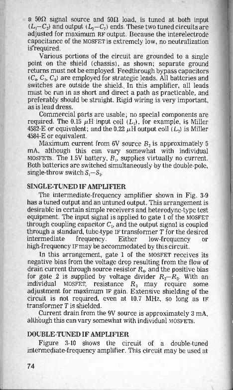
a 5051 signal source and 5051 load, is tuned at both input (LI-C2) and output (L2-C7) ends. These two tuned circuits are
adjusted for maximum RF output. Because the interelectrode capacitance of the MOSFET is extremely low, no neutralization
is -required. Various portions of the circuit are grounded to a single
point on the shield (chassis), as shown; separate ground returns must not be employed. Feedthrough bypass capacitors
( C4, C5, C6) are employed for strategic leads. All batteries and switches are outside the shield.. In this amplifier, all leads
must be run in as short and direct a path as practicable, and preferably should be straight. Rigid wiring is very important,
as is lead dress. Commercial parts are usable; no special components are
required. The 0.15 p..11 input coil (L1), for example, is Miller 4582-E or equivalent; and the 0.22 /LH output coil (L2) is Miller 4584-E or equivalent.
Maximum current from 6V source B2 is approximately 5 mA, although this can vary somewhat with individual
mosFurs. The 1.5V battery, B supplies virtually no current. Both batteries are switched simultaneously by the double -pole,
single -throw switch S1-S2.
SINGLE -TUNED IF AMPLIFIER The intermediate -frequency amplifier shown in Fig. 3-9
has a tuned output and an untuned output. This arrangement is desirable in certain simple receivers and heterodyne -type test
equipment. The input signal is applied to gate 1 of the MOSFET through coupling capacitor CI, and the output signal is coupled through a standard, tube -type IF transformer T for the desired
intermediate frequency. Either low -frequency or high -frequency IF may be accommodated by this circuit.
In this arrangement, gate 1 of the MOSFET receives its negative bias from the voltage drop resulting from the flow of
drain current through source resistor R4, and the positive bias for gate 2 is supplied by voltage divider R2-R3. With an
individual MOSFET, resistance R3 may require some adjustment for maximum IF gain. Extensive shielding of the
circuit is not required, even at 10.7 MHz, so long as IF transformer T is shielded. Current drain from the 9V source is approximately 3 mA,
althOugh this can vary somewhat with individual MOSFETS.
DOUBLE -TUNED IF AMPLIFIER Figure 3-10 shows the circuit of a double -tuned
intermediate -frequency amplifier. This circuit may be used at
74

3N18
70
Cl
0.01
ALF
IF IN
PU
TR
11M
1 C
2_0.
01µF
R2
15K
^R
4 27
0
Par
ts
R1
1MR
2 15
KR
3 82
KR
4 27
0C
10.
01 A
LF
C2
0.01
atiF
C3
0.01
J.I.
FB
9V. 3
mA
SS
PS
TO
3N
187
T ff-
1gio
IF O
UT
PU
TI
T0
1,
II
\
L _
_ _
R3
'OA
82K
C31
0.01
AL
F
Fig
. 3-9
. Sin
gle
-tun
ed IF
am
plifi
er.
S \O
N -
OF
F
9VB
3.
mA
T_

T,
r--
.'tr
.-I
-I
IF IN
PU
T
>T
T
3N18
7a
Par
ts
R1
1K
R2
15K
R3
82K
R4
270
C1
0.01
µF
C2
0.01
µF
B9V
, 3 m
AS
SP
ST
O3N
187
T2
L__
1K
- A
GC
INP
UT
82K
C1
0.01
µFR
215
K
1
R4
270
Fig
. 3-1
0. D
oubl
e -t
uned
IF a
mpl
ifier
.
IF O
UT
PU
T
S \O
N-O
FF
+0
B--
-9V 3
mA
I

either low or high frequencies (e.g., 455 kHz or 10.7 MHz). Anadvantage is the use of conventional, tube -type IFtransformers (T, and T2) ; a further advantage is that noneutralization is required, owing to the extremely smallinterelectrode capacitance of the MOSFET.
This single -stage amplifier is entirely conventional andrequires no special explanation of theory or of adjustment.While all leads must be run as straight and short aspracticable, no special gimmicks are necessary. Shielding isnot required except that provided in the IF transformersthemselves.
In this circuit, MOSFET Q receives its negative gate -1 biasfrom the voltage drop resulting from the flow of drain currentthrough source resistor R4, and its positive gate -2 bias fromvoltage divider R2 -R3. With an individual MOSFET, resistanceR, may require some adjustment for maximum IF gain.Current drain from the 9V source is approximately 3 mA,although this may vary somewhat with individual MOSFETS.
For increased gain and selectivity, two or three stagesidentical with the one shown in Fig. 3-10 may be cascaded withlittle difficulty, provided the usual decoupling RC filters areemployed.
REGENERATIVE IF AMPLIFIERFigure 3-11 shows a conventional double -tuned IF amplifier
to which regeneration has been added for increased sensitivityand selectivity. Like the preceding circuit, this one also maybe used at either low or high frequencies ( e.g., 455 kHz or 10.7MHz), the IF transformers ( T, and T2) being chosenaccordingly. No neutralization is required, owing to theextremely small interelectrode capacitance of the MOSFET.
To obtain a simple regenerative circuit, use is made of aninput IF transformer T, having a centertapped secondary( such a commercial unit for 455 kHz is the Miller 1312-C3). Thematching output IF transformer T2 has untapped windings(Miller 1312-C2). The tapped coil provides a Hartley -typeoscillator circuit with the gate -1 circuit of the MOSFET.Regeneration is controlled by varying the positive gate -2 biaswith regeneration control potentiometer R3. When thispotentiometer is adjusted for operation just below the point ofoscillation, the sensitivity of the circuit is increased markedly,especially for voice signals; when the adjustment is takenslightly beyond the threshold point, the circuit will oscillate oncw signals, making their reception possible without a separatebeat -frequency oscillator.
The regenerative IF amplifier is particularly useful inreceivers in which only a single IF stage is desired and in
77
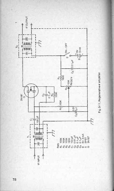
-4 co
rIF
INP
UT
T1 tt
Par
ts
R1
100K
R2
100K
R3
100K
R4
1800
C1
100
pFC
20.
01 µ
FC
30.
1 µF
C4
0.1
p,F
B9V
, 3 m
AS
SP
ST
O3N
187
3N18
7
0.1
µFR
2
100K
R11
00K
0.01
C2,
-',.
/./.F
R4
---N
AA
-18
00
R3,
,,10
0KR
EG
EN
r L
T2
7-7
0 1
ti.F
/ /
Fig
. 3-1
1. R
egen
erat
ive
IF a
mpl
ifier
.
sgO
N-
OF
F
19V
B-=
3 m
A
T_
1
IF O
UT
PU
T

CD
Par
tsR
11M
C3
55 -
300
pF
R2
470K
C4
1000
µFR
33.
3MC
525
R4
47B
12V
, 2 m
AR
522
0L
24-
35 p
.HR
627
00S
SP
ST
3N18
7C
125
µF0
3N18
7C
2 0.
02µF
+ 25 iL
F
INP
UT
1MR
2
R3
1
R6
2700
470K
3.3M
7:-.
7 0.
02 ;I
F
R4
47C
3,-4
55-3
00 p
F
R5
220
C4-
1000
ki.F
C5
+1
25 p
.F
La:2
4-35
µH
II
S \D
N-O
FF
B=
-12V
2 m
A
OU
TP
UT
0
Fig
. 3-1
2. V
ideo
(w
ideb
and)
am
plifi
er.
which general-purpose requirements dictate that both AM and cw signals be received.
Current drain from the 9V source is approximately 3 mA, although this may vary somewhat with individual MOSFETS.
VIDEO (WIDEBAND) AMPLIFIER Video amplifiers are simple -appearing, principally
RC -coupled circuits which exhibit wideband response, operating from low audio frequencies well into the high radio
frequencies. Such amplifiers find a multitude of uses in electronics, but are known principally for their role in TV
picture channels, oscilloscope horizontal and vertical channels, and instrument amplifiers ( especially AC electronic -voltmeter boosters). Figure 3-12 shows the circuit of
a simple MOSFET video amplifier. Frequency response of the circuit extends from 60 Hz to 10
MHz. The input impedance is approximately 1M, determined principally by the resistance of the input resistor R,. Output impedance is approximately 2800f/. These input and output
values hold at 1 kHz. The open -circuit voltage gain of the circuit is approximately 10 at 1 kHz, and is down
approximately 3 dB at 50 Hz and down approximately 6 dB at 10 MHz. The maximum input signal voltage before output peak
clipping is approximately 0.1V RMS, and the corresponding maximum output signal voltage is approximately 1V RMS.
The peaking elements are trimmer capacitor C3 ( 55-300 pF ) and slug -tuned coil L ( 24-35 iuH, Miller 4508 or
equivalent). Both of these components are adjusted carefully for maximum gain of the amplifier at 10 MHz. In a circuit of
this type, successful high -frequency operation demands that all wiring be short, rigid, and direct, and that leads be dressed for optimum high -frequency performance.
In this circuit, MOSFET Q receives its negative gate -1 bias from the voltage drop resulting from the flow of drain current
through source resistors R, and R, in series, and its positive gate -2 bias from voltage divider R2-R3, RF-bypassed by
capacitor C2. With an individual MOSFET, resistance R3 may need some adjustment for maximum gain at 1 kHz. Current
drain from the 12V source is approximately 2 mA, but this may vary somewhat with individual MOSFETS.
80
Chapter 4
Control Circuitsand Devices
The high input resistance, high transconductance, and lowtemperature drift of the MOSFET recommend this type oftransistor for use in control circuits and adjunct devices:sensitive electronic relays, interval timers, alarm devices,automation accessories, and so on. This chapter presents 20such circuits, and these will suggest others to the alertexperimenter.
In each of the circuits, unless indicated otherwise on thecircuit diagram or in the text, capacitances are in picofarads,resistances in ohms, and inductances in henrys. Resistors are1/2W, and electrolytic capacitors are 25V. For simplicity,batteries are shown for DC supply; however, a well filteredpower supply can be used instead of a battery.
Before undertaking the wiring and operation of anycircuit, read carefully the hints and precautions given inChapter 1.
ZERO -CURRENT DC RELAYFigure 4-1 shows the circuit of a sensitive DC relay which
draws so little current (0.15 µA at 1.5V) that, for all practicalpurposes, it may be considered a zero -current device. The DCsignal power required to close the relay is only 0.225µW.
The circuit consists of a single-mosFur DC amplifier with amilliampere -type DC relay connected in a 4 -arm bridge circuitin the drain output section. The bridge allows the static draincurrent of the MOSFET to be balanced out of the relay (byadjustment of potentiometer R3), and its four arms consist ofresistor R2, the two "halves" of potentiometer R3, and theinternal drain -to -source resistance of the MOSFET. The relay isal mA, 1000SZ DC device ( Sigma 5F-1000 or equivalent) .
81

OD
3N18
7
1 5V
INP
UT
Par
ts
R1
10M
R2
1K
R3
1K W
WB
6V, 1
2 m
AK
1 m
A, 1
0000
SS
PS
TQ
3N18
7
/Ii
R2
1K
1 m
A, 1
0000
TO
a --
-O 2
CO
NT
RO
LLE
DC
IRC
UIT
Fk3
BA
LAN
CE
1K W
W
B
6V
Fig
. 4-1
. "Z
ero
-cur
rent
" cc
rel
ay.
0O
N-O
FF
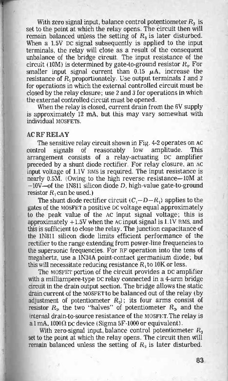
With zero signal input, balance control potentiometer R3 isset to the point at which the relay opens. The circuit then willremain balanced unless the setting of R3 is later disturbed.When a 1.5V DC signal subsequently is applied to the inputterminals, the relay will close as a result of the consequentunbalance of the bridge circuit. The input resistance of thecircuit ( 10M) is determined by gate -to -ground resistor RI. Forsmaller input signal current than 0.15 µA, increase theresistance of R, proportionately. Use output terminals 1 and 3for operations in which the external controlled circuit must beclosed by the relay closure; use 2 and 3 for operations in whichthe external controlled circuit must be opened.
When the relay is closed, current drain from the 6V supplyis approximately 12 mA, but this may vary somewhat withindividual MOSFE1S.
AC RF RELAYThe sensitive relay circuit shown in Fig. 4-2 operates on AC
control signals of reasonably low amplitude. Thisarrangement consists of a relay -actuating DC amplifierpreceded by a shunt diode rectifier. For relay closure, an ACinput voltage of 1.1V RMS is required. The input resistance isnearly 0.5M. (Owing to the high reverse resistance -10M at-10V --of the 1N811 silicon diode D, high -value gate -to -groundresistor R, can be used. )
The shunt diode rectifier circuit ( C, -D -R,) applies to thegates of the MOSFET a positive DC voltage equal approximatelyto the peak value of the AC input signal voltage; this isapproximately +1.5V when the AC input signal is 1.1V RMS, andthis is sufficient to close the relay. The junction capacitance ofthe 1N811 silicon diode limits efficient performance of therectifier to the range extending from power -line frequencies tothe supersonic frequencies. For RF operation into the tens ofmegahertz, use a 1N34A point -contact germanium diode; butthis will necessitate reducing resistance R, to 10K or less.
The MOSFET portion of the circuit provides a DC amplifierwith a milliampere -type DC relay connected in a 4 -arm bridgecircuit in the drain output section. The bridge allows the staticdrain current of the MOSFET to be balanced out of the relay ( byadjustment of potentiometer R3) ; its four arms consist ofresistor R2, the two "halves" of potentiometer R3, and theinternal drain -to -source resistance of the MOSFET. The relay isa 1 mA, 100011 DC device ( Sigma 5F-1000 or equivalent).
With zero -signal input, balance control potentiometer R3set to the point at which the relay opens. The circuit then Willremain balanced unless the setting of R3 is later disturbed.
83
F00
2 µF
AC
INP
UT
(1.1
V R
MS
)
///
DW
1N81
1
Par
ts
R1
470K
R2
1K
R3
1K W
W
C1
0 02
i.LF
B6V
, 12
mA
D1N
811
K1
mA
, 100
051
SS
PS
TQ
3N18
7
R2
Jv\.A
,1K
1 m
A, 1
000S
I
TO
A--
-02
CO
NT
RO
LLE
DC
IRC
UIT
R3
BA
LAN
CE
1K W
W
IN+
0O
N -
OF
F6V
Fig
. 4-2
.A
C-
RF
rel
ay.

When a 1.1V AC or RF signal subsequently is applied to theinput terminals, the relay closes as a result of the consequentunbalancing of the bridge circuit. Use output terminals 1 and 3for operations in which the external controlled circuit must beclosed by the relay closure; use 2 and 3 for operations in whichthe external controlled circuit must be opened.
When the relay is closed, current drain from the 6V supplyis approximately 12 mA, but this may vary somewhat withindividual MOSFETS.
SENSITIVE AF RELAYFigure 4-3 shows the circuit of an audio -frequency AC relay
which operates on an input -signal voltage of 0.1V RMS. Thisarrangement consists of a high -impedance -input AC voltageamplifier Q,, shunt -diode rectifier C3- D - R6, andrelay -actuating DC amplifier Q9. The input AC amplifier has avoltage gain of approximately 10, so that this stage presents asignal voltage of approximately 1V RMS to the diode circuit.The diode circuit, in turn, presents to the DC amplifier apositive voltage equal approximately to the peak value of the1V RMS output of Q,, or approximately +1.4V. This is sufficientto close the relay. The input impedance of the circuit( determined principally by the full resistance of sensitivitycontrol potentiometer 1:11) is 0.5M.
In the AC amplifier stage, MOSFET Q, receives its negativegate -1 bias from the voltage drop resulting from the flow ofdrain current through source resistor R5, and its positivegate -2 bias from voltage divider R2- R3. With an individualMOSFET Q resistance R3 may require some adjustment formaximum voltage gain in the input stage. In the DC amplifierstage, MOSFET Q2 drives a milliampere -type DC relayconnected in a 4 -arm bridge circuit in the drain output section.The bridge allows the static drain current of Q2 to be balancedout of the relay ( by adjustment of potentiometer Rd; its fourarms consist of resistor R7, the two "halves" of potentiometerR, and the internal drain -to -source resistance of MOSFET Q.The relay is a 1 mA, 10005i DC device ( Sigma 5F-1000 orequivalent).
With zero signal input at the input terminals, balancecontrol potentiometer R8 is set to the point at which the relayopens. The circuit then will remain balanced unless the settingof R8 is later disturbed. With potentiometer R, set formaximum sensitivity, when a 0.1V RMS signal subsequently isapplied to the input terminals, the relay closes as the result ofthe consequent unbalancing of the bridge circuit. Use outputterminals 1 and 3 for operations in which the external
85

corn
R3Z
1.5M
R4
1800
3N18
73N
187
02
AF
INP
UT
817
0 5M
0.1V
RM
SO
I
R2
470K
R5
270
2 -^
,50
µF
DW
1N81
1R
647
0K
Par
ts
R1
0.5M
R2
470K
R3
1.5M
R4
1800
R5
270
R6
470K
R7
1K
R8
1K W
W
Ci
0 1
µFC
250
µF
C3
0.02
µFB
6V, 1
5 m
AD
1N81
1K
1 m
A, 1
0000
SS
PS
T01
3N18
702
3N18
7
1 m
A, 1
0000
0 2 3
TO
CO
NT
RO
LLE
D
RB
ALA
NC
EC
IRC
UIT
1K W
W
SE
NS
ITIV
ITY
Fig
. 4-3
. Sen
sitiv
e A
F r
elay
.
III 6V15
mA
S
ON
-O
FF
controlled circuit must be closed by the relay closure; use 2and 3 for operations in which the external controlled circuitmust be opened.
When the relay is closed, current drain from the supply isapproximately 15 mA, but this may vary somewhat withindividual MOSFE'M
LC -TUNED AF RELAYRelay operation often is desired at a single frequency. In
Fig. 4-4, single -frequency operation is achieved by tuning theAC amplifier stage of a circuit which is substantially the samein other particulars as the one described in the precedingsection. Tuning is accomplished with parallel -resonant circuitL-C2 in the drain circuit of MOSFET Q,. The AC output of thetuned amplifier is rectified by the shunt diode circuitC5-D-R5, and the resulting DC voltage is applied to DCamplifier Q2, which, in turn, actuates milliampere -type DCrelay K.
Inductor L and capacitor C2 must be chosen for the desiredfrequency Jr Generally, the inductor will govern thecaacitance, since few inductors for AF use can be varied. Witha given inductance L, the required capacitance C2 which canbe built up accurately can be determined with the aid of thefollowing equation, in which L is in henrys, C2 in farads, and frin hertz:
C2 =39.512L (Eq. 4-1)
From this equation, it is seen that for an available 10Hinductor, the required capacitance C2 for resonance at 1000 Hzis 0.0025µF.
The input AC amplifier Q, has a voltage gain ofapproximately 10, so that this stage presents an amplifiedsignal voltage of 1V RMS to the diode circuit when the inputsignal voltage at the input terminals is 0.1V RMS. The diodecircuit, in turn, presents to the DC amplifier Q2 a positivevoltage equal approximately to the peak value of the 1V RMSoutput of Q1, or approximately +1.4V. This is sufficient to closerelay K.
In the DC amplifier stage, MOSFET Q2 drives amilliampere -type DC relay in a 4 -arm bridge circuit in thedrain output section. The bridge allows the static drain currentof Q2 to be balanced out of the relay (by adjustment ofpotentiometer R6), and its four arms are resistor R7, the two"halves" of potentiometer R6, and the internal drain -to -sourceresistance of MOSFET Q2. The relay is a 1 mA, 100051 DC device(Sigma 5F-1000 or equivalent) .
87

OD op
3N18
7Qi
0.02
µF
Ci
L
1 'IF
Par
ts
R1
0.5M
C3
50µF
R2
470K
04 1
0 p.
F
r0i
R3
1.5M
05 0
.02µ
FR
4 27
0B
6V, 1
5 m
AR
5 47
0KD
1N81
1A
D
R6
1KW
WL
SE
E1N
811
R7
1KT
EX
TC
10.
1 µF
K1
mA
,A
F IN
PU
TR
1R
3C
2 S
EE
TE
XT
1000
00.
5MS
SP
ST
PO
T1.
5MO
t 3N
187
G2
3N18
7
R2
470K
R4
270G
I oF C
4+
10p.
F
R5
470K
C_)
R7
,\AA
,1K
1 m
A, 1
0000
R6
v B
ALA
NC
E
23 TO
CO
NT
RO
LLE
DC
IRC
UIT
1KW
W
SE
NS
ITIV
ITY
//
Fig
. 4-4
. LC
-tu
ned
AF
rel
ay.
s
6V15
mA
ON
-O
FF

With zero -signal input, balance control potentiometer R6 is
set to the point at which the relay opens. The circuit then willremain balanced unless the setting of R6 is later disturbed.When a 0.1V AC signal at the frequency determined by L and C2then is applied to the input terminals (with potentiometer R,
set for maximum sensitivity), the relay closes as a result ofthe consequent unbalancing of the bridge circuit. Use outputterminals 1 and 3 for operations in which the externalcontrolled circuit must be closed by the relay closure; use 2and 3 for operations in which the external controlled circuitmust be opened.
When the relay is closed, current drain from the 6V supply
is approximately 15 mA, but this may vary somewhat withindividual MOSFETS.
RC -TUNED AF RELAYThe tuned audio -frequency relay circuit shown in Fig. 4-5
performs in the same manner as the LC -tuned circuitdescribed in the preceding section. The RC -tuned circuit,however, needs no inductor, but achieves audio -frequencytuning by means of a parallel -T network(C2-C3-C4-R6-R7-R8) in the input stage of the circuit. In allother respects, the circuit is similar to the one shown earlier inFig. 4-4. Resistance-capacitance tuning is of value wheniron -core inductors are to be avoided and when continuouslyvariable tuning is desired.
In this circuit, tuning to a peak is accomplished byincorporating a null circuit (the parallel -T network) in thenegative feedback loop between the drain output and gate -1input section of the first stage ( Q,) . The result of this is thatnegative feedback occurs at all frequencies except the nullfrequency of the network ( null frequency Jr = 1/6.28R,C2 inFig. 4-5), which is removed by the network, canceling the gainat those frequencies. But the amplifier has full gain atfrequency f,, since this one frequency is not included in thefeedback. The net result is tuned bandpass-peak response.
In the RC network, C2 = C3 = 0.5C4, and R6 = R, = 2R8.
When these relationships are preserved, the null frequency iscalculated as
1Jr -
6.28R6C2 (Eq. 4-2)
where fr is in hertz, R6 in ohms, and C2 in farads.From Eq. 4-2, it is seen that for a parallel -T network in
which C2 and C3 are each 0.1 AF, C4 = 2C3 = 0.2 f.LF, R6 and R,
are each 15920, and R8 = 0.5R6 = 7960, the null frequency is
89

CiD
3N18
701 R
4
Par
ts
R1
10K
R8
SE
E T
EX
T C
43 S
EE
TE
XT
D1N
811
R2
1MR
918
00C
4 S
EE
TE
XT
K1
mA
, 100
0f2
R3
470K
R10
470
KC
5 50
µFS
SP
ST
R4
1.5M
R11
1K
C6
10µF
3N18
7
R5
270
R12
1K
WW
07 1
0µF
02 3
N18
7F
I8 S
EE
TE
XT
C1
0.1
µFC
8 0.
02µF
R7
SE
E T
EX
T C
2 S
EE
TE
XT
B 6
V, 1
5 m
A3N
187
0.02
µF
.
=R
loD
1N
811
02
470K
C j1
mA
,100
012
1T
O
-02
CO
N-
TR
OLL
ED
3 C
IRC
UIT
R12
, BA
LAN
CE
1K W
W
1 5M
470K
R5
///S
EN
SIT
IVIT
Y
1+27
0 C
5" 5
0 /IF
C8
10µF
T
Fig
. 4-5
. RC
-tu
ned
AF
rel
ay.
B
III
SP
ST
ON
-O
FF
ev15
mA

1000 Hz (the peak frequency frof the amplifier). In general, itis best to select the three capacitances (C2 = C3 = 0.5C4) andthen to adjust the resistances to exact values ( R6 = R, = 2R8)as required. The following equations-in which resistances arein ohms, capacitances are in farads, and peak frequency is inhertz-will help:
R6 = R7 -6.281,C2
(Eq. 4-3)
R8 = 0.5R6 (Eq. 4-4)
The resistances and capacitances must have exact values.The sharpness of tuning will depend upon the closeness withwhich these components meet specified values. The circuitmay be made continuously tunable by using a 3 -gangpotentiometer for R6 -R7 -R8 and switching the capacitors ingroups of three to change frequency ranges. In this way, theamplifier can be given tuning ranges of 20-200 Hz, 200-2000Hz, and 2-20 kHz, to cover the audio -frequency spectrum.
Input AC amplifier Q1 has a voltage gain of approximately10, so that this stage presents an amplified signal voltage of 1VRMS to the diode circuit C8 -D -R10 when the signal voltage atthe input terminals is 0.1V RMS and potentiometer R2 is set formaximum sensitivity. The diode circuit, in turn, rectifies thisvoltage and presents a resulting DC voltage to DC amplifier Q2.This latter voltage is approximately +1.4V, which is the peakvalue of the 1V RMS output of the first stage. This is sufficientto close the relay.
In the DC amplifier stage, MOSFET Q2 drives amilliampere -type DC relay in a 4 -arm bridge circuit in thedrain output section. The bridge allows the static drain currentof Q2 to be balanced out of the relay ( by adjustment ofpotentiometer R12), and its four arms consist of resistor R,,,the two "halves" of potentiometer Ri, and the internaldrain -to -source resistance of MOSFET Q2. The relay is a 1 mA,100051 device (Sigma 5F-1000 or equivalent).
When the relay is closed, current drain from the 6V supplyis approximately 15 mA, but this may vary somewhat withindividual MOSFETS.
COINCIDENCE RELAYA relay that closes when two signals arrive at the same
instant ( or when they overlap for a part of their duration) isuseful in various counting, sampling, and automatic controlsystems. Figure 4-6 shows a coincidence relay of this type,employing a single MOSFET. A MOSFET in this applicationpresents high resistance (low loading) to both signal sources.
91

cr)
Par
ts
R1
1M
R2
1 M
R3
1K
Ft4
1K W
WB
12V
, 24
mA
K2
mA
, 250
00S
SP
ST
O3N
187
3N18
7O
INP
UT
10
INP
UT
20
CO
MM
ON
01M
R2
1M
R3
NA
A.,
1K
r--3 A--3
0
2 3
R"
BA
LAN
CE
1K W
W
2 m
A, 2
5000
1
TO
CO
NT
RO
LLE
DC
IRC
UIT
12V
24
mA
Fig
. 4-6
. Coi
ncid
ence
rel
ay.
0O
N O
FF

Each input signal has a voltage of +1.5V. Signal 1 isapplied to gate 2 of the MOSFET, and signal 2 is applied to gate1. When either one of these signals is applied alone, thedrain -current increase that it produces is insufficient to closethe relay. When both signals are applied at the same time,however, the increase in drain current will do so.
The circuit is essentially that of a DC amplifier. The relayoperates in a 4 -arm bridge in the drain circuit. The bridgeallows the static drain current to be balanced out of the relay( by adjustment of potentiometer R4) ; its four arms consist ofresistor R3, the two "halves" of potentiometer R4, and theinternal drain -to -source resistance of MOSFET Q. The relay is a2 mA, 25000 device (Sigma 5F-2500 or equivalent). With zerosignal at input 1 and input 2, balance control potentiometer R4is set to the point at which the relay opens. The circuit then willremain balanced unless the setting of R4 is later disturbed. Useoutput terminals 1 and 3 for operations in which the externalcontrolled circuit must be closed by the relay closure; use 2and 3 for operations in which the external controlled circuitmust be opened.
When the relay is closed, current drain from the 12Vsupply is approximately 24 mA, but this may vary somewhatwith individual mosFETs.
SENSITIVE PHOTOELECTRIC RELAYThe output of a conventional selenium self -generating
photocell ( typically 0.3V DC, 77 /IA, at 100 footcandles ) is toolow to operate a DC relay directly. The circuit given in Fig. 4-7provides a simple DC amplifier for boosting the output of sucha photocell. -In this circuit, the DC output of photocell PC isapplied directly to the MOSFET ( positive output to the gatesconnected in parallel, and negative output to the sourceelectrode), and a milliampere -type DC relay is operated in a4 -arm bridge in the drain circuit.
The bridge-consisting of resistor R2, the two "halves" ofpotentiometer RI, and the internal drain -to -source resistanceof the mosFET-allows the static drain current to be balancedout of the relay ( by adjustment of potentiometer R,) . Therelay, K, is a 1 mA, 10000 device ( Sigma 5F-1000 orequivalent) .
With the photocell darkened, balance controlpotentiometer R, is set to the point at which the relay opens.The circuit then will remain balanced unless the setting of R, islater disturbed. When the photocell subsequently isilluminated, the relay will close. Use output terminals 1 and 3'for operations in which the external controlled circuit must be
93

ct)
Par
ts
R1
R2
B K PC
S
R2
1K W
W1K
1K6V
, 12
mA
K1
mA
, 100
00S
ELE
NIU
M P
HO
TO
CE
LLS
PS
T3N
187
1 m
A. 1
0005
2O
3N18
7 PC
A-0
2C
IRC
UIT
PO
S
Rte
BA
LAN
CE
NE
G
TO
CO
NT
RO
LLE
D
1K W
W
B
III+
ON
-OF
F6V
Fig
. 4-7
. Sen
sitiv
e ph
otoe
lect
ric r
elay
.

closed by the relay closure; use 2 and 3 for operations in whichthe external controlled circuit must be opened.
When the relay is closed, current drain from the 6V supplyis approximately 12 mA, but this may vary somewhat withindividual MOSFETs.
TEMPERATURE -SENSITIVE RELAYFigure 4-8 shows the circuit of an electronic
temperature -sensitive relay. In this arrangement, athermistor ( thermally sensitive resistor) R, is operated fromthe 6V DC supply along with a simple DC amplifier based on theMOSFET Q. The DC output of the thermistor is applied to theMOSFET to close the relay.
The thermistor and potentiometer R2 form a voltagedivider which allows close selection of thetemperature -dependent voltage applied to the gates. As thetemperature rises, the resistance of the thermistor decreasesproportionately, allowing the thermistor current to increaseand the output of potentiometer R2 ( and accordingly the gatevoltage) to increase. Potentiometer R2 is adjusted to the pointat which the gate voltage at the desired temperature issufficient to close the relay.
Relay K operates in a 4 -arm bridge-consisting of resistorR4, the two "halves" of potentiometer R3, and the internaldrain -to -source resistance of the MOSFET-in the drain circuit.This bridge allows the static drain current to be' balanced outof the relay ( by adjustment of potentiometer R3) . The relay isa 1 mA, 100011 device ( Sigma 5F-1000 or equivalent) .
With the thermistor temporarily disconnected, balancecontrol potentiometer R3 is set to the point at which the relayopens. The circuit then will remain balanced unless the settingof R3 later is disturbed. The thermistor may be a FenwalGB42JM1 device, or the equivalent.
When the relay is closed, current drain from the 6V supplyis approximately 14 mA.
TOUCH -PLATE RELAYFigure 4-9 shows the circuit of a simple electronic relay
that responds to a light touch of the finger. Such touch -platerelays have become common for operating all sorts ofelectrical equipment. In this arrangement, gate 1 of theMOSFET is grounded, and gate 2 is allowed to float and isconnected to the pickup, which is a small disc of sheet metal orfoil. The floating gate is highly susceptible to pickup, so thatmerely touching the finger to it couples in enough stray pickupenergy to drive the MOSFET.
95
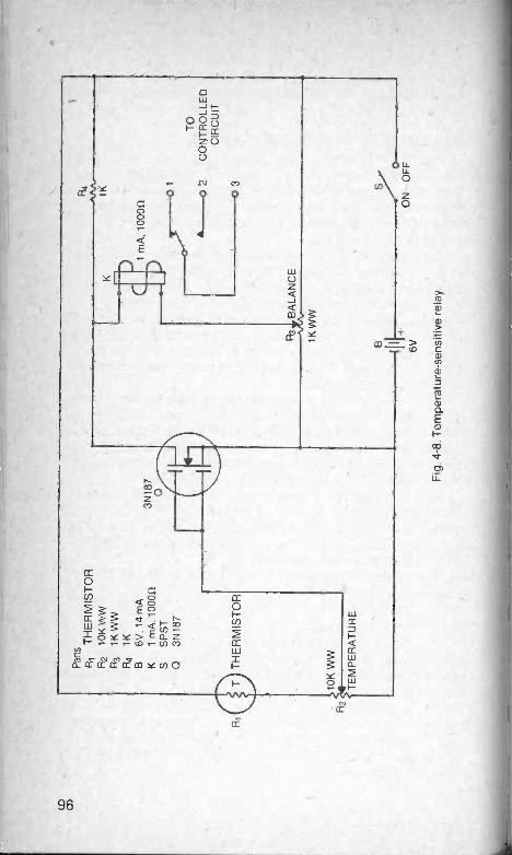
Par
ts
R1
TH
ER
MIS
TO
RR
210
K W
WR
31K
WW
R4
1KB
6V, 14 mA
K1 mA, 10000
SS
PS
TQ
3N18
7
TH
ER
MIS
TO
R
10K
WW
R2
TEMPERATURE
3N18
7
R4
AA
A,
1K
1 mA, 10000
R3
BALANCE
NX
A,
1K W
W
TO
2CONTROLLED
CIR
CU
IT
6V
Fig
. 4-8
. Tem
pera
ture
-se
nsiti
ve r
elay
.
OON-OFF

ME
TA
L P
LAT
E O
R D
ISC
3N18
7O
Par
ts
R1
1K
R2
1K W
WB
12V
, 16
mA
K1
mA
. 100
00S
SP
ST
O3N
187
1 m
A, 1
0000
02
R2v
Tiv
BA
LAN
CE
1K W
W
/ //
c0
Ri
NA
A,
1K
TO
CO
NT
RO
LLE
DC
IRC
UIT
1111
+0
12V
ON
- O
FF
Fig
. 4-9
. Tou
ch -
plat
e re
lay.
The MOSFET serves as a simple DC amplifier with a milliampere -type DC relay in its drain circuit. The relay is
connected in a 4 -arm bridge circuit-consisting of resistor R,, the two "halves" of potentiometer R2, and the internal
drain -to -source resistance of the mosFET-which allows the static drain current of the MOSFET to be balanced out of the relay ( by adjustment of R2). The relay is a 1 mA, 1000f1 device
( Sigma 5F-1000 or equivalent). With the pickup plate protected from any nearby bodies, balance control potentiometer R2 is set to the point at which
the relay opens. The circuit then will remain balanced unless the setting of R2 is later disturbed. When the pickup plate
subsequently is touched, the relay will close. Use output terminals 1 and 3 for operations in which the external controlled circuit must be closed by the relay closure; use 2
and 3 for operations in which the external controlled circuit must be opened.
When the relay is closed, current drain from the 12V supply is approximately 16 mA, but this may vary somewhat
with individual MOSFETS.
CAPACITANCE RELAY Capacitance relays, also called instrusion relays, are
familiar in many areas of electronics, as well as in nonelectronic applications. They are often found in burglar
alarms and other anti -intrusion devices. Figure 4-10 shows the circuit of a capacitance relay employing a MOSFET in the sensitive radio -frequency stage and
a silicon bipolar transistor in the high -gain DC amplifier stage. In this arrangement, MOSFET Q, operates at a high radio
frequency in conjunction with inductor L, trimmer capacitor C2, and radio -frequency choke RFC. ( All three of these
components are self-contained in a commercial unit T, such as Miller 695.) The MOSFET stage oscillates lightly; and when a
hand or other part of the human body comes near the pickup antenna ( a short piece of wire with or without a metal disc or
plate on its end), the MOSFET drain current undergoes a small change. This change is coupled to the base input of the 2N2712
DC amplifier which, in turn, closes the relay. To set up the circuit initially, protect the pickup antenna
from any nearby bodies, including the operator's. Then work back and forth between adjustments of threshold control R5 and sensitivity control R3 until relay K closes. Next, back off the setting of R5 until the relay just opens. Then bring the hand
close to the antenna and adjust trimmer C2 and sensitivity control R3 until the relay closes. Withdrawing the hand should
98

TW
-rj1
.11-
...
CD
'PIC
KU
PA
NT
EN
NA
ci
T0
1
T (
SE
E T
EX
T)
601_
,I
c 2R
FC
I"-
4
L Ri
10M
3N18
7Q
i
C3-
0.00
2R
282
0
Par
ts
R1
10M
R2
820
R3
5KW
WR
42.
2KR
520
0 W
WC
i0.
1 i..
(FC
2 S
EE
TE
XT
C3
0.00
2C
40.
01 A
LF
2N27
12B
9V, 1
5 m
A
02K
1 m
A, 1
0005
1
R5,
4200
WW
SS
PS
TT
SE
E T
EX
TT
HR
ES
HO
LDQ
i3N
187
K02
2N27
12
R34
A,
5KW
W2.
2KS
EN
SIT
IVIT
YC
a
T0.
01µF
1111
+9V
SP
ST
ION
-OF
F
Fig
. 4-1
0. C
apac
itanc
e re
lay.
1 m
A, 1
0000
2T
OC
ON
TR
OLL
ED
CIR
CU
IT

then cause the relay to open. When the circuit is correctly adjusted, bringing the hand to the desired distance from the antenna should close the relay, and withdrawing the hand
should open it. The circuit must not be so adjusted that it will self -operate intermittently.
The relay is a 1 mA, 10000 device ( Sigma 5F-1000 or equivalent). When the relay is closed, current drain from the
9V supply is approximately 15 mA, but this may vary somewhat with an individual 3N187 and 2N2712.
SOUND SWITCH The circuit shown in Fig. 4-11 closes a relay when it "hears" a sound of the proper intensity. In this arrangement,
the MOSFET acts as an AC voltage amplifier, diode D as a signal rectifier, and silicon bipolar transistor Q2 as a DC amplifier
driving relay K. A small crystal microphone (MIC) picks up the sound and delivers a proportionate AC voltage to gate 1 of the MOSFET through sensitivity control potentiometer RI.
The MOSFET delivers an amplified sound voltage to the shunt rectifier circuit (C3, D, and the internal base -to -emitter path of transistor Q2) which, in turn, delivers the resulting DC
voltage to the base of Q2. The latter transistor then amplifies the DC and closes relay K. The diode must be poled as shown in
Fig. 4-11, so that a positive DC voltage is applied to the Q2 base. The relay operates directly in the collector circuit of the 2N2712. Since the static current IC° of the 2N2712 is so low, it cannot affect the relay, so no balancing circuit is needed. The
relay is a 1 mA, 10000 device ( Sigma 5F-1000 or equivalent). Use output contacts 1 and 3 for operations in which the
external circuit must be closed by the relay closure; use 2 and 3 for operations in which the external controlled circuit must
be opened. Initially, set sensitivity control R, for maximum
sensitivity. Then, with the microphone picking up the desired level of noise, adjust R5 so that the relay just closes. Louder
intensities then may be accommodated by turning down the adjustment of RI.
When the relay is closed, current drain from the 12V supply is approximately 17 mA, but this may vary somewhat
with an individual 3N187 and 2N2712.
INTERVAL TIMER Figure 4-12 shows the circuit of a conventional interval
timer in which the very high input resistance of the MOSFET affords performance comparable to that of the usual
vacuum -tube model. Because of the smallness of the MOSFET,
100

MIC
0.1
µF
CR
YS
TA
LM
ICR
O-
PH
ON
E
/1
Ri
R4Z
470
K
R5
0 5M
LEV
EL
AD
JUS
T
3N18
701
R6
1800
1M SE
NS
ITIV
ITY
R2
470K
2N27
12
C3
0.1
/..).
F
D1N
811
IT
R3
270
C2
50µF
Fig
. 4-1
1. S
ound
sw
itch.
1 m
A, 1
0001
)
a--0
23
Par
tsR
i1M
TO
R2
470K
CO
NT
RO
LLE
DR
327
0C
R4
470K
R5
0.5M
R6
1800
GI
0.1
tiFC
2 50
µFC
30.
1 /J
.FB
12V
, 17
mA
D1N
811
K1
mA
, 100
011
SS
PS
T3N
187
Q2
2N27
12
12V
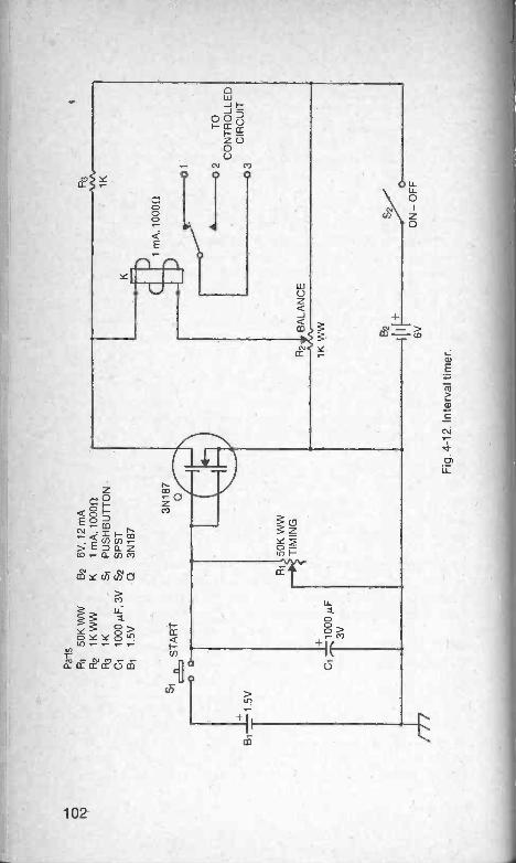
1 5V
Par
ts
R1
50K
WW
B2
6V, 1
2 m
AR
21K
WW
K1
mA
, 100
0(2
R3
1KS
iP
US
HB
UT
TO
NC
i10
00µF
, 3V
S2
SP
ST
Bi
1.5V
O3N
187
f,S
TA
RT
3N18
7O
Ci
1000
µF3V
R1
50K
WW
--0.
1 T
IMIN
G
1 m
A. 1
0000
R2v
7A13
ALA
NC
E1K
WW
/ / /
Fig
. 4-1
2. In
terv
al ti
mer
.
B2
1111
+6V
2T
OC
ON
TR
OLL
ED
ti
3C
IRC
UIT
OO
N-O
FF

relay. 1000 µF ( 3V) capacitor, and other components, theentire unit can be very small and compact.
In this arrangement, the 3N187 MOSFET serves as a simpleDC amplifier driving relay K in its drain circuit. Whenpushbutton switch S, is depressed momentarily, capacitor C, ischarged from 1.5V cell B,. At the same time, relay K is closed.When S, then is released, capacitor C, discharges at a ratedetermined by resistance R, and capacitance C, ( the timeinterval before the relay drops out is closely equal to the timeconstant of the circuit: t = RC seconds). The time instant thatthe relay drops out may be controlled by proper setting oftiming control rheostat R,. With the 50,00051 control and 1000/IF capacitor shown, the maximum time interval is 50 sec.Other maximum values may be obtained by appropriateselection of C, and R, values in accordance with thetime -constant formula.
The relay is a 1 mA, 100052 device ( Sigma 5F-1000 orequivalent) operated in a 4 -arm bridge in the drain circuit. Thebridge-consisting of resistor R3, the two "halves" of balancecontrol potentiometer R2, and the internal drain -to -sourceresistance of the mosFur-allows the static drain current to bebalanced out of the relay (by adjustment of potentiometer R2)before attempting to operate the timer.
When the relay is closed, current drain from the 6V supplyB2 is approximately 12 mA, but this may vary somewhat withindividual MOSFETS. The 1.5V cell, B1, is used onlyintermittently, supplying charging current to capacitor CI, andshould enjoy long life, especially if a size D celrls used.
Vg
CONTINUOUSLY VARIABLE PHASE SHIFTERFigure 4-13 shows the circuit of a device which will give
smooth variation of phase between input and output ofapproximately zero to 180° by adjusting a single control (R6).The circuit is basically that of a common -source amplifierwith unbypassed source resistor ( R4).
When R6 is adjusted to full resistance, it offers minimumloading of the MOSFET, and the output signal is effectivelytaken from the drain electrode and is 180° out of phase with theinput signal. When instead, R6 is adjusted to zero(potentiometer minimum), the output signal is effectivelytaken from the source electrode, somewhat in the manner of asource follower, and the output is of the same phase ( 0°) as theinput. Between these two limits, a smooth variation of phase isobtained. Capacitor C3 for output coupling must be chosen, -with respect to the external load, such that it does not
103
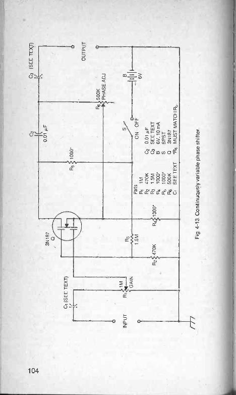
C2
Ca
(SE
E T
EX
T)
INP
UT
CI (
SE
ET
EX
T)
1M GA
IN
3N18
7O
R5
1000
"
IC0.
01 A
F
1:11
500K
PH
AS
E A
DJ
Ri
R3
.
1 5M
Par
tsO
N-O
FF
Ri
1M6V
R2
470K
020.
01 p
_F
R2
470K
R4
1000
'R
31.
5MC
GS
EE
TE
XT
R4
1000
*B
6V, 1
0 m
AR
510
00*
SS
PS
TR
650
0K0
3N18
7C
iS
EE
TE
XT
*R4
MU
ST
MA
TC
H R
5
/F
ig. 4
-13.
Con
tinuo
usly
var
iabl
e ph
ase
shift
er.
I
OU
TP
UT
0

introduce additional undesired phase shift. This applies also toinput capacitor CI.
Voltage gain of the circuit is approximately 3.5. Themaximum input signal voltage before peak clipping is 0.6VHMS: the corresponding output signal voltage is 2.1V RMS. Inthis circuit, gate 1 of the MOSFET receives its negative biasfrom the voltage drop resulting from the flow of drain currentthrough source resistor R4, and gate 2 receives its positive biasfrom voltage divider R2- R3. With an individual MOSFET,resistance R, may need some adjustment for maximum gain.
Current drain from the 6V source is approximately 10 mA,but this may vary somewhat with individual MOSFETS.
STEP -TYPE PHASE SHIFTERThe circuit shown in Fig. 4-14 is of the same type as the
variable phase shifter described in the preceding section andshown in Fig. 4-13, except that here the phase is varied in stepsby means of phase selector switch S2, instead of beingcontinuously variable. This difference will suit manyapplications calling for discrete steps of phase. A commoncapacitor (C2, 0.01 µF) is employed for all phase steps. It isonly necessary, then, to preset each of the potentiometers ( R6,R,, R8...Rn) for the desired phase shift, with the aid of anoscilloscope set up for Lissajous patterns. Each potentiometercan be 500,00011 maximum.
The general particulars of operation of the circuit are thesame as those given for the variable phase shifter in theprevious section.
SENSITIVE CARRIER -FAILURE ALARMA carrier -failure alarm is a useful monitor at radio
stations of all kinds that remain on the air for extendedperiods. When amplification is employed in a device of thistype, very little RF pickup is required, and no connection to thetransmitter is necessary. Figure 4-15 shows a carrier -failurecircuit embodying a diode detector and MOSFET DC amplifier.The latter operates a relay which actuates the alarm deviceitself.
A simple diode detector circuit is employed. This consistsof tuned circuit L-C,, 1N34A germanium diode D, loadresistor RI, bypass capacitor C2, radio -frequency choke RFC,and bypass capacitor C3. Capacitance C, and inductance L areselected to resonate at the frequency of the monitored carrier.Table 4-1 gives coil -winding instructions for coils to cover thefrequency range 440 kHz to 30 MHz when C, is a 365 pF variable -capacitor. For ham bands, use a 100 or 50 pF capacitor and
105

3) a)
C1
(SE
E T
EX
T)
INP
UT
Ri
1M 4 GA
INR
3
1.5M
R5
C2
1000
'
C3
(SE
E T
EX
T)
Rns
:
(19n
:1;
0S
2 P
HA
SE
SE
LEC
TO
R
R2
470K
R41
000'
0P
arts
ON
-O
FF
R1
,1M
C2
0.01
µFR
247
0KC
3 S
EE
TE
XT
R3
1.5M
B6V
, 10
mA
R4
1000
'S
1S
PS
TR
510
00*
S2
SE
E T
EX
TR
6, R
7, R
g, R
n E
AC
H 5
00K
Ci
SE
E T
EX
T0
3N18
7'R
4 M
US
T M
AT
CH
R5
OU
TP
UT
(E
o)
0
III
Fig
. 4-1
4. S
tep
-typ
e ph
ase
shift
er.

PIC
KU
P A
NT
EN
NA
L o
Ci
TU
NIN
G
R1
2.7K
C2
Par
ts
R1
2.7K
R2
1KW
WR
31K
C2
0 00
2 p.
FC
30.
002µ
FB
6V, 1
2 m
AD
1N34
AR
FC
2.5
mH
K1
mA
, 100
00S
SP
ST
Q3N
187
OS
EE
TE
XT
FO
R L
AN
D C
i
R3
1K
1 m
A. 1
0000
a---
-0 2
R2
IF B
ALA
NC
EMh
1K W
W
Fig
. 4-1
5. S
ensi
tive
carr
ier
-fai
lure
ala
rm.
3 TO
CO
NT
RO
LLE
DC
IRC
UIT
B
1111
+6V
ON
-O
FF

Table 4-1. Coil Data for Sensitive Carrier -Failure Alarm.*
Coil A 440-1200 kHz 187 turns No. 32 enameled wire closewound
Coil B on 1 in diameter form. 1-3.5 MHZ 65 turns No. 32 enameled wire closewound on
Coil C 1/2 in. diameter form. 3.4-9 MHz 27 turns No. 26 enameled wire closewound on
Coil D 1/2 in diameter form. 8-20 MHz 10 turns No. 22 enameled wire on V2 in. diameter
Coil E form. Space to winding length of 1/2 in. 18-30 MHz 5V2 turns No. 22 enameled wire on ,/2 in. diameter
form. Space to winding length of 1/2 in.
'(based on tuning capacitor Ci = 365 pF variable.)
standard, manufactured, transmitter -type coils to go with the chosen capacitance, when the wide coverage provided by Table 4-1 is not desired. The signal is picked up by a small
antenna, which can be a standard vertical whip or a short section of stiff vertical wire.
When a signal is tuned in, diode D delivers a positive Pc voltage to the gates of the MOSFET Q. The MOSFET amplifies the
DC and drives the relay. The relay is a 1 mA, 100011 device ( Sigma 5F-1000 or equivalent) operated in a 4 -arm bridge
circuit in the drain section. The bridge-consisting of resistor R3, the two "halves" of balance -control potentiometer R2, and the internal drain -to -source resistance of the mosFET-allows the static drain current to be balanced out of the relay (by
adjustment of potentiometer R2) before attempting to operate the instrument.
When the relay is closed, current drain from the 6V supply is approximately 12 mA, but this may vary somewhat with
individual MOSFETS. Use output terminals 1 and 3 when the circuit of the external alarm device must be closed by the
relay actuation (example, a lamp or bell that is switched on) ; use 2 and 3 when the external circuit must be open 3d
( example, a lamp that is to be switched off).
LOGIC AND CIRCUIT Figure 4-16 shows a 2 -stage AND circuit which performs the
logic AND operation in control or counting circuits. The use of MOSFETS in this arrangement provides high input resistance
and accordingly low drain on the switching source. The arrangement is essentially that of two DC amplifiers having a
common source resistor, R5. Output is taken from across this resistor. The gates of each MOSFET receive a -1.5V switching
signal. Normally, output E, = +2V. If either one of the gates receives its signal, but the other gate does not, E, is reduced
108

CO
MM
ON
+
R1
1nA
.47
0K
3N 1
87
Q1
4.7M
I
4-\
0O
N-O
FF
16V
B-
B2
mA
R2
4.7M
/P
arts
R1
470K
R3
470K
R4
4.7M
R5
1KB
6V. 2
mA
SS
PS
TQ
t3N
187
Q2
3N18
7
R52
1KO
UT
PU
T
/-7-
7
O (.13
Fig
. 4-1
6. L
ogic
AN
D c
ircui
t.

slightly because of reduced drain current flowing through R5. If both gates receive their -1.5V signals at the same time,
however ( that is, E, and E2 are present), Eo is reduced to zero. When the circuit is performing the AND function, current
drain from the 6V supply is approximately 2 mA, but this may vary somewhat with individual mosFors.
LOGIC OR CIRCUIT Figure 4-17 shows a single -stage OR circuit which
performs the logic OR operation in control or counting circuits. The use of a MOSFET in this arrangement provides high input
resistance and accordingly low drain on the switching -signal source. The arrangement is essentially a dual -input, single -stage DC amplifier.
Each gate of the MOSFET receives a +1.5V switching signal. Initially, output voltage E, = IV. If either E, or E2 is
applied, however, E, drops to 0.25V. Thus, either one of the input signals will perform the operation (E, or E2 will switch
the circuit)
DC SIGNAL INVERTER In some control or counting circuits, a DC signal or trigger must be changed in polarity as well as amplified. Figure 4-18
shows one type of circuit for accomplishing this. This is seen to be a simple DC amplifier with a conventional bucking section
(B2 -S2-1?,) in its output. Use of a MOSFET in this arrangement provides high input impedance and accordingly negligible
loading of the switching -signal source. When the input switching signal is applied, the gates of the
MOSFET become positive with respect to the source. This causes an increase in drain current, which reduces the drain
voltage. Initially, however, the static output voltage has been balanced out by adjustment of potentiometer R3; so the output
voltage actually increases, but in the negative direction. Initially, the circuit is balanced (with zero input signal) by
adjusting balance control potentiometer R3 for zero voltage at the output terminals. The circuit then will remain balanced
unless the setting of R3 is later disturbed. When a +1.5V signal subsequently is applied to the input terminals, the voltage at
the output terminals becomes approximately -2.8V. Thus, the input voltage has been inverted and, at the same time, has been amplified 1.87 times.
When the circuit is in full operation, current drain from battery B, is approximately 10 mA, and that from battery B2 is
approximately 1.2 mA. The currents may be somewhat different from these values with individual mosFETs.
110

Eim
i +1.
5V
Ein
2 +
1.5V
CO
MM
ON
-o
Flt
470K R2
470K
Par
ts
Ri
R2
470K
470K
ON
-OF
FbV
R3
4.7M
B.=
2 m
A
R4
4.7M
R5
B2.
2K6V
, 2 m
A
R52
2.2K
/S
SP
ST
O3N
187
3N18
7
R3
4.7M
R4
4.7M
O
0+
OU
TP
UT
0 -
Fig
. 4-1
7. L
ogic
OR
circ
uit.

3N18
7
+0
INP
UT
(0-
1.5V
)R
i
-o
470K
-10
M
R2
500 O
N-O
FF
Si
S2
I 6VB
i - T10
mA
R3
BA
LAN
CE
5K W
WP
arts
R1
470K
-10
MB
250
0R
3 5K
WW
Bi
6V, 1
0 m
AB
26V
,1.2
mA
B1,
2 D
PS
TQ
3N18
7
B2
6V1.
2 m
A
OU
TP
UT
(0-2
.8V
)
i+
Fig
. 4-1
8. D
c si
gnal
inve
rter
.

DC IMPEDANCE CONVERTERFigure 4-19 shows the circuit of a device that presents a
high resistance to a DC source and a low resistance to a load.This is essentially a DC source follower, and it is useful in allcontrol and instrumentation applications in which as much aspossible of a DC voltage must be transmitted from ahigh -resistance source to a low -resistance load. The inputresistance is determined chiefly by the full resistance ofsensitivity control potentiometer R1; however, beyond 5M orso. problems may be encountered with stray pickup. Theoutput resistance is closely that of the the source resistor( here. 500f/1.
Initially, a static DC voltage appears at the output that isthe result of the voltage drop produced by drain currentthrough source resistor R2. But this voltage is balanced out byadjustment of potentiometer R3. The circuit then remainsbalanced unless the setting of this potentiometer is laterdisturbed. When a +1.5V signal subsequently is presented tothe input terminals, with R, set for maximum sensitivity, thevoltage at output terminals swings to +0.9V.
When the circuit is in full operation, current drain frombattery B1 is approximately 0.45 mA, and that from battery B2is approximately 2.6 mA. The output load device should nothave a resistance lower than 20001/.
DUAL -POLARITY OUTPUT ADAPTERThe device whose circuit is given in Fig. 4-20 delivers both
positive and negative outputs simultaneously in response to apositive input signal. Such a device is serviceable in certaincounting and control systems. There are numerous ways ofachieving dual -polarity DC output, but this is a simple methodproviding high input resistance and a common ground.
This circuit is seen to be similar to the inverter shown inFig. 4-18, but with outputs taken from both the drain andsource electrodes. Each output contains a conventionalbattery -and -rheostat bucking circuit to balance out the staticvoltage due to drain current through drain resistor R5 andsource resistor R2. After the circuit is initially balanced withthese elements ( adjustment of rheostats R3 and R4),application of a +1.5V signal at the input terminals results in a-2.7V signal at the negative DC output terminal and a +0.9Vsignal at the positive DC output terminal.
During full operation of the circuit, current drain fromeach of the batteries is approximately 3.2 mA, but this mayvary somewhat with individual MOSFETS.
113

J - a
+0
DC
INP
UT
(0-1
.5V
)
0 m
3N18
7O
0.5
- 5M
SE
NS
ITIV
ITY
R2
500
Par
ts
R1
0.5-
5MR
250
0R
31K
WW
B1
1.5V
B2
6V, 2
.6 m
A
S1,
2 D
PS
TO
3N18
7
1K W
WB
ALA
NC
E
BI
i1
5 V
\S2
ON
-O
FF
Fig
. 4-1
9. D
c "im
peda
nce"
con
vert
er.
B2
1111
+6V
DC
OU
TP
UT
(0-
0.9V
)
1

+o
DC
INP
UT
(0-1
.5V
)
-0 iliU
i
R
3N18
7O
Par
ts
R1
0.47
-5M
R2
500
R3
1K W
W
0.47
R4
2K W
W-5
M R
550
0B
i1.
5VB
26V
B3
6V, 3
.2 m
AS
2S3
3PS
TO
3N18
7
R2
500
R3
_.41
KW
WP
OS
ITIV
EB
ALA
NC
E
SP
ST
Bi
1.5V
T
R5
500
Ra
2K W
WN
EG
AT
IVE
BA
LAN
CE
SP
ST
\ON
-OF
F
S21
B2
6V
Fig
. 4-2
0. D
ual -
pola
rity
outp
ut a
dapt
er.
S P
ST
\S
3
6V
B3
T
NE
G D
CO
UT
PU
T0-
(0
-2.7
V)
PO
S D
C0+
OU
TP
UT
(0--
0.9V
)0-
±-
CO
MM
ON

Chapter 5
Oscillators
The high input impedance of the MOSFET insures that this device, like the vacuum tube, will cause only negligible loading
of the tuned circuit in an oscillator. Also, the high transconductance of the MOSFET usually results in vigorous
oscillation. Moreover, some of the compromises which are necessary in bipolar oscillator circuits are not needed in MOSFET circuits.
This chapter offers 16 selected oscillator circuits: AF. RF. and IF. These arrangements may be used as is, or they may be readily modified by the experimenter for individual
requirements of frequency, signal output, and DC operating voltage. In each of the circuits, unless indicated otherwise on the diagram or in the text, capacitances are in picofarads,
resistances in ohms, and inductances in henrys. Resistors are 1/2W, and electrolytic capacitors are 25V.
For simplicity, batteries are shown for DC supply; however, a well filtered power supply may be used instead of a battery.
Before undertaking the wiring or operation of any circuit in this chapter, read carefully the hints and precautions given in Chapter 1.
TICKLER -TYPE AUDIO OSCILLATOR One of the simplest oscillators employs a tickler coil for
inductive feedback. In other words, a coupling transformer, phased correctly for positive feedback, is connected between
the output and input circuits of a simple amplifier. This
116

arrangement is also called an Armstrong oscillator. Figure 5-1shows the circuit.
Here, transformer T is any convenient, miniature,transistor -type unit; its turns ratio (primary to secondary)should be 2:1. The primary winding of the transformer is tunedby capacitor CI to the desired operating frequency. This maybe done experimentally, increasing CI to lower the frequency,and vice versa; or the selected winding may be measured forinductance, and the required capacitance calculated asfollows:
1 (Eq. 5-1)C1 =
where CI is in farads, fin hertz, and L in henrys.Thus, the primary winding of an Argonne AR -109 transformerhas an inductance of 1.4H, and a capacitance of 0.018 p.F willtune it to 1000 Hz. It must be remembered that the transformerwindings have internal capacitance, and the upper frequencylimit will be determined by this capacitance and theinductance of the winding.
Potentiometer R, permits close adjustment of thefeedback voltage reaching gate 1 of the MOSFET. Too littlevoltage will not support oscillation, and too high a voltage willdistort the signal waveform. This potentiometer is adjustedwith the aid of an oscilloscope connected temporarily to theoutput terminals to monitor the waveform.
Gate 2 of the MOSFET is returned to the source. Gate 1receives its negative bias from the voltage drop resulting fromthe flow of drain current through source resistor R2. Currentdrain from the 6V supply is approximately 1 mA, but this mayvary somewhat with individual MOSFETS. The open -circuitoutput voltage is approximately 2.7V RMS.
When setting up the circuit for the first time, if oscillationis not obtained, reverse either the primary or the secondaryconnections of transformer T. The color coding shown in Fig.5-1 is correct for positive feedback.
HARTLEY AUDIO OSCILLATORIn the Hartley oscillator circuit, a tapped tank coil is used;
one part of this coil serves as the "input" winding, and theother part as the feedback winding. Figure 5-2 shows thecircuit of a Hartley audio oscillator.
In this arrangement, the upper half of the centertappedtransformer T serves as the input winding, applying a signalbetween gate 1 and source of the MOSFET; and the lower halfserves as the feedback winding, through which the AC'component of drain current flows from source to ground.
11
117

CO
C3
BLU
E
ciT
RE
D g
SO
N-O
FF
6V
jTG
RE
EN
cY
ELL
OW
OO
KF
EE
DB
AC
KA
DJU
ST
3N18
70
0.1
/IFP
arts
R1
50K
IR2
2K
C2
50µF
C3
0.1
µFB
6V 1
mA
SS
PS
TO
3N18
7S
EE
TE
XT
FO
R C
1 A
ND
T
R9
2KG
250
µF
AF
OU
TP
UT
(2.7
V R
MS
)
O
Fig. 5-1. Tickler -type audio oscillator.

CO
AF
OU
TP
UT
Par
ts
R1
270
R2
1 M
R3
470K
R4
1.8M
R5
1K 50 p
.FB
6V, 2
mA
SS
PS
TO
3N18
7S
EE
TE
XT
FO
R C
1 A
ND
T R2.
4'41
MO
SC
R3
3N18
7
470K
R4
VV
N..
1 8M
R5
1K ON
-
s\O
FF
B6V 2
mA
T
Fig
. 5-2
. Har
tley
audi
o os
cilla
tor.

Because the tapped winding is an autotransformer, the latter half inductively couples the feedback voltage into the former half.
Any convenient, miniature, transistor -type transformer -having a 2:1 or 1:1 turns ratio and a center -tapped secondary
winding can be used. The secondary winding is tuned by capacitor C, to the desired operating frequency. This may be
done experimentally by increasing C, to lower the frequency, and vice versa; or the inductance of the winding may be
measured and the required capacitance calculated by means of Eq. 5-1. Thus, with a secondary winding that shows 0.45H inductance, the capacitance required for 400 Hz operation is
0.352 µF. It must be remembered that the transformer windings have internal capacitance, and the upper frequency
limit will be determined by this capacitance and the inductance of the winding. This frequency may be easily
determined by disconnecting capacitor C, and observing the corresponding frequency.
When setting up the circuit for the first time, if oscillation is not obtained, check carefully all connections to the
transformer. Potentiometer R2 permits close adjustment of the feedback voltage reaching gate 1 of the MOSFET; too low a voltage will not produce oscillation, whereas too high a voltage will produce a distorted output waveform. This potentiometer
is adjusted with the aid of an oscilloscope connected temporarily to the output terminals to monitor the waveform.
The output signal is inductively coupled out of the circuit by the primary winding of the transformer, and its actual
amplitude will depend upon the characteristics of the transformer used. With an Argonne AR -109 transformer, the
frequency is 400 Hz for C, = 0.113 µ,F, and the AF output voltage (open circuit) is approximately 1.4V RMS.
In this circuit, gate 1 of the MOSFET receives its negative bias from the voltage drop resulting from the flow of drain
current through bypassed source resistor R,; and gate 2 receives its positive bias from voltage divider R3 -R4. R4 may require some adjustment for best waveform and maximum
output. Current drain from the 6V supply is approximately 2 mA, but this may vary somewhat with individual MOSFETS.
COLPITTS AUDIO OSCILLATOR The Colpitts oscillator circuit has the advantage that it
uses an untapped inductor. However, it does require a split tuning capacitor ( see C3 and C4 in Fig. 5-3). The circuit shown
here is conventional: One winding of transformer T serves as, the frequency -determining inductor and is tuned by the
120

1K
R2
ON
-F
2F5
K
6V 1 6
mA
3N18
70
R3
0 S
C4A
,25
K
C2 I(
0.01
µF
R4
270
1.7.
50µF
R5
5K
Cs IE
0.01
;IF
R5
1M
Fig
. 5-3
. Col
pitts
aud
io o
scill
ator
.
T
///P
arts
R1
1K
R2
27K
R3
25K
R4
270
R5
5KR
61M
GI
50µF
G2
0.01
µF
Cs
0.01
µF
B6V
, 1.6
mA
SS
PS
TO
3N'8
7S
EE
TE
XT
FO
R C
3, C
4, a
nd T

series -capacitor combination C3- C4 ( identical capacitances). Capacitors C2 and C5 are blocking units only, serving to keep the transformer from short-circuiting the drain electrode of the MOSFET to the gate 1 electrode. Operation of the circuit is somewhat similar to that of the Hartley circuit ( see preceding section), except that the tuning capacitance here is tapped instead of the transformer winding. When C3 and C4 are identical, the equivalent capacitance
tuning the primary winding of transformer T is equal to one-half of either C3 or C4. Any convenient, miniature, transistor -type transformer can be used. The circuit may be adjusted experimentally to the desired operating frequency by increasing C3 and C4 ( in identical pairs) to lower the frequency, and vice versa. Or the inductance of the primary
winding of transformer T may be measured, and the required value for C3 and C4 calculated as follows:
2
C3 = C 2 (Eq. 5-2)
4 = 39.5fL where C is in farads, fin hertz, and L in henrys.
Thus, the primary winding of an Argonne AR -109 transformer has an inductance of 1.4H, and a capacitance of 0.145 /IF each for C3 and C4 will tune it to 500 Hz. With this transformer, the open -circuit output voltage is approximately 1V RMS.
In the Colpitts circuit, gate 1 of the MOSFET receives its negative bias from the voltage drop resulting from the drain current through source resistor R4, and its positive bias from voltage divider R2 -R3 -R5. By providing control of this voltage, rheostat R3 in this voltage -divider network controls the strength of oscillation. Current drain from the 6V supply is approximately 1.6 mA, but this may vary somewhat with individual MOSFETS.
FRANKLIN AUDIO OSCILLATOR Figure 5-4 shows the circuit of a Franklin oscillator. This arrangement consists essentially of a 2 -stage audio amplifier
with the output of the last stage coupled back to the input of the first stage through a capacitor ( C4) to provide the feedback necessary for oscillation. This oscillator has the advantage
that a single, grounded, untapped tuned circuit (L-C,) can be used, and that the signal waveform may be purified considerably by use of a high -Q inductor and close adjustment
of oscillation -control potentiometer R. The frequency is determined by inductance L and
capacitance CI. The best procedure in setting up this tuned
122

C2
O.1
µF
R1M
L
/1/
3N18
701 3.3M
R9
470K
R4
0 00
5 p.
F
0.1
µF
15K
F16
470K
B12
V, 1
mA
R6
470K
C2
0.1
µFR
747
0KC
350
µFR
83.
3MC
40.
005µ
FR
g33
00C
50
1µF
R10
10K
C6
50µF
C31
- 50µ
F33
00
3N18
702
0 1
F
R10
-Of 1
0K OS
C
AF
OU
TP
UT
(2V
RM
S)
0
s\A
-OF
F
+ 5
R7
470K
C1.
_R
9 33
00+
B -
1712
V M A
Fig
. 5-4
. Fra
nklin
aud
io o
scill
ator
.

circuit is to obtain a convenient inductor and then prune the capacitance. The following formula may be employed to
determine the required value of CI:
1 C, = 39.5f2L (Eq. 5-3)
where C, is in farads, fin hertz, and L in henrys. In the author's circuit L is a high -Q, 5.4H inductor ( United
Transformer VI -C15), and C, is 0.0047 µF. The resulting frequency is approximately 1 kHz. ( The VI -C15 is adjustable
over a narrow range, and can be set for exact frequency, if desired. )
In Fig. 5-4, the gate -1 electrodes of the MOSFETS receive their negative bias from the voltage drop resulting from the flow of drain current through source resistors ( R4 for MOSFET
(21, and R9 for Q2), and the gate -2 electrodes receive their positive bias from voltage dividers (R2-R, for MOSFET Q,, and R7-R8 for Q2). For maximum AF output and best waveform,
resistors R3 and R9 in the voltage -divider networks may need some adjustment with individual MOSFETS.
Oscillation control pot R19 must be set for the feedback amplitude that will afford the best sine -wave voltage at the
output terminals. This should be done with the aid of an oscilloscope connected temporarily to those terminals.
Maximum AF output is approximately 2V RMS. Current drain from the 12V source B is approximately 1 mA, but this may vary somewhat with individual MOSFETS.
PHASE -SHIFT AUDIO OSCILLATOR Fgure 5-5 shows the circuit of an RC -tuned audio oscillator employing a 3 -leg RC network ( C1- C2-C3-R3-1i,- R5) to
obtain the necessary phase shift for oscillation in the feedback path between the drain of MOSFET Q and gate 1. (Each leg
shifts the phase 60°, for a total of 180° for the full network.) The phase -shift oscillator is noted for its compactness and
excellent waveform and is often used in vacuum -tube equipment.
In the phase -shift network, all three capacitors are equal, and all three resistors are equal. The frequency of the network
( and accordingly the oscillation frequency of the circuit) is f = 1/ (15.4RC), where f is in hertz, R in ohms, and C in farads.
From this it is easily seen that the frequency of the circuit in Fig. 5-5 ( where C, = C2 = C3 = 0.1 auF, and
R3 = R4 = R5 = 100011) is 649 Hz. In general, it will be easiest to select available equal capacitors and then to prune the
124

RI
1M
N 01
R3
1K
Cy )1
0 1
µF
Rj1
K
C2
O3
)1.
)10.
1µF
0.1µ
FR
51K
/f/
Par
ts
R1
1M
R2
390
R3
1K
R4
1K
R5
1K
R6
1K
R7
10K
Gi
0.1
µFC
20.
1 µF
C3
0.1
µFC
450
µFC
50.
1 µF
B12
V, 2
mA
SS
PS
T3N
187
R1K
7
Fig
. 5-5
. Pha
se -
shift
aud
io o
scill
ator
.
10K
OS
C
0.1
µF
AF
OU
TP
UT
sjO
N-O
FF
(1V
RM
S)
B_=
. 12V 2
mA
T

resistances to required values. This may be done with the aid of the following equation:
R - 15.4fC (Eq. 5-4)
For best results, the MOSFET should have high transconductance (i.e., higher than the typical value for its
type). Adjustment of the oscillation control R, allows the circuit to be set for fastest starting. Signal voltage at the output terminals is approximatey 1V RMS. Current drain from
the 12V source is approximately 2 mA, but this may vary somewhat with individual MOSFETs.
WIEN-BRIDGE AUDIO OSCILLATOR Figure 5-6 shows a MOSFET version of the popular
Wien -bridge audio oscillator circuit. This RC -tuned circuit is noted for its excellent sine -wave output and its comparatively
simple tuning. The operating frequency is determined by the RC network C,-C2-R1-R3, in which C, = C2 and R, = R3, by the formula
1 f - 6.28R,C2 ( Eq. 5-5)
where f is in hertz, R1 in ohms, and C2 in farads. By varying either the resistance or the capacitance
simultaneously, you can obtain a variable -frequency oscillator of considerable usefulness. In fact, many audio signal
generators employ the Wien -bridge circuit. The basis of the circuit is a 2 -stage RC -coupled amplifier
with the Wien bridge in the feedback loop between the drain of MOSFET Q2 and gate 1 of Q,. The bridge capacitors and resistors
in Fig. 5-6 give an operating frequency of 1061 Hz. The resistors may be pruned to 31,8470 each to give 1000 Hz
operation. The oscillation -adjust rheostat R, must be set for oscillation, and the waveform -adjust potentiometer R9 set for
the best sine waveform, as viewed with an oscilloscope connected temporarily to the output terminals. Each of the MOSFETs receives its negative gate -1 bias from
the voltage drop resulting from the flow of drain current through a source resistor (R5 for Q,, and R11 for Q2), and its positive gate -2 bias from a voltage divider (R4-R6 for Q1,
R9 -R10 for Q2). In these dividers, resistances R, and R9 may need some adjustment with individual MOSFETS for best
waveform.
126
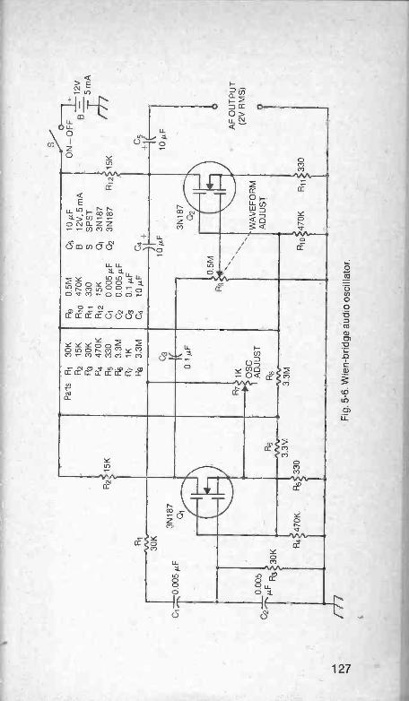
C17
-70
005
,LLF
R1
30K
3N18
7Q
t
R2
15K
Par
tsB
12V
. 5 m
A-O
FF
i:2V
Fli
30K
Rg
0.5M
C5
10 A
FO
NR
215
KR
1047
0K
T5
mA
R3
30K
R11
330
SS
PS
T
//
R5
330
R4
470K
R12
15K
Qi
3N18
7C
I0.
005µ
F02
3N18
7R
1215
KR
83.
3M02
0.00
5µF
R7
1K03
0.1
µFR
83.
3M04
10µF
03
0.00
5^µ
FR
330
K
R4
470K
R5
330
R6
3.3M
0 1
/IF
Fl1K O
SC
AD
JUS
T
R8
3.3M
10µF
3N18
702
0.5M
WA
VE
FO
RM
AD
JUS
T
R10
470
KR
1133
0
10µF
AF
OU
TP
UT
(2V
RM
S)
0
Fig
. 5-6
. Wie
n -b
ridge
aud
io o
scill
ator

V'
The output signal amplitude is approximately 2V RMS. Somewhat lower output voltage, at low impedance, may be
obtained across resistor RI,. If desired, resistor R11 may be replaced with a potentiometer for output voltage adjustment. -Current drain from the 12V supply is approximately 5 mA, but
this may vary somewhat with individual MOSFETs.
VILLARD AUDIO OSCILLATOR Figure 5-7 shows the circuit of another RC -tuned audio
oscillator having excellent sine -wave output. This circuit covers the range 200 Hz to 10 kHz in one rotation of the dual
potentiometer R5-R11. In this arrangement, tuning is accomplished with two phase -shift networks, C2-R5 and C3-R11, each of which
provides a total shift of 90°. The output of the 3 -stage amplifier (21 -Q2 -Q3 is fed back to the input stage ( via capacitor C,) in
the correct phase for positive feedback (and, accordingly, oscillation), after having undergone phase rotation in the Q4
auxiliary stage. (See the section Continuously Variable Phase Shifter, in Chapter 4, for further discussion.)
Oscillation control potentiometer Fla is set for oscillation at any setting of the frequency control R5-R11. Potentiometer
R,7 may then need to be reset for restoration of oscillation if R5-R1, is moved to a distant setting. ( When oscillation is
obtained at the low -frequency end of the frequency control, it will disappear at the high -frequency end, and vice versa,
unless R,7is reset.) The output signal amplitude at the AF output terminals is
approximately 2.5V RMS. A gain control potentiometer ( e.g., 10K) may be connected across these terminals if an adjustable
voltage is desired. The frequency control potentiometer may be provided with a dial calibrated to read directly in hertz.
Current drain from the 6V supply is approximately 40 mA, but this may vary somewhat with individual MOSFETS.
MULTIVIBRATOR Figure 5-8 shows the circuit of a conventional
drain -coupled multivibrator. This circuit is equivalent to the plate -coupled vacuum -tube multivibrator. With the circuit
constants given in Fig. 5-8, the output is an approximately square waveform of 4V peak -to -peak amplitude. As in the corresponding tube circuit, the operating
frequency depends upon the resistance and capacitance coupling components. Thus, C2 = C3, R = R4, and
f = 1/ ( 2irR,C2) ,
where f is in hertz, C2 in farads, and R, in ohms. The frequency may easily be changed to another
128
jiu

Par
ts
R1
1MR
61.
5MR
247
0KR
747
0KR
31.
5MR
810
00R
410
00R
g10
00 R
9R
5,11
DU
AL
R10
100
050
0K3N
187
R12
470K
R13
3.3M
R14
470K
1000
°01
22Q
1
R2
470K
R4
1000
1\3
C0
Ri5
470
A21
10K
C4
0 01
µF
R16
10K
C1
0.01
/IF
C5
0.00
5µF
R17
50K
C2
0.00
2µF
C.6
0.01
µF
R18
3.3M
C3
0.00
2µF
B6V
. 40
mA
Rig
470K
R10
100
0C
SS
PS
TR
2047
0IE-3
Q1
3N18
73N
187
0.00
2 µF
023N
187
03
nni
R8
1000
R7
470K
R14
470
K
050
005
/IF
R15
470
114
MU
ST
MA
TC
H R
g, A
ND
Fig
MU
ST
MA
TC
H R
10
Fig
. 5-7
. Vil
lard
osci
llato
r.
023N
187
Q3
3N18
704
3N18
7
R16
10K
3N18
7
3 3M R1Q
470K
R20
ON
-OF
Fqv
B=
-40
10K
T_
mA
C/
/0.
01 /I
F
AF
OU
TP
UT
(2.5
V R
MS
)
0

O
R3
1K
SO
N-
OF
F
B --1
6V-4
mA
T
240K
iii
02 I(0.
002
µF
1 p.
F
C3 )1
0.00
2 µF
3N18
7 2(
R4
240K
Fig
. 5-8
. Mul
tivib
rato
r.
C41
1- :1 µ
F
R5
1K
0.1
I.LF
Par
ts
R1
240K
R2
330
R3
1K
R4
240K
R5
1K
R6
330
OU
TP
UT
Ci
1µF
(4V
P -
P)
C2
0.00
2µF
C3
0.00
2µF
C4
1µF
C5
0.1
p,F
B6V
, 4 m
AR
6 33
0S
SP
ST
3N18
702
3N18
7

desired value by changing the resistances and capacitanceswhile preserving the relationships given above.
The multivibrator is essentially a positive -feedbackamplifier in which the drain of each stage feeds gate 1 of theother stage. The gate -2 electrodes are returned to the sources.The output wave will have best symmetry when the twoMOSFETs are closely matched; or, lacking this, when either R2or R6 is adjusted for matching of operating points.
Current drain from the 6V supply is approximately 4 mA,but this may vary somewhat with individual MOSFETs.
SUN -POWERED AUDIO OSCILLATORFigure 5-9 shows the circuit of a tickler -type audio
oscillator of the same type as that described earlier, but withthe battery replaced by two silicon solar cells PC, and PC2. Inbright sunlight, these two cells (International Rectifier S7M-C)deliver a total output of 6V and will adequately power theoscillator.
The output signal amplitude ( open -circuit) isapproximately 2.7V RMS; if transformer T, recommended inthe earlier circuit at the beginning of the chapter, is employedwith a C, capacitance of 0.018 µ,F, the frequency isapproximately 1000 Hz.
See the earlier section for a description of the amplifiercircuit alone.
SELF-EXCITED RF TICKLER -COIL OSCILLATORIn Fig. 5-10, an Armstrong -type radio -frequency oscillator,
oscillation is obtained with a tickler coil, LI, which feedsenergy from the output of the circuit into the input tunedcircuit L2-C2. The operating frequency is determined by thevalues of L2 and C2 according to
1
f = 6.28V L2C.2 (Eq. 5-6)
where f is in hertz, C2 in farads, and L2 in henrys.It is helpful to know also that, from rewriting Eq. 5-6,
L2 = 1/39.5 f2C2 and C2 = 1/39.5 f12. When C2 is a 365 pFvariable capacitor, coils may be wound as shown in Table 5-1to cover the frequency range of 440 kHz to 30 MHz in fivebands.
In this circuit, MOSFET Q receives its negative gate -1 biasfrom the voltage resulting from the flow of drain currentthrough source resistor R3, and its positive gate -2 bias from -voltage divider R1-R2. Resistance R, of this divider may
131

PC
1
BLU
EG
RE
EN
C1.
-'.
RE
D
10
ppb
ON
-O
FF
0
S7M
-C
S7M
-C
C2
±1(
1000
µF12
V
YE
LLO
W
50K
Re
4
3N18
7O
FE
ED
BA
CK
AD
JUS
T
Par
ts
R1
50K
B2
2K
C2
1000
µF
,12V
C3
0.1
µFC
425
µFP
C1
S7M
-CP
G2
S7M
-CS
SP
ST
O3N
187
SE
E T
EX
T F
OR
C1
AN
D T
R2K
C4
0.1
µF
25µF
AF
OU
TP
UT
(2.7
V R
MS
)
O
/1/
Fig
. 5-9
. Sun
-po
wer
ed a
udio
osc
illat
or.
111

C5
Par
ts
R1
150K
C5
0.00
5µF
R2
51K
B6V
, 1 m
AR
32K
SS
PS
TC
10.
002µ
F0
3N18
7C
30.
002µ
FS
EE
TE
XT
FO
R L
iL2
. AN
D C
2C
AI
0 01
ALF
L2
L1c
TU
NIN
G
SA
N-O
FF
B -
6V 1
mA
1
CA
)
150K
0 00
2 /IF
C3.
--,0
002
/IF
3N18
7
R2
51K
R3
2K
0 00
5 /..
t.F
O
RF
OU
TP
UT
(2V
RM
S)
0
1C
4001
AF
Fig
. 5-1
0. S
elf-
exci
ted
RF
osc
illat
or (
tickl
er ty
pe).
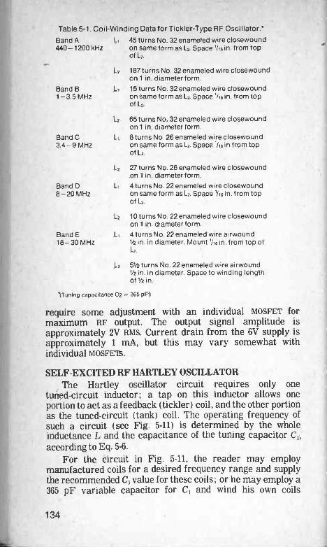
Table 5-1. Coil -Winding Data for Tickler -Type RF Oscillator.*
Band A 440-1200 kHz
Band B 1-3.5 MHz
Band C 3.4-9 MHz
Band D 8-20 MHz
Band E
18 - 30 MHz
L, 45 turns No. 32 enameled wire closewound on same form as L2. Space 1/16in. from top of L2.
L2 187 turns No. 32 enameled wire closewound on 1 in. diameter form.
L, 15 turns No. 32 enameled wire closewound on same form as L2. Space 1/16in. from top of L2.
L2 65 turns No. 32 enameled wire closewound on 1 in. diameter form.
Li 8 turns No. 26 enameled wire closewound on same form as L2. Space Vi6in from top of L2.
L2 27 turns No. 26 enameled wire closewound on 1 in. diameter form.
L, 4 turns No. 22 enameled wire closewound on same form as L2. Space 1/16in. from top of L2.
L2 10 turns No. 22 enameled wire closewound on 1 in. diameter form.
Li 4 turns No. 22 enameled wire airwound 1/2 in. in diameter. Mount 1/16,in. from top of L2.
L2 51/2 turns No. 22 enameled wire airwound 1/2 in. in diameter. Space to winding length of 1/2 in.
"(Tuning capacitance C2 = 365 pF.)
require some adjustment with an individual MOSFET for maximum RF output. The output signal amplitude is
approximately 2V RMS. Current drain from the 6V supply is approximately 1 mA, but this may vary somewhat with
individual MOSFETS.
SELF-EXCITED RF HARTLEY OSCILLATOR The Hartley oscillator circuit requires only one
tuned -circuit inductor; a tap on this inductor allows one portion to act as a feedback (tickler) coil, and the other portion
as the tuned -circuit (tank) coil. The operating frequency of such a circuit ( see Fig. 5-11) is determined by the whole
inductance L and the capacitance of the tuning capacitor C according to Eq. 5-6.
For the circuit in Fig. 5-11, the reader may employ manufactured coils for a desired frequency range and supply
the recommended C1 value for these coils; or he may employ a 365 pF variable capacitor for CI and wind his own coils
134

01
0.00
2 p.
FC
i,-*
- T
UN
ING
R1
C2
0.01
p.F
3N18
7
C5
Par
ts0.
002µ
FR
127
0
R2
1M
R3
470K
R4
1.8M
C2
0.01
/IF
C3
0.00
2µF
C4
0.00
5µF
C5
0.00
2µF
RF
C...
2.5
mH
C6
0.00
5 p.
F4t
iod
B7.
5V, 2
mA
RF
C 2
.5 m
HS
SP
ST
O3N
187
SE
E T
EX
T F
OR
L A
ND
C1
R4
1.8M
ON
-O
FF
RF
OU
TP
UT
(2.8
V R
MS
)
0
C6
-0 0
05R
470K
C4-
0 00
5 µF
FP
'F7
5V-
B-2
mA
Fig
. 5-1
1. S
elf-
exci
ted
RF
osc
illat
or (
Har
tley
type
).

Table 5-2. Coil -Winding Data for Hartley RF Oscillator.*
Band A 187 turns No. 32 enameled wire closewound 440-1200 kHz on 1 in. diameter form. Tap 45th turn from
ground end.
Band B 65 turns No. 32 enameled wire closewound 1-3.5 MHz on 1 in.diameter form. Tap 16th turn from
ground end.
Band C 27 turns No. 26 enameled wire closewound 3.4-9 MHz on 1 in. diameter form. Tap seventh turn from
ground end.
Band D 10 turns No. 22 enameled wire closewound 8-20 MHz on 1 in. diameter form. Tap second turn from
ground end. Band E 51/2 turns No. 22 enameled wire airwound
18-30 MHz 1/2 in. in diameter and spaced to winding length of 1/2 in. Tap second turn from ground end.
(Tuning capacitance ci365 pF.)
according to instructions given in Table 5-2, to give a frequency coverage of 440 kHz to 30 MHz in five bands.
In this circuit, MOSFET Q receives its negative gate -1 bias from the voltage drop resulting from the flow of drain current
through RF-bypassed source resistor R1, and its positive gate -2 bias from voltage divider R3-R4. Resistance R, in this divider may require some adjustment with an individual MOSFET for
maximum RF output voltage. The amplitude of the RF output voltage is approximately
2.8V RMS. Current drain from the 7.5V supply is approximately 2 mA, but this may vary somewhat with individual MOSFETS.
SELF-EXCITED RF COLPITTS OSCILLATOR Figure 5-12 shows the circuit of a Colpitts self-excited
radio -frequency oscillator. This circuit, like the Colpitts audio oscillator circuit described earlier, employs an untapped inductor ( L, )
, but a tapped capacitor leg ( C6-C7).
A dual variable capacitor (C6-C7) tunes inductor L to the desired frequency. Radio -frequency energy is coupled out of
the circuit by means of low -impedance coil L2. Refer back to the section Colpitts Audio Oscillator and Eq. 5-2 for
instructions for calculating the frequency of the Colpitts circuit in terms of inductance L, and the equivalent
capacitance of C. and C7 in series. Table 5-3 lists commercial RF coils which may be used with a dual 100 pF variable
capacitor to cover the four frequency bands shown, extending from 1.1 MHz to 25 MHz. These coils are slug -tuned and can be
preset for the exact band limits. In this circuit, MOSFET Q receives its negative gate -1 bias from the voltage drop resulting from the flow of drain current
136

Par
ts
Ri
27K
C4
100
pFR
225
KC
510
0 pF
R3
270
B9V
, 2 m
AR
41M
RF
C 2
.5 m
HR
55K
SS
PS
TC
10.
002µ
F0
3N18
7C
20.
01 µ
FS
EE
TE
XT
FO
RC
30.
01µF
L1, L
2, A
ND
Cg-
C7
SO
N-O
FF
B9V 2 m
A
3N18
7
R1
R21
1,0S
C
27K
25K
C17
-70.
002
µF
100
pF
Ra
270
C2
0.01
µF
R4
1 M
R5
5KG
3.-,
0 .0
1 p,
F
///F
ig. 5
-12.
Sel
f-ex
cite
d R
F o
scill
ator
(C
olpi
tts ty
pe)
L2
RF
OU
TP
UT
/II

Table 5-3. Coil Data for Colpitts RF Oscillator.'
cl
Band A 1.1-2.5 MHz
Band B 2.5 -5 MHz
LI Miller No. 20A474RBI (365 -564 µH).
L2 5 turns No. 24 enameled wire wound close to L.
LI Miller No. 20A104RBI (88.5 -120 p.H).
L2 5 turns No. 24 enameled wire wound close to L,.
Band C Li Miller No. 20A225RBI (16.2-26.4 µ1-4).
5-11.5 MHz 1-2 2 turns No. 24 enameled wire wound close
to L. Band D L, Miller No. 20A156RBI (1.08 -1.80 p.H).
10-25 MHz L2 1 turn No. 24 enameled wire wound close
to L,.
(Tuning capacitance C6-C7 = Dual 100 pF)
through source resistor R3, and its positive gate -2 bias from voltage divider R1- R2- R3. In this divider network, the
oscillation control is set for maximum RF output voltage. The RF output voltage will be of the order of 0.25V RMS. Higher voltage may be obtained by discarding L2 and taking
the output (through a 100 pF fixed capacitor) from the junction of the radio -frequency choke and the drain electrode of the
MOSFET. Current drain from the 9V supply is approximately 2 mA, but this may vary somewhat with individual mosFETs.
STANDARD CRYSTAL OSCILLATOR Figure 5-13 shows the circuit of a conventional crystal
oscillator in which the MOSFET replaces the vacuum tube or bipolar transistor. The only strange component is apt to be
capacitor C1, connected externally between drain and gate 1.
This capacitance is required for feedback coupling, since in most MOSFETs the internal capacitance is too small to sustain
oscillation. In all other respects, the circuit is conventional. The
resonant circuit L -C3 is tuned to resonate at the crystal frequency, and RF output voltage is taken from the top of the
tuned circuit through capacitor C,. The required L and C3 combination may be determined with the aid of Eq. 5-6 and its
accompanying discussion. Or, if a 100 pF variable capacitor is employed for C3, data will be found in Table 5-4 for coils covering the frequency range 680 kHz to 34 MHz in five bands. The RF output voltage is approximately 3V RMS. Current
drain from the 12V supply is approximately 2 mA, but this may vary somewhat with individual MOSFETS. The MOSFET receives
its negative gate -1 bias from the voltage drop resulting from
138

Il
25 p
i=
3N18
70
izni
za X
TA
L
RI
470K
R2
3 9K
0.01
;IF
C4
0.00
2µF
Par
ts
R1
470K
R2
3.9K
C1
25 p
FC
20.
01pc
C4
0.00
2C
50.
002µ
FB
12V
, 2 m
AR
FC
2,5
m1
-IS
SP
ST
RF
OU
TP
UT
3N18
7(3
V R
MS
)S
EE
TE
XT
FO
R C
3 A
ND
L
S0
0-O
N -
OF
F
- 12
VB
T2
mA
/II
Fig
. 5-1
3. S
tand
ard
crys
tal o
scill
ator
.

Table 5-4. Coil -Winding Data for Standard Crystal Oscillator.'
Band A 680 kHz -1.5 MHz
181 turns No. 36 enameled wire closewound on 1 in. diameter form.
Band B 57 turns No. 32 enameled wire closewound 1.8-4 MHz on 1 in. diameter form. Band C
3.8 - 8.6 MHz
Band D 8-18 MHz
Band E
15-34 MHz
25 turns No. 26 enameled wire on 1 in. diam- eter form.. Space to winding length of Y2 in.
12 turns No. 22 enameled wire on 1 in. diam- eter form. Space to winding length of 1/2 in.
51/2 turns No. 22 enameled wire on 1 in. diam eter form. Space to winding length of 1/4 in.
(Tuning capacitance C3 = 100 pF.)
the flow of drain current through source resistor R2. Gate 2 is returned externally to the source.
PIERCE CRYSTAL OSCILLATOR A MOSFET Pierce crystal oscillator is shown in Fig. 5-14.
The Pierce circuit has the advantage that it requires no tuned circuit. It is not useful, however, for overtone crystals, since
these crystals will oscillate in this circuit at their fundamental frequency rather than at the desired harmonic.
The open -circuit RF output voltage is approximately 3.2V RMS. Current drain from the 6V supply is approximately 1.6 mA, but this may vary somewhat with individual MOSFETS. The MOSFET receives its negative gate -1 bias from the voltage
drop resulting from the flow of drain current through source resistor R2.
SUN -POWERED RF OSCILLATOR Figure 5-15 shows the circuit of a tickler -type RF oscillator
of the same type as that described previously, but with the battery replaced by two silicon solar cells PC, and PC2. In
bright sunlight, these two cells (International Rectifier S7M-C) deliver a total output of 6V and will adequately power the
oscillator. The output signal amplitude ( open -circuit) is
approximately 2V RMS. If a 365 pF variable capacitor is used for C,, the coils described in Table 5-1 will permit tuning of the
oscillator over the range extending from 440 kHz to 30 MHz in five bands
The MOSFET receives its gate -1 negative bias from the voltage drop resulting from the flow of drain current through source resistor R4, and its gate -2 positive bias from voltage divider R,-R3. With an individual MOSFET, resistor R, in this divider may require some adjustment for maximum RF output
voltage.
140

R1
240K
/1/
XT
AL
01
C2
Par
ts
0.00
5 ,L
LF
R1
240K
R2
330
RF
C2.
5 m
H
R3
1K
Ci
0 1µ
FC
20
005
µFB
6V, 1
.6 m
AR
FC
2.5
mH
SS
PS
TQ
3N18
7
0 1
µF
Fig
. 5-1
4. P
ierc
e cr
ysta
l osc
illat
or.
R,3
1K
ON
-O
FF
6VB
T1
6 m
A
RF
OU
TP
UT
(3.2
V R
MS
)
0

PC
1
L1
ON
-OF
FR
ED
BLA
CK
RE
D
BLA
CK
L2 0 0 0
C2
0 00
2 µF
C1
TU
NIN
G
S7M
-C
S7M
-C
R1
150K
RF
C2.
5 m
H
R2
240K
3N18
7
51K
03
Cs
IE0.
005
µF
4
RF
OU
TP
UT
(2V
RM
S)
0
0 01
µF
/-7
Par
ts15
0KC
20.
002µ
FP
C1
S7M
-CO
. 3N
187
R2
240K
G3
0.00
2µF
PC
2S
7M-C
SE
E T
EX
T F
OR
A3
51K
C4
0.01
µFR
FC
2.5
mH
L2. A
ND
Ci
R4
2KC
50.
005µ
FS
SP
ST
Fig
. 5-1
5. S
un -
pow
ered
RF
osc
illat
or.
..iiii
0111
1111
1111
1111
1111
11&
.

C11
000
2
)
Cs
Tr
SE
C
1g"
11 C
; 1..E
:PR
I
Ti
K
S O
N O
FF
9VB
=-_
. 2 m
A
C2
002µ
F
R2
"VW
2.2M
jR3
470K
011
/I
C31
0.01
0.LF
R4
470K
Par
ts
R1
1K
R2
2.2M
R3
470K
R4
470K
R5
270
C1
0.00
2µF
C2
0.02
µFC
30.
01 µ
FC
40.
01 µ
FC
50.
02µF
B9V
. 2 m
AS
SP
ST
O3N
187
R5
0 0
7 !,
F
270
C
IF O
UT
PU
T
(3V
RM
S)
O
001
/IF
///F
ig. 5
-16.
Sel
f-ex
cite
d IF
osc
illat
or.

SELF-EXCITED IF OSCILLATOR Figure 5-16 shows the circuit of a self-excited
intermediate -frequency oscillator. This is a tickler -type oscillator with the two coils supplied by IF transformer T. The
latter is chosen for the intermediate frequency of interest-for example, 455 kHz, 1500 kHz, or 10.7 MHz. The transformer
must be connected in correct polarity for positive feedback; if the circuit does not oscillate when it is first tested, reverse the
connections to one of the transformer coils. The open -circuit IF output voltage is approximately 3V
RMS. Current drain from the 9V supply is approximately 2 mA, but this may vary somewhat with individual MOSFETS.
CRYSTAL -CONTROLLED IF OSCILLATORS If better stability is required than that afforded by the
self-excited IF oscillator described in the preceding section, a crystal oscillator may be used. Either of the crystal circuits
described earlier ( see Fig. 5-13 and 5-14) can be used. If the Pierce circuit is chosen (Fig. 5-14), it is necessary only to insert a crystal oscillating at the desired intermediate
frequency. If the standard circuit is used ( Fig. 5-13), inductor L and variable capacitor C3 can be supplied by one-half of an IF
transformer, and the output can be taken from the coil-capacitor circuit of the other half.
144

Chapter 6
Test Instruments
The unique characteristics of the MOSFET make it particularlysuitable for applications involving test instruments-expecially the miniaturized, battery -operated varitey.Important advantages obtained are negligible loading, reducedoperating current, gow drift, high sensitivity, and small size.
This chapter presents 15 selected instrument circuits.Several circuits appearing elsewhere in this book and intendedprimarily for other applications may also be used ininstrumentation. See, for example, Figs. 2-13 through 2-22, 3-1through 3-3, 3-12, 4-6, 4-12 through 4-14, 4-16, 4-17, 5-1 through5-8, 5-10 through 5-14, and 5-16.
In each of the circuits in this chapter, unless indicatedotherwise on the diagram or in the text, capacitances are inpicofarads, resistances in ohms, and inductances in henrys.Resistors are 1/2W, and electrolytic capacitors are rated at25V. For simplicity, batteries are shown for DC supply;however, a well filtered power -line -operated power supplymay be used instead.
Before undertaking the wiring or operation of any circuitin this chapter, read carefully the hints and precautions givenin Chapter 1.
SINGLE-MOSFET ELECTRONIC DC VOLTMETERFigure 6-1 shows a simple electronic DC voltmeter circuit
offering an input resistance of 11M, adapted from a circuit by
145

0)
R1
1M
TR
(5B
Ej--
- 1
GR
OU
ND
) S
HIE
LD!
CLI
P
Par
ts
R1
1M
R2
7M
R3
2M
R4
700K
R5
200K
R6
70K
R7
20K
R8
10K
Rg
1K
R10
4700
R11
2KW
WR
1239
0R
13 2
KW
WR
1412
00C
0.00
1 A
FB
9V, 5
.5 m
AM
0-10
0 D
C A
AS
1S
P7T
S2
SP
ST
O3N
187
05V
015V
050V
0 15
0V
0500
V
3N18
7
C00
1µF
/I
R12
0-10
0 D
C p
.A R13
-111
,2K
WW
CA
LIB
RA
TIO
N
R14
4700
4
Fig
. 6-1
. Sin
gle-
mO
sFE
T e
lect
roni
c oc
vol
tmet
er.
390
2K W
WZ
ER
O S
ET
1200
ON
-
XIF
FS
2 O
+9V
B=
5 5
mA

Siliconix. This arrangement is seen to be similar to thevacuum -tube counterpart. Seven voltage ranges are employedbetween 0.5V full-scale and 500V full-scale.
As in most conventional electronic voltmeters-tube-typeand transistorized-the indicating microammeter is connectedin a bridge circuit of which the internal drain -to -sourceresistance of the MOSFET is a part. With zero -signal input tojack J, the meter is set to zero by balancing this bridge(potentiometer R13 is the balancing element ) . When a DCvoltage subsequently is applied at jack J, the bridgeunbalances (since the MOSFET drain resistance changes), andthe meter reads proportionately.
The accuracy of the instrument depends in large part uponthe precision of resistors R, to R8 in the input circuit. Specialclose -tolerance instrument resistors must be obtained, or theodd values must be made up by connecting several lowervalues in series.
Initial calibration is straightforward:(1) With zero voltage at the input probe, close switch S2
and set potentiometer R13 tozero the pointer of meter M ( rangeswitch S, may be at any setting for this operation).
(2) Set range switch S, to its 1.5V position.(3) Connect an accurately known 1.5V source to the input
probe and ground clip.(4) Adjust calibration control R for exact full-scale
deflection of meter M.(5) Temporarily remove the input voltage and note
whether meter is still zeroed. If it is not, reset R13-(6) Work back and forth between steps 3, 4, and 5 until a
1.5V input deflects the meter to full scale, and the meterremains zeroed when the 1.5V input is removed. PotentiometerRi, will not need to be reset unless its setting is disturbed or theinstrument is being periodically recalibrated. Zero -setpotentiometer R13 will need to be reset before each period ofuse.
The RC filter formed by R9 and C serves to remove any ACcomponents and hash that enter the input section of the circuit.The 1M resistor R, in the shielded probe protects the circuitfrom hand capacitance.
Current drain from the 9V supply is approximately 5.5 mA,but this may vary somewhat with individual MOSFETs.
BALANCED ELECTRONIC DC VOLTMETERThe circuit shown in Fig. 6-2, like its tube or transistor
counterpart, requires less zero resetting than a single -endedcircuit does, if a pair of MOSFETs with matched characteristics
147

Co
Par
ts
R1
5MR
640
KR
1110
0B
6V, 1
.6 m
AR
2 4M
R7
5KR
121K
S1
SP
8TR
350
0KR
85K
Ri3
1K W
WS
2S
PS
TR
440
0KR
91K
R14
2KM
0-50
DC
p.A
R5
50K
R10
1K
C0.
001
/IFQ
13N
187
-02
3N18
7
RA
NG
E
RiZ
5M00
5V
1Vo
R R3
4M5V
Rg
500K
1K
+0
C-
010V
R4
0 00
1
DC
INP
UT
400K
o 50
V///
R5
50K
0100
VR
640
K
5K05
00V
o100
0V
R7
R8
5K
/ / /
3N18
7
Qi
R13
ZE
RO
SE
T
A10
1K
1K W
WM
0-50
DC
iLA
+ R
14 C
AL
2K 3N18
7
QZ
iR11
100
R12
1K
Fig
. 6-2
. Bal
ance
d el
ectr
onic
DC
vol
tmet
er.
/ / /
ON
--
\I1F
FS
2
B6V
=1
6 m
A
is used. Any drift in MOSFET Q, is balanced out by comparabledrift in Q2; the internal drain circuits of the MOSFETS, inconjunction with resistors R10, R11, R12, and R13, form a bridgefor this purpose and for the normal operation of the voltmeter.Indicating microammeter M is the detector in this bridgecircuit. With zero signal at the input terminals. the meter is setto zero by balancing this bridge (potentiometer R13 is thebalancing element). When a DC voltage subsequently is appliedat the input terminals, the bridge unbalances ( since the drainresistance changes), and the meter reads proportionately.
The input resistance of the instrument is 10M. Eightvoltage ranges are provided between 0.5V full-scale and 1000Vfull-scale. The accuracy of the instrument depends in largepart upon the precision of resistors R, to R8 in the input circuit.Special close -tolerance instrument resistors having the exactvalues shown in Fig. 6-2 must be obtained, or the odd valuesmust be made up by connecting several lower values in series.
Initial calibration is straightforward:( 1) With zero voltage at the input terminals, close switch
S2 and set potentiometer R13 to zero the pointer of meter M( range switch S, may be at any setting for this operation).
(2) Set range switch S, to its 1V position.( 3) Connect an accurately known DC source of 1V to the
input terminals.( 4) Adjust calibration control R14 for exact full-scale
deflection of meter M.( 5) Temporarily remove the input voltage and note
whether or not the meter is still zeroed. If it is not, reset R13.( 6) Work back and forth between steps 3, 4, and 5 until a 1V
input deflects the meter to full-scale, and the meter remainszeroed when the 1V input is removed. Rheostat R14 will notneed to be reset unless its setting is disturbed or theinstrument is being periodically recalibrated. Zero setpotentiometer R13 will not need frequent readjustment unlessits setting is accidentally disturbed.
The RC filter formed by R9 and C serves to remove any ACcomponents and hash that enter the input section of the circuit.No further filtering or bypassing is required.
Current drain from the 6V supply is approximately 1.6 mA,but this may vary somewhat with individual MOSFETs.
CENTER -ZERO ELECTRONIC DC VOLTMETERFigure 6-3 shows an electronic DC voltmeter circuit in
which the indicating meter is initially set to place zero at thecenter of the scale. A positive input voltage then will deflectthe meter up from center -scale, whereas a negative voltage
149

0 1 0
1V
O+
DC
INP
UT
OC
OM
R1
9M
R2
900K
0
Si
RA
NG
E
10V
R5
1K
100V
R3
90K
O
1000
V
R4
10K
O
C -
0 00
2 A
F
//
Par
ts
R1
9MR
290
0KR
390
KR
410
K
R5
1K
R6
50K
WW
R7
5K W
W
R8
47K
C0
002
µFB
6V, 5
mA
M0-
5 D
Cm
AS
tS
P4T
S2
SP
ST
O3N
187
R8
47K
Re
50K
R7
5KW
WZ
ER
O W
WC
ALI
BR
AT
ION
SE
T
Iii
Fig
. 6-3
. Cen
ter
-zer
o el
ectr
onic
DC
vol
tmet
er.
ON
-
XIF
FS
2
V
BT
65m
A

will deflect it downscale, and the input leads will not need to beswapped.
The input resistance of the instrument is IOM on allranges. Four voltage ranges are provided between 1Vfull-scale and 1000V full-scale. The accuracy of the instrumentdepends largely upon the precision of resistors R, to R4 in theinput circuit. Special close -tolerance instrument resistorshaving the exact values given in Fig. 6-3 must be obtained, orthe odd values must be made up by connecting several lowervalues in series.
The instrument is initially calibrated in the followingmanner:
(1) With zero voltage at the input terminals, close switchS2 and set potentiometer R6 to zero the pointer of meter M( range switch S, may be at any setting for this operation).Remember that the zero point is center -scale, i.e., at the 2.5mA point on the scale of this 5 mA meter.
(2) Set range switch SI to its 1V position.(3) Connect an accurately known source of +1V to the
input terminals.(4) Adjust calibration control R, for full upscale deflection
of the meter.( 5) Reverse the DC source, applying -1V to the input
terminals. The meter should now show full downscaledeflection.
(6) Temporarily remove the input voltage and notewhether or not the meter is still zeroed. If it is not, reset R6.
(7) Work back and forth between steps 3, 4, 5, and 6 until a+1V input deflects the meter full-scale upward, a -1V inputdeflects it full-scale downward, and the meter remains zeroedwhen the DC input is removed. Rheostat R, will not need to bereset unless its setting is accidentally disturbed or theinstrument is being periodically recalibrated. The reader mustdraw a special scale for the meter, having zero at the center.
The RC filter formed by R5 and C serves to remove any ACcomponents and hash that enter the input section of the circuit.No further filtering or bypassing is required.
Current drain from the 6V supply is approximately 5 mA,but this may vary somewhat with individual MOSFETS.
CRYSTAL -TYPE FREQUENCY STANDARDFigure 6-4 shows the circuit of a 100 kHz frequency
standard employing a Pierce crystal oscillator. The advantageof the Pierce circuit is its freedom from tuning; noadjustments are needed to start the oscillation-simply plug inthe crystal and close the power switch.
151

03
XTAL Imo 100 kHz
3N187
50 pF R1 470K
0.1µF
R2 330
25 pF
RFC 25 mH
F3 1K
ON-OFF
S
Bi 6V T1.6 mA
RF OUTPUT (3V RMS)
O
Parts
R1 470K R2 330 R3 1K C1 50 pF C2 0 1 /AF C3 25 pF B 6V. 1.6 mA
RFC 25 mH S SPST Q 3N187
Fig. 6-4. Crystal -type frequency standard.
In this arrangement, C, is a small trimmer -type capacitor which allows the frequency to be varied a few cycles on either
side of 100 kHz for standardizing against wwv transmissions or some other accurate source.
The signal amplitude at the output terminals is approximately 3V RMS. Current drain from the 6V supply B is approximately 1.6 mA, but this may vary somewhat with individual MOSFETS.
SELF-EXCITED FREQUENCY STANDARD A self-excited 100 kHz oscillator is satisfactory for use as a secondary standard and spotting oscillator when the very high
stability and accuracy of a crystal -controlled oscillator is not required. Figure 6-5 shows a self-excited circuit of the tickler
type.
152

C4
100
kHz
IF T
RA
NS
FO
RM
ER
Ti
lath
I
Tal
ia
3N18
7
ON
-O
FF
B -
6V lm
A
150K
C1.
--77
0.00
5 /IF
C2
0 00
5 p.
F51
K
Fig
. 6-5
. Sel
f-ex
cite
d fr
eque
ncy
stan
dard
.
R3
0.00
1 tiF
Par
ts
R1
150K
R2
51K
R3
2KC
10.
005µ
FC
20.
005µ
FC
30.
01 A
FC
40.
001
/IFB
6V. 1
mA
SS
PS
TQ
3N18
7
2K
RF
OU
TP
UT
(2V
RM
S)
C 3
,-, 0
0 1
AF

In this arrangement, the signal and tickler windings both are supplied by 100 kHz intermediate -frequency transformer T
( Miller No. 1890-P4). This is a slug -tuned transformer, and the slugs may be adjusted to zero -beat the oscillator with wwv
transmissions. At this low frequency, the circuit is surprisingly stable. Polarity of the transformer is important;
if oscillation does not occur, reverse the connections of either the primary or the secondary (not both).
The MOSFET receives its negative gate -1 bias from the voltage drop resulting from the drain current through
RF-bypassed source resistor R3, and its positive gate -2 bias from voltage divider R,-R2. Resistance R, in this divider may need some adjustment with an individual MOSFET for highest
RF output. Open -circuit output voltage is approximately 2V RMS.
Current drain from the 6V supply is approximately 1 mA, but this may vary somewhat with individual MOSFETS.
AF-RF SIGNAL TRACER Figure 6-6 shows the circuit of a signal tracer for following
either an AF or RF signal through an electronic system, and which provides either visual indication ( meter) or aural
indication ( loudspeaker). High input impedance is provided for either mode.
This arrangement consists of the combination MOSFET-IC 1/4W -output audio amplifier described earlier ( see MOSFET
Input for lc Amplifier, Chapter 2), provided with AF and RF probes and a metering circuit (D2-R2-M).
The AF probe consists of shielded envelope and shielded cable with a 0.1 t.LF series capacitor. The RF probe is a
demodulator type for following a modulated signal through a circuit, and it consists of shunt demodulator diode D1, input
capacitor C,, load resistor R,, and output envelope -coupling capacitor C2. This probe also is shielded. Shielded input jack J
is provided for connecting the probes to the amplifier. When switch S is in position 1, the speaker is connected to
the output of the amplifier and the signal is made audible. When S is in position 2, a rectifier -type meter ( composed of
0-1 DC milliammeter M, 1N34A germanium diode D2, and 10K wirewound rheostat R2) is connected to the output winding of
the output transformer in the amplifier. The diode rectifies the output signal and deflects the meter proportionately, thus
providing a visual signal. Rheostat R2 is set to keep the meter from exceeding full-scale deflection on strong test signals.
The amplifier and, accordingly, the signal tracer itself, requires a 6V DC supply. The zero -signal current drain is 14
154

0.1 µFSHIELDED CABLE -J
GROUNDCLIP
MOSFET IC AMPLIFIER(SEE FIG 2-7 CHAPTER 2)
I Ci
10 01 µF 0 1 F
D1 240KL1N34A
GROUNDDEMODULATOR PROBECLIP
PartsR1 240KR2 10K WWCr 0 01 µFC2 0.1 µF
Fig. 6-6. Signal tracer(AF -RE).
D1 1N34AD2 1N34AM 0 1 DC mAS SPST
mA, and the maximum -signal current drain is 87 mA; butthese may vary somewhat with individual MOSFETs and Ics.
TUNED RF -IF SIGNAL TRACERWhile aperiodic signal tracers such as the one described in
the preceding section are easy to build and simple to use,professional signal tracing-especially in the RF and IF stagesof radio and television receivers-often requires that theinstrument be closely tuned to the traced signal. Tuned signaltracers can be very complicated. Figure 6-7, however, shows afairly simple circuit that gives good selectivity and sensitivity.An electronic DC voltmeter ( either vacuum -tube ortransistorized) is connected to its output terminals to serve asthe visual indicator.
The input of the circuit is of high impedance and untuned,the signal being coupled into the circuit through capacitor C,and resistor R,. The signal is picked up with a shielded probe( of the simple test -meter type) plugged into jack J. The outputof the circuit is tuned by means of C5 and L. A set of five plug-incoils may be wound for L to cover a tuning range from 440 kHzto 30 MHz with the 365 pF variable capacitor C5. Table 5-1 inChapter 5 gives winding instructions for these coils (in usingthis table, take the L2 data for each coil; ignore the L, values,since the signal tracer coil will not have a tickler).
Output of the tuned circuit is coupled through capacitor C6to a shunt rectifier circuit (germanium diode D and load
155
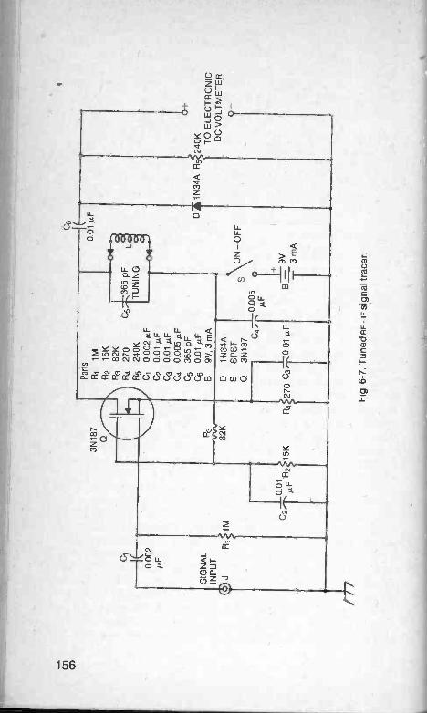
rn
3N18
7
C6
Par
ts
R1
1M
R2
15K
0.01
'IF
R3
82K
R4
270
C5,
7-73
65pF
L3R
524
0KT
UN
ING
0 00
2C
i0.
002µ
FC
20.
01 p
lC
30.
01 p
lC
40.
005
tA.F
0+C
536
5 pF
C6
0.01
I.LF
DA
1N34
A R
5 24
0KS
IGN
AL
B9V
, 3 m
AT
O E
LEC
TR
ON
ICIN
PU
TD
C V
OLT
ME
TE
R82
KD
1N34
A1M
0-S
SP
ST
Q3N
187 C
4-0.
005
S\\O
N-O
FF
p.F
01µF
F R
215
KR
427
0 C
30
01 µ
FF
B=
9V 3 m
A
Fig
. 6-7
. Tun
ed R
F -
IF s
igna
l tra
cer.
resistor R5). The resulting DC output of the rectifier, at theoutput terminals, drives the external voltmeter. When usingthe tracer, variable capacitor C5 is simply tuned for maximumdeflection of the meter.
In this circuit, the MOSFET receives its negative gate -1 biasfrom the voltage drop resulting from the flow of drain currentthrough source resistor R4, and its positive gate -2 bias fromvoltage divider R2 -R3. In this divider, resistance R3 may needsome adjustment for maximum output. Current drain from the9V supply is approximately 3 mA, but this may vary somewhatwith individual MOSFETs.
AF SIGNAL -TRACER ADAPTER FOR AC VOLTMETERThe 2-MOSFET circuit shown in Fig. 6-8 allows a
low -resistance AC voltmeter ( 100011 or 500012 per volt) to beused for audio -frequency signal tracing. The input impedanceseen by the signal source is 0.1 iLF ( C,) in series with 1M (R,).The first stage is a common -source RC amplifier; the secondstage is a source follower delivering output to the meter from5000 resistor R7. Overall voltage gain of the system isapproximately 15 (that is, 30 for the input stage and 0.5 for theoutput stage). With sensitivity control R, set for maximumsensitivity, the maximum input signal at jack J before peakclipping in the output is approximately 50 mV RMS. Thecorresponding signal at the output terminals0.75V RMS. This provides a good deflection on the 0-1.5V rangeof the AC voltmeter connected to these terminals. A simpleshielded probe may be plugged into jack J.
In this circuit, MOSFET Q, receives its negative gate -1 biasfrom the voltage drop resulting from the flow of drain currentthrough source resistor R4, and its positive gate -2 bias fromvoltage divider R2 -R3. In this divider, resistance R3 mayrequire some adjustment for maximum signal output. Theother MOSFET, Q2, receives its negative gate -1 and gate -2 biasfrom the voltage drop resulting from the flow of drain currentthrough source resistor 14 Current drain from the 12V supplyis approximately 4 mA, but this may vary somewhat withindividual MOSFEIS.
ACTIVE PROBEFigure 6-9 shows the circuit of a probe (useful with such
instruments as oscilloscopes and meters) that provides notonly voltage gain (10, open -circuit), but also high inputimpedance (1µF capacitor C1 in series with 10M resistor 13,1)and wideband frequency response ( -3 dB at 50 Hz and -6 dBat 10 MHz). This circuit must be carefully shielded and itsleads individually dressed, all according to wideband practice.
157

01C
3C
ID
0.1µ
F
AF
INP
UT
Loj
J
/ J /
I
R1
1M SE
NS
ITI-
VIT
Y
3N18
70.
1 µF
Qi
15K
3N18
7
G2
Par
ts
R1
1M
R2
470K
R3
3.3M
R4
3,3K
R5
15K
R6
1M
R7
500
C1
0.1
/IF02
50µF
C3
0.1µ
F04
50µF
Cs
1µF
B12
V, 4
mA
SS
PS
TCh
3N18
702
3N18
7
I
I(1
µF
ON
-OF
FA
F
500(
TO
VM
)OU
TP
UT
1-12
VB-4
mA
Fig
. 6-8
. Aud
io -
freq
uenc
y si
gnal
-tr
acer
ada
pter
for
AC
vol
tmet
er.
s\

PR
OD
GR
OU
ND
At
CLI
P
01 ci)
10M
R2
15K
C.2
3N18
7
F16
1K
C6
1µF
SH
IELD
ED
CA
BLE
L g
33 µ
Fi (
SE
E T
EX
T)
1300
pF
ON
OF
F
0.00
5
pi9V
B - - 3
mA
Fig
. 6-9
. Act
ive
prob
e.
OU
TP
UT
Par
ts
R1
10M
R2
15K
R3
82K
R4
47
R5
220
R6
1K
C1
1µF
C2
0.01
/IF
C3
300
pFC
45
µF. 1
6VC
5 0.
005µ
FC
,61
p.F
B9V
. 3 m
AL
33 µ
H (
SE
E T
EX
T)
SS
PS
TQ
3N18
7

The 33 µII inductor L is a Miller 9250-333 molded RF choke. It provides compensation in this video amplifier circuit, as
does the 300 pF miniature trimmer capacitor C3. The latter must be rigidly mounted in such a position that its adjusting
screw is easily reached through a hole in the probe housing. Set C3 for best overall frequency response.
In this circuit, the MOSFET receives its negative gate -1 bias from the voltage drop resulting from the flow of drain current
through the source -resistor combination ii4-R5 (bypassed separately for both low and high frequencies)
, and its positive
gate -2 bias from voltage divider R2-R3. In this divider, resistance R3 may need some adjustment for minimum distortion in the output signal. Current drain from the 9V
supply is approximately 3 mA, but this may vary somewhat with individual MOSFE1S.
WIDE -RANGE LC CHECKER Figure 6-10 shows the circuit of a checker which allows a
variable -frequency audio generator (tuning from 20 Hz to 20 kHz) to be used to measure inductance from 6.3 mH to 6329H and capacitance from 0.0632 /IF to 63,291 µF. Other ranges for
capacitance may be obtained by changing the value of inductor L, and other ranges of inductance may be obtained by
changing the value of capacitor C2.
The MOSFET provides a source -follower circuit which drives a series -resonant circuit containing the unknown
capacitance connected in series with a known inductance, L,
or the unknown inductance connected in series with a known capacitance, C2. The generator is tuned for peak deflection of
meter M, which is part of an AC milliammeter connected in the series -resonant circuit. At that point, the generator frequency
is noted, and the unknown component calculated in terms of the known values. Thus, Cx = 1/39.5f 2L3 and Li = 1/39.5f ts.
The unknown component is connected to terminals x-x. Resonant current flowing through 10011 resistor R3 develops a
voltage drop across this resistor, and this voltage is rectified by diode D to deflect meter M. Standard inductor L is a 1 mH
slug -tuned coil (Miller 22A103RBI) which may be set exactly to 1 mH in a suitable bridge. Standard capacitor C2 is a 0.01 µF
silver -mica unit which must be obtained with as high accuracy as practicable.
Capacitance Measurement To use the instrument for determining capacitance values, follow this procedure:
(1) Connect the signal generator to the AF input terminals.
160

Cl
F01
µF
AF
INP
UT
(FR
OM
OS
CIL
LAT
OR
OR
SIG
NA
LG
EN
ER
AT
OR
)O
0.5
M
SE
NS
ITIV
ITY
R2
150
C3 /
L
6101
51
mH
(SE
E T
EX
T)
c
Par
ts
R1
0.5M
S2:
:)N
1- O
FF
R2
500
F3
100
Ci
0.1
µFC
20.
01 ;I
F7.
5VC
350
µFQ
- 2 m
AC
40.
05µF
B7.
5V, 2
mA
D1N
34A
M0-
50 D
C µ
AS
PD
TS
2S
PS
TO
3N18
7L
1 m
H (
SE
E T
EX
T)
C4
500
0.01
µF
UN
KN
OW
N C
OR
LC
ON
NE
CT
ED
HE
RE
R3
X 100
0 05
I.L.
F
M
D1N
34A
CY
)F
ig. 6
-10.
Wid
e -r
ange
LC
che
cker
.
0-50
DC
µA

(2) Connect the unknown capacitor to terminals x-x. (3) Set switch S, to c. (4) Close switch S2 and turn on generator.
( 5) Tune generator throughout its range, watching for a peak deflection of meter M.
(6) At peak, read frequency f from generator dial. (7) Calculate the capacitance: C = 1/0.0395/2, where C is
in farads and f in hertz. Note that the formula is simplified, since the inductance of L is constant.
Inductance Measurement The following steps describe the sequence for measuring
inductance. (1) Connect the signal generator to the AF input terminals. (2) Connect the unknown inductor to terminals x-x.
( 3) Set switch S, to L.
(4) Close switch S2 and turn on generator. ( 5) Tune generator throughout its range, watching for a peak deflection of meter M. ( 6) At peak, read frequency f from generator dial.
(7) Calculate the inductance: L = 1/3.95/2 x 10 -7, where L is in henrys and fin hertz. Note that the formula is simplified,
since the capacitance of C2 is constant. In this circuit, the MOSFET receives its negative gate -1 and
gate -2 bias from the voltage drop resulting from the flow of drain current through source resistor R2. Current drain from
the 7.5V supply is approximately 2 mA, but this may vary somewhat with individual MOSFETs.
AC NULL DETECTOR A sharply tuned null detector is an asset in balancing an AC
bridge, and it is important also that the input impedance of the detector be high. Figure 6-11 shows a null -detector circuit meeting these specifications. This arrangement consists of the
RC -tuned peak amplifier described in Chapter 2, followed by a simple AC meter circuit ( C-D1- D2-R -M)
. For the common 1000 Hz bridge frequency, the frequency -determining resistances and capacitances in the amplifier ( see Fig. 2-18) are: C2 = C3 = 0.1 iLF, C4 = 0.2 µF,
R3 = R5 = 159211, and R4 = 79611. The gain control in the amplifier can be used to set the prenull deflection of meter M to full-scale. Rheostat R in the
metering circuit is preset for full-scale deflection of meter M when the amplifier gain control is in its maximum -sensitivity
position.
162

PartsR 10K WWC 1µF
1N34AD2 1N34AM 0-100 DC p.A
FROM BRIDGEOUTPUT
RC -TUNEDAF PEAK AMPLIFIER AF
INPUT (SEE FIG. 2-18, OUTPUTCHAPTER 2)
1µF
Fig. 6-11. Alternating -current null detector.
10K WW
0-100DC µA
SENSITIVE LIGHT METERFigure 6-12 shows the circuit, which increases the
sensitivity of a self -generating selenium photocell. The circuitis basically that of a MOSFET DC amplifier which drives a 0-100DC microammeter. The meter is connected in a 4 -arm bridgecircuit in the output of the MOSFET. The arms of this bridgeconsist of resistors R2, R3, and R4 and the internaldrain -to -source resistance of the MOSFET.
Initially, with photocell PC (International RectifierB3M-C1) darkened, the bridge is balanced and the meter,therefore, zeroed by adjustment of rheostat R4. For thisoperation, potentiometer R1 should be set to itsmaximum -sensitivity position. When subsequently thephotocell is illuminated, the resulting output voltage drives theMOSFET gates positive; and this changes the internalresistance of the MOSFET, unbalancing the bridge and causingthe meter to deflect proportionately.
Illumination of 10 footcandles results in full-scaledeflection of the meter. By comparison, if the photocell isconnected directly to the microammeter, illumination of 100footcandles will give approximately 75% of full-scaledeflection. If facilities for calibration are available, a dialattached to potentiometer R1 may be graduated to readdirectly in footcandles.
Current drain from the 6V supply is approximately 3 mA,but this may vary somewhat with individual MOSFETS.
SINE- TO SQUARE -WAVE CONVERTERFigure 6-13 shows an aperiodic ( untuned) circuit for.
converting input sine waves into output square waves. This
163

rn
41.
PC
RE
D
B3M
-C
BLA
CK
R1
3N18
70
4-
50K
WW
SE
NS
ITIV
ITY
R2
470
R4
ZE
RO
SE
T5K
WW
0- 1
00 D
C µ
A
Par
ts
R1
50K
WW
R2
470
R3
470
R4
5K W
WB
6V 3
mA
M0-
100
DC
p.A
6V
PC
B3M
-CB
-= 3
mA
SS
PS
T0
3N18
7
R3
vv,
470
S \O
N-O
FF
Fig
. 6-1
2. S
ensi
tive
light
met
er.

NU
SIN
E -
WA
VE
INP
UT
0
F
Fii
0.47
M
11/4
S \O
N-O
FF
I6V
B3N
187
- 0
5 m
AT-
02
1
R4
1K
R3
10K
02 (
SE
E T
EX
T)
SQ
UA
RE
-W
AV
EO
UT
PU
T
Fig
. 6-1
3. S
ine-
to s
quar
e -w
ave
conv
erte
r.
Par
ts
R1
0.47
MR
210
K
R3
10K
R4
1K
Ci
0.1
µFC
2 S
EE
TE
XT
B6V
, 0.5
mA
SS
PS
T01
33N
1188
7702
N

arrangement consists essentially of cascaded overdriven stages coupled by common source resistor R4.
The minimum input signal amplitude for good square -wave shape is 0.8V RMS. In some instances, especially Where the sine -wave signal source has low output, the input
voltage of the converter may be derived from an intermediate amplifier stage (see, for example, Fig. 2-1, Chapter 2).
Capacitor C2 will be required when the output load device would short-circuit the drain of MOSFET Q2. The actual
capacitance will depend upon the resistance and reactance of the load; it must be determined experimentally, that value
being chosen which will least distort the square waveform. In most instances, 1µF will be suitable.
Current drain from the 6V supply is approximately 0.5 mA, but this may vary somewhat with individual MOSFETS.
AM MONITOR Figure 6-14 shows the circuit of a sensitive monitor for amplitude -modulated signals. Operable at some distance from
the transmitter, the device receives its signal through a small pickup antenna, which may be a standard whip antenna or simply a vertical length of stiff wire or rod.
The signal is tuned in with inductor L and capacitor C2. For general -coverage tuning from 440 kHz to 30 MHz, C2 is a 365 pF
variable capacitor, and plug-in coils may be wound according to the instructions given in Table 4-1, Chapter 4.
The signal is demodulated by 1N34A diode D, and the resulting AF envelope, corresponding to the modulation, is
presented to gate 1 of the MOSFET through volume control H2.
The MOSFET functions here solely as an AF amplifier, providing the sensitivity of the monitor.
A high -impedance headset or earpiece may be connected directly to the output terminals; or, for a louder signal, a suitable amplifier and speaker ( see, for example, Fig. 2-7, Chapter 2) may be connected.
In this circuit, the MOSFET receives its negative gate -1 bias from the voltage drop resulting from the flow of drain current
through source resistor R5, and its positive gate -2 bias from voltage divider R3-R4. Resistance R4 in this divider may require some adjustment for maximum output. Current drain
from the 9V source is approximately 2 mA, but this may vary somewhat with individual mosFurs.
CW MONITOR Figure 6-15 shows the circuit of a sensitive monitor for cw
signals. Operable some distance from the transmitter, the
166

0)
PIC
KU
P A
NT
EN
NA
50 p
F
DP
O-
1N34
A
C2'
'4 3
65 p
F. T
UN
ING
/ //
R1
1K
C4
0.1
/IF
0 00
5
N-I
OLU
ME
3N18
70
R3
470K
R5
330
Fig
. 6-1
4. M
onito
r fo
rAM
.
R1
1KP
arts
R2
1M
R3
470K
R4
3.3M
R5
330
R6
1KC
150
pF
C2
365
pFC
30.
005µ
FC
40.
1 i.L
F
C5
50µF
C6
0.1
p.F
B9V
, 2 m
AD
1N34
AS
SP
ST
C)
3N18
7S
EE
TE
XT
FO
R L
C6
0.1
µF
Rs
1K
AF
OU
TP
UT
(TO
HE
AD
PH
ON
ES
OR
TO
AM
PLI
FIE
R A
ND
SP
EA
KE
R)
0
ON
-OF
F

rn
OD
PIC
KU
P A
NT
EN
NA
1,50
pF
C2
365
pFT
UN
ING
Par
ts
R1
270
C4
0.00
5µF
R2
470K
C5
0.00
5µF
R3
4.7K
C6
0.1
/.1.F
R4
25K
C7
0.00
5µF
R5
27K
B9V
, 2 m
AR
61K
SS
PS
TC
150
pF
03N
187
G2
365
pFS
EE
TE
XT
FO
R L
G3
100
pF
/
C3 I(
100
pF R1
270
C,1
0 00
5 p.
F
3N18
70..
R2
470K
C6
R3
4.7K
1
AF
OU
TP
UT
(TO
HE
AD
PH
ON
ES
OR
TO
AM
PLI
FIE
RA
ND
SP
EA
KE
R)
0R
4R
5
25K
27K
\ON
-O
SC
ILLA
TIO
NS
OF
F
0 00
5 A
FQ
C7,
-, 0
.005
µF
B9V
-2 m
A
Fig
. 6-1
5. M
onito
r fo
r cw
.

device is essentially an oscillating detector which receives itssignal through a small pickup antenna. The latter may be astandard whip antenna or a vertical rod or wire.
The signal is tuned in with inductor L and capacitor C2. Forgeneral -coverage tuning from 440 kHz to 30 MHz, C2 is a 365 pFvariable capacitor, and plug-in coils may be wound accordingto the instructions given in Table 5-2, Chapter 5.
In this circuit, oscillation ( regeneration) is controlled byadjustment of rheostat R4 in the voltage divider which suppliespositive bias to gate 2 of the MOSFET. This control is set for themost pleasing tone. Gate 1 receives its negative bias from thevoltage drop resulting from the flow of drain current throughthe RF-bypassed source resistor RI. High -resistanceheadphones may be connected directly to the outputterminals; for louder signals, an amplifier and speaker (see,for example, Fig. 2-7, Chapter 2) may be connected instead.
Current drain from the 9V supply is approximately 2 mA,but this may vary somewhat with individual MOSFETS.
169

Chapter 7
Miscellaneous Circuits
The 15 additional circuits presented in this chapter do not fit precisely into the categories covered by the 6 preceding chapters. Each circuit exploits one or more of the desirable
properties of the MOSFET: high input impedance, high transconductance, negligible cross modulation, low feedback
capacitance. These circuits will suggest other applications to the alert experimenter.
In each of the circuits, unless indicated otherwise on the diagram or in the text, capacitances are in picofarads,
resistances in ohms, and inductances in henrys. Resistors are 1/2W, and electrolytic capacitors are to be rated at 25V. For
simplicity, batteries are shown for DC supply; however, a well filtered power supply may be used instead of a battery. It is
assumed that all radio -frequency circuits will be adequately shielded and will be wired with the shortest practicable direct
leads. Before undertaking the wiring or testing of any circuit in
this chapter, read carefully the hints and precautions given in Chapter 1.
CONSTANT -CURRENT ADAPTER Figure 7-lA shows the circuit of a current regulator based
upon the almost flat drain -current characteristic of the MOSFET. A constant -current device of this type tends to hold
the current steady while the applied voltage or load resistance varies. As shown in Fig. 7-1B, the current through the load
170

± 1 5V
(A) CIRCUIT
3N187O
132 IL
+111
52 IL1.2V 3 mA2 3.43 3.66 4
(8) TYPICAL OPERATION
Fig. 7-1. Constant -current adapter.
LOAD
(here a low resistance) varies only 1.33 to 1 as the appliedvoltage varies 5 to 1.
In this arrangement, the MOSFET ( gate 1) is prebiased bythe 1.5V cell B1. The internal drain -to -source circuit then actsas an automatic resistor whose value changes in the properdirection and amount to slow current changes in the draincircuit containing battery B2 and the load. When B2 is 1.2V, theload current IL is 3 mA; and when B2 is 6V, IL is 4 mA ( see Fig.7-1B). The B, voltage is selected in any special application ofthis adapter to place the operating point along the flat part ofthe drain-current-drain-voltage characteristic between thelimits of the low and high values of B2.
Since the current drain from B, is infinitesimal, no switchis generally needed for this cell.
CHARGE DETECTOR (ELECTROSCOPE)A device for detecting the presence of static charges is
indispensable in many areas of electronics. The old-fashionedgold -leaf electroscope has a long record of usefulness as astatic detector, but this device must be held upright at alltimes. The device shown schematically in Fig. 7-2, however,may be held in any position. No contact need be made with thecharged body; the disc is merely held near it.
This arrangement is similar to an electronic DC voltmeter,but with an open input circuit. Gate 2 of the MOSFET is floatingand thus is highly susceptible to nearby electric charges. Thegate is connected to a smooth, 1/2 in. diameter metal disc on theend of a rod or short length of stiff wire ( a polished metal ballwill also serve), and this disc is held in the suspected field or-close to the charged body. The picked -up energy is amplified
171

41/2" -DIAMETER METAL DISC R1 vvs.
1K
3N187 O
Parts
R1 1K R2 1KWW B 9V, 4 mA M 0-50 DC ALA
S SPST O 3N187
0-50 DC µA
RZERO SET
1KWW
I
9V 4 mA
Fig. 7-2. Charge detector (electroscope).
ON -OFF
by the MOSFET, and the latter drives miniature DC microammeter M.
As in an electronic voltmeter circuit, the indicating meter is connected in a 4 -arm bridge circuit in the output section. The
arms of this bridge consist of resistor RI, the two "halves" of potentiometer R2, and the internal drain -to -source resistance
of the MOSFET. With the pickup disc clear of any electric fields and pointed away from the operator's body, potentiometer R2
is set to zero the meter. The device will then respond by an upward deflection of the meter whenever the disc is moved
into a field. A substantial deflection is obtained, for example, when the pickup is pointed at the high -voltage wiring in a TV
receiver. Current drain from the 9V battery is approximately 4 mA,
but this may vary somewhat with individual MOSFETs.
FLIP-FLOP Figure 7-3 shows the circuit of a conventional flip-flop
adapted to mosFETs. The circuit switches with clean precision at rates up to 2 kHz and delivers a reasonably square
waveform. The open -circuit output swings to approximately 9V peak in response to a 9V negative pulse at the input
terminals. In this arrangement, steering diodes DI and D2 and commutating capacitors C2 and C3 should not be omitted. In
setups in which the circuit into which the flip-flop feeds will ground the drain of MOSFET Q2, a blocking capacitor C4 must be
included. The capacitance of this component will most often be
172

ci F50
pc
INP
UT
-L Oa
Ri
560K
3N18
7
R3
1200
02
R5
1N41
521N
4152
C2
C3
50 p
F50
pF
R2
R4
560K
Par
ts
Ri
560K
R2
560K
R3
1200
R4
560K
R5
560K
R6
10M
R7
10M
R8
560K
C1
50 p
F02
50 p
F03
50 p
F
C4
(SE
E T
EX
T)
:56
0K56
0K 3N18
702
F16
10M
R7
10M
Fig
. 7-3
. Flip
-flo
p.
C4
(SE
E T
EX
T)
B18
V, 3
2µA
D1
1N41
52D
21N
4152
SS
PS
TO
UT
PU
T3N
187
023N
187
R8
560K
41)
ON-
OF
F
18V
B
132
p.A
,T,

100 pF, but must be chosen for least distortion of the flip-flop output and maximum transfer of energy to the driven circuit.
Some advantage is to be gained with a matched pair of mosFETs. Current drain from the 18V supply is approximately
32µA, but this may vary somewhat with individual MOSFETS.
SUPERSONIC PICKUP Figure 7-4 shows a pickup-preamplifier circuit which
may be built into a small head for positioning close to a supersonic sound source. Since the current drain is low, a
self-contained battery may be expected to give long service. The open -circuit voltage gain is approximately 30. The
maximum transducer (microphone) signal, with gain control potentiometer R1 set for maximum gain, is approximately 50
mV RMS before peak clipping in the amplifier output signal. The corresponding maximum output signal is approximately 1.5V RMS. In the construction of this device, rigid mounting
should be employed to prevent vibration at supersonic frequencies.
The mostET receives its negative gate -1 bias from the voltage drop resulting from the flow of drain current through source resistor R4, and its positive gate -2 bias from voltage divider R2- R3. With an individual MOSFET some adjustment of
resistance R3 may be required for maximum signal output.
BALANCED MODULATOR A balanced modulator is required in sideband
communications and in heterodyne -type instruments utilizing carrier -elimination techniques. The triode -type balanced
modulator is superior in some respects to the simple diode modulator. Figure 7-5 shows the circuit of a 2-MOSFET balanced modulator of the triode type.
In this circuit, the carrier component is applied to the RF input terminals and arrives at the gate -1 electrodes in parallel,
whereas the modulation component ( applied at the AF input terminals) arrives at the gate -1 electrodes in push-pull. Ideal symmetry of the circuit is established by the close matching of
MOSFETS and circuit components in each of its halves. Close adjustment of the dual variable capacitor C3-C4 and of
potentiometer R7 then results in elimination of the RF component in transformer T3. When the AF component is
applied, it modulates the carrier; but the latter has been suppressed, so only the two resulting sidebands are transmitted by T3. In both communications and
instrumentation, one of these sidebands is then amplified by a selective filter following the balanced modulator.
1
174

CR
YS
TA
LT
RA
NS
DU
CE
RM
IC
01
Rl
3N18
70
10M
GA
IN
R3
3.3M
Par
ts
R1
10M
R2
470K
R3
3.3M
R4
3.3K
R5
15K
C1
1012
FC
20.
01 i.
L.F
B12
V, 0
.5 m
AS
SP
ST
3N18
7
RF
215K
Ro
470K
R4
3.3K
Fig
. 7-4
. Sup
erso
nic
pick
up.
0.01 S
UP
ER
SO
NIC
OU
TP
UT
ON
-O
FF
12V
B0
5 m
A
0

AF
INP
UT
T2
o R
F o
INP
UT
/ / /
3N18
701
s\D
N -
OF
F
B -
6V
T 3
.2 m
A C
3yC
4
Par
ts
R1
470K
C1
0.1
i.LF
R2
1.5M
C2
0.1
AF
R3
270
B6V
, 3.2
mA
R5
470K
SS
PS
TR
51.
5Ma
3N18
7R
627
002
3N
187
R7
10K
WW
SE
E T
EX
T F
OR
C3
-C4,
T1,
T2,
AN
D T
3
Fig
. 7-5
. Bal
ance
d m
odul
ator
.
R7
SID
EB
AN
DO
UT
PU
T

Transformer T, must be a high -quality audio componenthaving as accurate a centertap as obtainable; the turns ratiousually is unimportant, but will usually be 1:1 or 2:1.Radio -frequency transformer T2, like the audio transformer,usually is not critical as to turns ratio. It may be an air -core,ferrite -core, or powdered -iron -core unit. ( This unit can beimprovised from any IF transformer by disconnecting theinternal capacitors, and for high -frequency operation aunity -coupled transformer can be obtained by interwindingtwo coils of 25 to 50 turns each on a 1 in. diameter form.)Transformer T3 must be chosen such that its tapped primaryresonates with C3-C4 at the sideband frequency. CapacitorsC3-C4are chosen in the same way.
Some advantage is gained from the use of balancedMOSFETS and matching resistors in the two halves of thiscircuit. Here, MOSFET Q, receives its negative gate -1 bias fromthe voltage drop resulting from the flow of drain currentthrough source resistor R3, and its positive gate -2 bias fromvoltage divider R1-R2. Similarly, MOSFET Q2 receives itsnegative gate -1 bias from the flow of drain current throughsource resistor R6, and its positive gate -2 bias from voltagedivider R4 -1i5. With individual MOSFETS some adjustment ofresistances R2 and R5 may be required for improved balance ofthe circuit.
Current drain from the 6V supply is approximately 3.2 mA,but this may vary somewhat with individual MOSFETS.
SIMPLE LIGHT -BEAM RECEIVERFigure 7-6 shows the circuit of a simple receiver for
modulated light -beam communications. The pickup device is ahigh -output, self -generating silicon photocell, PC( International S7M-C). The audio output of this cell ispresented to gate 1 of the MOSFET through blocking capacitorCI, which prevents the DC output of the cell from reaching thegate.
The circuit gives excellent results with a high -resistanceearpiece. The amplifier is a conventional common -source unitin which gate 1 of the MOSFET receives its negative bias fromthe voltage drop resulting from the flow of drain currentthrough source resistor R5, and gate 2 receives its positive biasfrom voltage divider R3-R4. With an individual MOSFET, someincrease in maximum obtainable volume may be obtained byexperimenting with the value of resistance R4. Current drainfrom the 9V supply is approximately 2.6 mA, but this may varysomewhat with individual MOSFETS.
177

Co
MO
DU
LAT
ED
LIG
HT
BE
AM
PC
RE
D
S7M
-C
BLA
CK
Ri
0.1
µF
5K WW
VO
LUM
ER
247
0K
R
Par
ts
R1
5K W
WR
247
0KR3
1600
1:14
8200
R5
270
Ci
0.1
p.F
G2
50µF
B9V
, 2.6
mA
PC
S7M
-CS
SP
ST
O3N
187
/ //
Fig
. 7-6
. Sim
ple
light
-be
am r
ecei
ver.
HIG
H -
RE
SIS
TA
NC
EH
EA
DP
HO
NE
S
s\D
N-O
FF
iC
2
T
150
1.4.
F9V
.__
B_=
_ i2 6
mA

SENSITIVE LIGHT -BEAM RECEIVERFigure 7-7 shows the circuit of a modulated light -beam
receiver having considerably more sensitivity than the simplereceiver previously described. It therefore can accommodatea weaker signal than can be handled by the simpler receiver.
In this arrangement, the photocell is followed by a 2 -stageMOSFET amplifier having an overall open -circuit voltage gainof approximately 100 when volume control R, is set formaximum. The audio output may be applied directly tohigh -impedance headphones, or the receiver may be followedwith an amplifier and speaker. (A suitable external amplifieris described in the section MOSFET Input for lc Amplifier,Chapter 2.)
In the receiver circuit, MOSFET Q1 receives its negativegate -1 bias from the voltage drop resulting from the flow ofdrain current through source resistor R5, and its positivegate -2 bias from voltage divider R3-R4. Similarly, MOSFET Q2receives its negative gate -1 bias from the voltage dropresulting from the flow of drain current through sourceresistor R10, and its positive gate -2 bias from voltage dividerR8-R9. With individual MOSFETS, some adjustment ofresistances R4 and R8 may provide greater sensitivity.
Current drain from the 6V supply is approximately 3.2 mA,but this may vary somewhat with individual MOSFETS.
REGENERATIVE BROADCAST RECEIVERFor the experimenter and hobbyist, regeneration provides
a substantial boost in receiver sensitivity without getting intosophisticated circuits. Figure 7-8 shows the circuit of a simpleregenerative receiver for the standard broadcast band.
Here, L is a tapped ferrite loopstick antenna rod whichallows full coverage of the broadcast band with variablecapacitor C2 (365 pF). The regeneration control is the 25,000f/rheostat R4, in the voltage divider for positive gate -2 bias of theMOSFET. Transformer T may be any convenient interstageaudio unit having a turns ratio of 1:1, 2:1, or 3:1. The audiooutput of the receiver is sufficient to drive a high -impedanceheadset or earpiece connected directly to the output terminals.However, an external amplifier and speakermay be connectedto these terminals, if desired ( a suitable amplifier is describedin the section MOSFET Input for tc Amplifier, Chapter 2).
In this circuit, suitable gate -1 negative bias is obtainedfrom the voltage drop resulting from the flow of drain currentthrough source resistor R3. Current drain from the 9V supply is -approximately 2 mA, but this may vary somewhat with
179

- A
.
CO O
MO
DU
LAT
ED
LIG
HT
PC
S7M
-C /
Ri
3N18
73N
187
02
Par
ts
Ri
4700
R2
1 M
R3
470K
R4
1.5M
R5
270
R6
1800
R7
0.5M
R8
1.5M
R9
470K
A10
270
R8
1 5M
Rio
Rq
470K
Fig
. 7-7
. Sen
sitiv
e lig
ht -
beam
rec
eive
r.
C5
R11
180
0C
i0.
1 µF
C2
50µF
R41
800
C3
0.1
µFC
450
µFC
50.
1 ;IF
AF
OU
TP
UT
B6V
, 3.2
mA
(TO
HE
AD
PH
ON
ES
PC
S7M
-CO
R T
O A
MP
LIF
IER
SS
PS
TA
ND
SP
EA
KE
R)
013N
187
023N
187
ON-
SP
ST
OF
F
1-_.
_27
0 C
450
liF
_t6V
IB
I3.2
mA

frpr
omm
rwri
rmilr
ww
ww
w.1
1.11
1h,
TO
EX
TE
RN
AL
AN
TE
NN
A
-20
pF
nil
TA
PP
ED
FE
RR
ITE
i:A
NT
EN
NA
STICKu. nu
1111
1111
Par
ts
R1
1M
R2
5K
R3
270
R4
25K
R5
27K
C1
20 p
FC
236
5 pFL 0 0
Co
C4
50I
pFI(10
0 pF
C2,
-436
5 pF
TU
NIN
G
C3
00 p
FC
450
pF
C5
0.01
C6
0.01
µF
C7
100
pFB
9V, 2
mA
S S
PS
TR
FC
25
mH
0 3N
187R
11M
RF
C0
0 0
I
3N18
725
mH
C7
T10
0
pF
1
R2
5KR
s5 2
70C
57 -
S0.
01
C6T
O
01
Fig
. 7-8
. Reg
ener
ativ
e br
oadc
ast r
ecei
ver.
Rav
iv25
KR
EG
EN
R5
27K
ON
-OF
F
S9+ -
9V6_
7__"--
2 m
A
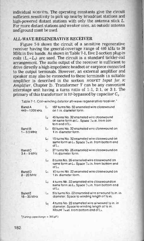
individual MOSFETS. The operating constants give the circuit sufficient sensitivity to pick up nearby broadcast stations and
high-powered distant stations with only the antenna stick L. For more distant stations and weaker ones, an outside antenna
andground must be used.
ALL -WAVE REGENERATIVE RECEIVER Figure 7-9 shows the circuit of a sensitive regenerative
receiver having the general -coverage range of 440 kHz to 30
MHz in five bands. As shown in Table 7-1, five 2 -section plug-in coils ( LI -L2) are used. The circuit is a standard tickler -coil
arrangement. The audio output of the receiver is sufficient to drive directly a high -impedance headset or earpiece connected
to the output terminals. However, an external amplifier and speaker may also be connected to these terminals ( a suitable
amplifier is described in the section MOSFET Input for Ic Amplifier, Chapter 2). Transformer T can be any convenient interstage unit having a turns ratio of 1:1, 2:1, or 3:1. The
primary of this transformer is RF-bypassed by capacitor C5.
Table 7-1. Coil -winding data for all -wave regenerative receiver.*
Band A L, 187 turns No. 32 enameled wire closewound 440-1200 kHz on 1 in. diameter form.
Band B 1-3.5 MHz
Band C 3.4-9 MHz
Band D 8-20 MHz
Band E 18-30 MHz
L2 45 turns No. 32 enameled wire closewound on same form as L,. Space 1/16 in. from bot-
tom end of L.,.
L, 65 turns No. 32 enameled wire closewound on 1 in. diameter form.
L2 15 turns No. 32 enameled wire closewound on same form as L,. Space 1/,6 in. from bottom end
of L,.
LI 27 turns No. 26 enameled wire closewound on 1 in.diameter form.
L2 8 turns No. 26 enameled wire closewound on same form as LI. Space 1/16in. from bottom end
of LI.
LI 10 turns No. 22 enameled wire closewound on 1 in. diameter form.
L2 4 turns No. 22 enameled wire closewound on same form as L,. Space 1/16 in. from bottom end oft,.
LI 5'/2 turns No. 22 enameled wire airwound 1/2 in. in diameter. Space to winding length of 1/2 in.
L2 4 turns No. 22 enameled wire airwound 1/2 in. in diameter. Space to winding length of 1/4 in.
Mount 1/16 in. from bottom end of LI.
(Tuning capacitance = 365 pF.)
182
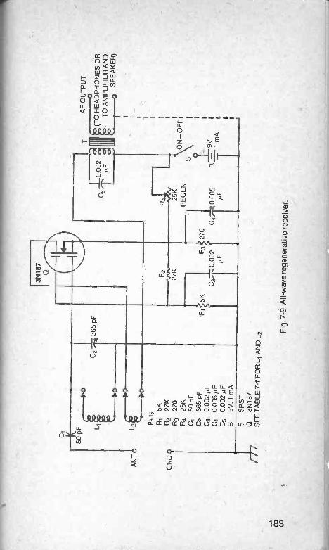
50 p
F
AN
T b
L2
0C
2 7-
4- 3
65 p
F
3N18
7
Par
ts
R1
5K
GN
D 0
R2
27K
R3
270
R4
25K
C1
50 p
FC
236
5 pF
C3
0.00
2 µF
C4
0.00
5µF
C5
0.00
2 µF
B9V
, 1 m
A
R2
27K
Ri
5K
-I-0
002
g/IF
1=1,
.!L25
KR
EG
EN
R3
270
C37
-7 0
.002
C4
- 0.
005
µF
AF
OU
TP
UT
(TO
HE
AD
PH
ON
ES
OR
TO
AM
PLI
FIE
R A
ND
SP
EA
KE
R)
\N-
OF
F
9V
T1
mA
///C
O
SS
PS
TQ
3N18
7S
EE
TA
BLE
7-1
FO
R L
i AN
D L
2 Fig
. 7-9
. All
-wav
e re
gene
rativ
e re
ceiv
er.

In this circuit, gate 1 of the MOSFET receives its negative bias from the voltage drop resulting from the flow of drain
current through RF-bypassed source resistor R3. The gate -2
electrode receives its positive bias from voltage divider R1-R2-R4. Current drain from the 9V supply is approximately
1 mA, but this may vary somewhat with individual mosFETs.
RF MIXER Figure 7-10 shows the circuit of a simple mixer
( converter) stage for radio -frequency applications. Such a stage is readily incorporated into the front end of a
superheterodyne receiver or test instrument. Here, the incoming signal (as from RF amplifier stage) is presented to
gate 1 of the MOSFET, while the local oscillator signal is applied to gate 2. The coupling capacitances, C1 and C2, will be
satisfactory in most cases. The IF transformer is selected for the desired intermediate frequency.
In this arrangement, the negative voltage resulting from the flow of drain current through source resistor R5 is too high for the gate -1 electrode of the MOSFET (the drain current has
been selected for the best transconductance, and source resistor R5 for optimum operation of the MOSFET). To
counteract this, a proper positive voltage, developed by voltage divider R3 -1i4 is also applied to gate 1, and the
resulting bias has the correct value. Gate 2 of the MOSFET
receives its positive bias from voltage divider R1-R2. With an individual MOSFET, resistance R2 in this divider may require
some adjustment for maximum conversion gain. Current drain from the 18V source in the receiver or test instrument is approximately 10 mA, but this may vary somewhat with individual MOSFETS.
TUNING METER Figure 7-11 shows the circuit of a sensitive tuning meter
which may be added to a receiver. The advantage of a MOSFET
in this setup is its high input resistance, which results in no discernible loading of the receiver's AGC system.
This circuit is similar to that of an electronic DC voltmeter. The indicating meter is connected in the drain circuit in a
4 -arm bridge circuit; the arms of this bridge consist of resistor R2, the two "halves" of potentiometer R3, and the internal
drain -to -source resistance of the MOSFET. With the receiver detuned from any station, potentiometer R3 is set to zero the
meter. Subsequently. the meter will be deflected upscale
184

OS
CIL
LAT
OR
INP
UT
6 8
pF
C2
SIG
NA
LIN
PU
Tll
250
pF
CO
MM
ON
>
CO 01
3N18
7O
R7-
70.0
02pF
R2
120K
11K
-A I'
a1
a'T L
-JI th
IF O
UT
PU
T
R3
100K
Ra
27K
Rs
330
0 00
2 p.
F
Fig
. 7-1
0. R
adio
-fr
eque
ncy
mix
er.
0.00
2
Par
ts
R1
11K
R2
120K
R3
100K
R4
27K
R5
330
C1
6.8
pFC
225
0 pF
C3
0.00
2µF
C4
0.00
2µF
C5
0.00
2µF
03N
187
TO
+18
V>
10 m
A

CO
Par
tsA
2
R1
10M
1KR
21K
F3
5K W
WM
0-50
DC
µA
3N18
7O
3N18
7O
TO
NE
GA
GC
BU
S
TO
GR
OU
ND
<
R1
10M
SE
NS
ITIV
ITY
0-50
DC
µA
Fk3
ZE
RO
SE
T
Fig
. 7-1
1. T
unin
g m
eter
.
5K W
W
>+
TO
DC
SU
PP
LY(6
V 1
1.2
mA
)

whenever a carrier is tuned in, and the deflection will beproportional to the signal strength. In terms of some referencesetting of the receiver gain controls, the scale of the metermay be calibrated in microvolts, millivolts, S -units, or otherindicators of signal strength. For establishing an S -meterscale, make 100 p,V equal to S9, 50 µV equal to S8, 25 µV to S7,etc. (Each S -unit should be equal to 6 dB voltage change.)
Current drain from the 6V supply in the receiver isapproximately 11.2 mA, but this may vary somewhat withindividual MOSFETS.
HETERODYNE ELIMINATORThe circuit shown in Fig. 7-12 is a highly effective one for
eliminating heterodyne whistles in a receiver that has noprovision, such as a crystal filter or Q -multiplier, for gettingrid of this annoyance. This circuit operates in the audiochannel of the receiver, which it does not load, owing to thehigh resistance of RI. The eliminator may be operated at theAF output of the receiver or patched into the audio channel.
The tuned section of the circuit is a Hall network(C3-C4-05 R3- R4) connected between the input and outputstages. The advantage of this network is the tuning it provideswith only one potentiometer ( R4) . When R4 is set to the properpoint, the network, acting as a bandstop filter, removes thewhistle at the corresponding frequency.
The Hall network works best with a low -impedancegenerator and low -impedance load, and this condition isapproximated by driving it with a MOSFET source follower (Q1)and following it with a bipolar common -emitter stage (Q2)which exhibits medium -resistance input. A high -impedanceheadset or earpiece may be connected directly to the outputterminals, or an amplifier and speaker may be operated fromthe output. ( A suitable amplifier is described in the sectionMOSFET Input for Ic Amplifier, Chapter 2. )
Current drain from the 6V supply is approximately 2.2 mA,but this may vary somewhat with individual MOSFETs andbipolar transistors.
FLEA -POWER "QRP" TRANSMITTERFigure 7-13 shows the circuit of a low -powered transmitter
suitable for clear -channel cw communication and for antennatuneup operations. It consists of a conventional, keyed crystaloscillator. The DC input power of this transmitter isapproximately 60 mW.
In this circuit, the crystal ( XTAL) is selected for thedesired operating frequency, and the coil set L1-L2 is also
187

03 'op
0.1
ki..F
AF
INP
UT
H1
1M VO
LUM
E
s\O
N-
OF
F
B6V
=. 2.
2 m
AC
250
/..1
.F
)R
3
180K C4
C5
E -
I0.
1 /IF
0.01
12.F
0.1
1.1.
F
Par
ts
R1
1M
PO
TR
4
Alit
TIO
NI5
7T
AP
ER
TU
NIN
G
R2
R3
R4
R6
R6
C1 C2
C3
C4
C5
C6
C7
2N27
1202
500
180K
5K A
UD
IO T
AP
ER
470
27K
0.1
/IF50
µF
0.1
µF
Rs
RS
27K
0.1
AF
AF
OU
TP
UT
(TO
HE
AD
PH
ON
ES
OR
TO
AM
PLI
FIE
RA
ND
SP
EA
KE
R)
470
C6
50 µ
F
0.01
/IF
B6V
, 2.2
MA
0.1
µFS
SP
ST
50µF
0.1
3N18
70.
1 p_
FQ
.2N
2712
Fig
. 7-1
2. H
eter
odyn
e el
imin
ator
.

Cl
25 p
F
3N18
7O
Imo,
XT
AL
I=1
/47
03
470K
R2
C2
,77-
-N
0.0
02
ILF
R3
5K W
W
10K
R4
47K
0 00
2 kL
F
RF
CE
2.5
mH
of
R5
3 9
M
iC3-
0 0
02 k
iF
Fig
. 7-1
3. F
lea
-pow
er tr
ansm
itter
.
L
C57
-za
50 p
FT
UN
ING
0-1
DC
mA KE
Y
L2
Par
ts
R1
470K
R2
10K
R3
5K W
WR
447
K
R5
3.9
C1
25 p
FC
20.
002µ
FC
30.
002µ
FC
40.
002µ
FC
550
pF
B6V
. 10.
1 m
AM
0-1
DC
mA
RF
C 2
.5 m
HO
3N18
7S
EE
TE
XT
FO
RL1
AN
D L
2
RF
OU
TP
UT

chosen for this frequency. Suitable end -link coil sets for use with the 50 pF tuning capacitor shown are commercially
available for the amateur bands. The use of shunt feed in the drain output circuit enables the tank L1-05to be grounded.
Tuning is simple and straightforward: With the key depressed and no load connected to the output terminals, C5 is
adjusted for minimum dip of drain current as indicated by milliammeter M. The load then is connected and adjusted to
raise the dipped current to 10 mA. Finally, the tuning is touched up, by readjustment of C5, for dip. (Some operators, as
is well known to the ham reader, prefer to detune slightly to one side of dip.)
The positive bias applied to gate 2 of the MOSFET may be adjusted by means of rheostat R3. This adjustment permits
maximum output to be obtained with an individual MOSFET. The current drain from the 6V supply B is approximately 10.1
mA, but this may vary somewhat with individual MOSFETh.
FREQUENCY DOUBLER Figure 7-14 shows the circuit of a conventional frequency
doubler for use in low -powered transmitters and adapted for MOSFET operation. This doubler may be used, for example, in
conjunction with the oscillator -type transmitter described in the preceding section.
In this circuit, in the conventional manner of doubler operation, the tank circuit C4 -L is tuned to twice the frequency of the signal applied to the input terminals. Suitable
end -link coil sets (L,-L2) for use with the 100 pF tuning capacitor shown are commercially available for the amateur
bands. The RF output may be either link coupled, as shown by the solid lines, or capacitively coupled by means of C5 and the
dotted lines. In this circuit, the MOSFET runs at drain -current pinchoff,
this condition being obtained by means of proper gate -1 and gate -2 biases. The net negative bias on gate 1 results from the
negative voltage drop across source resistor R5 and the positive output of voltage divider R1-R2, while the positive
bias on gate 2 results from the output of voltage divider R3-R4. Some adjustment of resistances R2 and R3 may be required with individual MOSFET. The doubler is fully driven by a 1.5V peak signal at the input terminals.
Tuning is simple and conventional: With switch S closed, the driving signal applied to the input terminals, and no load
connected to the output terminals, capacitor C4 is adjusted for minimum dip of drain current as indicated by milliammeter
M. The load then is connected and adjusted to raise the dipped
190

Par
ts
Ri
39K
C4
100
pFR
21
MC
s50
0 pF
R3
750K
C6
0,00
5 µF
R4
220K
B18
V, 1
0 m
AS
EE
TE
XT
FO
R L
i AN
D L
2R
527
0M
0-15
DC
mA
C1
500µ
FR
FC
2.5
mH
3N18
7
C2
0.00
5µF
SS
PS
TQ
C3
0.01
µF
03N
187
Ci
500
pF
RF
INP
UT
1 0R
FC
g2.
5 m
Hto
r
Li
I 2
C4
100
TU
NIN
GpF
C5
500
pF
0-15
DC
mA
R2
R3
1 M
750K
R1
39K
R4
220K
R5
C2
0.00
5-
270
0.01
1.1
F
\ON
- O
FF
-18
VB
- T10
mA
O OR
F O
UT
PU
T
C6
0.00
5 pi
F
/C
OF
ig. 7
-14.
Fre
quen
cy d
oubl
er.
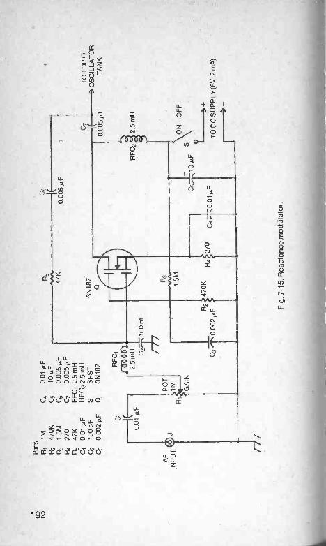
cDP
arts
Ri
1M04
0.01
µFR
247
0KC
s10
µFR
31.
5M06
0.00
5 p.
.F
R4
270
C7
0.00
5 p.
F.
R5
47K
RF
C1
2.5
mH
C1
0.01
i.k.
FR
FC
2 2.
5 m
H
C2
100
pFS
SP
ST
C3
0.00
2µF
03N
187
AF
INP
UT
0.01
;IF
R
PO
T1M G
AIN
RF
C1
0 0
0 C
IL,
2.5
mH C2-
100
pF
Rs
ovvv
47K
3N18
70
C6
0 00
5 µ.
F
R3
[0 0
05 p
.F
C7
aR
FC
2
1 5M
R2
470K
C3
0 00
2 µF
R4
270
0674
N-1
0 µF
0.01
µF
2.5
mH
Sp
\ON
- O
FF
TO
TO
P O
FO
SC
ILLA
TO
RT
AN
K
>+
TO
DC
SU
PP
LY (
6V, 2
mA
)
I/I
Fig
. 7-1
5. R
eact
ance
mod
ulat
or.

current to 10 mA. Finally, the tuning is touched up byreadjustment of C4 for dip. The DC power input of the doubler isapproximately 153 mW, but this may vary somewhat withindividual MOSFEIS.
REACTANCE MODULATORFigure 7-15 shows the circuit of a conventional reactance
modulator for frequency -modulating a self-excited oscillator.With the drain connected to the tank of the oscillator, thismodulator will swing the oscillator frequency proportionate tothe amplitude of the audio voltage applied at jack J. CapacitorC6 and resistor R5 provide the necessary phase shift to gate 1 ofthe MOSFET. The entire unit must be mounted close to theoscillator, so that the connection between C7, C6, and theoscillator tank may be as short and direct as practicable. Thisarrangement is suitable not only for FM transmitters, but forsweeping the frequency of a test oscillator.
In this circuit, the negative gate -1 bias is obtained from thevoltage drop resulting from the flow of drain current throughsource resistor R4, and the positive gate -2 bias from voltagedivider R2- R3. Current drain from a 6V supply in thetransmitter or test instrument is approximately 2 mA, but thismay vary with individual mosFurs.
193

Index
A
Ac null detector
RF relay voltmeter adapter
Active high-pass filter low-pass filter
probe Adapter
constant -current output ( dual -polarity) signal tracer
AF -actuated relay
mixer oscillator ( Colpitts) oscillator ( Franklin) oscillator ( Hartley) oscillator ( phase -shift) oscillator ( sun -powered) oscillator ( tickler feedback) oscillator ( Wein bridge)
oscillator) Villard )
/RF signal tracer signal tracer adapter
Acc amplifier Alarm, carrier -failure
All -wave regenerative receiver AM monitor
Amplification. gated Amplifier
bandstop ( Lc) current
DC DC galvanometer oc voltage
gated -off gated -on
headphone high -gain
high-pass ( Lc -tuned) IF ( double -tuned) IF ( single -tuned) Lc -tuned low-pass
paraphase peak
peaked response
162
83 157
44 40.42 157
170 113 157
87 31 120 122
117
124 128 116 126 128 154 157
27 105 179 166 35
52 61 60 64 62 38 35 56 20 44 77 74 40 33 46.49 56
push-pull RF 71
Hc-coupled 19 Hc-tuned low-pass 42
regenerative 77 RF 66
RF ( 100 MHz) 71
RF ( transmitter -type) 69 single -stage 18
slot ( notch ) 52.154 2 -stage ( high -gain) 22
with AGC 28 video 80
Amplitude modulation monitor 166 AND gate 105
Audio -actuated relay 87
mixer 31 Audio oscillator
col pitts 120 Franklin 122 Hartley 117
phase shift 124
sun -powered 128 tickler coil 116 villard 128
wien bridge) 126
B Balanced
DC voltmeter modulator
Band rejection amplifier Bandstop
amplifier) Lc) amplifier (}lc)
Bandwidth, rejection Base connections, MOSFET Bass cut
Bistable multivibrator Bridge, Wien
Broadcast -band coil data
receiver C
Capacitance measuring device
relay
147 174 52.154
52 54 52 15 44 172
126
62 179
151
98
194

Carrier -failure alarmCascadeCathode follower equivalentCenter -zero DC voltmeterChannel
N
1052225
149
11
-input audio mixer-MOSFET phase inverter-polarity DC voltmeter-polarity output adapter
E
3133
149113
Charge detectorChecker. Lc ( wide range)Code practice monitorCoincidence relayCoil data
12171
15716691
Earphone amplifierElectroscopeEliminator. heterodyneEmitter follower equivalentEnhancement mode
56171
1872513
broadcast band 62 Fshortwave bands
Colpittsaudio oscillatoroscillator ( RF self-excited)
Common -source amplifierConstant -current adapterConverter
impedance ( DC)RFsine to square
Crystal-controlled IF oscillatoroscillator ( Pierce )oscillator I standard I-type frequency standard
Currentamplifier circuitconstant
Cutoff. high -frequency 40.
179
12013418
170
113189163
144140138152
61170
44. 142
Failure, carrierFeedback. negativeFET
junctionVS MOSFET
Filterhigh-pass )active)low-pass ( active)
Flip-flopFloating gateFm reactance modulatorFollower
sourcesource I Dc I
Franklin audio oscillatorFrequency
doublerstandard. self-excited
10522
11
13
4442
17217
133'
2566
122
190149
Cw monitor 166 GD Gain. source follower 27
Dc Galvanometer amplifier (DC) 64
amplifier 60 Gategalvanometer amplifier 64 AND 105
relay ( zero current) 81 floating 17
signal invertersource follower
110
66
OR
-protected MOSFET11014
voltage amplifier 62 Gated -on amplifier 35
voltmeter 145 Gated -off amplifier 38
voltmeter ( balanced) 147 Generatorvoltmeter ( center zero) 149 audio ( tickler -type) 116
Degeneration 22 square -wave 163
Delay relay 100 tone ( Villard) 128
Delayed pull -in relay 100 tone) Wien bridge) 126
Depletion mode 12 HDemodulator, light beam 177, 179 Hall network 187Detection. null 46 Handling care. MOSFET 16Detector Hartley
charge 171 audio oscillator 117null (AC) 162 oscillator 77proximity 95 Headphone
Distortion reduction 22 amplifier 56Double -tuned IF amplifier 77 amplifier ( peaked) 56Doubler, frequency 190 HeatDual excessive 17
-gate MOSFET 12 -operated relay 95
195

Heterodyne eliminator High -gain amplifier
High-pass amplifier Hybrid amp with AGC
187 20 44 27
Modulation monitor Modulator
balanced reactance
Monitor
166
174
193
AM 166
IF amplifier CW 166
double -tuned 77 MOSFET
input stage 29 description 11
regenerative single -tuned
77 74
/bipolar amplifier gate -protected
28 14
IF oscillator. handling care 16
crystal 144 input circuit ( for is amp) 30 self-excited 44 mounting 16
IF/HF signal tracer Impedance converter ( DC)
155 113
polarities precautions
13
16
Inductance measuring device 162 structure 12
Input stage for ic amplifier Integrated diodes
29 14
symbols transconductance
13 13
Interval timer 100 vs junction FET 13
Intrusion relay 98 Mounting. MOSFET 16
Inverter Multiplier, frequency 190
DC signal 110 Multivibrator phase 33 bistable 172
drain -coupled 128
J
Junction FET 11 N
VS MOSFET 13 N -channel MOSFET 11
Negative feedback 22
L Network Hall 187
parallel -T 54 checker, wide -range 157 Noise relay 100 -tuned AF relay 87 Notch -tuned amplifier 40 amplifier ( Lc) 52 -tuned high-pass amplifier 44 amplifier ( Hc) 54 -tuned notch amplifier 52 Null -tuned peak amplifier 46 detection 46
Light detector. AC 162 -beam receiver 177 circuit 51
-operated relay 93 meter ( sensitive) 163 0
Logic AND circuit
OR gate Low
-pass amplifier -power transmitter
105 110
40 187
Off gating On gating OR gate
Oscillator AF ( sun -powered)
colpitts ( audio)
38 35 110
128 120
M crystal ( Pierce) crystal ( standard)
141
138 Meter /doubler 190
light 163 Franklin (audio) 122 tuning 184 Hartley 77 Miniature transmitter 187 Hartley ( audio) 117
Mixer 31 IF ( crystal) 144 RF 184 IF ( self-excited) 144 Mode,
depletion 12
multivibrator RF ( Colpitts self-excited)
128 134
enhancement 13 RF self-excited ( Hartley) 134
196
self-excited RF ( tickler) 128sun -powered (RI') 140tickler ( audio) 116villard 128wien bridge 126
Output adapter. dual -polarity 113
PP -channel MOSFETParallel -T networkParaphase amplifierPass
high-low -
Peak amplifierPeaked -response amplifierPhase
40.
12
5433
44424956
inverter 33-shift audio oscillator 124shifter, stepping 105shifter, variable 103
Photocelland relay 93demodulator 177. 179
Photoelectric relay 93Photographic light meter 163Pickup
stray 17
supersonic 174Pierce crystal oscillator 140Plate
relay 81Polarity. MOSFET 13Positive feedback 77Probe. active 157Proximity detector 98Pulse inverter 110Push-pull RF amplifier 71
QQ -multiplier simulator 187QRP transmitter 187
RReactance modulator 193Rc
-coupled amplifier circuit 19
-tuned AF oscillator 128-tuned AF relay 89-tuned high-pass amplifier 44-tuned high-pass circuit 46-tuned low-pass amplifier 42-tuned notch amplifier 54-tuned peak amplifier 49
Receiveral -wave 179broadcast 179light beam 177. 179
Reducing distortionRegenerative
IF amplifierreceiver (Bc)receiver ( sw)
Rejection bandwidthRelay
AC RF
audio -actuatedcapacitancecoincidenceheat -operatedlight -activatednoise -operatedRF ( sensitive)touch -platezero -current
Resistor, source ( unbypassed)RF
22
7717917952
838798919593
100859581
22
-actuated relay 83amplifier, general-purpose 66amplifier. 100 MHz 71amplifier, push-pull 71amplifier ( transmitter -type) 69coils ( winding data) 62colpitts oscillator ( self-excited)
134mixer 184oscillator, self-excited ( tickler)
128oscillator, sun -powered 140relay ( AC) 83self-excited oscillator 134/IF signal tracer 155
S
S -meterSelf-excited
colpitts RF oscillatorfrequency standardHartley RF oscillatorIF oscillator
SensitiverelayRF relay
ShieldingShifter
phasephase ( variable)
Sideband balanced modulatorSignal
absorption circuitgenerator. audio ( tickler coil)inverter. DCtracer adaptertracer. AF/RFtracer. IF/RF
Silicon wafer
184
134149134144
818517
33103114
49116110157154155
11
197

Sine - villard 128
to square -wave converter 163 wien bridge 126
wave AF oscillator 124 Touch -plate relay 95
Single -
Tracer ended RF amplifier 70 signal (AF/RF) 154
gate MOSFET 12 signal (IF/RF) 155
stage amplifier 18 Transconductance. MOSFET 13
tuned IF amplifier 74 Transmitter Slot low -power 187
amplifier ( Lc) 52 RF amplifier 69
amplifier ( RC) 54 Treble cut 42
Solar -
Tuned RF/IF tracer 155
powered audio oscillator 128 Tuning meter 184
powered RF oscillator 140 Two - Sound switch 100 input audio mixer 31
Source follower 25 MOSFET phase inverter 33
DC 66 stage amplifier ( high -gain) 22
Square -wave generator 163
Standard U crystal oscillator
frequency ( self-excited) 138 140
Unbypassed source resistor 22
Static -charge detector Step -type phase shifter
Stray pickup Strength meter (RF)
Suboscillatory amplifier Sun -powered
audio oscillator
171
105 17
184 77
128
V
Variable phase shifter VHF RF amplifier
Video amplifier circuit
Villard audio oscillator
103 71 50 79 128
RF oscillator Superheterodyne converter
Supersonic pickup Switch. sound
140 184
174 100
Voltage amplifier. Dc
gain, source follower Voltmeter
62 27
adapter ( Ac) 157
T booster
DC
50 145
Tapped -
DC center -zero) 149
capacitance AF oscillator 120 inductance AF oscillator
capacitance self-excited oscillator
Temperature -sensitive relay Thermal relay Tickler -coil oscillator ( AF)
Timer, interval Time delay relay
117
134 95 45 116 100 100
w Wafer. silicon
Wideband amplifier
video amplifier circuit Wien bridge AF oscillator
Winding of coils
11
80 79 126 62
Tone generator colpitts 120
Hartley 117 Zeners in FET gates 14
Franklin 122 Zero -
tickler -type 116 center meter 64
198

Getting Started With Transistors, 160 p., 90 ill., . No. 116, $3.95
New IC FET Principles 8 Projects, 154 p., 60 ill. No. 613, $3.95
Semiconductors from A to Z, 272 p., over 300 ill., No. 493, 55.95
Transistor Circuit Guidebook, 124 p., 118 ill., No. 470, 54.95
Transistor Circuits, 160 p., 144 ill., No. 63, 54.95
Transistor Techniques, 96 p., 76 ill., No. 61, 53.95
Transistor Theory for Technicians 8 Engineers, 224 p., No. 717, 55.95
Transistors -How to Test, How to Build, 96 p., 65 ill., No. 94, $2.95
Transistors --Theory 8 Practice, 160 p., 138 ill., No. 75, $3.95
Understanding Solid -State Circuits, 192 p., 140 ill., No. 513, $4.95
Working With Semicondcutors, 224 p., 185 ill., ....No. 501, $4.95
Amat. Filmmaker's H'book Sound Sync 8 Scoring, No. 736, 55.95
Complete Handbook of Home Painting, 210 p., 96 ill., No. 762, 54.95
Electronic Experimenter's Guidebook, 182 p., 86 ill., No. 540, $4.95
Electronic Hobbyist's IC Project H'book, 154 p., No. 464, 54.95
Electronics for Shutterbugs, 204 p., 109 ill., No. 679, 55.95
Electronics Self -Tough With Experiments 8 Projects, No. 553, 55.95
Fun With Electricity, 128 p., No. 83, $3.95
Handbook of IC Circuit Projects, 224 p., 134 ill. No 619, $4.95
Landsailing... from RC Models to the Big Ones, No. 659, 54.95
Miniature Projects For Electronic Hobbyists, 168 p., No. 667, 53.95
Model Car Racing by Radio Control, 224 p., 250 ill., No. 592, 53.95
Model Radio Control, 192 p., 192 ill., No. 74, $4.95
Model Sail 8 Power Boating...by Remote Control, No. 693, 54.95
New Skill -Building Transistor Projects 8 Exper., No. 129, 54.95
104 Easy Transistor Projects You Can Build, 224 p., No. 462, 54.95
Practical Circuit Design for the Experimenter, 196 p., No. 726, 54.95
Practical Triac/SCR Projects for the Experimenter, .. No. 695, $4.95Professional Picture Framing for the Amateur, 168 p., No. 674, $3.95
Radio Control Handbook -3rd Ed., 320 p., 238 ill., No. 93, $6.95
Radio Control Manual -2nd Ed., 192 p., 158 ill., No. 135, 54.95
Radio -Electronics Hobby Projects, 192 p., 214 ill., ..14o. 571, $4.95
64 Hobby Projects for Home 8 Car, 192 p., No. 487, 54.95
Solid -State Circuits Guidebook. 252 p., 227 ill., No. 699, 55.95
Solid -State Projects for the Experimenter, 224 p., No. 591, $4.95
Stereo/Quad Hi Fi Principles 8 Projects, 192 p., No. 647, 54.95
Transistor Projects for Hobbyists 8 Students, 192 p., No. 542, 54.95
Acoustic Techniques for Home 8 Studio, 224 p., No. 646, 54.95
Cassette Tape Recorders. 204 p., 171 ill., No. 689, 54.95
Electronic Music Production, 156 p., 79 ill. No. 718, 53.95
Electronic Musical Instruments, 192 p., 121 ill., No. 546, 54.95
Experimenting With Electronic Music, 180 p., 103 ill ,'No. 666, 54.95
4 -Channel Stereo-From Source to Sound -2nd Ed., No. 756, 54.95
Handbook of Magnetic Recording, 224 p., 90 ill. No. 529, 54.95
Hi-Fi for the Enthusiast, 176 p., 51 ill., No. 596, $3.95
How to Build Solid -State Audio Circuits, 320 p., No. 606, 55.95
Installing 8 Servicing Home Audio Systems, 256 p., No. 505, 55.95
Pictorial Guide to Tape Recorder Repairs, 256 p.,.. No. 632, 54.95
Questions 8 Answers About Tope Recording, 264 p., No. 681, 55.95
Selecting 8 Improving Your Hi-Fi System, 224p. No. 640, 54.95
Servicing Cassette 8 Cartridge Tape Players, 294 p., No. 716, 56.95
Servicing Electronic Organs, 196 p., No. 503, $7.95
Servicing Modern Hi-Fi Stereo Systems, 248 p., No. 534, 54.95
Tape Recording for Fun 8 Profit, 224 p., 200 ill., No. 497, 55.95
Advanced Applications for Pocket Calculators, 308 p., No. 824, 55.95
Beginner's Guide to Computer Logic, 192 p., 100111., No. 548, 54.95
Beginner's Guide to Computer Programming, 480 p., No. 574, 56.95
Computer Circuits 8 How They Work, 192 p., No. 538, $4.95
Computer Technician's Handbook, 480 p., 400 ill., No. 554, 58.95
Getting the Most Out of Your Electronic Calculator, No. 724, 54.95
Simplified Computer Programming The RPG Way, No. 676, 55.95
CB Radio Operator's Guide, 224 p., scores of ill
Citizens Band Radio Service Manual, 228 p.,
Complete f M 2 -Way Radio Handbook, 294 p.
Complete Shortwave Listener's "torkicok, 288 p., .. No. 685, 56.95
Ham Rodio Incentive Licensing Guide, 160 p., 29 ill., No. 469, 53.95
How To Be A Ham --Including Latest FCC Rules, ....No. 673, $3.95Marine Electronics Handbook, 192 p., 106 ill., No. 638, $4.95
Mobile Radio Handbook, 192 p., 175 ill., No. 665,54.95
Modern Communications Switching Systems, 276 p., No. 678, 517.95
104 Ham Radio Projects for Novice 8 Technician, No. 468, 53.95
Pictorial Guide to CB Radio Installation 8 Repair, No. 683, 55.95
RTTY Handbook, 320 p., 230 111 , No. 597, $6.95
The 2 -Meter FM Repeater Circuits Handbook, 312 p., No. 621, 56.95
Amateur FM Conversion 8 Construction Projects, No. 722, 55.95
Amateur Radio Advanced License Study Guide -2nd Ed , No. 827, 55.95
Amateur Radio Extra -Class License Study Guide, No. 543, 54.95
Amateur Rodio General License Study Guide -2nd Ed , No. 851, 57.95
Amatuer Radio Novice License Study Guide -2nd Ed., No. 873, 55.95
Broadcast Announcer 3rd Class FCC Study Guide No. 704, 53.95
No. 499, $5.95
No, 581, $5.95
No. 735, $6.95
Basic Audio Systems, 140 p., 203 ill., No. 634, 54.95
Basic Color Television Course, 420 p., over 300 ill., No. 601, 57.95
Basic Digital Electriariics, 210 p., 117 ill., Ho. 728, $4.95
Basic Electricity 8 Beginning Electronics, 252 p., No. 628, 55.95
Basic Electronic Circuits Simplified, 352 p., 170 ill., No. 622, 55.95
Basic Electronic Test Procedures, 416 p., 178 ill., No. 627, 56.95
Basic Electronics Course, 384 p., 275 ill., No. 588, $6.95
Basic Math Course for Electronics, 168 p. No. G100, $4.95
Basic Radio Course, 224 illustrated p., No. 104, 55.95
Basic Transistor Course, 224 p., pocked with ill., No. 111, $4.95
Basic TV Course, 224 p., 128 ill. No. 105, 55.95
Commercial FCC License Handbook, 44 p., 150 ill., No. 582,
Dictionary of Electronics 420 p., 487 ill., No. 300, 54.95
Digital Electronics: Principles 8 Practice, 288 p., No. 585, 55.95
Electrical Wiring 8 Lighting For Home 8 Office, . No. 671, $4.95
Electronics Unraveled A Commonsense Approach, . No, 691, $4.95
How to Read Electronic Circuit Diagrams, 192 p.,.. No. 510, 54.95
Industrial Electronics: Principles 8 Practice, 416 p., No. 583, $8.95
Introduction to Medical Electronics, 271 p., 126 ill., No. 630, $6.95
Modern Radar-Theory, Operation, and Maintenance, No. 575, 57.95
Pulse 8 Switching Circuits, 256 p., 184 ill., No. 528, $5.95
Connecting Diagrams for Induction Motors, 132 p., No. 96, 55.95
Electric Motor Repair Shop Problems 8 Solutions, No. T4, $10.95
Electric Motor Test 8 Repair, 160 p No. 97, 56.95
How to Repair Home 8 Auto Air Conditioners, No. 520, 54.95
Major Appliance Repair Guide, 288 p., No. 555, 55.95
Refrigeration, 160 p., 53 ill., No. 295, 53.95
Small Appliance Repair Guide-Vol. 1, 224 p., No. 515, 54.95
Small Appliance Repair Guide-Vol. 2, 210 p., . No. 715, $4.95
The Home Appliance Clinic; 196 p., 61 ill, No. 745, $4.95
Auto Electronics Simplified, 256 p., 202 ill., No. 749, 55.95
Complete Auto Electric Handbook, 210 p., 139 ill., . No. 748, 55.95
Complete Guide to Outboard Motor Sere. 8 Repair, No. 727, 56.95
Complete Handbook of Auto Engines 8 Systems, No. 734, 55.95
Complete Handbook of Lawnmower Repair, 434 p., No. 767, 57.95
Complete Mini -Bike Handbook, 320 p., 145 ill., . No. 651, $5.95
Complete Snowmobile Repair Handbook, 350 p., . No. 705, 56.95
Everyman's Guide to Auto Maintenance, 191 p., .. No. 648, 54.95
How to Repair Small Gasoline Engines, 288 p., .. No. 617 55.95
Modern Auto Tuneup 8 Emission -Control Sorcg., No. 688, 55.95
Rapid Auto Tuneup 8 Troubleshooting, 192 p., 97 ill., No. 707, 53.95
Using Electronic Testers for Automotive Tune -Up No. 604, 54.95
C act for 6`r-f-'crftltagr: Oc'ff ago titte4= sn ffootiritv