exp.no.3.13 dc amplifier-gainstpius.ac.in/crm/assets/download/practical_paper-3... ·...
TRANSCRIPT
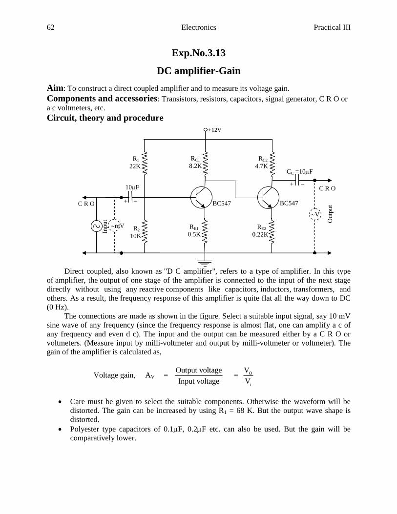
62 Electronics Practical III
Exp.No.3.13
DC amplifier-Gain
Aim: To construct a direct coupled amplifier and to measure its voltage gain.
Components and accessories: Transistors, resistors, capacitors, signal generator, C R O or
a c voltmeters, etc.
Circuit, theory and procedure
Direct coupled, also known as "D C amplifier", refers to a type of amplifier. In this type
of amplifier, the output of one stage of the amplifier is connected to the input of the next stage
directly without using any reactive components like capacitors, inductors, transformers, and
others. As a result, the frequency response of this amplifier is quite flat all the way down to DC
(0 Hz).
The connections are made as shown in the figure. Select a suitable input signal, say 10 mV
sine wave of any frequency (since the frequency response is almost flat, one can amplify a c of
any frequency and even d c). The input and the output can be measured either by a C R O or
voltmeters. (Measure input by milli-voltmeter and output by milli-voltmeter or voltmeter). The
gain of the amplifier is calculated as,
Voltage gain, AV = Output voltage
Input voltage = O
i
V
V
Care must be given to select the suitable components. Otherwise the waveform will be
distorted. The gain can be increased by using R1 = 68 K. But the output wave shape is
distorted.
Polyester type capacitors of 0.1F, 0.2F etc. can also be used. But the gain will be
comparatively lower.
mV
V
C R O
+12V
RE1
0.5K
10F
BC547
Inp
ut Ou
tpu
t
R1
22K
RC1
8.2K
R2
10K
RE2
0.22K
+
BC547
RC2
4.7K
CC =10F
+
C R O

Practical-III M C T 63
Observation and tabulation
Observation using C R O
Mean ………..
*Observation using a c voltmeters
Input peak voltage VP
mV r m s a c input
mV
r m s a c output
mV Gain O
V
i
VA
V
10 7.07
20 14.1
30 21.2
40 28.3
50 35.4
Mean ……………
Result The direct coupled amplifier is constructed and its voltage gain is determined.
Mean voltage gain of the amplifier AV = ……….
Peak
voltage
VP
mV
No. of divisions
corresponding to
input peak to
peak
Volt per
division
of input
mV
Input
Voltage
Vi mV
No. of divisions
corresponding to
output peak to
peak
Volt per
division
of output
volt
Output
Voltage
VO volt
Gain
OV
i
VA
V
10
20
30
40
50

64 Electronics Practical III
Exp.No.3.14
Feedback circuits-voltage series and current series
Aim: To construct voltage series and current series feedback circuits and study their
performance by comparing them with an amplifier without feedback.
Components and accessories required: BC547 (or, BC107) transistor, resistors,
capacitors (1 electrolytic 100 F and 2 polyester type 0.1F), power supply, C R O or d c
voltmeter, signal generator, etc.
Circuit, theory and procedure
If a part of the amplifier output is fed
back to the input of an amplifier it is known
as a feedback amplifier. There is a
significant change in the performance of the
amplifier when feedback is given. If the
feedback is in same phase of the input it is
called positive feedback and if the feedback
is out of phase with the input it is called
negative feedback. The resulting amplifiers
are known as positive feedback amplifiers
and negative feedback amplifiers.
There are, in general, four types of
feedback circuits, voltage series feedback,
voltage shunt feedback, current series
feedback and current shunt feedback. Now
we study only the voltage series feedback
and current series feedback circuits.
We first construct a common emitter
amplifier without feedback as shown in fig.a
and find out its gain for different inputs and
different loads. Then we convert this
amplifier into voltage series feedback
amplifier and current series feedback
amplifier by removing the emitter bypass
capacitor CE.
Current series feedback circuit: Fig.b
represents the circuit of a current series
feedback circuit. The input and the output
are measured by a C R O for different
values of input and load resistance. Voltage
gain is calculated in each case and compares
the result with that of the amplifier without
feedback.
C R O
+12V
C R O
RE
1K
0.1F
0.1F
CE =
10
0
F
+
BC547
Inp
ut
Ou
tpu
t
R1
68K
RC
4.7K
R2
10K
RL
Fig.a: Amplifier without feedback
C R O
+12V
C R O
RE
1K
0.1F
0.1F
BC547
Inp
ut
Ou
tpu
t
R1
68K
RC
4.7K
R2
10K
RL
Fig.b: Current series feedback circuit

Practical-III M C T 65
Voltage series feedback circuit (emitter
follower or voltage follower): The voltage
series feedback circuit is shown in fig.c. In this
case the output is same as the input. Thus the
circuit is also known as emitter follower or
voltage follower. The input and the output are
measured by a C R O for different values of
input and load resistance. Voltage gain is
calculated in each case and compares the result
with that of the amplifier without feedback.
Select the range of input voltages for
which there is no clipping of output.
Select one of the frequencies for
which the gain is maximum.
If the transistor is changed there may
be changes in values of other
components.
Observation and tabulation Frequency of the input = ………..Hz
RL
ohm
Vin
mV
Output voltage VO in mV Gain = VO/Vin
without
feedback
Current
series
feedback
Voltage
series
feedback
without
feedback
Current
series
feedback
Voltage
series
feedback
100K
10
20
30
68K
10
20
30
33K
10
20
30
10K
10
20
30
1K
10
20
30
330
10
20
30
Result Voltage series and current series feedback circuits are constructed and their performances
are studied by comparing them with an amplifier without feedback.
C R O
+12V
C R O
RE
1K
0.1F
0.1F
BC547
Inp
ut
Ou
tpu
t
R1
68K
RC
4.7K
R2
10K RL
Fig.c: Voltage series feedback circuit

66 Electronics Practical III
Exp.No.3.15
Hartley Oscillator using Transistor
Aim: To construct a Hartley oscillator and measure its frequency using a C R O.
Components and accessories required: Transistor, resistors, capacitors, inductors,
power supply, C R O, etc.
Circuit, theory and procedure
An electronic oscillator is an
electronic circuit that converts d c
energy into a c energy. It is essentially
an amplifier in which a part of the
output is fed back in phase to the
input. To maintain steady oscillations
the feedback circuit must satisfy the
Barkhausen criterion for oscillation,
which is,
(a) The feedback factor or loop
gain A = 1, where A is the
gain without feedback.
(b) The feedback should be
positive.
Fig.a shows the circuit of a
Hartley oscillator. In this oscillator,
the feedback is supplied inductively. The frequency of oscillation is frequency of the tank circuit
and is given by,
f = 1
2π LC, where, L L1 + L2
The circuit is soldered out in a board as shown in the fig.a. The output is measured by a C
R O. If T is the time period of the oscillation, then frequency of oscillation is given by,
f = 1
T
The time period can be determined as follows. The time base of C R O is adjusted such that the
wave is seen clearly. Measure the number of divisions of the horizontal scale in the C R O screen
in between two adjacent points with same phase-length of a wave- (distance between two
adjacent negative peaks or positive peaks). Let it be ‘x’. Then the time period T is obtained by
multiplying ‘x’ with time per division of the time base. T = ‘x’ divisiontime per division
L1, L2 and C are measured by an L-C-R meter. The experiment may be repeated for different
values of C, L1 and L2.
C R O
+12V
RE
1K
0.1F
0.1F
CE =
10
0
F
+
BC547
Ou
tpu
t
R1
68K
RC
4.7K
R2
10K
Fig.a: Hartley oscillator
L2=
20
mH
C
L1=
20
0m
H
R
33
0
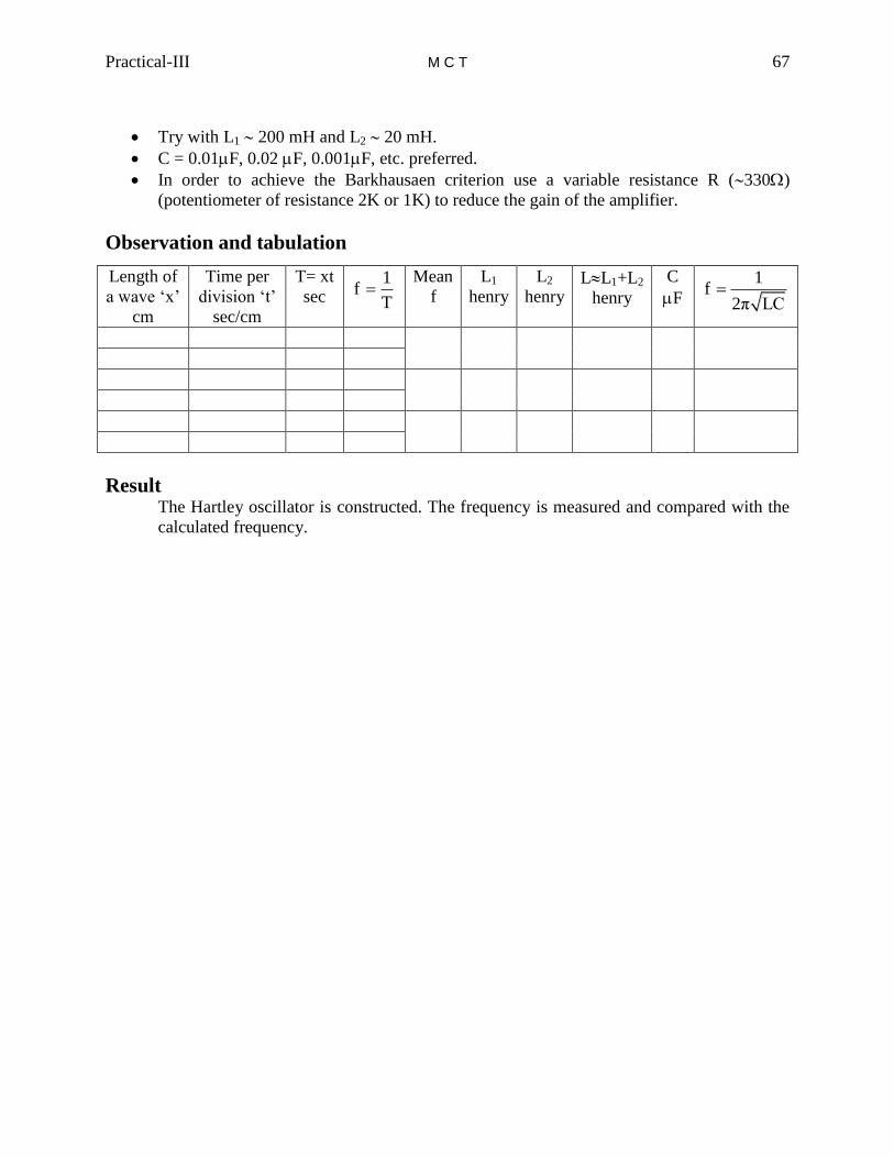
Practical-III M C T 67
Try with L1 200 mH and L2 20 mH.
C = 0.01F, 0.02 F, 0.001F, etc. preferred.
In order to achieve the Barkhausaen criterion use a variable resistance R (330)
(potentiometer of resistance 2K or 1K) to reduce the gain of the amplifier.
Observation and tabulation
Length of
a wave ‘x’
cm
Time per
division ‘t’
sec/cm
T= xt
sec 1
fT
Mean
f
L1
henry
L2
henry LL1+L2
henry
C
F
1f
2π LC
Result The Hartley oscillator is constructed. The frequency is measured and compared with the
calculated frequency.

68 Electronics Practical III
Exp.No.3.16
Colpitt’s Oscillator using Transistor
Aim: To construct a Colpitts oscillator and measure its frequency using a C R O.
Components and accessories required: Transistor, resistors, capacitors, inductors,
power supply, C R O, etc.
Circuit, theory and procedure
Colpitts Oscillator is also an
electronic circuit that converts d c
energy into a c energy. It is essentially
an amplifier in which a part of the
output is fed back in phase to the input.
Fig.a shows the circuit of a
Colpitts oscillator. In this oscillator, the
feedback is supplied capacitatively. The
frequency of oscillation is frequency of
the tank circuit and is given by,
f = 1
2π LC,
where, C = 1 2
1 2
C C
C C
The circuit is soldered out in a
board as shown in the figure. The output is measured by a C R O. If T is the time period of the
oscillation, then frequency of oscillation is given by,
f = 1
T
The time period can be determined as follows. The time base of C R O is adjusted such that the
wave is seen clearly. Measure the number of divisions of the horizontal scale in the C R O screen
in between two adjacent points with same phase-length of a wave- (distance between two
adjacent negative peaks or positive peaks). Let it be ‘x’. Then the time period T is obtained by
multiplying ‘x’ with time per division of the time base. T = ‘x’ divisiontime per division
L and C are measured by a L-C-R meter. The experiment may be repeated for different values of
L, C1 and C2.
L in the range of less than ~2 mH preferred.
C1 = 0.01F, 0.02 F, etc. and C2 = 0.01F, 0.02 F, etc. preferred.
In order to achieve the Barkhausaen criterion use a variable large resistance
(potentiometer of large resistance) in series with the feedback circuit to reduce the gain of
the amplifier.
C R O
+12V
RE
1K
0.1F
0.1F
CE =
10
0
F
+
BC547
Ou
tpu
t
R1
68K
RC
4.7K
R2
10K
Fig.a: Colpitts oscillator
C2
C1
L
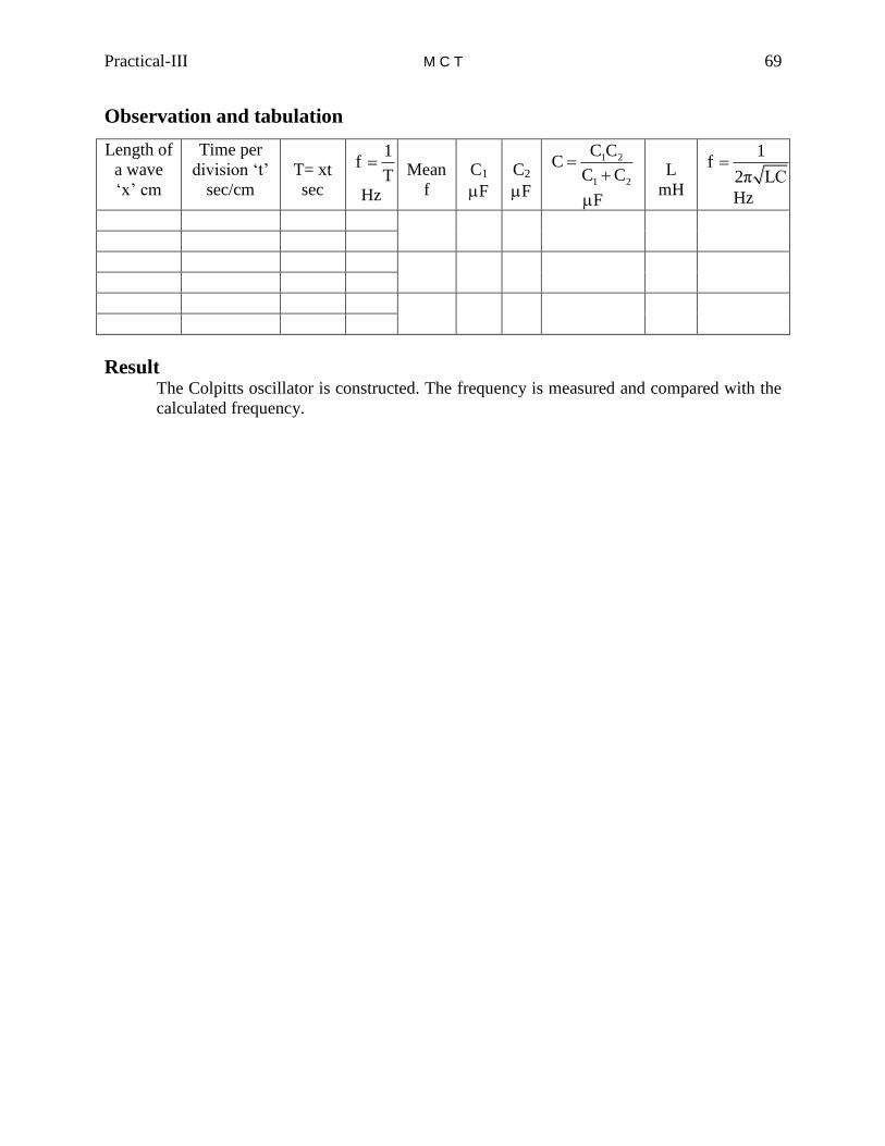
Practical-III M C T 69
Observation and tabulation
Length of
a wave
‘x’ cm
Time per
division ‘t’
sec/cm
T= xt
sec
1f
T
Hz
Mean
f
C1
F
C2
F
1 2
1 2
C CC
C C
F
L
mH
1f
2π LC
Hz
Result The Colpitts oscillator is constructed. The frequency is measured and compared with the
calculated frequency.

70 Electronics Practical III
Exp.No.3.17
Phase shift Oscillator using Transistor
Aim: To construct a phase shift oscillator and measure its frequency using a C R O.
Components and accessories required: Transistor, resistors, capacitors, inductors,
power supply, C R O, etc.
Circuit, theory and procedure
Phase shift oscillator is an oscillator with R-C feedback network. No inductor is used in the
circuit. This oscillator provides pure sine wave output. They are well suited for frequencies less
than 10 KHz.
The value of oscillations in
the circuit can be theoretically
calculated as,
f = 1
2πRC 6
The circuit is soldered out
in a board as shown in the
figure. The output can be
observed by a C R O. If T is the
time period of the oscillation,
then frequency of oscillation is
given by,
f = 1
T
The time period can be
determined as follows. The time
base of C R O is adjusted such that the wave is seen clearly. Measure the number of divisions of
the horizontal scale in the C R O screen in between two adjacent points with same phase-length
of a wave- (distance between two adjacent negative peaks or positive peaks). Let it be ‘x’. Then
the time period T is obtained by multiplying ‘x’ with time per division of the time base. T = ‘x’ divisiontime per division
The experiment may be repeated for different R-C combinations.
R = 2K3K. 2K is preferred.
C = 10 nF, 20 nF, 30 nF, etc. upto 1000 nF possible.
It is found that, according to Barkhausen criterion, the feedback fraction is 1/29. So to
obtain oscillations, the gain of the amplifier is greater than 29.
C R O
+12V
RE
1K
0.1F
0.1F
CE =
10
0
F
+
BC547
Ou
tpu
t
R1
68K
RC
4.7K
R2
10K
Fig.a: Phase shift oscillator
C C C
R R R

Practical-III M C T 71
Observation and tabulation
Length of
a wave
‘x’ cm
Time per
division ‘t’
sec/cm
T= xt
sec
1f
T
Hz
Mean
f
R
C
F
1f
2πRC 6
Hz
Result The phase shift oscillator is constructed. The frequency is measured and compared with
the theoretical frequency.

72 Electronics Practical III
Exp. No.3.18
Multivibrator- using Transistors
Aim: To construct an astable multivibrator using a bipolar junction transistor and measure its
frequency.
Components and accessories required: Transistors, resistors, capacitors, power supply,
C R O, etc.
Circuit, theory and procedure
Multivibrators are basically two stage
amplifiers with positive feedback from the
output of one of the amplifiers to the other.
These devices are very useful as pulse
generating, storing and counting circuits.
There are three basic types of multivibrators,
(1) astable multivibrators (free running), (2)
monostable multivibrators and (3) bistable
multivibrators.
Fig.a shows the circuit of an astable
multivibrator. It has no stable state, but has
only two quasi-stable states. Fig.b shows the
output of such an astable multivibrator.
The switching times of the two transistors can be calculated as,
T1 = 0.69Rb1C2
T2 = 0.69Rb2C1
Hence the time period of the wave is,
T = T1 + T2 = b1 2 b2 10.69 R C R C
Frequency, f = b1 2 b2 1
1
0.69 R C R C
If b1 b2R R R and C1 = C2 = C
T = 1.38RC
Frequency, f = 1
T =
0.725
RC
C R O
+12V
0.01F 0.01F
BC547
Ou
tpu
t
Rb2
270K
RC1
1.2K
0.02F
RC2
1.2K
Rb1
270K
C1 C2
BC547
Fig.a: Astable multivibrator
T1 T2
Fig.b: Output of an astable multivibrator

Practical-III M C T 73
The circuit is soldered out in a board and the time period is measured using a C R O. Calculate
the frequency of the wave. Repeat the experiment for different values of C.
To ensure oscillations, the value of the transistors must satisfy the conditions that,
1 b1
c1
R
R and 2 b2
c2
R
R
If 1 = 2 = , Rb1 = Rb2 = Rb and Rc1 = Rc2 = Rc, then the condition becomes
b
c
R
R
So select Rb and Rc such that the above condition must be satisfied.
For BC547 transistors Rb = 270 K and Rc = 1.2 K preferred
Use capacitors C1 and C2 in the range of values from 0.02 nF to about 50 nF.
Observation and tabulation
Length of
a wave
‘x’ cm
Time per
division ‘t’
sec/cm
T= xt
sec
1f
T
Hz
Mean
f
R
C
F
0.725f
RC Hz
Result The multivibrator is constructed. The frequency is measured and compared with the
theoretical frequency.

74 Electronics Practical III
Exp.No.3.19
Multivibrator- using IC555
Aim: To construct an astable and monostable multivibrator using the timer IC555 and study
their performance.
Components and accessories required: Timer IC555, pillar tag board, resistors,
capacitors, power supply, C R O, etc.
Circuit, theory and procedure
555 is an analog IC designed in 1971 by Hans Camenzind. It is a combination of linear
comparators and digital flip-flops. The standard 555 package includes 25 transistors, 2 diodes
and 15 resistors on a silicon chip installed in an 8-pin mini dual-in-line package. They are mainly
used for the construction of astable and monostable multivibrators.
Astable multivibrator
For an astable multivibrator, the connections are soldered on a pillar tag board as shown in
fig.c. The output obtained from the pin 3 is observed by a C R O and the frequency is
determined. Now we check whether the result obtained agrees with the theoretical value given as
VCC
DIS
(Discharge)
THR
(Threshold)
CTRL
(control voltage)
Ground
Trigger
(input)
Output
Reset
1
2
3
4
6
7
8
5 2 3
4
8
1
Fig.a: 555 timer IC
Fig.b : Pinout diagram of 555
+5V
C R O
1
2
3
4
6
7
8
5
Fig.c : Astable multivibrator with IC 555
CA
0.1F
0.1F
RA
1.5 K
RB
4.7 K
+4 to+15V
+5V
C R O
1
2
3
4
6
7
8
5
Fig.d : Monostable multivibrator with IC 555
0.1F
+4 to+15V
Trigger
RA
5.6 K
CA
0.1F
+

Practical-III M C T 75
follows. The time interval for which the output is high is given by, Thigh = A B Aln 2 R R C
and that for which it is low is given by, Tlow = B Aln 2 R C . Thus the total time interval,
T = Thigh + Tlow = A B Aln 2 R 2R C = A B A0.693 R 2R C
Frequency f = 1
T =
A B A
1
0.693 R 2R C
Monostable multivibrator Connections are soldered on
the pillar tag board as shown in
the fig.d. The square wave from a
C R O is given to the pin number
2 as the trigger input. The output
is observed by a C R O and the
frequency is measured.
The time interval for which
the output remains high in this case is, Thigh = 1.1RACA. Compare this with the observed value.
Measure Thigh and Tlow. Then the,
Frequency, f = 1
T =
high low
1
T T
Positive of trigger may also be given to pin 2, then negative is to be grounded.
Trigger input peak to peak voltage is sufficiently large (of the order of 10 volt).
Change the trigger frequency (lower than the output) till the Thigh of the output remains
constant.
Observation and tabulation
Astable Multivibrator
RA
K
RB
K
CA
F
Thigh
second
Tlow
second
Observed
T=Thigh+Tlow
second
Calculated, T = Thigh+Tlow
= A B A0.693 R 2R C
second
1f
T
Hz
Monostable Multivibrator
RA
K
CA
F
Calculated
high A AT 1.1R C second
Observed
Thigh
second
Observed
Tlow
second
Observed
T=Thigh+Tlow
second
1f
T Hz
Result Astable and monostable multivibrators are constructed with IC555 and their frequencies
are measured and compared with the theoretical values.
Tlow Thigh
Fig.e : Output of IC 555
76 Electronics Practical III
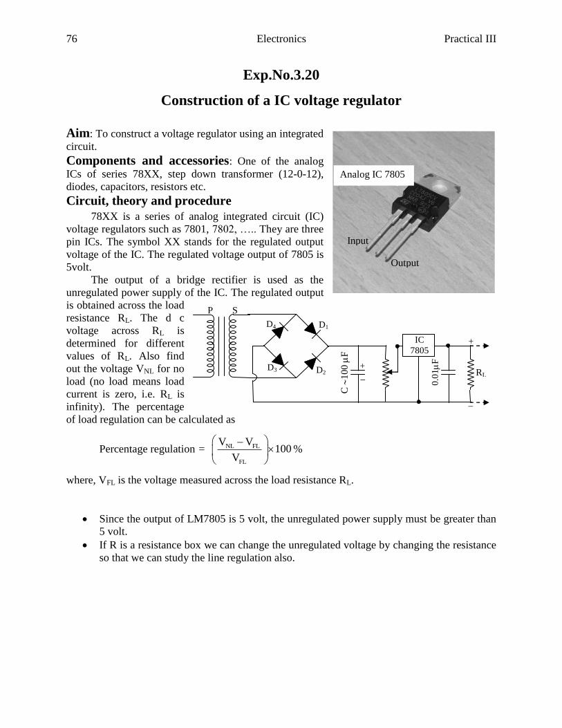
Exp.No.3.20
Construction of a IC voltage regulator
Aim: To construct a voltage regulator using an integrated
circuit.
Components and accessories: One of the analog
ICs of series 78XX, step down transformer (12-0-12),
diodes, capacitors, resistors etc.
Circuit, theory and procedure
78XX is a series of analog integrated circuit (IC)
voltage regulators such as 7801, 7802, ….. They are three
pin ICs. The symbol XX stands for the regulated output
voltage of the IC. The regulated voltage output of 7805 is
5volt.
The output of a bridge rectifier is used as the
unregulated power supply of the IC. The regulated output
is obtained across the load
resistance RL. The d c
voltage across RL is
determined for different
values of RL. Also find
out the voltage VNL for no
load (no load means load
current is zero, i.e. RL is
infinity). The percentage
of load regulation can be calculated as
Percentage regulation = NL FL
FL
V V100
V
%
where, VFL is the voltage measured across the load resistance RL.
Since the output of LM7805 is 5 volt, the unregulated power supply must be greater than
5 volt.
If R is a resistance box we can change the unregulated voltage by changing the resistance
so that we can study the line regulation also.
+
S P
D2
D4
D3
D1
+
C
100
F
IC
7805
RL
0.0
1
F
Analog IC 7805
Input
Output
Practical-III M C T 77
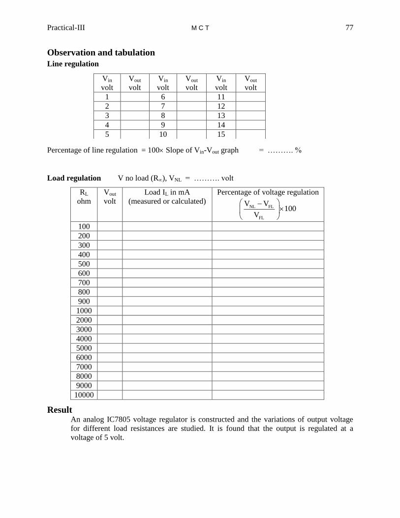
Observation and tabulation
Line regulation
Percentage of line regulation = 100 Slope of Vin-Vout graph = ………. %
Load regulation V no load (R), VNL = ………. volt
RL
ohm
Vout
volt
Load IL in mA
(measured or calculated)
Percentage of voltage regulation
NL FL
FL
V V100
V
100
200
300
400
500
600
700
800
900
1000
2000
3000
4000
5000
6000
7000
8000
9000
10000
Result An analog IC7805 voltage regulator is constructed and the variations of output voltage
for different load resistances are studied. It is found that the output is regulated at a
voltage of 5 volt.
Vin
volt
Vout
volt
Vin
volt
Vout
volt
Vin
volt
Vout
volt
1 6 11
2 7 12
3 8 13
4 9 14
5 10 15

78 Electronics Practical III
Exp.No.3.21
Op-amp- inverting and non-inverting amplifier, voltage follower
Aim: To construct and demonstrate the functioning of an inverting amplifier, non-inverting
amplifier and a voltage follower using operational amplifier 741 (OPAMP741).
Components and accessories: Operational amplifier (IC741), pillar tag board, resistor,
capacitor, signal generator, dual power supply C R O, etc.
Circuit, theory and procedure
Operational amplifier 741 is an integrated circuit that can be used as an inverting amplifier,
non-inverting amplifier and a voltage follower. It can also be used for other purposes as adder,
subtractor, differentiator, integrator etc. The symbol of it is shown in the fig.b.
Inverting amplifier: In the inverting amplifier the signal is applied to the inverting terminal 2 of
the opamp through the resistor Ri. The non-inverting terminal 3 is grounded. The negative
feedback takes place through the resistor Rf. The input and the output are measured by a C R O.
For all practical purposes, the inverting terminal (terminal 2) of the op-amp is very nearly zero
and thus it act as ‘virtual ground’. Due to the "virtual ground" effect the right-hand side of the
resistor Ri is held to a voltage of 0 volts. Since terminal 2 is at zero potential, practically no
NC
+V
Output
Offset Null
Offset Null
Inverting input
Non-inverting input
V
1
2
3
4
6
7
8
5
2 3
4 7
8
1
IC741
Operational amplifier
Pinout diagram of 741 Fig.a
3
2
4
6
7
+
symbol for inverting
+ symbol for non-inverting
Fig.b
3
2
7
4
6
15V
+15V
Sig
nal
gen
erat
or
C R O
Chanel 1
Rf =10K
IC741
Ri =10K
+
Fig.c
C R O
Chanel 2
i=iin=iout

Practical-III M C T 79
current flows through the opamp. Hence the same current must pass through Rf and the output
voltage vo must be opposite in sign of the input voltage vin. Current through Ri is given by,
iin = in
i
v
R = iout
Or, input voltage, vin = iinRi
Output voltage, vo = iinRf
Voltage gain, Av =o
in
v
v= f
i
R
R
The negative sign shows that the output is
inverted. Take observations for different
values of Ri and Rf.
Non-inverting amplifier: Because of the
virtual ground of terminal 2 and the short between the terminals 2 and 3 of the opamp, the input
voltage in this case is the p d across Ri and the output voltage is the p d across the series
combination of Ri and Rf.
Input voltage, vin = iRi
Output voltage vo = i fi R R
Voltage gain, Av =o
in
v
v= f
i
R1
R
The input and the output are measured by a C R O for different values of Ri and Rf.
Input
Output
with
gain 2
Fig.d: Input and output of inverting amplifier
3
2
7
4
6
15V
+15V
Sig
nal
gen
erat
or
C R O
Chanel 1
Rf =10K
IC741
Ri =10K
+
Fig.e
C R O
Chanel 2
i=iin=iout
Input
Output
with
gain 2
Fig.e: Input and output of non- inverting amplifier
3
2
7
4
6
15V
+15V
Sig
nal
gen
erat
or
C R O
Chanel 1
IC741
+
C R O
Chanel 2
Fig.f: Voltage follower
Input
Fig.g: Input and output of a voltage follower
Output

80 Electronics Practical III
Voltage follower: A voltage follower provides an output which is same as the input. The gain of
the voltage follower is very much closer to unity and there is no phase difference between input
and output.
Observation and tabulation
Inverting amplifier
Peak to peak voltage of input signal = 2 volt; Frequency of the signal = 500 Hz
Ri
K
Rf
K
No. of divisions
of peak to peak
of output
Volt per
division
Output
Voltage
VO volt
Observed
gain VO/Vi
Theoretical
gain Rf/Ri
10
10
20
30
40
50
60
70
80
90
100
1K
1
2
3
4
5
6
7
8
9
10
1
1K
2
3
4
5
6
7
8
9
10
Practical-III M C T 81
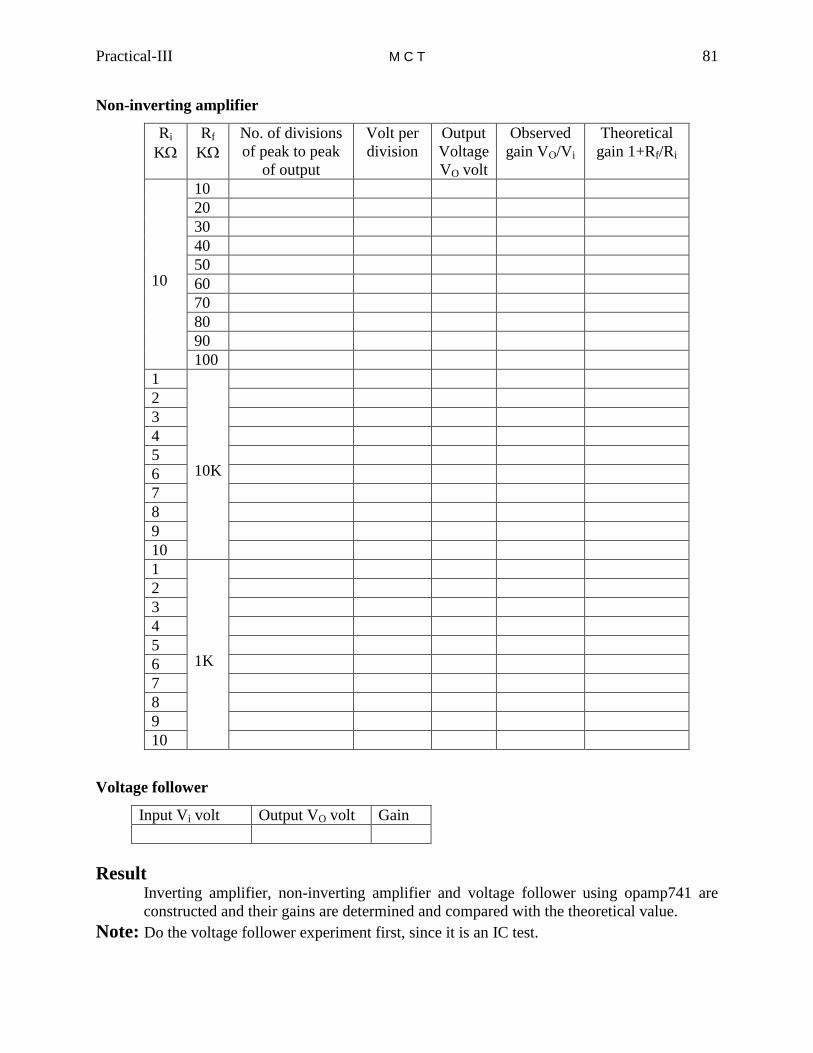
Non-inverting amplifier
Ri
K
Rf
K
No. of divisions
of peak to peak
of output
Volt per
division
Output
Voltage
VO volt
Observed
gain VO/Vi
Theoretical
gain 1+Rf/Ri
10
10
20
30
40
50
60
70
80
90
100
1
10K
2
3
4
5
6
7
8
9
10
1
1K
2
3
4
5
6
7
8
9
10
Voltage follower
Input Vi volt Output VO volt Gain
Result Inverting amplifier, non-inverting amplifier and voltage follower using opamp741 are
constructed and their gains are determined and compared with the theoretical value.
Note: Do the voltage follower experiment first, since it is an IC test.
82 Electronics Practical III
Exp.No.3.22
Op-amp –differentiator & integrator
Aim: To construct differentiator and integrator circuits using op-amp IC741 and study their
operation for different types of input wave.
Components and accessories: Operational amplifier (IC741), pillar tag board, resistor,
capacitor, signal generator, dual power supply C R O, etc.
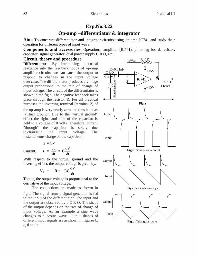
Circuit, theory and procedure Differentiator: By introducing electrical
reactance into the feedback loops of op-amp
amplifier circuits, we can cause the output to
respond to changes in the input voltage
over time. The differentiator produces a voltage
output proportional to the rate of change of
input voltage. The circuit of the differentiator is
shown in the fig.a. The negative feedback takes
place through the resistor R. For all practical
purposes the inverting terminal (terminal 2) of
the op-amp is very nearly zero and thus it act as
‘virtual ground’. Due to the "virtual ground"
effect the right-hand side of the capacitor is
held to a voltage of 0 volts. Therefore, current
"through" the capacitor is solely due
to change in the input voltage. The
instantaneous charge on the capacitor, q = CV
Current, i = dq
dt =
dVC
dt
With respect to the virtual ground and the
inverting effect, the output voltage is given by,
Vo = iR = dV
RCdt
That is, the output voltage is proportional to the
derivative of the input voltage.
The connections are made as shown in
fig.a. The signal from a signal generator is fed
to the input of the differentiator. The input and
the output are observed by a C R O. The shape
of the output depends on the rate of change of
input voltage. As an example a sine wave
changes to a cosine wave. Output shapes of
different input signals are as shown in figures b,
c, d and e.
3
2
7
4
6
15V
+15V
Sig
nal
gen
erat
or
C R O
Chanel 1
R=1K
IC741
C=0.01nF
+
Fig.a
C R O
Chanel2
iin=iout
Input
Output
Fig.b: Square wave input
Input
Output
Fig.c: Saw tooth wave input
Input
Output
Fig.d: Triangular wave
input

Practical-III M C T 83
Note
Different values of capacitors possible. Try with 0.01nF, 0.001nF, etc.
Different values of R also possible. Try with 1K, 2K, etc.
Wait for some time to get the wave form.
Put C R O in a c mode.
Input of the order of 6 volt signal from signal generator.
Output of the order of 100 mV.
Vary the input frequency from low value to KHz order.
Try for all type of signal forms, sine, square etc.
Integrator: An op-amp integrator circuit would generate an output voltage proportional to the
magnitude and duration that an input voltage signal has deviated from 0 volts. The integrator
circuit is shown in the fig.f. The negative feedback takes place through the capacitor.
Treating the inverting terminal 2 as virtual ground, the instantaneous current through the
resistance and capacitance is same. Thus, iin = io
i.e. inV
R =
dq
dt
q = invdt
R
Output voltage Vo = q
C
= in
1V dt
RC
Fig.e: Sine wave input
Output
Input
3
2
7
4
6
15V
+15V
Sig
nal
gen
erat
or
R=0.5K
IC741
C=1F
+
Fig.f
C R O
Chanel 1
C R O
Chanel 2
iin=iout
84 Electronics Practical III
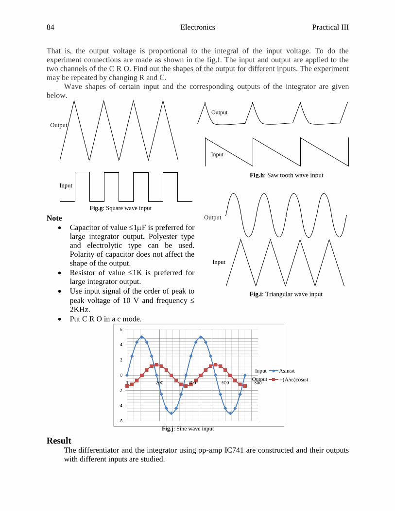
That is, the output voltage is proportional to the integral of the input voltage. To do the
experiment connections are made as shown in the fig.f. The input and output are applied to the
two channels of the C R O. Find out the shapes of the output for different inputs. The experiment
may be repeated by changing R and C.
Wave shapes of certain input and the corresponding outputs of the integrator are given
below.
Note
Capacitor of value 1F is preferred for
large integrator output. Polyester type
and electrolytic type can be used.
Polarity of capacitor does not affect the
shape of the output.
Resistor of value 1K is preferred for
large integrator output.
Use input signal of the order of peak to
peak voltage of 10 V and frequency
2KHz.
Put C R O in a c mode.
Result The differentiator and the integrator using op-amp IC741 are constructed and their outputs
with different inputs are studied.
Input
Fig.g: Square wave input
Output
Input
Fig.h: Saw tooth wave input
Output
Input
Output
Fig.i: Triangular wave input
Asint
(A/)cost
Input
Output
Fig.j: Sine wave input
Practical-III M C T 85
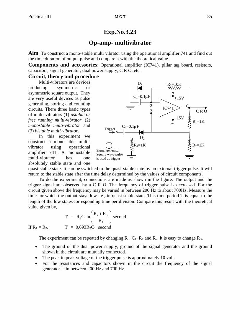
Exp.No.3.23
Op-amp- multivibrator
Aim: To construct a mono-stable multi vibrator using the operational amplifier 741 and find out
the time duration of output pulse and compare it with the theoretical value.
Components and accessories: Operational amplifier (IC741), pillar tag board, resistors,
capacitors, signal generator, dual power supply, C R O, etc.
Circuit, theory and procedure Multi-vibrators are devices
producing symmetric or
asymmetric square output. They
are very useful devices as pulse
generating, storing and counting
circuits. There three basic types
of multi-vibrators (1) astable or
free running multi-vibrator, (2)
monostable multi-vibrator and
(3) bistable multi-vibrator.
In this experiment we
construct a monostable multi-
vibrator using operational
amplifier 741. A monostable
multi-vibrator has one
absolutely stable state and one
quasi-stable state. It can be switched to the quasi-stable state by an external trigger pulse. It will
return to the stable state after the time delay determined by the values of circuit components.
To do the experiment, connections are made as shown in the figure. The output and the
trigger signal are observed by a C R O. The frequency of trigger pulse is decreased. For the
circuit given above the frequency may be varied in between 200 Hz to about 700Hz. Measure the
time for which the output stays low i.e., in quasi stable state. This time period T is equal to the
length of the low statecorresponding time per division. Compare this result with the theoretical
value given by,
T = 1 23 1
1
R RR C ln
R
second
If R1 = R2, T = 0.693R3C1 second
The experiment can be repeated by changing R3, C1, R1 and R2. It is easy to change R3.
The ground of the dual power supply, ground of the signal generator and the ground
shown in the circuit are mutually connected.
The peak to peak voltage of the trigger pulse is approximately 10 volt.
For the resistances and capacitors shown in the circuit the frequency of the signal
generator is in between 200 Hz and 700 Hz
3
2
7
4
6
15V
+15V
Signal generator
Square wave pulse
is used as trigger
Trigger
C R O
R2=1K
R1=1K
R3=10K
R4=1K
IC741
C2=0.1F
C1=0.1F
D2
D1
86 Electronics Practical III
See that the length of the lower side of the output does not change and the length of the
upper side changes when we change the frequency of the trigger pulse.
Put C R O either in a c or d c mode.
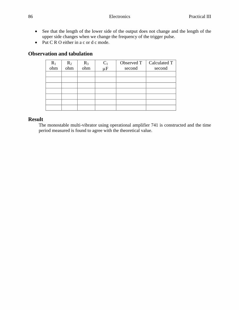
Observation and tabulation
R1
ohm
R2
ohm
R3
ohm
C1
F
Observed T
second
Calculated T
second
Result The monostable multi-vibrator using operational amplifier 741 is constructed and the time
period measured is found to agree with the theoretical value.

Practical-III M C T 87
Exp.No.3.24
Characteristics of JFET
Aim: To draw the common source drain characteristics and transfer characteristics of a junction
field effect transistor and hence to determine the JFET parameters a c drain resistance rd,
transconductance gm and the amplification factor .
Components and accessories: The JFET
(BFW10 or 11), power supplies, voltmeters, milli-
ammeter etc.
Circuit, theory and procedure Field effect transistor is a three terminal
unipolar solid state device in which the current is
controlled by the field. They are constructed as either
n-channel FET or P-channel FET. In n-channel FET
two p-type junctions are diffused on opposite sides of
a narrow bar of n-type semiconductor. A p-channel
FET is constructed by diffusing
n-type material on opposite sides
of a bar of p-type material.
There three terminals
connected to FET are source,
drain and gate. Source is the
terminal through which the
majority carriers enter the bar.
Drain is the terminal through
which the majority carriers leave
the bar. Gate is two internally
connected heavily doped regions
which form two P-N junctions.
Gates are always reverse biased.
They control the current through
the FET. (There is a fourth
terminal on a BFW10 or 11
FET. This terminal is connected
to the body of the FET.
D
G
Body
S
Fig.b: FET with pins upward
V
mA
V
+
+
+
Fig.c
10V 3V S
D
G
Fig.d
VGS = 0 V
VGS = 0.5V
VGS = 1V
VGS = 1.5V
VGS = 2V
B
A
C
N N N P P P
S S
D D
G G
p-channel n-channel
Fig.a

88 Electronics Practical III
We now draw two
characteristics of a JFET. They
are static characteristics or
common source characteristics or
drain characteristics and transfer
characteristics. The common
source characteristics is the graph
between drain current ID and
drain-source voltage VDS for
constant gate-source voltage VGS.
We can draw a family of curves
for different gate-source voltages
as shown in fig.d.
The region OA of the graph
is called the ohmic region in
which the current is proportional
to the voltage VDS. In the curve region AB the current changes at inverse square law rate. The
point B is called the pinch-off point. The voltage corresponding to it is called the pinch-off
voltage and is denoted as VPO. The region BC is called the pinch-off region (C is the point at
which the current again increases sharply nearly 20 V, which is not shown in the graph) or
saturation region or amplifier region.
Transfer characteristics is the graph between the drain current ID and the gate-source
voltage VGS as shown in fig.e. The transfer characteristic is obtained from the drain
characteristics. For a constant VDS we get different values of ID corresponding to different values
of VGS.
To do the experiment, connections are made as shown in the fig.c. Keep VGS constant, say
zero and measure the drain current ID for different VDS. A graph is drawn between ID and VDS.
Repeat the experiment for different negative voltages for gate and the family of curves is drawn
on the same graph paper.
From the drain characteristics (or from the same observations for drain characteristics) we
get ID for different VGS. Draw the graph between ID and VGS.
To find the FET parameters rd, gm and : The FET parameters are a c drain resistance rd,
Transconductance gm, and the Amplification factor . They are defined as follows.
When JFET is operating in the pinch off region,
a c drain resistance rd = DS
DGS
V
V
I
It is the slope of the drain characteristics in the pinch-off region.
Transconductance gm, = D
GSDS
V
I
V
It is the slope of the transfer characteristic. Its unit is siemen.
ID
Fig.e

Practical-III M C T 89
Amplification factor = DS
GSD
I
V
V
It can be proved that, = d mr g
Pins near the projection are either source or body. Using multi-meter check the continuity
of pin connected to the body and identifies it. Then the other one is source. In the
clockwise direction drain and gate.
Practically we can find out the FET parameters near the pinch-off region (curved region
AB).
Observation and tabulation
To draw drain characteristics
VDS
volt
Drain current ID in mA for VGS =
0 V 0.5 V 1 V 1.5 V 2 V
0
0.5
1
1.5
2
2.5
3
3.5
4
4.5
5
5.5
6
6.5
7
7.5
8
To draw transfer characteristic
Constant VDS
volt
Drain current ID in mA for VGS =
0 V 0.5 V 1 V 1.5 V 2 V
Result The characteristics of FET are drawn and the FET parameters are determined.
Drain resistance rd = ……… ohm
Transconductance, gm = ……… mho
Amplification factor, = ………