thomas n. theis director, physical sciences ibm research
TRANSCRIPT

T.N. Theis 3/25/03 Research
Thomas N. TheisDirector, Physical SciencesIBM Research Almaden - Yorktown - Zurich
Nanotechnology:A Look into the Future

T.N. Theis 3/25/03 Research
Topics ...
Why is IBM pursuing research in nanoscale scienceand technology?
Self-assembly - the challenge to do it better
Outlook

T.N. Theis 3/25/03 Research
Nanotechnology is...
“Research and technology development at the atomic, molecular or macromolecular levels, in the length scale of approximately 1 – 100 nm range…”
National Science Foundationwww.nsf.gov/home/crssprgm/nano/omb_nifty50.htm
T.N. Theis 3/25/03 Research
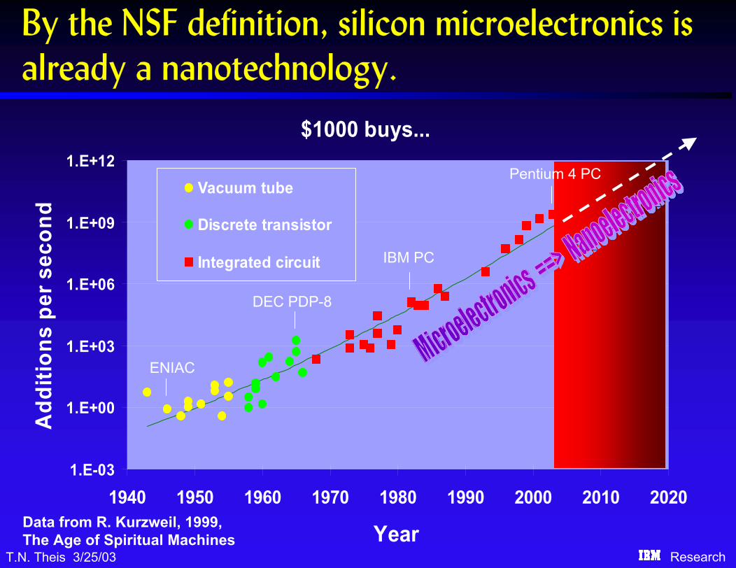
By the NSF definition, silicon microelectronics is already a nanotechnology.
$1000 buys...
1.E-03
1.E+00
1.E+03
1.E+06
1.E+09
1.E+12
1940 1950 1960 1970 1980 1990 2000 2010 2020
Year
Add
ition
s pe
r sec
ond
Vacuum tube
Discrete transistor
Integrated circuit
Data from R. Kurzweil, 1999, The Age of Spiritual Machines
ENIAC
DEC PDP-8
IBM PC
Pentium 4 PC

T.N. Theis 3/25/03 Research
The silicon transistor has become a nanodevice.
Bulk SOI
130 nm
Double-gateGround plane
Ultimate double gate
10 – 15 nm ?

T.N. Theis 3/25/03 Research
An Experimental Silicon Transistor
TSi=7nm Lgate=6nm
Source Drain
Gate
B. Doris et al., IEDM , 2002.

T.N. Theis 3/25/03 Research
Approaching the ultimate silicon nanodevice(a double-gate Transistor or FinFET)
Poly-SiTsi=20nm Tox=1.6nm H=65nm
BOX
TEOS
H
Tsi
TEM
SEM
Tox = 1.6nm
Poly-Si
Si
TEM
60 nm channel length FET
Cross-section

T.N. Theis 3/25/03 Research
Is there a successor to silicon?
Organic Electronics?Molectronics? Spintronics?
Quantum Computing?
DNA Computing?:
i100 nm
NanoscaleScience and Technology
principle features specified to: i1mm
i10 m

T.N. Theis 3/25/03 Research
Attributes of Successful Digital Logic Devices
• Output drives the input• Signal level restoration• Noise immunity• Global as well as localcommunications
After H.-S. P. Wong, “Novel Device Options” in Sub-100nm CMOS Short Course, IEDM, 1999

T.N. Theis 3/25/03 Research
“Revolutionizing” a large, complex, stratified industry is not easy.
• Sphere of successful influence: +/- one layer
ApplicationArchitecture
SystemCircuitDevice
MaterialsPhysics/chemistry
Adapted from M. Horowitz, in Focus Center Research Program (MARCO) MSD-C2S2 Topical Workshop, Nov. 12, 2001
T.N. Theis 3/25/03 Research
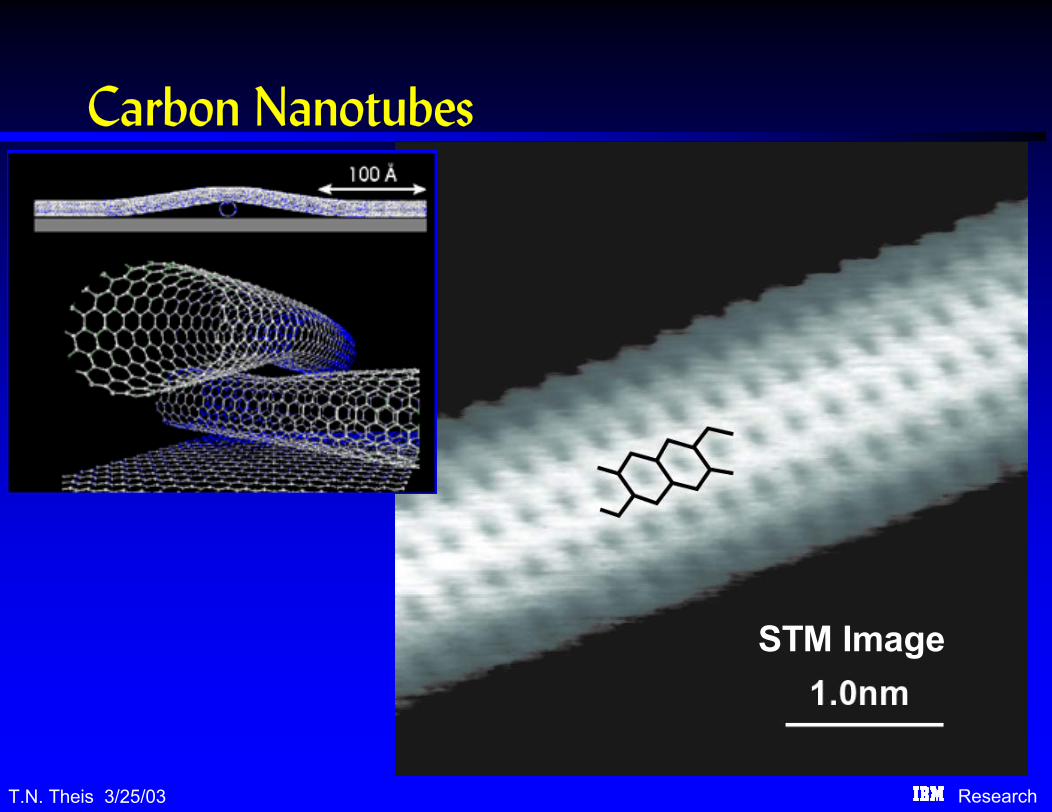
Carbon Nanotubes
STM Image

T.N. Theis 3/25/03 Research
An alternative logic switch --A simple Carbon Nanotube Transistor

T.N. Theis 3/25/03 Research
Carbon nanotube intra-molecular logic gate (NOT gate, voltage inverter)
-2
-1
0
1
2
-4 -2 0 2 4VIN (V)
V OU
T (V)
Gain>1
T.N. Theis 3/25/03 Research
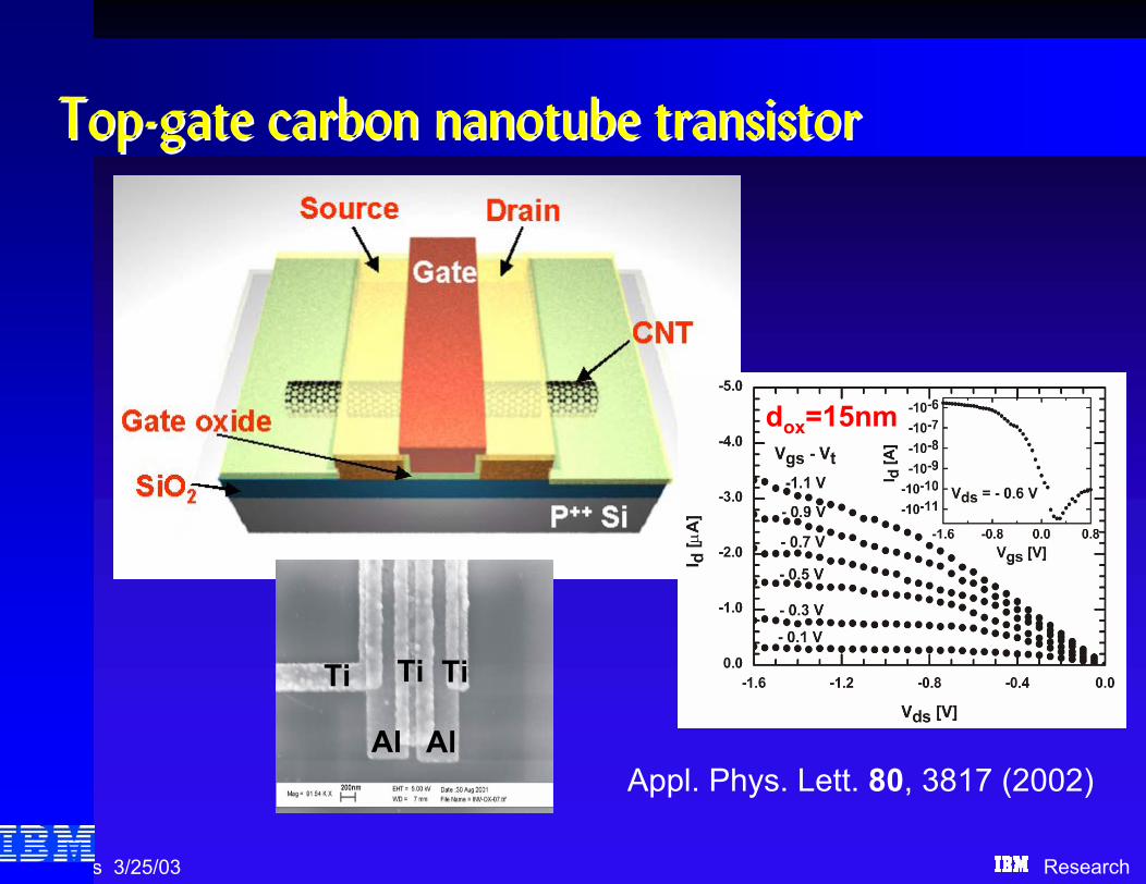
Ti Ti Ti
Al Al
dox=15nm
TopTop--gate carbon nanotube transistorgate carbon nanotube transistor
Appl. Phys. Lett. 80, 3817 (2002)

T.N. Theis 3/25/03 Research
Comparison with siliconComparison with silicon
threshold voltagethreshold voltage --0.2V0.2V --0.5V0.5V
drive currentdrive current 2100mA/mm2100mA/mm650mA/mm650mA/mm(Vg(Vg--Vt=Vt=--1.0V)1.0V)
gate oxide thicknessgate oxide thickness 1.5nm1.5nm ~15nm~15nm
transconductancetransconductance 2300mS/mm2300mS/mm650mS/mm650mS/mm
channel lengthchannel length 50nm50nm 260nm260nm
pp--MOSFET MOSFET a)a) pp--CNFETCNFET
IIOnOn/I/IOffOff ~10~1066101066 -- 101077
subthreshold slopesubthreshold slope 70mV/dec70mV/dec 130mV/dec130mV/deca) R. Chau et al. Proceedings of IEDM 2001, p.621

T.N. Theis 3/25/03 Research
Carbon nanotube transistors have promise
Carrier transport is ballistic and ambipolarAll bonds are satisfied, stable, and covalentChemical synthesis controls a key dimensionDevice is not “wed” to a particular substrate
because:
but much remains to be done:ScalabilityContactsDopingDevice stability (charge trapping)High yield, selective growth of nanotubes(control of the diameter, length, chirality, position)

T.N. Theis 3/25/03 Research
Memory Everyone wants non-volatile, low-power memory.Everyone wants a dense cross-point memory.
IB
W
I
WL
WL
SLSL
Amplifier
Current for write
Sensepath
Select column
Select row
There is no conceptual problem with bistable hysteretic two-terminal devices as cross-point memory cells.

T.N. Theis 3/25/03 Research
Memory Landscape
volatile non-volatile1Transistor 1T-DRAM Floating-gate
SONOSSET
Multiple Transistor SRAM1T-1C DRAM FeRAM1T-1R MRAM
polymer RAMmolecular memoryphase-change RAMperovskite MIM RAM
1R (Cross-point) MRAMpolymer RAMmolecular memoryperovskite MIM RAM

T.N. Theis 3/25/03 Research
Memory (continued) • There is no shortage of two-terminal, bistable
hysteretic memory devices and materials!
– MTJ MRAM (IBM/Infineon, Motorola, Toshiba, NEC, Sony, HP, Honeywell, Micromem, Motorola, NVE, Samsung, USTC, Toshiba)
– Chalcogenide glasses (Intel/Ovonyx, Micron Technology/Axon Technologies, Samsung, ST Micro)
– Polymeric resistive memory (Intel/Opticom, AMD/Coatue)– Molecular memories (Hewlett Packard, Molecular
Electronics Corp., Zettacore, Nantero, …)
• But ...– All memories require logic devices for read/write.
Candidate memory cells must be integrated with logic. – Replacing a transistor-based memory cell with a cross-
point cell will typically reduce performance.

T.N. Theis 3/25/03 Research
Millipede: A nanomechanical approach to storing information

T.N. Theis 3/25/03 Research
The Quantum Mirage: Single Channel Information Transport
Topograph
dI/dV difference

T.N. Theis 3/25/03 Research
Multi Channel Information Transport
Topograph
dI/dV difference

T.N. Theis 3/25/03 Research
But how can we position atoms cheaply?
Persuade them to assemble themselves!

T.N. Theis 3/25/03 Research
Nature's Self-Assembly
http://www.its.caltech.edu/~atomic/snowcrystals/photos/WWick/wwick.htm
T.N. Theis 3/25/03 Research
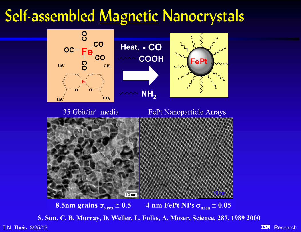
Self-assembled Magnetic Nanocrystals
S. Sun, C. B. Murray, D. Weller, L. Folks, A. Moser, Science, 287, 1989 2000
15 nm
8.5nm grains σarea ≅ 0.5 4 nm FePt NPs σarea ≅ 0.05
35 Gbit/in2 media FePt Nanoparticle Arrays
O
O
CH3
O
O
H3C
Pt
FeCO
CO
CO
CO
OC
CH3H3CFePt
- COHeat,COOH
NH2

T.N. Theis 3/25/03 ResearchF. X. Redl, K. S. Cho and C. B. Murray.
AB13 binary Nanocrystal Superlattice of PbSe and Fe2O3
Multi-Component Nanocrystal Superlattices

T.N. Theis 3/25/03 Research
T. J. Watson Research Center
40 nm40 nm
(100) View (110) View
20 nm500 nm
Straight PbSe Nanowires
Semiconductor Nanowires
Branched PbSe Nanowires with High Surface Area

T.N. Theis 3/25/03 Research
200 nm
Self-assembly: SiGe Quantum Dots
T.N. Theis 3/25/03 Research
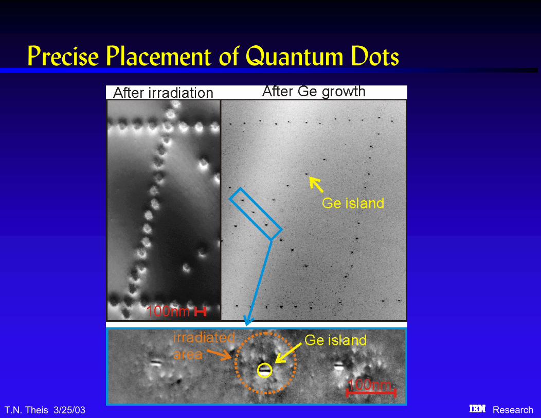
Precise Placement of Quantum Dots

T.N. Theis 3/25/03 Research
Self Assembly: A One-Monlayer-Thick Pentacene “Snowflake”
50 m

T.N. Theis 3/25/03 Research
Thin Film Transistors on Transparent Plastic:
µ = 0.2 to 0.4 cm2 V-1s-1, operating voltage 0 to 4 V.All fabrication processes done at room temperature.

T.N. Theis 3/25/03 Research
Patterning Silicon with Block Co-polymers

T.N. Theis 3/25/03 Research
Pourous Dielectrics for On-Chip Wiring
T.N. Theis 3/25/03 Research
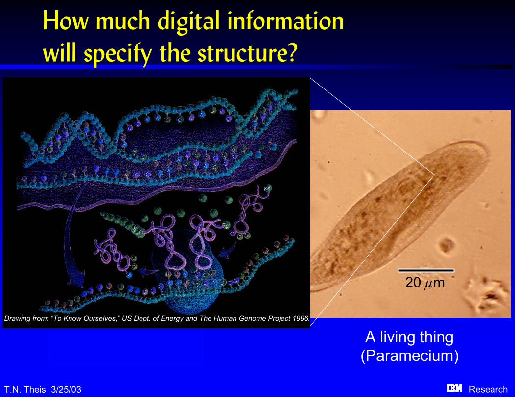
How much digital information will specify the structure?
IBM eServer p690
20 m
200 nm
20 m
A living thing (Paramecium)
Drawing from: “To Know Ourselves,” US Dept. of Energy and The Human Genome Project 1996.

T.N. Theis 3/25/03 Research
How much digital information is needed to BUILD the structure?
• Microprocessor – Gigabytes
• Living Thing – Megabytes!

T.N. Theis 3/25/03 Research
Nanotechnology ...
The ability to design and control the structure of an object on all length scales, from the atomic to the macroscopic.

T.N. Theis 3/25/03 Research
Nanotechnology: We’re just getting started.
$1000 buys...
1.E-03
1.E+00
1.E+03
1.E+06
1.E+09
1.E+12
1940 1950 1960 1970 1980 1990 2000 2010 2020
Year
Add
ition
s pe
r sec
ond
Vacuum tube
Discrete transistor
Integrated circuit