thesis - optimization of plasma enhanced chemical vapor deposition of ultra thin high resistivity...
TRANSCRIPT

1
Bachelor thesis
Of Mina Jean Hanna
In the subject of characterization and modeling of group III nitrides Heterostructure Field Effect
Transistor
Titled: optimization of plasma enhanced chemical vapor deposition of ultra thin high resistivity
silicon nitride films for gate insulation for GaN MISHFETs
Written and research done in
Institut für Theoretische Elektrotechnik
Lehr- und Forschungsgebiet GaN-Bauelementtechnologie Univ.-Prof. Dr.-Ing. Andrei Vescan
Der Fakultät für Elektrotechnik der Rheinisch-Westfälischen Technischen Hochschule Aachen
University of Texas, Austin, TX, USA
January 2010

2
Table of Contents:
1. Introduction ……………………………………………………………………………………………………………………………….. [5]
1.1 Overview and aim.………………………………………………………………………………………………………… [5]
1.2 Motivation ……………………………………………………………………………………………………………………. [7]
1.2.1 Group III Nitrides properties………………………………………………………………………….. [8]
1.3 Dielectric optimization & statistical analysis approach………………………………………………….. [12]
1.4 Extracting the trends from JMP simulations………………………………………………………………….. [15]
2. CVD of Nitrides…………………………………………………………………………..……………………………………………….. [17]
3. Theoretical Background………………………………………………………………………………………………………………. [21]
3.1Plasma……………………………………………………………………………………………………………………………. [21]
3.2 Collision Cross Section…………………………………………………………………………………………………… [25]
3.3 Deposition techniques…………………………………………………………………………………………………… [33]
4. Experimental work……………………………………………………………………………………………………………………….. [37]
4.1 Processing of samples…………………………………………………………………………………………………….. [37]
4.2 Samples testing………………………………………………………………………………………………………………. [41]
4.3 Responses and Results……………………………………………………………………………………………………. [46]
4.3.1 Deposition rate……………………………………………………………………………………………….. [46]
4.3.2 Refractive index………………………………………………………………………………………………. [47]
4.4 CV measurements………………………………………………………………………………………………………….. [49]
4.4.1 MIM/MIS capacitor behavior………….………………………………………………………………. [49]
4.4.2 Dielectric constant at 1MHz…………………………………………………………………………….. [53]
4.5 IV measurements ……………………………………………………………………………………………………………. [54]
4.5.1 Low electric field current polarity..………………………………………………………………….
4.5.2 Fittings to PF emission and FN tunneling…………………………………………………………
4.6 Characterization of traps, detrapping/ depolarization currents……………………………………… [59]

3
4.6.1 CV dependency in MIM structures…………………………………………………………………. [59]
4.6.2 Stressed conduction currents …………………………………………………………………………. [62]
4.6.3 Depolarization of trapped space charge on SiN/TiN structures………………………. [64]
5. Recent MISHFET results & current work……………………………………………………………………………………….. [67]
6. Conclusion & Outlook……………………………………………………………………………………………………………………
7. References………………………………………………………………………………………………………………………………. [69]
8. Appendix [A]: Silicon nitride characteristics…………………………………………………………………………………… [75]

4
First of all, I would like to present my deepest thanks and gratitude to those who first gave me the
opportunity to join this research facility in RWTH Aachen, and take advantage of these state of art
equipments and advanced tools that I can handle and operate directly and freely whenever I have an
idea of an experiment or a refinement of my results.
Second, for all the help and support they offered me during the time of the thesis and even the period
prior to the thesis with all the coordination and handling of official –bureaucratic- measures needed. And
for the fruitful discussions and assistance provided from every member of the institute and their care to
clear my doubts and answer all my inquiries.
I specify here within my deepest gratitude for:
Prof.Dr-Ing Andrei Vescan, head of the institute and my advisor.
Dipl Ing. Martin Eickelkamp, my direct supervisor and mentor.
And of Course: Prof. Dr-Ing Darek Korzec, former Dean of the faculty of Information Engineering and
Technology who gave me the first insight into this field.
And for all the members of the ITHE
Dr.rer.nat Holger Kalisch,
Dipl Ing. Nico Ketteniß,
M.Sc Lars Rahimzadeh Khoshroo,
Dipl Phys Frank Jessen,
Dipl Ing Christian Lautensack
Dipl cand- Ing. Bjorn Alan Dresen
Dipl Ing. Christoph Mauder.
Dipl cand-Phys Hassan Boukiour

5
1. Introduction
1.1 Overview and aim of the project
The following thesis is based upon the research done during the period of 4 months from April 2009
through July 2009 in the institute of theoretical electrical engineering of RWTH Aachen. The main
purpose of this work is to analyze the behavior of chemical vapor deposition of Silicon Nitrides and their
material characteristics; to show the degree of correlation between the deposition process parameters
and the film properties and the way the parameters influence these properties for optimizing the gate
dielectric of AlGaN/GaN Metal Insulator Semiconductor HFETs.
AlGaN / GaN heterostructure transistors are very promising in high voltage, high power and hostile high
temperature environments. The main feature of this structure is the spontaneous and piezoelectric
polarization at the interface of the AlGaN/ GaN which induces a two dimensional electron gas having the
same functionality of a MOSFET channel but without doping [22] [24]. Different gate dielectrics have
been studied and experimentally used for effective insulation of gate contacts instead of using Schottky
gates that arise the problem of non negligible leakage currents caused by deteriorated metal / AlGaN
interface and low barrier height. Gate dielectrics which are usually amorphous are placed as an
intervening layer between the metal and the AlGaN crystal thus eliminating more or less to a certain
extent the bad interface leakage and reducing input capacitance.
Different dielectric materials have been used with different dielectric constants like SiO2 [24] [25];
Al2O3 [21] [26] and also SiN [23] [25] [27] . Even oxides like hafnium dioxides that are known to be a
high-k dielectric material [28]. All of these oxides have different setbacks that limit the MISHFET
operationability when incorporated under the gate. Taking for example Silicon Dioxide is a very good
insulator but limits the performance of AlGaN/GaN MISHFETs in high frequency. Another example
hafnium dioxide suffers from huge components of electron trapping generated by positive oxygen
vacancies [29]; thus in being used, it faces serious possibilities of performance degradation and PBTI
“positive bias temperature instability” and NBTI “negative bias temperature stability” jeopardizing
device reliability; PBTI generally comprises generation of donor like interface states while NBTI
comprises generation of interface state and bulk charge; these –when incorporated as gate insulators-
shift the threshold voltage of the device when under continuous stress.
Silicon nitride films in contrast show interesting traits and features for this application and many others.
SiN has been used for many decades since the start of the semiconductor industry revolution in
passivating active devices on ICs’ surfaces. Its known high resistivity, non vulnerability to react
chemically with active oxygen reagents and its resistance for oxygen diffusion during oxidation
processes in the various steps of the manufacturing flow nominates silicon nitride films to be a great
candidate as passivation layers. Additionally it forms a very good barrier to water and sodium and

6
potassium ions diffusion. Plus it is also used in packaging technology taking into consideration these
properties.
More of its properties have been used and thoroughly investigated for many different applications, like
metal-insulator-metal capacitors in VLSI technology [20] [34], surface wave devices [14] and solar cells
[17] for its low surface recombination rates, high bulk passivation and good anti-reflection properties. As
far as our application, the electronic properties of silicon nitride are the ones of interest including
relatively high dielectric constant, resistivity i.e. leakage currents suppression and high break down
electric field which is a very relevant parameter since the intended thickness of the insulator shouldn’t
be more than 10nm. Since the anticipated thickness is so shallow, the deposition processes that should
be tested should have a reasonable length of deposition time thus allowing a stable operation of the
PECVD tool and enough time for the Plasma to stabilize. Then eventually these processes would be
reproducible.
For that the deposition process should be optimized to achieve the expected thickness and the desired
electronic properties. For the optimization process an additional set of information is required about the
physics and the mechanics of the tool for successfully processing high performance AlGaN/GaN
MISHFETs. Although this work is not intended to be theoretical and it will be experimental, the data and
results that will be deduced will be compared and contrasted with theory. A systematic approach for
investigating these mechanics is deployed in this work through a statistical method called ‘Design Of
Experiment’; i.e. measurements taken are evaluated through a statistical software to construct a linear
regression model and estimating how much each parameter is influencing the output tested. Moreover,
mutual interaction –if existing- will be discovered by the model.
These parameters will encompass the important control inputs of the PECVD of Silicon nitride: chamber
pressure, table temperature, Radio Frequency source power, flow of input gases, and their ratio.
Deposition time was not considered as an influencing restriction or as a discrete factor by itself affecting
the output characteristics based on the assumption that the operation of PECVD is a linear time
invariant function; in other words that by increasing the time interval, a thicker deposited layer is
obtained not an altering in electrical resistivity or refractive index which represent indirectly a change in
the film composition or stoichiometry for instance. However, this assumption is not definitely absolute,
probably it can only be valid if the interval of time is –roughly- relatively longer than a minute; and that
is the first task that was achieved.
A theoretical background on plasma physics and PECVD process is necessary to be compiled in this
manuscript to explain, interpret or at least correlate the actual results gotten from the real experiment
with the long known and long developed theories.

7
1.2 Motivation
What is needed to be accomplished in this work is to understand more the variations of the inputs and
their consequences on the output parameters but most importantly in the contour of the intended
application. As a matter of fact SiN PECVD optimization has been emphasized before and many papers
have been produced about this topic. However, they were looking for certain parameters of importance
to other applications like refractive index [18] [19] [38], effective lifetime [17] [38], surface
recombination and charge density [38]…etc. These studies were for solar cells applications and / or
optimized using neural networks method. Others were investigating silicon nitride’s electrical properties
and / or PECVD optimization to be used as a dielectric layer for VLSI capacitors [20] [32] [34]; but they
were investigating each parameter alone without considering the possibility of parameter interactions in
the examined qualities. For this purpose, an exhaustive set of permutation of these parameters had to
be carried out and a linear regression had to be computed. Also, regarding the application of MISHFETs,
other papers were examining the device properties but with the insulator layer deposited by other
methods like ECR sputtering [23] or grown in situ over the AlGaN layer in the MOCVD reactor [51].
In the context, it is anticipated that by using different test methodologies in analyzing the electrical
properties of the dielectric through depositing a complete set of samples, a linear model will be
constructed conveying each parameter influence on the output and their cross interaction. It is
anticipated that the deposition rate, refractive index, dielectric constant, capacitance-voltage
dependency, bulk traps and Poole Frenkel / Fowler Nordheim tunneling conduction currents will be
characterized and correlated to RF power, deposition pressure, table temperature and ratio. It is also
anticipated that based on these informations, successful MISHFET devices exhibiting superior
characteristics: low leakage currents, less interface states, higher break down voltages, higher sheet
carrier concentration and high frequency operability, etc… will be processed.

8
1.2.1 Group III Nitrides properties1
Figure 1
Gallium nitride in general possess many attracting features -scoring much better than silicon if
compared- that are of extreme use for novel devices applications; it has wurtzite crystal structure and is
known with a direct wide bandgap (table[1]). Additionally Gallium nitride possesses higher saturation
velocity –around twice the value- of the silicon which is always limiting the range of frequencies that
silicon transistors can operate at. It was also found that GaN transistors can operate at higher
temperatures and higher voltages than the GaAs transistors making them idyllic efficient contenders for
power amplifiers at microwave frequencies.
GaN is distinguished by very high hardness, mechanical stability a large heat capacity necessary for high
temperature applications [44]. It has a remarkable resistance to cracking if in a pure form and can be
deposited in thin film on sapphire –this is the substrate we use for our AlGaN/GaN devices- or silicon
carbide. GaN can be doped with silicon (Si) or with oxygen to form N-type and with magnesium (Mg) to
form P-type, however the Si and Mg atoms change the way the GaN crystals grow, introducing tensile
stresses additional brittleness and fragility to the crystal [45]. With this feature, GaN PN junctions are
plausible applications; but unfortunately gallium nitride compounds also tend to have a high frequency
of spatial defect occurrences, on the order of a hundred million to ten billion defects per square
centimeter.
GaN AlN Si GaAs Band gap Energy (eV) 3.42 6.2 1.1 1.42
Saturation velocity (107cm/s) 2.7 2.0 1.0 2.0
Break down field strength (MV/cm) 3.3 11.7 0.3 0.4
Thermal Conductivity (W/cm.K) 4.1 5.9 1.3 0.45 Table 1 [41]
GaN crystals with high quality can be manufactured by Molecular Beam Epitaxy or Metalorganic Vapor Phase Epitaxy and is also possible by low temperature deposited buffer layer technology [46]. Different applications have been emphasized and experimented including: GaN p-n junction blue/UV-LEDs and
1 For detailed theoretical analysis and device characterization, refer to [9-11], [41], [43]
Yellow atoms Gallium Ga
Grey atoms nitrogen N [0001]
1
a
c
9
room-temperature stimulated emission for laser operation. Following this trend, high-performance blue LEDs and long-lifetime violet-laser diodes (LDs) were widely commercialized; beside nitride-based devices such as UV detectors and high-speed Field Effect Transistors that are the application for this thesis.
Nearly all of the primary colors of the visible spectrum were achieved by high-brightness GaN light-emitting diodes (LEDs), applications such as daylight visible full-color LED displays, white LEDs and blue laser devices became possible. The first GaN-based high-brightness LEDs were using a thin film of GaN deposited via MOCVD on sapphire. Other substrates used are zinc oxide and silicon carbide.
High-power/high-frequency devices based on GaN include microwave radio frequency power amplifiers (such as used in high-speed wireless data transmission) and high-voltage switching devices for power grids. This is in addition to GaN-based RF transistors that could be employed as microwave sources for microwave ovens, replacing the magnetrons currently used. Better performance than silicon in high temperature applications is maintained with the large band gap of GaN. First Gallium Nitride metal/oxide semiconductor field-effect transistors (GaN MOSFET) were experimentally fabricated and characterized in 1993 [47] and currently tremendous amount of research is being deployed in this field.
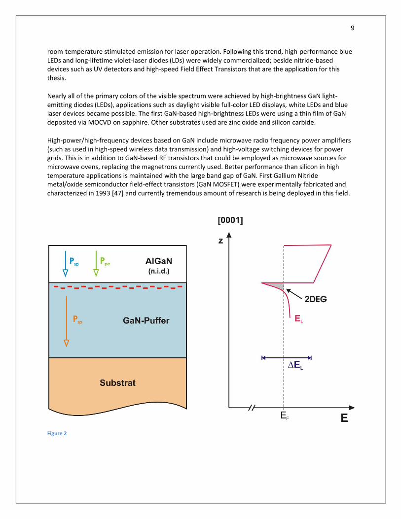
Figure 2

10
The second point of interest in Gallium Nitride is manifested when a contact with Aluminum Gallium
Nitride is created. At their interface forms a 2 dimensional electron gas (2DEG); in other words a high
density of electrons free to move in 2 dimensions and confined in the third forming a sheet region
where it could reach around 1013 cm-2 before applying any doping to the material. The most common
application where a 2DEG-like channel is found is the MOSFET in the strong inversion mode where
carriers are confined underneath the gate oxide at the semiconductor-oxide interface. But unlike the
MOSFET, the AlGaN/GaN heterojunction’s 2DEG enjoys the privilege of much higher mobility since
intentionally this 2DEG channel is undoped thereby mitigating the deleterious effect of ionized impurity
scattering or damaging to the crystal structure induced by ion implantation.
Furthermore, this 2DEG exits even before any external fields are applied unlike the MOSFET case. Due to
the electronic structure of the nitrogen and gallium atom in the wurtzite crystal unit structure and as a
consequence of its lower symmetry compared to the cubic zincblende structure, a spontaneous
polarization Psp comes into effect; permanent microscopic dipoles oriented are created in the C direction
of the crystal structure. In addition to that, also due to the noncentrosymmetry of the wurtzite crystal a
piezoelectric polarization is induced. The piezoelectric polarization field is related to the stress jand
strain jtensors by the piezoelectric moduli dijk and eijk types as in equation (1).
(1)
Spatial variations in the spontaneous and piezoelectric polarization fields gives rise to a polarization-
induced electrostatic charge gradient, pol accompanied by an electrostatic potential (2) and non aligned Fermi level at the interface.
(2)
To align Fermi level, induced charges occupy the surface states at the mutual interface (fig. [2]) and the
2DEG region with very high mobility carriers is created.
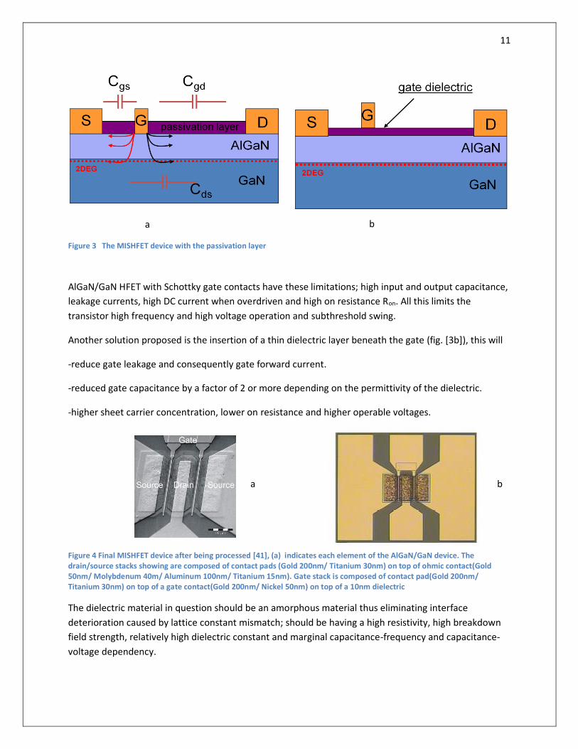
However, the device encounters a major problem with the gate designed as a Schottky contact; due to
deteriorated interface and low barrier height of the metal/AlGaN contact, non negligible currents tunnel
through the gate to the AlGaN bulk and reaching the 2DEG region. Consequently the device
performance is greatly challenged to the anticipated theoretical limits. One solution that has been
proposed is to introduce a dielectric layer as a passivation layer (fig [3a]) to saturate the interface states
at the surface around the gate contact. Interestingly enough this dielectric layer introduces another
stress factor to the tensile strained AlGaN crystal and ideally it increases the sheet carrier concentration
in the 2DEG region [9]. But still leakage currents have not been suppressed.
11
Figure 3 The MISHFET device with the passivation layer
AlGaN/GaN HFET with Schottky gate contacts have these limitations; high input and output capacitance,
leakage currents, high DC current when overdriven and high on resistance Ron. All this limits the
transistor high frequency and high voltage operation and subthreshold swing.
Another solution proposed is the insertion of a thin dielectric layer beneath the gate (fig. [3b]), this will
-reduce gate leakage and consequently gate forward current.
-reduced gate capacitance by a factor of 2 or more depending on the permittivity of the dielectric.
-higher sheet carrier concentration, lower on resistance and higher operable voltages.
Figure 4 Final MISHFET device after being processed [41], (a) indicates each element of the AlGaN/GaN device. The drain/source stacks showing are composed of contact pads (Gold 200nm/ Titanium 30nm) on top of ohmic contact(Gold 50nm/ Molybdenum 40m/ Aluminum 100nm/ Titanium 15nm). Gate stack is composed of contact pad(Gold 200nm/ Titanium 30nm) on top of a gate contact(Gold 200nm/ Nickel 50nm) on top of a 10nm dielectric
The dielectric material in question should be an amorphous material thus eliminating interface
deterioration caused by lattice constant mismatch; should be having a high resistivity, high breakdown
field strength, relatively high dielectric constant and marginal capacitance-frequency and capacitance-
voltage dependency.
a
n
b
a
a
a
a
b
a b
12
1.3 Dielectric optimization and statistical analysis approach
Silicon Nitride deposited by Plasma Enhanced Chemical Vapor Deposition is the dielectric material that is
investigated in this work. PECVD process is a deposition technique where two or more gaseous
precursors react chemically producing a solid compound that adsorbs, to the surface of the specimen
during the surface reaction; while other byproducts desorbs to the chamber ambient and is pumped
out trough the exhaust valve of the PECVD. Additionally, reactants are in their plasma state by being
excited by a microwave source to enhance the chemical reaction of the precursors. The key feature of
the PECVD lies in its processing that allows deposition at much lower temperatures which is often
critical in the manufacturing of semiconductors. Equations [3-5] are the reactions used to deposit silicon
from the gas phase, the one that will be used in our OXFORD PECVD reactor is (equ. [3]);
(3)
(4)
(5)
The statistical methodology used in this work is design of experiment -DoE- by which a linear regression
model will be constructed for multiple measured responses correlating them to the process inputs. The
model is a linear function combining single inputs, 2 inputs joints and computed respective correlation
coefficients revealing the degree of influence of each parameter and / or inputs’ mutual interaction on
the response. Leverage plots will be plotted to show the way this influence manifests itself. (sec. [1.4])
Design of experiment is by definition: “The design of all information gathering exercises where variation
is present. It is done because of the interest in the effect of some process or intervention on some object
which is called the experimental unit”.
Figure 5

13
The DoE 2 in principle is a permutation of x input parameters - those are the characteristics of the PECVD
process; 4 of them will be accounted for- with two degrees of freedom or two values for each either Y or
Z; that is counting to 24. In a way to examine the output of the process by changing -with taking all
possible combinations- one input at a time and then two inputs together, then three, then all four
together… The DoE is a statistical approach to associate the input and the output to find a relation in
how the input will change the output; or even better, it is a systematic approach in correlating the
theory and its predictable outcomes with the practical consequences of a process.
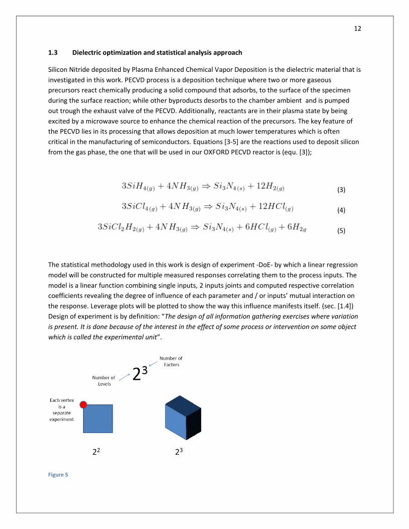
Total number of experiments will be 2416 different experiments. A graphical method to visualize the
method is in (fig. [5]); for a design with 2 degrees of freedom and 2 different inputs; total number of
experiments will be 4 that is each one can be represented by a square vertex. A design with 23 having 8
experiments in total will count for 8 vertices of a cube.
It is a strategy to gather empirical knowledge and it goes in the following pattern of steps:
[1]-Define objective for the investigation, which means, one should identify the target response that
should be optimized. For our experiment here, we seek optimizing the following output responses,
these which are listed by priority:
-Deposition Rate dH/dt
Our experiments should have deposition rates low enough to deposit 10 nm of silicon nitride in
such a way to allow reasonable amount of time for the Plasma state to be established and
stable. Otherwise, we either cannot get a comparable dimension or we won’t have a stable
deposition process which means that the results won’t be reproducible.
-Electrical characteristics: Film resistivity, dielectric constant and Breakdown voltage.
-Losses: Interfacial polarization including bulk “space charge” and interface traps.
-optical properties which shows chemical composition: refractive index
This parameter indicates how much silicon is incorporated in the composition of the non
stoichiometric silicon nitride; higher refractive index denotes higher mole content of silicon; it
shouldn’t be –however- an indicator of how good the nitride film is in the frame of our
application. Though it has been reported in [32] that higher silane to ammonia ratio which
includes more silicon in the film lowers the break down voltage of the nitride. It can be
attributed to the common dangling bond and silicon to silicon bond that could occur if there is
more than enough silicon in the plasma ambient. It has been further explained in [39] that Si-Si
antibonds forms donor traps near the conduction band of the SiN that carriers hop through from
the Schottky gate to the SiN/AlGaN interface acting as a leakage current medium through the
transistor and limiting the high frequency response of the device. Our experience and
measurements further assist this explanation, it has been shown that very good leakage and
2 Rigorous Mathematical background and software user guide, refer to [48] [49] [50]

14
breakdown behavior on GaN area diodes with very low Silane to ammonia ratio; this will be
shown in (sect. [5]).
Adding to these, composition stress, thermal expansion coefficient and density… but these are not as
much important as the previous ones.
[2]-Define variables that will be controlled during the experiment i.e. [design variables] and most
importantly their degree of variation, in other words their interval of variability; i.e. their maximum and
minimum shifts from a center point that was chosen based on previous researchers results. These are
the RF power, temperature, gas pressure and gases ratio.
[3]-Define the variable to be measured to describe the expected investigated response (#1) that should
be optimized i.e. [response variables] which are also called the experimental units; which could be for
example the resistivity measured across a Metal Insulator Metal structure, its capacity using CV
[capacitance vice voltage] and CF [capacitance vice frequency] measurements and stress measurement.
And most importantly find a method to draw a number that is representative of the measurement; it is
worth noting that the simulation software deals with one dimensional array of numbers with each
representing a response of only one experiment of the 16 not data sets or curves.
Actually the most tedious task is to define a reliable representative method to draw this number thus
characterizing the curve; in some instances as shown in (sect. [4.5]), the reliability of the measurement
and the testing tool is well established however, the characterization method is difficult or could lead to
drawing wrong conclusions.
1.4 Extracting the trends from JMP simulations
This section describes some of the terminologies used in the estimation theory that is the main statistical theory used by JMP to estimate the linear regression model, coefficients and in what way each input is involved in the output using leverage plots.
JMP fits the response into a linear regressed model ψ as a function of all the inputs pi (equ. [6]) where C0 is a constant, µi is the mean value of the input pi’s 2 extreme values (+1/-1) and δi is difference between these 2 values. αi and βi are the regression coefficients of the single input and the mutual input set respectively. The earlier reveals the single input influence and the latter reveals the mutual interaction between two inputs. The only setback of this method is that the model is linear thus it cannot predict nonlinear dependencies; and the prediction results may not be even valid in other input ranges.
(6)
15
The following terms are the most important for our purpose; each is shown in the simulation results (fig[7-8]); hence an explanation is necessary.
Parameter estimate: is the estimated coefficient in the liner regression function “αi and βi”
In estimation theory, an estimator “the algorithm used by JMP to construct the linear function” attempts to approximate the unknown parameters using the given measurement data. Loosely speaking, it is assumed that the desired information is to be extracted from a noisy signal or pool of data; noise thus adds uncertainty, that’s why estimation is needed to reduce the interval of confidence or else the problem would be deterministic and no estimation is required.
Standard error: is the estimate of the error in the standard deviation of the parameter estimate
t-ratio: is the parameter estimate divided by the standard error; “it is an estimate standardized by subtracting the hypothesized mean and dividing by the standard error. This is close to normal distribution except that the standard error is by itself estimated.” JMP explanation. A good reference value denoting high significance is a t-ratio with a value comparable or higher than 2 in absolute terms.
A leverage plot is a tool to show how an effect is significant compared to the null hypothesis. It gives more insight on how the regression curve fits the data. It is of importance because it tests each parameter’s significance on the output independently by comparing the residuals “the errors” in the fitting of the regression curve to the actual data between two cases:
-One is the case of the null hypothesis the other one is the case with the parameter considered as an influential effect in the regression equation (equ. [6])
In other words, it compares the two cases with the parameter included and with it removed.
Each point on the graph represent one experiment in the DOE; the distance of the point to the mean value “blue x axis (fig [8])” is what the residual would be with the effect removed; the x-axis represents the regressed model with the null hypothesis being true; in other words the hypothesized value of the parameter is zero. While the distance of the point to the sloped regression line is the actual residual of the regression that is with the effect being considered. The closer the points to the sloped fit line, than the mean line, means that the fitting actual residuals are less compared with the residuals predicted with the null hypothesis proving that the fitting with the effect included is more accurate and representative to the actual truth. In the DOE case with two degrees of freedom, the graph plots the points with the parameter first value (+1) to the right and the parameter second value (-1) to the left. Depending on the sign of the slope, the parameter influence is evaluated; that is if the slope is positive, this means that with the parameter having the (+1) value, the response is increased and vice versa for the negative slope case.
It is imperative to note that two effects might have a significant leverage on the response if analyzed independently but if combined, their leverage plot might reveal no influence at all; in other words, the fit line is parallel to the mean value line; this does not mean -however- that by combining the two, the latter cancels the influence of the first on the output but it means that the mutual interaction between the two is not a significant parameter in the regression model.

16
Figure 6
Figure 7
Figure 8

17
2. CVD OF SILICON NITRIDE
[1] Characteristics and Properties Silicon nitride (Si3N4) is an excellent electrical insulator and diffusion barrier (to sodium and water vapor) and has replaced CVD oxides in many semiconductor devices. It is found as an amorphous material or in two hexagonal crystalline forms, α and β, the latter being the high-temperature form. α transforms to β irreversibly at 1600 C. Some of its astounding properties include: • Light weight • High strength and toughness for tough ceramic applications • High chemical resistance to acids, bases, salts, and molten metals • Good resistance to oxidation up to 1500 C • High electrical resistivity Chemical Resistance Silicon nitride is resistant to oxidation up to 1350 C. It is resistant to most reagents at room temperature. [2] CVD Reactions One of the deposition reactions for silicon nitride amalgamates silicon tetrachloride (SiCl4) and ammonia (NH3): Reaction (1)
(4)
The optimum deposition temperature is 850°C. Pressure may be up to 1 atm. A hydrogen or nitrogen atmosphere is used with very high ratio of N2 to reactants (ca. 1000/1) Another reaction uses dichlorosilane (SiH2Cl2) with ammonia: Reaction (2)
(5)
The reaction that will be used to produce the silicon nitride subject of this work is (3)
Reaction (3)
(3)
In the OXFORD plasmalab 80, silane is diluted in N2 in a 2 to 98 gas mixture.
18
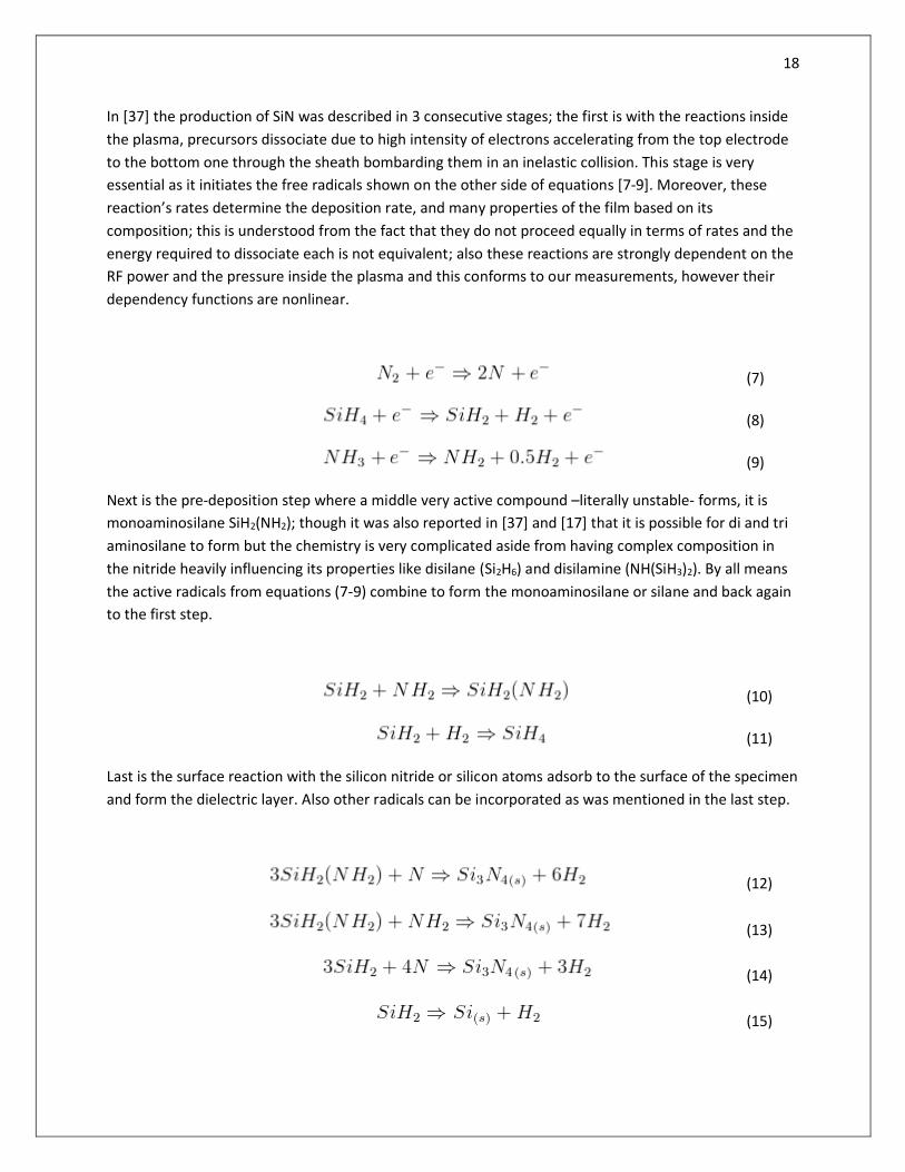
In [37] the production of SiN was described in 3 consecutive stages; the first is with the reactions inside
the plasma, precursors dissociate due to high intensity of electrons accelerating from the top electrode
to the bottom one through the sheath bombarding them in an inelastic collision. This stage is very
essential as it initiates the free radicals shown on the other side of equations [7-9]. Moreover, these
reaction’s rates determine the deposition rate, and many properties of the film based on its
composition; this is understood from the fact that they do not proceed equally in terms of rates and the
energy required to dissociate each is not equivalent; also these reactions are strongly dependent on the
RF power and the pressure inside the plasma and this conforms to our measurements, however their
dependency functions are nonlinear.
(7)
(8)
(9)
Next is the pre-deposition step where a middle very active compound –literally unstable- forms, it is
monoaminosilane SiH2(NH2); though it was also reported in [37] and [17] that it is possible for di and tri
aminosilane to form but the chemistry is very complicated aside from having complex composition in
the nitride heavily influencing its properties like disilane (Si2H6) and disilamine (NH(SiH3)2). By all means
the active radicals from equations (7-9) combine to form the monoaminosilane or silane and back again
to the first step.
(10)
(11)
Last is the surface reaction with the silicon nitride or silicon atoms adsorb to the surface of the specimen
and form the dielectric layer. Also other radicals can be incorporated as was mentioned in the last step.
(12)
(13)
(14)
(15)

19
Solid silicon -when created- consists a percentage in the film, this could increase the film’s refractive
index but will lower its breakdown voltage, the ohmic conduction region and increase leakage current
because of traps induced by Si-Si bonds, antibonds acting as hole acceptor states and electrons donor
states respectively [39], in addition to dangling bonds near [Si-H], [Si-N] and [N-H] bond groups.
The remaining problems in the process are:
-The non idealities in the process with possible high
hydrogen content from monoaminosilane, disilamine
and disilane content. If there is any Si dangling bonds,
near hydrogen atoms bonding to these compounds
modulates their electronegativity [33] ; i.e. the
energy of the trap or the energy of the quantum
trapping well, thus creating trap states with different
energy distributed along the whole bandgap.
-Non ideal vacuum in the chamber with small portion
of gas impurities like oxygen which can also bound to
the nitride radicals and form oxynitrides. This also
have the same effect in modulating the dangling
bonds but due to the higher electronegativity of the
oxygen, the trap state energy becomes more negative, the other way around is with hydrogen
impurities. However another step was added before vacuuming the chamber and beginning the
deposition process; which is venting the chamber with N2 gas which will combine with oxygen molecules
and form NO2 compounds and will be exhausted.
-Possibility of alkaline positive ions to diffuse through the nitride during any step in the processing, i.e.
rinsing or lift off
Dangling bonds are in principle common as defects because silicon nitride unfortunately has a marginal
structural flexibility to accommodate any random misplacement to the bonding angles
Figure 10
Figure 9

20
[3] Characteristics and Properties of Silicon Nitride Si3N4 has the same structure and orbital hybridization similar to CH4 (methane) (fig [9])
Figure 9-10 show the type of hybridization for each atom and the angles between bonds. The range of deposition temperature is 755–810 Celsius with a high dilution of nitrogen. With the high-frequency plasma (13.56 MHz), the deposition temperature is lower (400–600 Celsius) and this is where the plasma enhancement takes form. The ammonia-to-silane ratio should be greater than 10/1 to ensure proper stoichiometry since ammonia decomposes slower than silane; and this is what was followed in our experiments; the ratio of (SiH4 2% in N2) to NH3 to was form 0.333 to 1.25. In various deposition recipes, very bad composition of silicon nitride can be attained that contains up to 8 percent of Hydrogen atoms [7] bonded to both nitrogen and silicon. The tendency to have hydrogen in the film could be remedied by using nitrogen instead of ammonia: 3SiH4 + 2N2 → Si3N4 + 6H2
However, the nitrogen molecule has a far greater bonding energy than ammonia and is more difficult to dissociate into free atomic nitrogen active species. Consequently, the deposition rate is extremely slow. This can be offset by plasma activation with high frequency (13.56 MHz) or electron cyclotron resonance (ECR) plasmas and with microwave activation. The film deposited at these low temperatures (200-400 C) by PECVD is often not stoichiometric Si3N4 and
is often designated as just SiN or SixNy. In fact, even more hydrogen than in high temperature CVD is
there and the film is often referred to as SixNyHz.
The compound is generally not used in direct contact with silicon because of its relatively poor interface
with silicon substrates properties, especially with regard to fixed or interface trapped charges which
means a highly leaky structure and its high build up stress due to non matching lattice constants; this
was discovered in [4.4] as a leak mechanism in the MIM structures that were used leading to high loss
tangent measurements. This was solved by coating the Si substrate by a 360nm thick layer of silicon
dioxide beneath the MIMs array.

21
3.0 Theoretical Background
3.1 Plasma3
It has been shown in our results that the RF power is an essential factor in the deposition rate of the
PECVD nitride and its characteristics. The explanation of this correlation is linked to the “collision cross
section” another physical concept used in the description of the plasma mechanics instead of the
collision frequency or collision probability. A glimpse into the theoretical aspects of plasma, some of its
main governing laws and its most common features will be presented in this section
In physics, plasma is a partially ionized gas, in which a certain proportion of electrons are free rather
than being bound to an atom or molecule. The ability of the positive and negative charges to move
somewhat independently makes the plasma electrically conductive so that it responds strongly to
electromagnetic fields. Plasma therefore has properties quite different of solids, liquids, or gases and is
considered to be a distinct state of matter. Like gas, plasma does not have a definite shape or a definite
volume unless enclosed in a container; unlike gas, in the influence of a magnetic field, it may form some
of its weirdest and intriguing phenomenonal structures such as filaments, beams and double layers.
Plasma Energy
Is a non thermal form of energy. With the RF source, gas molecules ionize and enough active radicals are created to enhance the chemistry of the reaction between the precursor gases to deposit the required layer on the substrate at lower temperatures. The ambient contains all forms of electrically charged or uncharged particles: electrons, ions, neutral molecules and radicals. Free radicals are from an electrical point of view; neutral species having incomplete bonding and are extremely reactive; they are within the ambient hunting for another free radical to bond with and form a stable molecule. As was shown previously in the chemistry of silicon nitride (sect [2]) that for the nitride to result, there should be a middle step where monoaminosilane or higher orders of radicals must exist first before the surface reactions and because of their instability, they are highly reactive and will most likely dissociate or bond with another radical and form either the nitride or the byproduct gas or can even be incorporated in the film with other forms like disilamine and disilane.
The net result from the fragmentation, the free radicals, and the ion bombardment inside the plasma is that the surface processes and deposition occur at much lower temperatures than in non-plasma systems which is desired.
3 For rigorous mathematical treatment, refer to [3][5]
22
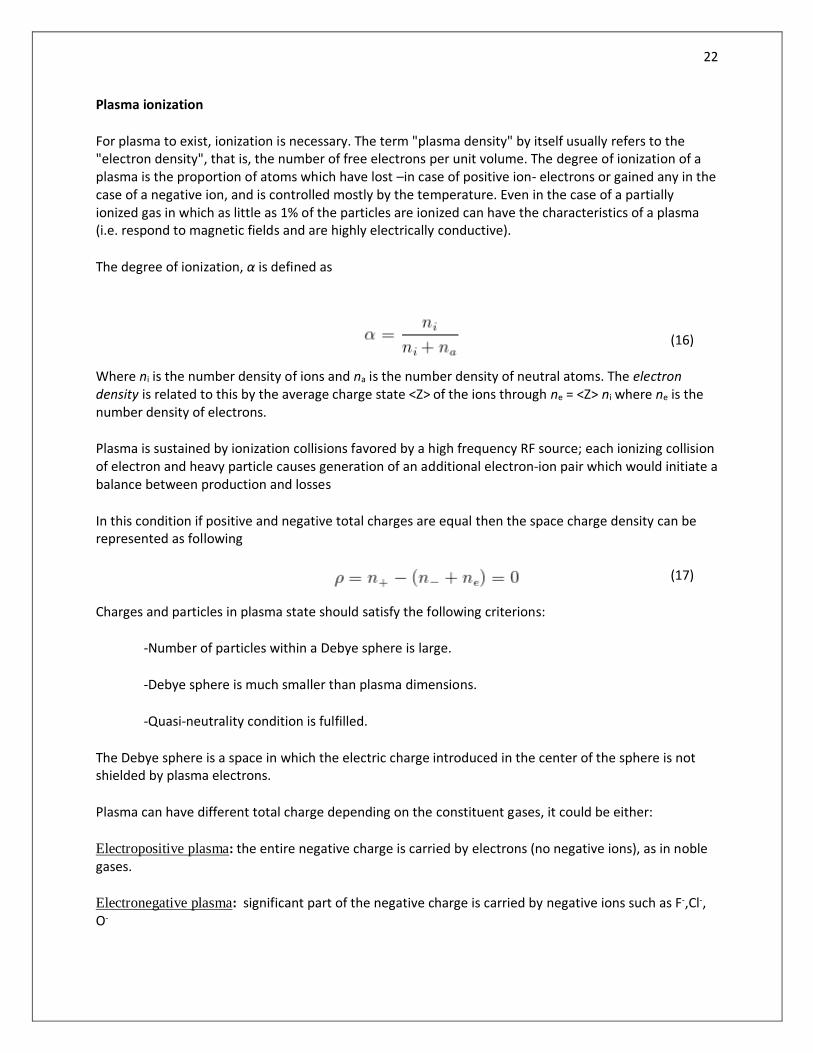
Plasma ionization
For plasma to exist, ionization is necessary. The term "plasma density" by itself usually refers to the "electron density", that is, the number of free electrons per unit volume. The degree of ionization of a plasma is the proportion of atoms which have lost –in case of positive ion- electrons or gained any in the case of a negative ion, and is controlled mostly by the temperature. Even in the case of a partially ionized gas in which as little as 1% of the particles are ionized can have the characteristics of a plasma (i.e. respond to magnetic fields and are highly electrically conductive).
The degree of ionization, α is defined as
(16)
Where ni is the number density of ions and na is the number density of neutral atoms. The electron density is related to this by the average charge state <Z> of the ions through ne = <Z> ni where ne is the number density of electrons.
Plasma is sustained by ionization collisions favored by a high frequency RF source; each ionizing collision of electron and heavy particle causes generation of an additional electron-ion pair which would initiate a balance between production and losses
In this condition if positive and negative total charges are equal then the space charge density can be represented as following
(17)
Charges and particles in plasma state should satisfy the following criterions:
-Number of particles within a Debye sphere is large.
-Debye sphere is much smaller than plasma dimensions.
-Quasi-neutrality condition is fulfilled.
The Debye sphere is a space in which the electric charge introduced in the center of the sphere is not shielded by plasma electrons.
Plasma can have different total charge depending on the constituent gases, it could be either:
Electropositive plasma: the entire negative charge is carried by electrons (no negative ions), as in noble gases.
Electronegative plasma: significant part of the negative charge is carried by negative ions such as F-,Cl-, O-
23
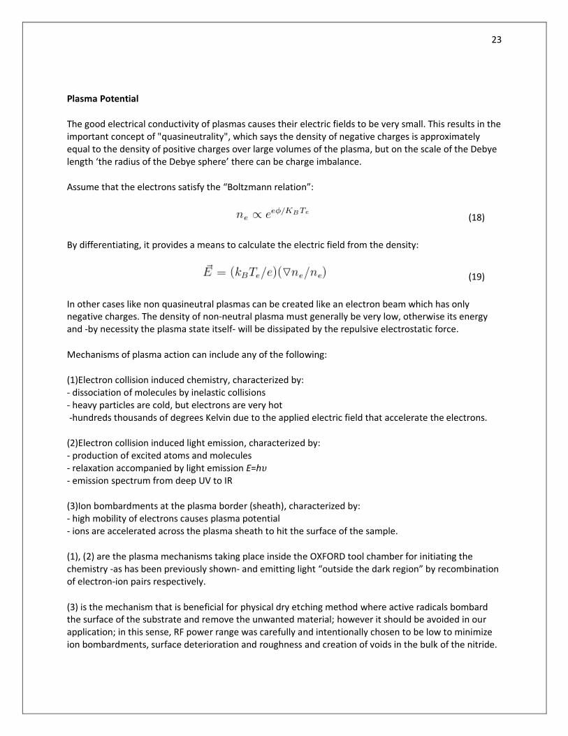
Plasma Potential
The good electrical conductivity of plasmas causes their electric fields to be very small. This results in the important concept of "quasineutrality", which says the density of negative charges is approximately equal to the density of positive charges over large volumes of the plasma, but on the scale of the Debye length ‘the radius of the Debye sphere’ there can be charge imbalance.
Assume that the electrons satisfy the “Boltzmann relation”:
(18)
By differentiating, it provides a means to calculate the electric field from the density:
(19)
In other cases like non quasineutral plasmas can be created like an electron beam which has only negative charges. The density of non-neutral plasma must generally be very low, otherwise its energy and -by necessity the plasma state itself- will be dissipated by the repulsive electrostatic force.
Mechanisms of plasma action can include any of the following:
(1)Electron collision induced chemistry, characterized by: - dissociation of molecules by inelastic collisions - heavy particles are cold, but electrons are very hot -hundreds thousands of degrees Kelvin due to the applied electric field that accelerate the electrons.
(2)Electron collision induced light emission, characterized by: - production of excited atoms and molecules - relaxation accompanied by light emission E=h𝜐 - emission spectrum from deep UV to IR
(3)Ion bombardments at the plasma border (sheath), characterized by: - high mobility of electrons causes plasma potential - ions are accelerated across the plasma sheath to hit the surface of the sample.
(1), (2) are the plasma mechanisms taking place inside the OXFORD tool chamber for initiating the chemistry -as has been previously shown- and emitting light “outside the dark region” by recombination of electron-ion pairs respectively.
(3) is the mechanism that is beneficial for physical dry etching method where active radicals bombard the surface of the substrate and remove the unwanted material; however it should be avoided in our application; in this sense, RF power range was carefully and intentionally chosen to be low to minimize ion bombardments, surface deterioration and roughness and creation of voids in the bulk of the nitride.
24
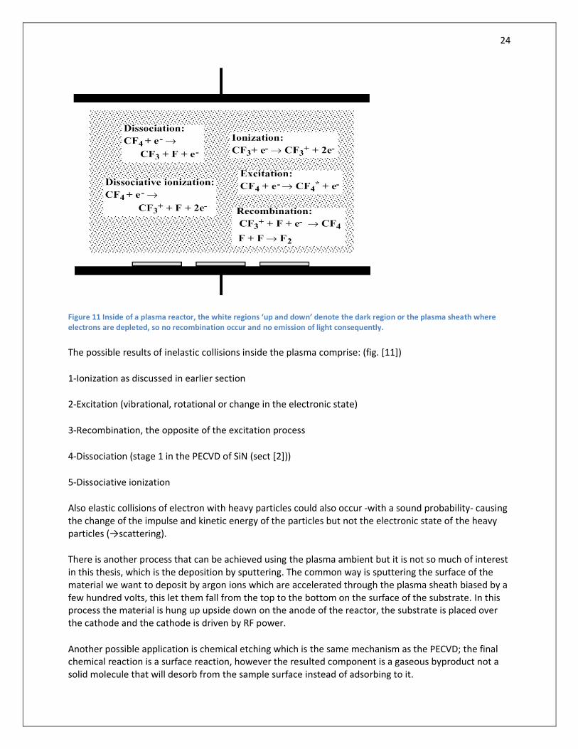
Figure 11 Inside of a plasma reactor, the white regions ‘up and down’ denote the dark region or the plasma sheath where electrons are depleted, so no recombination occur and no emission of light consequently.
The possible results of inelastic collisions inside the plasma comprise: (fig. [11])
1-Ionization as discussed in earlier section
2-Excitation (vibrational, rotational or change in the electronic state)
3-Recombination, the opposite of the excitation process
4-Dissociation (stage 1 in the PECVD of SiN (sect [2]))
5-Dissociative ionization
Also elastic collisions of electron with heavy particles could also occur -with a sound probability- causing the change of the impulse and kinetic energy of the particles but not the electronic state of the heavy particles (→scattering).
There is another process that can be achieved using the plasma ambient but it is not so much of interest in this thesis, which is the deposition by sputtering. The common way is sputtering the surface of the material we want to deposit by argon ions which are accelerated through the plasma sheath biased by a few hundred volts, this let them fall from the top to the bottom on the surface of the substrate. In this process the material is hung up upside down on the anode of the reactor, the substrate is placed over the cathode and the cathode is driven by RF power.
Another possible application is chemical etching which is the same mechanism as the PECVD; the final chemical reaction is a surface reaction, however the resulted component is a gaseous byproduct not a solid molecule that will desorb from the sample surface instead of adsorbing to it.

25
3.2 Collision Cross Section
The collision cross section is a descriptive concept for the probability of having a collision between 2 particles; it is a measure of how probable or effective a collisional interaction would be between a projected particle and a certain target. The larger the cross section, the more plausible the interaction will occur. A cross section stands for the total surface area of the target atoms in a unit volume; in other words, it represents the effective area of the collision. It depends on the density of the ambient and the velocity, the faster the projected particle is the larger is the probability to scatter or interact in any other form; consequently the larger is the cross section. The density and the velocity are directly linked to the pressure and the RF power. This quantity can also be linked by the notion of the mean free path which is the distance departed by the particle between 2 consecutive collisions; the more collisions there are, the larger is the cross section and the shorter is the mean free path. The collision cross section is a necessary concept in explaining the measured results since the first step in the chemistry is dissociative collisions. It shall be shown that with higher RF power we have more collisions and higher deposition rate but if high enough the plasma could deteriorate the surface of the film and introduce spacial defects in the layer.
The collision frequency 𝜈 defined as the number of collisions per unit time corresponds to the number of particle centers present in a cylinder swept by a circle with area s during one time unit and the area s is the collision cross section with its diameter called the collision diameter. Knowing the concentration of particles n and the collision cross section; the collision frequency can be expressed by: n*𝜎*∆x and where ∆x is an infinitesimal displacement and dividing by unit time, we get:
The mean free path is the distance covered by a particle on average between two collisions, it is the collision frequency divided by the particle velocity v
(20)
Following are different experimental measurements done during the sixties and seventies to relate the different collision mechanisms’ cross sections of different gases with energy which is the RF source in our application; only for giving a general idea. It is notified that always the function rises and have a peak value then at a certain point, it will have to go down really fast where the density of collisions is so much that the scattering has completely gone on an insane track, the mean free path gets extremely short and then the surface of the specimen can be deteriorated; however, in our number limits: 15 to 45 watts the collision cross sections of the dissociation of the silane and the ammonia increases with increasing the power. This is justified by the JMP statistical simulations.
26
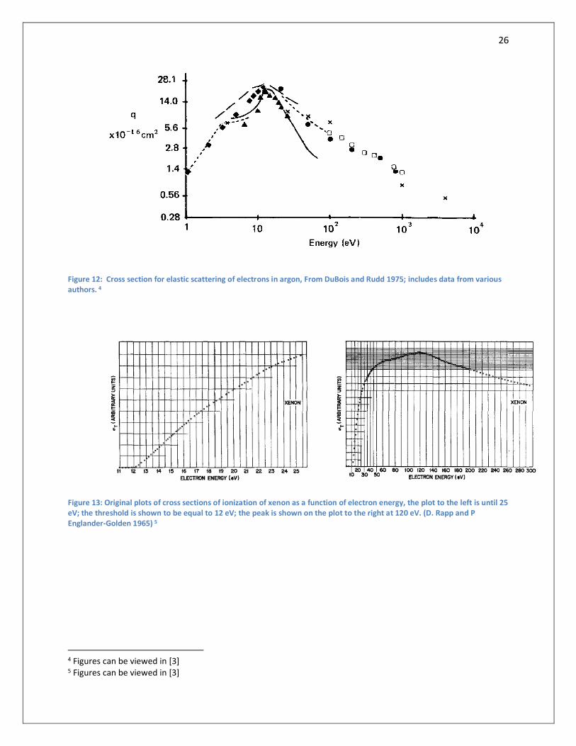
Figure 12: Cross section for elastic scattering of electrons in argon, From DuBois and Rudd 1975; includes data from various authors. 4
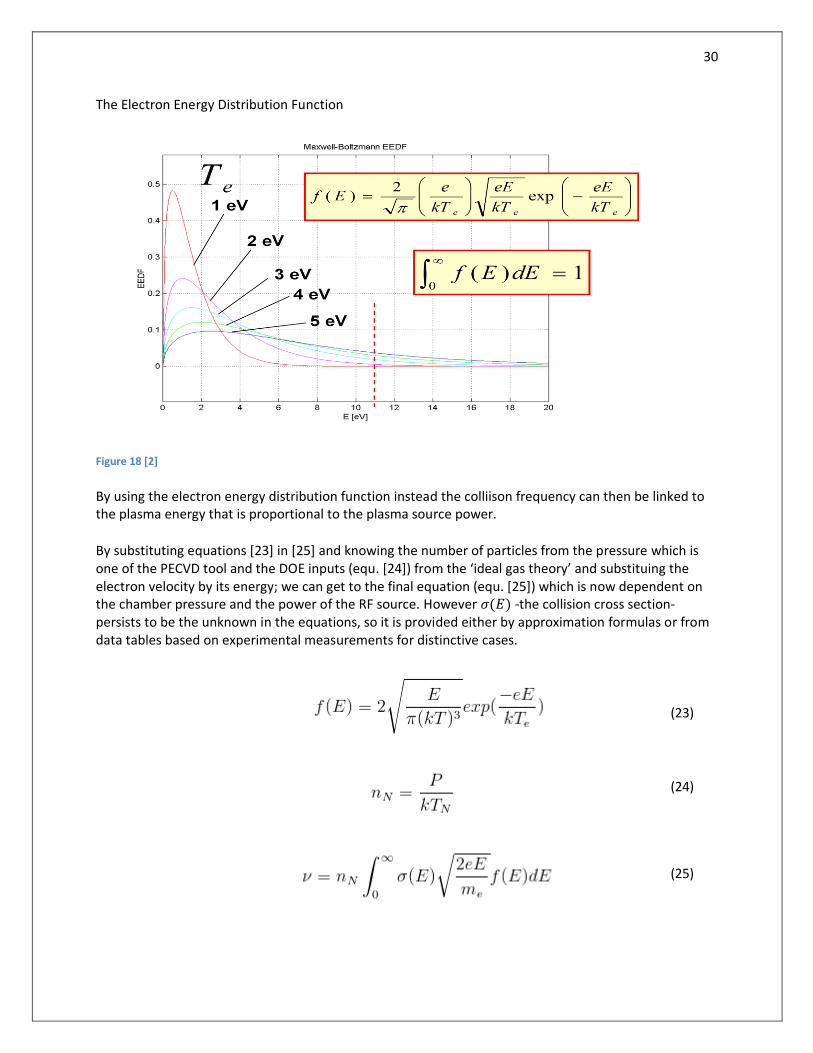
Figure 13: Original plots of cross sections of ionization of xenon as a function of electron energy, the plot to the left is until 25 eV; the threshold is shown to be equal to 12 eV; the peak is shown on the plot to the right at 120 eV. (D. Rapp and P Englander-Golden 1965) 5
4 Figures can be viewed in [3] 5 Figures can be viewed in [3]

27
Figure 14: Ionization cross-sections of the noble gases (From Rapp and Englander-Golden 1965; includes data from (S) Smith 1930 and (SWHK) Schram et al. 1965. Similar values for Ar, He and Ne have been obtained by Fletcher and Cowling 1973); n.b.𝝅a2 = 8.82*10-17cm2
Note also to that the graph is not given in units of squared centimeter; rather it is in 𝜋a2 the area of the circle with radius is the Bohr radius of hydrogen.

28
Figure 15: Excitation cross sections for the 2p levels of Ne atoms (I. P. Zapesochnyi and P. V. Fel’tsan 1967)
Figure 16: Cross section of dissociative ionization – absolute cross sections and the fraction of the total ionization are plotted on each graph.(Rapp, Englander and Briglia 1965)

29
As previously stated, the collision frequency can be represented as in (equ. [21])
(21)
The collision cross section is velocity dependent; i.e. the total probability of collision has to be summed
up over the infinite distribution of particle velocities putting into consideration the probability
distribution of velocities in the ambient of the plasma which can ideally follow a Maxwell Boltzmann
distribution as shown in (fig. [17]). In this case, the collision frequency is then formulated as in (equ [22])
(22)
Maxwell Boltzmann
Figure 17 Maxwell Boltzmann Distribution showing the velocity dependent distribution function f(ve) with the 3 dimensional average velocity computed and the velocity of each degree of freedom. [2]
It is then easy to transform the velocity dependent distribution to an energy dependent distribution, by
considering the kinetic energy of the particles. Then we can arrive to the EEDF (fig. [18])
30
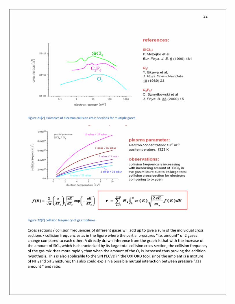
The Electron Energy Distribution Function
Figure 18 [2]
By using the electron energy distribution function instead the colliison frequency can then be linked to the plasma energy that is proportional to the plasma source power.
By substituting equations [23] in [25] and knowing the number of particles from the pressure which is one of the PECVD tool and the DOE inputs (equ. [24]) from the ‘ideal gas theory’ and substituing the electron velocity by its energy; we can get to the final equation (equ. [25]) which is now dependent on the chamber pressure and the power of the RF source. However 𝜎(𝐸) -the collision cross section- persists to be the unknown in the equations, so it is provided either by approximation formulas or from data tables based on experimental measurements for distinctive cases.
(23)
(24)
(25)

31
If we substitute in the ionization collision frequency function (fig [19]) from the table with all the constants and solve for the integral, the ionization cross frequency can be then computed as (fig [19]). The same is done for the excitation case with the same gas. It is clear that both results do not yield the same cross sections, then obviously not the same collision frequency and not the same occurrence probability.
Figure 19[2] the electron energy distribution function and the ionization cross section for a He gas
Figure 20[2] the electron energy distribution function and the excitation cross section for a He gas
32
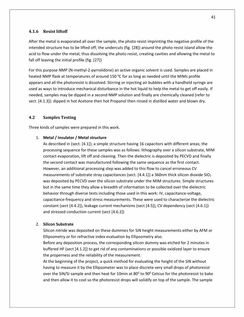
Figure 21[2] Examples of electron collision cross sections for multiple gases
Figure 22[2] collision frequency of gas mixtures
Cross sections / collision frequencies of different gases will add up to give a sum of the individual cross sections / collision frequencies as in the figure where the partial pressures “i.e. amount” of 2 gases change compared to each other. A directly drawn inference from the graph is that with the increase of the amount of SiCl4 which is characterized by its large total collision cross section, the collision frequency of the gas mix rises more rapidly than when the amount of the O2 is increased thus proving the addition hypothesis. This is also applicable to the SiN PECVD in the OXFORD tool, since the ambient is a mixture of NH3 and SiH4 mixtures; this also could explain a possible mutual interaction between pressure ”gas amount ” and ratio.

33
3.3 Deposition techniques
Different deposition methods do exist for different material films. Table [2] and table [3] outline
the most common methods used for these films, along with their reactions if the deposition is
chemical and their corresponding conditions.
PECVD traits:
Glow-Discharge
Plasma Type Non-Isothermal (non-equilibrium)
Frequency 13.56 MHz
Power 1–100 kW
Flow rate measured in sccm
Electron concentration 109–1012/cm3
Pressure 1mTorr to 1000mTorr
Electron temperature ~104 K varies according the RF source power.
Atom temperature ~104 K
It is worth noting that the sccm “standard cubic centimeter” refers to a unit to measure the
throughput or flow rate of gases inside the reactor chamber, it is standard because it measures
this quantity in standard temperature 0 Celsius and standard pressure 1 atmosphere or 760 torr
1sccm=6.022*1023 molecules per minute
Table 2 adapted from [2]

34
Table 3 adapted from [2]
These are the main steps –excluding any complex mechanisms or reactions- of the PECVD (fig.[23])
Figure 23
1. Transport of reactants by forced convection to the deposition region 2. Diffusion through the boundary layer to the wafer surface 3. Adsorption of reactants on the wafer surface 4. Surface processes (Decomposition, migration, attachment, …) 5. Desorption of byproducts from the wafer surface 6. Diffusion of byproducts through the boundary layer to the main gas stream 7. Transport of byproducts by forced convection from the deposition region

35
A necessary assumption in the analysis of the results in general; -specifically- the deposition rate and for simplicity is that the PECVD process is a linear time invariant system. This work’s results have shown this is not the case; in the first series of deposited nitrides 10 nm was not achieved, consequently the height was measured and the required time for the 10nm thickness was calculated based on the linearity assumption; however after measurements of the second series, it was confirmed that the assumption is wrong; but still it can be applied more or less with a certain degree of inaccuracy to adjust the expected deposited height. Moreover the assumption has to be made since the JMP fitting calculations regress the deposition rate dependencies on power and pressure using a linear model and since power is the source energy per time then the regression model holds the time dependency to be linear. Results then cannot be interpreted unless this assumption is a priori. But still, physically the assumption is wrong; it has been explained by theory that a simple deposition process–not taking into consideration non linear plasma mechanics and complex chemistry- the growth velocity is dependent on local pressure, deposition temperature, reactor geometry and source power.
Figure 24[2]
So particles moving towards a specimen surface can be characterized by their concentration gradient CG which decreases the closer to the specimen (fig [24]) and by the surface concentration CS. F1 and F2 are the “thrust” forces; F1 is carrying the particles by convection or diffusion through the plasma ambient and F2 is responsible for all surface reaction (attachment or adsorption). They must in principle be equal to satisfy a continuity condition.
If (26) then it follows that (27)
(Equ [27]) can be written as (28)
Then in (26) it follows from (28) that
(29) (30)

36
Dividing F (equ [29]) “the surface force; i.e. the force per unit surface area” by N “number of particles in a unit volume” we get the rate of change of the third dimension perpendicular to the surface which is the deposition height. The final deposition rate is adjusted to count for lower or fractional gas pressures i.e. less volumetric density of gas molecules (equ [31]). Depending on the difference of the mass transfer coefficient compared to the surface reaction constant the deposition process will be governed by the lowest value of either; i.e. the growth rate will be mass transferred controlled or reaction controlled.
(31)
Figure 25[2] DG is dependent on the RF source power, then if the reaction is mass transfer controlled, the deposition rate would be likewise dependent on the source power.
Figure 26[2]
In the case of lowering the pressure in the reactor to levels around 500m Torr, this equation has to be altered in a way to emphasize the change in the gas transfer coefficient; this coefficient is dependent on diffusivity which is inversely proportional to the number of collision between the reactant particles: ions, radicals and electrons which are much hotter than the ions by
several thousand degrees Kelvin due to the electric field induced in the PLASMA.

37
4.0 Experimental work
4.1 Processing of Samples
The experimental procedure involved choosing a cheaper and easier sample structure –less in
processing steps; i.e. cheaper to manufacture- to optimize, and study the dielectric instead of
manufacturing the complete transistor structure involving over 15 different steps or more. The sample
used was structured in the form of an array of capacitors with 16 possible areas (fig. [28]). Capacitors
were formed with the overlap of two metal contacts with the insulator in between. Length of contacts
were nearly kept at 500 µm with their width being 50, 100, 125, 150 µm consecutively; and through the
permutation of these dimensions between the top contact and the bottom contact, 16 different areas
were possible. The substrate that was used was (100) p type silicon with doping on the order of
1013cm-3. However, this substrate had to be coated with 360 nm thick of silicon dioxide to have reliable
C-V measurements through preventing the creation of a depletion region in the silicon and measure
additional stray capacitances of the channel of a MIS structure. (Section [4.4])
Figure 27 Red areas are the capacitors formed by the overlap of 2 contacts with the dielectric in between. The contact were Gold 200nm / Titanium 50nm
50µm
100µm
125µm
150µm

38
This structure was manufactured by lithography for bottom contact arrays, evaporation of metal
contact, mask lift off. Samples were cleaned then silicon nitride was deposited by PECVD. Finally the
same procedure for the bottom contact was followed for the upper contact.
In addition to the MIM (metal / insulator / metal) structures, other samples with silicon nitride
deposited on silicon substrates and titanium nitride substrates were manufactured for other
characterization measurements.
The processing steps involved PECVD, wet etching, chemical cleaning, optical lithography, evaporation
of metallic contacts and lift off.
4.1.1 PECVD
The plasma enhanced chemical vapor deposition was done with a load locked OXFORD plasmalab 80
with gases being fed with a shower head and the sample placed on a hot carrier table. Gases used were
ammonia (NH3), silane (SiH4) (2% diluted in N2), and nitrogen (N2). An automatic pressure control valve
(APC) hooked to the chamber is responsible to control the chamber pressure with a proportional
integral differential (PID) circuit controlling the open section of the valve ; the pressure data are
measured with a sensitive capacitance manometer. The plasma excitation source is a radio frequency
source oscillating at 13.56 MHz with an auto match unit (AMU) with controlled variable capacitors
attached. The table heater and the mass flow are also controlled by a PID controller. The whole system
is controlled with a programmable logic controller (PLC) a Graphical User Interface (PC 2000).
All recipes -but not including cleaning- for the deposition process consist of the following steps:
[1] After the sample is placed on the table and the chamber is closed, a vacuum pump sucks the air
inside the chamber until pressure reaches 6 to 8 mTorr, and then the exhaust valve is closed.
[2] Ammonia and Silane valves open up and (MFCs) mass flow controllers adjust the flow to the
amounts specified by the user.
[3] Chamber pressure is adjusted by the automatic pressure valve that opens accordingly; as soon
as the aspired value is reached, the RF power source is turned on and plasma state is created. If
the actual table temperature is not within the specified temperature margin of error which is +/-
10 degrees Celsius, the power source is not activated.
[4] When the deposition time elapses, the source turns off, ammonia and silane valves close while
the nitrogen valve opens up and purges the chamber with pressure of 1000 mTorr for 60
seconds.
[5] Finally for the chamber to open up for the samples to be extracted, gases are exhausted and
chamber is ventilated for 200 seconds.
Any deposition process from the 16 experiments has followed this scheme but only with different
input values for RF power, pressure, temperature, and gas flows. Moreover, the deposition of silicon
dioxide over the silicon substrate for the improvised MIM structures followed the same sequence in
deposition.

39
4.1.2 Wet etching
This procedure was used for etching the silicon nitride when the deposition height had to be evaluated
to calculate the deposition rate. Also, just prior to any deposition of silicon nitride on silicon substrates
for height or refractive index measurements by ellipsometry; each silicon substrate sample was etched
to get rid of any residual oxide layers or contaminants.
The process involved dipping the sample in buffered hydrofluoric acid (B-HF) for 2 minutes then
thoroughly rinsing in distilled water. The samples are then blown dry.
4.1.3 Chemical Cleaning
Samples were cleaned thoroughly before each deposition process by chemical cleaning. Additionally,
this step was used after liftoff to clean any metal, acid or for dissolving photo resist for height
measurements (sect. [4.2]). It involved dipping samples in a heated flask with Acetone solution for
approximately 5 minutes at a temperature of about 150 degrees. Then they are quickly placed in
another heated flask with Propanol solution also at 150 degrees for 5 minutes. Then finally samples are
rinsed in distilled water rotating rinsing unit and then blown dry.
4.1.4 Optical lithography [41]
Using the optical lithography, the metallic structure in (fig [27]) is transferred from the mask to the
substrate in two steps; one for the top contact and one for the bottom; both steps are necessarily the
same. Image reversal lithography was used for this purpose; to coat samples with photoresist where
metal is not desired to occur. The metal is evaporated on the photoresist which is then dissolved in NMP
so at the end the desired profile remains after liftoff and cleaning. In other words, a negative image
photoresist coat is imprinted on the samples and then lifted to leave the positive image metallic imprint.
The process begins with placing a sizeable amount of negative photoresist (AZ 5214E) drops on the
surface of the sample, which is then spun at 5000 rpm to ensure the even distribution and the
conformity of the resist thickness on the sample. During the spinning, the liquid coat tends to flow to
the boundaries because of the centrifugal force, thus forming a boundary layer of increased thickness.
To solve this, a soaked swab with photoresist resist dissolver (AZ EBR) was swept manually along the
boundary of the sample. After the coat is insured to be even, samples were prebaked at 900C for 120 sec
to harden the photoresist. Following is the sample exposure through the inverted mask “where the dark
areas follow the pattern expected to be deposited” to a UV source (fig [28]). The exposed area is now
soluble in the developer as would behave an exposed positive resist. But then samples are baked again
at 1150C for 120 sec for what is known as “reversal bake” that renders the exposed area which was
earlier soluble to be inert to light exposure while unexposed area still remains photo active. Now
samples are exposed to flood with no mask with power of around 275mJ/cm2. Finally they are
developed with the solution MIF 726 for 40 seconds with the samples placed on a rotating cylindrical
puddle. After development, the corresponding areas to the dark regions on the mask have no resist on
them while the others that should have no metal have photoresist with a sensible undercut for the lift-
off acid to flow underneath the metal after evaporation to dissolve the photoresist, then create a cavity

40
by which to allow the metal to fall off during cleaning. The whole exposure process was done on a
manual mask aligner with a 1000 watts mercury UV light.
Figure 28 Image reversal lithography method
4.1.5 Metal evaporation [41]
Following a lithography done for a MIM sample, the metal should be evaporated on the sample surface.
It is already known from the function of the lithography that after the evaporation and a lift off, an
equivalent picture of the mask will be transferred to the metal on the sample; that is where no metal
should be, photo resist will be occupying this region. For the MIMs, Ohmic contacts were evaporated;
they consist of 200nm of gold -for its high conductivity- on top of 50nm of titanium. Gold was
evaporated by thermal energy while titanium was evaporated by an e-beam. Each metal is placed in a
single tray by itself with a shutter; that opens only when this metal is being deposited. The sample is
hung upside down on a table that turns to adjust the sample position to the metal source at the time of
deposition. The evaporation tool used was Pfeiffer Classic 500L. Vacuum was required to be established
before any deposition takes place; pumps are turned on and stay pumping out for nearly 2 hours until
the room pressure would be on the order of 10-6 mbar. Maxtek MDC 360C a thin film averaging
controller controls the power of the e-beam or the thermal source during deposition to ensure the right
thickness is achieved.
41
4.1.6 Resist liftoff
After the metal is evaporated all over the sample, the photo resist imprinting the negative profile of the
intended structure has to be lifted off; the undercuts (fig. [28]) around the photo resist island allow the
acid to flow under the metal, thus dissolving the photo resist, creating cavities and allowing the metal to
fall off leaving the initial profile (fig. [27])
For this purpose NMP (N-methyl-2-pyrrolidone) an active organic solvent is used. Samples are placed in
heated NMP flask at temperatures of around 150 0C for as long as needed until the MIMs profile
appears and all the photoresist is dissolved. Stirring or injecting air bubbles with a handheld syringe are
used as ways to introduce mechanical disturbance in the hot liquid to help the metal to get off easily. If
needed, samples may be dipped in a second NMP solution and finally are chemically cleaned (refer to
sect. [4.1.3]): dipped in hot Acetone then hot Propanol then rinsed in distilled water and blown dry.
4.2 Samples Testing
Three kinds of samples were prepared in this work.
1. Metal / Insulator / Metal structure
As described in (sect. [4.1]); a simple structure having 16 capacitors with different areas; the
processing sequence for these samples was as follows: lithography over a silicon substrate, MIM
contact evaporation, lift off and cleaning. Then the dielectric is deposited by PECVD and finally
the second contact was manufactured following the same sequence as the first contact.
However, an additional processing step was added to this flow to cancel erroneous CV
measurements of substrate stray capacitances (sect. [4.4.1]) a 360nm thick silicon dioxide SiO2
was deposited by PECVD over the silicon substrate under the MIM structures. Simple structures
but in the same time they allow a breadth of information to be collected over the dielectric
behavior through diverse tests including those used in this work: IV, capacitance-voltage,
capacitance-frequency and stress measurements. These were used to characterize the dielectric
constant (sect [4.4.2]), leakage current mechanisms (sect [4.5]), CV dependency (sect [4.6.1])
and stressed conduction current (sect [4.6.2])
2. Silicon Substrate
Silicon nitride was deposited on these dummies for SiN height measurements either by AFM or
Ellipsometry or for refractive index evaluation by Ellipsometry also.
Before any deposition process, the corresponding silicon dummy was etched for 2 minutes in
buffered HF (sect [4.1.2]) to get rid of any contaminations or possible oxidized layer to ensure
the properness and the reliability of the measurement.
At the beginning of the project, a quick method for evaluating the height of the SiN without
having to measure it by the Ellipsometer was to place discrete very small drops of photoresist
over the SiN/Si sample and then heat for 10min at 800 to 900 Celsius for the photoresist to bake
and then allow it to cool so the photoresist drops will solidify on top of the sample. The sample

42
is then etched by buffered HF which will etch the uncovered SiN but not that which is under the
photoresist. The sample is then cleaned in hot acetone then hot propanol (sect [4.1.3]); the hot
acetone will dissolve the photoresist and will finally leave elevated –when compared to the
silicon surface- SiN profiles that were not etched by the B-HF. The height is then measured by
DEKTAK profilerometer if the feature height was above 30nm or an AFM for shallower features.
3. Titanium Nitride substrates
Silicon nitride was also deposited on TiN substrates as a way to measure the depolarization
currents that are caused by bulk trapped charges. The measurement was performed with an
MDC mercury profiler that uses clean mercury to establish an instantaneous dot/ring contact to
the sample thus saving the time and cost of manufacturing processes to manufacture the MIMs.
The mercury profiler was connected to the HP 4145B semiconductor analyzer to measure this
current. Moreover, TiN was chosen because it was noted in other results that SiN and TiN form a
very good interface; and this is desirable because the response that was to be evaluated is only
dependent on the silicon nitride bulk states and shouldn’t be dependent on the interface like in
the case of SiN over Si or measuring the depolarization current from MIM structures which will
be extremely affected by the contact sharp edges and electric field irregularities.
Characterization Tools:
- HP semiconductors analyzer 4145B for current and stress measurements
- HP/Agilent 4192 impedance analyzer for CV / CF measurements
- Karl Suss 4-probe station with a vacuumed chuck
- MDC mercury probe
- DEKTAK profilerometer
- Atomic Force Microscope
- Helium neon Laser ellipsometer

43
Prior to performing the 16 experiments, the two values of each parameter should be chosen in a way to
comply with the PECVD tool accuracy limits and considering the priority that the deposition rate of the
process should be as low as possible for stable operation and results reproducibility. A center point
(table [6]) was chosen with a small ratio for this purpose. In [32] it was shown that the deposition rate
scales with the ratio, so a small ratio was chosen in favor of higher RF power and longer deposition
times to achieve the 10nm feature thickness.
By contrast to previous work of the institute’s group, lower RF power or small time intervals had to be
chosen for the height to be comparable to 10nm, although the heights attained were still larger than 10.
The standard process (table [4], [5]) was usually achieving a refractive index of 2.0; that’s an indication
of higher silicon content which is not desirable for electrical parameters. It has been explained and
shown in [39] that higher silicon content lowers the Ohmic conduction limit and lowers the breakdown
voltage dramatically. The non stoichiometric nitrides processed for this work achieved refractive indices
between 1.75 and 1.85 which is definitely lower than the stoichiometric silicon nitride that should be
around 2.1 or higher. These refractive indices show lower silicon abundance in the nitride and explain
many of its superior electrical properties like higher break down voltage and low leakage.
Figure 29 the AFM scan of the center point sample with measured height of 16.0nm
Figure 30 profile step of center point sample; 16nm

44
The center point was processed then photoresist drops were placed on the sample, baked and solidified
“as was explained in (sect [4.2.2])” The SiN was etched in B-HF and the photoresist was cleaned in
Acetone/Propanol. And finally the high features were scanned by the AFM and leveled; the calculated
height was 16nm with 4 minutes deposition time (fig [29] [30]). Based on the center point, the (+1)/ (-1)
values were roughly assigned and the 16 samples were ready for processing. All the 16 SiN deposition
recipes were then processed on Si substrates as a first iteration and the height was evaluated by
ellipsometry to find the deposition rate and estimating the time needed for reaching 10nm for all of the
samples taking the linear dependency of the deposition process on time as a valid assumption. When
the final deposition times were calculated, the 16 elements of the set were processed in the second
iteration; but this time with the three substrates/structures intended in the plan of the characterization
techniques “MIMs, Silicon substrate and Titanium Nitride substrates”
Std SiN RF power SiH4 NH3 Pressure Temperature Time Thickness
passivation 10W 980 sccm 20 sccm 1000mTorr 300 0C 10 min 120 nm
passivation 10W 980 sccm 20 sccm 1000mTorr 300 0C 5 min 70.8 nm
passivation 10W 980 sccm 20 sccm 1000mTorr 300 0C 3 min 42.1 nm passivation 10W 980 sccm 20 sccm 1000mTorr 300 0C 2 min 27.7 nm
passivation 10W 980 sccm 20 sccm 1000mTorr 300 0C 1:30 min 20.8 nm
passivation 10W 980 sccm 20 sccm 1000mTorr 300 0C 1 min 15 nm passivation 6W 980 sccm 20 sccm 1000mTorr 300 0C 2 min 17.2 nm Table 4 standard process in depositing SiN
SiN RF power SiH4 NH3 Pressure Temperature Time Thickness
Gate dielectric
3W 268 sccm 4 sccm 540mTorr 320 0C 2:15 min 14 nm
Table 5 old recipe for SiN as gate dielectric
-1
Center Point 1
RF power 15W 30W 45W
Temp 250 0C 300 0C 350 0C
Pressure 250 mTorr 450 mTorr 650 mTorr
SiH4 17sccm 20sccm 36sccm
NH3 50sccm 30sccm 29sccm
ratio 0.333 0.66 1.25
TIME 4:30s 4s 1:35s Table 6
The total flow was decided to be limited to a constant (65sccm) so the gas total flow won’t be a fifth
parameter in the DOE. This number was specifically chosen due to accuracy limitations on the silane
MFC that cannot go below 15sccm and the flow limit of the ammonia MFC which cannot go above
50sccm.

45
Table [7] illustrates how the 16 experiments were carried out interchangeably in the second iteration
with the corresponding deposition times and the measured thickness, which could nearly be
approximated to 10nm.
Table 7

46
4.3 Responses and results
In this section, every response’s dependencies will be shown after the analysis on JMP, in addition to the trends in each significant parameter. A description of the test and the measurement is discussed if not other where discussed earlier.
4.3.1 Deposition rate
S 1 S 2 S 3 S 4 S 5 S 6 S 7 S 8
5.09nm 2.217nm 7.693nm 2.2896nm 7.069nm 2.94nm 6.84nm 2.5535nm
S 9 S 10 S 11 S 12 S 13 S 14 S 15 S 16
4.761nm 1.8458nm 4.4862nm 1.8348nm 5.196nm 2.3904nm 4.635nm 2.0467nm Table 8 illustrates the deposition rates of each of the 16 samples

47
Figure 31 Deposition rate JMP results
According to the results, the ratio is found to be the most significant parameter of the deposition rate, and the deposition rate increases with the increase of the ratio; i.e. more silane in the ambient. In fact this can be attributed to the fact that ammonia takes longer and more energy to dissociate than silane, so the more silane there will be and since silane dissociates faster, then the net reaction will proceed much faster and consequently the growth rate. It is worthy to note that silane is 2% in a nitrogen mix meaning that there will be enough nitrogen atoms for the silicon to bond with forming the monoaminosilane or its higher orders even if the silane is much faster because it is much less abundant that nitrogen. Besides other compounds can form -as it is mentioned in [17] but in different context- that disilane (Si2H6) and its derivatives can exist.
RF power significance is clear since with the rise of RF power, the collision cross section increases and so does the probability of inelastic collision as to produce monoaminosilane and other highly active radicals which will transform to silicon nitride. Moreover, higher collision frequency, helps scattering the reaction byproducts through the boundary layer of the plasma ambient away from the specimen, thus speeding the process.
The trends of each of the parameter are clear on their corresponding leverage plots (fig [31]); by comparison, the mutual parameter “pressure * ratio” is shown having a slope near zero coinciding with the null hypothesis line; this is reflecting a very minor –rather negligible- influence of this dual parameter on the response. This does not mean however that one parameter nulls the effect of the other if both are applied but it rather signifies that no mutual influence between both of them on the response is present. The other case when the response is dependent on the combination of 2 parameters while showing minor correlation to the change of each independently implies that a major change in the response necessitate that the two parameters be applied together; loosely speaking one is activating the other. Without one of them, the other has no measurable influence on the other.
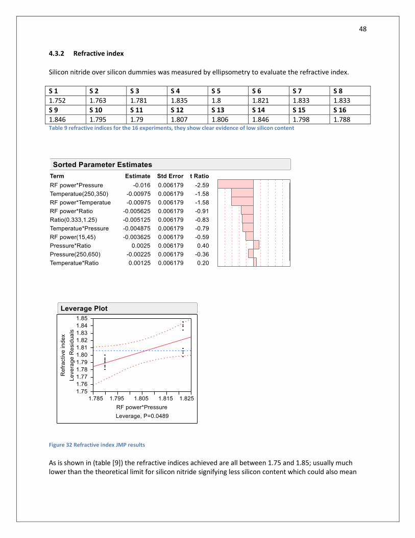
48
4.3.2 Refractive index
Silicon nitride over silicon dummies was measured by ellipsometry to evaluate the refractive index.
S 1 S 2 S 3 S 4 S 5 S 6 S 7 S 8
1.752 1.763 1.781 1.835 1.8 1.821 1.833 1.833
S 9 S 10 S 11 S 12 S 13 S 14 S 15 S 16
1.846 1.795 1.79 1.807 1.806 1.846 1.798 1.788 Table 9 refractive indices for the 16 experiments, they show clear evidence of low silicon content
Figure 32 Refractive index JMP results
As is shown in (table [9]) the refractive indices achieved are all between 1.75 and 1.85; usually much lower than the theoretical limit for silicon nitride signifying less silicon content which could also mean

49
less probability of having silicon dangling bonds and higher breakdown voltages and less Poole Frenkel currents through the dielectric.
In general the first term is the most significant on the response taking into consideration the absolute value of the t-ratio which is higher than 2. The mutual interaction between the RF power and the pressure is understandable; as in figure (22) the collision frequency scales with both the pressure (the precursor gases abundance) and the electron energy (the RF power). With the increase of both dissociative collisions are more probable to occur and more adsorbents are available in one unit of time of the deposition process. In [32] pressure was shown to increase the refractive index. This effect can be attributed also to the adsorption process itself at the surface of the specimen which is governed by Langmuir adsorption isotherms that specify that with higher pressure each layer of the deposited film has a higher coverage “the percentage of the specimen area that is covered by adsorbent species” which eventually leads to denser material and thicker layers. And the denser the film is, the higher will be its refractive index. The same applies to the RF power, which leads to the deposition of denser and more chemically and structurally homogeneous layers thus resulting in a higher refractive index [38]. Additionally with the increase of temperature hydrogen gain enough energy called “the activation energy” to desorb from the SiN, in this way the film becomes richer in Si and higher in refractive index [17] [38].

50
4.4 CV measurements
4.4.1 MIM/MIS capacitor behavior
Unambiguous stray capacitance or a defect in the measurement tool was detected when CV measurements for 5 random samples chosen from the 16 set of the DOE MIMs were taken. A step response in CV plot (fig [34])identical to the response of a Metal/ Insulator/ Semiconductor structure and a peak observed in the loss tangent curve (fig [35]) which is not intrinsic to a non leaky dielectric although the IV measurements on the same samples did not show catastrophic leakage conductance across the dielectric.
It is clear that there must be a parasitic component superimposed on the nitride CV/CF measurement. Thus since this behavior is typical to a MIS structure at accumulation and inversion regions hence there must be a MIS structure created in the vicinity of and parallel to the MIM and the channel or the depletion region would be at the interface of the SiN with the silicon substrate.
The capacitor arrangement should look like as in (fig. [33]), in this case the total capacitance would be expressed as in (equ [32]) where Wm is the depletion region width.
Figure 33
(32)
(33)
A test to prove the hypothesis made use of the 10 different areas available in the capacitors array; CV profile will be measured across different structures and compare how much will the value of the capacitance decrease after the step, the biggest percentage should be the one more affected by the MIS structure. The top electrode dimension is kept constant while the bottom contact will be changed to a

51
bigger one; this will increase the MIM area and decrease the MIS area which is dependent over the free area of the top electrode that does not overlap with the bottom electrode. The first electrode is 125 µm; the bottom was changed from 50 µm to 125 µm. Another set was measured: (c) is a structure that has a minimal overlap area between the top electrode and the semiconductor while (d) is the opposite. The effect of the silicon is much more obvious in (d).
-6 -4 -2 0 2 4
1.00E-010
2.00E-010
3.00E-010
Cp
(F
ara
ds)
U(volts)
125*125
71,8%
-6 -4 -2 0 2 4
0.00E+000
1.00E-010
2.00E-010
3.00E-010
Cp
(F
ara
ds)
U(volts)
125*50
84,5%
-6 -4 -2 0 2 4
0.00E+000
5.00E-011
1.00E-010
large top contact
Cp
(F
ara
ds)
U (volts)
90%
-6 -4 -2 0 2 4
2.80E-011
3.00E-011
3.20E-011
3.40E-011
small top contact
Cp
(F
ara
ds)
U (volts)
16%
Figure 34
1k 10k 100k
0.0
0.6
1.2
Center point
Lo
ss ta
ng
en
t
frequency (Hz)
Figure 35
a b
c d

52
By comparison of (a) with (b) and (c) with (d); the hypothesis is proven to be true. Although the formula
cannot be accurate to a great extent, because the geometry “gradient and curvature” of the electric
field distribution between the 2 contacts is more complex than assumed; however the dependency on
the 2 areas ‘A0 and AMIS’ is accounted for, and with the proportionality of both the decrease in the CV
profiled can be deduced.
A proposed solution was to coat the silicon substrate with an additional 360nm thick PECVD silicon
dioxide layer. Prior to the deposition, the tool was cleaned from any silicon nitride residuals on either
the shower head or the table; and the same cleaning process was done after finishing the SiO2
deposition prior to depositing the 16 DOE samples. The cleaning involved 2 steps as tabulated:
Step 1
Gas Pressure Temperature LF power RF power Time
CF4 150 sccm 700 mTorr 250 0C 20W pulsed pulsewidth 20s
200W continuous
8 min
Table 10
Step 2
Gas Pressure Temperature LF power RF power Time
CF4 500 sccm 500 mTorr 250 0C 50W pulsed pulsewidth 20s
100W pulsed pulsewidth 10s
8 min
Table 11
The CF4 gas that was used in the cleaning process is 80% CF4 diluted in 20% O2
For the SiO2 deposition, silane and nitrous oxide were the precursor gases, the process proceeded in a
1000mTorr pressure ambient with the table heated at 3000C for 6 minutes. The thickness was
approximately 360nm.
SiO2 RF power SiH4 N2O Pressure Temperature Time Thickness
20W 425sccm 710sccm 1000mTorr 300 0C 6 min 360nm
After the SiO2 deposition, MIM structures with SiN as dielectric were fabricated and CV measurements were done. CV plot did not show the p-type step response rather, it was a merely parabolic curve which is a natural characteristic of the silicon nitride (sect [4.6.1]) and the loss tangent proved to be constant until very high frequencies where the tool and the cable losses begin to be apparently appreciable.

53
4.4.2 Dielectric constant at 1 MHz
S 1 S 2 S 3 S 4 S 5 S 6 S 7 S 8
5.69389 3.93704 6.11943 4.73304 6.11217 4.84443 4.68554 6.20069
S 9 S 10 S 11 S 12 S 13 S 14 S 15 S 16
4.6667 5.74839 5.4863 6.36136 5.55731 5.96194 5.11567 6.27453 Table 12
Figure 36 Dielectric constant JMP results
Following the enhancement of the MIM test structure, the dielectric constant at 1 MHz was calculated from the CF plots and the data were analyzed. The dielectric constant is vital in the operation of the MISHFET as it reduces its input capacitance. The parameter that most influences the response is the power and the ratio together; this could be associated with bulk generated traps which stores charge allowing the MIM capacitor to hold more charge additional to what are placed at the metal electrodes at the same applied voltage which directly increases the structure capacitance. These traps are mainly Si dangling bonds which will occur increasingly with higher ratio ‘with the increase of silane to ammonia’ and higher RF power that increases the dissociative collision cross section of the silane. The same argument applies for the pressure that also increases the collision frequency (fig [22]).

54
4.5 IV measurements
The initial parameter in this work that we aim to optimize is the leakage currents that can be seen in IV
measurements of the MIM structures. But one problem arises when the statistical analysis is based on
the output of the IV measurements for comparison between the 16 recipes; in this case a definite
number must be withdrawn to fully represent the curve in JMP since JMP does not deal with data sets
corresponding to each recipe independently, it rather deals with one number for each sample. The only
number that could be extracted from an IV curve is the current at a specific voltage. The problem was in
the real implementation of the IV measurements; for the same sample and for the same conditions, the
curves are not reproducible. They fall in the same range but cannot be the same if accounting for margin
of error, material polarization or structural random defects …etc. So, when comparing different curves
of 16 recipes, results cannot have high credibility. It is possible –as was confirmed by measurements -
that 2 curves intersect in 2 or more points along the whole interval, which makes choosing a single point
on the IV curve at a specific voltage to compare leakage misleading. The curves are difficult to
characterize and even more they are prone to a random space of error due to the roughness of the
titanium gold contacts which cannot be neglected when having a 10 nm silicon nitride, it could alter the
near interface electric field distribution and control field emission of charge through the contact sharp
edge. The test is rather successful when dealing with a binary decision if a certain dielectric is leaky or
not. All the 16 experiments showed very good leakage suppression behavior, but it was not possible to
depend on this test to analyze the trends.
However, a second observation in the IV curves led to an additional analysis that brought more
information about the SiN behavior. A shift of the trough of the absolute value of the IV curve towards
the direction of applied bias was observed. If the sweep is from negative to positive bias, the trough will
follow to the left and vice versa. On the actual value scale, the trough corresponds to a switch in the
current polarity before the applied bias reaches zero volts; in other words, positive currents are flowing
-5 0 51E-14
1E-13
1E-12
1E-11
1E-10
1E-9
1E-8
AB
SM
IM (
A)
VMIM(V)
Figure 37 center point IV measurement of an I section 125*150 µm2 taken multiple times.

55
in the negative bias and vice versa. Additional analysis fitting the IV curves to Poole Frenkel or Fowler
Nordheim tunneling was done [35]. From the dependency equations (34) (35); PF mechanism can be
identified from a linear dependency of (J/V) on square root of (V) (fig [38] [40]), while FN mechanism can
be identified from a linear dependency of (J/V2) on the reciprocal of (V) (fig [41]).
(34)
(35)
-5 0 5
1E-13
1E-12
1E-11
1E-10
1E-9
1E-8
I(a
mp
s)
V (volts)
Figure 39 IV curves for the same sample swept from left to right and vice versa
Figure 38 PF fit plot for the red curve from -5 to 0
Figure 40 Fowler Nordheim fit plot for the red curve from –5 to 0
Figure 41 Poole Frenkel fit plot from 0 to 5 volts
0.0 0.8 1.6 2.4
-12
-10
-80.00 -0.16 -0.64 -1.44 -2.56 -4.00 -5.76
V
log
(ab
s(I
)/a
bs(V
))
sqrt(abs(V))
log(abs(I)/abs(V))
Linear Fit of log(abs(I)/abs(V))
Linear Fit of log(abs(I)/abs(V))
FN
PF
0 2 4 6 8 10
-14
-12
-10
-8
---- -1.0 -0.5-0.5 -0.3 -0.3-0.3 -0.2 -0.2-0.2 -0.1 -0.1-0.1 -0.1 -0.1-0.1
V
log
(ab
s(I
)/V
^2
)
1/abs(V)
log(abs(I)/V^2)
Linear Fit of log(abs(I)/V^2)
0.0 0.8 1.6 2.4
-10.0
-9.5
-9.0
0.000.00 0.16 0.640.64 1.44 2.562.56 4.00 5.765.76
V
log
(ab
s(I
)/V
)
sqrt(V)
log(abs(I)/V)
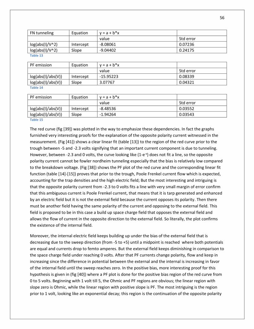
56
FN tunneling Equation y = a + b*x
value Std error log(abs(I)/V^2) Intercept -8.08061 0.07236
log(abs(I)/V^2) Slope -9.04402 0.24175 Table 13
PF emission Equation y = a + b*x
value Std error log(abs(I)/abs(V)) Intercept -15.95223 0.08339
log(abs(I)/abs(V)) Slope 3.07767 0.04321 Table 14
PF emission Equation y = a + b*x value Std error
log(abs(I)/abs(V)) Intercept -8.48536 0.03552
log(abs(I)/abs(V)) Slope -1.94264 0.03543 Table 15
The red curve (fig [39]) was plotted in the way to emphasize these dependencies. In fact the graphs
furnished very interesting proofs for the explanation of the opposite polarity current witnessed in the
measurement. (Fig [41]) shows a clear linear fit (table [13]) to the region of the red curve prior to the
trough between -5 and -2.3 volts signifying that an important current component is due to tunneling.
However, between -2.3 and 0 volts, the curve looking like (1-e-x) does not fit a line, so the opposite
polarity current cannot be fowler nordheim tunneling especially that the bias is relatively low compared
to the breakdown voltage. (Fig [38]) shows the PF plot of the red curve and the corresponding linear fit
function (table [14]-[15]) proves that prior to the trough, Poole Frenkel current flow which is expected,
accounting for the trap densities and the high electric field; But the most interesting and intriguing is
that the opposite polarity current from -2.3 to 0 volts fits a line with very small margin of error confirm
that this ambiguous current is Poole Frenkel current, that means that it is tarp generated and enhanced
by an electric field but it is not the external field because the current opposes its polarity. Then there
must be another field having the same polarity of the current and opposing to the external field. This
field is proposed to be in this case a build up space charge field that opposes the external field and
allows the flow of current in the opposite direction to the external field. So literally, the plot confirms
the existence of the internal field.
Moreover, the internal electric field keeps building up under the bias of the external field that is
decreasing due to the sweep direction (from -5 to +5) until a midpoint is reached where both potentials
are equal and currents drop to femto amperes. But the external field keeps diminishing in comparison to
the space charge field under reaching 0 volts. After that PF currents change polarity, flow and keep in
increasing since the difference in potential between the external and the internal is increasing in favor
of the internal field until the sweep reaches zero. In the positive bias, more interesting proof for this
hypothesis is given in (fig [40]) where a PF plot is done for the positive bias region of the red curve from
0 to 5 volts. Beginning with 1 volt till 5, the Ohmic and PF regions are obvious; the linear region with
slope zero is Ohmic, while the linear region with positive slope is PF. The most intriguing is the region
prior to 1 volt, looking like an exponential decay; this region is the continuation of the opposite polarity

57
PF currents “positive currents” noted in the negative bias: their maximum points coincide. This is due to
the external field -now increasing- is taking over the internal field that was enhancing the trap charge
currents and neutralizing it through pumping positive space charge. So the negative internal field is no
more negative; it is getting more and more positive and quickly diminishes and so does the current. This
decaying current “positive current” is expected then to follow traditional Ohmic conduction and finally
back to PF mechanism.
Figure 42 (a) dielectric spectroscopy from Kingery, Bowen and Uhlmann, Introduction to ceramics; (b) Poole Frenkel mechanism: electrons jump to the conduction band from the trap state and contribute to the conduction current or fall back in another trap and this is called “tap hopping”
As shown on the polarizability curve (fig [42a]), the extremely slow resonators that will charge and
discharge with a frequency nearly zero is space charge. Space charge results from mobile charges which
are present because they are impeded by interfaces, they are not discharged at an electrode or because
they are trapped in the material. Electrons or holes can be captured or localized by vacancies, interstitial
ions, impurity atoms and interface dislocations. Vacancies are the same as dangling bonds present in Si-
H and N-H radicals that act like charge traps capturing electrons to neutralize. On the other hand faster
charge build up corresponds to atomic “ionic” or electronic polarization “responsible for the refractive
index dispersion”. Bulk traps in Nitrides as mentioned before are due to Si-Si bonds acting as acceptor
traps, Si-Si antibonds acting as donor traps near the conduction bans and Silicon dangling bonds. [39]
In Frenkel Poole Conduction electrons are generally trapped in localized states. Occasionally, random
thermal fluctuations will give the electron enough energy to get out of its localized state, and move to
the conduction current. Once there, the electron can move through the material, for a brief amount of
time, before relaxing into another localized state. The Poole–Frenkel effect describes how, in a large
electric field, the electron doesn't need as much thermal energy to get into the conduction band (since
part of this energy comes from being pulled by the electric field), so it does not need a thermal
fluctuation as large and will be able to move more frequently. The current mechanism is in general
controlled by the defect states density locating just below the conduction band and above the valence
a b

58
band in the dielectric; the more there are, the nearer is the PF states either to the conduction or the
valence bands. [35]
Silicon Nitride has a marginal structural flexibility to accommodate any misplacement of the silicon and
nitrogen atoms and the density of dangling bonds is very high. In amorphous structures not all the Si
bonds are satisfied, a coordination number can be assigned to silicon and nitrogen content in the SiN to
be 3.7 and 2.78. It is frequent in deposited insulators that they would contain a high density of structural
defects. Silicon nitride (Si3N4) is an example of such material. The structural defects cause additional trap
energy states close to the band edge. These traps restrict the current flow because of a capture and
emission process, thereby becoming the dominant current mechanism with the carrier density depends
exponentially on the depth of the trap.
The build up space trapped charge under the influence of their internal electric field keep diffusing
between spatially distributed traps until reaching the bottom electrode of the device. This diffusive
motion can have relatively long relaxation time constants as denoted by our measurements. Each trap
with a single energy acts as a resonator ‘relaxation component’ when charged or discharged. They
follow the classical differential equation of Debye relaxation, when a source is applied for some time
and then it is shorted, the solution to the differential equation will be a pure exponential decay (sect
[4.6.3]). The electron emission/ trapping between the conduction band and the trapping center must
follow a response function like Debye or Cole-Cole relaxation which can be seen as the momentary delay
in the dielectric constant of a material.
These traps which are generally dangling bonds also are distributed along the bandgap of the SiN, their
electronegativity, i.e. energy is being modulated with the addition of hydrogen or oxygen atoms to the
incomplete [Si-H] or [N-H] groups whichever is dominant is depending on the radicals that could be
incorporated in the film that didn’t desorb during the deposition process; the former is a characteristic
of disilane Si2H6, aminosilane groups : mono SiH2(NH2), di and tri; while the latter corresponds to
aminosilane too SiH2(NH2)and disilamine (NH(SiH3)2. It turns out that elements with higher
electronegativity like O will drive the dangling bond trap up in the bandgap. For H, it is more
electropositive, it will increase the electropositivity if the dangling bond driving it down the band gap
These traps behave as quantum wells, where the wavefunctions or the energy states of the charge is
quantized, this quantization in a finite height potential well is affected by the bounding energies, i.e. the
electronegativities of the atoms outside the well and the physical dimension of the well. [40]
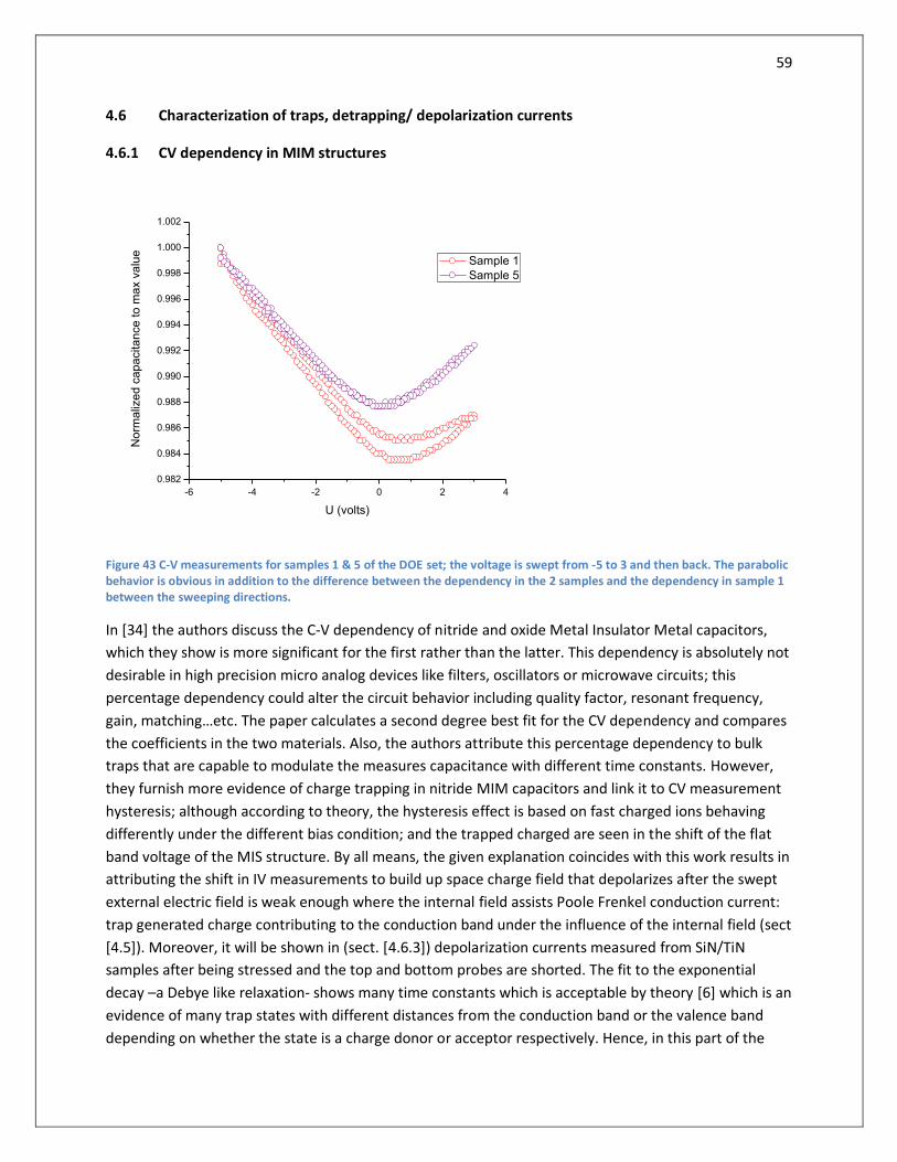
59
4.6 Characterization of traps, detrapping/ depolarization currents
4.6.1 CV dependency in MIM structures
-6 -4 -2 0 2 4
0.982
0.984
0.986
0.988
0.990
0.992
0.994
0.996
0.998
1.000
1.002
No
rma
lize
d c
ap
acita
nce
to
ma
x v
alu
e
U (volts)
Sample 1
Sample 5
Figure 43 C-V measurements for samples 1 & 5 of the DOE set; the voltage is swept from -5 to 3 and then back. The parabolic behavior is obvious in addition to the difference between the dependency in the 2 samples and the dependency in sample 1 between the sweeping directions.
In [34] the authors discuss the C-V dependency of nitride and oxide Metal Insulator Metal capacitors,
which they show is more significant for the first rather than the latter. This dependency is absolutely not
desirable in high precision micro analog devices like filters, oscillators or microwave circuits; this
percentage dependency could alter the circuit behavior including quality factor, resonant frequency,
gain, matching…etc. The paper calculates a second degree best fit for the CV dependency and compares
the coefficients in the two materials. Also, the authors attribute this percentage dependency to bulk
traps that are capable to modulate the measures capacitance with different time constants. However,
they furnish more evidence of charge trapping in nitride MIM capacitors and link it to CV measurement
hysteresis; although according to theory, the hysteresis effect is based on fast charged ions behaving
differently under the different bias condition; and the trapped charged are seen in the shift of the flat
band voltage of the MIS structure. By all means, the given explanation coincides with this work results in
attributing the shift in IV measurements to build up space charge field that depolarizes after the swept
external electric field is weak enough where the internal field assists Poole Frenkel conduction current:
trap generated charge contributing to the conduction band under the influence of the internal field (sect
[4.5]). Moreover, it will be shown in (sect. [4.6.3]) depolarization currents measured from SiN/TiN
samples after being stressed and the top and bottom probes are shorted. The fit to the exponential
decay –a Debye like relaxation- shows many time constants which is acceptable by theory [6] which is an
evidence of many trap states with different distances from the conduction band or the valence band
depending on whether the state is a charge donor or acceptor respectively. Hence, in this part of the
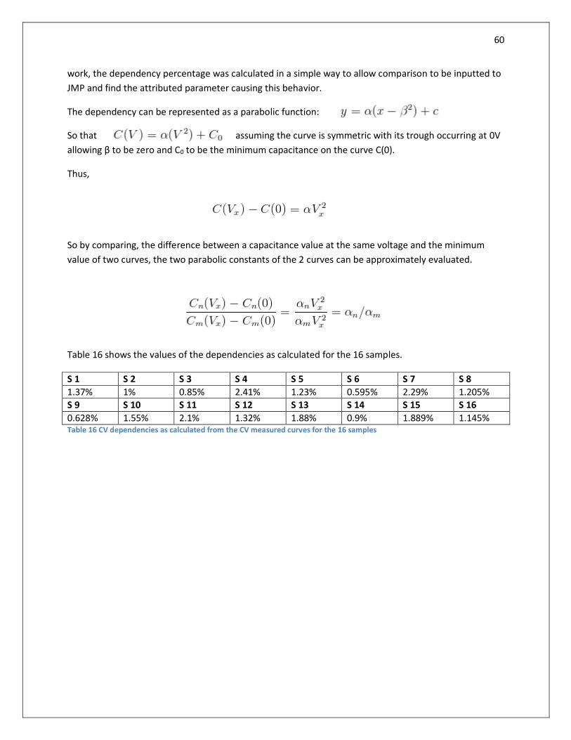
60
work, the dependency percentage was calculated in a simple way to allow comparison to be inputted to
JMP and find the attributed parameter causing this behavior.
The dependency can be represented as a parabolic function:
So that assuming the curve is symmetric with its trough occurring at 0V
allowing β to be zero and C0 to be the minimum capacitance on the curve C(0).
Thus,
So by comparing, the difference between a capacitance value at the same voltage and the minimum
value of two curves, the two parabolic constants of the 2 curves can be approximately evaluated.
Table 16 shows the values of the dependencies as calculated for the 16 samples.
S 1 S 2 S 3 S 4 S 5 S 6 S 7 S 8
1.37% 1% 0.85% 2.41% 1.23% 0.595% 2.29% 1.205% S 9 S 10 S 11 S 12 S 13 S 14 S 15 S 16
0.628% 1.55% 2.1% 1.32% 1.88% 0.9% 1.889% 1.145% Table 16 CV dependencies as calculated from the CV measured curves for the 16 samples
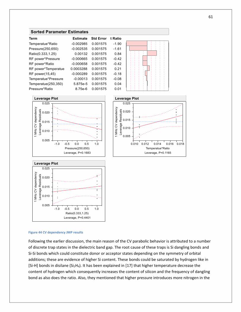
61
Figure 44 CV dependency JMP results
Following the earlier discussion, the main reason of the CV parabolic behavior is attributed to a number
of discrete trap states in the dielectric band gap. The root cause of these traps is Si dangling bonds and
Si-Si bonds which could constitute donor or acceptor states depending on the symmetry of orbital
additions; these are evidence of higher Si content. These bonds could be saturated by hydrogen like in
[Si-H] bonds in disilane (Si2H4). It has been explained in [17] that higher temperature decrease the
content of hydrogen which consequently increases the content of silicon and the frequency of dangling
bond as also does the ratio. Also, they mentioned that higher pressure introduces more nitrogen in the

62
film which by itself saturates the silicon. The sorted parameter estimate (fig. [46]) shows
“Temperature*Ratio” the most significant coefficient of the model followed by pressure. And the
leverage plots of either show that with the increase of the former, CV dependency increases and with
the decrease of the latter, CV dependency decreases. So as expected, having the temperature and ratio
increased reduces the amount of saturating hydrogen and increasing the content of silicon respectively
and increase the CV dependency; while having the pressure increased, more saturating nitrogen in
incorporated and CV dependency decreases. Note also that the ratio by itself increases the examined
response, however its corresponding t-ratio is so low for it to be considered as a significant parameter
or to have a considerable interval of confidence but still the leverage plot delivers the expected trend.
4.6.2 Stressed conduction currents
One problem in analyzing the measured IV curves is the inclusion of many current mechanisms
superimposing on each other in such a way that withdrawn conclusions from the IV curves should be
done with great care or otherwise; -sometimes- misleading or even contradictory hypotheses can be
constructed. While sweeping the MIM voltage between 2 defined values, the measured current can
include: displacement current imposed by the measuring tool probe when changing the applied
potential, conduction current (Poole Frenkel, Fowler Nordheim tunneling or hopping) and space charge
build up current or depolarization currents in the case of the change in current polarity. To eliminate
displacement, space charges build up and depolarization currents at low voltages; a stress measurement
was advised to observe only the conduction current. A constant 4 V stress voltage is applied to the MIM
structure “same area of course for the 16 recipes” for 40 seconds; thus there is no change in applied
electric field “displacement field” and after an adequate time, it is assumed that all traps are already
saturated. It will be shown in (sect [4.6.3]) that the third trap time constant in the polynomial fit is 37.7
seconds and the other time constants are smaller. Hence 40 seconds is enough for stress. This test is not
intended to identify which conduction current mechanism is involved but it quantitatively evaluates
which ones endured more currents.
S 1 S 2 S 3 S 4 S 5 S 6 S 7 S 8
2.629 54.253 8.39 1.8193 0.731665 1.2363 37.32 0.736
S 9 S 10 S 11 S 12 S 13 S 14 S 15 S 16
14.838 1.6634 39.95 0.568 3.364 0.5632 0.373 1.46 Table 17
Table [17] show the normalized stressed current in µA/mm for a structure with 104 µm2 and thickness of
approximately 10nm; each value is normalized to the thickness of its corresponding sample.

63
Figure 45
Presumably, all defective behavior in current mechanisms in the silicon nitride –including IV shift, space
charge field build up or depolarization currents- are proven to be caused by bonding defects in silicon
and their occurrence frequency. As was seen in (sect [4.4.2]) that one parameter controlling the
dielectric constant was the pressure with the ratio combined; the same argument applies in the stressed
conduction current case. For the conduction current to flow –apart from tunneling which is not
controlled by any input parameter but rather the thickness of the dielectric-, trap states must exist that
generates current under the influence of an electric field or through which carriers will hop from the
first contact interface with the dielectric to the other. Pressure when increased with ratio levels
maintained at the highest guarantee that more dissociative collisions will occur and more Silicon will be
incorporated and due to the material inflexibility to orientation; defects, dangling bonds and traps are
created. Moreover, it was stated in [38] that the pressure has another effect on the plasma chemistry
itself; the higher the pressure the shorter is the mean free path; this reduces the electron temperature
due to loss of energy with collisions; this forces the reaction to proceed incompletely and more radicals
can be incorporated with dangling bonds and structural deficiencies.

64
4.6.3 Depolarization of trapped space charge on SiN/TiN structures
Figure 46
0 20 40 60 80 100
0.00E+000
1.00E-010
2.00E-010
3.00E-010
4.00E-010
5.00E-010
6.00E-010
de
po
lari
za
tio
n c
urr
en
ts (
A)
Time (sec)
current
exponential fit
Depolarization current is the last parameter to be analyzed, to complete the qualitative evaluation of
traps and SiN deficiencies. Though it has no parameter in the JMP pool of data, it is important in proving
the existence of a build up potential -after the application of an external field- that will eventually relax
and enhances trap generated currents enhanced by an electric field. If the internal electric field does not
exist, the dipolar relaxation will be bound by random Brownian motion and an exponential decay
behavior will not be measured. For this purpose, the SiN/TiN samples were tested and connected to the
MDC mercury profiler which is in turn connected to the HP tool. A stress voltage of 4 volts for 40
seconds was applied to the specimen and then the probes were shorted and the back current into the
ground probe was measured. A depolarization current was effectively sensed by the tool. It was in the
first place a tremendously hard task to achieve this test with the MIM structures, since they are very
small and most probably the current will reside in the contact/ dielectric interface states and will not
reach the tool probe. Additionally, these very small currents cannot be sensed, stored properly by the
tool since it is a sampling tool. However, with the mercury Schottky contact to the SiN on the TiN
substrate more currents are supposed to flow since geometrically the area of the dielectric under the
electric field is many times bigger than the MIM.
(Fig [46]) shows the curves of the SiN/TiN depolarization with the fit, on the left is one sample, the red
curve is the fit curve on top of the original black curve and on the right is the depolarization curves of
many samples. The time constants T1, T2, T3 of the fit are 2.98, 9.66 and 37.7 seconds respectively
different trap time constants, so different resonance frequencies (like the trap states’ peaks in the
conductance method). This definitely proves the existence of different trap energies, which was
explained before with the near atoms bonding modulating the electronegativity of the dangling bonds
[40] and proves the existence of the relaxing internal electric field established after the stress leading to
the same evidence of the occurrence of traps. These were shown before to be mainly cause by high
pressure and high ratio.
0 20 40 60 80 100 120
-6.50E-010
-6.00E-010
-5.50E-010
-5.00E-010
-4.50E-010
-4.00E-010
-3.50E-010
-3.00E-010
-2.50E-010
-2.00E-010
-1.50E-010
-1.00E-010
-5.00E-011
0.00E+000
5.00E-011
IMIM
(A)
Time (S)

65
Equation Y=A1exp(-x/τ1)+ A2exp(-x/τ2)+ A3exp(-x/τ3)+y0
Value Standard Error Y0 1.79133E-11 7.62622E-13
A 2.11581E-10 7.34104E-12
τ1 2.98497 0.06217
A2 1.86402E-10 3.82353E-12 τ 2 9.66254 0.4815
A3 1.02955E-10 5.69141E-12
τ 3 37.72077 2.0585 Table 18 The fit to the exponential decay in fig (46) with the different time constants and the standard error
To describe this behavior qualitatively, the displacement field of a material is connected to its polarization that induces the causality in the material response to an external applied electric field; that is it cannot polarize instantaneously in response to the field. (Equ [])
(36)
(37) (38)
The polarization is not a linear function but it is depending on the field frequency, this is where the dielectric spectroscopy or dispersion arises (equ [37]). The polarization can be expressed as a convolution of the electric field at previous times with time-dependent susceptibility given by χe(Δt) multiplied by ε0 ‘dielectric permittivity of free space’.
If then the current can be expressed as the sum of conduction current and displacement current (36) then it will be as in (equ [39]) by substituting (equ [38]) into (equ [36])
(39)
(40)

66
(Equ [39]) presents all current mechanism that can be present in a dielectric; if multiplied by the
capacitor area A and divided by free space permittivity and capacitor thickness d; all accounting for a
constant C0; then we get a simpler equation (40) relating voltage and current.
A test could then be made with the application of a constant current –where there is no time change
amounting for null time derivative- we can find the polarization function χe(t) given that we know what
is the conductivity of the material (equ [41]). However, if the field is shorted, there will be no conduction
current component and the depolarization function in this case can be computed -χe(t) and it is exactly
the same as the polarization function; only the signs change (equ [42])
(40)
(41)
The exponential profile in (fig [46]) is the depolarization function. It is the solution of the current
continuity equation (equ [42]) when taking into consideration multiple current trap states or time
constants and the conductivity is zero; that’s when the applied field is shorted and only the dielectric
material is allowed to relax (equ [43]).
(42)
(43)

67
5. Recent MISHFET results & current work
Recent MISHFETs have been processed with dielectrics tabulated in (table [19]), they showed more than
2 orders of magnitude of gate leakage suppression (fig [47]) and high breakdown field (fig [50]). The
MISHFETs showed the same trough shift and opposite current polarity in the negative bias and in the
positive bias. The behavior is symmetric (fig [49]) when the gate is swept over a smaller range of voltage
from -4 to 4 volts. The devices are currently subject to more analysis.
Sample RF power Temperature Pressure Ratio SiH4/NH3 Time Thickness
X2 45 350 650 1.25 36/29sccm 1:35 8.06nm
X4 45 350 250 0.333 17/50sccm 4:10 9.54nm
Y2 15 350 250 0.333 17/50sccm 5:10 9.45nm Y4 15 250 650 0.333 17/50sccm 4:10 9.96nm Table 19
-20 -15 -10 -5 0 5
1E-11
1E-10
1E-9
1E-8
1E-7
1E-6
1E-5
1E-4
1E-3
0.01
0.1
1
10
100
1000
10000
no
rma
lize
d c
urr
en
t [A
/cm
^2
]
voltage
X2
X3
Y2
Y4
X4
-22 -20 -18 -16 -14 -12 -10 -8 -6 -4 -2 0 2 4 6
1E-11
1E-10
1E-9
1E-8
1E-7
1E-6
1E-5
1E-4
1E-3
0.01
0.1
1
no
rma
lize
d c
urr
en
t (A
/cm
^2
)
voltage
X3
Y2
Y4
-4 -2 0 2 4
1E-10
1E-9
1E-8
1E-7
no
rma
lize
d c
urr
en
t (A
/cm
^2
)
voltage
Y4
Figure 47 Figure 48
Figure 49
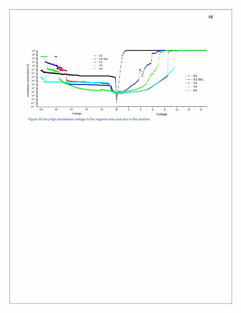
68
Figure 50 very high breakdown voltage in the negative bias and also in the positive
0 2 4 6 8 10 12 14
X2
X3 Std.
Y2
Y4
X4
Voltage
-100 -80 -60 -40 -20 0
10-11
10-10
10-9
10-8
10-7
10-6
10-5
10-4
10-3
10-2
10-1
100
101
102
103
104
X2
X3 Std.
Y2
Y4
X4
no
rma
lized
curr
en
t [A
/cm
^2]
Voltage

69
7. References
[1] “Semiconductor material and device characterization”, Dieter K. Shroeder, Jan 2006
[2] Plasma mathematical calculation is a courtesy of Prof. Darek Korzec, German University in Cairo;
from his lectures on semiconductor technology, 2008
[3] “Glow discharge processes: Sputtering and plasma etching”, Brian Chapman, Sep 1980
[4] “Plasma electronics” applications in microelectronic device fabrication by T Makabe and Z
petrovic.
[5] “Introduction to plasma physics”, Robert J Goldstone and Paul H Rutherford, plasma physics
laboratory, Princeton University
[6] “Introduction to ceramics”, 2nd Edition by W. David Kingery, H. K. Bowen, and Donald R.
Uhlmann, 1976.
[7] “Handbook of chemical vapor deposition, principles, technology and applications”, second
edition, Hugh O. Pierson
[8] “Leakage in Nanometer CMOS technologies“ by Siva G. Narenda and Anantha Chandrakasan
[9] “Gallium nitride based microwave high power heterostructure field effect transistors, design
and technology and characterization” PhD dissertation 2006 by M.C.J.M.C. Kraemer
[10]“Nitride semiconductor devices” by Joachim Piprek 2007
[11] “Spontaneous and piezoelectric polarization in nitride semiconductors” Edward T. Yu, Book
chapter for inclusion in III-V nitride semiconductors: Applications and devices by E.T.Yu and
O.Manasreh.
[12] E.H. Nicollian and A. Goetzberger “The Si-SiOx interface – electrical properties as determined by
the metal-insulator-silicon conductance technique” The Bell system technical journal July –
August 1967
[13] S.K.Streiffer, “Relaxation currents” presentation Argonne national laboratory (2000)

70
[14]William E. Courtney, “Analysis and evaluation of a method of measuring the complex
permittivity and permeability of microwave insulators”, IEEE transactions on microwave theory
and techniques, VOL. MIT-18, No. 8, August 1970
[15]T.P. Ma, “electrical characterization of high-k gate dielectrics”
[16]K.R. Lee, D.C. Malocha, and K.B. Sundaram, “Investigation of PECVD silicon nitride films for
surface wave devices”, 1992 IEEE ultrasonics symposium proceedings, pp 369-371.
[17]S. Ponce-Alcantra, C. Del Canizo, J. Hofstetter, and A. Luque “the effect of RF and MW power on
the SiNx films grown by PECVD”, IEEE transactions on plasma physics (2007)
[18]Byungwham Kim and Wan-Shick Hong, “use of neural network to characterize a low pressure
temperature effect on refractive property of silicon nitride film deposited by PECVD”, IEEE
transactions on plasma science, vol. 32, No. 1, February 2004
[19]Byungwham Kim, Seung-Soo Han, Tae Seon Kim, Bum Soo Kim and Il Joo Shim, “Modeling
refraction characteristics of silicon deposited in a SiH4-NH3-N2 plasma using neural network”
IEEE transactions on plasma science, vol. 31, No. 3, June 2003
[20]Mashiko Maeda, Ei-ichi Yamamoto, Shin-ichi Ohfuji, Manabu Itsumi, “dielectric characteristics of
a metal-insulator-metal capacitor using plasma enhanced chemical vapor deposited silicon
nitride films” Journal of vacuum science technology Jan/Feb 1999
[21]M. Eickelkamp, D. Fahle, J. Lindner, M. Heuken, C. Lautensack, A. Noculak, H. Kalisch, R.H. Jansen
and A. Vescan, “Systematic investigation of the influence of gate insulator thickness on the
electrical performance of Al2O3-based AlGaN/GaN MISHFETs on Si(111) substrates” WOCSDICE
proceedings May 2009
[22]S. Saygi, A. Koudymov, V. Adivarahan, J. Yang, G. Simin, M. Asif Khan, J. Deng, R. Gaska, M.S.
Shur, “Real space electron transfer in III nitride metal oxide semiconductor heterojunction
structures” applied physics letters, 87, 043505 (2005)
71
[23]Masaru Ochiai, Mitsutoshi Akita, Yutaka Ohno, Shigero Kishimoto, Kouichi Maezawa and Takashi
Mizutani, “AlGaN/ GaN Heterostructure metal insulator semiconductor high electron mobility
transistor with Si3N4 gate insulator” Japanese Journal of applied physics Vol. 42(2003) pp.2278-
2280
[24]Michel Marso, Gero Heidelberger, Klaus Michael Indlekofer, Juraj Bernat, Alfred Fox, P. Kordos
and Hans Lueth, “Origin of improved RF performance of AlGaN/GaN MOSHFETs compared to
HFETs” IEEE transactions on electron devices, Vol. 53, pp/ 1517-1523, July 2006
[25]M. A. Khan, G. Simin, J. W. Yang, J. P. Zhang, A. Koudymov, M. S. Shur, R. Gaska, X. H. Hu, and A.
Tarakji, “Insulating gate III-N heterostructure field effect transistors for high power microwave
and switching applications” IEEE Transactions on microwave Theory and Techniques, vol.51, pp.
624-633, 2003.
[26]D. Gregusova, R. Stoklas, K. Cico, T. Lalinsky, and P. Kordos, “AlGaN/GaN metal oxide
semiconductor field effect transistors with 4 nm thick Al2O3 gate oxide ” Semiconductor Science
and Technology, vol.22, pp. 947-951, 2007.
[27]R. N. Wang, Y. Cai, C. W. Tang, K. M. Lau, and K. J. Chen, “Enhancement-mode Si3N4 / AlGaN /
GaN MISHFETs,” IEEE Electron Device Letter, vol. 27, pp. 793-795, 2006
[28]C. Liu, E.F. Chor, and L.S. Tan, “Enhancement device performance of AlGaN/GaN HEMTs using
HfO2 high- k dielectric for surface passivation and gate oxide” Semiconductor Science and
Technology, vol. 22, pp.522-527 , 2007.
[29]Minseok Jo, Hokyung Park, Man Chang, Hyung-Suk Jung, Jong-Ho Lee, and Hyunsang Hwang,
“Oxygen vacancy induced charge trapping and positive bias temperature instability in HfO2 n-
MOSFET” Science direct, Electronic Engineering vol. 84 pp.1934-1937(2007)

72
[30]Kjell Nybergh, Teemu Marjamaki and Eija Skarp, “Modeling the growth of PECVD silicon nitride
films for crystalline silicon solar cells using factorial design and response surface methodology”
26th photovoltaic specialists conference; September 30-October 3, 1997; Anaheim, California.
[31]J.P. Manceau, S. Bruyere, S. Jeannot, A. Sylvestre and P. Gonon, “Leakage current variation with
time in Ta2O5 MIM and MIS capacitors” 2006 IEEE IIRW final report
[32]Hamood Ur Rahman, Angus Gentle, Eric Gauja, Rodica Ramer, “Characterization and
optimization of PECVD silicon nitride as dielectric layer for RF MEMS using reflectance
measurements” 2008 IEEE processings
[33]Chih-Cheng Lu, Chong Long Hu, Meng-chyi Wu, Tian Tsrong Shi and Wen-Jeng Ho, “Electrical
Characterization of SiOx and SiNx prepared by PECVD technique on In0.53Ga0.47As” IEEE
transactions on Dielectrics and electrical insulations, Vol. 8 No.6, December 2001
[34]Jeffrey A. Babcock, Scott G. Balster, Angelo Pinto, Christoph Dirnecker, Philipp Steinmann,
Reiner Jumpertz and Badih El Kareh, “Analog characterization of metal insulator metal
capacitors using PECVD nitride dilectrics” IEEE electron device letters, Vol. 22, No. 5, May 2001
[35]Hidefumi Sato, Hiromitsu Kato, Yoshimichi Ohki, Kwang Soo Seol and Takashi Noma, “Electrical
properties in silicon oxynitride and silicon nitride prepared by Plasma enhanced chemical vapor
deposition” IEEE
[36]T.K. Saha and P. Purkait, “Investigation of polarization and depolarization current measurements
for the assessment of oil-paper insulation of aged transformers” IEEE transactions on dielectrics
and electrical insulation, Vol. 11, No.1; February 2004
[37]David J. Collins, Andrzej J. Strojwas and Daniel D. White, Jr., “A CFD model for the PECVD of
silicon nitride” IEEE transactions on semiconductor manufacturing, Vol. 7, No. 2; May 1994

73
[38]Seung-Soo Han, Li Cai, Gary S. May and Ajeet Rohatgi, “Modeling the growth of PECVD silicon
nitride films for solar cell applications using neural networks” IEEE transactions on
semiconductor manufacturing, Vol. 9, No. 3, August 1996
[39]Meng Tao, Daegyu Park, S. Noor Mohammad, Ding Li, Andrei E. Botchkerav and Hadis Morkoc,
“Electrical conduction in silicon nitrides deposited by plasma enhanced chemical vapor
deposition” Philosophical magazine B, 1996, Vol. 73, No. 4, 723-736
[40]G. Lucovsky and S.Y. Lin, “Near neighbor chemical bonding effects on Si atom native bonding
defects in silicon nitride and silicon dioxide insulators” Journal of Vacuum science technology.
Jul/Aug 1985
[41] Martin Eickelkamp “Herstellung und Characteriseirung von AlGaN/GaN HFETs, Einfluss der
Epitaxie und Prozessierung auf die elektrischen Eigenschaften” Diplomarbeit RWTH-Aachen
(2006)
[42] E. Alekseev and D. Pavlidis “DC and high frequency performance of AlGaN/GaN heterojunciton
bipolar transistors” Solid State Electronics, Vol. 44, 245-252 (2000)
[43] O. Ambacher, J. Smart, J. R. Shealy, N. G. Weimann, K. Chu, M. Murphy, W. J. Schaff, L. F.
Eastman, R. Dimitrov, L. Wittmer, M. Stutzmann, W. Rieger and J. Hilsenbeck “Two dimensional
electron gases induced by spontaneous and piezoelectric polarization charges in N- and Ga- face
AlGaN/GaN heterostructures” Journal of Applied Physics, Vol. 85, No. 6, 3222-3233 (1999)
[44] Isamu Akasaki and Hiroshi Amano "Crystal Growth and Conductivity Control of Group III Nitride
Semiconductors and Their Application to Short Wavelength Light Emitters". Japanese Journal of
Applied Physics 36: 5393–5408 (1997)
[45] Shinji Terao, Motoaki Iwaya, Ryo Nakamura, Satoshi Kamiyama, Hiroshi Amano and Isamu
Akasaki "Fracture of AlxGa1-xN/GaN Heterostructure —Compositional and Impurity
Dependence". Japanese Journal of Applied Physics 40: L195-L197 (2001)

74
[46]H. Amano et al. “Metalorganic vapor phase epitaxial growth of a high quality GaN film using an
AlN buffer layer”. Applied Physics Letters 48: 353 (1986)
[47] Asif Khan, M. "Metal semiconductor field effect transistor based on single crystal GaN". Applied
Physics Letters 62: 1786 (1993)
[48] JMP 5.1.2 DOE guide, JMP, SAS campus drive, Cary, North Carolina 27513
[49] Statistics / DOE intro by Jason McCormick
[50]“DoE Design of Experiments Einführung in die Statistische Versuchplannung” by Beat Giger TQU
AG, Winterthur
[51]Masayuki Kuroda, Tomohiro Murata, Satoshi Nakazawa, Toshiyuki Takizawa, Masaaki Nishijima,
Manabu Yanagihara, Tetsuzo Ueda and Tsuyoshi Tanaka “High Fmax with high break down
voltage in AlGaN/GaN MIS-HFETs using in-situ SiN as gate insulators” IEEE 2008

75
8. Appendix [A]
GENERAL CHARACTERISTICS OF NITRIDES6 They are hard and wear-resistant and have high melting points and good chemical resistance. Most are important industrial materials and have a number of major applications in cutting and grinding tools, wear surfaces, semiconductors, and others. Their development is proceeding at a rapid pace and CVD is a major factor in their growth. [1] Refractory-Metal (Interstitial) Nitrides Interstitial nitrides are crystalline compounds of a host metal and nitrogen, where the nitrogen atom occupies specific interstitial sites in the metal structure. The interstitial nitrides have several important characteristics. • They have a complex electronic bonding system, which includes metallic, covalent, and ionic components. • They are primarily non-stoichiometric phases. • They have high hardness and strength. • Like metals, they have high thermal and electrical conductivity. • Like the carbides, they allow nonmetal vacancies (i.e., nitrogen) in the lattice. • Unlike the carbides, they tolerate metal-atom vacancies. Moreover, the interstitial nitrides are susceptible to the presence of even minute amounts of impurities such as hydrogen and particularly oxygen which tend to distort the structure. To avoid such harmful contamination, it is necessary to maintain a deposition system that is completely free of oxygen and hydrogen. *This is not the type of the compound we’re developing. [2] Covalent Nitrides The atomic and crystalline structure of the three covalent nitrides, aluminum, boron, and silicon nitrides, is less complex than that of the interstitial nitrides. Their bonding is essentially covalent, that is, the nitrogen atoms bond to the aluminum, boron, or silicon atoms by sharing pairs of electrons and, like all covalent bonds, these atoms form definite bond angles. The bonding is achieved by the hybridization of the valence electrons of the respective atoms. The three covalent nitrides have the following common features • They have high melting point and thermal and chemical stability. • All three have similar cubic structures (although boron nitride also has a graphite-like structure). • They have low density and low atomic weight. • They are good electrical insulators. • They are hard and strong materials and exhibit typical ceramic characteristics. • All three are produced industrially by CVD with important applications.
6 “Handbook of chemical vapor deposition, principles, technology and applications”, second
edition, Hugh O. Pierson

76
[3] Material properties
Molecular Weight: 140.28 g/mol Color: colorless if pure. Having very low thicknesses exhibits light diffraction with a wavelength corresponding to the thickness. Theoretical Density (g/cm3): 3.187 (β), 3.184 (α) Melting Point: 1900 C Specific Heat (J/g.K): 0.54 to 0.7 in another form (J/mole.K): 75.7 to 98.2 Thermal Conductivity: 25–36 W/m.C Thermal Expansion (10-6/ Celsius): 2.8 to 3.2 over the range of 0 to 100 Celsius Electrical Resistivity: 1014 Ω .cm Dielectric Constant @35 GHz: 7.9 to 8.14 Loss Tangent @35 GHz: 0.0017–0.0006 Vickers Hardness: 16 to 18 GPa Weibull Modulus: 15 to 30 MPa Fracture Toughness 5 to 7.5 MPa Young’s Modulus: 260 to 330 GPa Poisson’s Ratio: 0.23 to 0.27 Flexural Strength: 600 to 1200 MPa In those data the test temperature is 20C otherwise specified [4] Applications The market for silicon nitride is fast growing, particularly in structural and chemical resistance applications and as a thin film in semiconductor devices. • Crucibles for silicon single-crystal processing. • Crucibles and vessels for handling corrosive chemicals and molten metals. • High-temperature gas-turbine components. • Diesel-engine components. • Rotors for turbocharger. • Cutting tools (Si3N4 and Sialon ceramics). • Components for welding, tube drawing, and extruders. • Ball and roller bearings. • Bearing seals and check valves. • Blast nozzles. • Thermocouple tubes. • Heat exchangers, pumps, and seal faces. • Passivation layers, multilayer resist stacks, diffusion barriers, interlevel dielectrics, side-wall spacers, trench masks, oxidation masks, etc., in semiconductor devices. • Whiskers for high strength reinforcement.