gan substrates for iii-nitride devices - diva portal
TRANSCRIPT
Linköping University Post Print
GaN Substrates for III-Nitride Devices
Tanya Paskova, Drew A. Hanser and Keith R. Evans
N.B.: When citing this work, cite the original article.
©2009 IEEE. Personal use of this material is permitted. However, permission to
reprint/republish this material for advertising or promotional purposes or for creating new
collective works for resale or redistribution to servers or lists, or to reuse any copyrighted
component of this work in other works must be obtained from the IEEE.
Tanya Paskova, Drew A. Hanser and Keith R. Evans, GaN Substrates for III-Nitride Devices,
2010, Proceedings of the IEEE, (98), 7, 1324-1338.
http://dx.doi.org/10.1109/JPROC.2009.2030699
Postprint available at: Linköping University Electronic Press
http://urn.kb.se/resolve?urn=urn:nbn:se:liu:diva-58340

CONTRIBUTEDP A P E R
GaN Substrates forIII-Nitride DevicesBulk gallium nitride substrates for optoelectronic devices have been under
intense development, and availability of this crystalline material has
been increasing in size, doping, and orientation.
By Tanya Paskova, Drew A. Hanser, and Keith R. Evans
ABSTRACT | Despite the rapid commercialization of III-nitride
semiconductor devices for applications in visible and ultra-
violet optoelectronics and in high-power and high-frequency
electronics, their full potential is limited by two primary
obstacles: i) a high defect density and biaxial strain due to
the heteroepitaxial growth on foreign substrates, which result
in lower performance and shortened device lifetime, and
ii) a strong built-in electric field due to spontaneous and
piezoelectric polarization in the wurtzite structures along the
well-established [0001] growth direction for nitrides. Recent
advances in the research, development, and commercial
production of native GaN substrates with low defect density
and high structural and optical quality have opened opportu-
nities to overcome both of these obstacles and have led to
significant progress in the development of several opto-
electronic and high-power devices. In this paper, the recent
achievements in bulk GaN growth development using different
approaches are reviewed; comparison of the bulk materials
grown in different directions is made; and the current
achievements in device performance utilizing native GaN sub-
strate material are summarized.
KEYWORDS | Ammonothermal growth; doping; gallium nitride
(GaN); heterostructure field-effect transistor (HFET); hydride
vapor phase epitaxy; laser diode (LD); light-emitting diode
(LED); native substrates; point defects; Schottky diodes; solu-
tion growth; structural defects; surface orientation; thermal
conductivity
I . INTRODUCTION
Nitride-based devices such as ultraviolet (UV)-blue-green
emitters, high-power transistors, detectors, etc., have
became commercial realities relying completely on het-
eroepitaxial approaches by employing a variety of foreign
substrates including, sapphire, silicon carbide, and silicon.
However, their performance is significantly limited by the
structural quality of these materials as a result of the well-
known disadvantages of the heteroepitaxy, such as latticemismatch, thermal expansion coefficient mismatch and
chemical incompatibility leading to high-dislocation den-
sity, mosaic crystal structure, biaxial induced stress, and
wafer bowing. In order to reduce these structural defects,
special approaches have been developed such as low-
temperature buffer technologies or epitaxial lateral over-
growth (ELOG) techniques, which complicate and extend
the device growth process. Additional drawbacks arerelated to the lower electrical and/or thermal conductivity
of most foreign substrates, which require more compli-
cated and expensive device designs.
Availability of lattice matched GaN substrates can bring
not only a new quality in GaN-based devices by improved
device performance through eliminating the structural
defects and providing better vertical electrical and thermal
conductivity; moreover, it will lead to cost-efficient deviceprocessing through simplification of the epitaxial growth
process by eliminating the need for low-temperature buffer
layers. In this paper, we summarize the major efforts in
GaN substrate development and present the current
achievements in producing large-scale high-quality native
GaN substrates with different surface orientations. We
discuss the advantages of using the native GaN substrates
with respect to the current heteroepitaxial nitride-baseddevices. Some specific devices with improved performance
are described before a short summary is given.
II . MAJOR EFFORTS IN GaNSUBSTRATE GROWTH
In contrast to classical semiconductors like silicon and
gallium arsenide, for which the development of substrates
and thin-film device structure went hand-by-hand, the
Manuscript received April 8, 2009; revised June 26, 2009; accepted August 4, 2009.
Date of publication November 24, 2009; date of current version June 18, 2010.
The authors are with Kyma Technologies, Inc., Raleigh, NC 27617 USA
(e-mail: [email protected]; [email protected]; [email protected]).
Digital Object Identifier: 10.1109/JPROC.2009.2030699
1324 Proceedings of the IEEE | Vol. 98, No. 7, July 2010 0018-9219/$26.00 �2010 IEEE

III-nitride thin-film device technology is by far advancedover the development of native substrate crystal growth.
However, recently there has been considerable interest
and widespread ongoing research and development efforts
to change this situation. Several methods, considered with
high potential to deliver high quality and/or cost-effective
and scalable native GaN crystals, are currently under
intensive development. In this paper, however, we only
focus on the techniques that demonstrated ability to pro-duce relatively large bulk crystals, in shape of boules with
diameter of 2 in and thickness up to several millimeters,
which allow producing of substrates with different surface
orientations.
A. Hydride Vapor Phase EpitaxyCurrently, hydride vapor phase epitaxy (HVPE) is
considered to be a highly practical method to obtain GaNthick layers that can serve as quasi-bulk substrates after
delaminating from the foreign substrates or to obtain GaN
boules that can be sliced to fabricate native bulk substrates.
The biggest advantage of the technique is its ability to
produce high-quality material at high growth rates due to a
high surface migration of the halide species, motivating the
versatility of HVPE as a growth method for both device
applications and substrate application. Among all the bulkgrowth techniques under investigation today for nitrides,
HVPE is the most promising technique since it utilizes a
process at more favorable conditions, namely, low pressure
and relatively low growth temperature. Combined with the
high growth rate, it determines the growth process to be
also cost effective.
Nowadays, the fundamental growth physics and chem-
istry of HVPE growth of GaN are well understood. Theavailable models [1], [2] of the kinetics of the process and
growth mechanisms occurring at the solid/vapor interface
during HVPE growth of GaN assume a surface process
involving several steps and allow simulation of the growth
rates. Based on a quasi-thermodynamic growth model,
simulations of gas dynamics, temperature distribution, and
partial pressures can be simulated for any specific reactor
design [3], [4]. Commonly the HVPE process for growingIII-nitrides consists of two main reactions: i) forming chlo-
ride gas of the group III metal at relatively lower growth
temperature and ii) growth reaction between the chloride
metal and ammonia to form the nitride film at higher
growth temperature, typically in the range of 1050 �C–
1100 �C. Basically, two temperature zone reactors are
needed in horizontal or vertical design, but often more
temperature zone reactors are employed with a higherflexibility for temperature control and particularly in case
of doping varieties.
The HVPE technique was proven capable to produce
n-type, p-type, and semi-insulating material. The HVPE-
GaN material always exhibits unintentional n-type con-
ductivity, related to background doping by silicon and
oxygen, introduced from the quartz parts within the
reactor and/or from the process gases. For intentionaln-type doping, silicon and oxygen are mostly used, but
doping by Ge and Sn has also been explored. The Si doping
can be achieved either by introducing gas [5], silane ðSiH4Þ,disilane ðSi2H6Þ, or dichlorsilane ðSiH2Cl2Þ or by exposing
solid Si to HCl to form SiClx [6]. The latter was reported to
ensure the highest intentional free carrier concentration
of 8� 1018 cm�3 [6]. The p-type doping in HVPE GaN
growth can be achieved by using Zn [7], Cd [8], Be [9], orMg [10], [11]. Today Mg doping, shown to be relatively
more efficient, is mostly used by adding pure metal or
powder Mg in a separate boat or mixed with Ga metal and
exposed to the HCl. The use of H2 carrier gas and its effect
on the efficacy of p-type doping with Mg is a point of
controversy in the reports due to the formation of Mg-H
complexes and the need for thermal annealing that is
usually performed in situ directly after the growth. Thesemi-insulating type of HVPE-GaN was reported by using
Fe compensating doping [12], [13], achieving free carrier
concentration as low as 5� 1013 cm�3 [13].
The optimization of the HVPE-GaN growth is impeded
by the typical complications of crystal growth technology
like the multidisciplinary nature and complex multiparam-
eter character of the process. In addition, the nucleation
optimization was of significant importance. Several tech-niques resulted in significant improvements, such as dif-
ferent single buffers of ZnO [14], [15], metal-organic
chemical vapor deposition (MOCVD) grown GaN thin
layers [16], [17], reactively sputtered AlN [16], [18], or TiN
[19], and also different modifications of growth forced in
lateral in-plane directions, as ELOG around masks of dif-
ferent materials and shapes [20]–[22] or grooved substrates.
The selection of the nucleation scheme determines the typeof HVPE GaN layers usually produced with different
thicknesses and different characteristics.
B. Ammonothermal GrowthThe ammonothermal process is a solvothermal process
that allows the solubilization of polycrystalline III-nitride
nutrient or feedstock in supercritical ammonia under high
pressure by utilizing a solubilizing agent or mineralizer. Thedissolved nutrient is then transported to the region of
crystallization, where it recrystallizes on seed crystals or
through self-seeding. The type of the mineralizer used
determines the main type of the ammonothermal approach,
with respective advantages and disadvantages. The minera-
lizers are generally divided into three groups: i) basic
mineralizer, which introduces NH�2 ions to the solution;
ii) acidic, which introduces NHþ4 ions; and iii) neutral,which does not introduce either of them. Dissolution of
III-nitrides using potassium azide ðKN3Þ or potassium
amide ðKNH2Þ ammonothermal-basic solutions [23]–[26]
has been suggested by several groups to occur through
formation of soluble intermediate compounds, which sub-
sequently decompose with temperature. Other crystalliza-
tion mechanisms, which involve forward solubility of
Paskova et al. : GaN Substrates for III-Nitride Devices
Vol. 98, No. 7, July 2010 | Proceedings of the IEEE 1325

nitride species, have been reported for ammonothermal-acidic [27]–[29] solutions, which utilize ammonium halide
mineralizers. The ammonothermal-basic growth is con-
ducted by transporting the mass from high- to low-
temperature zones and has been reported to possess several
advantages, including lower dissolution density due to
solubilizing in the higher temperature zone; lower contam-
ination probability due to recrystallization in the lower
temperature zone; lower probability for cubic formation;and absence of disastrous effect of the basic solution on the
autoclave materials, which results in safety improvements
and cost effectiveness. In contrast, the acidic approach
requires special, usually costly, Au or Pt liners, and still the
safety operation remains problematic. Nevertheless, the
approach is expected to be capable of handling higher
growth rates at higher pressures [29].
In general, the ammonothermal technique is charac-terized with relatively low growth rate capacity; however,
it requires relatively low temperature and reasonable
pressure, which allow controllable recrystallization at
close to equilibrium conditions, which in turn allows
production of high-quality material. In addition, the
technique allows large-scale wafer growth and scalable
production approach by conducting multiple seeded
growths in a single run.The quality of this type of material is still in the begin-
ning of detailed evaluation. Given the fact that a rea-
sonable large cystal is a result of a very long process,
optimization of the growth conditions and producing a
systematic series for thorough analysis will take more time.
Nevertheless, the first experimental results indicate that
the properties of the ammonothermal GaN material are
very strongly influenced by the quality and surface prepa-ration of the seeds used. The best results from the crys-
tallinity point of view were reported for self-prepared seed
and multiple regrowth processes [30]. Dislocation presence
was not revealed by standard etch pit density and catho-
doluminescence techniques, and the curvature of samples
with diameter up to 2 in has been measured to be more
than 1000 m. The free carrier concentration of undoped
samples was reported to be usually in the range of 1019 cm�3
[24]–[26] but can go down to 2� 1018 cm�3 [30].
C. Solution Growth at Lower Pressure,Lower Temperatures
An alternative solution growth approach by using Na
flux instead of nitrogen solution was proposed by
Yamane et al. [31] several years ago. The advantages of
this approach are mostly related to the more favorablegrowth conditions of typically 800 �C and 5 MPa. The
results for self-nucleation growth so far are quite similar to
that obtained by high-pressure solution growth approach.
In the absence of a GaN seed, two growth habits were
demonstratedVprisms or plateletsVwith length and
lateral sizes of a few millimeters. Kawamura et al. [32]
have modified the Na-flax method for growth on 2-in
templates. In the case of using GaN film grown byMOCVD, growth rates up to 20 �m/h were attained, and a
boule with a thickness of 3 mm was shown. Another ad-
vantage of this liquid epitaxial method is its ability to re-
duce some structural defect density, consistent with
reports for other material systems such as SiC. A decrease
of dislocation density from 108 cm�2 in the seed to
104 cm�2 in the regrown material was reported and
explained in terms of a change in the dominating growthmode from vertical in the seed to lateral in the Na-flux
solution growth [33].
Similar results of reducing the dislocation density have
been reported for alternative low-pressure solution
growth (LPSG) at growth temperature in the range of
900 �C–1020 �C [34] by employing a different chemical
solution. A growth rate of 1 �m/h was reported for growth
on metalorganic vapor phase epitaxy (MOVPE) GaN tem-plated sapphire up to 3-in in diameter. Also, at nearly
atmospheric pressure and temperature of about 800 �C,
employing another chemical solvent, seeded growth on an
HVPE-GaN seed was demonstrated [35]. Up to now, the
reported growth rates of a few micrometers per hour are
not suited for bulk crystal growth. In addition, since in
these approaches nitrogen has to be dissolved and then
diffused through the Ga melt to the growth front, main-taining homogeneous growth over large areas remains a
challenge.
A short comparative summary of the current achieve-
ments in producing largest GaN crystals by the three
techniques is shown in Table 1.
III . CURRENT ACHIEVEMENTS IN GaNSUBSTRATE DEVELOPMENT
Since HVPE is the method that dominates the GaN
substrate market today, we will focus further in this paper
on the different approaches used by this technique only.
The specific characteristics of the material available on the
market are not included in this paper. There are several
thorough reviews in the literature [36]–[43] discussing the
properties of the HVPE grown GaN in detail, which werecommend to interested readers. It is important to note
that the growth process (including nucleation scheme, the
growth rate, and growth recipes), as well as the material
properties resulting from using different foreign substrates
and optimizations, are completely different for growth
of thin films with thickness up to 50 �m (often called
templates), for thick films in the range of 100–2000 �m,
and for boule growth with thickness more than severalmillimeters, the latter two being of interest for substrate
applications after removing the foreign substrate.
A. Single Substrate DevelopmentCrack-free thick HVPE GaN layers with thicknesses of
about 300–500 �m have been demonstrated by using the
ELOG technique on 2-in sapphire and on GaAs substrates.
Paskova et al. : GaN Substrates for III-Nitride Devices
1326 Proceedings of the IEEE | Vol. 98, No. 7, July 2010

The growth procedure developed by Usui et al. [21] con-
sists principally of an HVPE selective homoepitaxialgrowth on a thin MOCVD grown GaN layer. The MOCVD
growth was performed using the conventional two-step
procedure, consisting of a 20-nm-thick buffer layer and
high-temperature main overlayer. A SiO2 layer was de-
posited by chemical vapor deposition and then fabricated
into mask/window stripes with a period of about 7 �m,
using conventional photolithographic techniques. Alter-
natives of using W [22] and SiN [44] masks instead ofSiO2, or using GaAs [45], LiGaO2 [46], LiAlO2 [47] sub-
strates instead of sapphire, have also been demonstrated.
In addition, in order to further reduce the dislocation
density, the ELOG approach can be performed by the so-
called two-step (2S) approach, which can employ either a
second layer of mask usually with shifted period with
respect to the first mask or a change of the growth param-
eters, usually a reduced growth temperature [40].These thick layers can be separated from the substrates
they were grown on by different approaches depending on
the type of the substrate used and the nucleation scheme.
The easiest way for substrate removal is a chemical etching
in case of using GaAs or LiGaO2 as a substrate. This
approach was particularly developed on GaAs substrate and
successfully manufactured by Sumitomo Electric Industries
Ltd.1 In the case of using sapphire as a substrate, a laser-induced liftoff process was developed to separate GaN from
the sapphire by using different pulsed UV lasers. The
process works by irradiating the sapphire/GaN interface
with intense laser pulses just at the absorption edge of GaN.
It leads to a fast and strong heating, which causes thermal
decomposition in the interface regions of the film, yielding
metallic Ga and nitrogen gas effusion. This approach was
particularly developed for 2S-ELOG nucleation andsuccessfully manufactured by Lumilog Ltd.2
In contrast to the MOCVD nitride technology, the early
work on low-temperature GaN buffers in the same chamberwas not successful in the HVPE technology. Alternatively,
buffers of different nature deposited by different techni-
ques, mostly reactive sputtering, have been proposed and
demonstrated to ensure significant improvement of the
crystal quality of the layers with thickness up to several
hundred micrometers and, in some instances, up to mil-
limeters. The ZnO buffer has been suggested as a buffer for
HVPE growth of thick GaN films (up to 300 �m thickness)by Detchprohm et al. [14] and has been used for substrate
delamination due to its easy chemical etching. The ZnO
buffer has been developed and optimized at Lincoln labo-
ratory and is known to be one of the best working buffers
for growth of thick GaN layers of good quality [36], but
large-area free-standing substrates have not been demon-
strated by utilizing this buffer. In order to serve as a good
buffer for HVPE-GaN substrate applications, a specificrequirement needs to be fulfilled. Namely, a weak inter-
face region close to the substrate is needed, which could
ensure so-called void-assisted separation. Such a buffer is
reactively sputtered TiN, as suggested by NEC Corp. in
2002 [21]. This approach was developed and successfully
manufactured by Hitachi Cable, which recently announced
production of a crack-free 3-in free-standing GaN wafer
[Fig. 1(a)].3 Another high-temperature reactively sputteredAlN buffer was also found to be effective in suppressing
defect formation in the GaN nucleation region [48]. This
buffer approach also permits reducing of tensile stress
during GaN growth by forming a weak interface, which
leads to optimized structural properties [48] of films with
thickness up to �1–2 mm. In addition, the weak interface
allows a self-separation of the films. This approach was
developed and successfully manufactured by Kyma Tech-nologies, which announced a production of free-standing
GaN wafers of different size [Fig. 1(b)].4
1http://www.sei.co.jp/.2http://www.lumilog.com/.
3http://www.hitachi-cable.co.jp/en/products/news/20030213t.html.4http://www.kymatech.com/.
Table 1 Summary of Current Bulk GaN Growth Methods and Material Best Characteristics and Crystals Size Achieved
Paskova et al. : GaN Substrates for III-Nitride Devices
Vol. 98, No. 7, July 2010 | Proceedings of the IEEE 1327

B. Boule Growth DevelopmentThe use of MOCVD templates for GaN growth on
sapphire was first shown in molecular beam epitaxy (MBE)
growth of thin GaN layers. Later, it was successfully em-
ployed in HVPE-GaN growth [17] and is currently used by
many research groups. The reports consistently showedthat the MOCVD-GaN templates can provide good buffers
for growth of thick HVPE GaN layers with very good
structural and optical characteristics, although it is dif-
ficult to grow films with sufficient thickness without
cracks. However, in the case of the growth of a boule
several millimeters thick, the cracks predominantly occur
in the sapphire while the boule remains intact. Mitsubishi
Chemical Co. reported growth of 2-in boules up to 5–6 mmthick [Fig. 2(a)] using such a buffer approach [49], [50].
Two-inch boule growth ranging from 2.5 and 3.5 mm
up to 10 mm has been reported also by ATMI Inc, [51],
Ferdinand-Braun-Institute [52], and Kyma Technologies,
Inc. [Fig. 2(b)] [53], [54], respectively. Different buffers and
higher growth rates up to 300 �m/h are likely to be used by
the different groups. When fully developed, the boule
growth is the most preferable and economical pathway toachieve GaN substrates with the necessary quality, size, and
cost. At this time, GaN boule growth is still in the early
stages of development, and no mature technology is avail-
able yet due to several challenges.
C. Nonpolar and Semipolar Substrate DevelopmentThe boule growth approach is also the technique of
choice for producing substrates with surface orientation
different from the (0001) for devices benefiting from the
absence or reduced polarization induced electric fields.This is accomplished by slicing nonpolar substrates per-
pendicularly or by slicing semipolar substrates inclined to
the boule growth surface [Fig. 3(a)].
There has been intensive research during the last few
years in developing growth of nitride structures with
active device layers aligned along planes tilted with
respect to the hexagonal basal plane of the crystallographic
unit cell. The spontaneous polarization is an intrinsicmaterial property of wurtzite semiconductors as a result of
the ionic nature of the bonds in III-nitrides, which after
summarizing overall do not compensate due to differences
in the bond lengths. In a quantum well (QW), the
differences between the spontaneous polarization vectors
of the barrier and the well lead to electrostatic field.
However, when the growth direction is inclined with
respect to the [0001] direction, the remaining fieldstrength in the quantization direction is a projection of
this vector on the off-axis growth direction, as shown in
Fig. 3(b) for a representative In composition of 10% in a
InGaN/GaN QW [55] with spontaneous polarization
coefficients published in [56]. The piezoelectric polariza-
tion field, being a result of strain situation of pseudomor-
phically grown active layers, is also very sensitive to the
tilt of the active region to the [0001] direction. The twopolarization contributions are minimized for devices
grown in nonpolar directions with tilt � ¼ 90�. Some
planes having a tilt angle � between 0 and 90�, called
semipolar, have been found stable during growth and are
expected to have reduced polarization field, although even
theoretically their exact dependences are yet not exactly
Fig. 2. The largest 2-in GaN boules reported currently by
(a) Mitsubishi Chemical (adapted with permission from [49])
and (b) Kyma Technologies [13].
Fig. 1. (a) The largest 3-in GaN substrates announced by
Hitachi Cable (CompoundSemiconductor.net) and
(b) GaN substrates, currently available on the market,
of different size and conductivity announced by Kyma Technologies
(www.kymatech.com).
Paskova et al. : GaN Substrates for III-Nitride Devices
1328 Proceedings of the IEEE | Vol. 98, No. 7, July 2010

known due to uncertainty in the piezoelectric tensor
elements as clearly demonstrated in [55] for different sets
of tensor elements (Fig. 3(c) and (d) with tensor elements
from [57] and [58], respectively).
The development of substrates with both nonpolar
and semipolar surfaces was initiated by utilizing foreign
substrates, such as (1-102) sapphire or (11-20) SiC fora-plane GaN, (100) LiAlO2 or (1-100) SiC for m-plane GaN,
and (100) MgAl2O4 for (10-11)-plane GaN, or (110)
MgAl2O4 for (10-13)-plane GaN [59]. The HVPE growth
of thick layers GaN has also benefited from the ability for
self-separation from some of the above substrates [60].
However, it was consistently found that in all these cases,
in addition to the dislocation density, a high density of
stacking faults was always generated. The biggest obstaclein these cases is that the stacking faults do not decrease
along the sample thickness contrary to the dislocation
density along the c-growth axis and are inherited in the
subsequent epitaxial device structures. Furthermore, sev-
eral optimizations have been suggested and elaborated
mostly by using ELOG techniques, yet the device perfor-
mance remained insufficient [61]. Recently, researchers
from different groups consistently focused their attentionon using nonpolar and semipolar substrates sliced from
boules, which allowed growth of device structure with no
stacking faults.
IV. ADVANTAGES OF GaN SUBSTRATEFOR III-NITRIDE EPITAXIAL GROWTH
Despite the fact that the current heteroepitaxial nitride
industry works quite well for most of the LED devices,
especially considering the wide availability of cheap sub-
strates such as sapphire, a potential availability of native
GaN substrates is expected to have significant impact on
the industry in two major ways: by reducing device pro-
duction cost and by improving the device performance.Even assuming the GaN substrates are not likely to com-
pete with the sapphire cost in the near future, the overall
device cost may still be significantly reduced by shortening
the real epitaxial time and by circumventing the low-
temperature buffer and/or lateral epitaxial steps required
in the current nitride production. In this section, we will
focus on the impact of the native GaN substrates on the
device performance for some of the devices by enablingi) low defect density and smooth morphology homoepi-
taxy, ii) good thermal conductivity and lower operation
temperature, and iii) good electrical conductivity and sim-
plified device architecture.
A. Low Defect Density and Smooth MorphologyIn contrast to many material systems for which even a
low defect density leads to a dramatic deterioration of the
device performance, many of the nitride-based devices can
Fig. 3. (a) Schematic view of the polar (0001) c-plane, nonpolar (11-20) a-plane and (10-10) m-plane, and (11-22) semipolar plane.
(b) Calculated spontaneous polarization field as a function of the growth direction tilt with respect to the basal plane for InGaN/GaN structure with
10% indium using spontaneous polarization coefficients published in [56]. (c), (d) Calculated tilt dependences for piezoelectric field for
InGaN/GaN structure with different indium compositions using piezoelectric tensor elements published in (c) [57] and (d) [58].
(Adapted with permission from [55].)
Paskova et al. : GaN Substrates for III-Nitride Devices
Vol. 98, No. 7, July 2010 | Proceedings of the IEEE 1329

successfully operate even at presence of dislocations withdensity in the range of 108–109 cm�2. It is particularly
valid for the blue light-emitting diodes (LEDs), which,
combined with phosphors to produce the majority of
white-light LEDs produced today, perform at the highest
efficiency level of GaN-based LEDs. For devices operating
at shorter (UV) or longer (green) wavelengths, which are
characterized with relatively low operating efficiencies,
there is still ongoing debate on what mechanisms lead tothe changing of internal quantum efficiency (IQE). There
are several proposed mechanisms to explain the decrease
in LED efficiency with increasing current, including car-
rier injection and confinement effects [62], [63], piezo-
electric polarization effects [64], and Auger loss [65].
There is also evidence that the material quality of the
device plays a large role in governing the LED perfor-
mance. Compositional changes and associated materialquality differences in the InGaN for green-wavelength
LEDs are believed to contribute to the efficiency drop seen
at longer wavelengths [66]. InGaN is a notoriously difficult
material to grow due to its low decomposition tempera-
ture, a reported miscibility gap [67], and increasing lattice
mismatch with GaN as the indium content is increased.
Material quality tends to decrease with increasing indium
content, and compositional uniformity in quantum wellstends to decrease as well. Indium-rich regions form in
quantum wells and result in carrier localization, which
enhances efficiency at blue wavelengths, but at longer
wavelengths the effective localization is reduced, allowing
higher indium content LEDs to be more susceptible to
nonradiative recombination at dislocations in InGaN [68].
V-defect formation in the growth of InGaN has also been
shown to be associated with threading dislocations [69],and it is believed that reducing the density of such defects
will improve the performance of green LEDs [70]. Growth
of InGaN on low-defect density bulk substrate can improve
its material quality and the LED performance. Nonradia-
tive recombination is also an issue for UV LEDs, where the
IQE is lower than in visible-wavelength LEDs due to the
lack of carrier localization and the typically high number
of dislocations.The high dislocation density is even more critical for
laser diode (LD) performance. The dislocations cause
deterioration of the LD performance by providing fast dif-
fusion paths along their lines, thus smearing out the quan-
tum well and shorting the p-n junctions, as well as by
serving as nonradiative recombination centers, thus lead-
ing to heat generation instead of optical emission [71]. The
latter leads to an increase of the threshold current densityand to limitation of the lifetime of the devices.
The power electronic devices also suffer from the high
dislocation densities in the heteroepitaxial nitride struc-
tures. For example, pure screw dislocations have been
identified as a path for reverse-bias leakage currents in
high-power Schottky barrier diodes (see also the next sec-
tion). The dislocations also have negative impact on de-
vices, such as UV-blind avalanche photodetectors and solar
cells by influencing the dark current and photoresponse [72].
Representative atomic force microscopy (AFM) images
taken from GaN epitaxial layers grown on GaN template/
sapphire and on polished HVPE-GaN substrate are shown
in Fig. 4(a) and (b), respectively. Apparently, the epitaxialstructure grown on the GaN substrates [Fig. 4(b)] reveals
very good uniformity with low surface roughness root
mean square (rms) typically of about 0.5 nm (over an area
of 2� 2 �m2) with monolayer atomic steps and with no
step terminations, contrary to the heteroepitaxial surface
[Fig. 4(a)], due to much lower dislocation density inter-
secting the surface. We also note that the surface smooth-
ness of bulk GaN substrates with nonpolar surfaceorientations is typically even better (rms below 0.1 nm),
due to easier chemical mechanical polishing, thus ensuring
the high-quality device epitaxy.
B. Thermal ConductivityAn additional drawback of most of the foreign sub-
strates used for nitride-based devices is their low thermal
conductivity. This is especially true for the sapphire sub-strates. High-power devices often require high output
power and high current density, leading to high tempera-
tures in the devices via self-heating, which reduce the
device performance. A proper thermal management con-
siders a substrate with high thermal conductivity such as
SiC and AlN, but the need of a buffer and misfit dislocation
generation may compromise their benefits.
There are several reports in the literature presentingfinite-element calculations of the heat dissipation in nitride
devices grown on thermal insulating and thermal conduc-
tive GaN substrates [73]–[75]. The thermal resistance was
shown to be four to five times higher in case of using
sapphire. As shown in a schematic graph of typical device
structure on insulating substrate [Fig. 5(a)], the current is
spread over much smaller area, leading to even more
heating in the active region, which deteriorates the deviceperformance over time as shown in Fig. 5(b) [74]. In the
case of using GaN substrate, the wider area over which the
Fig. 4. AFM images ð2 � 2 �m2Þ of surface morphology of
MOVPE grown GaN epilayers on (a) HVPE-GaN template/sapphire
and (b) HVPE GaN substrate (after [48]).
Paskova et al. : GaN Substrates for III-Nitride Devices
1330 Proceedings of the IEEE | Vol. 98, No. 7, July 2010

current is spread additionally allows better heat extraction
and leads to a reduction of the thermal resistance [76].
C. Electrical ConductivityThe advantage of the GaN substrates with good
electrical conductivity over insulating substrates is multi-
faceted. Apparently the use of GaN substrates allows sim-plified device design, as shown in Figs. 6(b), 7(a) and (b),
and 9(b), which reduces the device production cost. The
vertical design also allows larger contact area and larger
area for spreading the current. In addition, some devices
can benefit from anisotropic characteristics of some
material parameters being higher along the c-axis, as will
be discussed in the next section.
V. DEVICES ON BULK GaN SUBSTRATES
A. Light EmittersDuring the last few years, GaN-based LEDs grown on
low-dislocation density substrates have been demon-
strated by many groups. Compared to the same devices
grown on sapphire, these LEDs show enhanced optical
and electrical properties, such as reduction in current–
voltage differential resistance, reduction in turn-on
voltage, and increase in output power slope efficiency.
As for the LDs, practically all the GaN-based lasers have
been demonstrated on bulk substrates. With improve-ment of the substrate and epitaxial quality as well as the
device optimizations, the green range was approached.
The longest wavelength achieved recently is 500–514 nm
at 5 mW by Nichia [77].
Conventional c-plane quantum-well structures, in both
cases grown on sapphire [Fig. 6(a)] and on GaN substrate
[Fig. 6(b)], suffer from the undesirable quantum-confined
Fig. 5. (a) Typical device structure on insulating sapphire substrate.
(b) Light output variation as a function of time for a LED array.
(Adapted with permission from [74].)
Fig. 6. Typical LED structure on (a) insulating sapphire substrate and (b) conducting substrate (compoundsemiconductor.net).
CL spectra of LED grown on (c) sapphire substrates, (d) c-plane GaN, and (e) m-plane GaN (after [78]).
Paskova et al. : GaN Substrates for III-Nitride Devices
Vol. 98, No. 7, July 2010 | Proceedings of the IEEE 1331

Stark effect (QCSE), due to the existence of strong piezo-electric and spontaneous polarizations. The strong built-in
electric fields along the c-direction cause spatial separation
of electron and holes that in turn gives rise to lower carrier
recombination efficiency, reduced oscillator strength, and
blue-shifted emission. The QCSE becomes more pro-
nounced with increasing indium composition in InGaN
QWs needed for longer wavelength LEDs, and a noticeable
blue shift of the emission occurs with increasing current[Fig. 6(c)], while the effect is less pronounced at shorter
wavelength [Fig. 6(d)] with less In amount in the QW [78].
The LED and LD devices can ultimately benefit from
the use of designs that enable the active region to be
parallel to nonpolar planes and thereby reduce the build-in
electric fields as discussed above. However, the use of
foreign substrates for the heteroepitaxial growth of GaN in
direction different from the [0001] axis favors the gener-ation of stacking faults in addition to high dislocation
density, which act as self-formed quantum wells at certain
wavelengths and thus prevent emission from intentionally
formed QW at shorter wavelengths. LEDs at different
wavelengths have been produced during the last several
years with different surface orientations, showing no emis-
sion shift with increasing current and confirming the
absence of polarization induced field in nonpolar QWs forviolet [79], [80], blue [81], [82], and green LEDs [83]–[85].
However, the external quantum efficiency in these devices
was disappointingly low. Only recently, with the availabil-
ity of bulk GaN nonpolar and semipolar substrates sliced
form boules, the performance of the LEDs devices grown
on them was significantly improved. With the current
increased efficiencies and output power levels [86]–[89],
LEDs are now considered more promising for SSL due toreduced power consumption, high durability, and lower
maintenance cost, not to mention reduced carbon footprint
on the environment. There are still unresolved questions
like In incorporation efficiency in layers grown on GaN
substrates with different surface orientations, resulting in
different emission wavelength [as in Fig. 6(d) and (e)] in
simultaneously grown samples in the [0001], [1–100]and [11–20] directions [78], [84], [85] on GaN substrates.
Further knowledge gained on this issue as well as a
further increase of the substrate size will allow better
control of In incorporation for achieving the desired
wavelengths.
In addition, the availability of low-defect-density bulk
GaN substrates sliced from boules with nonpolar and
semipolar orientations allowed production of laser diodesat longer wavelengths approaching the Bgreen gap[ during
last few years [90]–[100]. Table 2 summarizes the recent
development of nitride-based LD emitting in the range of
400–500 nm.
B. Schottky Diodes and Power SwitchesHigh-power diodes and switching devices based on
GaN substrates, such as GaN Schottky diodes and powerheterostructure field-effect transistors (HFETs), show
performance dependent on defect density and therefore
should benefit from the lowest possible defect density.
Pure screw dislocations have been identified as a path for
reverse-bias leakage current in GaN [101], [102]. Growing
on a GaN substrate with reduced total dislocation density
and, therefore, the screw dislocation density at the sur-
face reduces the gate leakage current. Schottky barrierdiodes have been fabricated that have shown some bene-
fits of using bulk GaN [Fig. 7(a)] over sapphire as the
substrate material, where improvements in the reverse
recover time, on-resistance, reverse breakdown, and re-
verse leakage current were reported [103]–[105]. By using
a free-standing GaN substrate, a vertical geometry
Schottky diode with a full backside ohmic contact
[Fig. 7(b)] can be fabricated, which enables higher cur-rent conduction than lateral devices [Fig. 7(a)]. Recent
research shows that vertical mobility in GaN Schottky
diodes is about six times higher than the lateral mobility
[104]. Improved reverse breakdown voltage performance,
manifested by high breakdown field [Fig. 7(c)] and its
relatively low slope versus diode diameter [inset in
Table 2 Development of LD on Nonpolar and Semipolar Bulk GaN Substrates
Paskova et al. : GaN Substrates for III-Nitride Devices
1332 Proceedings of the IEEE | Vol. 98, No. 7, July 2010
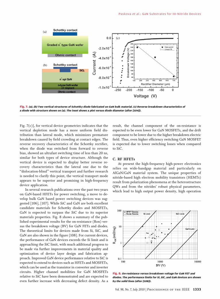
Fig. 7(c)], for vertical device geometries indicates that the
vertical depletion mode has a more uniform field dis-
tribution than lateral mode, which minimizes premature
breakdown caused by field crowding at contact edges. The
reverse recovery characteristics of the Schottky rectifier,when the diode was switched from forward to reverse
bias, showed an ultrafast switching time of less than 20 ns,
similar for both types of device structure. Although the
vertical device is expected to display better reverse re-
covery characteristics than the lateral one due to the
Bdislocation-blind[ vertical transport and further research
is needed to clarify this point, the vertical transport mode
appears to be superior and promising in high-frequencydevice application.
In several research publications over the past two years
on GaN-based HFETs for power switching, a move to de-
velop bulk GaN based power switching devices was sug-
gested [106], [107]. While SiC and GaN are both excellent
candidate materials for Schottky diodes and MOSFETs,
GaN is expected to surpass the SiC due to its superior
materials properties. Fig. 8 shows a summary of the pub-lished experimental results for the on-resistance (Ron) ver-
sus the breakdown voltage (BV) for GaN FETs and diodes.
The theoretical limits for devices made from Si, SiC, and
GaN are also shown in the figure [108]. For current devices,
the performance of GaN devices exceeds the Si limit and is
approaching the SiC limit, with much additional progress to
be made via further improvements in material quality and
optimization of device layer design and fabrication ap-proach. Improved GaN device performance relative to SiC is
expected to extend to devices such as HFETs and MOSFETs,
which can be used as the transistor in converter and inverter
circuits. Higher channel mobilities for GaN MOSFETs
relative to SiC have been demonstrated and are expected to
even further increase with decreasing defect density. As a
result, the channel component of the on-resistance is
expected to be even lower for GaN MOSFETs, and the drift
component to be lower due to the higher breakdown electric
field. Thus, even higher efficiency switching GaN MOSFET
is expected due to lower switching losses when comparedto SiC.
C. RF HFETsAt present the high-frequency high-power electronics
relies on wide-bandgap material and particularly on
AlGaN/GaN material system. The unique properties of
nitride-based high electron mobility transistors (HEMTs)
result from polarization phenomena at the heterostructure
QWs and from the nitrides’ robust physical parameters,
which lead to high output power density, high operation
Fig. 8. On-resistance versus breakdown voltage for GaN FET and
diodes. The performance limits for Si, SiC, and GaN devices are shown
by the solid lines (after [108]).
Fig. 7. (a), (b) Two vertical structures of Schottky diode fabricated on GaN bulk material. (c) Reverse breakdown characteristics of
a diode with structure shown on (a). The inset shows a plot versus diode diameter (after [104]).
Paskova et al. : GaN Substrates for III-Nitride Devices
Vol. 98, No. 7, July 2010 | Proceedings of the IEEE 1333

voltage, and high input impedance due to unique pro-
perties of GaN, such as high breakdown voltage and large
bandgap. Owing to the piezoelectric and spontaneous po-
larization, AlGaN/GaN HFETs grown on c-plane sapphire
or SiC have two-dimensional electron gas (2DEG)densities of �1� 1013 cm�2, even without doping the
barriers [109]. Moreover, by increasing the Al composi-
tion in the barrier, the sheet carrier density can be
increased further, which is desirable for high-power
high-frequency applications [110]. When a thin (of about
7 nm) AlN barrier is used, 2DEG densities could be as
high as 5 � 1013 cm�2, which is near the polarization
limit [111]. However, for Al compositions larger than 40%,due to the large lattice mismatch between GaN and
AlGaN, inferior barrier quality significantly reduces the
mobility [112] and therefore the device performance. To
address this issue, Kuzmık proposed using a nearly lattice-
matched AlInN/GaN material system to improve the
performance of HFETs with high sheet carrier densities
provided by spontaneous polarization only [113], [114]. So
far, the growth on lattice-mismatched substrates (sapphire,SiC) was unavoidable [Fig. 9(a)], and the resulting layers
contain a large number of threading dislocations. To
address this issue, use of high-quality substrates with a
low dislocation density is needed. The large-scale semi-
insulating GaN templates with reduced dislocation density
may be one solution to the material quality problem, but
not necessarily sufficient due to the remaining strain-
induced defects in growth on foreign sapphire, as well asremaining sapphire with very low thermal conductivity.
Therefore, eliminating the foreign substrate is needed, so
that higher quality native bulk substrate material with high
thermal conductivity can be used to enhance the device
performance [Fig. 9(c)].
There is a small but growing number of studies
investigating the use of semi-insulating GaN substrates
for radio-frequency (RF) HEMT applications [114]–[118].
Researchers at the U.S. Naval Research Laboratories have
grown via MBE AlGaN/GaN HEMTs on semi-insulatingGaN substrates [116], [117]. Comparative analysis revealed
that for all device metrics examined, the performance of
HEMTs on GaN substrates relative to those on SiC was
improved. Fig. 9(c) shows device performance character-
istics, including an off-state breakdown voltage in excess of
200 V, low gate leakage, and an output power density
over 5 W/mm at 4 GHz and 4.8 W/mm at 10 GHz.
Microwave measurements on 0.45 mm gate-length devicesyielded fT and fMAX of 36 and 56 GHz, respectively,
demonstrating excellent device performance attainable by
RFplasma-assisted MBE grown HEMTs on low dislocation
density HVPE-GaN substrates. Another study showed
9.4 W/mm at 10 GHz for HEMTs on GaN substrates with
improved reliability when compared to similar devices on
SiC substrates [118]. The improved performance of nitride-
based HEMTs is promising for their potential wide ap-plication in satellite broadcast equipment, mobile phones,
GPS navigation systems, broadband wireless access sys-
tems, and other core technologies fundamental to our
information-driven society.
VI. SUMMARY
Native bulk GaN substrates have been intensivelydeveloped by several growth techniques. Availability of
this material is constantly increasing in amount, size,
doping, and orientation alternatives. Their use in device
growth is proven as beneficial for improvement of the
performance of all devices under consideration and for
Fig. 9. Typical structure of HEMT grown on (a) foreign substrate and (b) semi-insulating GaN substrate. Output power, gain,
and power-added efficiency at 4 GHz of device with 150-�m-wide gate (after [115]).
Paskova et al. : GaN Substrates for III-Nitride Devices
1334 Proceedings of the IEEE | Vol. 98, No. 7, July 2010

device production cost reduction for some devices. Furtherimprovement of the substrate quality, along with increasing
size and decreasing cost, is expected in the near future,
which will in turn influence the device quality and cost. h
Acknowledgment
The authors would like to thank their many U.S.
Department of Defense and Department of Energy
supporters and their collaborators, including K.Y. Lai,J. Grenko, and M. A. L. Johnson (North Carolina State
University); Y. Zhou and M. Park (Auburn University);
T. Detchprohm and C. Wetzel (Rensselaer Polytechnic
Institute); R. Dupuis (Georgia Technology Institute);
and D. F. Storm (Naval Research Laboratory) for
realization and characterization of the devices grown on
Kyma GaN bulk substrates and for many fruitful
discussions.
RE FERENCES
[1] R. Cadoret and A. Trasoidaine, BGrowth ofGaN by HVPE,[ J. Phys. Condens. Matter,vol. 13, pp. 6893–6905, 2001.
[2] A. Koukitu, S. Hama, T. Taki, and H. Seki,BThermodynamic analysis of hydridevapour-phase epitaxy of GaN,[ Jpn. J.Appl. Phys., vol. 37, p. 762, 1998.
[3] A. S. Segal, A. V. Kondratyev, S. Y. Karpov,D. Martin, V. Wagner, and M. Ilegems,BHydride epitaxial GaN simulator HepiGaNSfrom semiconductor technology research,[J. Cryst. Growth, vol. 270, p. 384, 2004.
[4] C. E. C. Dam, A. P. Grzegorczyk,P. R. Hageman, R. Dorsman, C. R. Kleijn,and P. K. Larsen, BThe effect of HVPEreactor geometry on GaN growth rate:Experiments versus simulations,[ J. Cryst.Growth, vol. 271, p. 192, 2004.
[5] E. Richter, C. Hennig, U. Zeimer, L. Wang,M. Weyers, and G. Trankle, BN-type dopingof HVPE grown GaN using dichlorosilane,[Phys. Stat. Sol. (a), vol. 203, no. 7,pp. 1658–1662, 2006.
[6] A. V. Fomin, A. E. Nikolaev, I. P. Nikitina,A. S. Zubrilov, M. G. Mynbaeva,N. I. Kuznetzov, A. P. Kovarsky, B. J. Ber,and D. V. Tsvetkov, BProperties of Si dopedGaN layers grown by HVPE,[ Phys. Stat.Sol. (a), vol. 188, no. 1, pp. 433–437,2001.
[7] G. Jacob, M. Boulou, and M. Furtado,BEffect of growth parameters on theproperties of GaN:Zn epilayers,[ J. Cryst.Growth, vol. 42, p. 136, 1977.
[8] O. Lagerstedt and B. Monemar,BLuminescence in epitaxial GaN:Cd,[J. Appl. Phys., vol. 45, p. 2266, 1974.
[9] C. G. Van de Walle, S. Limpijumnong, andJ. Neugebauer, BFirst principles studies ofberyllium doping of GaN,[ Phys. Rev. B,vol. 63, p. 245205, 2001.
[10] A. Usikov, O. Kovalenkov, V. Ivantsov,V. Sukhoveev, V. Dmitriev, N. Shmidt,D. Poloskin, V. Petrov, and V. Ratnikov,BP-type GaN epitaxial layers and AlGaN/GaNheterostructures with high hole concentrationand mobility grown by HVPE,[ Proc. MRSSymp., vol. 831, p. 453, 2005.
[11] J. Neugebauer and C. G. Van de Walle,BHydrogen in GaN: Novel aspect of acommon impurity,[ Phys. Rev. Lett.,vol. 75, p. 4452, 1995.
[12] R. P. Vaudo, X. Xu, A. Salant, J. Malkarne,and G. R. Brandes, BCharacteristics ofsemi-insulating Fe doped GaN substrates,[Phys. Stat. Sol. (a), vol. 200, no. 1, pp. 18–21,2003.
[13] T. Paskova, E. A. Preble, A. D. Hanser,K. R. Evans, R. Kroeger, P. P. Paskov,A. J. Cheng, M. Park, J. A. Grenko, andM. A. L. Johnson, BPolar and nonpolar HVPEGaN substrates: Impact of doping on thestructural, electrical and optical
characteristics,[ Phys. Stat. Sol., vol. 6,pp. S344–S347, 2009.
[14] T. Detchprohm, K. Hiramatsu, H. Amano,and I. Akasaki, BHydride vapor phaseepitaxial growth of a high quality GaN filmsusing a ZnO buffer layers,[ Appl. Phys. Lett.,vol. 61, no. 22, p. 2688, 1992.
[15] R. J. Molnar, W. Gotz, L. T. Romano, andJ. M. Johnson, BGrowth of gallium nitride byhydride vapor epitaxy,[ J. Cryst. Growth,vol. 178, pp. 147–156, 1997.
[16] T. Paskova, J. Birch, S. Tungasmita,R. Beccard, M. Heuken, E. B. Svedberg,P. Runesson, E. M. Goldys, and B. Monemar,BThick hydride vapor phase epitaxial GaNlayers grown on sapphire with differentbuffers,[ Phys. Stat. Sol. (a), vol. 176,pp. 415–419, 1999.
[17] T. Paskova, S. Tungasmita, E. Valcheva,E. Svedberg, B. Arnaudov, S. Evtimova,P. Persson, A. Henry, R. Beccard,M. Heuken, and B. Monemar, BHydridevapor phase homoepitaxial growth of GaNon MOCVD grown templates,[ MRS InternetJ. Nitride Semicond. Res., vol. 5S1, p. W3.14,2000.
[18] T. Paskova, E. Valcheva, J. Birch,S. Tungasmita, P. O. A. Persson, P. P. Paskov,S. Evtimova, M. Abrashev, and B. Monemar,BDefect and stress relaxation in HVPE-GaNfilms using high temperature reactivelysputtered AlN buffer,[ J. Cryst. Growth,vol. 230, pp. 381–386, 2001.
[19] Y. Oshima, T. Eri, H. Sunakawa, and A. Usui,BFabrication of freestanding GaN wafersby hydride vapor phase epitaxy withvoid-assisted separation,[ Phys. Stat.Sol. (a), vol. 194, no. 2, pp. 554–558,2002.
[20] O. Parillaud, V. Wagner, H. J. Buehlmann,and M. Ilegems, BLocalized epitaxy of GaNby HVPE on SiC and sapphire substrates,[MRS Int. J. Nitride Semicond. Res., vol. 4S1,p. G4.3, 1999.
[21] A. Usui, H. Sunakawa, A. Sakai, andA. A. Yamaguchi, BThick GaN epitaxialgrowth with low dislocation density byhydride vapor phase epitaxy,[ Jpn. J. Appl.Phys., vol. 36, pp. L899–L902, 1997.
[22] H. Sone, S. Nambu, Y. Kawaguchi,M. Yamaguchi, H. Miyake, K. Hiramatsu,Y. Iyechika, T. Maeda, and N. Sawaki,BOptical and crystalline properties ofepitaxial-overgrown-GaN using tangstenmask by hydride vapor phase epitaxy,[Jpn. J. Appl. Phys., vol. 38, pp. L356–L359,1999.
[23] D. R. Ketchum and J. W. Kolis, BCrystalgrowth of gallium nitride in supercriticalammonia,[ J. Cryst. Growth, vol. 222,pp. 431–434, 2001.
[24] R. Dwilinski, R. Doradzinski, J. Garczynski,L. Sierzputowski, J. M. Baranowski, andM. Kaminska, BAMMONO method for GaN
and AlN production,[ Diamond Rel. Mater.,vol. 7, pp. 1348–1350, 1998.
[25] B. Wang and M. Callahan, BTransportgrowth of GaN crystals by theammonothermal technique usingvarious nutrients,[ J. Cryst. Growth,vol. 291, pp. 455–460, 2006.
[26] T. Hashimoto, K. Fujito, F. Wu, B. Haskell,P. T. Fini, J. S. Speck, and S. Nakamura,BStructural characterization of thick GaNfilms grown on free-standing GaN ssedsby ammonotherma method using basicammonia,[ Jpn. J. Appl. Phys., vol. 44, no. 25,pp. L797–L799, 2005.
[27] D. R. Ketchum and J. W. Kolis, BCrystalgrowth of gallium nitride in supercriticalammonia,[ Proc. Mater. Res. Soc. Symp.,vol. 495, pp. 367–371, 1998.
[28] T. Fukuda and D. Ehrentraut, BProspectsfor ammonothermal growth of largeGaN crystals,[ J. Cryst. Growth, vol. 305,p. 304–310, 2007.
[29] M. P. D’Evelyn, H. C. Hong, D.-S. Park,H. Lu, E. Kaminsky, R. R. Melkote,P. Perlin, M. Lesczynski, S. Porowski, andR. J. Molnar, BBulk GaN crystal growthby the high-pressure ammonothermalmethod,[ J. Cryst. Growth, vol. 300,pp. 11–16, 2007.
[30] R. Dwilinski, R. Doradzinski, J. Garczynski,L. P. Sierzputowski, A. Puchalski,Y. Kanbara, K. Yagi, H. Minakuchi, andH. Hayashi, BExcellent crystallinity oftruly bulk ammonothermal GaM,[ J. Cryst.Growth, vol. 310, pp. 3911–3916, 2008.
[31] H. Yamane, M. Shimada, T. Sekiguchi, andF. J. DiSalvo, BMorphology andcharacterization of GaN single crystalsgrown in Na flux,[ J. Cryst. Growth, vol. 186,p. 8–12, 1998.
[32] F. Kawamura, H. Umeda, M. Kawahara,M. Yoshimura, Y. Mori, T. Sasaki, H. Okado,K. Arakawa, and H. Mori, BDrastic decreasein dislocation during liquid phase epitaxygrowth of GaN single crystals using Na fluxmethod without any artificial processes,[Jpn. J. Appl. Phys., vol. 45, pp. 2528–2530,2006.
[33] F. Kawamura, M. Morishita, M. Tanpo,M. Imade, M. Yoshimura, Y. Kitaoka,Y. Mori, and T. Sasaki, BEffect of carbonadditive on increases in the growth rateof 2 in GaN single crystals in the Na fluxmethod,[ J. Cryst. Growth, vol. 310,pp. 3946–3949, 2008.
[34] E. Maissner, B. Birkmann, S. Hussy,G. Sun, J. Friedrich, and G. Mueller,BCharacterization of GaN crystals andepilayers grown from a solution at roompressure,[ Phys. Stat. Sol. (c), vol. 2,pp. 2040–2043, 2005.
[35] B. N. Feigelson, R. M. Frazier, M. Gowda,J. A. Freitas, M. Fatemi, M. A. Mastro, andJ. G. Tischer, BSeeded growth of GaN singlecrystals from solution at near atmospheric
Paskova et al. : GaN Substrates for III-Nitride Devices
Vol. 98, No. 7, July 2010 | Proceedings of the IEEE 1335

pressure,[ J. Cryst. Growth, vol. 310,pp. 3934–3940, 2008.
[36] R. G. Molnar, BHydride vapor phase epitaxialgrowth of III-V nitrides,[ in Galium Nitride(GaN) II: Semicondusctors and Semimetals,vol. 57, J. Pankove and T. Moustakas, Eds.London, U.K.: Academic, 1999, pp. 1–31.
[37] H. Morkoc, BComprehensive characterizationof hydride VPE grown GaN layers andtemplates,[ Mater. Sci. Eng. R, vol. 33,pp. 135–207, 2001.
[38] T. Paskova and B. Monemar, BHydridevapour phase epitaxy growth of thick GaNlayers,[ in III-Nitride Semiconductors:Growth, O. Manasreh, Ed. New York:Taylor & Francis, 2003, pp. 175–236.
[39] W. Zhang and B. K. Meyer, BGrowth of GaNquasi-substrates by hydride vapor phaseepitaxy,[ Phys. Stat. Sol. (c), no. 6,pp. 1571–1582, 2003.
[40] P. Gibart, B. Beaumont, and P. Vennegues,BEpitaxial lateral overgrowth of GaN,[ inNitride Semiconductors, Handbook onMaterials and Devices, P. Ruterana,M. Albrecht, and J. Neugebauer, Eds.Berlin, Germany: Wiley-VCH, 2003,pp. 45–106.
[41] C. Hemmingsson, B. Monemar, Y. Kumagai,and A. Koukitu, BGrowth of III-nitrides withhalide vapor phase epitaxy,[ in Handbook ofCrystal Growth, G. Dhanaraj, K. Byrappa,V. Prasad, and M. Dudley, Eds. Berlin,Germany: Springer-Verlag, 2008.
[42] I. Grzegory, B. `ucznik, M. Bockowski, andS. Porowski, BCrystallization of lowdislocation density GaN by high-pressuresolution and HVPE methods,[ J. Cryst.Growth, vol. 300, pp. 17–25, 2007.
[43] T. Paskova and K. R. Evans, BGaN substrates:Progress, status and prospects,[ IEEE J. Sel.Topics Quantum Electron., vol. 15,pp. 1041–1052, 2009.
[44] R. F. Davis, A. M. Roskowski, E. A. Preble,J. S. Speck, B. Heying, J. A. Freitas, Jr.,E. R. Glaser, and W. E. Carlos, BGalliumnitride materialsVProgress, status andpotential roadblocks,[ Proc. IEEE, vol. 90,no. 6, pp. 993–1004, 2002.
[45] K. Motoki, T. Okahisa, S. Nakahata,N. Matsumoto, H. Kimura, H. Kasai,K. Takemoto, K. Uematsu, M. Ueno,Y. Kumagai, A. Koukito, and H. Seki,BGrowth and characterization offreestanding GaN substrates,[ J. Cryst.Growth, vol. 237–239, pp. 912–921,2002.
[46] O. Kryliouk, M. Reed, T. Dann, T. Anderson,and B. Chai, BLarge area GaN substrates,[Mater Sci. Eng. B, vol. 66, no. 1, pp. 26–29,1999.
[47] E. Richter, C. Hnnig, U. Zeimer, M. Weyers,G. Tranke, P. Reiche, S. Ganschow,R. Uecker, and K. Peters, BFreestandingtwo inch c-plane GaN layers grown on(100)-�-lithium aluminium oxide by hydridevapor phase epitaxy,[ Phys. Stat. Sol. (c),vol. 3, pp. 1439–1443, 2006.
[48] D. Hanser, M. Tutor, E. Preble, M. Williams,X. Xu, D. Tsvetkov, and L. Liu, BSurfacepreparation of substrates from bulk GaNcrystals,[ J. Cryst. Growth, vol. 305,pp. 372–376, 2007.
[49] K. Fujito, S. Kubo, and I. Fujimura,BDevelopment of bulk GaN crystals andnonpolar/semipolar substrate by HVPE,[MRS Bull., vol. 34, pp. 313–317, 2009.
[50] T. Fujimori, BHVPE and ammonothermalGaN substrates for high performancedevices,[ in Plenary Talk at IW on Nitride
Semiconductors, Montreux, Switzerland,Oct. 6–10, 2008.
[51] R. P. Vaudo, X. Xu, C. Loria, A. D. Salant,J. S. Flynn, and G. R. Brandes, BGaN boulegrowth: A pathway to GaN wafer withimproved material quality,[ Phys. Stat.Sol. (a), vol. 194, no. 2, pp. 494–497,2002.
[52] M. Weyers, E. Richter, C. Hennig,S. Hagedorn, T. Wernicke, and G. Trankle,BGaN substrates by HVPE,[ in Proc. SPIE,2008, vol. 6910, pp. 691001.1–691001.10.
[53] D. Hanser, L. Liu, E. A. Preble, D. Thomas,and M. Williams, BGrowth and fabrication of2 inch free-standing GaN substrates via theboule growth method,[ Proc. Mater. Res. Soc.Symp., vol. 798, p. Y2.1.1, 2004.
[54] D. Hanser, L. Liu, E. A. Preble, K. Udwary,T. Paskova, and K. R. Evans, BFabrication andcharacterization of native non-polar GaNsubstrates,[ J. Cryst. Growth, vol. 310,pp. 3953–3956, 2008.
[55] M. Feneberg and K. Thonke, BPolarizationfields of III-nitrides grown in differentcrystal orientations,[ J. Phys. Condens.Matter, vol. 19, p. 403201, 2007.
[56] I. Vurgaftman and J. R. Meyer, BBandparameters of nitrogen containingsemiconductors,[ J. Appl. Phys., vol. 94,p. 3675, 2003.
[57] A. E. Romanov, T. J. Baker, S. Nakamura,and J. S. Speck, BStrain-induced polarizationin wurtzite III-nitride semipolar layers,[J. Appl. Phys., vol. 100, p. 023522, 2006.
[58] F. Bernardini and V. Fiorentini, BFirstprinciple calculation of piezoelectrictensor d of III-V nitrides,[ Appl. Phys.Lett., vol. 80, pp. 4145–4147, 2002.
[59] T. Paskova, BDevelopment and prospects ofnitride materials and devices with nonpolarsurfaces,[ Phys. Stat. Sol. (b), vol. 245, no. 6,pp. 1011–1025, 2008.
[60] B. A. Haskell, S. Nakamura, S. P. DenBaars,and J. S. Speck, BProgress in the growth ofnonpolar gallium nitride,[ Phys. Stat. Sol. (b),vol. 244, no. 8, pp. 2847–2858, 2007.
[61] S. DenBaars, S. Nakamura, J. Speck, andU. Mishra, BRecent breakthroughs innonpolar and semipolar GaN LEDs andlaser diodes,[ in Plenary Talk IW NitrideSemicond., Montreux, Switzerland,Oct. 6–10, 2008.
[62] M.-H. Kim, M. F. Schubert, Q. Dai,J. K. Kim, and E. F. Schubert,BOrigin of efficiency droop in GaN-basedlight-emitting diodes,[ Appl. Phys. Lett.,vol. 91, p. 183507, 2007.
[63] H. Masui, H. Kroemer, M. C. Schmidt,K.-C. Kim, N. N. Fellows, S. Nakamura, andS. P. DenBaars, BElectroluminescenceefficiency of (10-10)-oriented InGaN-basedlight-emitting diodes at low temperature,[J. Phys. D Appl. Phys., vol. 41, p. 082001,2008.
[64] M. Kunzer, M. Baeumler, K. Kohler,C.-C. Leancu, U. Kaufmann, and J. Wagner,BInjection level dependent luminescencecharacteristics of UV-violet emitting(AlGaIn)N LED structures,[ Phys. Stat.Sol. (a), vol. 204, p. 236, 2007.
[65] Y. C. Shen, G. O. Mueller, S. Watanabe,N. F. Gardner, A. Munkholm, andM. R. Krames, BAuger recombination inInGaN measured by photoluminescence,[Appl. Phys. Lett., vol. 91, p. 141101,2007.
[66] Y. Yang, X. A. Cao, and C. Yan,BInvestigation of the nonthermal mechanismof efficiency rolloff in InGaN light-emitting
diodes,[ IEEE Trans. Electron Devices, vol. 55,p. 1771, 2008.
[67] I. Ho and G. B. Stringfellow, BSolid phaseimmiscibility in GaInN,[ Appl. Phys. Lett.,vol. 69, p. 2701, 1996.
[68] Y.-H. Cho, S. K. Lee, H. S. Kwack, J. Y. Kim,K. S. Lim, T. W. Kang, M. S. Seon,O. H. Nam, and Y. J. Park, BCarrierloss and luminescence degradation ingreen-light-emitting InGaN quantumwells with micron-scale indium clusters,[Appl. Phys. Lett., vol. 83, pp. 2578–2580,2003.
[69] Y. Chen, T. Takeuch, H. Amano, I. Akasaki,N. Yamada, Y. Kaneko, and S. Y. Wang,BPit formation in GaInN quantum wells,[Appl. Phys. Lett., vol. 72, pp. 710–712,1998.
[70] C. Wetzel, T. Salagaj, T. Detchprohm, P. Li,and J. S. Nelson, BGaInN/GaN growthoptimization for high-power greenlight-emitting diodes,[ Appl. Phys. Lett.,vol. 85, pp. 866–868, 2004.
[71] S. Porowski, BBlue lasers on high pressuregrown GaN single crystal substrates,[Europhys. News, vol. 35, no. 3, 2004.
[72] G. Parish, S. Keller, P. Kozodoy,J. P. Ibbetson, H. Marchand, P. T. Fini,S. B. Fleischer, S. P. DenBaars, U. K. Mishra,and Tarsa, BHigh-performance(Al,Ga)N-based solar-blind ultravioletp–i–n detectors on laterally epitaxiallyovergrown GaN,[ Appl. Phys. Lett., vol. 75,pp. 247–249, 1999.
[73] S. Figge, T. Bottcher, J. Dennemarck,R. Kroger, T. Paskova, B. Monemar, andD. Hommel, BOptoelectronic deviceson bulk GaN,[ J. Cryst. Growth, vol. 281,pp. 101–106, 2005.
[74] N. Narendran, Y. Gu, J. P. Freyssinier,H. Yu, and L. Deng, BSolid-state lighting:Failure analysis of white LEDs,[ J. Cryst.Growth, vol. 268, pp. 449–456, 2004.
[75] J. Senawiratne, Y. Li, M. Zhu, Y. Xia,W. Zhao, T. Detchprohm, A. Chatterjee,J. L. Plawsky, and C. Wetzel, BJunctiontemperature measurements and thermalmodeling of GaInN/GaN quantum welllight-emitting diodes,[ J. Electron Mater.,vol. 37, no. 5, pp. 607–610, 2008.
[76] O. H. Nam, K. H. Ha, J. S. Kwak, S. N. Lee,K. K. Choi, T. H. Chang, S. H. Chae,W. S. Lee, Y. J. Sung, H. S. Paek, J. H. Chae,T. Sakong, J. K. Son, H. Y. Ryu, Y. H. Kim,and Y. Park, BCharacteristics of GaN-basedlaser diodes for post-DVD applications,[Phys. Stat. Sol. (a), vol. 201, no. 12,pp. 2717–2720, 2004.
[77] T. Miyoshi, S. Masui, T. Okada,T. Yanamoto, T. Kozaki, S. Nagahama, andT. Mukai, B510–515 nm InGaN-based greenlaser diodes on c-plane GaN substrates,[Appl. Phys. Express, vol. 2, p. 062201, 2009.
[78] K. Y. Lai, T. Paskova, G. Wheeler, J. Grenko,M. A. L. Johnson, D. Barlage, K. Udwary,E. Preble, and K. R. Evans, BExcitationcurrent dependent cathodoluminescencestudy of InGaN/GaN quantum wells grownon m-plane and c-plane GaN substrates,[J. Appl. Phys., vol. 106, no. 11, 2009.
[79] C. Chen, V. Adivarahan, J. Yang,M. Shatalov, E. Kuokstis, and M. A. Kahn,BUltraviolet light emitting diodes usingnon-polar a-plane gan-algan multiplequantum wells,[ Jpn. J. Appl. Phys.,vol. 42, no. 9, pp. L11039–L11040,2003.
[80] A. Chakraborty, S. Keller, C. Meier,B. A. Haskell, S. Keller, P. Waltereit,S. P. DenBaars, S. Nakamura, J. S. Speck, and
Paskova et al. : GaN Substrates for III-Nitride Devices
1336 Proceedings of the IEEE | Vol. 98, No. 7, July 2010

U. K. Mishra, BProperties of nonpolara-plane InGaN/GaN multiple quantum wellsgrown on lateral epitaxially overgrowna-plane GaN,[ Appl. Phys. Lett., vol. 86,p. 031901, 2005.
[81] A. Chakraborty, T. B. Baker, B. A. Haskell,W. Fu, J. S. Speck, S. P. DenBaars,S. Nakamura, and U. K. Mishra, BMilliwattpower blue InGaN/GaN light-emittingdiodes on semipolar GaN templates,[Jpn. J. Appl. Phys., vol. 44, no. 30,pp. L945–L947, 2005.
[82] A. Chakraborty, B. A. Haskell, H. Masui,S. Keller, J. S. Speck, S. P. DenBaars,S. Nakamura, and U. K. Mishra,BNonpolar m-Plane blue-light-emittingdiode lamps with output powerof 23.5 mWunder pulsed operation,[ Jpn. J. Appl. Phys.,vol. 45, no. 2A, pp. L739–L741, 2006.
[83] C. Wetzel, M. Zhu, J. Senawiratne,T. Detchprohm, P. D. Persans, E. A. Preble,and D. Hanser, BLight-emitting diodedevelopment on polar and non-polar GaNsubstrates,[ J. Cryst. Growth, vol. 310,pp. 3987–3991, 2008.
[84] R. Sharma, P. M. Pattison, H. Masui,R. M. Farrell, T. J. Baker, B. A. Haskell,F. Wu, S. P. DenBaars, J. S. Speck, andS. Nakamura, BDemonstration of a semipolar(10-1-3) InGaN/GaN green light emittingdiode,[ Appl. Phys. Lett., vol. 87, p. 231110,2005.
[85] M. C. Schmidt, K. C. Kim, H. Sato,N. Fellows, H. Masui, S. Nakamura,S. P. DenBaars, and J. S. Speck, BHigh powerand high external efficiency m-plane InGaNlight emitting diodes,[ Jpn. J. Appl. Phys.,vol. 46, p. L126, 2007.
[86] A. Tyagi, H. Zhong, N. N. Fellows, M. Iza,J. S. Speck, S. P. DenBaars, and S. Nakamura,BHigh brightness violet InGaN/GaN lightemitting diodes on semipolar (10-1-1)bulk GaN substrate,[ Jpn. J. Appl. Phys.,vol. 46, no. 7, p. L129, 2007.
[87] H. Zhong, A. Tyagi, N. N. Fellows,F. Wu, R. B. Chung, M. Saito, K. Fujito,J. S. Speck, S. P. DenBaars, and S. Nakamura,BHigh power and high efficiency greenlight emitting diode on free-standingsemipolar (10-11) bulk GaN substrate,[Appl. Phys. Lett., vol. 90, p. 233504,2007.
[88] K. Iso, H. Yamada, H. Hirasawa,N. N. Fellows, M. Saito, K. Fujito,S. P. DenBaars, J. S. Speck, and S. Nakamura,BHigh brightness blue InGaN/GaN lightemitting diode on nonpolar m-plane bulkGaN substrate,[ Jpn. J. Appl. Phys., vol. 46,p. L960, 2007.
[89] H. Sato, A. Tyagi, H. Zhong, N. N. Fellows,R. B. Chung, M. Saito, K. Fujito, J. S. Speck,S. P. DenBaars, and S. Nakamura, BHighpower and high efficiency green lightemitting diode on free-standing semipolar(10-22) bulk GaN substrate,[ Phys. Stat.Sol. (rrl), vol. 1, no. 4, pp. 162–164,2007.
[90] M. C. Schmidt, K. C. Kim, R. M. Farrell,D. F. Feezell, D. A. Cohen, M. Saito,K. Fujito, J. S. Speck, S. P. DenBaars, andS. Nakamura, BDemonstration of nonpolarm-plane InGaN/GaN laser diodes,[ Jpn. J.Appl. Phys., vol. 46, p. L190, 2007.
[91] K. Okamoto, H. Ohta, S. F. Chichibu,J. Ichihara, and J. Takasu, BContinuous-waveoperation of m-plane InGaN multiple
quantum well laser diodes,[ Jpn. J. Appl.Phys., vol. 46, p. L187, 2007.
[92] D. F. Feezell, M. C. Schmidt, R. M. Farrell,K. C. Kim, M. Saito, K. Fujito, D. A. Cohen,J. S. Speck, S. P. DenBaars, and S. Nakamura,BAlGaN-cladding-free nonpolar InGaN/GaNlaser diodes,[ Jpn. J. Appl. Phys., vol. 46,p. L284, 2007.
[93] A. Tyagi, H. Zhong, R. B. Chung,D. F. Feezell, M. Saito, K. Fujito, J. S. Speck,S. P. DenBaars, and S. Nakamura,BSemipolar (10-1-1) InGaN/GaN laser diodeon bulk GaN substrate,[ Jpn. J. Appl. Phys.,vol. 46, p. L444, 2007.
[94] R. M. Farrell, D. F. Feezell, M. C. Schmidt,D. A. Haeger, K. M. Kelchner, K. Iso,H. Yamada, M. Saito, K. Fujito, D. A. Cohen,J. S. Speck, S. P. DenBaars, and S. Nakamura,BContinuous-wave operation ofAlGaN-cladding-free nonpolar m-planeInGaN/GaN laser diodes,[ Jpn. J. Appl. Phys.,vol. 46, p. L761, 2007.
[95] K. Okamoto, T. Tanaka, M. Kubota, andH. Ohta, BPure blue laser diodes on nonpolarm-plane GaN with InGaN waveguidinglayers,[ Jpn. J. Appl. Phys., vol. 46, p. L820,2007.
[96] K. Kojima, M. Funato, Y. Kawakami,S. Masui, S. Nagahama, and T. Mukai,BStimilated emission at 474 nm from anInGaN laser diode structure grown on(11-22) GaN substrate,[ Appl. Phys. Lett.,vol. 91, p. 251107, 2007.
[97] M. Kubota, K. Okamoto, T. Tanaka, andH. Ohta, BContinuous-wave operation ofblue laser diodes based on nonpolar m-planeggallium nitride,[ Appl. Phys. Express, vol. 1,p. 011102, 2008.
[98] Y. Tsuda, M. Ohta, P. O. Vaccaro, S. Ito,S. Hirukawa, Y. Kawaguchi, Y. Fujishiro,Y. Takahira, Y. Ueta, T. Takakura, andT. Yuasa, BBlue laser diodes fabricatedon m-plane GaN substrates,[ Appl. Phys.Express, vol. 1, p. 011104, 2008.
[99] K. Okamoto, T. Tanaka, and M. Kubota,BHigh-efficiency continuous-waveoperation of blue-green laser diodes basedon nonpolar m-plane gallium nitride,[Appl. Phys. Express, vol. 1, p. 072201,2008.
[100] K. Okamoto, J. Kasiwagi, T. Tanaka, andM. Kubota, BNonpolar m-plane InGaNmultiple quantum well laser diodeswith a lasing wavelength of 499.8 nm,[Appl. Phys. Lett., vol. 94, p. 071105,2009.
[101] J. W. P. Hsu, M. J. Manfra, R. J. Molnar,B. Heying, and J. S. Speck, BDirect imagingof reverse-bias leakage through purescrew dislocations in GaN films grownby molecular beam epitaxy on GaNtemplates,[ Appl. Phys. Lett., vol. 81, p. 79,2002.
[102] B. B. Simpkins, E. T. Yu, P. Waltereit, andJ. S. Speck, BCorrelated scanning Kelvinprobe and conductive atomic forcemicroscopy studies of dislocations ingallium nitride,[ J. Appl. Phys., vol. 94,p. 1448, 2003.
[103] K. H. Baik, Y. Irokawa, J. Kim,J. R. LaRoche, F. Ren, S. S. Park,Y. J. Park, and S. J. Pearton, B160-A bulkGaN Schottky diode array,[ Appl. Phys. Lett.,vol. 83, p. 3192, 2003.
[104] Y. Zhou, M. Li, D. Wang, C. Ahyi,C.-C. Tin, J. Williams, M. Park,
N. M. Williams, and A. Hanser,BElectrical characteristics of bulk GaN-basedSchottky rectifiers with ultrafast reverserecovery,[ Appl. Phys. Lett., vol. 88,p. 113509, 2006.
[105] H. Lu, R. Zhang, X. Xiu, Z. Xie, Y. Zheng,and Z. Li, BLow leakage Schottky rectifiersfabricated on homoepitaxial GaN,[ Appl.Phys. Lett., vol. 91, p. 172 113, 2007.
[106] T. Uesugi, BPower devices for automotiveapplicationsVReviews of technologiesfor low power dissipation and highruggedness,[ R&D Rev. Toyota CRDL,vol. 35, p. 1, 2006.
[107] H. Ueda, M. Sugimoto, T. Uesugi, andT. Kachi, BWide-bandgap semiconductorsfor automobile applications,[ in CSMANTECH Conf., Vancouver, BC, Canada,Apr. 24–27, 2006.
[108] S. J. Pearton and F. Ren, BGaN electronics,[Adv. Mater., vol. 12, p. 1571, 2000.
[109] H. Morkoc, Handbook of NitrideSemiconductors and Devices. Berlin,Germany: Wiley-VCH, 2008.
[110] Y.-F. Wu, B. P. Keller, P. Fini, S. Keller,T. J. Jenkins, L. T. Kehias, S. P. DenBaars,and U. K. Mishra, BHigh Al-contentAlGaN/GaN MODFET’s for ultrahighperformance,[ IEEE Electron Device Lett.,vol. 19, no. 2, pp. 50–53, 1998.
[111] Y. Cao and D. Jena, BHigh-mobility windowfor two-dimensional electron gases atultrathin AlN/GaN heterojunctions,[ Appl.Phys. Lett., vol. 90, p. 182 112, 2007.
[112] S. Arulkumaran, T. Egawa, H. Ishikawa, andT. Jimbo, BCharacterization ofdifferent-Al-content AlGaN/GaNheterostructures and high-electron-mobilitytransistors on sapphire,[ J. Vac. Sci.Technol. B, vol. 21, p. 888, 2003.
[113] J. Kuzmık, BPower electronics onInAlN/(In)GaN: Prospects for recordperformance,[ IEEE Electron Device Lett.,vol. 22, p. 510, 2001.
[114] J. Kuzmık, BInAlN/(In)GaN high electronmobility transistors: Some aspects of thequantum well heterostructure proposal,[Semicond. Sci. Technol., vol. 17, p. 540, 2002.
[115] W. Huang, T. Khan, and T. P. Chow,BEnhancement-mode n-channel GaNMOSFETs on p and n-GaN/sapphiresubstrates,[ IEEE Electron Device Lett.,vol. 27, p. 796, 2006.
[116] D. F. Storm, D. S. Katzer, J. A. Roussos,J. A. Mittereder, R. Bass, S. C. Binari,D. Hanser, E. A. Preble, and K. R. Evans,BAlGaN/GaN HEMTs on free-standingGaN substrates: MBE growth andmicrowave characterization,[ J. Cryst.Growth, vol. 301–302, pp. 429–433, 2007.
[117] D. F. Storm, D. S. Katzer, J. A. Roussos,J. A. Mittereder, R. Bass, S. C. Binari,L. Zhou, D. J. Smith, D. Hanser,E. Preble, and K. R. Evans, BMicrowaveperformance and structural characterizationof MBE-grown AlGaN/GaN HEMTs onlow dislocation density GaN substrates,[J. Cryst. Growth, vol. 305, p. 340, 2007.
[118] K. K. Chu, P. C. Chao, M. T. Pizzella, R. Actis,D. E. Meharry, K. B. Nichols, R. P. Vaudo,X. Xu, J. S. Flynn, J. Dion, and G. R. Brandes,B9.4-W/mm power density AlGaN GaNHEMTs on free-standing GaN substrates,[IEEE Electron Device Lett., vol. 25, p. 596,2004.
Paskova et al. : GaN Substrates for III-Nitride Devices
Vol. 98, No. 7, July 2010 | Proceedings of the IEEE 1337
ABOUT THE AUT HORS
Tanya Paskova received the Ph.D. degree in
physics from the University of Sofia, Bulgaria,
in 1993.
She was an Assistant Professor at the Univer-
sity of Sofia; and a Visiting Lecturer and Associate
Professor at Linkoping University, Sweden, and
the University of Bremen, Germany. She is
currently Chief Scientist with Kyma Technologies,
Inc., Raleigh, NC. She is an Adjunct Professor at
North Carolina State University. Her research
interests are focused on development of GaN epitaxial growth for
substrate applications and study of basic properties of nitride materials
and structures. She has authored more than 200 scientific papers,
reviews, chapters, and invited talks at international forums and
university seminars and has edited two books.
Drew A. Hanser received the B.S. degree in
ceramic engineering from the University of
Missouri, Rolla, in 1992 and the Ph.D. degree in
materials science and engineering from North
Carolina State University, Raleigh, in 1998.
He was a Research Engineer, Director of
Research and Development, and, most recently,
Chief Technology Officer with Kyma Technologies,
Inc., Raleigh. His research interests are in the
development of growth processes for epitaxial
and bulk III-nitrides and their applications in optical and electronic
devices. He has authored or coauthored more than 50 scientific pub-
lications including papers, invited talks, and book chapters. He is a
member of the Executive Committee for the International Conference on
Compound Semiconductor Manufacturing Technology.
Dr. Hanser is a member of the Materials Research Society.
Keith R. Evans received the B.A. degree in
chemistry from Miami University, Oxford, OH, in
1978 and the Ph.D. degree in physical chemistry
from Purdue University, West Lafayette, IN, in 1984.
He has been President and CEO of Kyma
Technologies, Inc., Raleigh, NC, since 2005. He
previously held executive positions with Crystal IS,
Veeco St. Paul, IQE Inc., and Semiconductor Laser
International. He began his career as a Scientist
with the Air Force Research Laboratories, where
he published more than 200 papers on the growth and characterization
of epitaxial compound semiconductor materials for advanced optoelec-
tronic and electronic device applications. His research interests are
centered on the development of advanced materials technologies for
improving the efficiency and reliability of a broad range of compound
semiconductor devices.
Paskova et al. : GaN Substrates for III-Nitride Devices
1338 Proceedings of the IEEE | Vol. 98, No. 7, July 2010