cgh40025, 25w, gan hemt by cree for general purpose … · 1 subect to change without notice....
TRANSCRIPT

1Subject to change without notice.www.cree.com/wireless
CGH4002525 W, RF Power GaN HEMT
Cree’s CGH40025 is an unmatched, gallium nitride (GaN) high electron mobility
transistor (HEMT). The CGH40025, operating from a 28 volt rail, offers a general
purpose, broadband solution to a variety of RF and microwave applications.
GaN HEMTs offer high efficiency, high gain and wide bandwidth capabilities
making the CGH40025 ideal for linear and compressed amplifier circuits. The
transistor is available in a screw-down, flange package and solder-down, pill
packages.
Rev
4.0
– M
ay 2
015
FEATURES
• Up to 6 GHz Operation
• 15 dB Small Signal Gain at 2.0 GHz
• 13 dB Small Signal Gain at 4.0 GHz
• 30 W typical PSAT
• 62 % Efficiency at PSAT
• 28 V Operation
APPLICATIONS
• 2-Way Private Radio
• Broadband Amplifiers
• Cellular Infrastructure
• Test Instrumentation
• Class A, AB, Linear amplifiers suitable for
OFDM, W-CDMA, EDGE, CDMA waveforms
Package Type: 440196 and 440166PN: CGH40025P and CGH40025F

2 CGH40025 Rev 4.0
Cree, Inc.4600 Silicon Drive
Durham, North Carolina, USA 27703USA Tel: +1.919.313.5300
Fax: +1.919.869.2733www.cree.com/rf
Copyright © 2007-2015 Cree, Inc. All rights reserved. The information in this document is subject to change without notice. Cree and the Cree logo are registered trademarks of Cree, Inc.
Absolute Maximum Ratings (not simultaneous) at 25˚C Case Temperature
Parameter Symbol Rating Units Conditions
Drain-Source Voltage VDSS 84 Volts 25˚C
Gate-to-Source Voltage VGS -10, +2 Volts 25˚C
Storage Temperature TSTG -65, +150 ˚C
Operating Junction Temperature TJ 225 ˚C
Maximum Forward Gate Current IGMAX 7.0 mA 25˚C
Maximum Drain Current1 IDMAX 3 A 25˚C
Soldering Temperature2 TS 245 ˚C
Screw Torque τ 60 in-oz
Thermal Resistance, Junction to Case3 RθJC 4.8 ˚C/W 85˚C
Case Operating Temperature3,4 TC -40, +150 ˚C
Note:1 Current limit for long term, reliable operation2 Refer to the Application Note on soldering at www,wolfspeed.com/RF/Document-Library3 Measured for the CGH40025F at PDISS = 28 W.4 See also, the Power Dissipation De-rating Curve on Page 6.
Electrical Characteristics (TC = 25˚C)
Characteristics Symbol Min. Typ. Max. Units Conditions
DC Characteristics1
Gate Threshold Voltage VGS(th) -3.8 -3.0 -2.3 VDC VDS = 10 V, ID = 7.2 mA
Gate Quiescent Voltage VGS(Q) – -2.7 – VDC VDS = 28 V, ID = 250 mA
Saturated Drain Current IDS 5.8 7.0 – A VDS = 6.0 V, VGS = 2.0 V
Drain-Source Breakdown Voltage VBR 120 – – VDC VGS = -8 V, ID = 7.2 mA
RF Characteristics2 (TC = 25˚C, F0 = 3.7 GHz unless otherwise noted)
Small Signal Gain GSS 12 13 – dB VDD = 28 V, IDQ = 250 mA
Power Output3 PSAT 20 30 – W VDD = 28 V, IDQ = 250 mA
Drain Efficiency4 η 55 62 – % VDD = 28 V, IDQ = 250 mA, PSAT
Output Mismatch Stress VSWR – – 10 : 1 YNo damage at all phase angles, VDD = 28 V, IDQ = 250 mA, POUT = 25 W CW
Dynamic Characteristics
Input Capacitance CGS – 9.0 – pF VDS = 28 V, Vgs = -8 V, f = 1 MHz
Output Capacitance CDS – 2.6 – pF VDS = 28 V, Vgs = -8 V, f = 1 MHz
Feedback Capacitance CGD – 0.4 – pF VDS = 28 V, Vgs = -8 V, f = 1 MHz
Notes:1 Measured on wafer prior to packaging.2 Measured in CGH40025-AMP.3 PSAT is defined as IG = 0.72 mA.4 Drain Efficiency = POUT / PDC

3 CGH40025 Rev 4.0
Cree, Inc.4600 Silicon Drive
Durham, North Carolina, USA 27703USA Tel: +1.919.313.5300
Fax: +1.919.869.2733www.cree.com/rf
Copyright © 2007-2015 Cree, Inc. All rights reserved. The information in this document is subject to change without notice. Cree and the Cree logo are registered trademarks of Cree, Inc.
50
60
70
80
25
30
35
40
Dra
inEf
ficie
ncy
(%)
(W),
Gai
n(d
B)
Psat, Gain, and Drain Efficiency vs Frequency of theCGH40025F in the CGH40025-TB
VDD = 28 V, IDQ = 250 mA
0
10
20
30
40
0
5
10
15
20
3.40 3.45 3.50 3.55 3.60 3.65 3.70 3.75 3.80
Dra
inEf
ficie
ncy
(%)
P SAT
(W),
Gai
n(d
B)
Frequency (GHz)
Psat
Gain
Drain Eff
Typical Performance
Small Signal Gain and Return Loss vs Frequencyof the CGH40025F in the CGH40025-AMP
PSAT, Gain, and Drain Efficiency vs Frequency of theCGH40025F in the CGH40025-AMP
VDD = 28 V, IDQ = 250 mA
Small Signal Gain and Input Return Loss
-25
-20
-15
-10
-5
0
5
10
15
20
2.50 3.00 3.50 4.00 4.50
Frequency (GHz)
Am
plitu
de (d
B)
Small Signal Gain
Input Return Loss
Efficiency
Gain
PSAT
4 CGH40025 Rev 4.0
Cree, Inc.4600 Silicon Drive
Durham, North Carolina, USA 27703USA Tel: +1.919.313.5300
Fax: +1.919.869.2733www.cree.com/rf
Copyright © 2007-2015 Cree, Inc. All rights reserved. The information in this document is subject to change without notice. Cree and the Cree logo are registered trademarks of Cree, Inc.
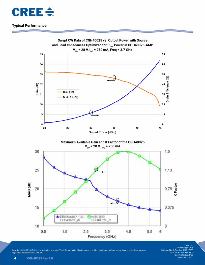
Typical Performance
Swept CW Data of CGH40025 vs. Output Power with Source and Load Impedances Optimized for PSAT Power in CGH40025-AMP
VDD = 28 V, IDQ = 250 mA, Freq = 3.7 GHz
Maximum Available Gain and K Factor of the CGH40025VDD = 28 V, IDQ = 250 mA
MA
G (d
B)
K F
acto
r
Swept CW Data of CGH40025F vs Output Power with Source and Load Impedances Optimized for P3dB in CGH40025F-TB
Vdd = 28 V, Idq = 250 mA, Freq = 3.7 GHz
8
9
10
11
12
13
14
15
20 25 30 35 40 45
Output Power (dBm)
Gai
n (d
B)
0
10
20
30
40
50
60
70
Dra
in E
ffici
ency
(%)
Gain (dB)
Drain Eff. (%)

5 CGH40025 Rev 4.0
Cree, Inc.4600 Silicon Drive
Durham, North Carolina, USA 27703USA Tel: +1.919.313.5300
Fax: +1.919.869.2733www.cree.com/rf
Copyright © 2007-2015 Cree, Inc. All rights reserved. The information in this document is subject to change without notice. Cree and the Cree logo are registered trademarks of Cree, Inc.
Typical Noise Performance
Simulated Minimum Noise Figure and Noise Resistance vs Frequency of the CGH40025FVDD = 28 V, IDQ = 250 mA
Electrostatic Discharge (ESD) Classifications
Parameter Symbol Class Test Methodology
Human Body Model HBM 1A > 250 V JEDEC JESD22 A114-D
Charge Device Model CDM 1 < 200 V JEDEC JESD22 C101-C
Min
imum
Noi
se F
igur
e (d
B)
Noi
se R
esis
tanc
e (O
hms)

6 CGH40025 Rev 4.0
Cree, Inc.4600 Silicon Drive
Durham, North Carolina, USA 27703USA Tel: +1.919.313.5300
Fax: +1.919.869.2733www.cree.com/rf
Copyright © 2007-2015 Cree, Inc. All rights reserved. The information in this document is subject to change without notice. Cree and the Cree logo are registered trademarks of Cree, Inc.
Source and Load Impedances
Frequency (MHz) Z Source Z Load
500 7.75 + j15.5 20 + j5.2
1000 3.11 + j5.72 17 + j6.66
1500 2.86 + j1.63 16.8 + j3.2
2500 2.4 - j3.52 8.02 + j4.32
3500 1.31 - j7.3 5.85 - j0.51
Note 1. VDD = 28V, IDQ = 250mA in the 440166 package.Note 2. Optimized for power gain, PSAT and PAE.Note 3. When using this device at low frequency, series resistors should be used to maintain amplifier stability.
CGH40025 Power Dissipation De-rating Curve
Note 1. Area exceeds Maximum Case Operating Temperature (See Page 2).
D
Z Source Z Load
G
S
20
25
30
Pow
erD
issi
patio
n(W
)
CGH40025F CW Power Dissipation De-rating Curve
0
5
10
15
0 25 50 75 100 125 150 175 200 225 250
Pow
erD
issi
patio
n(W
)
Maximum Case Temperature (°C)
Note 1

7 CGH40025 Rev 4.0
Cree, Inc.4600 Silicon Drive
Durham, North Carolina, USA 27703USA Tel: +1.919.313.5300
Fax: +1.919.869.2733www.cree.com/rf
Copyright © 2007-2015 Cree, Inc. All rights reserved. The information in this document is subject to change without notice. Cree and the Cree logo are registered trademarks of Cree, Inc.
CGH40025-AMP Demonstration Amplifier Circuit Schematic
CGH40025-AMP Demonstration Amplifier Circuit Outline

8 CGH40025 Rev 4.0
Cree, Inc.4600 Silicon Drive
Durham, North Carolina, USA 27703USA Tel: +1.919.313.5300
Fax: +1.919.869.2733www.cree.com/rf
Copyright © 2007-2015 Cree, Inc. All rights reserved. The information in this document is subject to change without notice. Cree and the Cree logo are registered trademarks of Cree, Inc.
CGH40025-AMP Demonstration Amplifier Circuit Bill of Materials
Designator Description Qty
R2 RES,1/16W,0603,1%,47 OHMS 1
R1 RES,1/16W,0603,1%,100 OHMS 1
C6 CAP, 470PF, 5%,100V, 0603 1
C16 CAP, 33 UF, 20%, G CASE 1
C15 CAP, 1.0UF, 100V, 10%, X7R, 1210 1
C8 CAP 10UF 16V TANTALUM 1
C13 CAP, 100.0pF, +/-5%, 0603 1
C1 CAP, 0.8pF, +/-0.1pF, 0603 1
C2 CAP, 0.5pF, +/-0.05pF, 0603 1
C9,C10 CAP, 1.0pF, +/-0.1pF, 0603 2
C4,C11 CAP, 10.0pF,+/-5%, 0603 2
C5,C12 CAP, 39pF, +/-5%, 0603 2
C7,C14 CAP,33000PF, 0805,100V, X7R 2
J3,J4 CONN SMA STR PANEL JACK RECP 2
J1 HEADER RT>PLZ .1CEN LK 5POS 1
- PCB, RO4350B, Er = 3.48, h = 20 mil 1
- CGH40025F or CGH40025P 1
CGH40025F-AMP Demonstration Amplifier Circuit

9 CGH40025 Rev 4.0
Cree, Inc.4600 Silicon Drive
Durham, North Carolina, USA 27703USA Tel: +1.919.313.5300
Fax: +1.919.869.2733www.cree.com/rf
Copyright © 2007-2015 Cree, Inc. All rights reserved. The information in this document is subject to change without notice. Cree and the Cree logo are registered trademarks of Cree, Inc.
Typical Package S-Parameters for CGH40025(Small Signal, VDS = 28 V, IDQ = 100 mA, angle in degrees)
Frequency Mag S11 Ang S11 Mag S21 Ang S21 Mag S12 Ang S12 Mag S22 Ang S22
500 MHz 0.902 -151.72 11.80 92.09 0.025 6.22 0.393 -140.34
600 MHz 0.901 -157.13 9.89 87.31 0.025 2.28 0.402 -143.54
700 MHz 0.900 -161.20 8.49 83.18 0.025 -0.99 0.412 -145.64
800 MHz 0.900 -164.41 7.42 79.49 0.025 -3.82 0.424 -147.11
900 MHz 0.901 -167.04 6.58 76.10 0.024 -6.33 0.436 -148.22
1.0 GHz 0.902 -169.26 5.89 72.93 0.024 -8.60 0.449 -149.12
1.1 GHz 0.903 -171.19 5.33 69.93 0.024 -10.69 0.462 -149.91
1.2 GHz 0.904 -172.89 4.86 67.07 0.023 -12.61 0.476 -150.65
1.3 GHz 0.905 -174.43 4.45 64.33 0.023 -14.39 0.489 -151.38
1.4 GHz 0.906 -175.84 4.10 61.68 0.022 -16.06 0.503 -152.12
1.5 GHz 0.907 -177.14 3.80 59.12 0.022 -17.61 0.517 -152.87
1.6 GHz 0.909 -178.36 3.54 56.64 0.022 -19.05 0.531 -153.65
1.7 GHz 0.910 -179.52 3.30 54.22 0.021 -20.38 0.545 -154.46
1.8 GHz 0.912 179.38 3.09 51.87 0.021 -21.62 0.558 -155.29
1.9 GHz 0.913 178.33 2.90 49.58 0.020 -22.75 0.571 -156.15
2.0 GHz 0.914 177.30 2.73 47.34 0.020 -23.78 0.584 -157.04
2.1 GHz 0.916 176.31 2.58 45.15 0.019 -24.70 0.596 -157.95
2.2 GHz 0.917 175.34 2.44 43.02 0.019 -25.52 0.608 -158.88
2.3 GHz 0.918 174.39 2.31 40.92 0.018 -26.22 0.620 -159.82
2.4 GHz 0.920 173.46 2.19 38.88 0.018 -26.82 0.631 -160.78
2.5 GHz 0.921 172.54 2.09 36.87 0.017 -27.29 0.642 -161.76
2.6 GHz 0.922 171.63 1.99 34.91 0.016 -27.64 0.652 -162.74
2.7 GHz 0.923 170.73 1.90 32.98 0.016 -27.85 0.662 -163.73
2.8 GHz 0.925 169.84 1.82 31.09 0.015 -27.92 0.672 -164.73
2.9 GHz 0.926 168.95 1.74 29.24 0.015 -27.85 0.681 -165.73
3.0 GHz 0.927 168.07 1.67 27.41 0.014 -27.61 0.690 -166.74
3.2 GHz 0.929 166.30 1.54 23.86 0.013 -26.63 0.706 -168.76
3.4 GHz 0.931 164.54 1.42 20.42 0.013 -24.89 0.721 -170.79
3.6 GHz 0.932 162.78 1.33 17.08 0.012 -22.30 0.735 -172.82
3.8 GHz 0.934 161.00 1.24 13.84 0.011 -18.80 0.748 -174.85
4.0 GHz 0.935 159.21 1.16 10.67 0.011 -14.40 0.759 -176.88
4.2 GHz 0.936 157.39 1.10 7.58 0.010 -9.18 0.769 -178.90
4.4 GHz 0.937 155.55 1.04 4.55 0.010 -3.38 0.778 179.07
4.6 GHz 0.938 153.67 0.98 1.57 0.010 2.65 0.787 177.04
4.8 GHz 0.939 151.77 0.94 -1.36 0.011 8.52 0.794 175.00
5.0 GHz 0.939 149.82 0.89 -4.25 0.011 13.87 0.801 172.96
5.2 GHz 0.939 147.82 0.86 -7.11 0.012 18.48 0.807 170.90
5.4 GHz 0.939 145.78 0.82 -9.95 0.013 22.25 0.812 168.83
5.6 GHz 0.940 143.68 0.79 -12.78 0.014 25.17 0.817 166.74
5.8 GHz 0.939 141.53 0.77 -15.59 0.016 27.32 0.821 164.62
6.0 GHz 0.939 139.31 0.74 -18.41 0.017 28.77 0.825 162.48
To download the s-parameters in s2p format, go to the CGH40025 Product Page and click on the documentation tab.

10 CGH40025 Rev 4.0
Cree, Inc.4600 Silicon Drive
Durham, North Carolina, USA 27703USA Tel: +1.919.313.5300
Fax: +1.919.869.2733www.cree.com/rf
Copyright © 2007-2015 Cree, Inc. All rights reserved. The information in this document is subject to change without notice. Cree and the Cree logo are registered trademarks of Cree, Inc.
Typical Package S-Parameters for CGH40025(Small Signal, VDS = 28 V, IDQ = 250 mA, angle in degrees)
Frequency Mag S11 Ang S11 Mag S21 Ang S21 Mag S12 Ang S12 Mag S22 Ang S22
500 MHz 0.917 -157.22 12.62 91.45 0.018 7.56 0.458 -158.97
600 MHz 0.916 -161.92 10.57 87.33 0.018 4.70 0.465 -160.93
700 MHz 0.916 -165.46 9.07 83.78 0.018 2.41 0.472 -162.19
800 MHz 0.916 -168.28 7.94 80.58 0.018 0.51 0.478 -163.04
900 MHz 0.916 -170.61 7.05 77.64 0.017 -1.12 0.485 -163.64
1.0 GHz 0.916 -172.60 6.33 74.88 0.017 -2.55 0.493 -164.09
1.1 GHz 0.917 -174.33 5.74 72.25 0.017 -3.82 0.500 -164.45
1.2 GHz 0.917 -175.88 5.24 69.73 0.017 -4.94 0.508 -164.77
1.3 GHz 0.918 -177.28 4.82 67.30 0.017 -5.95 0.516 -165.06
1.4 GHz 0.918 -178.57 4.46 64.94 0.017 -6.84 0.525 -165.36
1.5 GHz 0.919 -179.78 4.14 62.65 0.016 -7.63 0.533 -165.67
1.6 GHz 0.919 179.09 3.87 60.41 0.016 -8.31 0.542 -165.99
1.7 GHz 0.920 178.01 3.62 58.22 0.016 -8.90 0.550 -166.35
1.8 GHz 0.921 176.98 3.40 56.07 0.016 -9.39 0.559 -166.73
1.9 GHz 0.921 175.99 3.21 53.97 0.015 -9.77 0.568 -167.14
2.0 GHz 0.922 175.03 3.03 51.90 0.015 -10.06 0.577 -167.59
2.1 GHz 0.923 174.09 2.87 49.87 0.015 -10.24 0.585 -168.07
2.2 GHz 0.924 173.17 2.73 47.87 0.014 -10.31 0.594 -168.57
2.3 GHz 0.924 172.27 2.60 45.91 0.014 -10.27 0.602 -169.11
2.4 GHz 0.925 171.39 2.47 43.97 0.014 -10.12 0.610 -169.67
2.5 GHz 0.926 170.51 2.36 42.07 0.014 -9.85 0.619 -170.26
2.6 GHz 0.926 169.65 2.26 40.19 0.013 -9.46 0.626 -170.88
2.7 GHz 0.927 168.79 2.16 38.34 0.013 -8.95 0.634 -171.52
2.8 GHz 0.928 167.93 2.08 36.52 0.013 -8.31 0.642 -172.17
2.9 GHz 0.928 167.08 1.99 34.72 0.013 -7.54 0.649 -172.85
3.0 GHz 0.929 166.24 1.92 32.94 0.013 -6.65 0.656 -173.55
3.2 GHz 0.930 164.54 1.78 29.45 0.012 -4.49 0.670 -175.00
3.4 GHz 0.931 162.85 1.66 26.05 0.012 -1.85 0.683 -176.50
3.6 GHz 0.932 161.14 1.55 22.72 0.012 1.19 0.695 -178.06
3.8 GHz 0.933 159.42 1.46 19.46 0.012 4.55 0.706 -179.66
4.0 GHz 0.933 157.68 1.38 16.27 0.012 8.08 0.716 178.70
4.2 GHz 0.934 155.91 1.31 13.12 0.012 11.64 0.726 177.02
4.4 GHz 0.934 154.11 1.24 10.03 0.013 15.08 0.735 175.30
4.6 GHz 0.935 152.28 1.18 6.97 0.013 18.26 0.743 173.56
4.8 GHz 0.935 150.41 1.13 3.95 0.014 21.09 0.750 171.78
5.0 GHz 0.935 148.49 1.08 0.96 0.015 23.50 0.756 169.97
5.2 GHz 0.935 146.53 1.04 -2.00 0.016 25.48 0.762 168.12
5.4 GHz 0.935 144.52 1.00 -4.96 0.017 27.02 0.768 166.24
5.6 GHz 0.935 142.45 0.97 -7.90 0.018 28.12 0.773 164.32
5.8 GHz 0.934 140.31 0.94 -10.84 0.020 28.83 0.777 162.36
6.0 GHz 0.934 138.12 0.91 -13.79 0.021 29.18 0.781 160.36
To download the s-parameters in s2p format, go to the CGH40025 Product Page and click on the documentation tab.

11 CGH40025 Rev 4.0
Cree, Inc.4600 Silicon Drive
Durham, North Carolina, USA 27703USA Tel: +1.919.313.5300
Fax: +1.919.869.2733www.cree.com/rf
Copyright © 2007-2015 Cree, Inc. All rights reserved. The information in this document is subject to change without notice. Cree and the Cree logo are registered trademarks of Cree, Inc.
Typical Package S-Parameters for CGH40025(Small Signal, VDS = 28 V, IDQ = 400 mA, angle in degrees)
Frequency Mag S11 Ang S11 Mag S21 Ang S21 Mag S12 Ang S12 Mag S22 Ang S22
500 MHz 0.924 -159.12 12.64 91.13 0.015 8.27 0.485 -163.72
600 MHz 0.923 -163.56 10.58 87.23 0.015 5.84 0.491 -165.34
700 MHz 0.923 -166.92 9.08 83.86 0.015 3.96 0.497 -166.41
800 MHz 0.923 -169.60 7.95 80.83 0.015 2.43 0.502 -167.13
900 MHz 0.923 -171.82 7.06 78.03 0.015 1.16 0.508 -167.65
1.0 GHz 0.923 -173.72 6.34 75.40 0.015 0.08 0.514 -168.05
1.1 GHz 0.923 -175.39 5.75 72.89 0.015 -0.84 0.520 -168.36
1.2 GHz 0.924 -176.88 5.26 70.48 0.015 -1.62 0.526 -168.63
1.3 GHz 0.924 -178.24 4.84 68.15 0.015 -2.29 0.533 -168.88
1.4 GHz 0.924 -179.50 4.48 65.89 0.015 -2.85 0.539 -169.13
1.5 GHz 0.925 179.33 4.17 63.68 0.014 -3.31 0.546 -169.38
1.6 GHz 0.925 178.22 3.89 61.52 0.014 -3.67 0.553 -169.65
1.7 GHz 0.926 177.17 3.65 59.41 0.014 -3.93 0.560 -169.94
1.8 GHz 0.926 176.16 3.43 57.34 0.014 -4.09 0.568 -170.26
1.9 GHz 0.927 175.18 3.24 55.30 0.014 -4.16 0.575 -170.60
2.0 GHz 0.927 174.24 3.07 53.29 0.014 -4.13 0.582 -170.97
2.1 GHz 0.928 173.32 2.91 51.32 0.013 -4.00 0.589 -171.36
2.2 GHz 0.928 172.41 2.76 49.38 0.013 -3.76 0.597 -171.79
2.3 GHz 0.929 171.53 2.63 47.46 0.013 -3.43 0.604 -172.24
2.4 GHz 0.929 170.65 2.51 45.57 0.013 -2.99 0.611 -172.71
2.5 GHz 0.929 169.79 2.40 43.71 0.013 -2.44 0.618 -173.22
2.6 GHz 0.930 168.93 2.30 41.87 0.013 -1.79 0.625 -173.75
2.7 GHz 0.930 168.08 2.20 40.05 0.012 -1.04 0.632 -174.30
2.8 GHz 0.931 167.24 2.12 38.26 0.012 -0.18 0.638 -174.87
2.9 GHz 0.931 166.40 2.04 36.48 0.012 0.77 0.645 -175.47
3.0 GHz 0.932 165.56 1.96 34.73 0.012 1.82 0.651 -176.08
3.2 GHz 0.932 163.88 1.82 31.28 0.012 4.18 0.663 -177.37
3.4 GHz 0.933 162.20 1.70 27.91 0.012 6.83 0.675 -178.72
3.6 GHz 0.934 160.51 1.60 24.60 0.012 9.69 0.686 179.86
3.8 GHz 0.934 158.80 1.51 21.35 0.012 12.64 0.696 178.39
4.0 GHz 0.935 157.07 1.42 18.16 0.013 15.58 0.706 176.88
4.2 GHz 0.935 155.32 1.35 15.01 0.013 18.40 0.715 175.31
4.4 GHz 0.935 153.53 1.29 11.91 0.014 21.01 0.723 173.70
4.6 GHz 0.935 151.70 1.23 8.84 0.014 23.33 0.730 172.05
4.8 GHz 0.935 149.84 1.17 5.80 0.015 25.32 0.737 170.36
5.0 GHz 0.935 147.93 1.13 2.79 0.016 26.96 0.743 168.63
5.2 GHz 0.935 145.98 1.09 -0.20 0.017 28.24 0.749 166.86
5.4 GHz 0.935 143.97 1.05 -3.19 0.018 29.16 0.754 165.05
5.6 GHz 0.934 141.91 1.01 -6.16 0.020 29.75 0.759 163.20
5.8 GHz 0.934 139.78 0.98 -9.14 0.021 30.02 0.763 161.30
6.0 GHz 0.933 137.58 0.96 -12.12 0.023 29.99 0.767 159.35
To download the s-parameters in s2p format, go to the CGH40025 Product Page and click on the documentation tab.

12 CGH40025 Rev 4.0
Cree, Inc.4600 Silicon Drive
Durham, North Carolina, USA 27703USA Tel: +1.919.313.5300
Fax: +1.919.869.2733www.cree.com/rf
Copyright © 2007-2015 Cree, Inc. All rights reserved. The information in this document is subject to change without notice. Cree and the Cree logo are registered trademarks of Cree, Inc.
Product Dimensions CGH40025F (Package Type — 440166)
Product Dimensions CGH40025P (Package Type — 440196)

13 CGH40025 Rev 4.0
Cree, Inc.4600 Silicon Drive
Durham, North Carolina, USA 27703USA Tel: +1.919.313.5300
Fax: +1.919.869.2733www.cree.com/rf
Copyright © 2007-2015 Cree, Inc. All rights reserved. The information in this document is subject to change without notice. Cree and the Cree logo are registered trademarks of Cree, Inc.
Product Ordering Information
Order Number Description Unit of Measure Image
CGH40025F GaN HEMT Each
CGH40025P GaN HEMT Each
CGH40025F-TB Test board without GaN HEMT Each
CGH40025F-AMP Test board with GaN HEMT installed Each

14 CGH40025 Rev 4.0
Cree, Inc.4600 Silicon Drive
Durham, North Carolina, USA 27703USA Tel: +1.919.313.5300
Fax: +1.919.869.2733www.cree.com/rf
Copyright © 2007-2015 Cree, Inc. All rights reserved. The information in this document is subject to change without notice. Cree and the Cree logo are registered trademarks of Cree, Inc.
Disclaimer
Specifications are subject to change without notice. Cree, Inc. believes the information contained within this data sheet to be accurate
and reliable. However, no responsibility is assumed by Cree for any infringement of patents or other rights of third parties which may
result from its use. No license is granted by implication or otherwise under any patent or patent rights of Cree. Cree makes no warranty,
representation or guarantee regarding the suitability of its products for any particular purpose. “Typical” parameters are the average
values expected by Cree in large quantities and are provided for information purposes only. These values can and do vary in different
applications and actual performance can vary over time. All operating parameters should be validated by customer’s technical experts
for each application. Cree products are not designed, intended or authorized for use as components in applications intended for surgical
implant into the body or to support or sustain life, in applications in which the failure of the Cree product could result in personal injury or
death or in applications for planning, construction, maintenance or direct operation of a nuclear facility.
For more information, please contact:
Cree, Inc.4600 Silicon DriveDurham, North Carolina, USA 27703www.cree.com/RF
Sarah MillerMarketing & ExportCree, RF Components1.919.407.5302
Ryan BakerMarketingCree, RF Components1.919.407.7816
Tom DekkerSales DirectorCree, RF Components1.919.407.5639