these handouts support the high-speed digital design ... · these handouts support the high-speed...
TRANSCRIPT


signal consulting, inc. www.sigcon.com p o box 698, twisp, wa 98856 tel +1.509.997.0505
Dear Colleague:
Welcome to “High-Speed Digital Design: A Two-Day Workshop in Black Magic.” Signal Integrity is one of the most important topics in digital engineering today. As a designer, you must continue to hone and improve your skills in mixed-signal design. This course will give you the tools you need to do your design right the first time, and not get bogged down with problems like ringing, crosstalk and ground bounce.
We hope you enjoy the two days, and look forward to receiving your feedback. As a graduate of “High-Speed Digital Design” you will be automatically added to our student Email forum for issues related to Signal Integrity. You can also Email me with your questions. Although I can’t guarantee a response to each individual question, I’ll certainly do my best!
Thanks again for your interest. If you’d like more information about upcoming events, be sure to check out our website, http://www.sigcon.com, or Email us at [email protected].
Sincerely,
Howard Johnson, Ph.D. About the Presenter Dr. Howard W. Johnson has over 30 years of experience in the design of digital systems, and is a recognized authority on the subject of High-Speed Digital Design. Inventor of PhoneMail, the first integrated voice messaging system Developer of the high-speed switching architecture for ROLM Corp.'s largest multi-node telephone
exchange Author of High-Speed Digital Design: A Handbook of Black Magic First to create gigabit-per-second fiber optic transmission systems for supercomputer networking Key architect of worldwide standards for 100BASE-T Fast Ethernet EDN columnist for Signal Integrity Chair of Gigabit Ethernet Alliance technical activities and Chief Technical Editor of the IEEE 802.3z
Gigabit Ethernet standard Author of High-Speed Signal Propagation: Advanced Black Magic His consulting clients and students receive not only a wealth of material from his workshops, but also benefit during Q&A time from his extraordinary breadth of insight and experience.

www.sigcon.com
HSDD © 2012 v.15
HIGH-SPEED DIGITAL DESIGN
Dr. Howard Johnson
Seminars, books, articles and films
(509) 997-0505
Signal Consulting, Inc.
www.sigcon.com
1.2 HSDD © 2012 v.15
High-Speed Digital Behavior
Self-induced effects
Ringing
Reflections
Ground bounce
Interactions between circuits
Crosstalk
Power supply noise
Interactions with the natural world
Radiation
Susceptibility
Electrostatic discharge
Signal Integrity
EMI
www.sigcon.com
1.3 HSDD © 2012 v.15
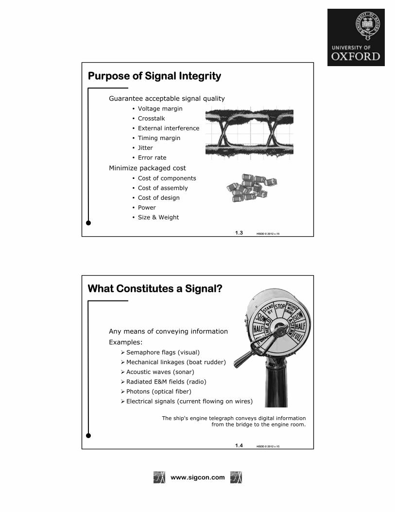
Purpose of Signal Integrity
Guarantee acceptable signal quality
Voltage margin
Crosstalk
External interference
Timing margin
Jitter
Error rate
Minimize packaged cost
Cost of components
Cost of assembly
Cost of design
Power
Size & Weight
1.4 HSDD © 2012 v.15
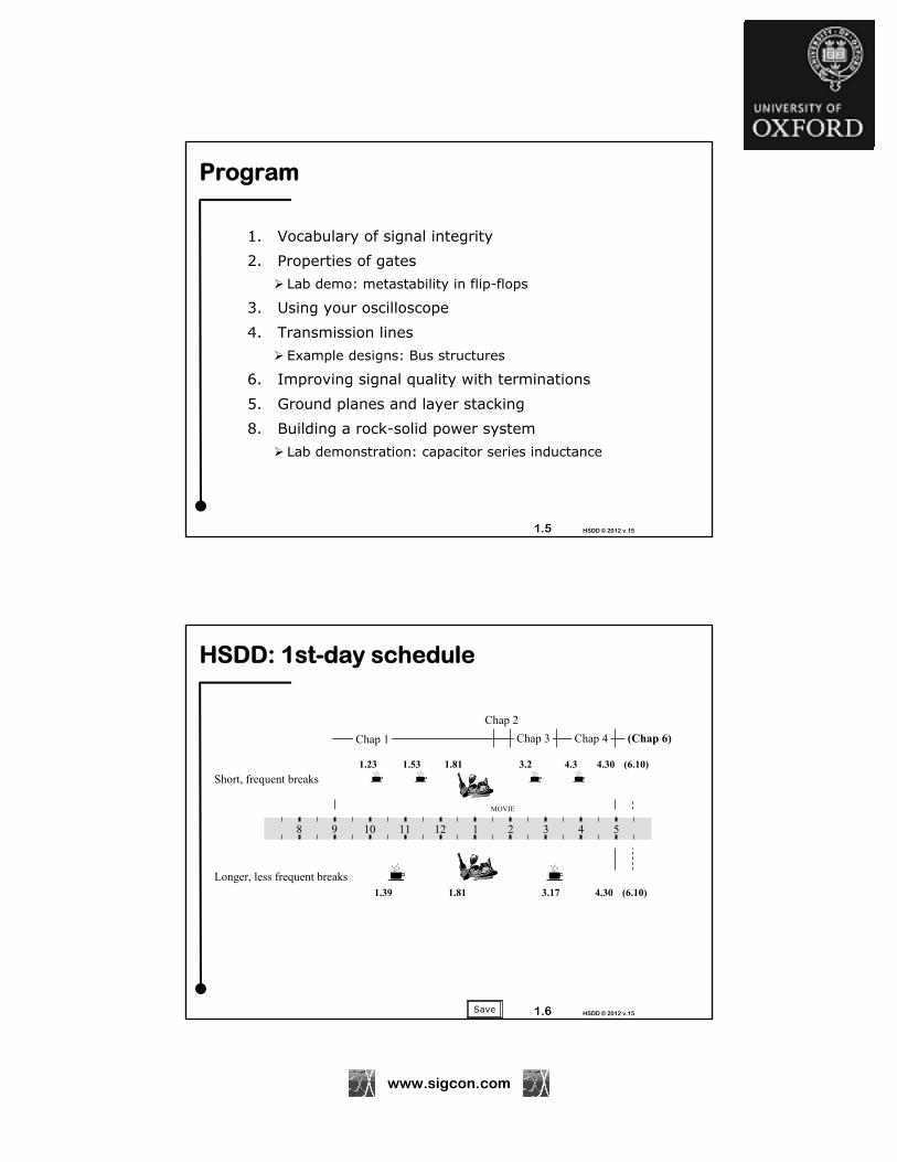
What Constitutes a Signal?
Any means of conveying information
Examples:
Semaphore flags (visual)
Mechanical linkages (boat rudder)
Acoustic waves (sonar)
Radiated E&M fields (radio)
Photons (optical fiber)
Electrical signals (current flowing on wires)
The ship's engine telegraph conveys digital information from the bridge to the engine room.
www.sigcon.com
1.5 HSDD © 2012 v.15
Program
1. Vocabulary of signal integrity
2. Properties of gates
Lab demo: metastability in flip-flops
3. Using your oscilloscope
4. Transmission lines
Example designs: Bus structures
6. Improving signal quality with terminations
5. Ground planes and layer stacking
8. Building a rock-solid power system
Lab demonstration: capacitor series inductance
1.6 HSDD © 2012 v.15
HSDD: 1st-day schedule
Save
8 9 10 11 12 1 2 3 4 5
Short, frequent breaks
Longer, less frequent breaks
Chap 1
Chap 2
Chap 3 Chap 4
1.23 1.53 1.81 3.2 4.3 4.30 (6.10)
1.39 1.81 3.17 4.30 (6.10)
(Chap 6)
MOVIE
www.sigcon.com
1.7 HSDD © 2012 v.15
HSDD: 2nd-day schedule
Save
8 9 10 11 12 1 2 3 4 5
Chap 6 Chap 5 Chap 8
6.24 5.4
6.41 5.4
Short, frequent breaks
Longer, less frequent breaks
EVALS | MOVIE
6.1
6.1
5.32 8.3 8.26
5.46 8.26
Freeform discussion complete
6.42
1.8 HSDD © 2012 v.15
HSDD: 2nd-day schedule (early release)
Save
8 9 10 11 12 1 2 3 4 5
Chap 5 Chap 6 Chap 12
6.41 6.52 5.17
6.42 5.17
Short, frequent breaks
Longer, less frequent breaks5.54 8.26
MOVIEEVALS
5.54 8.266.11
6.11
Freeform discussion complete

www.sigcon.com
1.9 HSDD © 2012 v.15
Questions?
I encourage questions. That is why I am here.
Please raise your hand and I’ll acknowledge that I’ve seen you. It may take me a minute, but I’ll get back to you when I get to a good stopping-point.
1.10 HSDD © 2012 v.15
Please Silence Cell Phones and Pagers
If you must take a call, please do so outside the room.
www.sigcon.com
1.11 HSDD © 2012 v.15
Chapter 1: Vocabulary of Signal Integrity
Circuit Elements
Parasitic Series Inductance
Parasitic Shunt Capacitance
Frequency and Time
Spectral content of digital signals
Propagation delay
Lumped versus distributed systems
Crosstalk effects
Mutual inductance
Mutual capacitance
1.12 HSDD © 2012 v.15
Your Schematic Is Lying
It shows only the intended flow of signal power.
It masks details crucial to the operation of unintentional signal pathways vital to your understanding of high-speed signal performance, crosstalk and EMI.
Two main rules govern unintentional signal flow.

www.sigcon.com
1.13 HSDD © 2012 v.15
Rule 1: Currents Form Loops
Source
Ground
Signal
Return
Load
50-
Current follows an obvious path in this
simple circuit.
Source
Ground
1.14 HSDD © 2012 v.15
Currents form loops in circuits of any complexity.
www.sigcon.com
1.15 HSDD © 2012 v.15
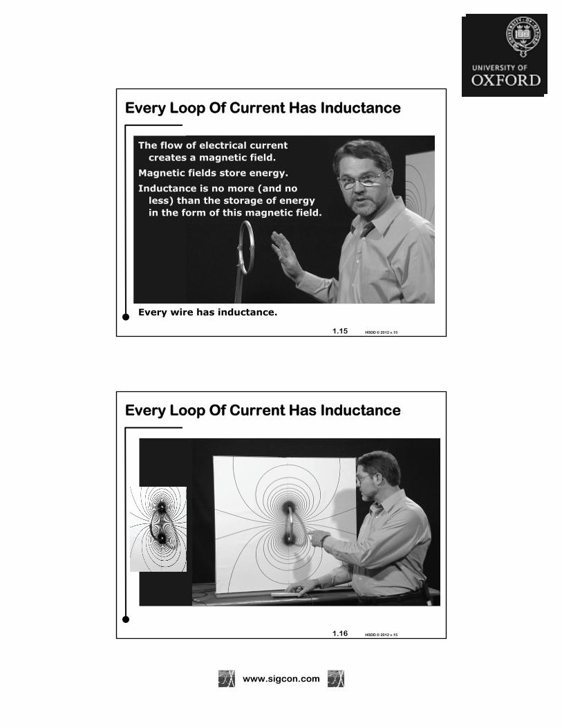
The flow of electrical current creates a magnetic field.
Magnetic fields store energy.
Inductance is no more (and no less) than the storage of energy in the form of this magnetic field.
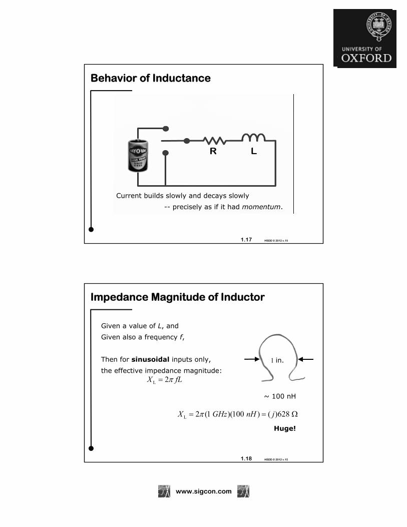
Every Loop Of Current Has Inductance
Every wire has inductance.
1.16 HSDD © 2012 v.15
Every Loop Of Current Has Inductance
www.sigcon.com
1.17 HSDD © 2012 v.15
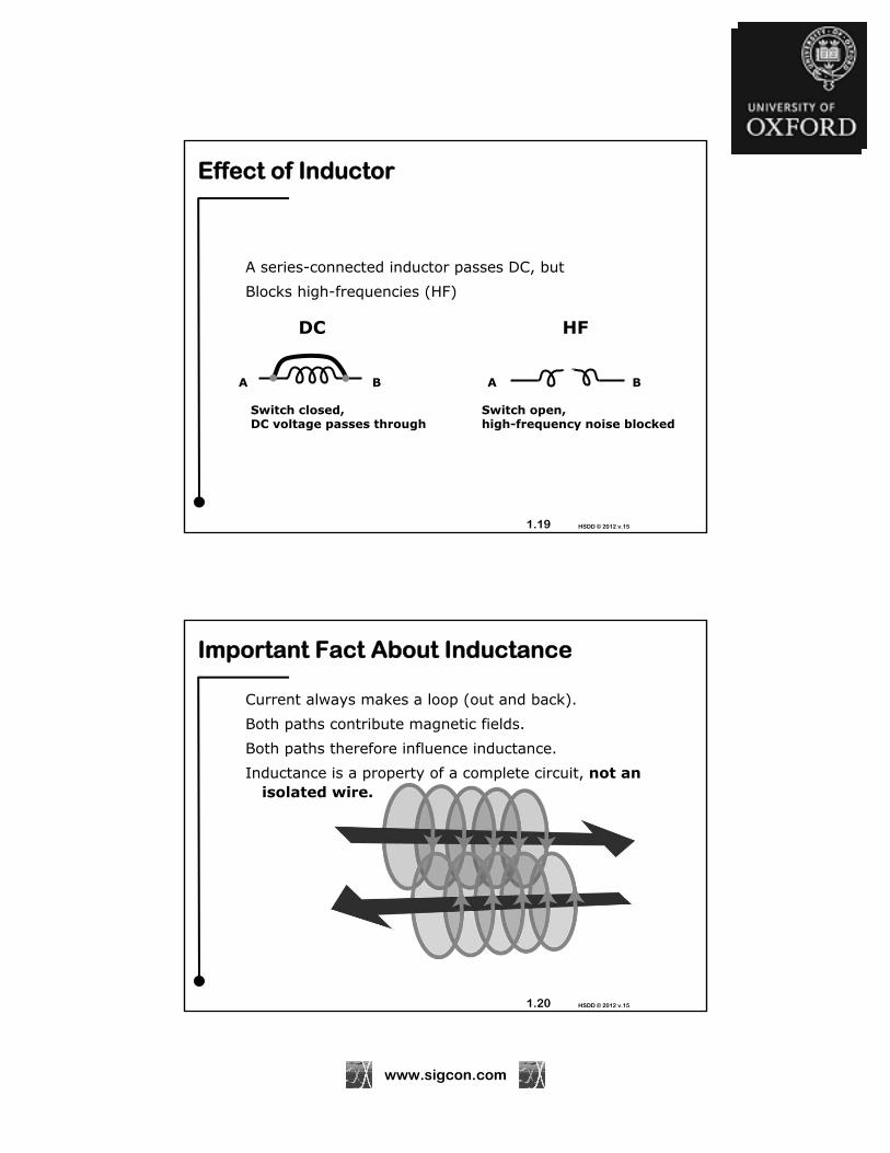
Behavior of Inductance
Current builds slowly and decays slowly
-- precisely as if it had momentum.
1.18 HSDD © 2012 v.15
Impedance Magnitude of Inductor
Given a value of L, and
Given also a frequency f,
Then for sinusoidal inputs only,
the effective impedance magnitude:
L 2X fL
1 in.
~ 100 nH
L 2 (1 )(100 ) ( )628 X GHz nH j
Huge!
www.sigcon.com
1.19 HSDD © 2012 v.15
Effect of Inductor
A series-connected inductor passes DC, but
Blocks high-frequencies (HF)
DC
Switch closed,DC voltage passes through
HF
Switch open,high-frequency noise blocked
A B A B
1.20 HSDD © 2012 v.15
Important Fact About Inductance
Current always makes a loop (out and back).
Both paths contribute magnetic fields.
Both paths therefore influence inductance.
Inductance is a property of a complete circuit, not an isolated wire.

www.sigcon.com
1.21 HSDD © 2012 v.15
A
B
Rule 2: Proximate ConductorsShare Capacitance
Any two conductors share an electric field.
Through this field unintentional currents flow.
The coupling acts like a shunt capacitance
1.22 HSDD © 2012 v.15
How Capacitors Behave
Turn the switch ON, …and current surges to fill the capacitor.
Turn the switch OFF,…and it just as quickly surges out.

www.sigcon.com
1.23 HSDD © 2012 v.15
Impedance Magnitude of Capacitor
Given a value of C, and
Given also a frequency f,
Then for sinusoidal inputs only,
the effective impedance magnitude:
C
1
2X
fC
C
1( )160
2 (1 )(1 )X j
GHz pF
Significant.
1 pF
1.24 HSDD © 2012 v.15
Effect of Capacitor
The capacitor blocks DC, but
Passes high-frequencies (HF)
DC
Switch open,no current
HF
Switch closed,direct connect
A
B
A
B

www.sigcon.com
1.25 HSDD © 2012 v.15
Approximate Values of Capacitance
Capacitance scales with size
Bigger objects have more capacitance
Capacitance varies inversely with spacing
Closer –> more capacitance
Further away –> less
h=0.01 in.
C=100 pF/(square in.)
(r=4.3)
C=3 pF/in.
Z0 = 50 ohmTDELAY= 150 ps/in.(microstrip r=4.3)
R0.2249 pFA
Ch
A
DELAY
0
pF/in. (assumes in ps/in.)T
C TZ
1.26 HSDD © 2012 v.15blank SaveExplore
www.sigcon.com
1.27 HSDD © 2012 v.15
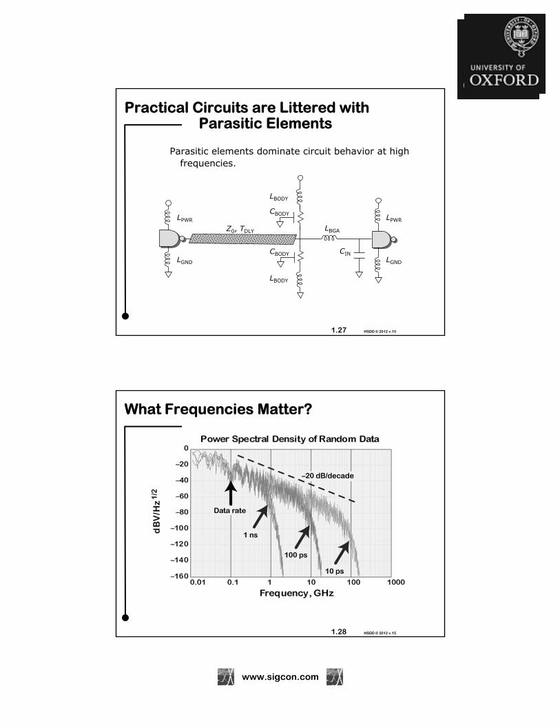
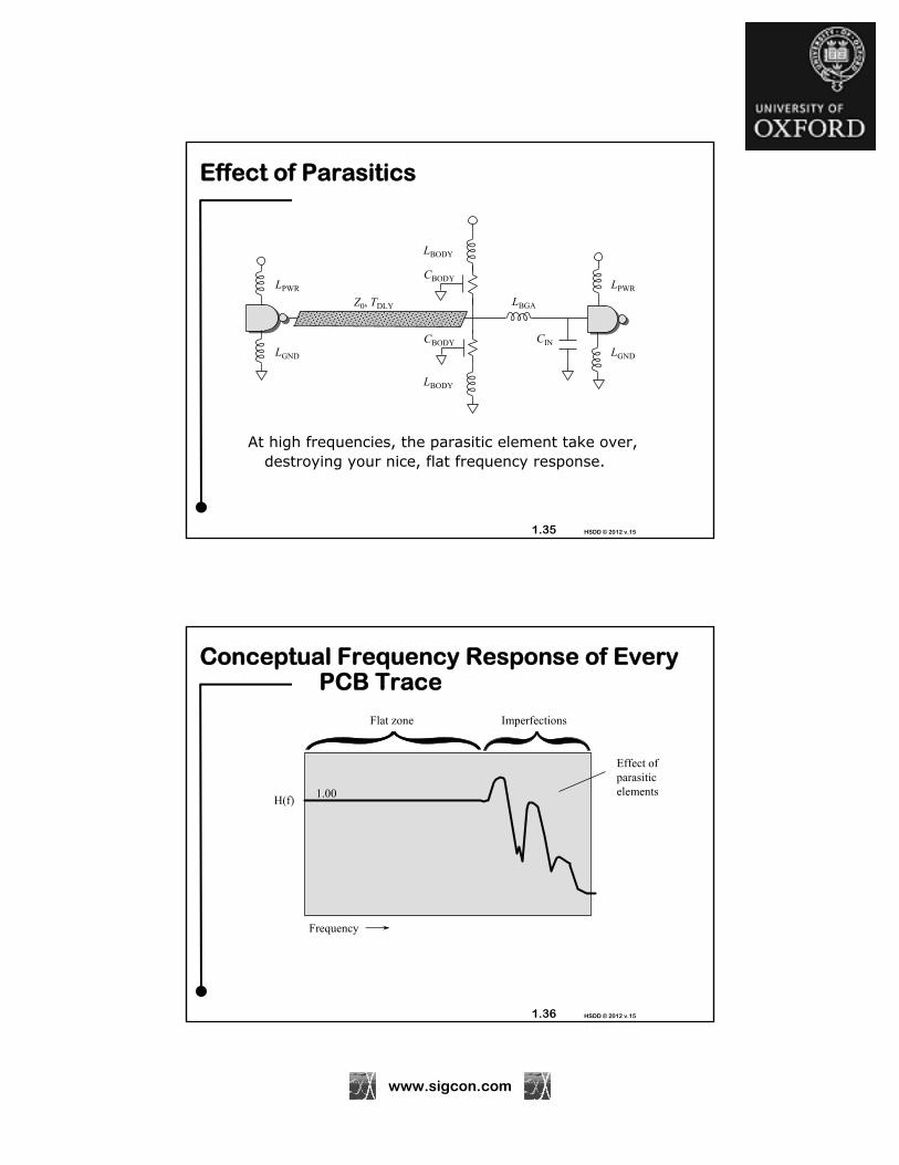
Practical Circuits are Littered with Parasitic Elements
Parasitic elements dominate circuit behavior at high frequencies.
CIN
LBGA
CBODY
CBODY
LBODY
LBODY
LPWR
LGND
LPWR
LGND
Z0, TDLY
1.28 HSDD © 2012 v.15
What Frequencies Matter?

www.sigcon.com
1.29 HSDD © 2012 v.15
Data Band
1.30 HSDD © 2012 v.15
Baud Interval Band (Rectangle = Step)
www.sigcon.com
1.31 HSDD © 2012 v.15
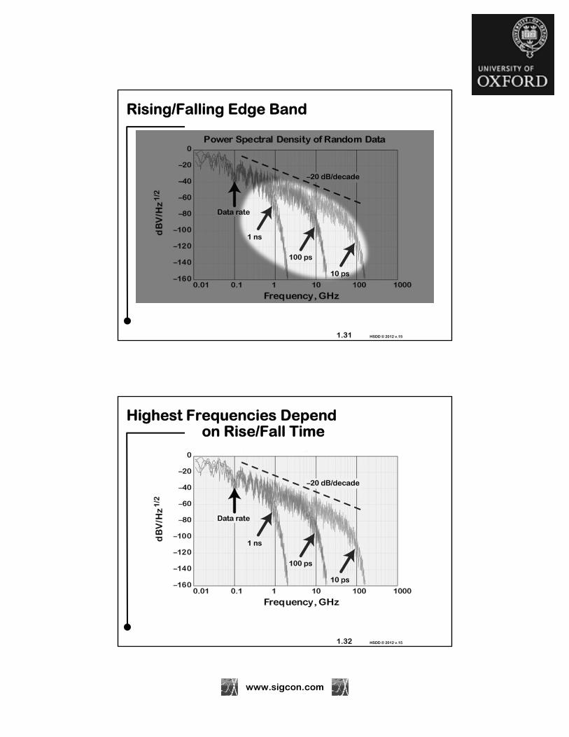
Rising/Falling Edge Band
1.32 HSDD © 2012 v.15
Highest Frequencies Depend on Rise/Fall Time

www.sigcon.com
1.33 HSDD © 2012 v.15
Frequencies That Matter for Digital Design
From DC up to the Knee Frequency
Knee frequency is a function of rise/fall time, not repetition rate
Frequency associated with incident wave Step-edge rise time
1-nS 500 MHz
KNEER
0.5F
T
FKNEE forms a crude, but useful, translation between the time and frequency domains.
1/4-nS 2000 MHz1/2-nS 1000 MHz
1.34 HSDD © 2012 v.15
Meaning of "Frequency Response"
Replace the driver with a sine-wave source having the same output impedance.
Measure the amplitude of the received signal y(t) as a function of frequency.
– x(t)+
y(t)+
–
"Frequency response" is the ratio of output magnitude to input
magnitude.
www.sigcon.com
1.35 HSDD © 2012 v.15
Effect of Parasitics
At high frequencies, the parasitic element take over, destroying your nice, flat frequency response.
CIN
LBGA
CBODY
CBODY
LBODY
LBODY
LPWR
LGND
LPWR
LGND
Z0, TDLY
1.36 HSDD © 2012 v.15
Conceptual Frequency Response of Every PCB Trace
H(f)1.00
Frequency
Flat zone Imperfections
Effect of parasitic elements

www.sigcon.com
1.37 HSDD © 2012 v.15
Relation of Knee Frequency to Circuit Performance
H(f)1.00
FKNEE
When the knee frequency is low, imperfections above FKNEE don’t matter
Frequency
1.38 HSDD © 2012 v.15
H(f)1.00
Frequency
Effect of Shrinking Rise/Fall Time
Faster circuits move FKNEE higher, exposing imperfections in the digital pathway
Constantly improving IC processes make circuits faster every year.
If your layout doesn't change, here's what happens:

www.sigcon.com
1.39 HSDD © 2012 v.15
Points to Remember
The response of a circuit at high frequencies affects its processing of short time events.
The response of a circuit at low frequencies affects its processing of long-term events
The important energy in digital pulses concentrates at or below the knee frequency.
To ensure good signal quality, digital circuits need a flat frequency response up to and including FKNEE.
The behavior of a digital circuit above FKNEE has little effect on signal quality.
FKNEE is a crude, but useful, translation between the time and frequency domains.
1.40 HSDD © 2012 v.15
International Technology Roadmap for Semiconductors (ITRS)
The International Technology Roadmap for Semiconductors (ITRS) is an assessment of the semiconductor technology requirements. The objective of the ITRS is to ensure advancements in the performance of integrated circuits. This assessment, called road-mapping, is a cooperative effort of the global industry manufacturers and suppliers, government organizations, consortia, and universities.
The ITRS identifies the technological challenges and needs facing the semiconductor industry over the next 15 years. It is sponsored by the Semiconductor Industry Association (SIA), the European Electronic Component Association (EECA), the Japan Electronics & Information Technology Industries Association (JEITA), the Korean Semiconductor Industry Association (KSIA), and Taiwan Semiconductor Industry Association (TSIA) .
International SEMATECH is the global communication center for this activity.
www.sigcon.com
1.41 HSDD © 2012 v.15
2011 Jan. update
International Technology Roadmap for Semiconductors
Dynamic RAM (Production)
High-perf. Microprocessor ASIC
Year ½ pitch, nm Chip size, mm2
Gbits per chip
Chip size, mm2
Billions of transistors
per chip
Chip-to-board bus (diff),
GHz
Wiring levels (max)
Total pins/balls
[1]
2011 40 49 4 260 4.4 12 12 5100
2013 32 31 4 260 8.8 17 13 5600
2016 22 31 8 260 17.7 34.9 13 6500
2019 16 31 16 260 35.4 50.7
14 7500
2022 11 31 32 260 70.8 67.5 15 8700
NOTE [1]—50% I/O, 50% Pwr&Gnd
www.itrs.net
1.42 HSDD © 2012 v.15
Propagation Delay in Various Media
Air (radio waves) 85 1.0
Coax cable (75% velocity) 113 1.8
Coax cable (66% velocity) 129 2.3
FR-4 PCB, outer trace 142-172 2.8-4.1 (effective)
FR-4 PCB, inner trace 172 4.1
Alumina PCB, inner trace 240-270 8.0-10.0
Medium Delay Dielectricps/in Constant r
r84.725 ps/in.DelayPerInch
2
r 84.725DelayPerInch (1 ) in./psv DelayPerInch

www.sigcon.com
1.43 HSDD © 2012 v.15
Example of Mixed Dielectric
Foaming the dielectric (adding air bubbles) reduces the effective electric permittivity.
Decreased delay
Increased speed
Less loss
Coaxial cables
Solid polyethylene
dielectric
Foamed polyethylene
dielectric
66% C 75% C
1.44 HSDD © 2012 v.15
Dielectric Properties of PCB Traces
Effective relative permittivity of microstrip lies between that of FR-4 and air
Microstrip traces go faster than striplines
Electric field exists partly in air, partly
in dielectric
Field is completely contained within
the dielectric
FR-4 dielectricr = 4.1
Reference plane(any DC voltage)
Reference plane(any DC voltage)
Microstrip
Stripline

www.sigcon.com
1.45 HSDD © 2012 v.15
Outer-Layer PCB Traces Are Faster
Signal arrives here first
Top layer
Bottom layer
Microstrip layer
Stripline layer
FR-4, r = 4.1
Traces have equal lengths.
1.46 HSDD © 2012 v.15
Points to Remember
• Propagation delay varies in proportion to the square root of the dielectric constant.
• The propagation delay of signals traveling in air equals 85 ps/in.
• Outer-layer pcb traces convey signals faster than inner-layer traces.

www.sigcon.com
1.47 HSDD © 2012 v.15
Distributed vs. Lumped Systems
Compact system
System delay << Rise/fall time
Easy to analyze using lumped-element assumptions
Characterized by simple harmonic motion
Lumped
Large, complicated system
System Delay >> Rise/fall time
Difficult distributed analysis required
Characterized by distributed delay and reflections
Distributed
1.48 HSDD © 2012 v.15
Critical RatiotD (System delay)
T10-90% (Rise/fall time)
Lumped
Distributed
Very small
1/6
1/3
Larger than 1/2
Lumped-element models accurate to 20%
Lumped-element models accurate to 2%
System reacts coherently; no model needed
System reacts in highly distributed fashion; extensive modeling required
Behavior

www.sigcon.com
1.49 HSDD © 2012 v.15
Re-Write the Critical Ratio
Classify circuits according to the relation between rising edge length and circuit size.
tD vtD
Let tD represent one-way circuit propagation delay (ps)Let v represent the wave velocity (in/ps)
Physical length of circuit= =
= T10-90% v(velocity, in./ps)
length ofrising edge (in)
(rise time, ps)
T10-90% vT10-90% Length of rising edge
×
1.50 HSDD © 2012 v.15
Start with a Big System
Loss Budgeting for Xilinx RocketIO, 2004

www.sigcon.com
1.51 HSDD © 2012 v.15
Rising Edge in Motion
1.52 HSDD © 2012 v.15
Edge is Much Larger than Capacitor

www.sigcon.com
1.53 HSDD © 2012 v.15
How Will It Compare to the Connector?
1.54 HSDD © 2012 v.15
Lumped-Element Assumption:"π " Model of Transmission Line
Circuitdimensions
<6
Totally equivalent circuits for 1-nS
risetime
T10-90% = 1 ns
1-in. trace10Load
L = delayZ0
C = (delay/Z0)
10
Load
LT10-90% = 1 ns "π" model
Applies when:
= 6 in.Z0 = 65 ohmdelay = 1/6 ns
½C ½C
www.sigcon.com
1.55 HSDD © 2012 v.15
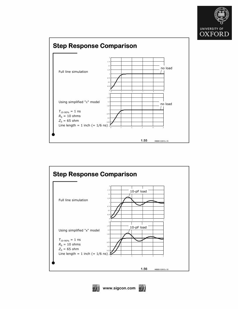
Step Response Comparison
T10-90% = 1 nsRS = 10 ohmsZ0 = 65 ohmLine length = 1 inch (= 1/6 ns)
Full line simulation
Using simplified "" model
0 1 2 3 4 50
0.25
0.5
0.75
1
1.25
1.5
1.75
2
0 1 2 3 4 50
0.25
0.5
0.75
1
1.25
1.5
1.75
2
no load
no load
1.56 HSDD © 2012 v.15
0 1 2 3 4 50
0.25
0.5
0.75
1
1.25
1.5
1.75
2
0 1 2 3 4 50
0.25
0.5
0.75
1
1.25
1.5
1.75
2
Step Response Comparison
T10-90% = 1 nsRS = 10 ohmsZ0 = 65 ohmLine length = 1 inch (= 1/6 ns)
Full line simulation
Using simplified "π" model10-pF load
10-pF load

www.sigcon.com
1.57 HSDD © 2012 v.15
Tricky Fact About the "π" Model
As long as you follow the rule: (tD/T10-90% ) < 1/6 ,
The capacitive impedance exceeds the inductive impedance for all frequencies up to the knee frequency.
Hint: into the ratio of (1/2fC)/(2fL), substitute the formulas for Land C given previously and the expression 2T10-90% for 1/f.
(1/2fC)/2fL
= (1/f)2 / (42LC)
= (2T10-90%)2 /[(42)(delayZ0)(delay/Z0)]
= (T10-90% /delay)2 / 2
> 62 /2
> 3.647
Ratio of impedances XC/XL
Combine like terms
Substitute for f, L, and C
Express T/delay ratio in numerator
The rule says T10-90%/tD > 6Ratio by which the capacitive
impedance exceeds the inductive impedance
1.58 HSDD © 2012 v.15
Uses for The "π" Model"π" model of short line, grounded at far end
These impedances are too large to matter...
Input
"π" model of short line, open at far end
This impedance is too small to matter...
Input
L
L
½C ½C
½C ½C
Net result
Net result
…looks like an inductor to ground
…looks like a lumped capacitive load
L
C
L = delay*Z0
C = (delay/Z0)
www.sigcon.com
1.59 HSDD © 2012 v.15
Points to Remember
Rise time relates to physical dimensions:
Circuits smaller than /6 behave as lumped circuits, for which the "π" model may be used
= T10-90% v(velocity, in./ps)(rise time, ps)
×
1.60 HSDD © 2012 v.15
Taxonomy of Component Behavior at High Frequencies
Capacitance
Draws a surge of drive current, and causes reflections on long lines
Inductance
Causes ground bounce and power supply noise
Mutual capacitance
Causes crosstalk between high impedance circuits
Mutual inductance
Causes crosstalk in connectors and in bad layouts
These concepts provide a rich language for describing and understanding the behavior of digital
circuit elements at high speeds.

www.sigcon.com
1.61 HSDD © 2012 v.15
Classify Reactance With aStep Response Test
Device under testshunts the stepsource
Output impedanceof step source
x(t)Step
source
+
-
RS
+
-Z
I(t)
Step responsey(t)
1.62 HSDD © 2012 v.15
Step Response of Various Reactances
Resistor
Initial step to fraction of open circuit voltage
Stays flat
Capacitor
No initial step
Ramps up to full output
Inductor
Full size initial step
Decays to zero
RL
RS
RS
RS
C
y(t)
y(t)
Same rise time as source
Voltage approachesfull output
x(t) RL
RL + RS
Holds flat at fixed voltage:
Initial stepis full size Voltage decays
to zero
Same rise time as source
0-63% = RSC
100-37% = L/RS
y(t)
y(t)
y(t)
x(t)
x(t)
L
y(t)x(t)
www.sigcon.com
1.63 HSDD © 2012 v.15
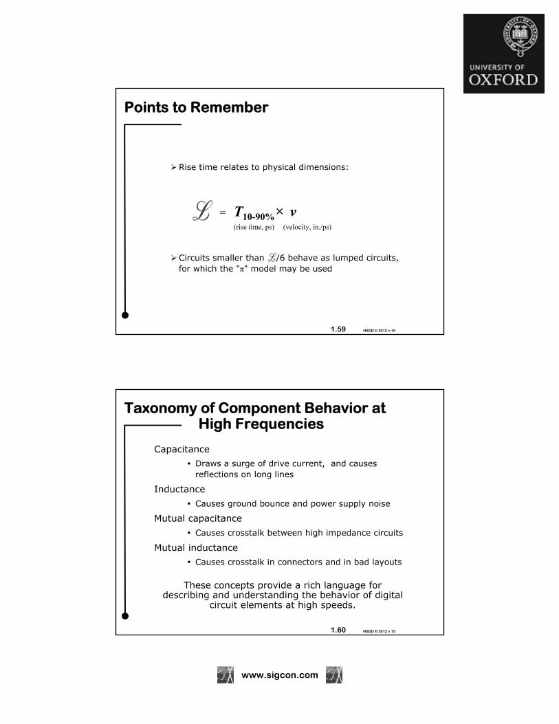
Resistive Step Response: Leaves T10-90% Unchanged
y(t)
10
Signal rises to only 90% of unloaded response
(Same in all cases)
90% of this signal’s own final value
x(t)
RL =
y(t)
t
RL = 100
RL = 10
RL = 1
T10-90%
RL
1.64 HSDD © 2012 v.15
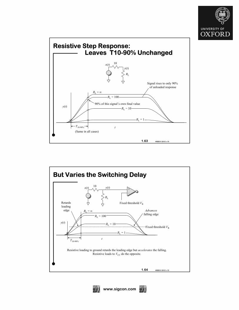
But Varies the Switching Delay
RL =
RL = 100
RL = 10
RL = 1
y(t)
tT10-90%
Fixed threshold VR
y(t)10
Fixed threshold VR
+-
Resistive loading to ground retards the leading edge but accelerates the falling.Resistive loads to VCC do the opposite.
Retards leading
edge Advancesfalling edge
x(t)
RL

www.sigcon.com
1.65 HSDD © 2012 v.15
Points to Remember
A resistive step response leaves T10-90% unchanged, but varies the switching delay.
A capacitive step response rises.
An inductive step response decays.
1.66 HSDD © 2012 v.15
Mutual Capacitance
End View of twoadjacent terminating resistors
RA
0.1 in.
BR
No copper on circuit sideof printed circuit board (PCB)
0.063-in.-thick epoxy FR-4 PCB
Solid ground plane on solderside of PCB
Wherever there are two circuits, there is mutual capacitance.
About 0.4 pF
www.sigcon.com
1.67 HSDD © 2012 v.15
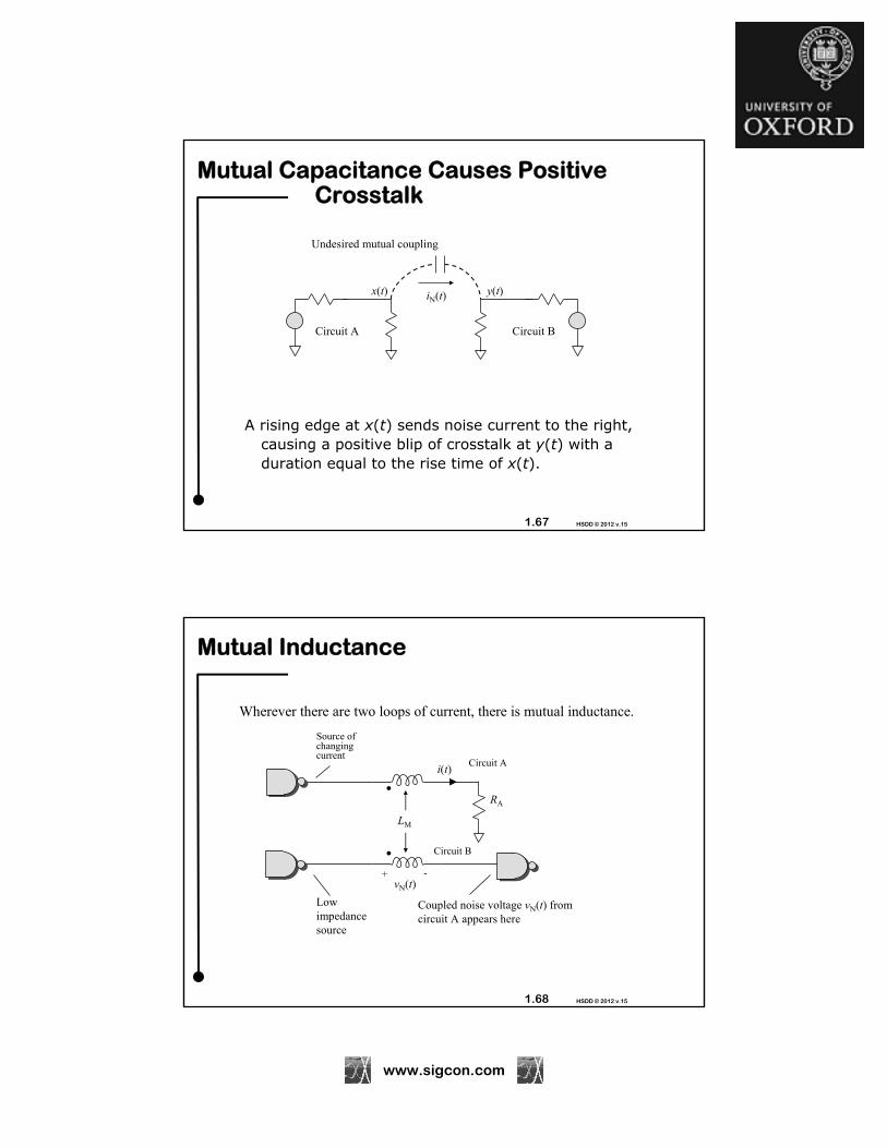
Mutual Capacitance Causes Positive Crosstalk
A rising edge at x(t) sends noise current to the right, causing a positive blip of crosstalk at y(t) with a duration equal to the rise time of x(t).
Circuit A Circuit B
Undesired mutual coupling
x(t) y(t)iN(t)
1.68 HSDD © 2012 v.15
Mutual Inductance
Wherever there are two loops of current, there is mutual inductance.
vN(t)
Lowimpedancesource
+
LM
Source ofchangingcurrent
Coupled noise voltage vN(t) from circuit A appears here
Circuit B
-
i(t)
RA
Circuit A
www.sigcon.com
1.69 HSDD © 2012 v.15
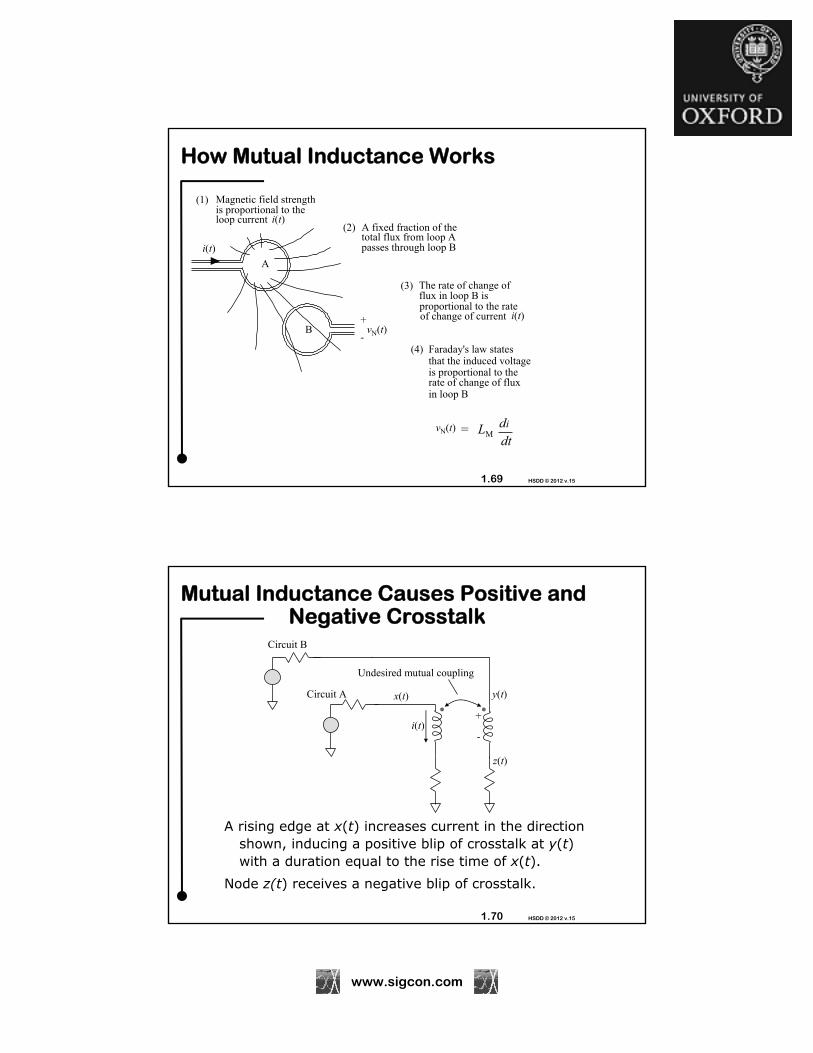
How Mutual Inductance Works
Faraday's law states that the induced voltageis proportional to therate of change of fluxin loop B
(4)
Magnetic field strengthis proportional to theloop current
(1)
i(t)A fixed fraction of thetotal flux from loop A passes through loop B
(2)
The rate of change offlux in loop B is proportional to the rateof change of current
(3)
i(t)
i(t)
B
A
vN(t)-
+
vN(t) = di
dtLM
1.70 HSDD © 2012 v.15
-
+
Mutual Inductance Causes Positive and Negative Crosstalk
A rising edge at x(t) increases current in the direction shown, inducing a positive blip of crosstalk at y(t) with a duration equal to the rise time of x(t).
Node z(t) receives a negative blip of crosstalk.
Circuit A
Circuit B
x(t) y(t)
i(t)
z(t)
Undesired mutual coupling

www.sigcon.com
1.71 HSDD © 2012 v.15
Practical Measurement ofMutual Coupling
From pulsegenerator
IN
OUT
RB
50
To scope
RA
50
Note: Resistors are eachgrounded on one end
We expect both inductive and capacitive coupling to occur
1.72 HSDD © 2012 v.15
Mutual Coupling of Two 1/4-W Resistors
FIG 1.22
Amplitude (3)91 mV
Area (3)79.96 pVs
1 V
20 mV
20 mV
(1)
(2)
(3)
5 nS/div
500 pS/div

www.sigcon.com
1.73 HSDD © 2012 v.15
Mutual Coupling Measurement Againwith Reversed Sense Probe
From pulsegenerator
IN
OUTRB
50
To scope
RA
50
When reversing the sense probe:• Inductive coupling flips polarity• Capacitive coupling retains same polarityThis is how we can tell the difference
Note: Resistors are eachgrounded on one end
1.74 HSDD © 2012 v.15
Mutual Coupling of Two 1/4-W Resistors
FIG 1.23
Amplitude (3)70 mV
Area (3)58.91 pVs
1 V
20 mV
20 mV
(1)
(2)
(3)
5 nS/div
500 pS/div

www.sigcon.com
1.75 HSDD © 2012 v.15
Comparison of Inductive and Capacitive Crosstalk
In digital crosstalk problems, when a low-impedance circuit is exposed to the air through a package pin, connector, or
component body, look first for inductive crosstalk.
Higher impedance circuits (like on-chip nets)experience more capacitive crosstalk.
C-crosstalk 0.4 %
L-crosstalk 3.3 %Typical ratio for50-Ω circuits
(FIG. 1.22 or 1.23)
(Difference between FIG 1.22 and 1.23)
1.76 HSDD © 2012 v.15
Why I Care About the Difference Between Capacitive and Inductive Crosstalk
Aggressor
Victim
0
PCB
(Open-loop wiring)
Load 1
Load 2-
Y(t)+
Undesirable capacitive coupling goes from one signal wire to the other
www.sigcon.com
1.77 HSDD © 2012 v.15
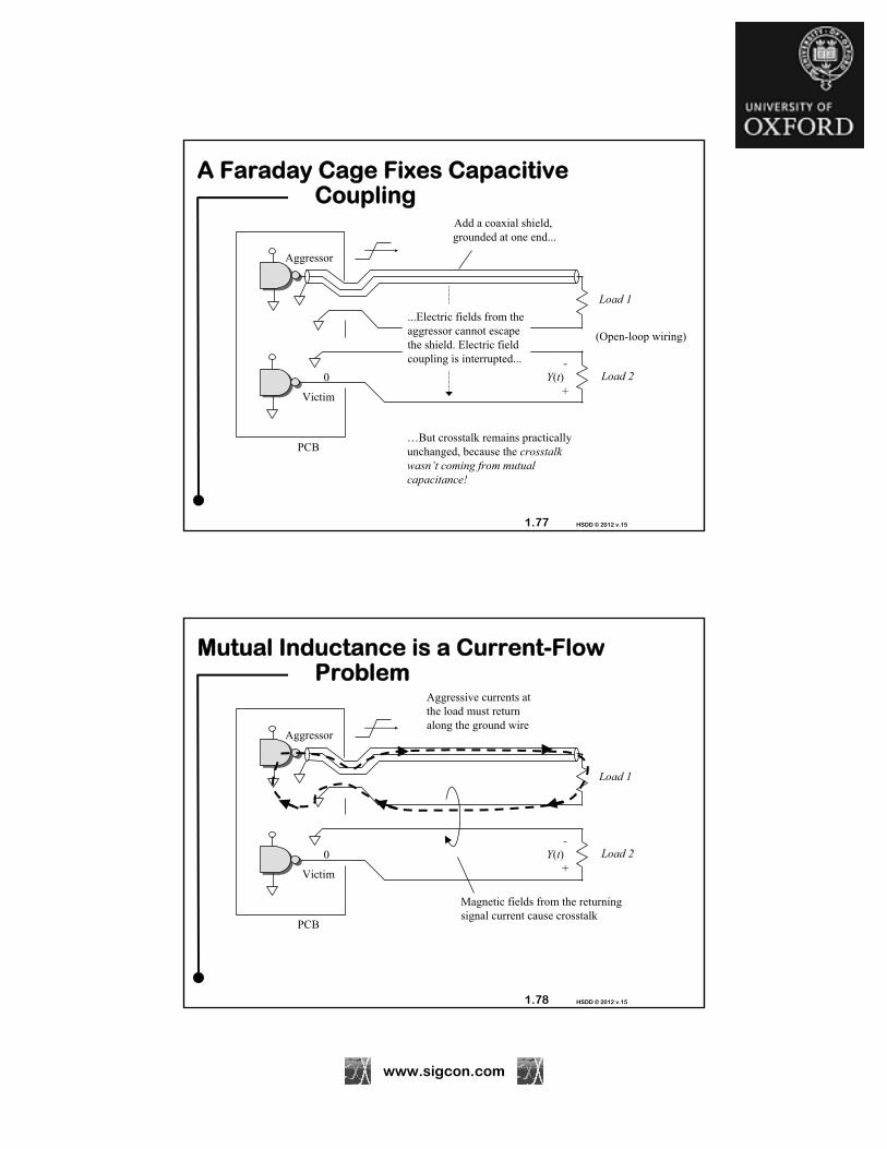
A Faraday Cage Fixes Capacitive Coupling
Aggressor
Victim
0
PCB
(Open-loop wiring)
Load 1
Load 2-
Y(t)+
...Electric fields from the aggressor cannot escape the shield. Electric field coupling is interrupted...
Add a coaxial shield, grounded at one end...
…But crosstalk remains practically unchanged, because the crosstalk wasn’t coming from mutual capacitance!
1.78 HSDD © 2012 v.15
Mutual Inductance is a Current-Flow Problem
Aggressor
Victim
0
PCB
Load 1
Load 2-
Y(t)+
Aggressive currents at the load must return along the ground wire
Magnetic fields from the returning signal current cause crosstalk
www.sigcon.com
1.79 HSDD © 2012 v.15
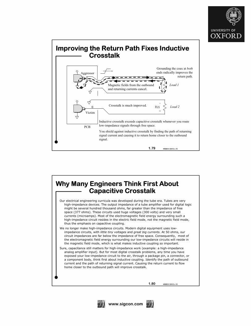
Improving the Return Path Fixes Inductive Crosstalk
Inductive crosstalk exceeds capacitive crosstalk whenever you route low-impedance signals through free space.
You shield against inductive crosstalk by finding the path of returning signal current and causing it to return home closer to the outbound signal.
Aggressor
Victim
0
PCB
Load 1
Load 2-
Y(t)+
Grounding the coax at bothends radically improves the
return path.
Magnetic fields from the outbound and returning currents cancel.
Crosstalk is much improved.
1.80 HSDD © 2012 v.15
Why Many Engineers Think First About Capacitive Crosstalk
Our electrical engineering curricula was developed during the tube era. Tubes are very high-impedance devices. The output impedance of a tube amplifier used for digital logic might be several hundred thousand ohms, far greater than the impedance of free space (377 ohms). These circuits used huge voltages (300 volts) and very small currents (microamps). Most of the electromagnetic field energy surrounding such a high-impedance circuit resides in the electric field mode, not the magnetic field mode, thus the emphasis on capacitive coupling.
We no longer make high-impedance circuits. Modern digital equipment uses low-impedance circuits, with little tiny voltages and great big currents. At 50 ohms, our circuit impedances are far below the impedance of free space. Consequently, most of the electromagnetic field energy surrounding our low-impedance circuits will reside in the magnetic field mode, which is what makes inductive coupling so important.
Sure, capacitance still matters for high-impedance work (example: a high-impedance analog amplifier input). But for most digital crosstalk problems, any time you have exposed your low-impedance circuit to the air, through a package pin, a connector, or a component body, think first about inductive coupling. Identify the path of outbound current and the path of returning signal current. Causing the return current to flow home closer to the outbound path will improve crosstalk.
www.sigcon.com
1.81 HSDD © 2012 v.15
Points to Remember
Mutual capacitance causes positive crosstalk with a duration equal to the rise time of the aggressive signal.
Mutual inductance can cause either positive or negative crosstalk, with a duration equal to the rise time of the aggressive signal.
Among high-speed, low impedance digital circuits, mutual inductance is often a worse problem than mutual capacitance.
1.82 HSDD © 2012 v.15
Path of Current
First movieon disk
Eleven minutes

www.sigcon.com
1.83 HSDD © 2012 v.15
Extra for Experts
My next course, Advanced High-Speed Signal Propagation,covers the following topics: Lossy transmission structures Pcb tracesDifferential connections Serial links S-parameters Equalizers ViasConnectorsClock routing, andClock jitter.
A brief excerpt from the course follows. This material is adapted from the book, High-Speed Signal Propagation: Advanced Black Magic.
1.84 HSDD © 2012 v.15
Skin Effect and Dielectric Loss Chart
107 108 109 1010
0.01
0.1
1
10
Dielectric loss in percent per inch
vs. dielectric loss tangent All traces are striplines
(microstrips have slightlyless loss)
Skin effect lossin percent per inchvs. trace width w.
All traces are loosely-coupled 100-ohm differential pairs.
w=.006 in.w=.012 in.
w=.024 in.
= .02 = .01 = .005
Frequency, Hz

www.sigcon.com
1.85 HSDD © 2012 v.15
Skin Effect and Dielectric Loss ExampleFibre Channel 1.06 Gb/s over 18 in. of FR-4
107 108 109 1010
0.01
0.1
1
10Composite loss (skin+dielectric) at maximum data
alternation rate is 1% per inch; Loss in 18 inches is 18%
For more accurate results use a 2-D field solver to computeskin loss and effective dielectricloss tangent
Trace loss, percent per inch
503 MHz = ½·1.06 Gb/s
Skin effect w=.012 in.
Dielectric loss tan. = .02

!!!"#$%&'("&')

www.sigcon.com
HSDD © 2012 v.15
Chapter 2: Properties of Gates
Ground bounce
IBIS (Supplemental)
2.2 HSDD © 2012 v.15
Voltage Margin Budget
VCC MIN
VOH
VIH
0V
VOL
VIL
VCC
DriverPackagedreceiver
Die thresholds(JEDEC 3.3V CMOS)
PowerSystem
Board-level ringing, crosstalk, ground shifts and other noise
Crosstalk (ground bounce) within package
Driver R[OUT]
–10%

www.sigcon.com
2.3 HSDD © 2012 v.15
What Is Ground Bounce?
Ground Bounce is also called
Simultaneously Switching Output Noise
SSO Noise
Packaging crosstalk
Ground bounce causes glitches in your logic inputs when the device outputs switch.
2.4 HSDD © 2012 v.15
SSO Test Setup
Observe noise on the victim circuit while transmitting multiple aggressive signals.
Victim crosstalk
Gnd
Scope
Gnd
Vcc
Victim stuck high (or low)
DC Block
BGA package
Z0=50
Z0=50
Multiple aggressors
J1
www.sigcon.com
2.5 HSDD © 2012 v.15
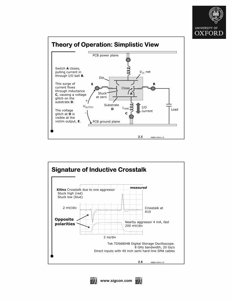
Theory of Operation: Simplistic View
B
A
E
I/Ocurrent
PCB ground plane
Load
VCC net
PCB power plane
Stuckat zero
Substrate
Die
DVGLITCH
+
–
Close
LGND
C
Switch A closes, pulling current in through I/O ball B.
This surge of current flows through inductance C, causing a voltage glitch on the substrate D.
The voltage glitch at D is visible at the victim output, E.
2.6 HSDD © 2012 v.15
Signature of Inductive Crosstalk
2 mV/div
2 ns/div
Xilinx Crosstalk due to one aggressorStuck high (red)Stuck low (blue)
Nearby aggressor 4 mA, fast200 mV/div
Tek TDS6804B Digital Storage Oscilloscope.8 GHz bandwidth, 20 Gs/s
Direct inputs with 40 inch semi hard-line SMA cables
measured
Crosstalk at A10
Opposite polarities
www.sigcon.com
2.7 HSDD © 2012 v.15
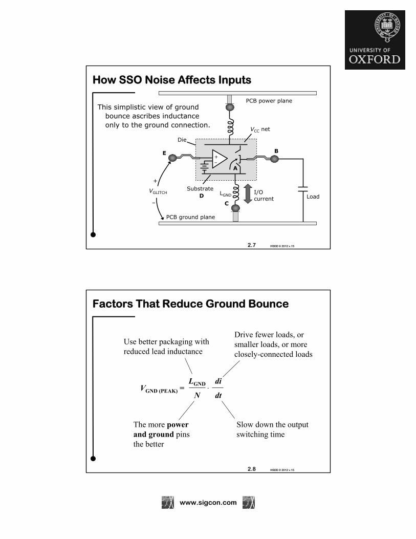
How SSO Noise Affects Inputs
This simplistic view of ground bounce ascribes inductance only to the ground connection.
B
A
E
PCB power plane
PCB ground plane
Load
VCC net
Substrate
Die
DVGLITCH
+
–
LGND
C
+–
I/Ocurrent
2.8 HSDD © 2012 v.15
Factors That Reduce Ground Bounce
VGND (PEAK) =LGND
N
di
dt
Slow down the output switching time
The more power and ground pins the better
Use better packaging with reduced lead inductance
Drive fewer loads, or smaller loads, or more closely-connected loads

www.sigcon.com
2.9 HSDD © 2012 v.15
A Well-dispersed Array of Pwr/Gnd Pins
TEST BOARD24 layers
110 mil thick3 I/O power regions
500 active I/O’s34x34 BGA
2.10 HSDD © 2012 v.15
Crosstalk Contributions Affecting A10
SC
Victim A-10 is back here on the first row5 mV
Crosstalk from individual neighbors
www.sigcon.com
2.11 HSDD © 2012 v.15
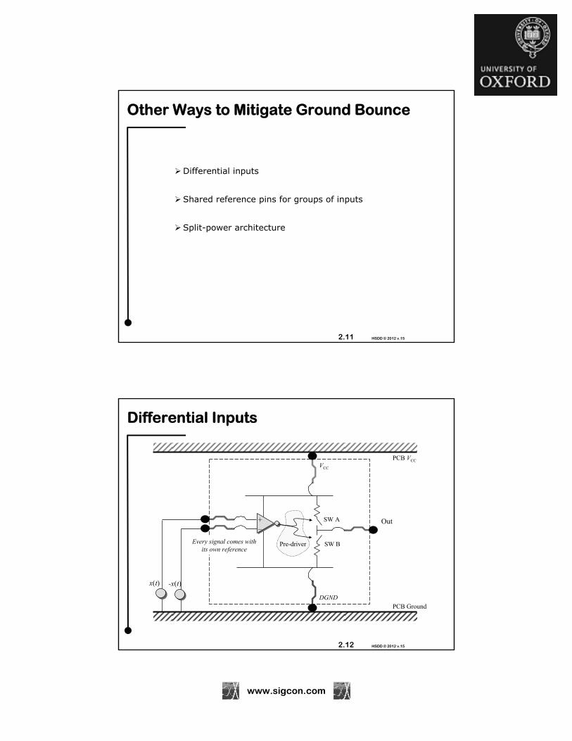
Other Ways to Mitigate Ground Bounce
Differential inputs
Shared reference pins for groups of inputs
Split-power architecture
2.12 HSDD © 2012 v.15
Differential Inputs
x(t)
SW B
SW A
VCC
Out+–
Pre-driver
PCB Ground
PCB VCC
DGND
-x(t)
Every signal comes with its own reference

www.sigcon.com
2.13 HSDD © 2012 v.15
Shared Reference
x3
SW B
SW A
VCC
Out
Pre-driver
PCB Ground
PCB VCC
DGND
ref
Groups of signals share one input
reference
+–
+–
+–
x1 x2
2.14 HSDD © 2012 v.15
Split-Power Architecture: Core Logic
x(t)
VR-
+
VCC1
+–
Pre-driver
PCB Ground
PCB VCC
AGND
Slide 2.22 overlay

www.sigcon.com
2.15 HSDD © 2012 v.15
Split-Power Architecture: I/O Ring
PCB Ground
PCB VCC
SW B
VCC2
SW A Out
DGND
Slide 2.22 overlay
2.16 HSDD © 2012 v.15
Split-Power Architecture: Core + I/O Ring
x(t)
VR-
+
VCC1
+–
Pre-driver
PCB Ground
PCB VCC
Out
VCC2
SW B
SW A
DGNDAGND
www.sigcon.com
2.17 HSDD © 2012 v.15
Points to Remember
Large I/O currents flow through your power and ground connections
These currents cause SSO (ground bounce and power bounce)
SSO noise can double-clock your flip flops
At high speeds, low-inductance packaging becomes crucial
Differential inputs conquer ground bounce
2.18 HSDD © 2012 v.15
Extra for Experts
Inside BGA Packages

www.sigcon.com
2.19 HSDD © 2012 v.15
Plastic Ball Grid Array (PBGA)
Adapted from John Lau, Ball Grid Array Technology, McGraw-Hill, 1995, ISBN 0-07-036608-X
Via for ground / signal
Gold wire Molding compound Die pad Plated copperconductor
Solder maskVia for
ground / thermalSolder ball
IC
Chip mounts face-up
B-T epoxysubstrate
2.20 HSDD © 2012 v.15
AMKOR Plastic Ball Grid Array (PBGA) with Solder-Bumped Flip Chip
Adapted from John Lau, Ball Grid Array Technology, McGraw-Hill, 1995, ISBN 0-07-036608-X
Underfillencapsulant
Signal/groundvia
Plated copper conductor
Solder mask
Solder ballThermal/ground viaB-T epoxy substrate
Solder mask
IC
Chip mounts face-down
www.sigcon.com
2.21 HSDD © 2012 v.15
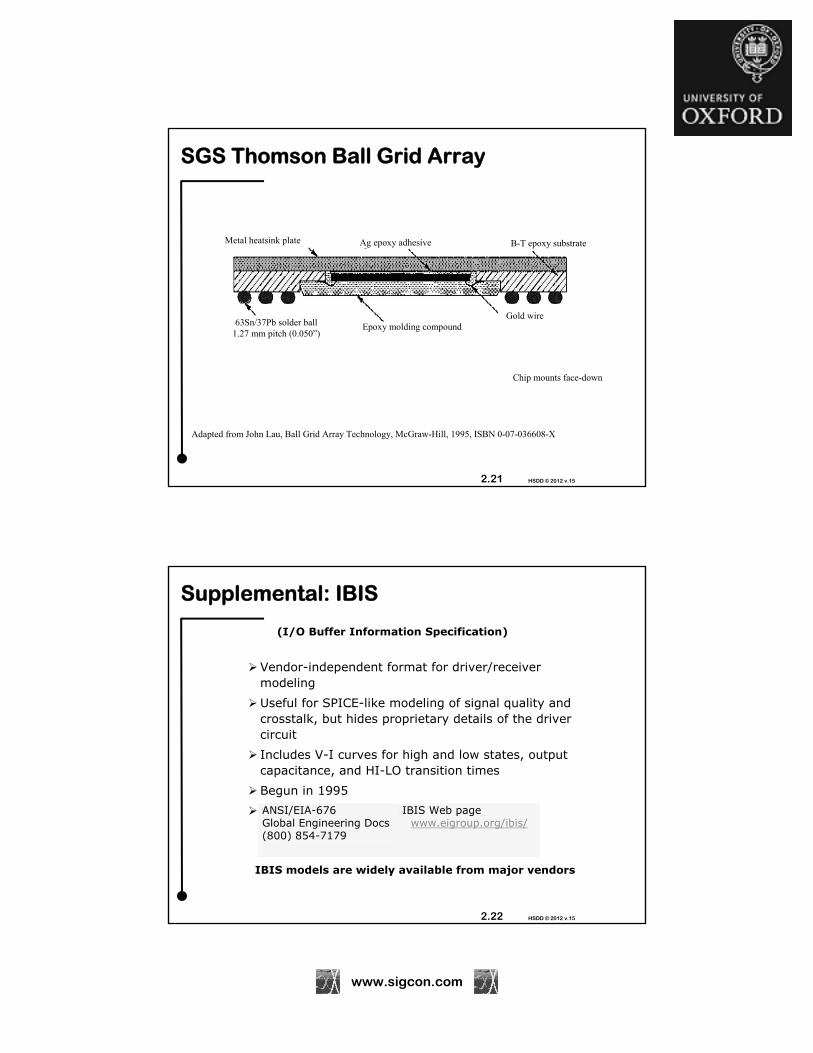
SGS Thomson Ball Grid Array
Adapted from John Lau, Ball Grid Array Technology, McGraw-Hill, 1995, ISBN 0-07-036608-X
Metal heatsink plate Ag epoxy adhesive B-T epoxy substrate
63Sn/37Pb solder ball1.27 mm pitch (0.050”)
Epoxy molding compoundGold wire
IC
Chip mounts face-down
2.22 HSDD © 2012 v.15
Supplemental: IBIS
Vendor-independent format for driver/receiver modeling
Useful for SPICE-like modeling of signal quality and crosstalk, but hides proprietary details of the driver circuit
Includes V-I curves for high and low states, output capacitance, and HI-LO transition times
Begun in 1995
Ver. 4.2 (ANSI/EIA-656-A) ratified 2006ANSI/EIA-676 Global Engineering Docs (800) 854-7179
IBIS Web page www.eigroup.org/ibis/
IBIS models are widely available from major vendors
(I/O Buffer Information Specification)

www.sigcon.com
2.23 HSDD © 2012 v.15
Component-centric Modeling
One component comprises of multiple I/O typesplaced on the component pins.
GND
A
A
A
B
C
C
C
VCC
B
B
B
B
B
7
1
2
3
4
5
6
8
14
13
12
11
10
9
2.24 HSDD © 2012 v.15
VccVcc
Basic IBIS Output Architecture
R_pkg
C_comp
L_pkg
C_pkg
PullupPulldown
ESD Package model

www.sigcon.com
2.25 HSDD © 2012 v.15
Meaning of V-I Curves
The V-I curve for a driver defines its static behavior.
= (VCC–VOH) / IOH
2.26 HSDD © 2012 v.15
IBIS Input Architecture
Vcc
R_pkg
C_comp
L_pkg
C_pkg
Die cap.ESDPackage model
RCV

www.sigcon.com
2.27 HSDD © 2012 v.15
Best Points About IBIS
The V-I curves measured under multiple load conditions are very useful (v2.2).
Use IBIS for ringing and board-level crosstalk simulation below 1 GHz.
It’s more of a specification than a behavioral model, which allows vendors to make multiple versions of chips that all conform to the specification.
IBIS accommodates hierarchical modeling of thousands of pins.
The models are human-readable, and human-fixable.
IBIS models run quickly.
2.28 HSDD © 2012 v.15
IBIS Limitations
Many vendors don’t provide models
Models provided are often missing sections, or wrong
Chips are not guaranteed to perform to the model
Non-linear aspects of ground bounce are not captured in the model; IBIS-based simulators tend to overestimate ground bounce (IBIS is working on this)
High-frequency behavior in complex packages is a very complex problem
Not as detailed a model as SPICE, but then you rarely see a SPICE model of a 600-pin chip.
Differential driver models are accurate only if you use the same common-mode loading conditions used during model generation.
Even with these limitations, IBIS is a great tool and well worth using.
Practical:
Technical:

www.sigcon.com
2.29 HSDD © 2012 v.15
Sharp Edges
Harish from UT Arlington writes: "I tried the following snippet in PSPICE and found oscillations in the output." Isn't this circuit too short to have such ringing??
Fig. 1
tD/T10-90% = 1/16
2.30 HSDD © 2012 v.15
Decompose the Signal
PWL edge = Gaussian edge + (PWL - Gaussian)

www.sigcon.com
2.31 HSDD © 2012 v.15
Frequency Response
2.32 HSDD © 2012 v.15
High-frequency Content in the PWL Edge Causes Visible Resonance
Simulate using a signal that "looks like" the signals in your actual system.

www.sigcon.com
2.33 HSDD © 2012 v.15
A 5th-order Gaussian Edge Generator
Anatol I. Zvrev, "Handbook of Filter Synthesis", John Wiley, 1967
1 ns10-90%
Controlled voltage source buffers output signal
2.34 HSDD © 2012 v.15
Points to Remember
IBIS is coming (ask your vendors for it).
For PCBs operating below 1 GHz most signal integrity simulation software available today can accurately calculate ringing and board-level crosstalk.

!!!"#$%&'("&')
www.sigcon.com
HSDD © 2012 v.15
Chapter 3: Using Your Oscilloscope
You can’t debug a problem that you can’t see.
Popular types of probes
Probe loading factor
Risetime and bandwidth
Sensitivity to the probe ground wire
Measuring your noise floor
Grounding a differential probe
3.2 HSDD © 2012 v.15
Popular Probes for High-Speed Digital Work
Low-capacitance active probe
Differential active probe
Resistive-input probe

www.sigcon.com
3.3 HSDD © 2012 v.15
FET-input probe
The FET amplifier acts as a buffer separating the input circuit from the cable effects
Uses the cable in a true 50-Ω transmission line mode - the cable can be any length
Tip gets warm due to power dissipation
Connector pinouts must be compatible with scope
Easily blown out by electrostatic discharge—wear a wrist strap!
FET-input amplifier ishidden in the tip
50-Ω terminatorat scope input
50-Ω coax cableTip
Ground
Equalizer andpower conditioningat end of cable
Power is carriedin the probe cable
Input capacitancetip-to-ground ranges from 2 to as littleas 1/6 pF
Bandwidths to 8 GHz
3.4 HSDD © 2012 v.15
Differential Active Probe
Very similar to single-ended FET probe.
Now with even higher bandwidth options at 250-300 ohms input impedance.
FET-input amplifier ishidden in the tip
Sig (+)Sig (-)
Ground(not used)
Equalizer andpower conditioningat end of cable
Input capacitanceon the order of 1-2 pFeach side to ground.
50-Ω coax cable
Power is carriedin the probe cable
+-

www.sigcon.com
3.5 HSDD © 2012 v.15
Resistive-input probe
Inexpensive & very high bandwidth
Input impedance of 950- resistor exceeds that of a 1-pF capacitor at all frequencies above 160 MHz
Parasitic capacitance across the 950- resistor defines the input capacitance of only 0.1 pF
Hold resistor body away from circuit to limit parasitic capacitance to ground
Requires 3-mA drive current (for 3.3-v logic) only works with low-impedance circuits
Tip-to-ground loop has very tiny inductance L
1000T10-90 = 2.2
L
1/2 inch loop has rise time of 110 ps
950- resistorexposed at tip - attenuates signal 20:1
50-Ω terminatorat scope input
Tip
Ground
L50-Ω coax cable
3.6 HSDD © 2012 v.15
Keep in Mind: A Probe Is a Substantial Load to a Fast Digital Circuit
A 1-pF probe represents a substantial load to circuits operating at 1 ns or faster
In a 50-ohm circuit 1 pF is worth 50 ps
Impedance of 1-pF scope inputat 500 MHz
Suppose we have 1 ns rising edges FKNEE = = 500 MHz0.5
1 ns
XC = 1
(1 pF) 2π (500 MHz)= 318 ohms

www.sigcon.com
3.7 HSDD © 2012 v.15
Input Impedance of Probes
105
106
107
108
109
1010
1
10
100
103
105
Ohms
Hz
10-pF
1-pF
1-K
The 1-K probe is the worst in this
region
But best here
3.8 HSDD © 2012 v.15
Effect of Probe on Signal Under Test
0 100 200 300 400 500 600 700 800 900 10000.6
0.4
0.2
0
0.2
0.4
0.6
300-ps Risetime50-ohm source
UNLOADED SIGNAL
0.1-pF,1000-ohm
RESISTIVE INPUT PROBE
Affects amplitude1 pF ACTIVE
PROBEAffects timing
Simulated data
Signalamplitude
Time, ps

www.sigcon.com
3.9 HSDD © 2012 v.15
Which Probe is Best?
Lo-Z circuit Hi-Z circuit
Fast (< 1 ns)
Slow (> 1 ns) 1-pF FET
1-KΩR-in
3.10 HSDD © 2012 v.15
Rise Time and Bandwidth
Same signal, different probes
300 MHz probe
6 MHz probe (1)
5 ns
1 V
(1) High input impedance probe designed for low bandwidth noise filtering applications
Short rise time
Long, slow rise time
www.sigcon.com
3.11 HSDD © 2012 v.15
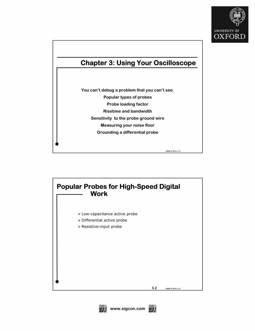
Rise Time of Measured Pulse Depends on Both Probe and Scope Bandwidths
Response of scope and probe to ideal input
Actual risetimeof input signal asloaded by probe
(10-90%)
Probe
Composite responsedisplayed on scope
(10-90%)
Vertical Amplifier
TINPUT TPROBE TINPUT2 + TPROBE
2 + TSCOPE2TSCOPE
TPROBE 0.338/(Probe 3-dB bandwidth)
TSCOPE 0.338/(Scope 3-dB bandwidth)
NOTES:
3.12 HSDD © 2012 v.15
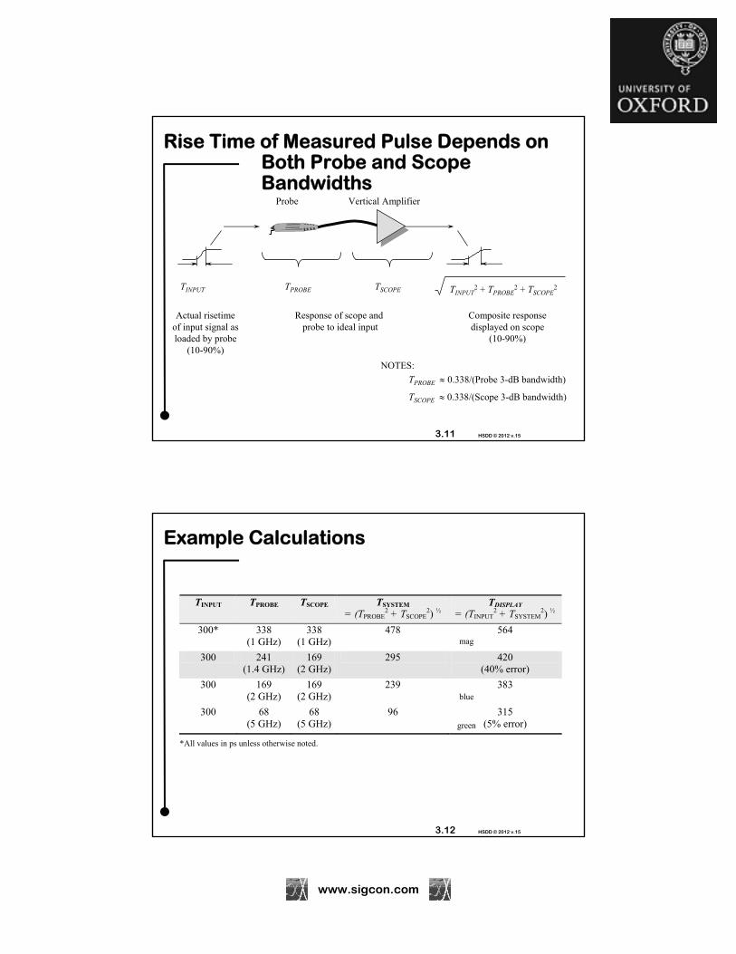
Example Calculations
TINPUT TPROBE TSCOPE TSYSTEM = (TPROBE
2 + TSCOPE2) ½
TDISPLAY
= (TINPUT2 + TSYSTEM
2) ½
300* 338 (1 GHz)
338 (1 GHz)
478
564
300 241 (1.4 GHz)
169 (2 GHz)
295 420 (40% error)
300 169 (2 GHz)
169 (2 GHz)
239 383
300 68 (5 GHz)
68 (5 GHz)
96 315 (5% error)
mag
green
blue
*All values in ps unless otherwise noted.
www.sigcon.com
3.13 HSDD © 2012 v.15
Points to Remember
When figuring a composite rise time, the squares of 10-90% rise time add
A 5-GHz scope with a 5-GHz probe makes a 3.5-GHz instrument
3.14 HSDD © 2012 v.15
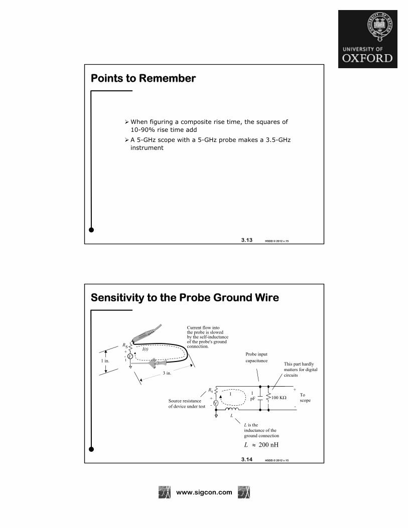
Sensitivity to the Probe Ground Wire
Current flow intothe probe is slowedby the self-inductance of the probe's ground connection.
1 in.
+- V
SRI(t)
L 200 nH
Source resistanceof device under test
L is theinductance of the ground connection
Probe input
capacitance
Toscope
RS
L
+
--
+V
100 KI 1
pF
This part hardlymatters for digital circuits3 in.

www.sigcon.com
3.15 HSDD © 2012 v.15
Ways to ReduceGround Loop Inductance
3 inch ground wire 100-200 nH
3 inch 18 AWG (much fatter wire) 85-170 nH
Short ground attachment 10-20 nH
Knife blade ground 10-20 nH
(Not worth the trouble)
Big, fat knife blade shorts probe ground to pc ground
(big difference)
Short ground attachment pins havefairly low inductance
Tip
Ground Tip
Ground
3.16 HSDD © 2012 v.15
Do These Methods Work?
FET active probe; 1.7 pF; rated 1 GHz; source = 4.7 ohms.
4.7 Ohm Source
1 Volt
1 nS/div
With plastic probe clipand 3" ground wire
Using bare probe tipand 3" ground wire
Using bare probe tipwith probe collar directlygrounded to circuit boardby X-acto knife method
Ground wire
Ground wire
X-acto knife ground
FRES = 1
2 LC

www.sigcon.com
3.17 HSDD © 2012 v.15
Points to Remember
A 1-pF probe looks like 300 ohms to a 1-ns rising edge
A three inch ground wire used with a 1-pF probe induces a 350 MHz resonance
The resonance problem shows up the most when probing low impedance sources
Fattening the ground wire hardly helps with ringing
Radically shortening the ground loop radically improves the ringing response
3.18 HSDD © 2012 v.15
Extra for Experts
Checking for magnetic interference
Checking for ground-current noise
Differential probing
Probing without ground

www.sigcon.com
3.19 HSDD © 2012 v.15
Spurious Magnetic Interference
Ground wire loops pick up noise.
Noise coupled through the probe ground loop is indistinguishable from noise present at the signal node under test.
This additive noise, if synchronous with the signal under test, is difficult to separate from other real features of the signal.
3.20 HSDD © 2012 v.15
How to Tell When Magnetic Pickup Is Going to Be a Problem
Ground the probe to its own tip.
Use the self-grounded probe to look for magnetic fields near printed circuit board.
Don't touch digital logic ground.
Whatever you see willappear superimposed onevery signal you observe.
Using a short ground attachment helpsenormously.
Magneticfield detector

www.sigcon.com
3.21 HSDD © 2012 v.15
Detecting Circulating Ground Currents
Ground the probe to its own tip.
Touch tip and ground together to digital logic ground.
You should see nothing.
If the pcb digital ground and scope ground differ, then current will flow through the probe ground wire, and from there through the probe shield to the scope, generating noise as it goes along.
This ground-current noise appears superimposed on everything you observe.
Using a short ground attachment helps enormously.
Ground-currentdetector
3.22 HSDD © 2012 v.15
Differential Probing
The differential probe doesn’t need a ground wire
Connect the scope to the digital logic ground through other means.
Place both (+) and (-) probes on ground to test for magnetic and ground-current noise.
Place both (+) and (-) probes on a common signal to test for balance.
Signal +
Signal -
PCB Digital Ground

www.sigcon.com
3.23 HSDD © 2012 v.15
Probe Network
For accuracy, the probe impedance should greatly exceed the source and grounding impedances.
3.24 HSDD © 2012 v.15
Broken Ground Makes Measurements Unreliable

www.sigcon.com
3.25 HSDD © 2012 v.15
Points to Remember
Make a magnetic field detector to test for noise induced by mutual inductive coupling.
Touch both probe and ground to digital logic ground to test for noise pickup due to ground currents
Differential probes are not directly grounded to digital logic ground.
Single-ended probes should be grounded at the source.

!!!"#$%&'("&')

www.sigcon.com
HSDD © 2012 v.15
Chapter 4: Transmission Lines
Transmission line impedance and delay
Examples of un-terminated line performance
4.2 HSDD © 2012 v.15
Cross Sections of Popular Transmission Line Geometries
Coaxial cable
Twisted pair
Inner conductor
Jacket (dielectric)
First conductor
Jacket (dielectric)
Second conductor
Inner dielectric
Outer jacket
Outer shield
Stripline
Microstrip
Ground plane
Ground plane
Conductor
Dielectric
Ground plane
Conductor
Dielectric
www.sigcon.com
4.3 HSDD © 2012 v.15
Properties
Transmission lines have many exotic properties, and are the subject of much scientific study.
We will study here only those basic aspects which apply to the practice of distributing high-speed digital signals over copper PCB traces at moderate distances:
Characteristic impedance
Delay
High-Frequency Loss
Crosstalk
4.4 HSDD © 2012 v.15
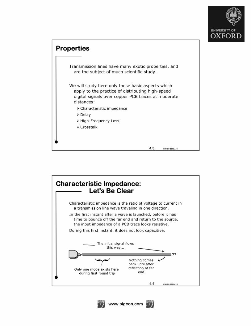
Characteristic Impedance:Let's Be Clear
Characteristic impedance is the ratio of voltage to current in a transmission line wave traveling in one direction.
In the first instant after a wave is launched, before it has time to bounce off the far end and return to the source, the input impedance of a PCB trace looks resistive.
During this first instant, it does not look capacitive.
??Nothing comes back until after reflection at far
endOnly one mode exists here
during first round trip
The initial signal flows this way...

www.sigcon.com
4.5 HSDD © 2012 v.15
Time, ns0 1 2 3 4 5 6 7 8 9 10
-101234
Initial step response at input is flat
Received signal
y(t)
Z0 + RS
x(t) Z0y(t) =
Characteristic Impedance:Response to Step Input
Transmissionline
Capacitiveload = 40pF
+–
RSZ0
–+
RS
y(t)x(t)
z(t)x(t)
Time, ns0 1 2 3 4 5 6 7 8 9 10
-101234
z(t) starts low, then rises to full drive level
Further out in time strange things happen depending on the load...
25= 50
25
4.6 HSDD © 2012 v.15
Ice-Cube Tray Analogy
...Works like an ice-cube tray
The L-C ladder model...

www.sigcon.com
4.7 HSDD © 2012 v.15
Equivalence of Z0 and RTERM
Initial edgezooms by
Nothing reflects from this
arbitrary position
Nothing reflects from this
perfect termination
The driver perceives these circuits as
equivalent.Initial edge
Infinite
4.8 HSDD © 2012 v.15
Approximate Geometries For 50-Ω and 70-Ω Lines
All substratesFR-4; r = 4.5
Microstrip, 70
Stripline, 70
H4
H
2H
Exact Z0 depends on trace thickness and edge finish
H
H
Stripline, 50
1.5
Microstrip, 50
2H
H
2H

www.sigcon.com
4.9 HSDD © 2012 v.15
Relations Between Impedance and Delay
Calculations involving L, C, and tD can be accomplished using per-inch units, or whole-line units.
L = 10 nH/inchC = 2 pF/inch
Z0 = 70tD = 140 ps/inch
H/W = 1:1FR-4 outer layer
+–
+–
0
D
LZ
C
t LC
D 0
D
0
L t Z
tC
Z
L
C
4.10 HSDD © 2012 v.15
Points to Remember
In the first instant after a wave is launched, before it has time to bounce off the far end and return to the source, the input impedance of a PCB trace looks resistive.
PCB trace impedance depends on the ratio of trace width to trace height

www.sigcon.com
4.11 HSDD © 2012 v.15
Effects of Source and Load Impedance
Any combination of source and load impedances connected to a real transmission line will degrade its performance.
The degradation may be slight or it may be devastating.
A good tool for understanding how the source and load interact with a transmission line is the time-space diagram.
4.12 HSDD © 2012 v.15
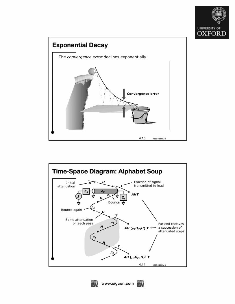
Exponential Decay
Any process, repeatedly attenuated, declines exponentially.
www.sigcon.com
4.13 HSDD © 2012 v.15
Exponential Decay
The convergence error declines exponentially.
Convergence error
4.14 HSDD © 2012 v.15
Bounce
T
T
Bounce again
Fraction of signaltransmitted to load
Same attenuation on each pass
HT
A
AHT2H
1
H
H
H
1
2
2
AH (2H1H) T
AH (2H1H)2 T
Far end receives a succession of attenuated steps
Initial attenuation
Time-Space Diagram: Alphabet Soup
Z0ZS
ZL

www.sigcon.com
4.15 HSDD © 2012 v.15
Step 1
Step 2
Step 3
Evolution of Transmission Line Response
Z0ZS
ZL
T
T
HT
A
2H
1
H
H
H
1
2
2
Time
Time
Volts
Space
4.16 HSDD © 2012 v.15
A Ringing Waveform Decays Exponentially
Decay envelope = kn
Round-trip delay
Final value
k
k2
k3
k4
k5
Any damped process converges given enough time.
Convergenceerror

www.sigcon.com
4.17 HSDD © 2012 v.15
Mathematical Convergence Relation
(12H2) Exponential convergence factor (roundtrip)
N Number of round-trips
E Permitted fractional settling error
Ways to improve performance
Reduce 1 (source termination)
Reduce 2 (end termination)
Increase N (short-line method)
Decrease H (increase line attenuation)
(12H2)N < E
k
4.18 HSDD © 2012 v.15
The Reflection Function,
1/100 1/10 1 10 100-1
-0.5
0
0.5
1
Normalized termination coefficient ZL/Z0
Reflection coefficient
Reflections never exceed the size of the incoming signal: | | < 1
23
1/21/3
(1+) A matching ratio of 110% yields a reflection of 5%.
Even a horrible matching ratio, like 3:1, still produces a reflection of only 50%.
0.330.50
-0.33-0.50
/2

www.sigcon.com
4.19 HSDD © 2012 v.15
Reflection Chart
A 10% termination mismatch causes a 5% reflection
A mismatch of 3:1 absorbs half the incoming signal (-6 dB)
Coefficient T often exceeds unity
Z0
T(w)
ZL(w)
Unit step inputZL
Z0
ZL - Z0
ZL + Z0
T = 1 +
0 -1 0
1/3 -1/2 1/2
1/2 -1/3 2/3
0.90 -0.05 0.95
1.00 - 1.00
1.10 +0.05 1.05
2 +1/3 4/3
3 +1/2 3/2
+1 2
=
4.20 HSDD © 2012 v.15
Example: Un-Terminated Line Performance
Source impedance too low
(RS < Z0)
Source impedance too high
(RS > Z0)

www.sigcon.com
4.21 HSDD © 2012 v.15
Low Source Impedance
Reflection at far end is positive (2 = +1)
Reflection at source end is negative (1 = -1/2 )
Signal alternates polarity each round trip
RS = 17
50
A = 3/40.750
HT = 2
1.50 First incident wave
Roundtrip time = 2tD
Open circuit at end
H
1 = -1/2
-0.375
-0.75+1
-0.375-1/2
+0.187
Total result for perfect step input
Third
Second
2 = +1H 0.750
4.22 HSDD © 2012 v.15
Step Response of Unterminated Line With Low Source Impedance
Reflection at far end is positive, at source end is negative
Signal alternates polarity each round trip
One round-trip delay
Final value 1.00
Initial stepis too big
Exponential decay envelope
2 Z0
RS + Z0
RS = 17
www.sigcon.com
4.23 HSDD © 2012 v.15
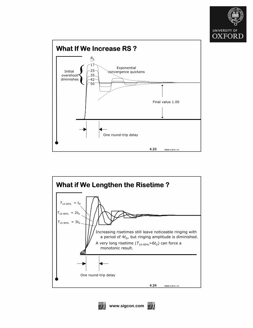
What If We Increase RS ?
One round-trip delay
RS
Final value 1.00
Initial overshootdiminishes
50423525
17Exponential
convergence quickens
4.24 HSDD © 2012 v.15
What if We Lengthen the Risetime ?
Increasing risetimes still leave noticeable ringing with a period of 4tD, but ringing amplitude is diminished.
A very long risetime (T10-90%>6tD) can force a monotonic result.
One round-trip delay
T10-90% = tD
T10-90% = 2tD
T10-90% = 3tD

www.sigcon.com
4.25 HSDD © 2012 v.15
High Source Impedance
Reflection at far end is positive (2 = +1)
Reflection at source end is positive (1 = +1/2)
Signal accumulates with same polarity each round trip
Open circuit at end
1 = +1/2
H0.125
First incident wave
Roundtrip time = 2tD
Second
Third
Total result for perfect step input
50
RS = 150
HT = 2
A = 1/40.250
0.500
2 = +1H
0.250
4.26 HSDD © 2012 v.15
Step Response of Un-terminated Line With High Source Impedance
Reflection at both ends is positive
Signal accumulates monotonically
One round-tripdelay
Final value 1.00
Initial stepis too small
2 Z0
RS + Z0
Monotonic exponentialbuild-up
Reminds me of a stegosaurus
Copy right 1996 Joe Tucciarone & Jeff Poling
RS = 150

www.sigcon.com
4.27 HSDD © 2012 v.15
Try Reducing RS
One round-trip delay
Final value 1.00
Convergence time improves assource impedance is reduced.
150
100
705850
RS
Z0 = 50 remains fixed as wetry different value of source impedance.
Start
4.28 HSDD © 2012 v.15
Try Raising Z0
One round-trip delay
Final value 1.00
Convergence time improves whenyou fix the ratio RS/Z0
50
75
107130150
Z0
This time, RS = 150 remains fixed while we vary the line impedance.
Start
All that matters is this ratio: RS/Z0

www.sigcon.com
4.29 HSDD © 2012 v.15
What if We Lengthen Risetime ?
One round-trip delay
Final value 1.00Resembles R-Crelaxation withT0-63%=RC
This is the source of the myth thatthe input to a transmission line looks
like a capacitive load
T10-90% = tD
T10-90% = 2tD
T10-90% = 3tD
Steps easily mush together
4.30 HSDD © 2012 v.15
Points to Remember
Source impedance too low: Ringing
(RS < Z0)
Initial step too big (overshoot)
Source impedance too high: Stegosaurus
(RS > Z0)
Initial step too small (doesn’t meet VOH)
End chapter 4.

www.sigcon.com
4.31 HSDD © 2012 v.15
Capacitive Loading
Extra for Experts
4.32 HSDD © 2012 v.15
Remember This Circuit?
T10-90% = 1 ns
1-in. trace10Load
= 6 in.Z0 = 65 ohmdelay = 1/6 ns
Remember this?
Load (optional)
L"π" model
½C ½C
It acts like this:
10 10 nH
1 pF 1 pF10 pF
T10-90% = 1 ns
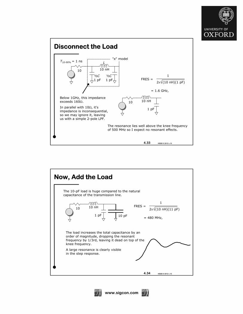
www.sigcon.com
4.33 HSDD © 2012 v.15
Disconnect the Load
L"π" model
½C ½C
10 10 nH
1 pF 1 pF
Below 1GHz, this impedance exceeds 160.
In parallel with 10, it's impedance is inconsequential, so we may ignore it, leaving us with a simple 2-pole LPF.
10 10 nH
1 pF
T10-90% = 1 ns
FRES =2 (10 nH)(1 pF)
1
= 1.6 GHz,
The resonance lies well above the knee frequency of 500 MHz so I expect no resonant effects.
4.34 HSDD © 2012 v.15
Now, Add the Load
10 10 nH
1 pF
FRES =2 (10 nH)(11 pF)
1
= 480 MHz,
The load increases the total capacitance by an order of magnitude, dropping the resonant frequency by 1/3rd, leaving it dead on top of the knee frequency.
A large resonance is clearly visiblein the step response.
10 pF
The 10-pF load is huge compared to the natural capacitance of the transmission line.

!!!"#$%&'("&')

www.sigcon.com
HSDD © 2012 v.15
Chapter 5: Solid Plane Layers
Intuition about crosstalk and return current
Ground plane slots
Guard traces
Split power planes
Ground isolation regions
5.2 HSDD © 2012 v.15
Early Computers Had No Solid Planes

www.sigcon.com
5.3 HSDD © 2012 v.15
Microstrip Response to Changing Magnetic Field
5.4 HSDD © 2012 v.15
Microstrip Crosstalk
These lines of flux create crosstalk.
www.sigcon.com
5.5 HSDD © 2012 v.15
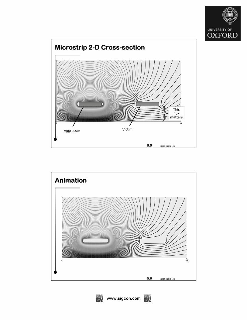
Microstrip 2-D Cross-section
Aggressor Victim
This flux
matters
5.6 HSDD © 2012 v.15
Animation

www.sigcon.com
5.7 HSDD © 2012 v.15
251 mV for T10-90% < 2(trace delay)
26 mV/inch at T10-90% = 1 ns
148 mV for T10-90% < 2(trace delay)
19 mV/inch at T10-90% = 1 ns
NEXT
FEXT
Board #1 Board #2
Do Not Give Your PCB Vendor Full Control Over H and W
These boards have the same trace impedance, but…
Crosstalk varies strongly with H, so
Board #2 has substantially more NEXT than board #1
W=.005H=.005
W=.007
H=.007
D=.015 D=.015
Same finishedthickness Same W/H
Same Z0
VCC = 3.3V
5.8 HSDD © 2012 v.15
How Much Can You Take?
VCC MIN
VOH
VIH
0V
VOL
VIL
VCC
DriverPackagedreceiver
Die thresholds(JEDEC 3.3V CMOS)
PowerSystem
Board-level ringing, crosstalk, ground shifts and other noise
Crosstalk (ground bounce) within package
Driver R[OUT]
–10%
6%8%
=200 mV

www.sigcon.com
5.9 HSDD © 2012 v.15
Points to Remember
A solid plane is a very good defense against crosstalk.
The closer you place your traces to the plane, the less crosstalk you will suffer.
5.10 HSDD © 2012 v.15
Where Simulation Fails Us
Signal integrity simulators do well predicting crosstalk ASSUMING
Solid reference plane layers under every trace
Perfect layer transitions
No cuts, separations or slots in the reference planes

www.sigcon.com
5.11 HSDD © 2012 v.15
The Path of Return Signal Current
High-speed current follows the path of least inductance
At low speeds, currentfollows the path of least resistance
At high speeds, return currentstays tightly bunched undersignal trace
5.12 HSDD © 2012 v.15
The High-Speed Path Can Look Pretty Strange
Signal current
Return current
Return currentcirculates all the way around the loop—it does not cut the corner.
VTT

www.sigcon.com
5.13 HSDD © 2012 v.15
Distribution of High-Frequency Current Underneath a Signal Trace
Cross-sectional viewof microstrip
Dhorizontaldistance
H
W
Reference plane
H1 +
1
D 2Trace
Stray current density in the tails varies in rough proportion to:
Magnetic fields fromstray current causecrosstalk
5.14 HSDD © 2012 v.15
What about Capacitance?
When low-impedance traces come out of the board on package pins, connectors, or other exposed wiring, inductive crosstalk dominates.
Between two long, parallel traces within a homogeneous dielectric, inductive and capacitive remain in balance.
Fortunately, in this situation capacitive crosstalk follows the same 1/D2 law as inductive crosstalk.
Therefore, all we really have think about, for crosstalk between low-impedance circuits, is inductive crosstalk.

www.sigcon.com
5.15 HSDD © 2012 v.15
Crosstalk Versus Trace Separation Experiment
50 Ω 50 Ω
50 Ω
Aggressor
Victim
Pulse generator D is variable
D = trace-to-trace horizontal centerline pitch, inchesH = centerline height of traces above ground (0.016”)overlap region = 330 ps in length (2”)
Solid ground plane
37 MHz clock 3V p-p
T10-90% = 2.5 ns
5.16 HSDD © 2012 v.15
Crosstalk Over a Solid Ground Plane
0 10 20 30 40 50–0.4
–0.3
–0.2
–0.1
0
0.1
0.2
0.3
0.4
Time, ns
Volts
D/H = 2D/H = 4
D/H = 8
Tektronix 7000 series
Crosstalk falls off as 1/D2
Aggressor signal: 3v p-p

www.sigcon.com
5.17 HSDD © 2012 v.15
Crosstalk Over a Solid Ground Plane
Ratio (D/H) of trace pitch to trace height
Crosstalk picked up in 330 ps
overlap region(mV)
1 10 1000.1
1
10
100
1/D2
Stripline Crosstalk Study
H2
H1
The effective height:
H =1
+H1
1
H2
1

www.sigcon.com
Stripline Crosstalk Versus Separation
NOTE: H is the "effective height"
5.20 HSDD © 2012 v.15
Crosstalk Versus Trace Separation
Microstrip Stray current density falls off with 1/D2 as we move
away from the signal conductor
Stray current causes crosstalk
Therefore, crosstalk falls off with 1/D2 as we separate two traces
Separating traces over a solid ground plane is the most effective way to combat crosstalk
StriplineCrosstalk falls off even more rapidly with distance
www.sigcon.com
5.21 HSDD © 2012 v.15
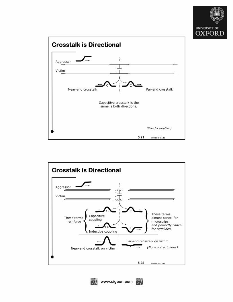
C
Aggressor
Victim
Crosstalk is Directional
Near-end crosstalk Far-end crosstalkC
(None for striplines)
Capacitive crosstalk is the same is both directions.
5.22 HSDD © 2012 v.15
Capacitive coupling
Inductive coupling
+L
Crosstalk is Directional
Near-end crosstalk on victim
Far-end crosstalk on victim
These terms reinforce
These terms almost cancel for microstrips,and perfectly cancel for striplines.
+ –
–L
(None for striplines)
C
Aggressor
Victim
C

www.sigcon.com
5.23 HSDD © 2012 v.15
Points to Remember
Both signal and return currents are equally capable of generating crosstalk.
If you provide a solid reference plane your return current will use it, staying generally underneath the signal trace.
Crosstalk is VERY sensitive to the spacing and height of your traces.
Get a crosstalk simulation tool.
5.24 HSDD © 2012 v.15
Ground Plane Slots
Ground slots happen most often about 3:00 am, when someone runs out of room on the regular routing layers.
They cut a long narrow slot in the solid plane layer and place the trace in the slot.
Slots destroy the effectiveness of your solid plane layer.
www.sigcon.com
5.25 HSDD © 2012 v.15
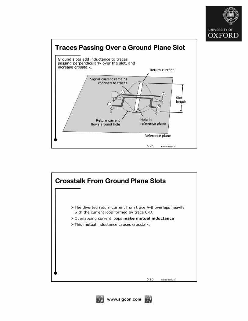
Traces Passing Over a Ground Plane Slot
Ground slots add inductance to traces passing perpendicularly over the slot, and increase crosstalk.
C
A
D
B
Signal current remains confined to traces
Return current flows around hole
Hole in reference plane
Reference plane
Slot length
Return current
5.26 HSDD © 2012 v.15
Crosstalk From Ground Plane Slots
The diverted return current from trace A-B overlaps heavily with the current loop formed by trace C-D.
Overlapping current loops make mutual inductance
This mutual inductance causes crosstalk.

www.sigcon.com
5.27 HSDD © 2012 v.15
Connector Layout Slots
Ground slots also happen on dense back planes which pass through fields of connector pins.
Always make sure the ground clear-outs around each pin have ground continuity between all pins.
Clear-out holesfor connectorpins are too big;ground is not continuous throughthe pin field
Return signalcurrent mustflow aroundthe pin field
Return signalcurrent flowsstraight throughthe pin field
Groundplane
Clear-out holesfor connectorpins are OK
5.28 HSDD © 2012 v.15
Crosstalk Versus Trace Separation: Over a Ground Plane Slot
50 Ω 50 Ω
50 Ω
Aggressor
Victim
Pulse generatorD is variable
D = trace-to-trace pitch (centerline-to-centerline), inchesH = height of traces above ground (0.016”)overlap region = 330 ps in length
Two solid ground planes;either one or both may have a slot
Planes are stitchedtogether all around edges
37 MHz clock 3V p-p
T10-90% = 2.5 ns
www.sigcon.com
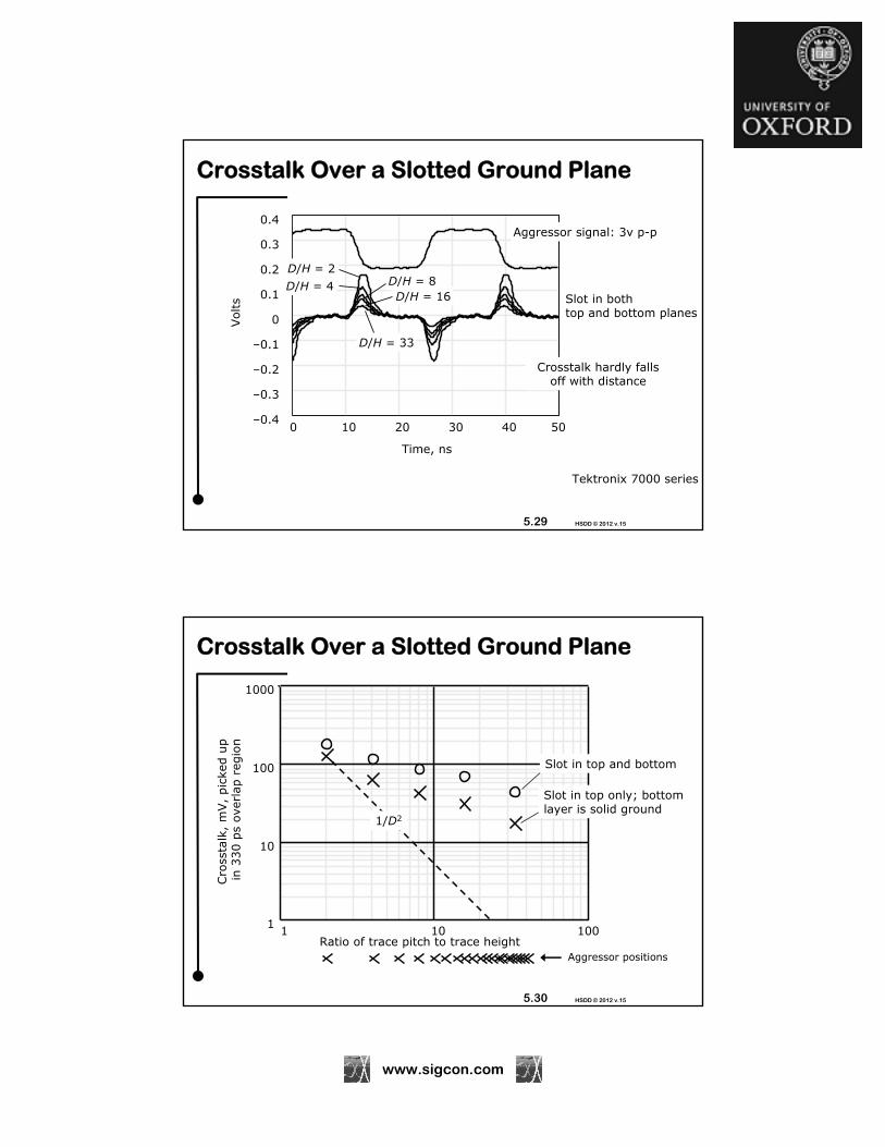
5.29 HSDD © 2012 v.15
Crosstalk Over a Slotted Ground Plane
0 10 20 30 40 50–0.4
–0.3
–0.2
–0.1
0
0.1
0.2
0.3
0.4
Time, ns
Volts
Aggressor signal: 3v p-p
D/H = 2
D/H = 4 D/H = 8D/H = 16
D/H = 33
Crosstalk hardly falls off with distance
Slot in bothtop and bottom planes
Tektronix 7000 series
5.30 HSDD © 2012 v.15
Crosstalk Over a Slotted Ground Plane
1 10 1001
10
100
1000
Ratio of trace pitch to trace height
Cro
ssta
lk,
mV,
pic
ked u
pin
330 p
s ove
rlap
reg
ion
Slot in top only; bottomlayer is solid ground
Slot in top and bottom
Aggressor positions
1/D2
www.sigcon.com
5.31 HSDD © 2012 v.15
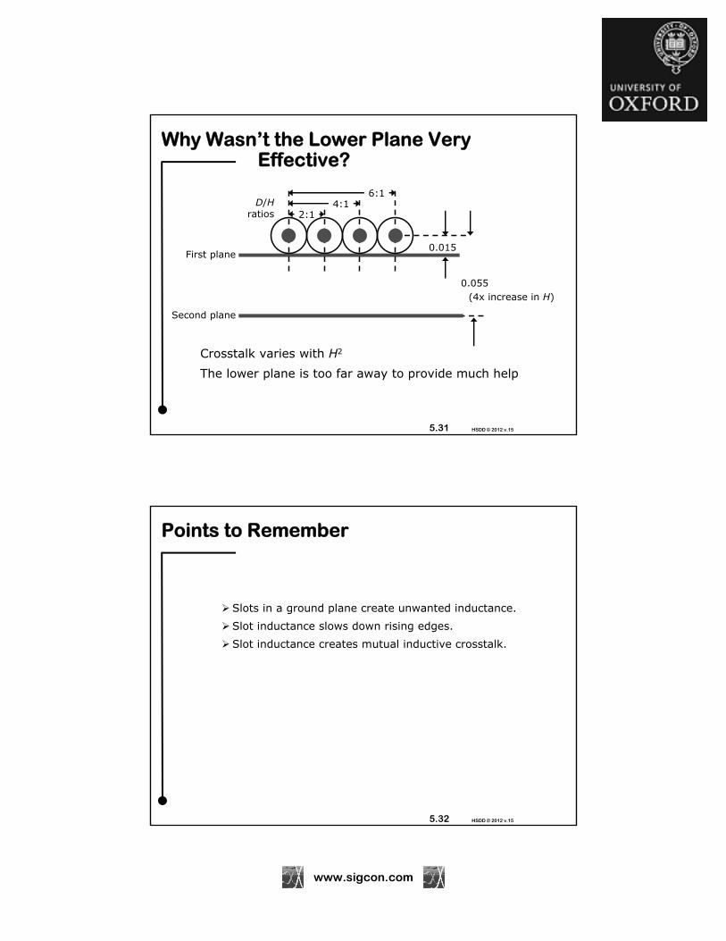
Why Wasn’t the Lower Plane Very Effective?
Crosstalk varies with H2
The lower plane is too far away to provide much help
D/Hratios 2:1
4:16:1
0.015
0.055(4x increase in H)
First plane
Second plane
5.32 HSDD © 2012 v.15
Points to Remember
Slots in a ground plane create unwanted inductance.
Slot inductance slows down rising edges.
Slot inductance creates mutual inductive crosstalk.
www.sigcon.com
5.33 HSDD © 2012 v.15
These techniques save layers, but…
Not for high-speed digital design.
Ye Olde Non-Continuous Grounde Plaenes (1980)
Still used in low-speed and analog products
Power and ground fingers
Cross-hatched ground grid
We will use these old examples to build your general knowledge of crosstalk.
5.34 HSDD © 2012 v.15
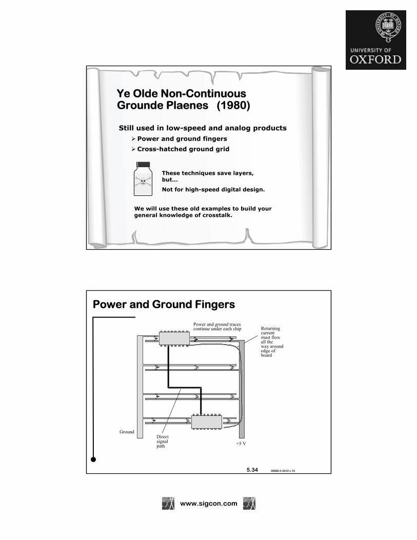
Power and Ground Fingers
Returningcurrentmust flowall theway around edge ofboard
Power and ground tracescontinue under each chip
GroundDirectsignalpath +5 V

www.sigcon.com
5.35 HSDD © 2012 v.15
+5 VGround Top layer
Backlayer
Trace
length
Y
Returningcurrent mustfollow powerand groundwires, stayingclose tooutgoing signalpath
Cross-hatchedspacing isthe same inboth directions
Tracewidth is
X
Directsignalpath
W
These horizontal members
underneath the verticaltraces
are continuous, passing
Cross-Hatched Ground Grid
5.36 HSDD © 2012 v.15
+5 VGround Top layer
Backlayer
New return path
Directsignalpath
These horizontal members
underneath the verticaltraces
are continuous, passing
Guard Trace Helps a Two-Layer Board

www.sigcon.com
5.37 HSDD © 2012 v.15
Ordinary Microstrip Crosstalk
5.38 HSDD © 2012 v.15
Make Room for the Guard Trace
0 dB
Gained a factor of
four!
www.sigcon.com
5.39 HSDD © 2012 v.15
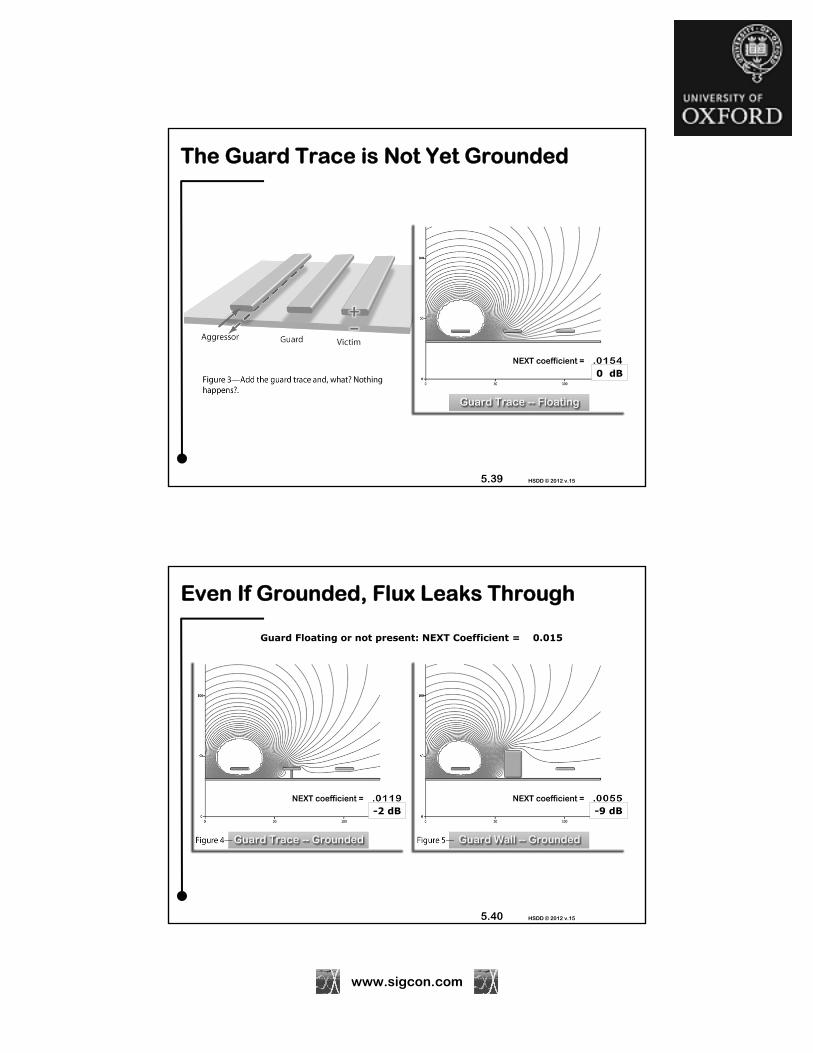
The Guard Trace is Not Yet Grounded
0 dB
5.40 HSDD © 2012 v.15
Even If Grounded, Flux Leaks Through
Guard Floating or not present: NEXT Coefficient = 0.015
-2 dB -9 dB

www.sigcon.com
5.41 HSDD © 2012 v.15
Guards Appear More Effective at Ridiculous Heights
+9 dB+16 dB
5.42 HSDD © 2012 v.15
Points to Remember
Crosstalk arises whenever the signal path separates from its return path.
If you already have solid planes in your board, do not mess around with guard traces—just use rules of spacing to control crosstalk.

www.sigcon.com
5.43 HSDD © 2012 v.15
Crossing a Split Power Plane Boundary
PCB cross section
Returning current can’t get across the slot;
GND
+3.3V+2.5V
5.44 HSDD © 2012 v.15
Crossing a Split Power Plane Boundary
Returning current diverts through bypass capacitors.
GND
+3.3V+2.5V
www.sigcon.com
5.45 HSDD © 2012 v.15
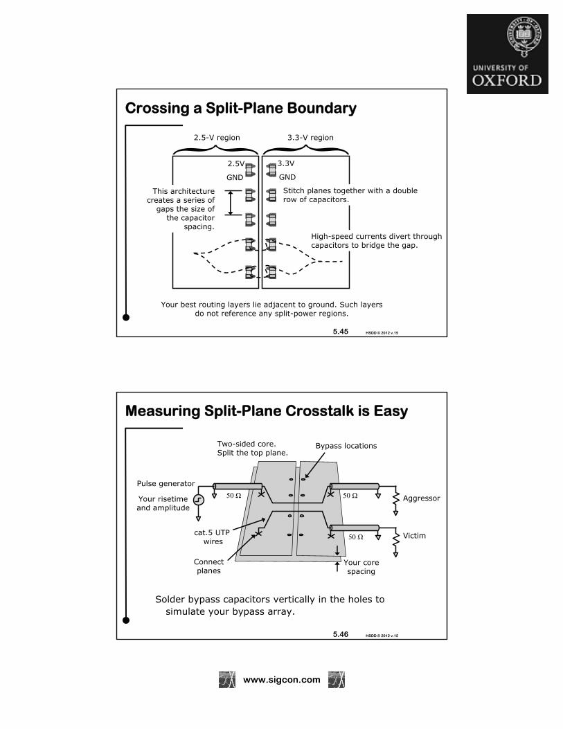
Crossing a Split-Plane Boundary
2.5-V region 3.3-V region
3.3V2.5V
GND GND
High-speed currents divert through capacitors to bridge the gap.
Stitch planes together with a double row of capacitors.
Your best routing layers lie adjacent to ground. Such layers do not reference any split-power regions.
This architecture creates a series of
gaps the size of the capacitor
spacing.
5.46 HSDD © 2012 v.15
Measuring Split-Plane Crosstalk is Easy
Solder bypass capacitors vertically in the holes to simulate your bypass array.
Aggressor
Victim
Pulse generator
Two-sided core.Split the top plane.
Your risetimeand amplitude
50 Ω
50 Ω
50 Ω
cat.5 UTP wires
Bypass locations
Connect planes
Your core spacing

www.sigcon.com
5.47 HSDD © 2012 v.15
Implications for Signal Routing With300 ps Edges And Faster
Return current cannot simply jump between widely separated planes.
5.48 HSDD © 2012 v.15
Implications for Signal Routing With300 ps Edges And Faster
Bypass capacitors convey returning signals currents between planes wherever the signal path penetrates the layer stack.
www.sigcon.com
5.49 HSDD © 2012 v.15
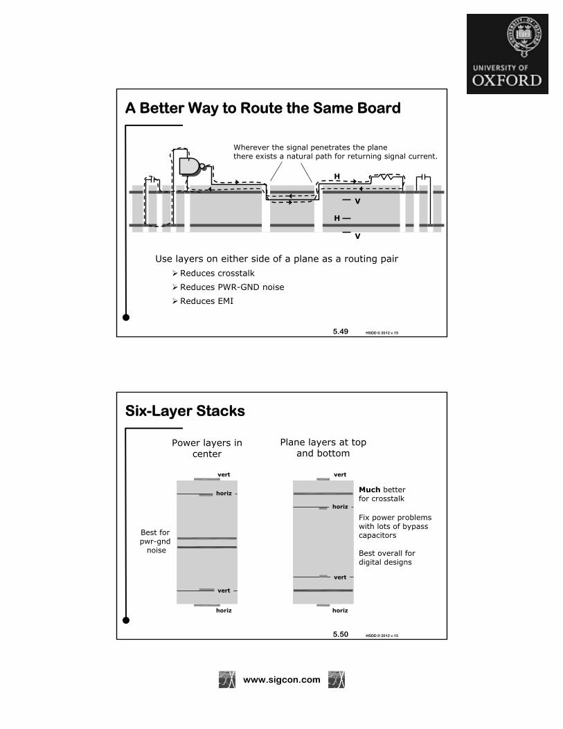
A Better Way to Route the Same Board
Use layers on either side of a plane as a routing pair
Reduces crosstalk
Reduces PWR-GND noise
Reduces EMI
Wherever the signal penetrates the planethere exists a natural path for returning signal current.
H
V
H
V
5.50 HSDD © 2012 v.15
Six-Layer Stacks
horiz
horiz
vert
vert
Plane layers at top and bottom
Power layers in center
horiz
horiz
vert
vert
Best for pwr-gnd
noise
Much better for crosstalk
Fix power problems with lots of bypass capacitors
Best overall for digital designs

www.sigcon.com
5.51 HSDD © 2012 v.15
NASA* Layer Stack
*Only NASA can afford this...
Ground planes sandwich the power layer
0.063-in. totalthickness
0.005
0.005
0.005
0.005
0.005
0.005
0.005
Layer 9: 0.005-in. width, 0.015-in pitch,50 Ω (offset stripline)
Layer 10: 0.005-in. width, 0.015-in. pitch,50 Ω (offset stripline)
Layer 14: 0.008-in. width, 0.015-in. pitch,50 Ω (microstrip)
Layer 1: 0.010-in. width, 0.015-in. pitch,50 Ω (microstrip)
Layer 5: 0.005-in. width, 0.015-in. pitch,50 Ω (offset stripline)
Layer 2: ground plane
Layer 6: 0.005-in. width, 0.015-in. pitch,50 Ω (offset stripline)core
core
core
0.005
0.005
core
0.002
0.002
0.005
0.002
Layer 3: power planeLayer 4: ground plane
Layer 7: funky power planeLayer 8: ground plane
Layer 11: ground planeLayer 12: power planeLayer 13: ground plane
horiz
vert
horiz
vert
horiz
vert
core
core
5.52 HSDD © 2012 v.15
Good High-Speed Practices for Big, Fat Boards

www.sigcon.com
5.53 HSDD © 2012 v.15
When to Segment the VCC Plane
IC's with the same logic levels, and the same sensitivity to noise, tie together to a common set of Vcc/Gnd planes.
Use separate regions for:
IC's with different power voltages
PLL's or clock generators with special sensitivity to power supply noise
I/O chips that must not have noise on their power terminals
5.54 HSDD © 2012 v.15
Place Your Special Power Region in a Corner of the PCB
Make slot 20H wide
Special power region
Regular VCC
Ground
Inductor or VRM feeds special region
Capacitors control noise only with respect to local ground.

www.sigcon.com
5.55 HSDD © 2012 v.15
Extra For Experts
Crosstalk NEXT and FEXT examples
5.56 HSDD © 2012 v.15
NEXT and FEXT Can Be Separately Measured
Aggressor
VictimNEXT(t) FEXT(t)
tD
NEXT is a positive pulse with a duration of (2tD + T10-90%).
FEXT for microstrips is a negative pulse with a duration of T10-90%.
FEXT for striplines is zero.

www.sigcon.com
5.57 HSDD © 2012 v.15
Stretching the Trace Length
100
mV
/div
1 nsec/div
FR-4 substrateZ0=64 ohms3.3-CMOST10-90% = 1 nsD/H = 15/7 = 2.14 Area(FEXT)/Area(NEXT) = 0.31
D=15
W=7H=7
Aggr. Victim
NEXT
FEXT
Crosstalk for parallel runs of1/2, 1, 2, 4, 8 and 16 inches
265 mV
HyperLynx LineSim
NEXT duration grows linearly with trace lengthFEXT amplitude grows linearly with trace length
5.58 HSDD © 2012 v.15
Moving Closer to the Reference Plane
100
mV
/div
1 nsec/div
NEXT
FEXT
Crosstalk for parallel runs of1/2, 1, 2, 4, 8 and 16 inchesD=15
W=5H=5
Aggr. Victim
FR-4 substrateZ0=64 ohms3.3-CMOST10-90% = 1 nsD/H = 15/5 = 3.00 Area(FEXT)/Area(NEXT) = 0.42
155 mV
HyperLynx LineSim
NEXT changes quadratically with HFEXT changes quadratically with H

www.sigcon.com
5.59 HSDD © 2012 v.15
Separating the Traces
100
mV
/div
1 nsec/div
NEXT
FEXT
Crosstalk for parallel runs of1/2, 1, 2, 4, 8 and 16 inches
FR-4 substrateZ0=64 ohms3.3-CMOST10-90% = 1 nsD/H = 25/5 = 5.00 Area(FEXT)/Area(NEXT) = 0.58
D=25
W=5H=5
Aggr. Victim
55 mV
NEXT changes quadratically with 1/DFEXT changes quadratically with 1/D
HyperLynx LineSim
5.60 HSDD © 2012 v.15
D=15
W=5H1=9
Aggr. Victim
H2=21
Striplines Have No FEXT
Here we’ve changed to a a 5-mil microstrip with 15-mil pitch. The reference plane heights have been adjusted to create 65-ohm traces.
High frequency losses will be similar to the 5x5 microstrip.
The D/H ratio is similar to the 7x7 D=15 microstrip, so you will get similar amounts of NEXT, but no FEXT.
H(effective) 1/(1/9 + 1/21) = 6.3D/H = 15/6.3 = 2.38
100
mV
/div
1 nsec/div
Crosstalk for parallel runs of1/2, 1, 2, 4, 8 and 16 inches
NEXT
No FEXT
263 mV
HyperLynx LineSim

www.sigcon.com
5.61 HSDD © 2012 v.15
How NEXT Becomes a Far-End Problem
Aggressor
Victim
The aggressive signal creates NEXT that proceeds towards the source.
FEXT(t) + NEXT(t-tD)
tD
The NEXT bounces off the victim driver and finally appears at the far end.
t
The receiver gets a combination of both FEXT and NEXT.
5.62 HSDD © 2012 v.15
It Doesn’t Help to Use Source-Termination
Aggressor
Victim
Along the way back, it creates some NEXT
The aggressive signal goes out
t
Which ends up at the receiver.
And bounces off the endpoint

www.sigcon.com
5.63 HSDD © 2012 v.15
FR-4 substrateZ0=64 ohms3.3-CMOST10-90% = 1 nsD/H = 15/5 = 3.00
FEXT + NEXT at End of Line
NEXT(reflected)
FEXT
Aggregate
100
mV
/div
1 nsec/div
FEXT+NEXT for parallel runs of1/2, 1, 2, 4, 8 and 16 inchesD=15
W=5H=5
Aggr. Victim
Waveforms have been time-aligned for clarityEnd termination is used.
HyperLynx LineSim
5.64 HSDD © 2012 v.15
The Both-Ends Termination Kills NEXT
Aggressor
Victim
Along the way out, it creates some NEXT...
The aggressive signal goes out...
t
...And dies at the endpoint.
...That dies at the source.
NEXT never reaches the receiver.

www.sigcon.com
5.65 HSDD © 2012 v.15
Bonus Question
In a case with weak crosstalk coupling, what happens if the victim is left un-terminated?
5.66 HSDD © 2012 v.15
Factors That Influence Crosstalk
Most powerful factors
Move traces closer to the nearest reference plane (and make them skinnier to keep impedance constant)
Move traces further apart
Reduce amplitude of the aggressor
Special factors applicable onlywhen risetime exceeds roundtrip delay
Reduce length of the parallelism
Slow down the rise/fall time
Systemic factors
Use stripline (kills FEXT)
Use both-ends termination (kills NEXT)

!!!"#$%&'("&')
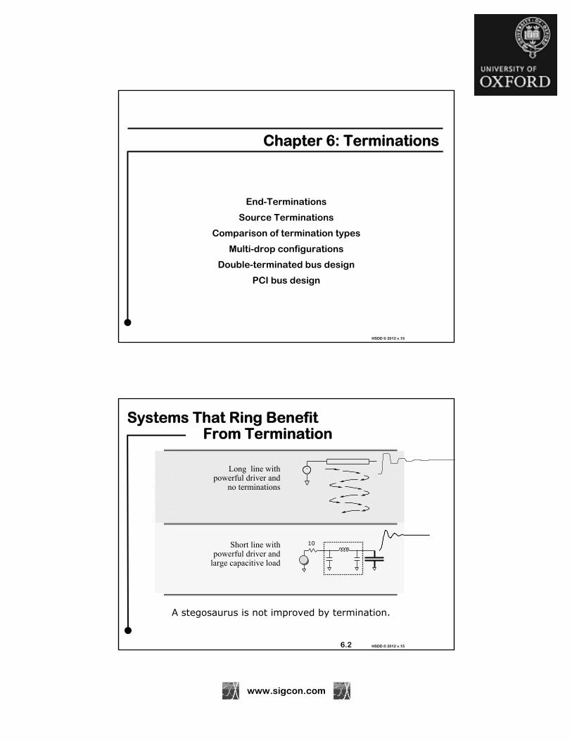
www.sigcon.com
HSDD © 2012 v.15
Chapter 6: Terminations
End-Terminations
Source Terminations
Comparison of termination types
Multi-drop configurations
Double-terminated bus design
PCI bus design
6.2 HSDD © 2012 v.15
Systems That Ring Benefit From Termination
-+Long line with
powerful driver andno terminations
Short line with powerful driver and
large capacitive load
10
A stegosaurus is not improved by termination.

www.sigcon.com
6.3 HSDD © 2012 v.15
Standard Ways to Stop Reflections
End termination
Series termination
Both ends termination
Any of these approaches can prevent problems withlong-line reflections or short-line ringing
Most popular styles for digital logic
6.4 HSDD © 2012 v.15
End Termination
Uses terminating resistor at far end.
Sets far end reflection to zero.
End terminations dissipate a lot of static power.
Z0
Low impedance at source
2 = 0
Practically nothingsurvives the first reflection
RT = Z0
A = 1
T = 1

www.sigcon.com
6.5 HSDD © 2012 v.15
Function of Split Termination
The values R1 and R2 in the split termination set the amount of driver current required in the LO (and HI) states of operation.
Z0
IOL = - (VCC - VOL) / R1 - VOL/R2
R1VOLVOL
R2
VCCI+
I-
LO state
-IOL
6.6 HSDD © 2012 v.15
Design Constraints
Tradeoff HI and LO drive current requirements to match gate capabilities
Constraints:
(R1 R2)/(R1 + R2) = Z0
Don’t exceed IOL max
Don’t exceed IOH max
VCC
Z0
R2
VCC
R1
R1 in parallel with R2should equal Z0 ohms
A two-variable optimization problemwith three constraints (one of which is non-linear).

www.sigcon.com
6.7 HSDD © 2012 v.15
Mental Image of Split Terminator
Think of the split terminator as a single resistor, of value RT=Z0, connected to a battery.
Setting VT higher makes it easier to drive high, but harder to drive low
Setting VT lower makes it easier to drive low, but harder to drive high
Setting VT in the middle makes it equally difficult to drive high or low
RT
VT
Values R1 and R2 in the split terminator determine the battery voltage.
6.8 HSDD © 2012 v.15
Design Process
1. Set resistor value equal to Z0
2. Adjust VT to satisfy IOL max and IOH max
3. Simple equations convert (RT, VT) into split-terminator topology
VCC
GND
R1
R2
…then transform to this...
RT
VT
First design this…

www.sigcon.com
6.9 HSDD © 2012 v.15
Solve for VT and RT
If ZMIN < Z0 , solutions exist for RT = Z0 .
If ZMIN > Z0, solutions exist only for RT ZMIN .
Whatever value you pick for RT, make sure VT falls between the solution constraints [1] and [2].
VT > VOH - IOHRT
VT < VOL - IOLRT
High drive condition
Low drive condition
ZMIN=
Solution constraints for VT (final-value current conditions):
Always check this quantity:
IOH - IOL
VOH - VOL ZMIN is the smallest impedance a gate can safely drive.
[1]
[2]
[3]
Solutions exist only for RT ZMIN
6.10 HSDD © 2012 v.15
Transform Back to Split Topology
VCC
GND
R1 = RT
VCC
VT
R2 = RT
VCC
VCC - VT
RT
VT…do this...
Given VT and RT :

www.sigcon.com
Time
Voltage
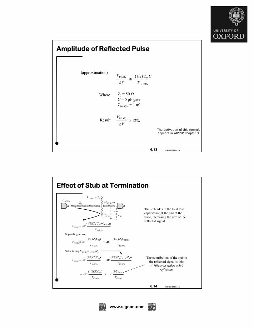
www.sigcon.com
6.13 HSDD © 2012 v.15
Amplitude of Reflected Pulse
(approximation)
Z0 = 50 ΩC = 5 pF gate T10-90% = 1 nS
12%
(1/2) Z0 C
T10-90%
Where
Result
VPEAK
V
VPEAK
VThe derivation of this formulaappears in AHSSP chapter 3.
6.14 HSDD © 2012 v.15
Effect of Stub at Termination
T10-90%Z0
CINCSTUB
VPEAK V(1/2)(Z0(CIN+CSTUB))
T10-90%
RTERM Z0
Substituting CSTUB = tSTUB/Z0,
VPEAK V(1/2)(Z0CIN)
T10-90%
+ V(1/2)(Z0(tSTUB/Z0))
T10-90%
= V(1/2)(Z0CIN)
T10-90%
+ V(1/2)tSTUB
T10-90%
The contribution of the stub to the reflected signal is this:A 10% stub makes a 5%
reflection.
The stub adds to the total load capacitance at the end of the trace, increasing the size of the reflected signal.
tSTUB
VPEAK V(1/2)(Z0CIN)
T10-90%
+ V(1/2)(Z0CSTUB)
T10-90%
Separating terms,

www.sigcon.com
6.15 HSDD © 2012 v.15
Points to Remember
Split terminations trade off I[OH] against I[OL].
The lowest impedance an I/O circuit can drive equals:
Capacitance at the receiver creates unwanted reflections.
OH OLMIN
OH OL
V V
ZI I
6.16 HSDD © 2012 v.15
Series Termination (Source Termination)
Signal is cut in half by source resistor
First edge (half amplitude)
Signal doubles, appearing atnormal size as it bounces off open-circuited endpoint
Reflected signal travels back towards source still at half amplitude
Reflection dies at source resistor; drive current drops to zero
A = 1/2
T = 2
2 = +1
Series terminations dissipate power only on signal transitions
R = Z0
VCC
Z0
Reflected edge
Full height
t v(t)
1 = 0

www.sigcon.com
6.17 HSDD © 2012 v.15
Signal Near Endpoint
Signal is cut in half by source resistor
First edge (half amplitude)
Reflected signal is still half-sized
Reflection dies at source resistor; drive current drops to zero
A = 1/2
T = 2
2 = +1
1 = 0
R = Z0
VCC
Z0
Reflected edge
Full height
t v(t)
Signal appearsnormal size at endpoint
6.18 HSDD © 2012 v.15
Resistor Value for Source Terminator
An ideal driver has zero output impedance.
Practical drivers have a small resistive output impedance.
Reduce your source terminator by the expected output impedance of the driver
External source-termination resistor
Output impedanceof driver
= Z0 of line+
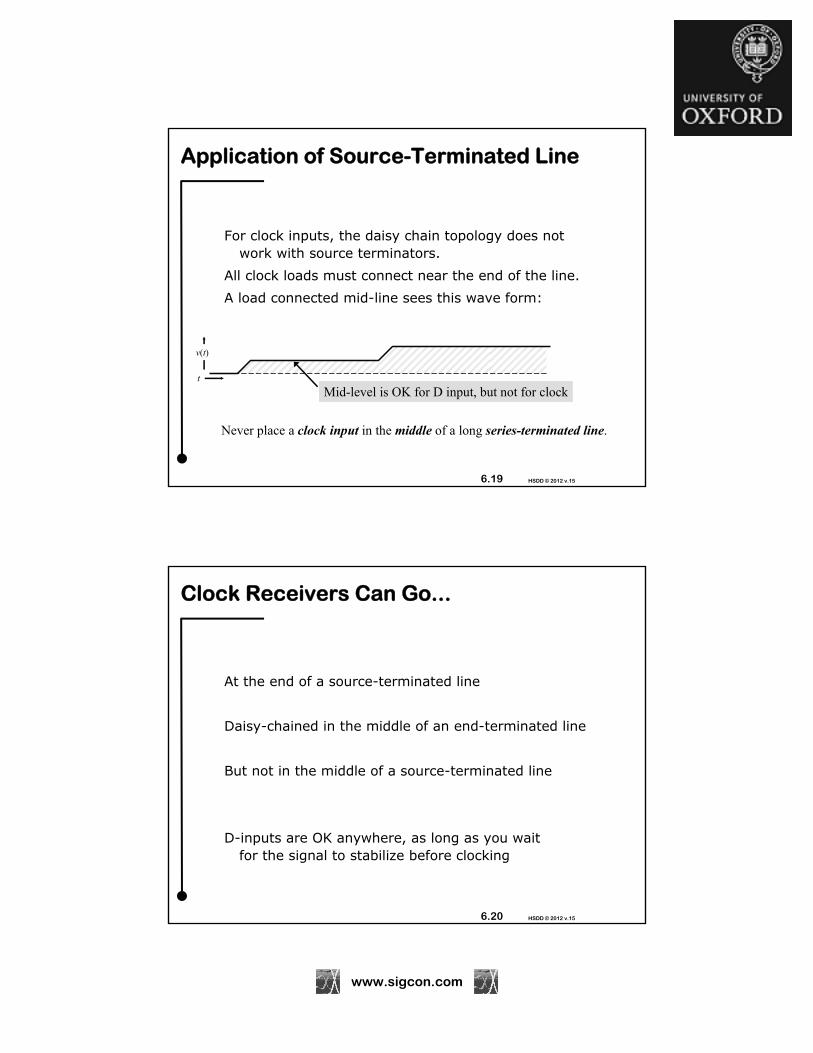
www.sigcon.com
6.19 HSDD © 2012 v.15
Application of Source-Terminated Line
For clock inputs, the daisy chain topology does not work with source terminators.
All clock loads must connect near the end of the line.
A load connected mid-line sees this wave form:
Mid-level is OK for D input, but not for clock
Never place a clock input in the middle of a long series-terminated line.
t
v(t)
6.20 HSDD © 2012 v.15
Clock Receivers Can Go...
At the end of a source-terminated line
Daisy-chained in the middle of an end-terminated line
But not in the middle of a source-terminated line
D-inputs are OK anywhere, as long as you wait for the signal to stabilize before clocking
www.sigcon.com
6.21 HSDD © 2012 v.15
What's That Plateau?
CPU
DRAM
Plateau
3"
6.22 HSDD © 2012 v.15
The Signal at the Bitter End of the Line Might Be OK
Voltage waveforms for an ideal, series-terminated configuration always display beautiful, flat plateaus.
CPU
DRAM
3"
50
1"
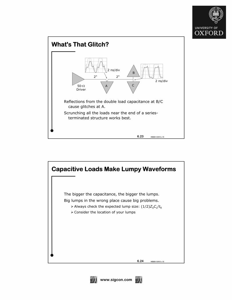
www.sigcon.com
6.23 HSDD © 2012 v.15
What's That Glitch?
Reflections from the double load capacitance at B/C cause glitches at A.
Scrunching all the loads near the end of a series-terminated structure works best.
2" 2"
A
B
C50-Driver
2 ns/div
2 ns/div
6.24 HSDD © 2012 v.15
Capacitive Loads Make Lumpy Waveforms
The bigger the capacitance, the bigger the lumps.
Big lumps in the wrong place cause big problems.
Always check the expected lump size: (1/2)Z0CL/tR
Consider the location of your lumps
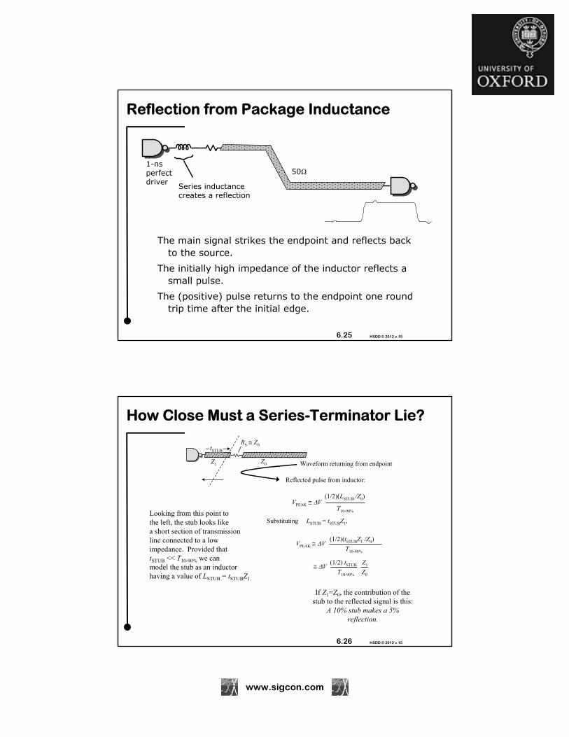
www.sigcon.com
6.25 HSDD © 2012 v.15
Reflection from Package Inductance
The main signal strikes the endpoint and reflects back to the source.
The initially high impedance of the inductor reflects a small pulse.
The (positive) pulse returns to the endpoint one round trip time after the initial edge.
50Ω1-nsperfect driver
Series inductance creates a reflection
6.26 HSDD © 2012 v.15
How Close Must a Series-Terminator Lie?
VPEAK V(1/2)(LSTUB /Z0)
T10-90%
tSTUB
Looking from this point to the left, the stub looks likea short section of transmissionline connected to a lowimpedance. Provided that tSTUB << T10-90% we canmodel the stub as an inductorhaving a value of LSTUB = tSTUBZ1.
Z1 Z0
RS Z0
Reflected pulse from inductor:
Substituting LSTUB = tSTUBZ1,
VPEAK V(1/2)(tSTUBZ1 /Z0)
T10-90%
If Z1=Z0, the contribution of the stub to the reflected signal is this:
A 10% stub makes a 5% reflection.
Waveform returning from endpoint
V(1/2) tSTUB Z1
T10-90% Z0

www.sigcon.com
6.27 HSDD © 2012 v.15
Points to Remember
A series-terminated structure displays a beautiful plateau.
De-rate the ideal source termination value by the output resistance of your driver.
Do NOT place clock receivers in the middle of a long source-terminated line.
6.28 HSDD © 2012 v.15
Both Ends Termination
Combination of end termination also used with series termination.
Used in critical timing applications where even small percentage reflections are intolerable.
Received amplitude is cut in half.
Terminating both ends wastes a lot of power.
Half-sized signal createdby source termination
End termination of Z0
Very little signal bounces off far end
Even less signal bounces a second time Practically nothing
survives first round trip
VCC VCCA=1/2 T=1 Only a half-sized signalmakes it through to the receiver
Z0

www.sigcon.com
6.29 HSDD © 2012 v.15
Comparison of Termination Styles
End termination (a.k.a. split termination)
Series termination
AC termination
Z0
VCC VCC
Z0
Z0
VCC
VCCVCC
VCC
6.30 HSDD © 2012 v.15
End Termination
Termination damps ringing
Signal looks good at any point
First incident wave meets VOH and VOL
+/- 30 mA drive required
Time, ns
Volts
mA
3.3-volt logic, 30-mA driver, 1-ns rise/fall,2-ns line, 50-Ω
source end
far end
(VOH-VT)/Z0 = 30mA

www.sigcon.com
6.31 HSDD © 2012 v.15
Series Termination
Termination damps ringing
Signal appears correct only at far end
Maximum delay is at source
When driving a CMOS input, VOH and VOL are ideal
Current drops to zero after first roundtrip
+/- 30 mA drive required
Time, ns
Volts
mA
3.3-volt logic, 30-mA driver, 2-ns line, 50- Ω
A B
A
B
(VOH/2)/Z0 = 30mA
VOH VCC
6.32 HSDD © 2012 v.15
AC Termination
Termination too weak to dampen ringing
Signal displays overshoot and ringing
Time, ns
Volts
mA
3.3-volt logic, 30-mA driver, 2-ns line, 50- ΩTry zero to 30 pF
0 pF
30 pF
R = 50
C
Z0 = 50T10-90% = 1 ns
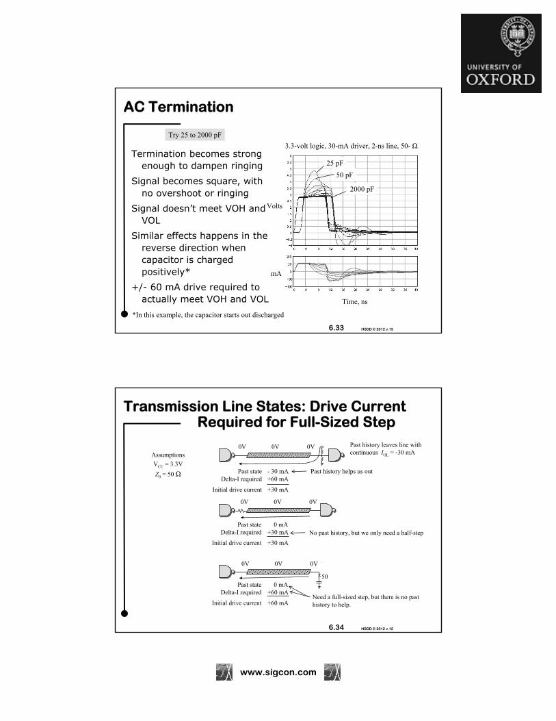
www.sigcon.com
6.33 HSDD © 2012 v.15
AC Termination
Termination becomes strong enough to dampen ringing
Signal becomes square, with no overshoot or ringing
Signal doesn’t meet VOH and VOL
Similar effects happens in the reverse direction when capacitor is charged positively*
+/- 60 mA drive required to actually meet VOH and VOL Time, ns
Volts
mA
3.3-volt logic, 30-mA driver, 2-ns line, 50- Ω
Try 25 to 2000 pF
*In this example, the capacitor starts out discharged
25 pF
50 pF
2000 pF
6.34 HSDD © 2012 v.15
Transmission Line States: Drive Current Required for Full-Sized Step
50
0V 0V 0V
0V 0V 0V
0V 0V 0V
- 30 mA+60 mA
+30 mA
0 mA+30 mA
+30 mA
0 mA+60 mA
+60 mA
Past stateDelta-I required
Initial drive current
Past stateDelta-I required
Initial drive current
Past stateDelta-I required
Initial drive current
Past history helps us out
Need a full-sized step, but there is no pasthistory to help.
No past history, but we only need a half-step
Assumptions
VCC = 3.3V
Z0 = 50 Ω
Past history leaves line with continuous IOL = -30 mA
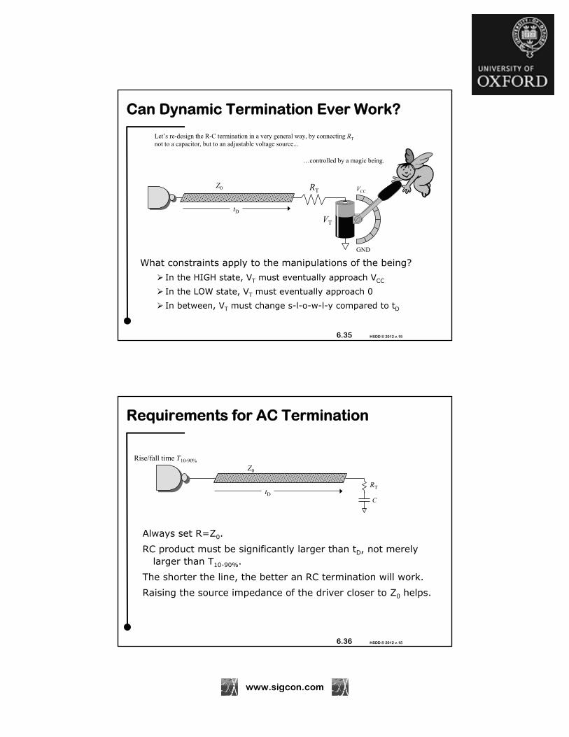
www.sigcon.com
6.35 HSDD © 2012 v.15
RT
VT
Can Dynamic Termination Ever Work?
What constraints apply to the manipulations of the being?
In the HIGH state, VT must eventually approach VCC
In the LOW state, VT must eventually approach 0
In between, VT must change s-l-o-w-l-y compared to tD
Z0
tD
Let’s re-design the R-C termination in a very general way, by connecting RT
not to a capacitor, but to an adjustable voltage source...
…controlled by a magic being.
VCC
GND
6.36 HSDD © 2012 v.15
Requirements for AC Termination
Always set R=Z0.
RC product must be significantly larger than tD, not merely larger than T10-90%.
The shorter the line, the better an RC termination will work.
Raising the source impedance of the driver closer to Z0 helps.
RT
Z0
tD
Rise/fall time T10-90%
C

www.sigcon.com
6.37 HSDD © 2012 v.15
AC Terminator on Short Line (1/2 ns)
We begin with a moderate ringing problem:
T10-90%/tD = (1000 ps)/(500 ps) = 2.0
Add to that an RC time constant that’s significant compared to tD:
RC/tD = (25 pF)(50)/500 ps = 2.5
Signal overshoot improves
Signal meets VOH and VOL at receiver
Driver output current rises modestly, but still enjoys periods of rest.
0 4 8 12 16 20 24 28 32 36 401
0.5
0
0.5
1
1.5
2
2.5
3
3.5
4
4.5
5
5.5
6
0 4 8 12 16 20 24 28 32 36 40100
50
0
50
100
Time, ns
Volts
mA
3.3-volt logic, 30-mA driver, 0.5-ns line, 50- Ω
No termination With AC terminationC = 25 pF
At source
At receiver
6.38 HSDD © 2012 v.15
General Difficulty of Ringing Problem
tD /T10-90% Ringing Solution for first-incident wave switching
2 Full-sized, maximal ringing*
Resistive termination
1 Full-sized, maximal ringing*
Resistive termination
1/2 Slightly attenuated
1/3 Substantially abated
Anything dissipative helps (resistors, diodes, R-C, skin effect, dielectric loss, etc.)
1/6 Almost gone Not necessary
*Maximal as determined by driver source impedance RS and characteristic impedance of line Z0.Relative overshoot on first edge is (Z0-RS)/(Z0+RS).
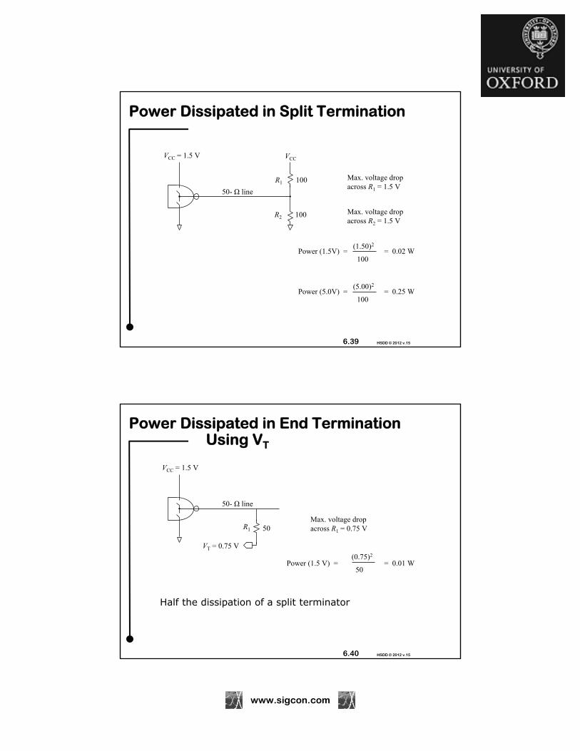
www.sigcon.com
6.39 HSDD © 2012 v.15
Power Dissipated in Split Termination
VCC = 1.5 V
R2
R1Max. voltage dropacross R1 = 1.5 V
Max. voltage dropacross R2 = 1.5 V
50- Ω line
Power (1.5V) = (1.50)2
100= 0.02 W
VCC
100
100
Power (5.0V) = (5.00)2
100= 0.25 W
6.40 HSDD © 2012 v.15
Power Dissipated in End Termination Using VT
Half the dissipation of a split terminator
VCC = 1.5 V
R1
Max. voltage dropacross R1 = 0.75 V
50- Ω line
Power (1.5 V) = (0.75)2
50= 0.01 W
VT = 0.75 V
50
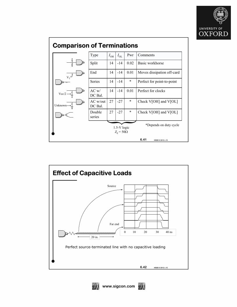
www.sigcon.com
6.41 HSDD © 2012 v.15
Comparison of Terminations
VT
Vcc/2
Unknown
*Depends on duty cycle1.5-V logicZ0 = 50
Basic workhorse0.02-1414Split
CommentsPwrIOLIOHType
Moves dissipation off-card0.01-1414End
Perfect for point-to-point*-1414Series
Perfect for clocks0.01-1414AC w/ DC Bal.
Check V[OH] and V[OL] *-2727AC w/out DC Bal.
Check V[OH] and V[OL] *-2727Double series
6.42 HSDD © 2012 v.15
Effect of Capacitive Loads
Perfect source-terminated line with no capacitive loading
0 10 20 30 40 ns
Source
Far end
20 in.

www.sigcon.com
6.43 HSDD © 2012 v.15
0 1108
2108
3108
4108
0 10 20 30 40 ns
Add One Load in Middle of Line
Every load generates a reflection.
ReflectedFraction =
Edge A hits the capacitor from the left, generating a reflection that bounces back to the source and is absorbed at the driver.
Later, edge B hits the capacitor from the right, generating the reflected blip C.
5-pF
A
B
C
1 Z0 * C2 T10-90%
= 17%
Z0 = 70ΩTDLY = 3.5 nsT10-90% = 1 ns
6.44 HSDD © 2012 v.15
Convert to End-Terminated Line
End termination doesn’t much change the reflected amplitude.
Edge A hits the capacitor, generating a reflected blip that bounces back towards the source.
The blip arrives at the source at B, where it reverses direction, and proceeds to the far end at point C.
0 1108
2108
3108
4108
0 10 20 30 40 ns
70 Ω
5-pF
A
B
C

www.sigcon.com
6.45 HSDD © 2012 v.15
Add More Loads
We have placed the loads uniformly, and spaced within a risetime of each other.
Interestingly, it doesn’t get that much worse.
0 1108
2108
3108
4108
0 10 20 30 40 ns
70 Ω
5-pF each load
6.46 HSDD © 2012 v.15
Wrong termination
Slow Down the Risetime
Slowing down the risetime by a factor of two cuts the bump height in half.
Note that at end of line, the system appears improperly terminated.
Loaded line impedance is:
0 1108
2108
3108
4108
0 10 20 30 40 ns
70 Ω
5-pF each load
2-ns risetime
ZLOADED = Z0 = 57 CLINE
CLOAD + CLINE
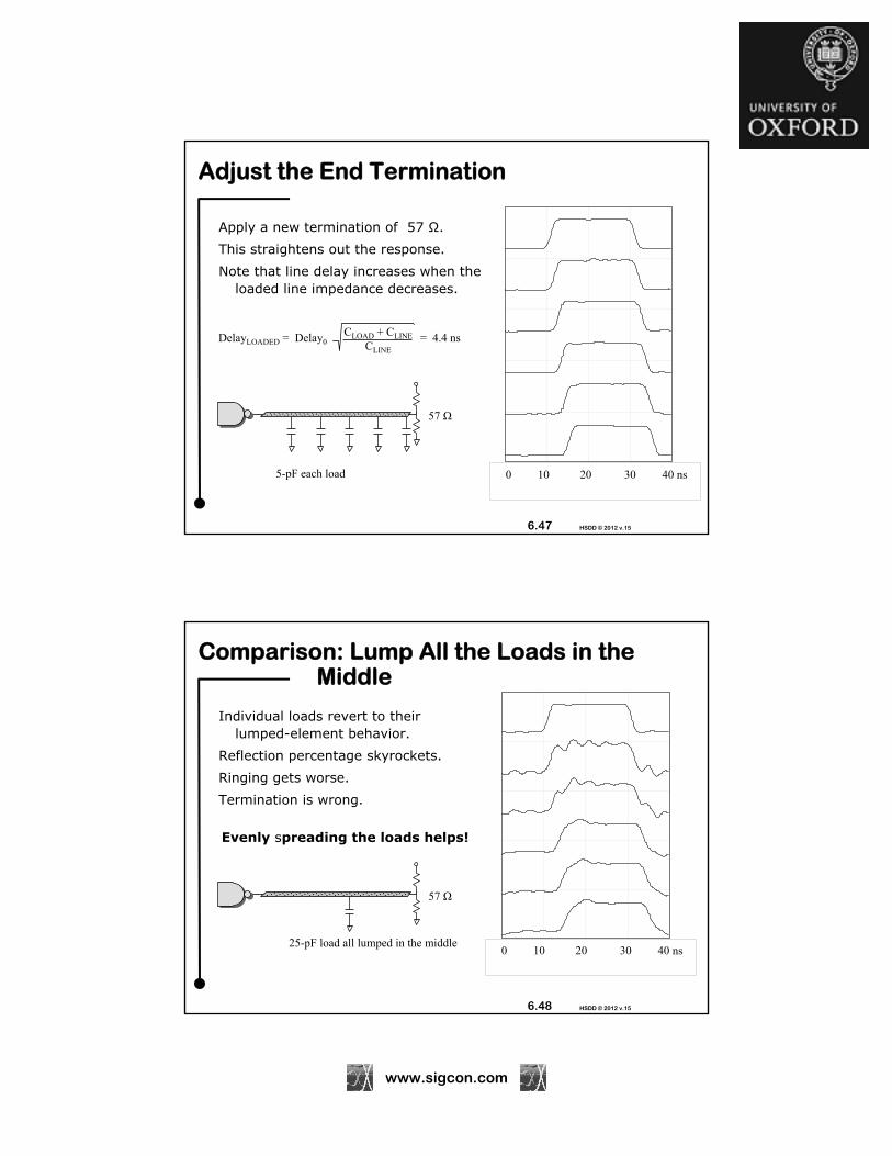
www.sigcon.com
6.47 HSDD © 2012 v.15
Adjust the End Termination
Apply a new termination of 57 Ω.
This straightens out the response.
Note that line delay increases when the loaded line impedance decreases.
57 Ω
5-pF each load
DelayLOADED = Delay0 = 4.4 ns CLOAD + CLINE
CLINE
0 1108
2108
3108
4108
0 10 20 30 40 ns
6.48 HSDD © 2012 v.15
Comparison: Lump All the Loads in the Middle
Individual loads revert to their lumped-element behavior.
Reflection percentage skyrockets.
Ringing gets worse.
Termination is wrong.
0 1108
2108
3108
4108
0 10 20 30 40 ns
57 Ω
25-pF load all lumped in the middle
Evenly spreading the loads helps!

www.sigcon.com
6.49 HSDD © 2012 v.15
Key Equations
The loaded impedance of the bus is less than Z0
Basic line parameters (whole-line values or per-section values)
The loaded delay of the bus is greater than the initial delay tD
Adding capacitance reduces ZL
…and increases tLOADED
D 0 0t L C D0
0
tC
Z
0 D 0L t Z
0LOADED 0
0 L
CZ Z
C C
0 LLOADED D
0
C Ct t
C
6.50 HSDD © 2012 v.15
Heavily-Loaded Bus Design
0.5"
Z0=50
0
0
0.5 in. 180 ps/in.1.8 pF
50
delayC
Z
0 0 0.5 in. 180 ps/in. 50 4500 pHL delay Z
L 5.5 pFC
0
LOADED0 L
4500 pH24.8 Ω
1.8 5.5 pF
LZ
C C
(Values calculated on a per-load basis)

www.sigcon.com
6.51 HSDD © 2012 v.15
Idea for Design
Stagger the loads on a bus for better signal quality.
This layout has twice as many loads, eachwith half the CL, and half the spacing.
Looks good on layout,but doesn’t perform as well.
DSP DSP DSP
DSPDSP DSPT
ER
M
TE
RM
DSP
DSP
DSP
DSP
DSP
DSP
TE
RM
TE
RM
6.52 HSDD © 2012 v.15
Points to Remember
Capacitive loads cause reflections
If evenly spread, we can counteract the effect of capacitive loading
Evenly-spaced capacitive loads decrease line impedance, and increase delay
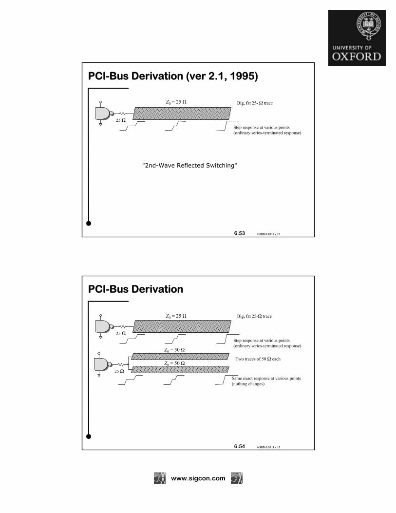
www.sigcon.com
6.53 HSDD © 2012 v.15
PCI-Bus Derivation (ver 2.1, 1995)
25 Ω
Z0 = 25 Ω Big, fat 25- Ω trace
Step response at various points(ordinary series-terminated response)
"2nd-Wave Reflected Switching"
6.54 HSDD © 2012 v.15
PCI-Bus Derivation
25 Ω
Z0 = 25 Ω Big, fat 25-Ω trace
Step response at various points(ordinary series-terminated response)
25 Ω
Z0 = 50 Ω
Two traces of 50 Ω each
Same exact response at various points(nothing changes)
Z0 = 50 Ω
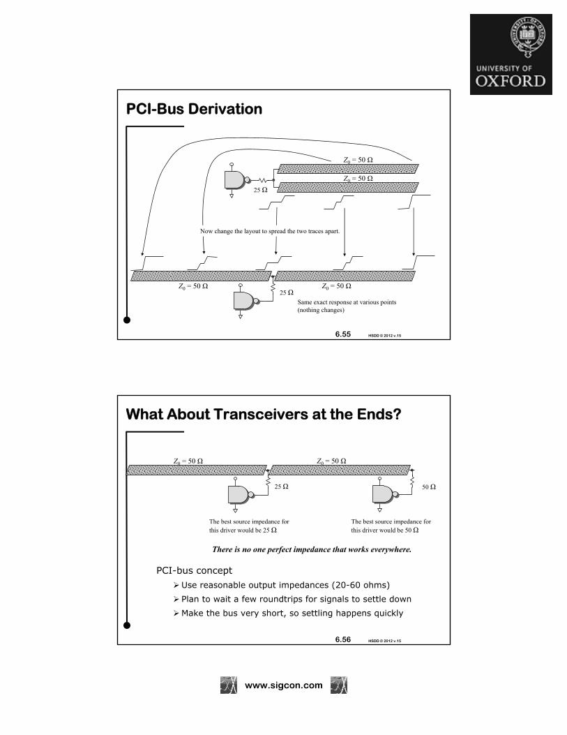
www.sigcon.com
6.55 HSDD © 2012 v.15
PCI-Bus Derivation
25 Ω
Z0 = 50 Ω
Z0 = 50 Ω
25 ΩZ0 = 50 Ω
Same exact response at various points(nothing changes)
Z0 = 50 Ω
Now change the layout to spread the two traces apart.
6.56 HSDD © 2012 v.15
What About Transceivers at the Ends?
PCI-bus concept
Use reasonable output impedances (20-60 ohms)
Plan to wait a few roundtrips for signals to settle down
Make the bus very short, so settling happens quickly
25 Ω
Z0 = 50 Ω
The best source impedance for this driver would be 50 Ω
Z0 = 50 Ω
50 Ω
There is no one perfect impedance that works everywhere.
The best source impedance for this driver would be 25 Ω

www.sigcon.com
6.57 HSDD © 2012 v.15
Circle Bus
Good for embedded multi-processors.
Everybody thinks they are in the middle.
RS should ideally equal Z0/2, where Z0 is the loaded impedance of the structure.
25 Ω
Z0 = 50 Ω
25 Ω
25 Ω
25 Ω25 Ω
Equally space the loadsaround the ring.
RS
May be covered by U.S. pat. 5,146,634
25 Ω
6.58 HSDD © 2012 v.15
Extra for Experts
Multiple Loads Clumped at End of Series-term Line
Bi-Directional Termination
Risetime with Capacitive Load
Effect of Inductive Bead on Risetime
Diode Termination
The Weak End-Termination
Differential Terminations
Effect of Tightly Coupling the Differential Pair
Right-Angle Bends
Via Reflections
Reflections from Taps
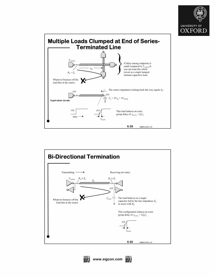
www.sigcon.com
6.59 HSDD © 2012 v.15
Multiple Loads Clumped at End of Series-Terminated Line
If delay among endpoints is small compared to T10-90%/6, you can treat this whole circuit as a single lumped-element capacitive load.
tD
T10-90%
RS = Z0
CL = 3CIN + 3CSTUB
The source impedance looking back this way equals Z0.
This load induces an extra group delay of 0-63% = Z0CL
0-63%
time
x(t)y(t)
x(t) y(t)
Whatever bounces off the load dies at the source
Equivalent circuit:
6.60 HSDD © 2012 v.15
Bi-Directional Termination
T10-90%
Whatever bounces off the load dies at the source
The load behaves as a single capacitor fed by the line impedance Z0
in series with RS.
Transmitting Receiving (tri-state)
Z0
RS Z0 RS Z0
This configuration induces an extra group delay of 0-63% = 2Z0CL
0-63%
y(t)
y(t)
COUT

www.sigcon.com
6.61 HSDD © 2012 v.15
Risetime with Capacitive Load
T10-90%
RTERM Z0
Z0
The load behaves as a single capacitor fed by the line impedance Z0
in parallel with RTERM.
This configuration induces an extra group delay of 0-63% = (1/2)Z0CL , plus extra reflections that re-appear after time 2tD
Termination 0-63%
Bi-directional 2Z0COUT
Series-term Z0CL
End-term ½ Z0CIN
0-63%
y(t)
y(t)tD
6.62 HSDD © 2012 v.15
Effect of Inductive Bead on Risetime
To generate a specific time constant 0-63% using an inductive bead,
Let f = 1/(20-63%)
Pick bead such that the bead impedance Z(f) equals Z0 at frequency f.
The load impedance lookingthis way equals Z0.
x(t)
0-63%
y(t)
y(t) The inductor introduces an extra group delay of 0-63% = (L/Z0) in the initial launched waveform.
The 10-90% risetime of the initially-launched waveform is approximately: TLAUNCHED = (T10-90%
2 + (2.20-63%)2)1/2
T10-90%

www.sigcon.com
6.63 HSDD © 2012 v.15
Diode Termination
The diode clamps prevent overshoot if and only if, The driver output is full-sized (RS << Z0)
The diodes clamp quickly (tON, tOFF << T10-90%)
To the correct voltage (diode Vf << VCC)
With low enough impedance (diode area is HUGE)
And the load capacitance is insignificant (Z0CIN << T10-90%)
If all conditions are satisfied, The diodes clamp perfectly
There is no overshoot
The received voltage equals the transmitted voltage (T = 1)
No reflections ensue (p2 = 0)
Large currents persist on the line (IOH(t0) = V/Z0)
T10-90%VCC
Z0 y(t)
tD
2 = T - 1 T = 1 + 2
CIN
Diodes and other non-linear active terminations only work for relatively short lines.
6.64 HSDD © 2012 v.15
Diode Termination Examples
Each figure compares three different terminations styles:
None (open-circuited at endpoint)
Diode termination (Schottky diodes, 5-ohm RON, Cp=3 pF)
Series termination (perfect 65- source)
0V
3V
2 ns/div
0V
3V
2 ns/div
0V
3V
2 ns/div
T10-90% = 1 ns
Z0 = 65 ohms
Driver RS = 23 ohms
NoneDiode
Series
NoneDiode
Series
NoneDiode
Series
2-inch line 4-inch line 8-inch line
Diodes help reduce ringback, andDiodes dissipate very little power, butThey aren’t perfect.

www.sigcon.com
6.65 HSDD © 2012 v.15
The Weak End-Termination
2:1 termination mis-match results in 10 dB reflection loss per round trip
1/2 the power dissipation of a regular end termination
Signal isn’t perfect, but it’s better than nothing
First incident edge still doesn’t meet VOH and VOL , but it’s closer
+/- 45 mA drive required to actually meet VOH and VOL
Time, ns
Volts
mA
3.3-volt logic, 30-mA driver, 2-ns line, 50- Ω
Try 100-Ω end termination (200/200)
6.66 HSDD © 2012 v.15
Z0
Connects to reference plane usedby traces.
+-
2Z0 +-
This circuit terminates both differential and common-mode signals (like intra-pair skew). Use it when you have a low-impedance driver on a long line, with no other attempt made to dampen common-mode resonances:
Z0
End Termination of Differential-Mode Signals
This circuit terminates only the differential mode, not the common mode. Use it when your driver has a moderate output impedance, something that can partly damp common-mode resonance:

www.sigcon.com
6.67 HSDD © 2012 v.15
Differential Termination with Re-Biasing
RT = Z0
+-
RT = Z0
This circuit does the job...
...But this one introduces less DC offset.
Z0
+-
Z0
Connect tosource of bias voltage
Either circuit can accept DC-blocking capacitors for DC-level adjustment of DC-balanced signals (like clocks, Manchester
coding, 8B10B coding, etc.) .
6.68 HSDD © 2012 v.15
Effect Of Tightly Coupling the Differential Pair
Routing the two elements of a differential pair extraordinarily close together has these effects:
Lowers the differential impedance (you have to make the lines extra-skinny to correct the impedance).
Raises skin-effect losses (because the traces are now skinnier).
Pisses off your layout people (because now the pair can’t be split to traverse obstacles).
Contrary to what you may hear, it doesn’t improve EMI, because it is mostly the common-mode signals from your drivers (the natural imbalance, the skew, etc.) that radiate.
Permits somewhat better pair-to-pair pitch, due to slightly lowered crosstalk. This is the only good reason for using tightly-coupled traces.

www.sigcon.com
6.69 HSDD © 2012 v.15
Right Angle Bends
Here’s a theme I hear all the time.
Usually it comes from a layout person who has worked on ECL systems.
Right angle bends slow down fast signals
Right angle bends cause reflections
You have to avoid right angle bends or the signal will jump right off the trace and propagate into space, just like an antenna
Is it true?
6.70 HSDD © 2012 v.15
Stories About Right Angle Bends Have a Basis in Fact
w
w
Effective widthat corner is too large
w
Nominalwidth
The shaded areaacts like an extra capacitanceconnectedto the line
The additional capacitance in the shaded area is approximately:
The peak value of the signal reflected from a capacitive load is:
Example: w = .010 in.er = 4.3Z0 = 50 ΩC = 0.025 pFT10-90 = 1 nsV = 3.3 V (amplitude of incoming step)VPEAK = 0.0021 V
Nominalwidth
61 w er1/2
Z0
C = pF1 Z0 * C2 T10-90%
VPEAK = V

www.sigcon.com
6.71 HSDD © 2012 v.15
What About the Right-Angle Bend Going Down Into a Via?
The right-angle bend doesn’t do anything, but the parasitic capacitance between the via to ground does, and so does the temporary separation of signal and return paths.
Overall height.063 in.
Clearance hole Solid ground plane
Pad .028 in.
Body of via .016 in.
.050 in.
A
Your signal goes rightdown the hole
6.72 HSDD © 2012 v.15
Via Reflections
The capacitance of a .028-pad via is on the order of 1/2 pF to 1 pF, depending on the board construction and ground plane configuration
C = 1 pF
The peak value of the signal reflected from a capacitive load is:
Example: Z0 = 70 ΩT10-90% = 1 ns = 3.5 % (small, but noticeable)
Signal vias that traverse multiple planes are subject to additional inductive effects due to the temporary separation of signal and return paths.
1 Z0 * C2 T10-90%
VPEAK = V
VPEAK
V
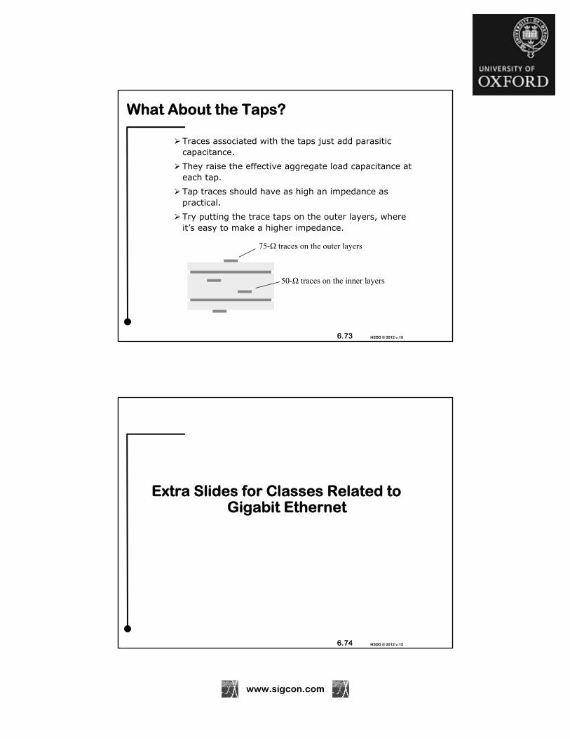
www.sigcon.com
6.73 HSDD © 2012 v.15
What About the Taps?
Traces associated with the taps just add parasitic capacitance.
They raise the effective aggregate load capacitance at each tap.
Tap traces should have as high an impedance as practical.
Try putting the trace taps on the outer layers, where it’s easy to make a higher impedance.
75-Ω traces on the outer layers
50-Ω traces on the inner layers
6.74 HSDD © 2012 v.15
Extra Slides for Classes Related toGigabit Ethernet

www.sigcon.com
6.75 HSDD © 2012 v.15
Serial Interface (1.25 Gb/s)
ZTERM
Z0 = 75ΩS
ecti
on 1
Sec
tion
2
Sec
tion
3
Sec
tion
4
Vias will be added here and here
The simulation models four sections of balanced, 150-ohm transmission line.
2” 2” 2” 2”
Z0 = 75Ω
ZSOURCE
This example demonstrates theefficacy of both-ends termination.
6.76 HSDD © 2012 v.15
Perfect Line: Both Ends Terminated
Len
gth
Z0
Ser
ies-
L (
nH)
Shun
t-C
(pF
)
section 1section 2section 3section 4
0 0.5 1 1.5 21.5
1
0.5
0
0.5
1
1.5Eye pattern
params
2
2
2
2
75
75
75
75
0
0
0
0
0
0
0
0
=
ZSOURCE 0( ) 75=
ZTERM 0( ) 75=
0 0.2 0.4 0.6 0.8 1 1.2 1.4 1.6 1.8 2 2.2 2.4 2.6 2.8 3 3.2 3.4 3.6 3.8 41.5
1
0.5
0
0.5
1
1.5
Signal at end of line

www.sigcon.com
6.77 HSDD © 2012 v.15
With Dielectric Loss
8-inch lineTan =0.02
0 0.5 1 1.5 21.5
1
0.5
0
0.5
1
1.5Eye pattern
params
2
2
2
2
75
75
75
75
0
0
0
0
0
0
0
0
=
ZSOURCE 0( ) 75=
ZTERM 0( ) 75=
0 0.2 0.4 0.6 0.8 1 1.2 1.4 1.6 1.8 2 2.2 2.4 2.6 2.8 3 3.2 3.4 3.6 3.8 41.5
1
0.5
0
0.5
1
1.5
Signal at end of line
F0 0.02
Re R SKIN 2j 109
0
6.78 HSDD © 2012 v.15
With Skin Effect
RSKIN = 1.00 Ω/inchAt 1 GHz
0 0.5 1 1.5 21.5
1
0.5
0
0.5
1
1.5Eye pattern
F0 0.02
Re R SKIN 2j 109
1
params
2
2
2
2
75
75
75
75
0
0
0
0
0
0
0
0
ZSOURCE 0( ) 75
ZTERM 0( ) 75
0 0.2 0.4 0.6 0.8 1 1.2 1.4 1.6 1.8 2 2.2 2.4 2.6 2.8 3 3.2 3.4 3.6 3.8 41.5
1
0.5
0
0.5
1
1.5
Signal at end of line

www.sigcon.com
6.79 HSDD © 2012 v.15
Add Some Termination Mismatch
ZS = 60ZL = 60Z0 = 75
0 0.5 1 1.5 21.5
1
0.5
0
0.5
1
1.5Eye pattern
ZSOURCE 0( ) 60
ZTERM 0( ) 60
0 0.2 0.4 0.6 0.8 1 1.2 1.4 1.6 1.8 2 2.2 2.4 2.6 2.8 3 3.2 3.4 3.6 3.8 41.5
1
0.5
0
0.5
1
1.5
Signal at end of line
F0 0.02
Re R SKIN 2j 109
1
params
2
2
2
2
75
75
75
75
0
0
0
0
0
0
0
0
6.80 HSDD © 2012 v.15
Add Two Small Vias
0 0.5 1 1.5 21.5
1
0.5
0
0.5
1
1.5Eye pattern
ZSOURCE 0( ) 60
ZTERM 0( ) 60
0 0.2 0.4 0.6 0.8 1 1.2 1.4 1.6 1.8 2 2.2 2.4 2.6 2.8 3 3.2 3.4 3.6 3.8 41.5
1
0.5
0
0.5
1
1.5
Signal at end of line Two vias,1-pF each,located 4” and 6”
from source
F0 0.02
Re R SKIN 2j 109
1
params
2
2
2
2
75
75
75
75
0
0
0
0
0
1
1
0

www.sigcon.com
6.81 HSDD © 2012 v.15
Add Receiver Load
0 0.5 1 1.5 21.5
1
0.5
0
0.5
1
1.5Eye pattern
0 0.2 0.4 0.6 0.8 1 1.2 1.4 1.6 1.8 2 2.2 2.4 2.6 2.8 3 3.2 3.4 3.6 3.8 41.5
1
0.5
0
0.5
1
1.5
Signal at end of line Additional3-pF at receiver
ZSOURCE 0( ) 60
ZTERM 0( ) 60
F0 0.02
Re R SKIN 2j 109
1
params
2
2
2
2
75
75
75
75
0
0
0
0
0
1
1
3
6.82 HSDD © 2012 v.15
Convert to Termination at End Only
0 0.5 1 1.5 21.5
1
0.5
0
0.5
1
1.5Eye pattern
ZSOURCE 0( ) 10
ZTERM 0( ) 60
0 0.2 0.4 0.6 0.8 1 1.2 1.4 1.6 1.8 2 2.2 2.4 2.6 2.8 3 3.2 3.4 3.6 3.8 41.5
1
0.5
0
0.5
1
1.5
Signal at end of lineSource impedance=10 ohms
F0 0.02
Re R SKIN 2j 109
1
params
2
2
2
2
75
75
75
75
0
0
0
0
0
1
1
3

!!!"#$%&'("&')

www.sigcon.com
HSDD © 2012 v.15
Other Courses by Dr. Howard Johnson
Private classes available
www.sigcon.com
ADVANCED HIGH-SPEEDSIGNAL PROPAGATION
Press your design to the upper limits of speed and distance
HIGH-SPEEDNOISE AND GROUNDING
Master the art of mixed-signal system design
HSDD © 2012 v.15
Chapter 8: Rock-Solid Power
Performance of individual capacitors
Arrays of capacitors

www.sigcon.com
8.3 HSDD © 2012 v.15
The Four Parts of a Power System
VRM and its connector/wiring
Bulk decoupling capacitor
Bypass capacitor array
VCC-GND plane-to-plane capacitance
PLAY MOVIE WM9
8.4 HSDD © 2012 v.15
Electrical Model of Capacitor
As long as you stay below the maximum voltage rating, a capacitor behaves much like an L-R-C series resonant circuit.
Parasitic series inductance(ESL)
Parasitic series resistance (ESR)
Sensitivity toTemperature
& AgeMaximum voltage rating
(DCWV)
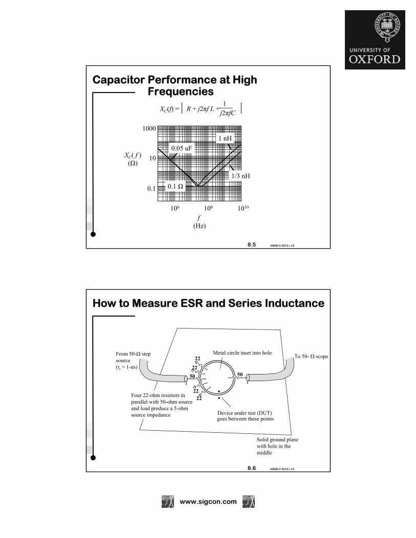
www.sigcon.com
8.5 HSDD © 2012 v.15
Capacitor Performance at High Frequencies
XC(f) = | R + j2πf L + |1j2πfC
XC( f )(Ω)
f (Hz)
1000
0.1
10
106 108 1010
0.1 Ω
0.05 uF
1 nH
1/3 nH
8.6 HSDD © 2012 v.15
Four 22-ohm resistors in parallel with 50-ohm source and load produce a 5-ohm source impedance
How to Measure ESR and Series Inductance
Device under test (DUT)goes between these points
Solid ground plane with hole in the middle
From 50-Ω stepsource(tr = 1-ns)
To 50- Ω scope
50
2222
22
2250
Metal circle inset into hole

www.sigcon.com
8.7 HSDD © 2012 v.15
Thevenin Equivalent for Test Circuit
+-
+
-
5.0 Ω
t10-90 = 1.0 ns
100 mVstep
y(t)
D.U.T. goes here
8.8 HSDD © 2012 v.15
You Might Expect
y(t)
Voltage asymptotically approachesfull output level
t0-63% = RSCL
Let’s zoom in on just this little partright at the beginning
Let RS be the tester source impedance, andCL be the D.U.T. capacitance
t
www.sigcon.com
8.9 HSDD © 2012 v.15
Measured Results
figure 8.11 2 nS/div
OpenCircuit
Capacitorresponse
Open circuit (1)
Capacitor response (2)
Spike Step Slow ramp
50 mV
50 mV
20 nS/div
8.10 HSDD © 2012 v.15
Three Parts of a Capacitor Step Response
+
+
All three superimposed
together
=
The inductance (ESL) produces a quick pulse
The resistance (ESR) makes a plateau of constant height
The capacitance determines the rate of charge—on a very fast scale of time the slope looks quite shallow
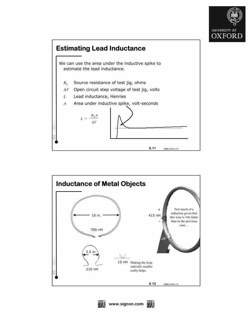
www.sigcon.com
8.11 HSDD © 2012 v.15
Estimating Lead Inductance
We can use the area under the inductive spike to estimate the lead inductance.
RS Source resistance of test jig, ohms
ΔV Open circuit step voltage of test jig, volts
L Lead inductance, Henries
A Area under inductive spike, volt-seconds
L = ΔV
RS A
8.12 HSDD © 2012 v.15
Inductance of Metal Objects
Not much of a reduction given that
this wire is 10x fatter than in the previous
case…
10 in.
700 nH
+
415 nH
–
210 nH
15 nH
3.5 in.
Making the loop radically smaller really helps.

www.sigcon.com
8.13 HSDD © 2012 v.15
Inductance of Leaded Bypass Capacitors
0.01 uF long legs 25.8 nH
0.01 uF short legs 4.6 nH
10 uF electrolytic 1.9 nH
2200 uF electrolytic 9.4 nH
8.14 HSDD © 2012 v.15
Surface-Mounted Configurations
I tried a variety of surface-mounted capacitor layouts at 100:1 physical scale.
0.030 squaresoldering pad
All dimensions in inches
.024 roundvia pad
0603 component
0.050
.0075
0.050
.030
.010 dia.hole
0603 skinny 0603 fat 0603 end
0402 end
0603 side
0402 side
0.020 squaresoldering pad
Same via and hole

www.sigcon.com
8.15 HSDD © 2012 v.15
Inductance of Surface-Mounted Layouts
All inductance values in nH
Hole dia. 0.010 in. Hole dia. 0.020 in.
Via length: .020 .010 .006 .004 .020 .010 .006 .004
0603 skinny 2.87 2.18 1.77 1.51 2.68 2.13 1.66 1.51
0603 fat 2.23 1.52 1.17 0.95 2.07 1.47 1.12 0.89
0603 end 1.16 0.77 0.59 0.50 1.07 0.68 0.53 0.42
0603 side 0.85 0.61 0.46 0.36 0.67 0.51 0.38 0.33
0402 end 1.01 0.67 0.50 0.42 0.82 0.58 0.44 0.38
0402 side 0.60 0.40 0.32 0.26 0.43 0.32 0.25 0.21
8.16 HSDD © 2012 v.15
Points to Remember
ESR acts like a resistor in series with a capacitor
ESL acts like an inductor in series with a capacitor
The inductance is determined by where current flows within the capacitor layout and package
Inductance degrades the performance of a capacitor at high frequencies

www.sigcon.com
8.17 HSDD © 2012 v.15
New Surface-Mounted Packages are Constantly Being Developed
Smaller packages
Try out the new 0402 (and even tinier 0201)
Pad design becomes critical for these tiny parts
Talk to your component vendor
Some companies have developed proprietary pad designs (for example, see Motorola patent U.S. 5,453,581)
Capacitors arrays
0603-size with four capacitors (which you can place in parallel)
(http://www.murata.com)
1206-size with eight capacitors (already wired in parallel)
(http://www.avxcorp.com)
8.18 HSDD © 2012 v.15
AVX Interdigitated Capacitor (IDC)
Alternating solder pads connect to VCC, GND.
Very low-inductance structure.
Intended for BGA applications.
Eight-via footprint:
Gnd
Vcc
+ - + -
+-+-
Gnd
Vcc
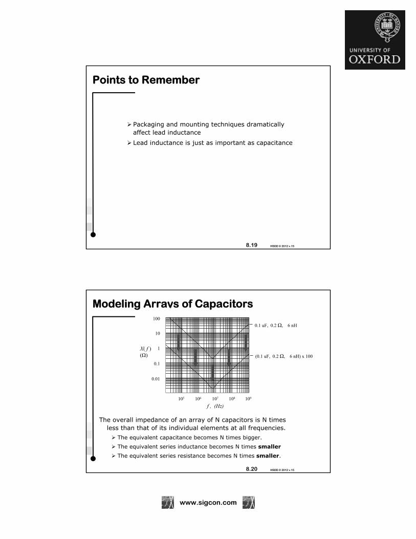
www.sigcon.com
8.19 HSDD © 2012 v.15
Points to Remember
Packaging and mounting techniques dramatically affect lead inductance
Lead inductance is just as important as capacitance
8.20 HSDD © 2012 v.15
Modeling Arrays of Capacitors
The overall impedance of an array of N capacitors is N times less than that of its individual elements at all frequencies.
The equivalent capacitance becomes N times bigger.
The equivalent series inductance becomes N times smaller
The equivalent series resistance becomes N times smaller.
X( f )(Ω)
f , (Hz)
1 104
1 105
1 106
1 107
1 108
1 1090.001
0.01
0.1
1
10
100
0.1 uF, 0.2 Ω, 6 nH
100
0.01
0.1
10
1
105 106 107 108 109
(0.1 uF, 0.2 Ω, 6 nH) x 100
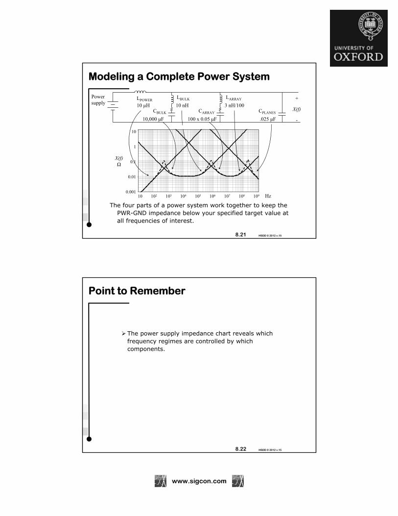
www.sigcon.com
8.21 HSDD © 2012 v.15
10 100 1 103 1 104 1 105 1 106 1 107 1 108 1 1090.001
0.01
0.1
1
10
10 102 103 104 105 106 107 108 109
10
1
0.1
0.01
0.001
Modeling a Complete Power System
The four parts of a power system work together to keep the PWR-GND impedance below your specified target value at all frequencies of interest.
Power supply
X(f)
+
-
CBULK
LBULK
CARRAY
LARRAY
CPLANES
LPOWER
.025 μF10,000 μF 100 x 0.05 μF
3 nH/10010 nH10 μH
X(f)Ω
Hz
8.22 HSDD © 2012 v.15
Point to Remember
The power supply impedance chart reveals which frequency regimes are controlled by which components.

www.sigcon.com
Olde Tyme Use of Dual-Value Capacitor Arrays (1960)
1050.1
1
10
100
1000
106 107 109
f (Hz)
XC(ohms)
In 1960, a big capacitor always had a big series inductance...
Paralleling the two parts delivered the benefit of large capacitance here...
Big cap .1 uF
Small cap .001 uF20 nH
2 nH While a small capacitor had a small inductance
…and small inductance here.
108
8.24 HSDD © 2012 v.15
The Same Approach Today Doesn’t Work
1050.1
1
10
100
1000
106 107 109
f (Hz)
XC
(ohms)
Today all ceramic capacitors in the same package havethe same series inductance, regardless of the capacitance.
Paralleling these two parts delivers only a 6dB improvement at the high end.
Big cap .1 uF
Small cap .001 uF Both in parallel = 1 nH
Each cap. = 2 nH
0.2-ESR
Resonanceeffect

www.sigcon.com
8.25 HSDD © 2012 v.15
10
100
1000
XC
(ohms)
1050.1
1
106 107 108 109
f (Hz)
Just Choose the Smallest Package You Can Manufacture, And Buy the Biggest Value You Can
A better approach, if the capacitors are all in the same package, is to simply use twice as many of the biggest value. This scheme delivers 6 dB across all frequencies, and is simpler to manage.
Big cap.
Small cap.
Two big caps
8.26 HSDD © 2012 v.15
Points To Remember
For bypass applications, use the lowest-inductance (smallest) package you can.
Choose the largest value you can reliably purchase in that package size.