section 4 high speed sampling and high speed adcs, walt …€¦ · 1 section 4 high speed sampling...
TRANSCRIPT
1
SECTION 4HIGH SPEED SAMPLING ANDHIGH SPEED ADCs, Walt Kester
INTRODUCTION
High speed ADCs are used in a wide variety of real-time DSP signal-processingapplications, replacing systems that used analog techniques alone. The major reasonfor using digital signal processing are (1) the cost of DSP processors has gone down,(2) their speed and computational power has increased, and (3) they arereprogrammable, thereby allowing for system performance upgrades withouthardware changes. DSP offers solutions that cannot be achieved in the analogdomain, i.e. V.32 and V.34 modems.
However, in order for digital signal processing techniques to be effective in solvingan analog signal processing problem, appropriate cost effective high speed ADCsmust be available. The ADCs must be tested and specified in such a way that thedesign engineer can relate the ADC performance to specific system requirements,which can be more demanding than if they were used in purely analog signalprocessing systems. In most high speed signal processing applications, ACperformance and wide dynamic range are much more important than traditional DCperformance. This requires that the ADC manufacturer not only design the rightADCs but specify them as completely as possible to cover a wide variety ofapplications.
Another important aspect of integrating ADCs into a high speed system is acomplete understanding of the sampling process and the distortion mechanismswhich ultimately limit system performance. High speed sampling ADCs first wereused in instrumentation and signal processing applications, where much emphasiswas placed on time-domain performance. While this is still important, applicationsof ADCs in communications also require comprehensive frequency-domainspecifications.
Modern IC processes also allow the integration of more analog functionality into theADC, such as on-board references, sample-and-hold amplifiers, PGAs, etc. Thismakes them easier to use in a system by minimizing the amount of support circuitryrequired.
Another driving force in high speed ADC development is the trend toward lowerpower and lower supply voltages. Most high speed sampling ADCs today operate oneither dual or single 5V supplies, and there is increasing interest in single-supplyconverters which will operate on 3V or less for battery powered applications. Lowersupply voltages tend to increase a circuit's sensitivity to power supply noise andground noise, especially mixed-signal devices such as ADCs and DACs.
The trend toward lower cost and lower power has led to the development of a varietyof high speed ADCs fabricated on standard 0.6 micron CMOS processes. Making aprecision ADC on a digital process (no thin film resistors are available) is a realchallenge to the IC circuit designer. ADCs which require the maximum in
2
performance still require a high speed complementary bipolar process (such asAnalog Devices' XFCB) with thin film resistors.
The purpose of this section is to equip the engineer with the proper tools necessaryto understand and select ADCs for high speed systems applications. Makingintelligent tradeoffs in the system design requires a thorough understanding of thefundamental capabilities and limitations of state-of-the-art high speed samplingADCs.
HIGH SPEED SAMPLING ADCs
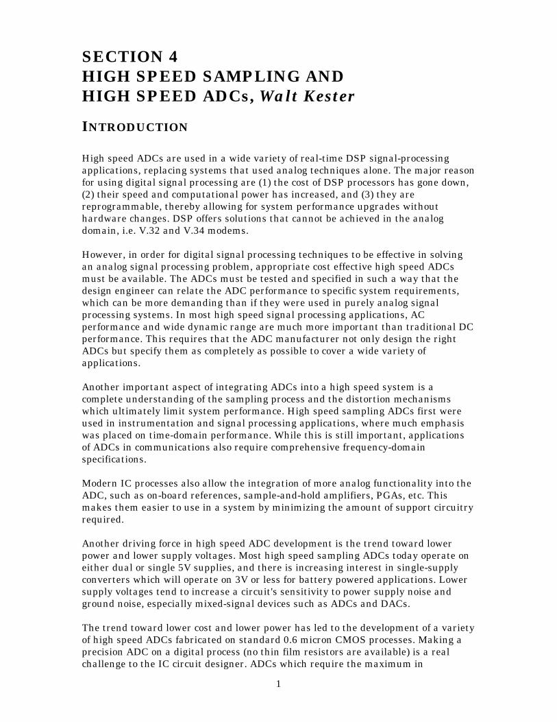
nn Wide Acceptance in Signal Processing and Communications
nn Emphasis on Dynamic Performance
nn Trend to Low Power, Low Voltage, Single-Supply
nn More On-Chip Functionality: PGAs, SHA, Digital Filters, etc.
nn Process Technology:
uu Low Cost CMOS: Up to 12-bits @ 10MSPS
uu High Speed Complementary Bipolar: Up to 12-bits @ 70MSPS
uu Statistical Matching Techniques Rather than Thin FilmLaser Trimming
a 4.1
FUNDAMENTALS OF HIGH SPEED SAMPLING
The sampling process can be discussed from either the frequency or time domain orboth. Frequency-domain analysis is applicable to communications, so that's what wewill consider.
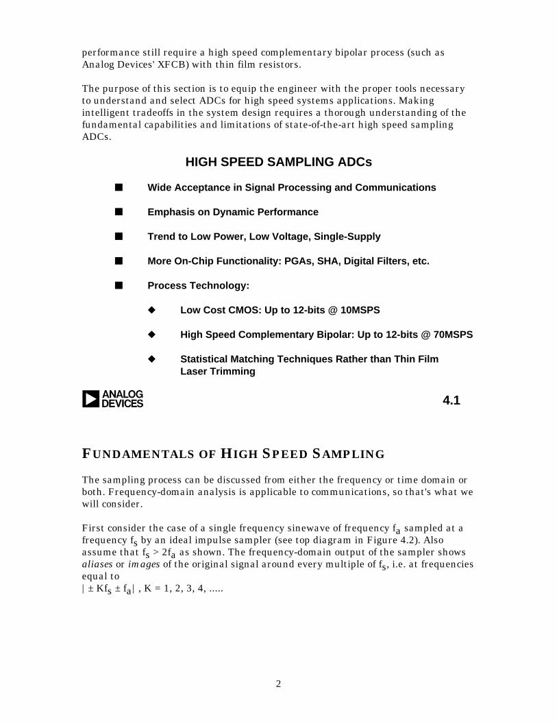
First consider the case of a single frequency sinewave of frequency fa sampled at afrequency fs by an ideal impulse sampler (see top diagram in Figure 4.2). Alsoassume that fs > 2fa as shown. The frequency-domain output of the sampler showsaliases or images of the original signal around every multiple of fs, i.e. at frequenciesequal to|± Kfs ± fa|, K = 1, 2, 3, 4, .....
3
a
ANALOG SIGNAL fa SAMPLED @ fs USING IDEAL SAMPLER
HAS IMAGES (ALIASES) AT |±Kfs ±fa|, K = 1, 2, 3, . . .
4.2
0.5fs
0.5fs
fs
fs
1.5fs
1.5fs
2fs
2fs
ZONE 1 ZONE 2 ZONE 3 ZONE 4
fa I I I
I III
I
fa
The Nyquist bandwidth is defined to be the frequency spectrum from DC to fs/2. Thefrequency spectrum is divided into an infinite number of Nyquist zones, each havinga width equal to 0.5fs as shown. In practice, the ideal sampler is replaced by anADC followed by an FFT processor. The FFT processor only provides an output fromDC to fs/2, i.e., the signals or aliases which appear in the first Nyquist zone.
Now consider the case of a signal which is outside the first Nyquist zone (Figure 4.2,bottom diagram) Notice that even though the signal is outside the first Nyquistzone, its image (or alias), fs–fa, falls inside. Returning to Figure 4.2, top diagram, itis clear that if an unwanted signal appears at any of the image frequencies of fa, itwill also occur at fa, thereby producing a spurious frequency component in the firstNyquist zone. This is similar to the analog mixing process and implies that somefiltering ahead of the sampler (or ADC) is required to remove frequency componentswhich are outside the Nyquist bandwidth, but whose aliased components fall insideit. The filter performance will depend on how close the out-of-band signal is to fs/2and the amount of attenuation required.
BASEBAND ANTIALIASING FILTERS
Baseband sampling implies that the signal to be sampled lies in the first Nyquistzone. It is important to note that with no input filtering at the input of the idealsampler, any frequency component (either signal or noise) that falls outside theNyquist bandwidth in any Nyquist zone will be aliased back into the first Nyquistzone. For this reason, an antialiasing filter is used in almost all sampling ADCapplications to remove these unwanted signals.
4
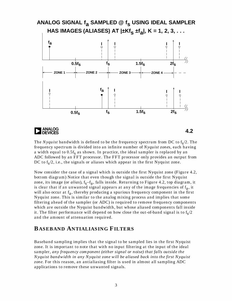
Properly specifying the antialiasing filter is important. The first step is to know thecharacteristics of the signal being sampled. Assume that the highest frequency ofinterest is fa. The antialiasing filter passes signals from DC to fa while attenuatingsignals above fa.
Assume that the corner frequency of the filter is chosen to be equal to fa. The effectof the finite transition from minimum to maximum attenuation on system dynamicrange is illustrated in Figure 4.3.
a
EFFECTS OF ANTIALIASING FILTERON SYSTEM DYNAMIC RANGE
4.3
fa
STOPBAND ATTENUATION = DR
TRANSITION BAND: fa TO fs - fa
CORNER FREQUENCY: fa
fs ffs - fafs
2
fs - fafa
DR
FILTERSPECIFICATIONS
Assume that the input signal has fullscale components well above the maximumfrequency of interest, fa. The diagram shows how fullscale frequency componentsabove fs – fa are aliased back into the bandwidth DC to fa. These aliasedcomponents are indistinguishable from actual signals and therefore limit thedynamic range to the value on the diagram which is shown as DR.
Some texts recommend specifying the antialiasing filter with respect to the Nyquistfrequency, fs/2, but this assumes that the signal bandwidth of interest extends fromDC to fs/2 which is rarely the case. In the example shown in Figure 4.3, the aliasedcomponents between fa and fs/2 are not of interest and do not limit the dynamicrange.
The antialiasing filter transition band is therefore determined by the cornerfrequency fa, the stopband frequency fs – fa, and the stopband attenuation, DR. Therequired system dynamic range is chosen based on our requirement for signalfidelity.
5
Filters have to become more complex as the transition band becomes sharper, allother things being equal. For instance, a Butterworth filter gives 6dB attenuationper octave for each filter pole. Achieving 60dB attenuation in a transition regionbetween 1MHz and 2MHz (1 octave) requires a minimum of 10 poles, not a trivialfilter, and definitely a design challenge.
Therefore, other filter types are generally more suited to high speed applicationswhere the requirement is for a sharp transition band and in-band flatness coupledwith linear phase response. Elliptic filters meet these criteria and are a popularchoice.
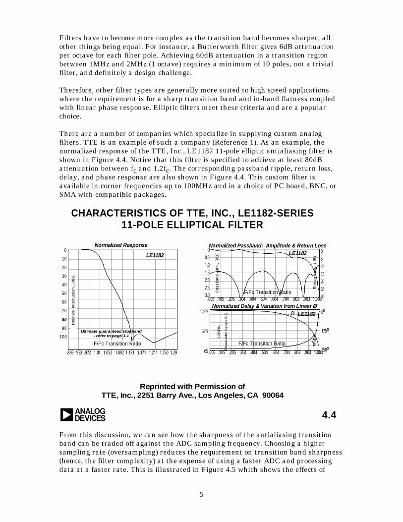
There are a number of companies which specialize in supplying custom analogfilters. TTE is an example of such a company (Reference 1). As an example, thenormalized response of the TTE, Inc., LE1182 11-pole elliptic antialiasing filter isshown in Figure 4.4. Notice that this filter is specified to achieve at least 80dBattenuation between fc and 1.2fc. The corresponding passband ripple, return loss,delay, and phase response are also shown in Figure 4.4. This custom filter isavailable in corner frequencies up to 100MHz and in a choice of PC board, BNC, orSMA with compatible packages.
a
CHARACTERISTICS OF TTE, INC., LE1182-SERIES11-POLE ELLIPTICAL FILTER
4.4
Reprinted with Permission ofTTE, Inc., 2251 Barry Ave., Los Angeles, CA 90064
0
10
20
30
40
50
60
70
80
90
100
.893 933 .972 1.01 1.052 1.092 1.131 1.171 1.211 1.250 1.29
LE1182
Normalized Response Normalized Passband: Amplitude & Return Loss
Normalized Delay & Variation from Linear O
Ultimate guaranteed stopband- refer to page 3-1
F/Fc Transition Ratio
LE1182
LE1182
.005 .105 .205 .304 .404 .504 .604 .704 .803 .903 1.003
0
5
10
15
20
25
30F/Fc Transition Ratio
F/Fc Transition Ratio
0
0.5
1.0
1.5
2.0
2.5
3.0
12.6S
6.6S
.6S
1.2S
/Div.
(Ple
ase
refe
r to p
age
3-3
)
.005 .105 .205 .304 .404 .504 .604 .704 .803 .903 1.003
0o
175o
350o
O
Rel
ativ
e A
tte
nua
tion
, (d
B)
Pas
sban
d A
ttn.
, (d
B)
Re
turn
Los
s, (
dB)
35o /D
iv.
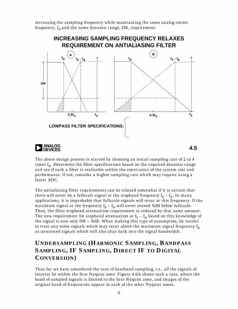
From this discussion, we can see how the sharpness of the antialiasing transitionband can be traded off against the ADC sampling frequency. Choosing a highersampling rate (oversampling) reduces the requirement on transition band sharpness(hence, the filter complexity) at the expense of using a faster ADC and processingdata at a faster rate. This is illustrated in Figure 4.5 which shows the effects of
6
increasing the sampling frequency while maintaining the same analog cornerfrequency, fa,and the same dynamic range, DR, requirement.
a 4.5
INCREASING SAMPLING FREQUENCY RELAXESREQUIREMENT ON ANTIALIASING FILTER
fs
BA
DR
0.5fs0.5fs fs
fa fs - fa fs - fafa
LOWPASS FILTER SPECIFICATIONS:
The above design process is started by choosing an initial sampling rate of 2 to 4times fa. Determine the filter specifications based on the required dynamic rangeand see if such a filter is realizable within the constraints of the system cost andperformance. If not, consider a higher sampling rate which may require using afaster ADC.
The antialiasing filter requirements can be relaxed somewhat if it is certain thatthere will never be a fullscale signal at the stopband frequency fs – fa. In manyapplications, it is improbable that fullscale signals will occur at this frequency. If themaximum signal at the frequency fs – fa will never exceed XdB below fullscale.Then, the filter stopband attenuation requirement is reduced by that same amount.The new requirement for stopband attenuation at fs – fa based on this knowledge ofthe signal is now only DR – XdB. When making this type of assumption, be carefulto treat any noise signals which may occur above the maximum signal frequency faas unwanted signals which will also alias back into the signal bandwidth.
UNDERSAMPLING (HARMONIC SAMPLING, BANDPASSSAMPLING, IF SAMPLING, DIRECT IF TO DIGITALCONVERSION)
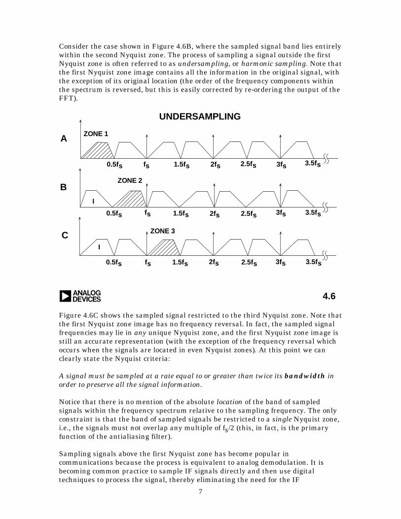
Thus far we have considered the case of baseband sampling, i.e., all the signals ofinterest lie within the first Nyquist zone. Figure 4.6A shows such a case, where theband of sampled signals is limited to the first Nyquist zone, and images of theoriginal band of frequencies appear in each of the other Nyquist zones.
7
Consider the case shown in Figure 4.6B, where the sampled signal band lies entirelywithin the second Nyquist zone. The process of sampling a signal outside the firstNyquist zone is often referred to as undersampling, or harmonic sampling. Note thatthe first Nyquist zone image contains all the information in the original signal, withthe exception of its original location (the order of the frequency components withinthe spectrum is reversed, but this is easily corrected by re-ordering the output of theFFT).
a
UNDERSAMPLING
4.6
A
B
C
ZONE 1
ZONE 2
ZONE 3
I
I
0.5fs
0.5fs
0.5fs
fs
fs
fs
1.5fs
1.5fs
1.5fs
2fs
2fs
2fs 2.5fs
2.5fs
2.5fs 3fs
3fs
3fs 3.5fs
3.5fs
3.5fs
Figure 4.6C shows the sampled signal restricted to the third Nyquist zone. Note thatthe first Nyquist zone image has no frequency reversal. In fact, the sampled signalfrequencies may lie in any unique Nyquist zone, and the first Nyquist zone image isstill an accurate representation (with the exception of the frequency reversal whichoccurs when the signals are located in even Nyquist zones). At this point we canclearly state the Nyquist criteria:
A signal must be sampled at a rate equal to or greater than twice its bandwidth inorder to preserve all the signal information.
Notice that there is no mention of the absolute location of the band of sampledsignals within the frequency spectrum relative to the sampling frequency. The onlyconstraint is that the band of sampled signals be restricted to a single Nyquist zone,i.e., the signals must not overlap any multiple of fs/2 (this, in fact, is the primaryfunction of the antialiasing filter).
Sampling signals above the first Nyquist zone has become popular incommunications because the process is equivalent to analog demodulation. It isbecoming common practice to sample IF signals directly and then use digitaltechniques to process the signal, thereby eliminating the need for the IF
8
demodulator. Clearly, however, as the IF frequencies become higher, the dynamicperformance requirements on the ADC become more critical. The ADC inputbandwidth and distortion performance must be adequate at the IF frequency, ratherthan only baseband. This presents a problem for most ADCs designed to processsignals in the first Nyquist zone, therefore an ADC suitable for undersamplingapplications must maintain dynamic performance into the higher order Nyquistzones.
ANTIALIASING FILTERS IN UNDERSAMPLINGAPPLICATIONS
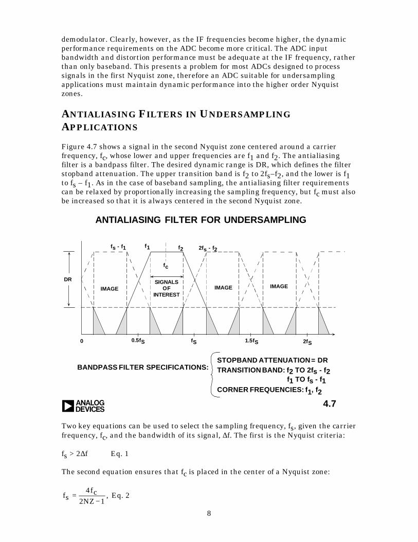
Figure 4.7 shows a signal in the second Nyquist zone centered around a carrierfrequency, fc, whose lower and upper frequencies are f1 and f2. The antialiasingfilter is a bandpass filter. The desired dynamic range is DR, which defines the filterstopband attenuation. The upper transition band is f2 to 2fs–f2, and the lower is f1to fs – f1. As in the case of baseband sampling, the antialiasing filter requirementscan be relaxed by proportionally increasing the sampling frequency, but fc must alsobe increased so that it is always centered in the second Nyquist zone.
a 4.7
ANTIALIASING FILTER FOR UNDERSAMPLING
DR
0.5fS fS
fs - f1
BANDPASS FILTER SPECIFICATIONS:STOPBAND ATTENUATION = DRTRANSITION BAND: f2 TO 2fs - f2
CORNER FREQUENCIES: f1, f2
f1 f2 2fs - f2
1.5fS 2fS0
IMAGESIGNALS
OFINTEREST
IMAGE IMAGE
fc
f1 TO fs - f1
Two key equations can be used to select the sampling frequency, fs, given the carrierfrequency, fc, and the bandwidth of its signal, ∆f. The first is the Nyquist criteria:
fs > 2∆f Eq. 1
The second equation ensures that fc is placed in the center of a Nyquist zone:
fsfc
NZ=
−4
2 1, Eq. 2
9
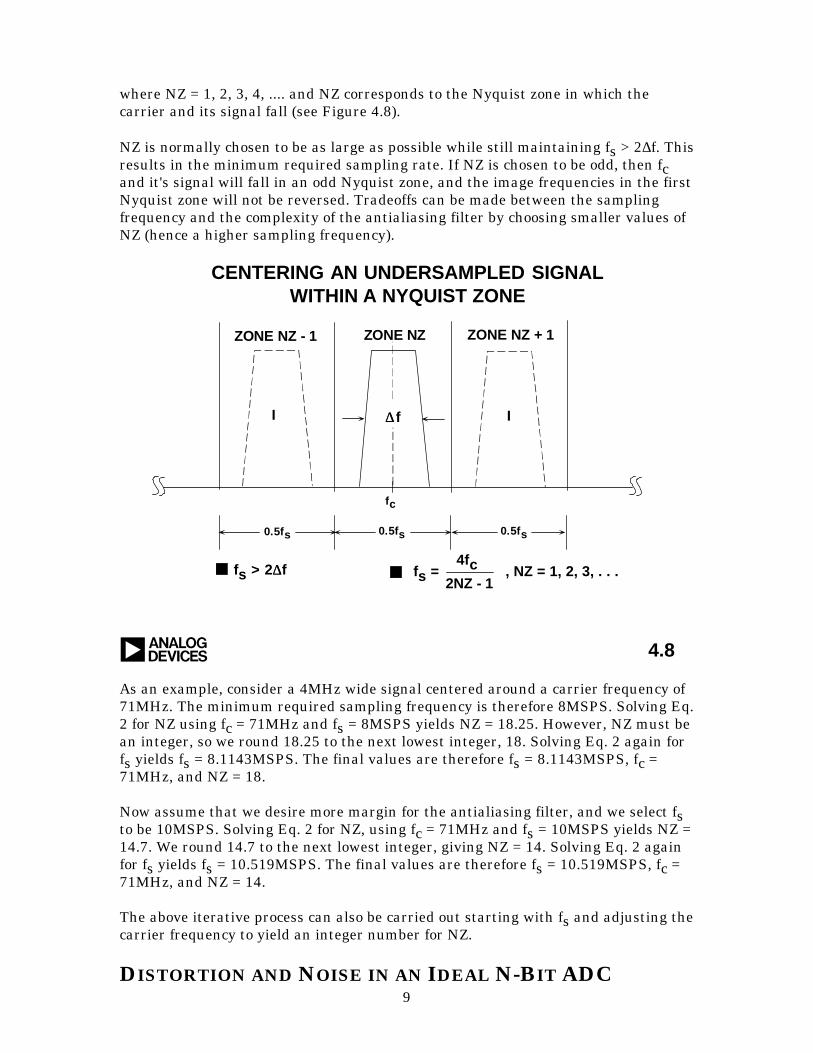
where NZ = 1, 2, 3, 4, .... and NZ corresponds to the Nyquist zone in which thecarrier and its signal fall (see Figure 4.8).
NZ is normally chosen to be as large as possible while still maintaining fs > 2∆f. Thisresults in the minimum required sampling rate. If NZ is chosen to be odd, then fcand it's signal will fall in an odd Nyquist zone, and the image frequencies in the firstNyquist zone will not be reversed. Tradeoffs can be made between the samplingfrequency and the complexity of the antialiasing filter by choosing smaller values ofNZ (hence a higher sampling frequency).
a 4.8
CENTERING AN UNDERSAMPLED SIGNALWITHIN A NYQUIST ZONE
0.5fs 0.5fs 0.5fs
II ∆∆ f
ZONE NZ - 1 ZONE NZ ZONE NZ + 1
fc
fs > 2∆∆f fs = , NZ = 1, 2, 3, . . .4fc
2NZ - 1
As an example, consider a 4MHz wide signal centered around a carrier frequency of71MHz. The minimum required sampling frequency is therefore 8MSPS. Solving Eq.2 for NZ using fc = 71MHz and fs = 8MSPS yields NZ = 18.25. However, NZ must bean integer, so we round 18.25 to the next lowest integer, 18. Solving Eq. 2 again forfs yields fs = 8.1143MSPS. The final values are therefore fs = 8.1143MSPS, fc =71MHz, and NZ = 18.
Now assume that we desire more margin for the antialiasing filter, and we select fsto be 10MSPS. Solving Eq. 2 for NZ, using fc = 71MHz and fs = 10MSPS yields NZ =14.7. We round 14.7 to the next lowest integer, giving NZ = 14. Solving Eq. 2 againfor fs yields fs = 10.519MSPS. The final values are therefore fs = 10.519MSPS, fc =71MHz, and NZ = 14.
The above iterative process can also be carried out starting with fs and adjusting thecarrier frequency to yield an integer number for NZ.
DISTORTION AND NOISE IN AN IDEAL N-BIT ADC
10
Thus far we have looked at the implications of the sampling process withoutconsidering the effects of ADC quantization. We will now treat the ADC as an idealsampler, but include the effects of quantization.
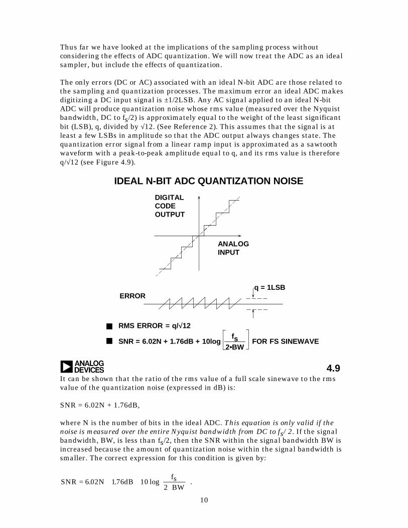
The only errors (DC or AC) associated with an ideal N-bit ADC are those related tothe sampling and quantization processes. The maximum error an ideal ADC makesdigitizing a DC input signal is ±1/2LSB. Any AC signal applied to an ideal N-bitADC will produce quantization noise whose rms value (measured over the Nyquistbandwidth, DC to fs/2) is approximately equal to the weight of the least significantbit (LSB), q, divided by √12. (See Reference 2). This assumes that the signal is atleast a few LSBs in amplitude so that the ADC output always changes state. Thequantization error signal from a linear ramp input is approximated as a sawtoothwaveform with a peak-to-peak amplitude equal to q, and its rms value is thereforeq/√12 (see Figure 4.9).
SNR = 6.02N + 1.76dB + 10log FOR FS SINEWAVEfs
2•BW
a 4.9
IDEAL N-BIT ADC QUANTIZATION NOISE
DIGITALCODEOUTPUT
RMS ERROR = q/√√12
ANALOGINPUT
ERRORq = 1LSB
It can be shown that the ratio of the rms value of a full scale sinewave to the rmsvalue of the quantization noise (expressed in dB) is:
SNR = 6.02N + 1.76dB,
where N is the number of bits in the ideal ADC. This equation is only valid if thenoise is measured over the entire Nyquist bandwidth from DC to fs/2. If the signalbandwidth, BW, is less than fs/2, then the SNR within the signal bandwidth BW isincreased because the amount of quantization noise within the signal bandwidth issmaller. The correct expression for this condition is given by:
SNR N dBfsBW
= + +⋅
6 02 176 102
. . log .
11
The above equation reflects the condition called oversampling, where the samplingfrequency is higher than twice the signal bandwidth. The correction term is oftencalled processing gain. Notice that for a given signal bandwidth, doubling thesampling frequency increases the SNR by 3dB.
Although the rms value of the noise is accurately approximated q/√12, its frequencydomain content may be highly correlated to the AC input signal. For instance, thereis greater correlation for low amplitude periodic signals than for large amplituderandom signals. Quite often, the assumption is made that the theoreticalquantization noise appears as white noise, spread uniformly over the Nyquistbandwidth DC to fs/2. Unfortunately, this is not true. In the case of strongcorrelation, the quantization noise appears concentrated at the various harmonics ofthe input signal, just where you don't want them.
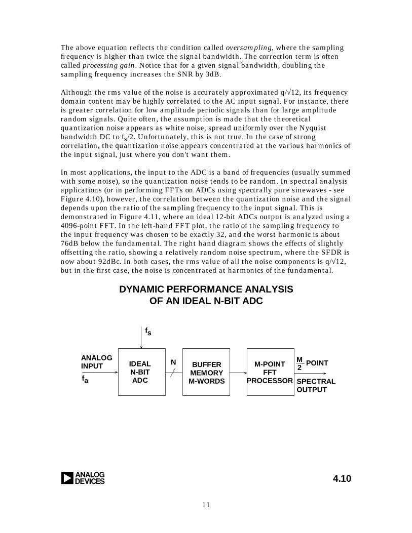
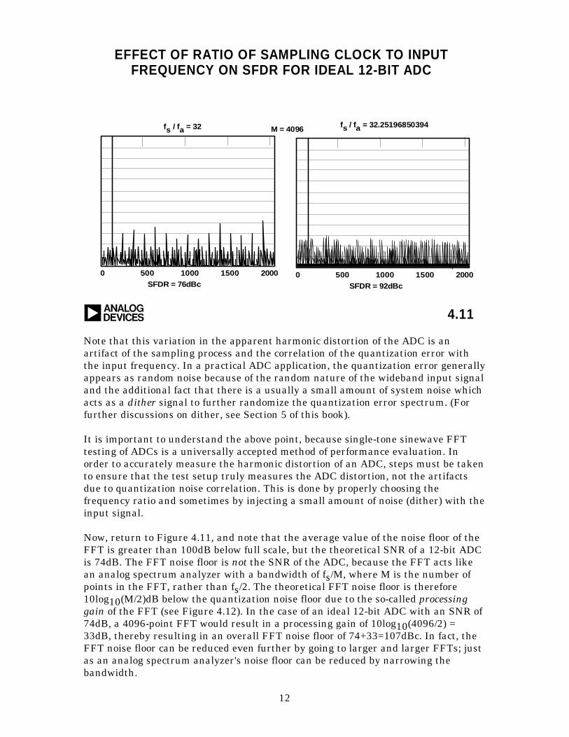
In most applications, the input to the ADC is a band of frequencies (usually summedwith some noise), so the quantization noise tends to be random. In spectral analysisapplications (or in performing FFTs on ADCs using spectrally pure sinewaves - seeFigure 4.10), however, the correlation between the quantization noise and the signaldepends upon the ratio of the sampling frequency to the input signal. This isdemonstrated in Figure 4.11, where an ideal 12-bit ADCs output is analyzed using a4096-point FFT. In the left-hand FFT plot, the ratio of the sampling frequency tothe input frequency was chosen to be exactly 32, and the worst harmonic is about76dB below the fundamental. The right hand diagram shows the effects of slightlyoffsetting the ratio, showing a relatively random noise spectrum, where the SFDR isnow about 92dBc. In both cases, the rms value of all the noise components is q/√12,but in the first case, the noise is concentrated at harmonics of the fundamental.
4.10
DYNAMIC PERFORMANCE ANALYSISOF AN IDEAL N-BIT ADC
a
ANALOGINPUT
fa
fs
N M2
POINT
SPECTRALOUTPUT
IDEALN-BITADC
BUFFERMEMORYM-WORDS
M-POINTFFT
PROCESSOR
12
4.11
EFFECT OF RATIO OF SAMPLING CLOCK TO INPUTFREQUENCY ON SFDR FOR IDEAL 12-BIT ADC
a
fs / fa = 32
0 500 1000 1500 2000 0 500 1000 1500 2000
M = 4096fs / fa = 32.25196850394
SFDR = 76dBc SFDR = 92dBc
Note that this variation in the apparent harmonic distortion of the ADC is anartifact of the sampling process and the correlation of the quantization error withthe input frequency. In a practical ADC application, the quantization error generallyappears as random noise because of the random nature of the wideband input signaland the additional fact that there is a usually a small amount of system noise whichacts as a dither signal to further randomize the quantization error spectrum. (Forfurther discussions on dither, see Section 5 of this book).
It is important to understand the above point, because single-tone sinewave FFTtesting of ADCs is a universally accepted method of performance evaluation. Inorder to accurately measure the harmonic distortion of an ADC, steps must be takento ensure that the test setup truly measures the ADC distortion, not the artifactsdue to quantization noise correlation. This is done by properly choosing thefrequency ratio and sometimes by injecting a small amount of noise (dither) with theinput signal.
Now, return to Figure 4.11, and note that the average value of the noise floor of theFFT is greater than 100dB below full scale, but the theoretical SNR of a 12-bit ADCis 74dB. The FFT noise floor is not the SNR of the ADC, because the FFT acts likean analog spectrum analyzer with a bandwidth of fs/M, where M is the number ofpoints in the FFT, rather than fs/2. The theoretical FFT noise floor is therefore10log10(M/2)dB below the quantization noise floor due to the so-called processinggain of the FFT (see Figure 4.12). In the case of an ideal 12-bit ADC with an SNR of74dB, a 4096-point FFT would result in a processing gain of 10log10(4096/2) =33dB, thereby resulting in an overall FFT noise floor of 74+33=107dBc. In fact, theFFT noise floor can be reduced even further by going to larger and larger FFTs; justas an analog spectrum analyzer's noise floor can be reduced by narrowing thebandwidth.
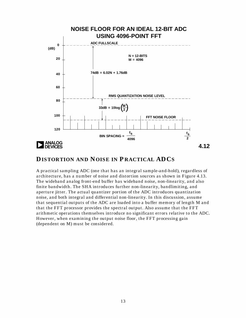
13
4.12
NOISE FLOOR FOR AN IDEAL 12-BIT ADCUSING 4096-POINT FFT
a
(dB)0
20
40
60
100 FFT NOISE FLOOR
fs
80
120
RMS QUANTIZATION NOISE LEVEL
2
fs
4096
33dB = 10log
BIN SPACING =
74dB = 6.02N + 1.76dB
ADC FULLSCALE
N = 12-BITSM = 4096
M2( )
DISTORTION AND NOISE IN PRACTICAL ADCS
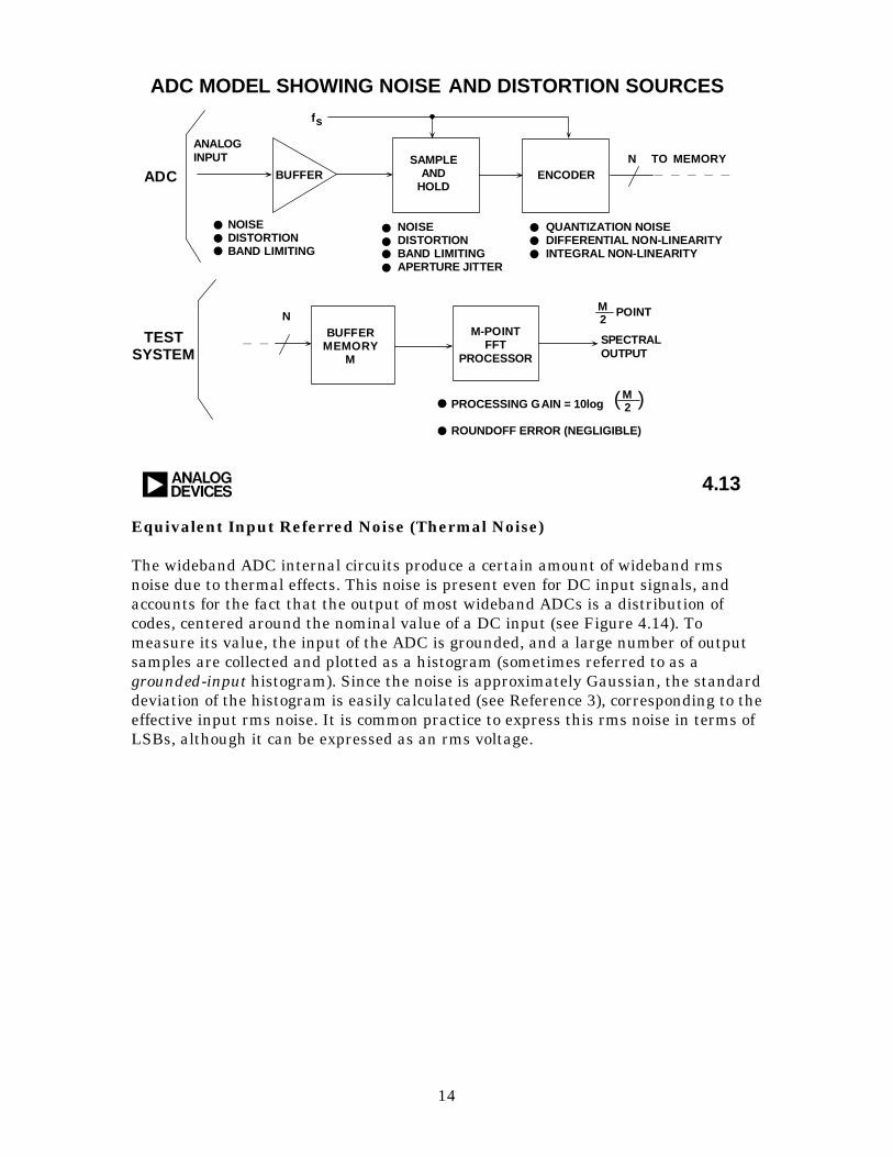
A practical sampling ADC (one that has an integral sample-and-hold), regardless ofarchitecture, has a number of noise and distortion sources as shown in Figure 4.13.The wideband analog front-end buffer has wideband noise, non-linearity, and alsofinite bandwidth. The SHA introduces further non-linearity, bandlimiting, andaperture jitter. The actual quantizer portion of the ADC introduces quantizationnoise, and both integral and differential non-linearity. In this discussion, assumethat sequential outputs of the ADC are loaded into a buffer memory of length M andthat the FFT processor provides the spectral output. Also assume that the FFTarithmetic operations themselves introduce no significant errors relative to the ADC.However, when examining the output noise floor, the FFT processing gain(dependent on M) must be considered.
14
M2PROCESSING GAIN = 10log
ROUNDOFF ERROR (NEGLIGIBLE)
( )
a 4.13
fs
ADC MODEL SHOWING NOISE AND DISTORTION SOURCES
ADC
N
N
TESTSYSTEM
ANALOGINPUT
NOISEDISTORTIONBAND LIMITING
•••NOISEDISTORTIONBAND LIMITINGAPERTURE JITTER
•••••••
QUANTIZATION NOISEDIFFERENTIAL NON-LINEARITYINTEGRAL NON-LINEARITY
TO MEMORY
••
BUFFERSAMPLE
ANDHOLD
ENCODER
M-POINTFFT
PROCESSOR
BUFFERMEMORY
M
M2 POINT
SPECTRALOUTPUT
Equivalent Input Referred Noise (Thermal Noise)
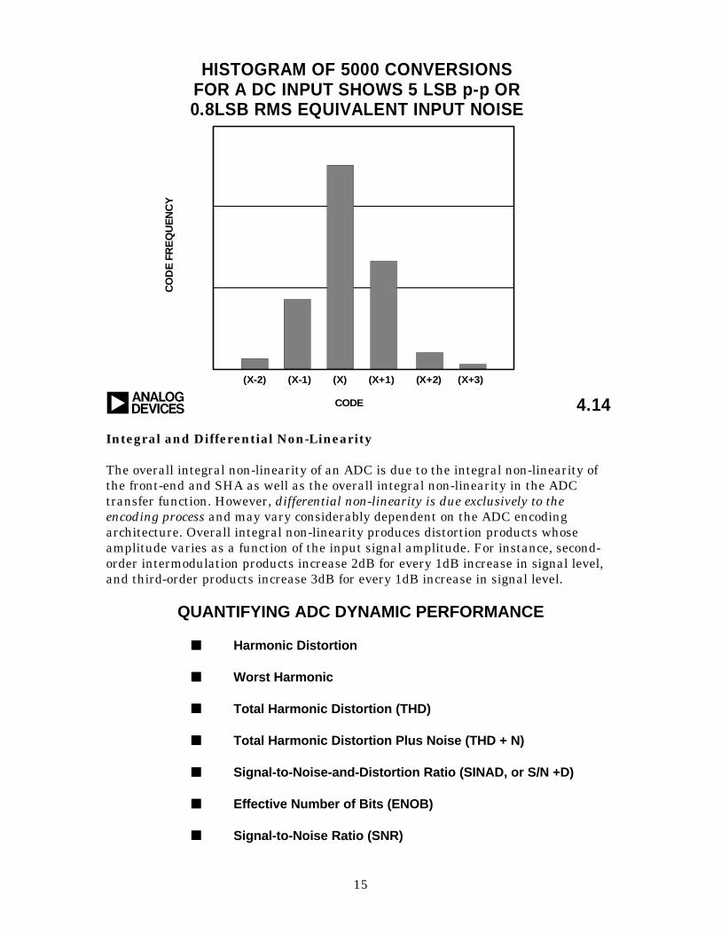
The wideband ADC internal circuits produce a certain amount of wideband rmsnoise due to thermal effects. This noise is present even for DC input signals, andaccounts for the fact that the output of most wideband ADCs is a distribution ofcodes, centered around the nominal value of a DC input (see Figure 4.14). Tomeasure its value, the input of the ADC is grounded, and a large number of outputsamples are collected and plotted as a histogram (sometimes referred to as agrounded-input histogram). Since the noise is approximately Gaussian, the standarddeviation of the histogram is easily calculated (see Reference 3), corresponding to theeffective input rms noise. It is common practice to express this rms noise in terms ofLSBs, although it can be expressed as an rms voltage.
15
4.14
HISTOGRAM OF 5000 CONVERSIONSFOR A DC INPUT SHOWS 5 LSB p-p OR0.8LSB RMS EQUIVALENT INPUT NOISE
a CODE
(X-2) (X-1) (X) (X+1) (X+2) (X+3)
CO
DE
FR
EQ
UE
NC
Y
Integral and Differential Non-Linearity
The overall integral non-linearity of an ADC is due to the integral non-linearity ofthe front-end and SHA as well as the overall integral non-linearity in the ADCtransfer function. However, differential non-linearity is due exclusively to theencoding process and may vary considerably dependent on the ADC encodingarchitecture. Overall integral non-linearity produces distortion products whoseamplitude varies as a function of the input signal amplitude. For instance, second-order intermodulation products increase 2dB for every 1dB increase in signal level,and third-order products increase 3dB for every 1dB increase in signal level.
QUANTIFYING ADC DYNAMIC PERFORMANCE
nn Harmonic Distortion
nn Worst Harmonic
nn Total Harmonic Distortion (THD)
nn Total Harmonic Distortion Plus Noise (THD + N)
nn Signal-to-Noise-and-Distortion Ratio (SINAD, or S/N +D)
nn Effective Number of Bits (ENOB)
nn Signal-to-Noise Ratio (SNR)
16
nn Analog Bandwidth (Full-Power, Small-Signal)
nn Spurious Free Dynamic Range (SFDR)
nn Two-Tone Intermodulation Distortion
nn Noise Power Ratio (NPR)
a 4.15
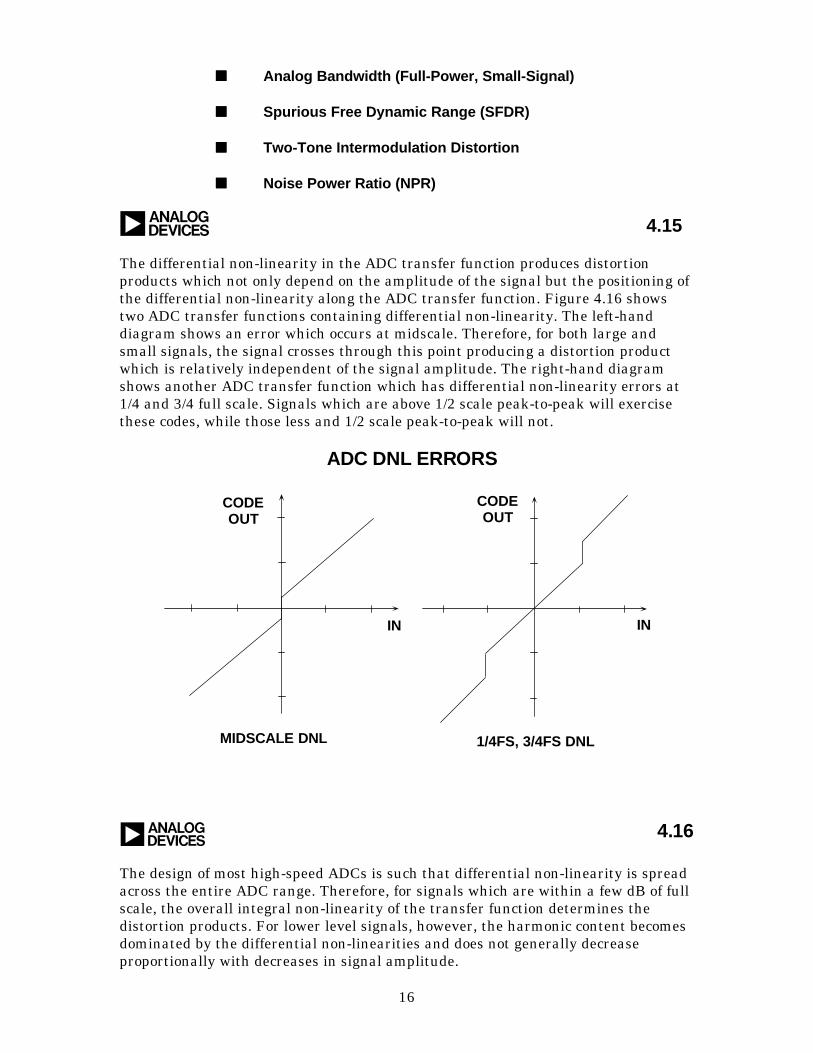
The differential non-linearity in the ADC transfer function produces distortionproducts which not only depend on the amplitude of the signal but the positioning ofthe differential non-linearity along the ADC transfer function. Figure 4.16 showstwo ADC transfer functions containing differential non-linearity. The left-handdiagram shows an error which occurs at midscale. Therefore, for both large andsmall signals, the signal crosses through this point producing a distortion productwhich is relatively independent of the signal amplitude. The right-hand diagramshows another ADC transfer function which has differential non-linearity errors at1/4 and 3/4 full scale. Signals which are above 1/2 scale peak-to-peak will exercisethese codes, while those less and 1/2 scale peak-to-peak will not.
4.16
ADC DNL ERRORS
a
CODEOUT
CODEOUT
IN IN
MIDSCALE DNL 1/4FS, 3/4FS DNL
The design of most high-speed ADCs is such that differential non-linearity is spreadacross the entire ADC range. Therefore, for signals which are within a few dB of fullscale, the overall integral non-linearity of the transfer function determines thedistortion products. For lower level signals, however, the harmonic content becomesdominated by the differential non-linearities and does not generally decreaseproportionally with decreases in signal amplitude.
17
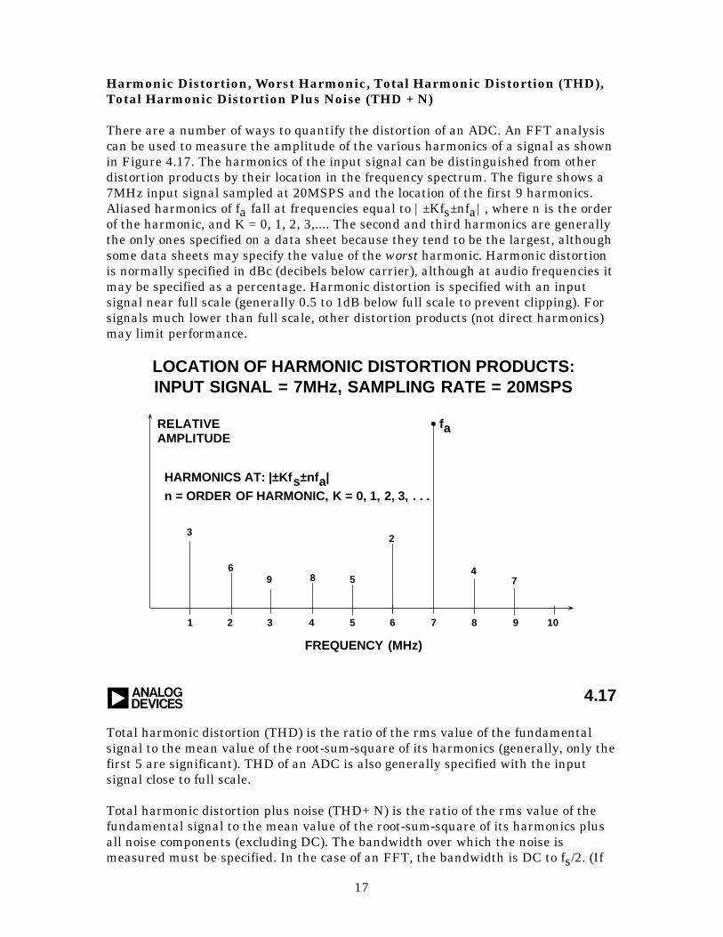
Harmonic Distortion, Worst Harmonic, Total Harmonic Distortion (THD),Total Harmonic Distortion Plus Noise (THD + N)
There are a number of ways to quantify the distortion of an ADC. An FFT analysiscan be used to measure the amplitude of the various harmonics of a signal as shownin Figure 4.17. The harmonics of the input signal can be distinguished from otherdistortion products by their location in the frequency spectrum. The figure shows a7MHz input signal sampled at 20MSPS and the location of the first 9 harmonics.Aliased harmonics of fa fall at frequencies equal to |±Kfs±nfa|, where n is the orderof the harmonic, and K = 0, 1, 2, 3,.... The second and third harmonics are generallythe only ones specified on a data sheet because they tend to be the largest, althoughsome data sheets may specify the value of the worst harmonic. Harmonic distortionis normally specified in dBc (decibels below carrier), although at audio frequencies itmay be specified as a percentage. Harmonic distortion is specified with an inputsignal near full scale (generally 0.5 to 1dB below full scale to prevent clipping). Forsignals much lower than full scale, other distortion products (not direct harmonics)may limit performance.
4.17
LOCATION OF HARMONIC DISTORTION PRODUCTS:INPUT SIGNAL = 7MHz, SAMPLING RATE = 20MSPS
a
RELATIVEAMPLITUDE
FREQUENCY (MHz)
fa
1 2 3 4 5 6 7 8 9 10
3
69 8 5 7
HARMONICS AT: |±Kfs±nfa|
n = ORDER OF HARMONIC, K = 0, 1, 2, 3, . . .
2
4
Total harmonic distortion (THD) is the ratio of the rms value of the fundamentalsignal to the mean value of the root-sum-square of its harmonics (generally, only thefirst 5 are significant). THD of an ADC is also generally specified with the inputsignal close to full scale.
Total harmonic distortion plus noise (THD+ N) is the ratio of the rms value of thefundamental signal to the mean value of the root-sum-square of its harmonics plusall noise components (excluding DC). The bandwidth over which the noise ismeasured must be specified. In the case of an FFT, the bandwidth is DC to fs/2. (If
18
the bandwidth of the measurement is DC to fs/2, THD+N is equal to SINAD - seebelow).
Signal-to-Noise-and-Distortion Ratio (SINAD), Signal-to-Noise Ratio (SNR),and Effective Number of Bits (ENOB)
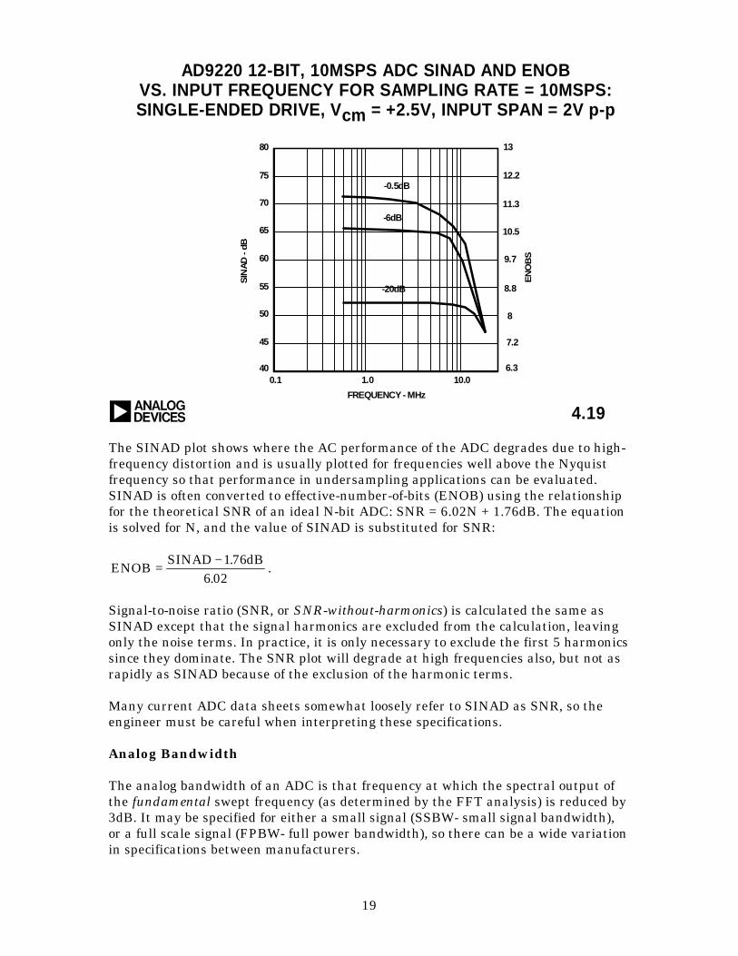
SINAD and SNR deserve careful attention, because there is still some variationbetween ADC manufacturers as to their precise meaning. Signal-to-noise-andDistortion (SINAD, or S/N+D) is the ratio of the rms signal amplitude to the meanvalue of the root-sum-square (RSS) of all other spectral components, includingharmonics, but excluding DC. SINAD is a good indication of the overall dynamicperformance of an ADC as a function of input frequency because it includes allcomponents which make up noise (including thermal noise) and distortion. It is oftenplotted for various input amplitudes. SINAD is equal to THD+N if the bandwidth forthe noise measurement is the same. A typical plot for the AD9220 12-bit, 10MSPSADC is shown in Figure 4.19.
SINAD, ENOB, AND SNR
nn SINAD (Signal-to-Noise-and-Distortion Ratio):
The ratio of the rms signal amplitude to the mean value ofthe root-sum-squares (RSS) of all other spectral components,including harmonics, but excluding DC
nn ENOB (Effective Number of Bits):
ENOBSINAD dB
==−− 176
6 02.
.
nn SNR (Signal-to-Noise Ratio, or Signal-to-Noise RatioWithout Harmonics):
The ratio of the rms signal amplitude to the mean value ofthe root-sum-squares (RSS) of all other spectral components,excluding the first 5 harmonics and DC
a 4.18
19
4.19
AD9220 12-BIT, 10MSPS ADC SINAD AND ENOBVS. INPUT FREQUENCY FOR SAMPLING RATE = 10MSPS:SINGLE-ENDED DRIVE, Vcm = +2.5V, INPUT SPAN = 2V p-p
a
65
FREQUENCY MHz
80
75
40
70
45
60
55
50
0.1 1.0 10.0
0.5dB
6dB
20dB
13
SIN
AD
- dB
12.2
11.3
10.5
9.7
8.8
8
7.2
6.3
EN
OB
S
The SINAD plot shows where the AC performance of the ADC degrades due to high-frequency distortion and is usually plotted for frequencies well above the Nyquistfrequency so that performance in undersampling applications can be evaluated.SINAD is often converted to effective-number-of-bits (ENOB) using the relationshipfor the theoretical SNR of an ideal N-bit ADC: SNR = 6.02N + 1.76dB. The equationis solved for N, and the value of SINAD is substituted for SNR:
ENOBSINAD dB
=−176
6 02.
..
Signal-to-noise ratio (SNR, or SNR-without-harmonics) is calculated the same asSINAD except that the signal harmonics are excluded from the calculation, leavingonly the noise terms. In practice, it is only necessary to exclude the first 5 harmonicssince they dominate. The SNR plot will degrade at high frequencies also, but not asrapidly as SINAD because of the exclusion of the harmonic terms.
Many current ADC data sheets somewhat loosely refer to SINAD as SNR, so theengineer must be careful when interpreting these specifications.
Analog Bandwidth
The analog bandwidth of an ADC is that frequency at which the spectral output ofthe fundamental swept frequency (as determined by the FFT analysis) is reduced by3dB. It may be specified for either a small signal (SSBW- small signal bandwidth),or a full scale signal (FPBW- full power bandwidth), so there can be a wide variationin specifications between manufacturers.
20
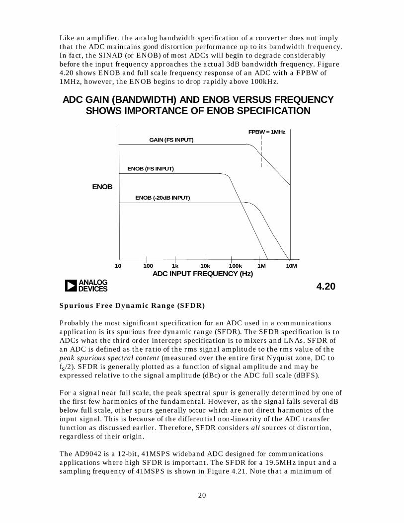
Like an amplifier, the analog bandwidth specification of a converter does not implythat the ADC maintains good distortion performance up to its bandwidth frequency.In fact, the SINAD (or ENOB) of most ADCs will begin to degrade considerablybefore the input frequency approaches the actual 3dB bandwidth frequency. Figure4.20 shows ENOB and full scale frequency response of an ADC with a FPBW of1MHz, however, the ENOB begins to drop rapidly above 100kHz.
a 4.20
ADC GAIN (BANDWIDTH) AND ENOB VERSUS FREQUENCYSHOWS IMPORTANCE OF ENOB SPECIFICATION
ADC INPUT FREQUENCY (Hz)
ENOB
GAIN (FS INPUT)
ENOB (FS INPUT)
ENOB (-20dB INPUT)
FPBW = 1MHz
10 100 1k 10k 100k 1M 10M
Spurious Free Dynamic Range (SFDR)
Probably the most significant specification for an ADC used in a communicationsapplication is its spurious free dynamic range (SFDR). The SFDR specification is toADCs what the third order intercept specification is to mixers and LNAs. SFDR ofan ADC is defined as the ratio of the rms signal amplitude to the rms value of thepeak spurious spectral content (measured over the entire first Nyquist zone, DC tofs/2). SFDR is generally plotted as a function of signal amplitude and may beexpressed relative to the signal amplitude (dBc) or the ADC full scale (dBFS).
For a signal near full scale, the peak spectral spur is generally determined by one ofthe first few harmonics of the fundamental. However, as the signal falls several dBbelow full scale, other spurs generally occur which are not direct harmonics of theinput signal. This is because of the differential non-linearity of the ADC transferfunction as discussed earlier. Therefore, SFDR considers all sources of distortion,regardless of their origin.
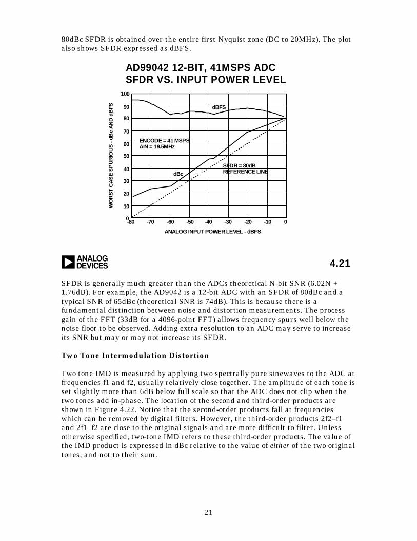
The AD9042 is a 12-bit, 41MSPS wideband ADC designed for communicationsapplications where high SFDR is important. The SFDR for a 19.5MHz input and asampling frequency of 41MSPS is shown in Figure 4.21. Note that a minimum of
21
80dBc SFDR is obtained over the entire first Nyquist zone (DC to 20MHz). The plotalso shows SFDR expressed as dBFS.
4.21
AD99042 12-BIT, 41MSPS ADCSFDR VS. INPUT POWER LEVEL
a
ANALOG INPUT POWER LEVEL dBFS
100
080 070 60 50 40 30 20 10
90
60
40
20
10
80
70
50
30
ENCODE = 41 MSPS AIN = 19.5MHz
dBFS
dBc
SFDR = 80dB REFERENCE LINE
WO
RS
T C
AS
E S
PU
RIO
US
- dB
c A
ND
dB
FS
SFDR is generally much greater than the ADCs theoretical N-bit SNR (6.02N +1.76dB). For example, the AD9042 is a 12-bit ADC with an SFDR of 80dBc and atypical SNR of 65dBc (theoretical SNR is 74dB). This is because there is afundamental distinction between noise and distortion measurements. The processgain of the FFT (33dB for a 4096-point FFT) allows frequency spurs well below thenoise floor to be observed. Adding extra resolution to an ADC may serve to increaseits SNR but may or may not increase its SFDR.
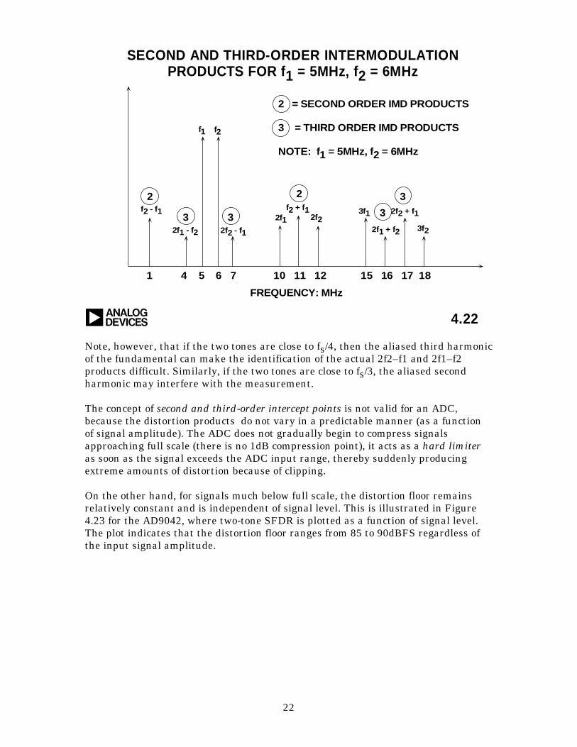
Two Tone Intermodulation Distortion
Two tone IMD is measured by applying two spectrally pure sinewaves to the ADC atfrequencies f1 and f2, usually relatively close together. The amplitude of each tone isset slightly more than 6dB below full scale so that the ADC does not clip when thetwo tones add in-phase. The location of the second and third-order products areshown in Figure 4.22. Notice that the second-order products fall at frequencieswhich can be removed by digital filters. However, the third-order products 2f2–f1and 2f1–f2 are close to the original signals and are more difficult to filter. Unlessotherwise specified, two-tone IMD refers to these third-order products. The value ofthe IMD product is expressed in dBc relative to the value of either of the two originaltones, and not to their sum.
22
a 4.22
SECOND AND THIRD-ORDER INTERMODULATIONPRODUCTS FOR f1 = 5MHz, f2 = 6MHz
FREQUENCY: MHz
2 = SECOND ORDER IMD PRODUCTS
3 = THIRD ORDER IMD PRODUCTS
NOTE: f1 = 5MHz, f2 = 6MHz
f2 - f1
2f1 - f2 2f2 - f1
f1 f2
2f1 2f2
f2 + f1
2f1 + f2
3f1 2f2 + f1
3f2
2
3 3
2
3
3
1 4 5 6 7 10 11 12 15 16 17 18
Note, however, that if the two tones are close to fs/4, then the aliased third harmonicof the fundamental can make the identification of the actual 2f2–f1 and 2f1–f2products difficult. Similarly, if the two tones are close to fs/3, the aliased secondharmonic may interfere with the measurement.
The concept of second and third-order intercept points is not valid for an ADC,because the distortion products do not vary in a predictable manner (as a functionof signal amplitude). The ADC does not gradually begin to compress signalsapproaching full scale (there is no 1dB compression point), it acts as a hard limiteras soon as the signal exceeds the ADC input range, thereby suddenly producingextreme amounts of distortion because of clipping.
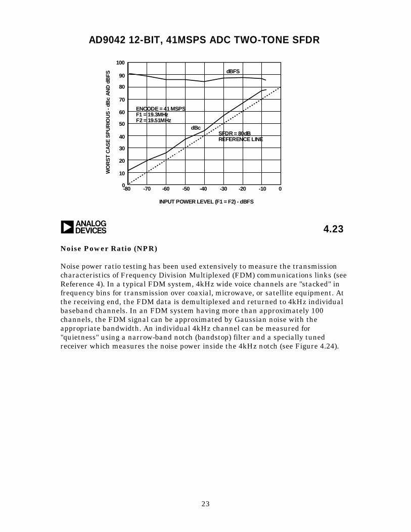
On the other hand, for signals much below full scale, the distortion floor remainsrelatively constant and is independent of signal level. This is illustrated in Figure4.23 for the AD9042, where two-tone SFDR is plotted as a function of signal level.The plot indicates that the distortion floor ranges from 85 to 90dBFS regardless ofthe input signal amplitude.
23
4.23
AD9042 12-BIT, 41MSPS ADC TWO-TONE SFDR
a
INPUT POWER LEVEL (F1 = F2) dBFS
100
080 070 60 50 40 30 20 10
90
60
40
20
10
80
70
50
30
ENCODE = 41 MSPS F1 = 19.3MHz F2 = 19.51MHz
SFDR = 80dB REFERENCE LINE
dBFS
dBc
WO
RS
T C
AS
E S
PU
RIO
US
- dB
c A
ND
dB
FS
Noise Power Ratio (NPR)
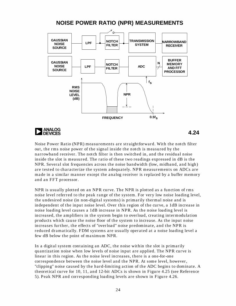
Noise power ratio testing has been used extensively to measure the transmissioncharacteristics of Frequency Division Multiplexed (FDM) communications links (seeReference 4). In a typical FDM system, 4kHz wide voice channels are "stacked" infrequency bins for transmission over coaxial, microwave, or satellite equipment. Atthe receiving end, the FDM data is demultiplexed and returned to 4kHz individualbaseband channels. In an FDM system having more than approximately 100channels, the FDM signal can be approximated by Gaussian noise with theappropriate bandwidth. An individual 4kHz channel can be measured for"quietness" using a narrow-band notch (bandstop) filter and a specially tunedreceiver which measures the noise power inside the 4kHz notch (see Figure 4.24).
24
a 4.24
NOISE POWER RATIO (NPR) MEASUREMENTS
fs
GAUSSIANNOISE
SOURCE
GAUSSIANNOISE
SOURCELPF
LPF NOTCHFILTER
NOTCHFILTER
NADC
TRANSMISSIONSYSTEM
NARROWBANDRECEIVER
BUFFERMEMORYAND FFT
PROCESSOR
0.5fs
RMSNOISELEVEL
(dB)NPR
FREQUENCY
Noise Power Ratio (NPR) measurements are straightforward. With the notch filterout, the rms noise power of the signal inside the notch is measured by thenarrowband receiver. The notch filter is then switched in, and the residual noiseinside the slot is measured. The ratio of these two readings expressed in dB is theNPR. Several slot frequencies across the noise bandwidth (low, midband, and high)are tested to characterize the system adequately. NPR measurements on ADCs aremade in a similar manner except the analog receiver is replaced by a buffer memoryand an FFT processor.
NPR is usually plotted on an NPR curve. The NPR is plotted as a function of rmsnoise level referred to the peak range of the system. For very low noise loading level,the undesired noise (in non-digital systems) is primarily thermal noise and isindependent of the input noise level. Over this region of the curve, a 1dB increase innoise loading level causes a 1dB increase in NPR. As the noise loading level isincreased, the amplifiers in the system begin to overload, creating intermodulationproducts which cause the noise floor of the system to increase. As the input noiseincreases further, the effects of "overload" noise predominate, and the NPR isreduced dramatically. FDM systems are usually operated at a noise loading level afew dB below the point of maximum NPR.
In a digital system containing an ADC, the noise within the slot is primarilyquantization noise when low levels of noise input are applied. The NPR curve islinear in this region. As the noise level increases, there is a one-for-onecorrespondence between the noise level and the NPR. At some level, however,"clipping" noise caused by the hard-limiting action of the ADC begins to dominate. Atheoretical curve for 10, 11, and 12-bit ADCs is shown in Figure 4.25 (see Reference5). Peak NPR and corresponding loading levels are shown in Figure 4.26.
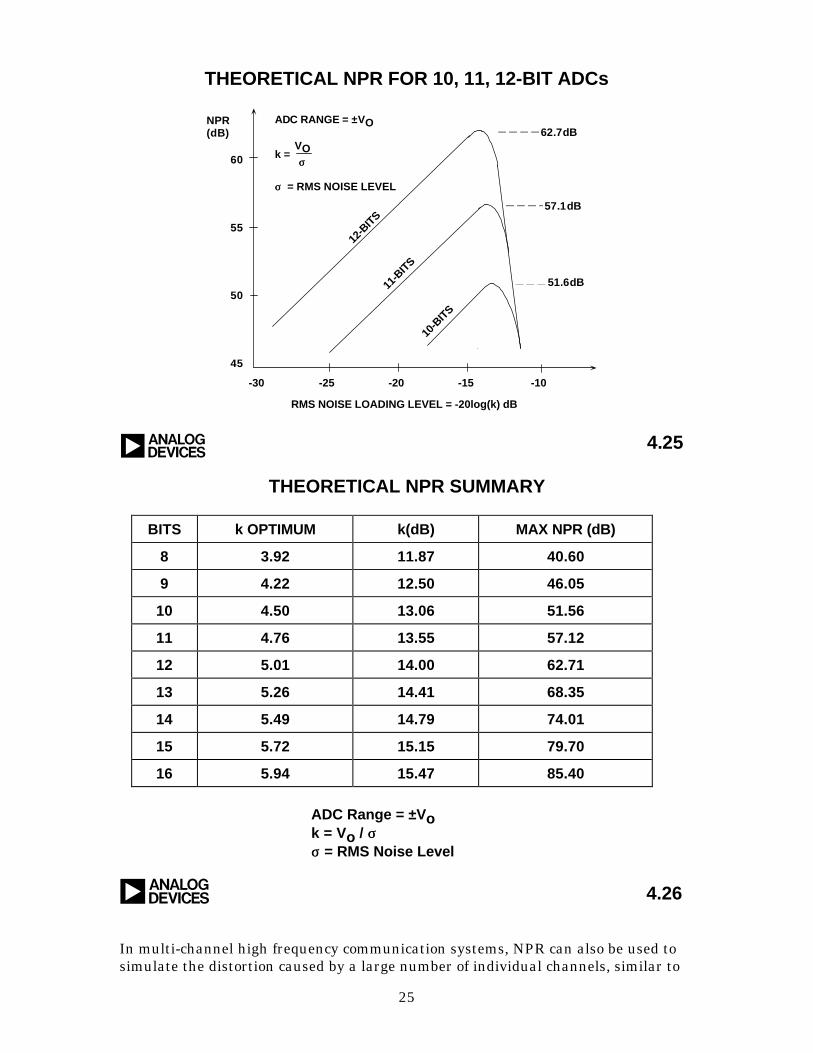
25
a 4.25
THEORETICAL NPR FOR 10, 11, 12-BIT ADCs
VOσσ
NPR(dB) 62.7dB
RMS NOISE LOADING LEVEL = -20log(k) dB
57.1dB
51.6dB
60
55
50
45
-30 -25 -20 -15 -10
ADC RANGE = ±VO
k =
σσ = RMS NOISE LEVEL
12-B
ITS
11-B
ITS
10-B
ITS
THEORETICAL NPR SUMMARY
BITS k OPTIMUM k(dB) MAX NPR (dB)
8 3.92 11.87 40.60
9 4.22 12.50 46.05
10 4.50 13.06 51.56
11 4.76 13.55 57.12
12 5.01 14.00 62.71
13 5.26 14.41 68.35
14 5.49 14.79 74.01
15 5.72 15.15 79.70
16 5.94 15.47 85.40
ADC Range = ±Vok = Vo / σσσσ = RMS Noise Level
a 4.26
In multi-channel high frequency communication systems, NPR can also be used tosimulate the distortion caused by a large number of individual channels, similar to
26
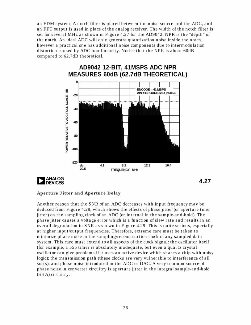
an FDM system. A notch filter is placed between the noise source and the ADC, andan FFT output is used in place of the analog receiver. The width of the notch filter isset for several MHz as shown in Figure 4.27 for the AD9042. NPR is the "depth" ofthe notch. An ideal ADC will only generate quantization noise inside the notch,however a practical one has additional noise components due to intermodulationdistortion caused by ADC non-linearity. Notice that the NPR is about 60dBcompared to 62.7dB theoretical.
4.27
AD9042 12-BIT, 41MSPS ADC NPRMEASURES 60dB (62.7dB THEORETICAL)
a
FREQUENCY - MHz
PO
WE
R R
ELA
TIV
E T
O A
DC
FU
LL
SC
AL
E -
dB
0
80
120
40
100
20
60
dc 4.1 8.2 12.3 16.420.5
ENCODE = 41 MSPS AIN = BROADBAND_NOISE
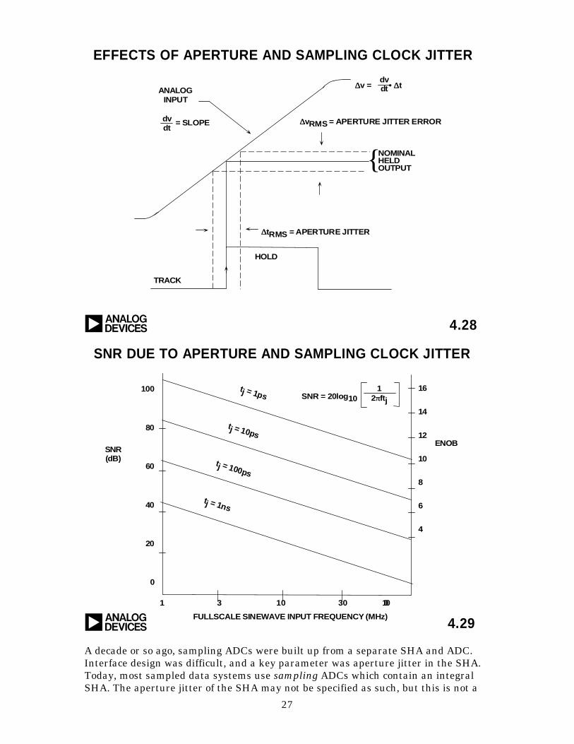
Aperture Jitter and Aperture Delay
Another reason that the SNR of an ADC decreases with input frequency may bededuced from Figure 4.28, which shows the effects of phase jitter (or aperture timejitter) on the sampling clock of an ADC (or internal in the sample-and-hold). Thephase jitter causes a voltage error which is a function of slew rate and results in anoverall degradation in SNR as shown in Figure 4.29. This is quite serious, especiallyat higher input/output frequencies. Therefore, extreme care must be taken tominimize phase noise in the sampling/reconstruction clock of any sampled datasystem. This care must extend to all aspects of the clock signal: the oscillator itself(for example, a 555 timer is absolutely inadequate, but even a quartz crystaloscillator can give problems if it uses an active device which shares a chip with noisylogic); the transmission path (these clocks are very vulnerable to interference of allsorts), and phase noise introduced in the ADC or DAC. A very common source ofphase noise in converter circuitry is aperture jitter in the integral sample-and-hold(SHA) circuitry.
27
a 4.28
EFFECTS OF APERTURE AND SAMPLING CLOCK JITTER
TRACK
NOMINALHELDOUTPUT
ANALOGINPUT
= SLOPEdvdt
HOLD
∆∆tRMS = APERTURE JITTER
∆∆vRMS = APERTURE JITTER ERROR
∆∆v = • ∆∆tdvdt
a 4.29
SNR DUE TO APERTURE AND SAMPLING CLOCK JITTER
SNR(dB)
ENOB
FULLSCALE SINEWAVE INPUT FREQUENCY (MHz)
100
80
60
40
20
0
16
14
12
10
8
6
4
1 3 10 30 100
SNR = 20log101
2ππftj
tj = 1ps
tj = 10ps
tj = 100ps
tj = 1ns
A decade or so ago, sampling ADCs were built up from a separate SHA and ADC.Interface design was difficult, and a key parameter was aperture jitter in the SHA.Today, most sampled data systems use sampling ADCs which contain an integralSHA. The aperture jitter of the SHA may not be specified as such, but this is not a
28
cause of concern if the SNR or ENOB is clearly specified, since a guarantee of aspecific SNR is an implicit guarantee of an adequate aperture jitter specification.However, the use of an additional high-performance SHA will sometimes improvethe high-frequency ENOB of a even the best sampling ADC by presenting "DC" tothe ADC, and may be more cost-effective than replacing the ADC with a moreexpensive one.
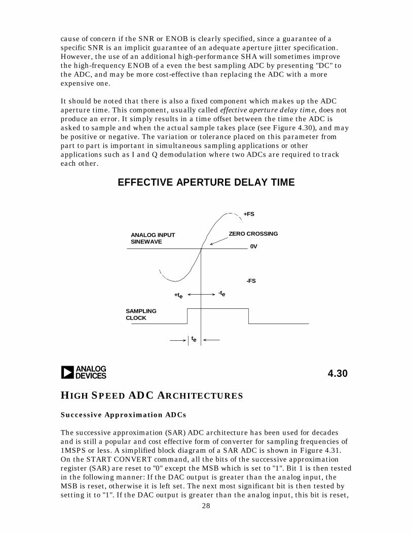
It should be noted that there is also a fixed component which makes up the ADCaperture time. This component, usually called effective aperture delay time, does notproduce an error. It simply results in a time offset between the time the ADC isasked to sample and when the actual sample takes place (see Figure 4.30), and maybe positive or negative. The variation or tolerance placed on this parameter frompart to part is important in simultaneous sampling applications or otherapplications such as I and Q demodulation where two ADCs are required to trackeach other.
a 4.30
EFFECTIVE APERTURE DELAY TIME
SAMPLINGCLOCK
ANALOG INPUTSINEWAVE
ZERO CROSSING
+FS
-FS
0V
+te-te
te
HIGH SPEED ADC ARCHITECTURES
Successive Approximation ADCs
The successive approximation (SAR) ADC architecture has been used for decadesand is still a popular and cost effective form of converter for sampling frequencies of1MSPS or less. A simplified block diagram of a SAR ADC is shown in Figure 4.31.On the START CONVERT command, all the bits of the successive approximationregister (SAR) are reset to "0" except the MSB which is set to "1". Bit 1 is then testedin the following manner: If the DAC output is greater than the analog input, theMSB is reset, otherwise it is left set. The next most significant bit is then tested bysetting it to "1". If the DAC output is greater than the analog input, this bit is reset,
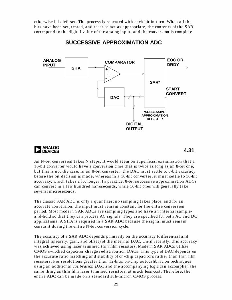
29
otherwise it is left set. The process is repeated with each bit in turn. When all thebits have been set, tested, and reset or not as appropriate, the contents of the SARcorrespond to the digital value of the analog input, and the conversion is complete.
4.31
SUCCESSIVE APPROXIMATION ADC
a
ANALOGINPUT
STARTCONVERT
COMPARATOR EOC ORDRDY
SHA +
-
DAC
SAR*
*SUCCESSIVE APPROXIMATION
REGISTER
DIGITALOUTPUT
An N-bit conversion takes N steps. It would seem on superficial examination that a16-bit converter would have a conversion time that is twice as long as an 8-bit one,but this is not the case. In an 8-bit converter, the DAC must settle to 8-bit accuracybefore the bit decision is made, whereas in a 16-bit converter, it must settle to 16-bitaccuracy, which takes a lot longer. In practice, 8-bit successive approximation ADCscan convert in a few hundred nanoseconds, while 16-bit ones will generally takeseveral microseconds.
The classic SAR ADC is only a quantizer: no sampling takes place, and for anaccurate conversion, the input must remain constant for the entire conversionperiod. Most modern SAR ADCs are sampling types and have an internal sample-and-hold so that they can process AC signals. They are specified for both AC and DCapplications. A SHA is required in a SAR ADC because the signal must remainconstant during the entire N-bit conversion cycle.
The accuracy of a SAR ADC depends primarily on the accuracy (differential andintegral linearity, gain, and offset) of the internal DAC. Until recently, this accuracywas achieved using laser trimmed thin film resistors. Modern SAR ADCs utilizeCMOS switched capacitor charge redistribution DACs. This type of DAC depends onthe accurate ratio matching and stability of on-chip capacitors rather than thin filmresistors. For resolutions greater than 12-bits, on-chip autocalibration techniquesusing an additional calibration DAC and the accompanying logic can accomplish thesame thing as thin film laser trimmed resistors, at much less cost. Therefore, theentire ADC can be made on a standard sub-micron CMOS process.
30
The successive approximation ADC has a very simple structure, is low power, andhas reasonably fast conversion times (<1MSPS). It is probably the most widely usedADC architecture, and will continue to be used for medium speed and mediumresolution applications.
Current 12-bit SAR ADCs achieve sampling rates up to about 1MSPS, and 16-bitones up to about 300kSPS. Examples of typical state-of-the-art SAR ADCs are theAD7892 (12-bits at 600kSPS), the AD976/977 (16-bits at 100kSPS), and the AD7882(16-bits at 300kSPS).
Flash Converters
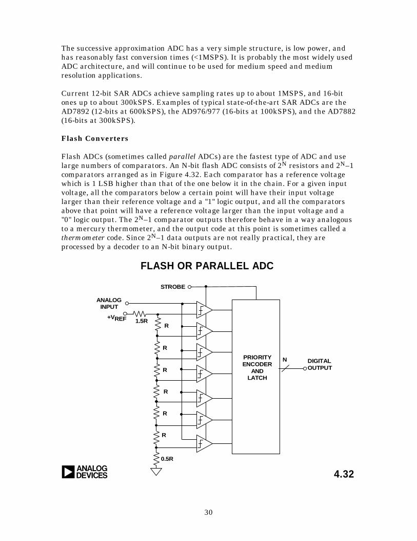
Flash ADCs (sometimes called parallel ADCs) are the fastest type of ADC and uselarge numbers of comparators. An N-bit flash ADC consists of 2N resistors and 2N–1comparators arranged as in Figure 4.32. Each comparator has a reference voltagewhich is 1 LSB higher than that of the one below it in the chain. For a given inputvoltage, all the comparators below a certain point will have their input voltagelarger than their reference voltage and a "1" logic output, and all the comparatorsabove that point will have a reference voltage larger than the input voltage and a"0" logic output. The 2N–1 comparator outputs therefore behave in a way analogousto a mercury thermometer, and the output code at this point is sometimes called athermometer code. Since 2N–1 data outputs are not really practical, they areprocessed by a decoder to an N-bit binary output.
a 4.32
FLASH OR PARALLEL ADC
ANALOGINPUT
DIGITALOUTPUT
N
R
R
R
R
R
R
0.5R
1.5R+VREF
STROBE
PRIORITYENCODER
ANDLATCH
31
The input signal is applied to all the comparators at once, so the thermometeroutput is delayed by only one comparator delay from the input, and the encoderN-bit output by only a few gate delays on top of that, so the process is very fast.However, the architecture uses large numbers of resistors and comparators and itlimited to low resolutions, and if it is to be fast, each comparator must run atrelatively high power levels. Hence, the problems of flash ADCs include limitedresolution, high power dissipation because of the large number of high speedcomparators (especially at sampling rates greater than 50MSPS), and relativelylarge (and therefore expensive) chip sizes. In addition, the resistance of the referenceresistor chain must be kept low to supply adequate bias current to the fastcomparators, so the voltage reference has to source quite large currents (>10 mA).
In practice, flash converters are available up to 10-bits, but more commonly theyhave 8-bits of resolution. Their maximum sampling rate can be as high as500 MSPS, and input full-power bandwidths in excess of 300 MHz.
But as mentioned earlier, full-power bandwidths are not necessarily full-resolutionbandwidths. Ideally, the comparators in a flash converter are well matched both forDC and AC characteristics. Because the strobe is applied to all the comparatorssimultaneously, the flash converter is inherently a sampling converter. In practice,there are delay variations between the comparators and other AC mismatches whichcause a degradation in ENOB at high input frequencies. This is because the inputsare slewing at a rate comparable to the comparator conversion time.
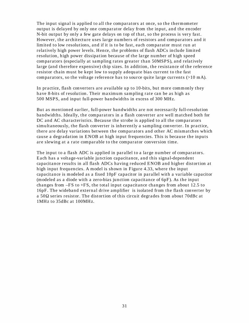
The input to a flash ADC is applied in parallel to a large number of comparators.Each has a voltage-variable junction capacitance, and this signal-dependentcapacitance results in all flash ADCs having reduced ENOB and higher distortion athigh input frequencies. A model is shown in Figure 4.33, where the inputcapacitance is modeled as a fixed 10pF capacitor in parallel with a variable capacitor(modeled as a diode with a zero-bias junction capacitance of 6pF). As the inputchanges from –FS to +FS, the total input capacitance changes from about 12.5 to16pF. The wideband external drive amplifier is isolated from the flash converter bya 50Ω series resistor. The distortion of this circuit degrades from about 70dBc at1MHz to 35dBc at 100MHz.
32
a 4.33
SIGNAL-DEPENDENT INPUT CAPACITANCE CAUSESDISTORTION AT HIGH FREQUENCIES
THD(dB)
70
60
50
40
301 10 100
ANALOGINPUT 50ΩΩ
-FS TO +FS
10pF
+FS
CJO = 6pF
FLASH INPUT MODEL
A
INPUT FREQUENCY (MHz)
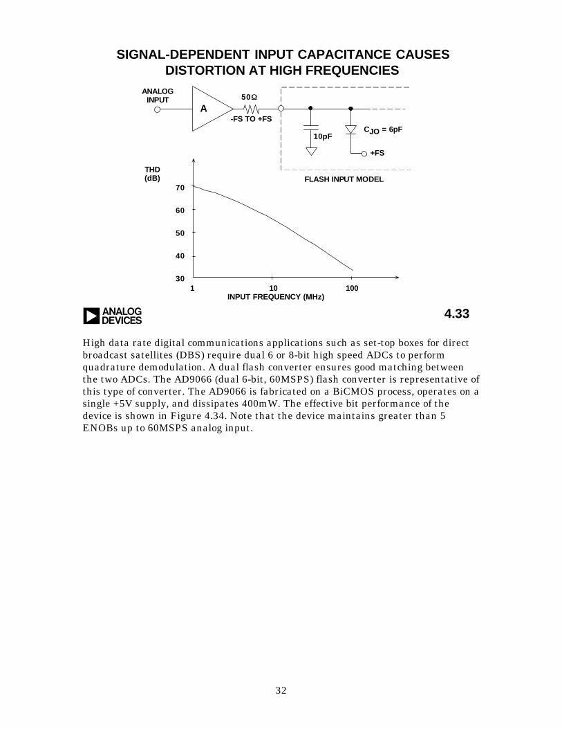
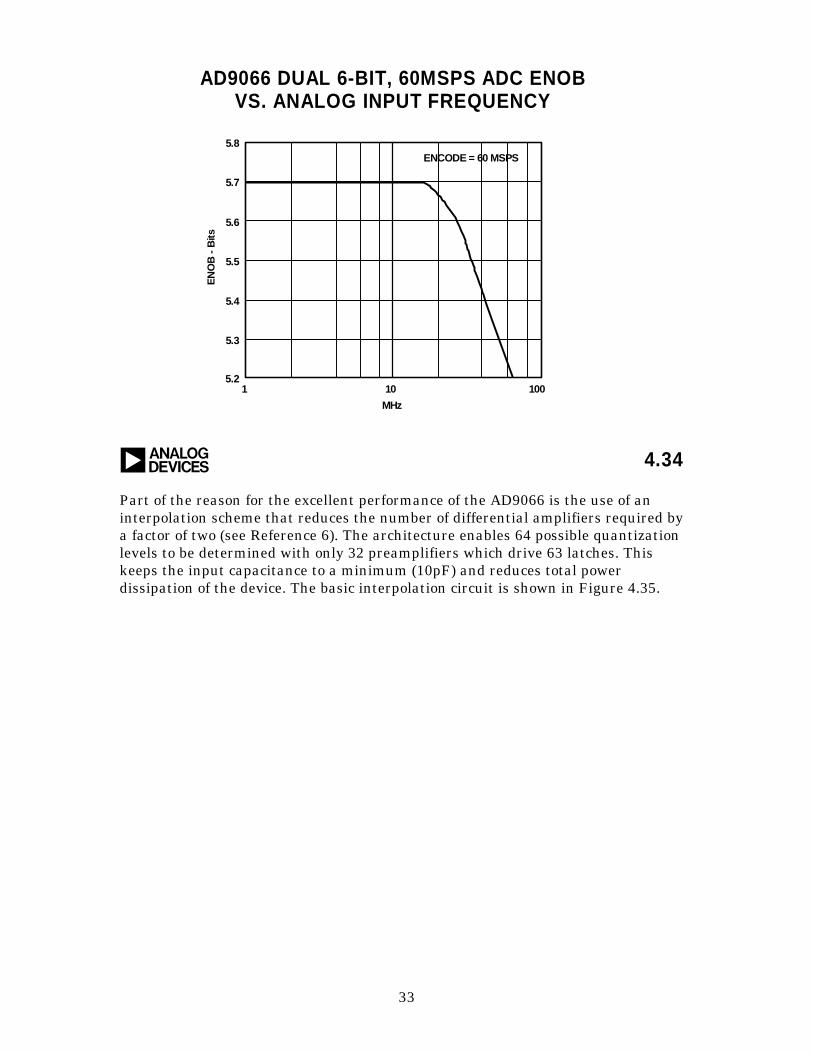
High data rate digital communications applications such as set-top boxes for directbroadcast satellites (DBS) require dual 6 or 8-bit high speed ADCs to performquadrature demodulation. A dual flash converter ensures good matching betweenthe two ADCs. The AD9066 (dual 6-bit, 60MSPS) flash converter is representative ofthis type of converter. The AD9066 is fabricated on a BiCMOS process, operates on asingle +5V supply, and dissipates 400mW. The effective bit performance of thedevice is shown in Figure 4.34. Note that the device maintains greater than 5ENOBs up to 60MSPS analog input.
33
a 4.34
AD9066 DUAL 6-BIT, 60MSPS ADC ENOBVS. ANALOG INPUT FREQUENCY
MHz
5.8
5.7
5.21 10010
5.6
5.5
5.4
5.3
ENCODE = 60 MSPS
EN
OB
- B
its
Part of the reason for the excellent performance of the AD9066 is the use of aninterpolation scheme that reduces the number of differential amplifiers required bya factor of two (see Reference 6). The architecture enables 64 possible quantizationlevels to be determined with only 32 preamplifiers which drive 63 latches. Thiskeeps the input capacitance to a minimum (10pF) and reduces total powerdissipation of the device. The basic interpolation circuit is shown in Figure 4.35.
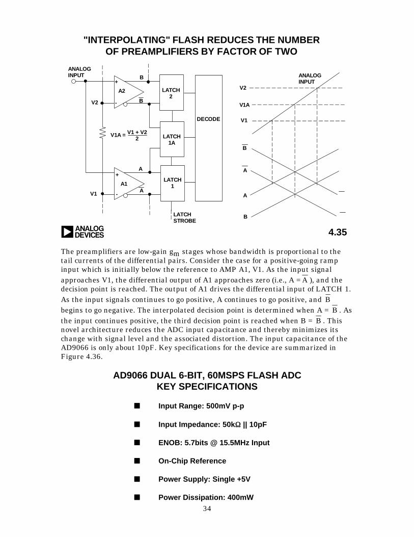
34
B
a 4.35
"INTERPOLATING" FLASH REDUCES THE NUMBEROF PREAMPLIFIERS BY FACTOR OF TWO
V1A =
A2
LATCHSTROBE
ANALOGINPUT ANALOG
INPUT
DECODE
LATCH2
LATCH1A
LATCH1
A
B
V2
V1A
A1
+
+
-
-
B
B
V1A
V1
A
A
V2
V1 + V22
The preamplifiers are low-gain gm stages whose bandwidth is proportional to thetail currents of the differential pairs. Consider the case for a positive-going rampinput which is initially below the reference to AMP A1, V1. As the input signalapproaches V1, the differential output of A1 approaches zero (i.e., A = A ), and thedecision point is reached. The output of A1 drives the differential input of LATCH 1.As the input signals continues to go positive, A continues to go positive, and Bbegins to go negative. The interpolated decision point is determined when A = B . Asthe input continues positive, the third decision point is reached when B = B . Thisnovel architecture reduces the ADC input capacitance and thereby minimizes itschange with signal level and the associated distortion. The input capacitance of theAD9066 is only about 10pF. Key specifications for the device are summarized inFigure 4.36.
AD9066 DUAL 6-BIT, 60MSPS FLASH ADCKEY SPECIFICATIONS
nn Input Range: 500mV p-p
nn Input Impedance: 50kΩΩ || 10pF
nn ENOB: 5.7bits @ 15.5MHz Input
nn On-Chip Reference
nn Power Supply: Single +5V
nn Power Dissipation: 400mW
35
nn Package: 28-pin SOIC
nn Ideal for Quadrature Demodulation
a 4.36
Subranging (Pipelined) ADCs
Although it is not practical to make flash ADCs with high resolution, flash ADCs areoften used as subsystems in "subranging" ADCs (sometimes known as "half-flashADCs"), which are capable of much higher resolutions (up to 16-bits).
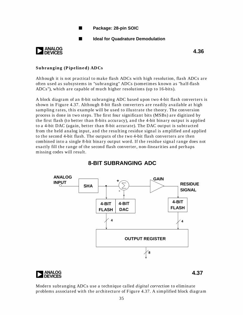
A block diagram of an 8-bit subranging ADC based upon two 4-bit flash converters isshown in Figure 4.37. Although 8-bit flash converters are readily available at highsampling rates, this example will be used to illustrate the theory. The conversionprocess is done in two steps. The first four significant bits (MSBs) are digitized bythe first flash (to better than 8-bits accuracy), and the 4-bit binary output is appliedto a 4-bit DAC (again, better than 8-bit accurate). The DAC output is subtractedfrom the held analog input, and the resulting residue signal is amplified and appliedto the second 4-bit flash. The outputs of the two 4-bit flash converters are thencombined into a single 8-bit binary output word. If the residue signal range does notexactly fill the range of the second flash converter, non-linearities and perhapsmissing codes will result.
a
8-BIT SUBRANGING ADC
4.37
ANALOGINPUT
4
8
SHA
4-BITFLASH
4-BITDAC
4-BITFLASH
GAIN
4
+
-
RESIDUESIGNAL
OUTPUT REGISTER
Modern subranging ADCs use a technique called digital correction to eliminateproblems associated with the architecture of Figure 4.37. A simplified block diagram
36
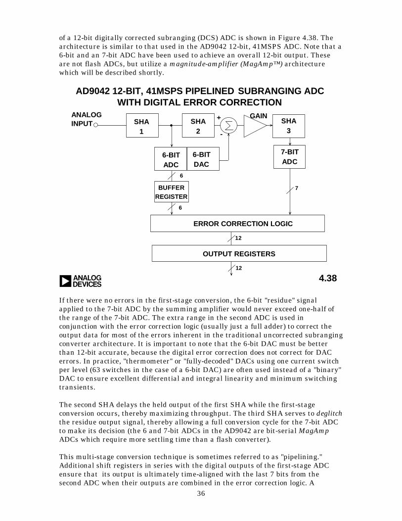
of a 12-bit digitally corrected subranging (DCS) ADC is shown in Figure 4.38. Thearchitecture is similar to that used in the AD9042 12-bit, 41MSPS ADC. Note that a6-bit and an 7-bit ADC have been used to achieve an overall 12-bit output. Theseare not flash ADCs, but utilize a magnitude-amplifier (MagAmp™) architecturewhich will be described shortly.
a
AD9042 12-BIT, 41MSPS PIPELINED SUBRANGING ADCWITH DIGITAL ERROR CORRECTION
4.38
+
-
ANALOGINPUT
7
12
ERROR CORRECTION LOGIC
OUTPUT REGISTERS
SHA1
SHA2
6-BITADC
6-BITDAC
7-BITADC
SHA3
GAIN
12
BUFFERREGISTER
6
6
If there were no errors in the first-stage conversion, the 6-bit "residue" signalapplied to the 7-bit ADC by the summing amplifier would never exceed one-half ofthe range of the 7-bit ADC. The extra range in the second ADC is used inconjunction with the error correction logic (usually just a full adder) to correct theoutput data for most of the errors inherent in the traditional uncorrected subrangingconverter architecture. It is important to note that the 6-bit DAC must be betterthan 12-bit accurate, because the digital error correction does not correct for DACerrors. In practice, "thermometer" or "fully-decoded" DACs using one current switchper level (63 switches in the case of a 6-bit DAC) are often used instead of a "binary"DAC to ensure excellent differential and integral linearity and minimum switchingtransients.
The second SHA delays the held output of the first SHA while the first-stageconversion occurs, thereby maximizing throughput. The third SHA serves to deglitchthe residue output signal, thereby allowing a full conversion cycle for the 7-bit ADCto make its decision (the 6 and 7-bit ADCs in the AD9042 are bit-serial MagAmpADCs which require more settling time than a flash converter).
This multi-stage conversion technique is sometimes referred to as "pipelining."Additional shift registers in series with the digital outputs of the first-stage ADCensure that its output is ultimately time-aligned with the last 7 bits from thesecond ADC when their outputs are combined in the error correction logic. A
37
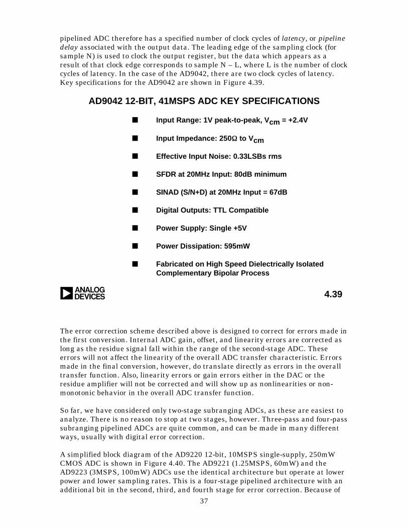
pipelined ADC therefore has a specified number of clock cycles of latency, or pipelinedelay associated with the output data. The leading edge of the sampling clock (forsample N) is used to clock the output register, but the data which appears as aresult of that clock edge corresponds to sample N – L, where L is the number of clockcycles of latency. In the case of the AD9042, there are two clock cycles of latency.Key specifications for the AD9042 are shown in Figure 4.39.
AD9042 12-BIT, 41MSPS ADC KEY SPECIFICATIONS
nn Input Range: 1V peak-to-peak, Vcm = +2.4V
nn Input Impedance: 250ΩΩ to Vcm
nn Effective Input Noise: 0.33LSBs rms
nn SFDR at 20MHz Input: 80dB minimum
nn SINAD (S/N+D) at 20MHz Input = 67dB
nn Digital Outputs: TTL Compatible
nn Power Supply: Single +5V
nn Power Dissipation: 595mW
nn Fabricated on High Speed Dielectrically IsolatedComplementary Bipolar Process
a 4.39
The error correction scheme described above is designed to correct for errors made inthe first conversion. Internal ADC gain, offset, and linearity errors are corrected aslong as the residue signal fall within the range of the second-stage ADC. Theseerrors will not affect the linearity of the overall ADC transfer characteristic. Errorsmade in the final conversion, however, do translate directly as errors in the overalltransfer function. Also, linearity errors or gain errors either in the DAC or theresidue amplifier will not be corrected and will show up as nonlinearities or non-monotonic behavior in the overall ADC transfer function.
So far, we have considered only two-stage subranging ADCs, as these are easiest toanalyze. There is no reason to stop at two stages, however. Three-pass and four-passsubranging pipelined ADCs are quite common, and can be made in many differentways, usually with digital error correction.
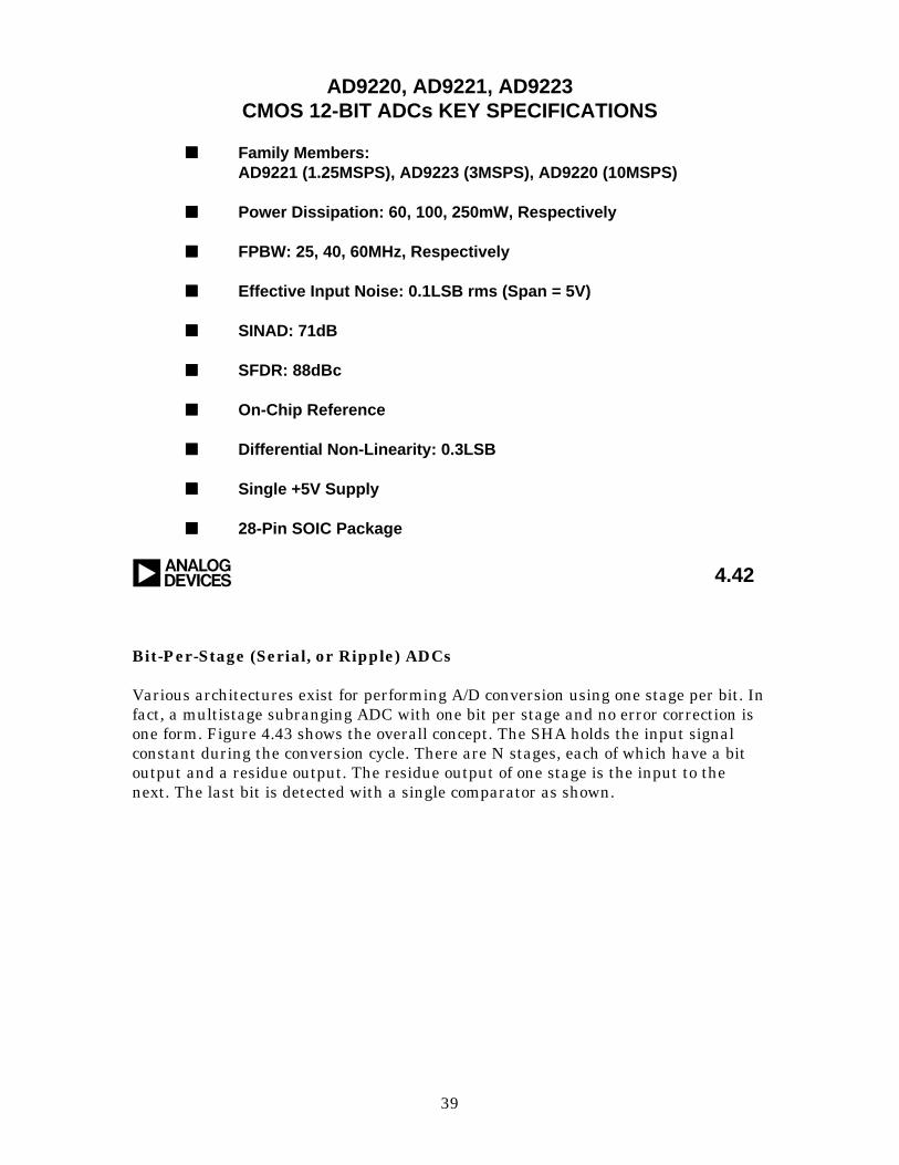
A simplified block diagram of the AD9220 12-bit, 10MSPS single-supply, 250mWCMOS ADC is shown in Figure 4.40. The AD9221 (1.25MSPS, 60mW) and theAD9223 (3MSPS, 100mW) ADCs use the identical architecture but operate at lowerpower and lower sampling rates. This is a four-stage pipelined architecture with anadditional bit in the second, third, and fourth stage for error correction. Because of
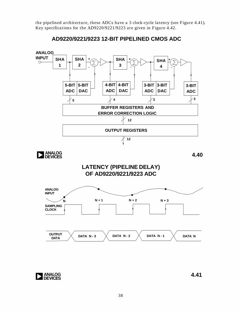
38
the pipelined architecture, these ADCs have a 3 clock-cycle latency (see Figure 4.41).Key specifications for the AD9220/9221/9223 are given in Figure 4.42.
a
AD9220/9221/9223 12-BIT PIPELINED CMOS ADC
4.40
ANALOGINPUT + + +
- - -
5 4 3 3
12
12
BUFFER REGISTERS ANDERROR CORRECTION LOGIC
OUTPUT REGISTERS
SHA1
SHA2
SHA3
SHA4
5-BITADC
5-BITDAC
4-BITADC
4-BITDAC
3-BITADC
3-BITDAC
3-BITADC
a 4.41
LATENCY (PIPELINE DELAY)OF AD9220/9221/9223 ADC
ANALOGINPUT
SAMPLINGCLOCK
OUTPUTDATA DATA N - 3 DATA N - 2 DATA N - 1 DATA N
N N + 1 N + 2 N + 3
39
AD9220, AD9221, AD9223CMOS 12-BIT ADCs KEY SPECIFICATIONS
nn Family Members:AD9221 (1.25MSPS), AD9223 (3MSPS), AD9220 (10MSPS)
nn Power Dissipation: 60, 100, 250mW, Respectively
nn FPBW: 25, 40, 60MHz, Respectively
nn Effective Input Noise: 0.1LSB rms (Span = 5V)
nn SINAD: 71dB
nn SFDR: 88dBc
nn On-Chip Reference
nn Differential Non-Linearity: 0.3LSB
nn Single +5V Supply
nn 28-Pin SOIC Package
a 4.42
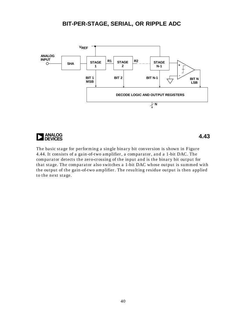
Bit-Per-Stage (Serial, or Ripple) ADCs
Various architectures exist for performing A/D conversion using one stage per bit. Infact, a multistage subranging ADC with one bit per stage and no error correction isone form. Figure 4.43 shows the overall concept. The SHA holds the input signalconstant during the conversion cycle. There are N stages, each of which have a bitoutput and a residue output. The residue output of one stage is the input to thenext. The last bit is detected with a single comparator as shown.
40
4.43
BIT-PER-STAGE, SERIAL, OR RIPPLE ADC
a
ANALOGINPUT
SHA STAGE1
STAGE2
DECODE LOGIC AND OUTPUT REGISTERS
+
-BIT 1MSB
BIT 2
VREF
N
R1 R2 STAGEN-1
BIT N-1 BIT NLSB
The basic stage for performing a single binary bit conversion is shown in Figure4.44. It consists of a gain-of-two amplifier, a comparator, and a 1-bit DAC. Thecomparator detects the zero-crossing of the input and is the binary bit output forthat stage. The comparator also switches a 1-bit DAC whose output is summed withthe output of the gain-of-two amplifier. The resulting residue output is then appliedto the next stage.
41
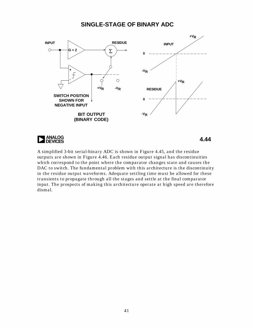
a 4.44
SINGLE-STAGE OF BINARY ADC
INPUT INPUTRESIDUE
+VR
+VR
-VR
-VR
0
0
RESIDUE+VR -VR
G = 2
+
-
Σ
BIT OUTPUT(BINARY CODE)
SWITCH POSITIONSHOWN FOR
NEGATIVE INPUT
A simplified 3-bit serial-binary ADC is shown in Figure 4.45, and the residueoutputs are shown in Figure 4.46. Each residue output signal has discontinuitieswhich correspond to the point where the comparator changes state and causes theDAC to switch. The fundamental problem with this architecture is the discontinuityin the residue output waveforms. Adequate settling time must be allowed for thesetransients to propagate through all the stages and settle at the final comparatorinput. The prospects of making this architecture operate at high speed are thereforedismal.
42
4.45
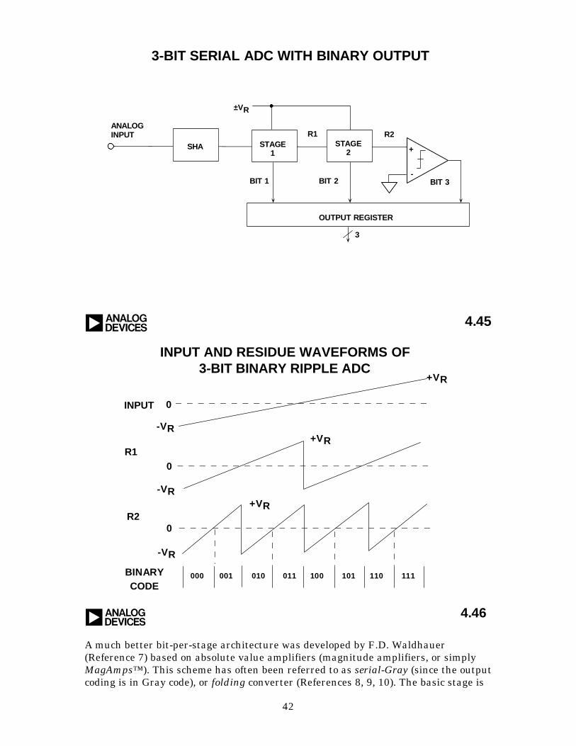
3-BIT SERIAL ADC WITH BINARY OUTPUT
a
ANALOGINPUT
SHA STAGE1
STAGE2
OUTPUT REGISTER
+
-BIT 1 BIT 2 BIT 3
±VR
3
R1 R2
a
INPUT AND RESIDUE WAVEFORMS OF3-BIT BINARY RIPPLE ADC
4.46
INPUT
R1
R2
BINARYCODE
-VR
-VR
-VR
+VR
+VR
+VR
000 001 010 011 100 101 110 111
0
0
0
A much better bit-per-stage architecture was developed by F.D. Waldhauer(Reference 7) based on absolute value amplifiers (magnitude amplifiers, or simplyMagAmps™). This scheme has often been referred to as serial-Gray (since the outputcoding is in Gray code), or folding converter (References 8, 9, 10). The basic stage is
43
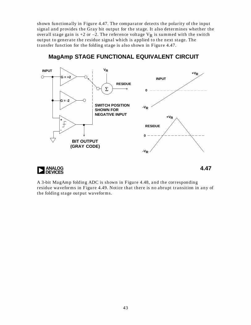
shown functionally in Figure 4.47. The comparator detects the polarity of the inputsignal and provides the Gray bit output for the stage. It also determines whether theoverall stage gain is +2 or –2. The reference voltage VR is summed with the switchoutput to generate the residue signal which is applied to the next stage. Thetransfer function for the folding stage is also shown in Figure 4.47.
a 4.47
MagAmp STAGE FUNCTIONAL EQUIVALENT CIRCUIT
INPUT
G = +2 INPUT
RESIDUE
+VR
+VR
-VR
-VR
0
0
RESIDUE
VR
+
-
BIT OUTPUT(GRAY CODE)
G = -2
Σ
SWITCH POSITIONSHOWN FORNEGATIVE INPUT
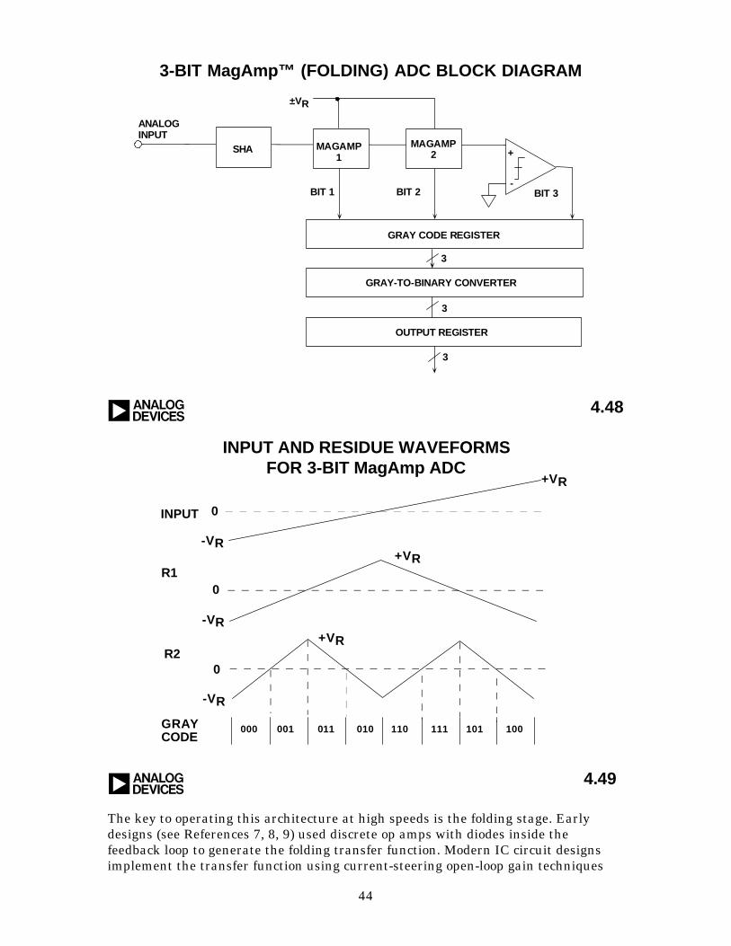
A 3-bit MagAmp folding ADC is shown in Figure 4.48, and the correspondingresidue waveforms in Figure 4.49. Notice that there is no abrupt transition in any ofthe folding stage output waveforms.
44
4.48
3-BIT MagAmp™ (FOLDING) ADC BLOCK DIAGRAM
a
ANALOGINPUT
SHA MAGAMP1
MAGAMP2
GRAY-TO-BINARY CONVERTER
OUTPUT REGISTER
GRAY CODE REGISTER
+
-BIT 1 BIT 2 BIT 3
±VR
3
3
3
a
INPUT AND RESIDUE WAVEFORMSFOR 3-BIT MagAmp ADC
4.49
INPUT
R1
R2
GRAYCODE
-VR
-VR
-VR
+VR
+VR
+VR
000 001 011 010 110 111 101 100
0
0
0
The key to operating this architecture at high speeds is the folding stage. Earlydesigns (see References 7, 8, 9) used discrete op amps with diodes inside thefeedback loop to generate the folding transfer function. Modern IC circuit designsimplement the transfer function using current-steering open-loop gain techniques
45
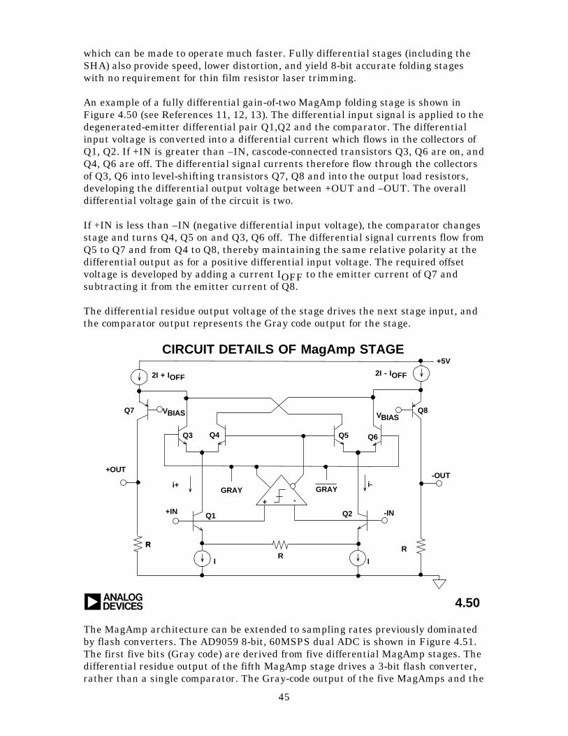
which can be made to operate much faster. Fully differential stages (including theSHA) also provide speed, lower distortion, and yield 8-bit accurate folding stageswith no requirement for thin film resistor laser trimming.
An example of a fully differential gain-of-two MagAmp folding stage is shown inFigure 4.50 (see References 11, 12, 13). The differential input signal is applied to thedegenerated-emitter differential pair Q1,Q2 and the comparator. The differentialinput voltage is converted into a differential current which flows in the collectors ofQ1, Q2. If +IN is greater than –IN, cascode-connected transistors Q3, Q6 are on, andQ4, Q6 are off. The differential signal currents therefore flow through the collectorsof Q3, Q6 into level-shifting transistors Q7, Q8 and into the output load resistors,developing the differential output voltage between +OUT and –OUT. The overalldifferential voltage gain of the circuit is two.
If +IN is less than –IN (negative differential input voltage), the comparator changesstage and turns Q4, Q5 on and Q3, Q6 off. The differential signal currents flow fromQ5 to Q7 and from Q4 to Q8, thereby maintaining the same relative polarity at thedifferential output as for a positive differential input voltage. The required offsetvoltage is developed by adding a current IOFF to the emitter current of Q7 andsubtracting it from the emitter current of Q8.
The differential residue output voltage of the stage drives the next stage input, andthe comparator output represents the Gray code output for the stage.
VBIAS
Q4
Q7
a 4.50
CIRCUIT DETAILS OF MagAmp STAGE
+OUT
+5V
Q8
-OUT
R
-IN+IN
R
RII
Q6Q5Q3
Q1
GRAY GRAY
Q2
R
i+ i-
VBIAS
2I + IOFF 2I - IOFF
+ -
The MagAmp architecture can be extended to sampling rates previously dominatedby flash converters. The AD9059 8-bit, 60MSPS dual ADC is shown in Figure 4.51.The first five bits (Gray code) are derived from five differential MagAmp stages. Thedifferential residue output of the fifth MagAmp stage drives a 3-bit flash converter,rather than a single comparator. The Gray-code output of the five MagAmps and the
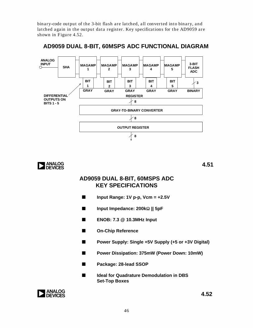
46
binary-code output of the 3-bit flash are latched, all converted into binary, andlatched again in the output data register. Key specifications for the AD9059 areshown in Figure 4.52.
4.51
AD9059 DUAL 8-BIT, 60MSPS ADC FUNCTIONAL DIAGRAM
a
8
8
8
ANALOGINPUT
SHA MAGAMP1
MAGAMP2
MAGAMP3
MAGAMP4
MAGAMP5
3-BITFLASH
ADC
BIT1
GRAY
BIT2
GRAY
BIT3
GRAY
BIT4
GRAY
BIT5
GRAY
3
GRAY-TO-BINARY CONVERTER
OUTPUT REGISTER
BINARYDIFFERENTIALOUTPUTS ONBITS 1 - 5
REGISTER
AD9059 DUAL 8-BIT, 60MSPS ADCKEY SPECIFICATIONS
nn Input Range: 1V p-p, Vcm = +2.5V
nn Input Impedance: 200kΩΩ || 5pF
nn ENOB: 7.3 @ 10.3MHz Input
nn On-Chip Reference
nn Power Supply: Single +5V Supply (+5 or +3V Digital)
nn Power Dissipation: 375mW (Power Down: 10mW)
nn Package: 28-lead SSOP
nn Ideal for Quadrature Demodulation in DBSSet-Top Boxes
a 4.52

47
48
REFERENCES
1. Active and Passive Electrical Wave Filter Catalog, Vol. 34, TTE,Incorporated, 2251 Barry Avenue, Los Angeles, CA 90064.
2. W. R. Bennett, “Spectra of Quantized Signals”, Bell System TechnicalJournal, No. 27, July 1948, pp. 446-472.
3. Steve Ruscak and Larry Singer, Using Histogram Techniques toMeasure A/D Converter Noise, Analog Dialogue, Vol. 29-2, 1995.
4. M.J. Tant, The White Noise Book, Marconi Instruments, July 1974.
5. G.A. Gray and G.W. Zeoli, Quantization and Saturation Noise dueto A/D Conversion, IEEE Trans. Aerospace and ElectronicSystems, Jan. 1971, pp. 222-223.
6. Chuck Lane, A 10-bit 60MSPS Flash ADC, Proceedings of the 1989Bipolar Circuits and Technology Meeting, IEEE Catalog No.89CH2771-4, September 1989, pp. 44-47.
7. F.D. Waldhauer, Analog to Digital Converter, U.S. Patent3-187-325, 1965.
8. J.O. Edson and H.H. Henning, Broadband Codecs for an Experimental224Mb/s PCM Terminal, Bell System Technical Journal, 44,November 1965, pp. 1887-1940.
9. J.S. Mayo, Experimental 224Mb/s PCM Terminals, Bell SystemTechnical Journal, 44, November 1965, pp. 1813-1941.
10. Hermann Schmid, Electronic Analog/Digital Conversions,Van Nostrand Reinhold Company, New York, 1970.
11. Carl Moreland, An 8-bit 150MSPS Serial ADC, 1995 ISSCC Digestof Technical Papers, Vol. 38, p. 272.
12. Roy Gosser and Frank Murden, A 12-bit 50MSPS Two-Stage A/DConverter, 1995 ISSCC Digest of Technical Papers, p. 278.
13. Carl Moreland, An Analog-to-Digital Converter Using Serial-Ripple Architecture, Masters' Thesis, Florida State UniversityCollege of Engineering, Department of Electrical Engineering, 1995.
14. Practical Analog Design Techniques, Analog Devices, 1995, Chapter4, 5, and 8.
15. Linear Design Seminar, Analog Devices, 1995, Chapter 4, 5.
16. System Applications Guide, Analog Devices, 1993, Chapter 12, 13,15,16.
49
17. Amplifier Applications Guide, Analog Devices, 1992, Chapter 7.
18. Walt Kester, Drive Circuitry is Critical to High-Speed Sampling ADCs,Electronic Design Special Analog Issue, Nov. 7, 1994, pp. 43-50.
19. Walt Kester, Basic Characteristics Distinguish Sampling A/D Converters,EDN, Sept. 3, 1992, pp. 135-144.
20. Walt Kester, Peripheral Circuits Can Make or Break Sampling ADCSystems, EDN, Oct. 1, 1992, pp. 97-105.
21. Walt Kester, Layout, Grounding, and Filtering Complete SamplingADC System, EDN, Oct. 15, 1992, pp. 127-134.
22. Robert A. Witte, Distortion Measurements Using a Spectrum Analyzer,RF Design, September, 1992, pp. 75-84.
23. Walt Kester, Confused About Amplifier Distortion Specs?, AnalogDialogue, 27-1, 1993, pp. 27-29.
24. System Applications Guide, Analog Devices, 1993, Chapter 16.
25. Frederick J. Harris, On the Use of Windows for Harmonic Analysiswith the Discrete Fourier Transform, IEEE Proceedings, Vol. 66, No. 1,Jan. 1978, pp. 51-83.
26. Joey Doernberg, Hae-Seung Lee, David A. Hodges, Full Speed Testingof A/D Converters, IEEE Journal of Solid State Circuits, Vol. SC-19,No. 6, Dec. 1984, pp. 820-827.
27. Brendan Coleman, Pat Meehan, John Reidy and Pat Weeks, CoherentSampling Helps When Specifying DSP A/D Converters, EDN, October 15,1987, pp. 145-152.
28. Robert W. Ramierez, The FFT: Fundamentals and Concepts,Prentice-Hall, 1985.
29. R. B. Blackman and J. W. Tukey, The Measurement of PowerSpectra, Dover Publications, New York, 1958.
30. James J. Colotti, Digital Dynamic Analysis of A/D ConversionSystems Through Evaluation Software Based on FFT/DFT Analysis,RF Expo East 1987 Proceedings, Cardiff Publishing Co., pp. 245-272.
31. HP Journal, Nov. 1982, Vol. 33, No. 11.
32. HP Product Note 5180A-2.
33. HP Journal, April 1988, Vol. 39, No. 2.
34. HP Journal, June 1988, Vol. 39, No. 3.
50
35. Dan Sheingold, Editor, Analog-to-Digital Conversion Handbook,Third Edition, Prentice-Hall, 1986.
36. Lawrence Rabiner and Bernard Gold, Theory and Application ofDigital Signal Processing, Prentice-Hall, 1975.
37. Matthew Mahoney, DSP-Based Testing of Analog and Mixed-SignalCircuits, IEEE Computer Society Press, Washington, D.C., 1987.
38. IEEE Trial-Use Standard for Digitizing Waveform Recorders,No. 1057-1988.
39. Richard J. Higgins, Digital Signal Processing in VSLI, Prentice-Hall,1990.
40. M. S. Ghausi and K. R. Laker, Modern Filter Design: Active RC andSwitched Capacitors, Prentice Hall, 1981.
41. Mathcad™ 4.0 software package available from MathSoft, Inc.,201 Broadway, Cambridge MA, 02139.
42. Howard E. Hilton, A 10MHz Analog-to-Digital Converter with 110dBLinearity, H.P. Journal, October 1993, pp. 105-112.