thermo-mechanical simulation and optimization …
TRANSCRIPT

THERMO-MECHANICAL SIMULATION AND OPTIMIZATION ANALYSIS FOR WARPAGE-INDUCED PBGA SOLDER JOINT FAILURES
Caiying He, Ph.D., Zuyao Liu, Hongxia Wang, Lei Wang, Feng Lu, Ph.D., and Hongfeng Ran
Kaifa Technology Shenzhen, Guangdong, P. R. China
[email protected] and [email protected] ABSTRACT In SMT assembly process, the thermal warpage becomes one of the root causes of solder joint reliability failures for PBGA. The accurate prediction for warpage of PBGA and PCB is an important and challenging task of numerical simulation of PBGA solder joint defect. In this paper, the numerical analysis of warpage in PBGA and PCBA is carried out in consideration of the residual stresses produced during SMT reflow process. The analysis methodology using a viscoelastic based material model is adopted to account the time and temperature dependent behavior of an epoxy molding compound. In order to get a series of material constant for Generalized Maxwell Viscoelastic Model, DMA (Dynamic Mechanical Analyzer) tests for mold compound material sample is performed to generate viscoelastic material relaxation function through curve fitting. The experimental research on thermo warpage at different temperature for both PBGA and assembled PCBA is carried out by using the Shadow Morie method. The experimental data is compared with the simulation results as verification for FEA modeling. It is found that the predictions are in agreement with experimental data, especially in qualitative analysis. Optimization analysis is also performed to study the effect of PBGA material properties, molding curing temperature and SMT process parameters on warpage and solder joint failures. Key words: PBGA, FEA, warpage, DMA, viscoelastic, EMC, CTE, residue stress, reflow process INTRODUCTION The trend of electronic products is moving toward further miniaturization and improved performance. The continuous drive toward high density and low profile integrated circuit packaging has led to the growing application of different package types, i.e. Plastic-ball-grid-array (PBGA), chip-scale-package (CSP) and flip-chip-on-board (FCOB) assemblies etc... Epoxy molding compound (EMC) is the basic material for most of the electronic components and chip packages. Hence, it is necessary to understand the thermo-mechanical material properties of EMC and its applications in Microelectronic Industry. An area-array package which is molded only on one side
often shows warpage when it is cooled down to room temperature after molding due to the CTE (Coefficient of Thermal Expansion) mismatch between the substrate and the EMC. The package warpage leads to reliability deterioration of the connection between the circuit board and the solder bumps. As an example of typical package level material for thermo-mechanical performance study, PBGA is chosen for Finite Element Analysis (FEA) modeling to understand the warpage and residue stress after reflow in this paper. PBGA manufacturers and customers are increasingly paying attention to PBGA warpage, which becomes a determining quality criterion for parts acceptance. Due to thermal expansion mismatch between the microelectronics package and the printed circuit board on which the package is mounted, thermal stress is introduced in the cooling phase of solder assembly process. Dynamic stress is further produced in the completed package-board assembly, especially in the solder joints, when the assembly is subjected to power cycling, thermal cycling, or thermal shock. The dynamic stress/strain has a great impact on the long-term reliability of the solder joint. Figure 1 is a typical picture of the solder joint failure due to the warpage of PBGA. In this paper, the study of warpage distribution and residue stress of PBGA assembled on PCB during the reflow process are discussed. Package warpage during the cooling process just after the molding is also one of the critical issues in the manufacturing of PBGA packaging3,4. Such warpage depends on the epoxy molding compound characteristics and the dimensional details of the PBGA package design. The effect of the curing process and dimensional package design on warpage will not be included in this study, which would be discussed in future work. Finite Element Method (FEM) is a powerful tool to analyze the PBGA characteristics involved in variations of the material properties, such as material moduli and CTE of the mold compound, substrate and silicon die, to determine their effects on the package warpage. Package material selection and assembly process conditions should be optimized to minimize the package warpage and residual stress. In general, the elastic model is used to model the polymeric behavior and thus captures only the final state of the warpage approximately5. This paper
As originally published in the SMTA International Conference Proceedings.

Crack
100X PCB Pad
provides detailed study using viscoelastic model enabling us to take into account the process history and the glass transition effects of the molding compound, which affects the warpage of assembled product.
Figure 1. A Typical Soldering Crack Failure and Cross Section of Defective PBGA
VISCOELASTIC BEHAVIOR OF EPOXY MOLDING COMPOUND A thermorheologically simple model of viscoelastic material is introduced to consider the stress relaxation effect and to describe the dynamic mechanical behavior of the EMC versus temperature changes. Epoxy molding compound’s stiffness behavior is more similar to a viscoelastic material rather than a typical behavior of elastic material. In simplified terms, these materials behave in between the elastic-solid and the Newtonian- liquid, where the former undergoes a constant strain under a constant applied stress and the latter undergoes a constant-rate of strain under the same constant applied stress. These two states of material are well represented by a spring and dashpot system in imitating elastic and viscous material behaviors. The viscoelastic material’s time dependent behavior can be mathematically represented using theoretical and experimental means.
Figure 2. Generalized Maxwell Model These models can be constructed using springs and dashpots in series and parallel combinations. Figure 2 is a Generalized Maxwell model for the stress relaxation behavior of polymeric materials, which expresses a more accurate mathematical model with a spectrum of Maxwell elements with different relaxation time constant i ranging over a time decade, as follows6-8:
n
i
ti
ieEEtE1
/)( (1)
where E(t) is the tensile relaxation function. E∞ is the steady state value and Ei and
iii E are the individual modulus and time constant of each Maxwell elements among the ‘n’ such elements. The short term modulus E0 (Et = 0) is given by:
n
iiEEE
10 (2)
Based on small deformation theory, the constitutive equation for an isotropic viscoelastic material can be written as:
tt
dd
dtKId
d
detG
00)()(2
(3)
where: = Cauchy stress e = deviatoric part of the strain = volumetric part of the strain
…
G(t) = shear relaxation kernel function K(t) = bulk relaxation kernel function En E1 E2 t = current time
E = past time I = unit tensor
ηn η1 η2 For the element SOLID185 in ANSYS, the kernel functions are represented in terms of Prony series, which assumes that:
G Gi
n
i
tieGGtG
1
/)(
(4)
K Ki
n
i
tieKKtK
1
/)( (5)
where , are the shear relaxation modulus and bulk relaxation modulus. and are the relaxation times for each Prony component corresponding to shear and bulk relaxation functions.
iG iKGi
Ki
As originally published in the SMTA International Conference Proceedings.

Young’s complex modulus can be directly measured in DMA by the three-point-bending method. ANSYS FEM usually requires input of the shear relaxation function and bulk relaxation function with time. Assuming that the instantaneous Poisson’s ratio of EMC is a constant and the instantaneous terms (Young’s modulus, shear, and bulk moduli) relate with each other through an elastic relationship in below Equations (6), the instantaneous shear and bulk moduli can be calculated.
)21(3
)1(2
EK
EG
(6)
where is the Poisson ratio. Among the various curve-fitting techniques, the Prony Series form9 for the relaxation modulus, as shown earlier in Equation (1) using ‘n’ Maxwell elements (see Figure 2), is commonly used for most finite element packages. Introducing the relative moduli:
0GGiG
i , 0KKi
Ki (7)
where:
Gn
iiGGG
10
, (8)
Kn
iiKKK
10
The kernel functions can be equivalently expressed as:
G Gi
n
i
tGi
G eGtG1
/0)( (9)
K Ki
n
i
tKi
K eKtK1
/0)( (10)
The integral function (Equation 3) can recover the elastic behavior at the limits of very slow and very fast loads. Here, G and K are the moduli at the slow limit. The elasticity parameters input correspond to those of the fast load limit. The Time-Temperature equivalency principle can be used for the linear viscoelastic stress-strain behavior5. The deformational behavior of viscoelastic materials to an applied stress is dependent on both temperature and time. The time factor can be seen in terms of the rate of loading, load magnitude and load duration. The temperature dependence is influenced by the thermal properties of the epoxy. In linear viscoelastic nature, the time and temperature dependence of the relationship between stress and strain is superposable and therefore essentially equivalent. The effect of time and temperature-dependent viscoelastic properties can be examined experimentally by DMA, which is explained in the forthcoming paragraphs.
In order to compare the effect of viscoelastic nature on warpage, an elastic model for EMC is also included in the analysis. DMA TEST FOR VISCOELASTIC RELAXATION MODULUS DMA is found to be suitable to evaluate the viscoelastic properties of the material5,8. The method involves in holding the EMC sample by the three-point-bending method and applying a sinusoidal force or strain. This results in a bending deformation of the sample which varies sinusoidally with time. Since frequency is the inverse of time variable, the experiment can be scanned under a continuous frequency range (e.g., 0.01 to 100 Hz). The viscoelastic effect of the EMC causes a time lag between the applied stress and resultant strain, hence the ratio of stress and strain results as a complex number. The real part is called the storage modulus and the imaginary part is called the loss modulus. The storage modulus relates to the amount of recoverable energy stored within a deformed material (solid-like behavior) while the loss modulus relates to the amount of unrecoverable energy lost within a deformed material (fluid-like behavior). Experimentally, the material characterization of the EMC involves the determination of the relaxation data at various temperatures and frequencies (Figure 3). This is obtained from a DMA experiment and is further used in forming a master curve by rigid horizontal shifting of individual curves along the logarithmic time axis to some arbitrary reference temperature (Tr) curve. Researchers have come out with various forms of horizontal shift function A(T), William-Landel-Ferry (WLF) model, Arrhenius and other empirical models5,8. Among them the WLF model (Equation 11) is the most commonly used for the EMC hence adopted for the present study.
)(
)())((
2
1
r
r
TTC
TTCTALog
(11)
St
orag
e M
odul
us (
MP
a)
Los
s M
odul
us (
MP
a)
For EMCs, the constants C1 and C2 can also be obtained from DMA test, while the reference temperature is
Figure 3. Complex Modulus curves with temperature at different frequencies.
Temp. (℃)
As originally published in the SMTA International Conference Proceedings.

maintained close to the mold temperature, which is the stress free temperature at 180℃, i.e. just equal to the ultimate glass transition temperature Tg = 180℃. The results from proper shifted relaxation curves in DMA software give to a smooth fit master curve, which reflects the dependence of both temperature and frequency.
(Pa
)
(s)
Figure 4. Master curve for Relaxation Function When the complex moduli are transformed to relaxation function. The curve fitting result of Relaxation function is shown in Figure 4, which is obtained by MATLAB program and curve fitting technique in ANSYS. The relative shear relaxation modulus and relative bulk relaxation modulus
i, and the shear and bulk
relaxation times and are listed in table 1.
G Ki
Ki
Gi
Table 1. Curve Fitting Result of Relaxation Function for EMC DMA Test
n Gi G
i Ki K
i
1 0.1354 1.892E-03 0.1353 1.888E-03
2 0.2005 5.003E-02 0.2005 4.994E-02
3 0.1895 8.449E-01 0.1896 8.436E-01
4 0.1450 1.240E+01 0.1450 1.238E+01
5 0.0996 1.797E+02 0.0996 1.795E+02
6 0.0648 2.769E+03 0.0648 2.765E+03
7 0.0399 4.941E+04 0.0399 4.933E+04
8 0.0224 1.211E+06 0.0224 1.210E+06
9 0.0126 6.540E+07 0.0126 6.535E+07
G0 1.000E+10 K0 1.750E+10 G 0.0904
K 0.0904
FEA SIMULATION FOR PBGA WARPAGE Geometry Model A three-dimensional FEA model of the PBGA assembly is created as shown in Figure 5. Due to its symmetry, only half of the PBGA assembly is modeled using ANSYS program. A strip 3D model is more convenient for easier convergence of complicated nonlinear calculations. The EMC, silicon die, solder joints, substrate and PCB have
thicknesses in mm of 1.17, 0.3, 0.5, 0.56 and 1.0, respectively.
a) 1/2 model; b) Strip model; c) Symmetry section. Figure 5. PBGA Simulation Geometry Models.
FEM Model and Material Properties Silicon die is modeled as isotropic temperature dependent, while BT substrate and FR-4 PCB are modeled as orthotropic temperature dependent materials. The EMC exhibits significant time-temperature dependent viscoelastic behavior which is modeled with the generalized Maxwell’s elements whose model parameters is obtained from the actual DMA test mentioned above. Their elastic properties have been summarized in Table 2-410-12, which are mostly obtained from product data sheets. Solder joints are assumed to exhibit viscoplastic behavior. The Elastic modulus of the solder is assumed to be temperature dependent given by table 4. The reference temperatures for all the materials are fixed at their processing/curing temperatures. Thus, the reference temperatures are 25°C for die, 180°C for EMC and BT substrate, 143°C for FR-4 board and 217°C for solder joints.
Viscoplastic Material Model for Solder Joints Anand’s model and Garofalo-Arrhenius model for vicsoplastic material properties are prescribed using ANSYS element type of Visco107 and Solid 185 to account for the nonlinear creep behavior of the solder joints9-13. Due to convergence issue for large-deformation Anand’s model, the Garofalo-Arrhenius is adopted in this paper.
RT
QA n
p expsinh (12)
Where pis equivalent creep strain rate ( );
1s is
PCB Solder joints Substrate Silicon Die EMC
Z
Y
X
a)
c)
b)
Z
Y
X
Z
X
As originally published in the SMTA International Conference Proceedings.
equivalent von Mises stress (Gpa); T is absolute temperature (kelvin). Q/R is the activation energy. Parameters for near-eutectic 95.5Sn/3.8Ag/0.7Cu are given in Table 5 14. Table 2. Material Properties for Those Modeled as Temperature Independent. Material CTE
(ppm/℃)
α1/α2
E (GPa)
(<Tg)/
(>Tg)
G (GPa)
(<Tg)/
(>Tg)
Ref.
Temp.
(℃)
Die Table 3 Table 3 - 0.28 25
Solder Joints 20 Table 4 - 0.36 217
EMC (Tg = 180℃) 8/28 27/1.8 - 0.26 180 x axis 15/5 24/17 6/2.4 y axis 15/5 24/17 6/2.4
Substrate
(Tg = 180℃) z axis 50/220 8.3/5.2 6.2/2.6
0.18 180
x axis 15/58 24/17 6/2.4 y axis 13/58 24/17 6/2.4
FR-4
(Tg = 143℃) z axis 45/221 8.3/5.2 6.2/2.6
0.18 143
Table 3. Mechanical Properties of Silicon Die (temperature dependent)
Temp(�) 20 27 127 227 250
E (GPa) 130.0 130.0 129.1 128.2 128.2
CTE (ppm/�) 2.56 2.58 3.11 3.11 3.11
Table 4. Mechanical Properties of Solder Joints (Sn3.8Ag0.7Cu, temperature dependent)
Temp (�) 25 50 75 100 125 150
E (GPa) 43.6 42.2 40.8 39.3 37.9 36.5 Temp (�) 175 200 215 217 225 250 E (GPa) 35.0 33.6 32.7 1e-5 1e-5 1e-5
Table 5. Viscoplastic Model Parameters for Solder Joints.
Definition Denote Unit 3.8Ag0.7Cu
Exponential factor A 1/s 926(508-T)/T
Stress coefficient - (37.78 106-74,414T)-1
Strain rate sensitivity of stress n - 3.3
Activation energy Q/R K 6360
Temperature Loads and Boundary Conditions Linear elastic material model solution for whole PBGA and PCB assembly is easily convergent when going through reflow process, but nonlinear (either visco-elastic or visco-plastic) material model solution is difficult to converge due to large calculation scale to meet dense solder joints meshing. Hence, besides the whole PBGA and PCB model for linear elastic material simulation, a simplified strip symmetric FEM model including one row of solder joints in Figure 5(b) is also adopted to complete the viscoelastic and viscoplastic analysis for the whole reflow temperature profile loadings. The reflow temperature profile is shown in Figure 6, which specifies the temperature ramp up from room temperature to 240 oC
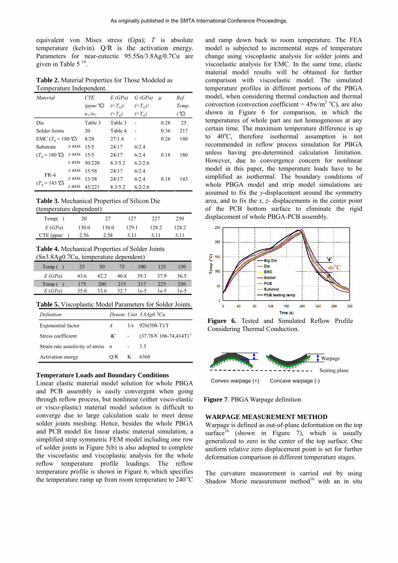
and ramp down back to room temperature. The FEA model is subjected to incremental steps of temperature change using viscoplastic analysis for solder joints and viscoelastic analysis for EMC. In the same time, elastic material model results will be obtained for further comparison with viscoelastic model. The simulated temperature profiles in different portions of the PBGA model, when considering thermal conduction and thermal convection (convection coefficient = 45w/m2 oC), are also shown in Figure 6 for comparison, in which the temperatures of whole part are not homogeneous at any certain time. The maximum temperature difference is up to 40oC, therefore isothermal assumption is not recommended in reflow process simulation for PBGA unless having pre-determined calculation limitation. However, due to convergence concern for nonlinear model in this paper, the temperature loads have to be simplified as isothermal. The boundary conditions of whole PBGA model and strip model simulations are assumed to fix the y-displacement around the symmetry area, and to fix the x, z- displacements in the center point of the PCB bottom surface to eliminate the rigid displacement of whole PBGA-PCB assembly.
Figure 6. Tested and Simulated Reflow ProfileConsidering Thermal Conduction.
40 oC
Seating plane
Warpage
Convex warpage (+) Concave warpage (-)
Figure 7. PBGA Warpage definition WARPAGE MEASUREMENT METHOD Warpage is defined as out-of-plane deformation on the top surface16 (shown in Figure 7), which is usually generalized to zero in the center of the top surface. One uniform relative zero displacement point is set for further deformation comparison in different temperature stages. The curvature measurement is carried out by using Shadow Morie measurement method16 with an in situ
As originally published in the SMTA International Conference Proceedings.

heating chamber. The fringe pattern is a displacement contour of out-of-plane deformation on the sample surface, which is similar as simulation deformation contour. A typical fringe pattern of the PBGA warpage is shown in Figure 8. The experiment proves that the deformation of the sample is indeed near to an axisymmetric spherical surface.
Figure 8. Measured Warpage in 3D Display
RESULTS ANALYSIS Deformation trend of elastic material 1/2 model under isothermal assumption is shown in Figure 9, which shows 2 maximum deformations, one at 240 oC during the ramp up (heating) process while the other occurs at 200 oC during the ramp down (cooling) process. The former is a convex warpage while the latter is a concave warpage, which is observed in most of our experiment results for PBGA with different kinds of EMC materials, as shown in Figure 10. It is noticed that simulation warpage values are calculated from whole EMC body deformation, instead of from top surface only, which are definitely equal or larger than actual values. Dash line is the FEA result from 1/2 model, which is shifted from concave to more convex compared to tested warpage value for currently used PBGA (the model in this paper). The reason of this shift is that the assumed reference temperature of the EMC and BT substrate, which is 180oC for zero stress state, may not be the actual molding temperature. Usually, the molding temperature is set as the reference temperature of PBGA packaging. Another observation is the CTE of substrate above Tg (180 oC) is 5ppm/ oC only, which is much less than EMC CTE of 28ppm/ oC at same temperature range. It will cause the convex warpage shape in higher temperature. However, the CTE measured from the Shadow Morie method is 19ppm/ oC on the bottom side of PBGA, i.e. substrate layer, which is much higher than substrate CTE in data sheet. Hence the substrate data sheet may give a very rough value of CTE instead.
Figure 9. Warpage Contour during Reflow Temperature Cycle
-300-250-200-150
-100-50
050
100150
200250300350
20 100 183 220 240 260 240 217 183 100 20
Temp (℃)
War
pag
e (
µm
)
Currently Used EMC A EMC BEMC C EMC D EMC EFEA -PBGA FEA -BGA+PCB
Figure 10. Experiment Warpage Comparison for PBGA with Different Epoxy Mold Compound.
Warpages at Different Reference Temperatures
-800
-700
-600
-500
-400
-300
-200
-100
0
100
200
300
153 183 220 240
Temp (℃)
War
page
( µ
m)
Actual test for PBGA alone
Ref: Tref = 180℃ for EMC, BT
Tref =225℃ for EMC, BT
Tref =188℃ for FR-4
Tref =25℃ for FR-4
Figure 11. Warpages Comparison for Different Reference Temperatures in Components. Reference temperature is an important parameter for thermal analysis simulation in ANSYS, which is defined as zero stress temperature in certain component. In this study, since some process conditions are unknown, the assumption of reference temperatures for each component in the ANSYS model is needed. A warpage comparison for different reference temperature for various components in the model has been done. Each run only changes one or two reference temperatures, while other parameters maintain with original values in table 2. As we
As originally published in the SMTA International Conference Proceedings.
predicted, the significant differences among all assumptions are found, shown in Figure 11. Especially when reference temperature of FR-4 is 25 oC, the maximum warpage could be 725m. The simulated internal stresses also show significant differences, which is not presented here. From the reference temperature comparison result, it is critical to understand the process flow and conditions of packages molding before starting simulation work and obtain closure with experimental data.
The warpage results for strip model are shown in Figure 12. The simulation results under full elastic condition, viscoelastic EMC condition and viscoelastic EMC plus viscoplastic solder joints condition have same deformation patterns, which are concave at 183 oC and 200 oC, while being convex below 100 oC and above 220oC. This pattern is also similar with whole 1/2 model results. The only difference is that the warpage for 1/2 model is at PBGA’s diagonal direction, while in the strip model it is along with x axis at y = 0. Usually the former is larger than the latter. For quantitative comparison purpose, the simulation result for same strip portion from 1/2 elastic model, named as cut strip, is extracted in Figure 12. The simulation results for these two models are very close, which proves the strip model is suitable for this kind of simulation analysis being related to thermal loads and half symmetry geometry. From Figure 12, it is observed that viscoelastic concave warpage is larger than elastic warpage at 183 oC and 200 oC, while the elastic convex warpage is larger than convex warpage at 220 oC and above when considering EMC’s viscoelasticity, which can be explained by the relaxation behaviors of viscoelastic EMC material. This relaxation behavior results in more concave warpage than elastic model, which is more close to the actual test result in Figure 10.
-300
-200
-100
0
100
200
300
400
500
33 100 183 200 220 240 220 200 183 100 35
Temp (℃)
War
page
( µ
m)
Elastic Model, Tref=180℃Viscoelastic Model,Tref=180℃Elastic Model,Tref=225℃Viscoelastic/Viscoplastic Model,Tref=225℃Same Strip Portion from 1/2 Elastic Model
Figure 12. Warpage for Viscoelastic and Elastic Strip Model (strip from y = 0 to 1mm)
0
50
100
150
200
250
33 100 183 200 220 240 220 200 183 100 33
Temp (℃)
Max
Von
Mis
es S
tres
s ( M
Pa
)
1/2 model die
Die in strip viscoelstic
Die in strip elstic model
Die cut from 1/2 elastic model
Figure 13. Strip Model Max Equivalent Stress on Die. The maximum internal stresses versus temperature on the dies are shown in Figure 13. The stress changes patterns with temperature are similar among all strip models. Strip elastic model predicts higher die stress than 1/2 elastic model. Die stress for viscoelastic EMC is less than the one for elastic EMC. Elastic model for strip model would over-estimate the internal stress, especially for low temperature range. To compare the effect of the temperature distribution during reflow process on the warpage and stress, 1/2 linear elastic model is taken to analyze the thermal conduction and thermal convection results when only surface temperature loads are applied. The thermal parameters are listed in Table 6, which obtained from data sheet and other sources12. Table 6(a). Thermal Simulation Parameters.
(b) Silicon Die Thermal Conductivity.
(c) FR-4 Specific Heat
Materials Density Kg/m3
Thermal Conductivity
W/(m �)
Specific Heat J/ (Kg �)
EMC 1660 2.1 1672
FR-4 1870 0.25 -
Sn3.8Ag0.7Cu 7390 58.7 167
Silicon 2330 - 712
Substrate 1800 0.35 795.34
Temp. (�) 25 77 127 250
Thermal Conductivity W/(m ℃)
153 119 98.9 82
Temp. (�) 25 30 70 120 240 250
FR4 Specific HeatJ/(Kg ℃ )
1200 1200 1380 1500 1650 1600
As originally published in the SMTA International Conference Proceedings.
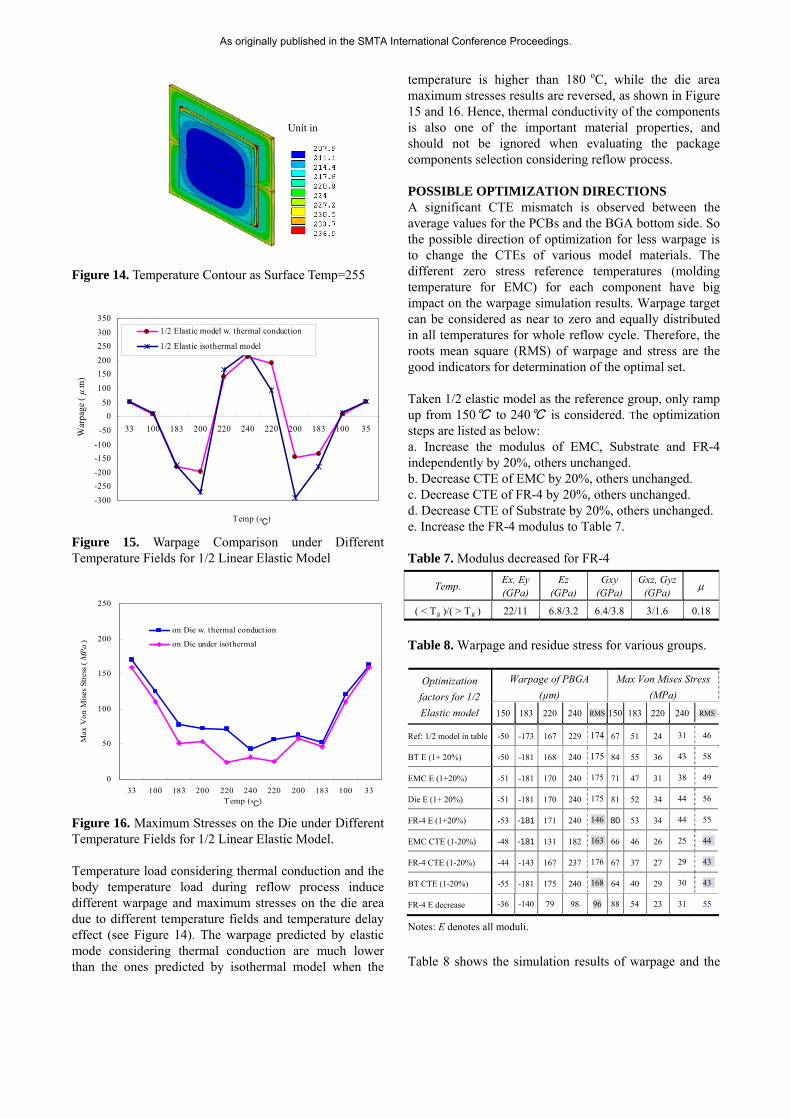
Figure 14. Temperature Contour as Surface Temp=255�
-300
-250
-200
-150
-100
-50
0
50
100
150
200
250
300
350
33 100 183 200 220 240 220 200 183 100 35
Temp (℃)
War
page
( µ
m)
1/2 Elastic model w. thermal conduction
1/2 Elastic isothermal model
Figure 15. Warpage Comparison under Different Temperature Fields for 1/2 Linear Elastic Model
0
50
100
150
200
250
33 100 183 200 220 240 220 200 183 100 33Temp (℃)
Max
Von
Mis
es S
tres
s ( M
Pa
)
on Die w. thermal conduction
on Die under isothermal
Figure 16. Maximum Stresses on the Die under Different Temperature Fields for 1/2 Linear Elastic Model. Temperature load considering thermal conduction and the body temperature load during reflow process induce different warpage and maximum stresses on the die area due to different temperature fields and temperature delay effect (see Figure 14). The warpage predicted by elastic mode considering thermal conduction are much lower than the ones predicted by isothermal model when the
temperature is higher than 180 oC, while the die area maximum stresses results are reversed, as shown in Figure 15 and 16. Hence, thermal conductivity of the components is also one of the important material properties, and should not be ignored when evaluating the package components selection considering reflow process. POSSIBLE OPTIMIZATION DIRECTIONS A significant CTE mismatch is observed between the average values for the PCBs and the BGA bottom side. So the possible direction of optimization for less warpage is to change the CTEs of various model materials. The different zero stress reference temperatures (molding temperature for EMC) for each component have big impact on the warpage simulation results. Warpage target can be considered as near to zero and equally distributed in all temperatures for whole reflow cycle. Therefore, the roots mean square (RMS) of warpage and stress are the good indicators for determination of the optimal set. Taken 1/2 elastic model as the reference group, only ramp up from 150℃ to 240℃ is considered. The optimization steps are listed as below: a. Increase the modulus of EMC, Substrate and FR-4 independently by 20%, others unchanged. b. Decrease CTE of EMC by 20%, others unchanged. c. Decrease CTE of FR-4 by 20%, others unchanged. d. Decrease CTE of Substrate by 20%, others unchanged. e. Increase the FR-4 modulus to Table 7. Table 7. Modulus decreased for FR-4
Temp. Ex, Ey (GPa)
Ez (GPa)
Gxy (GPa)
Gxz, Gyz (GPa)
( < Tg )/( > Tg ) 22/11 6.8/3.2 6.4/3.8 3/1.6 0.18
Table 8. Warpage and residue stress for various groups.
Notes: E denotes all moduli.
Table 8 shows the simulation results of warpage and the
Warpage of PBGA
(µm)
Max Von Mises Stress
(MPa) Optimization
factors for 1/2
Elastic model 150 183 220 240 RMS 150 183 220 240 RMS
Ref: 1/2 model in table -50 -173 167 229 174 67 51 24 31 46
BT E (1+ 20%) -50 -181 168 240 175 84 55 36 43 58
EMC E (1+20%) -51 -181 170 240 175 71 47 31 38 49
Die E (1+ 20%) -51 -181 170 240 175 81 52 34 44 56
FR-4 E (1+20%) -53 -181 171 240 146 80 53 34 44 55
EMC CTE (1-20%) -48 -181 131 182 163 66 46 26 25 44
FR-4 CTE (1-20%) -44 -143 167 237 176 67 37 27 29 43
BT CTE (1-20%) -55 -181 175 240 168 64 40 29 30 43
FR-4 E decrease -36 -140 79 98 96 88 54 23 31 55
Unit in �
As originally published in the SMTA International Conference Proceedings.

maximum von Mesis stress under various combinations of CTE and modulus. Simulation results also show that most of the stress concentration points are around the die, which are caused by the large CTE differences between silicon die and other adjacent components. The CTE mismatch between these components causes warpage and internal stress in the package. In theory, the stress generated is proportional to CTE, temperature and modulus.
Warpages v.s. Modulus or CTE Change
-250
-200
-150
-100
-50
0
50
100
150
200
250
153 183 220 240
Temp (℃)
War
page
( µ
m)
Actual test for PBGA alone Ref: Tref = 180℃ for EMC, BTBT E(1+ 20%) EMC E(1+20%)Die E(1+ 20%) FR-4 E(1+20%)EMC CTE(1-20%) FR-4 CTE(1-20%)BT CTE(1-20%) FR-4 E decrease
Figure 17. Warpages for Different Groups
Max Stress v.s. Modulus or CTE Change
20
40
60
80
100
120
153 183 220 240Temp (℃)
Max
Von
Mis
es S
tres
s (M
Pa)
Ref: Tref = 180℃ for EMC, BT BT E(1+ 20%)EMC E(1+20%) Die E(1+ 20%)FR-4 E(1+20%) EMC CTE(1-20%)FR-4 CTE(1-20%) BT CTE(1-20%)FR-4 E decrease
Figure 18. Residue Stress Distribution around Die for
Different Groups.
Figure 17 and Figure 18 show the warpage trend and the maximum internal stress trend corresponding to temperatures. From the trends, it can clearly be seen that lower CTE and lower modulus are the desirable properties for PBGA in order to reduce both package warpage and stress. Especially low moduli of FR-4 can effectively reduce the warpage at both low and high temperatures, while low FR-4 CTE and low EMC CTE can reduce the warpage at temperature below 200 oC and above 200 oC, respectively. Low CTE of key components can significantly reduce the residue stress around die after cooling down of reflow process, which can effectively
eliminate the cracks and delaminations between silicon die and other adjacent components. Hence, it is important to meet the requirements of coincident CTEs and Moduli in designing a good quality package through selecting reasonable and suitable materials. CONCLUSIONS The accurate prediction for warpage and residue stress of PBGA needs a huge amount of testing, analysis modeling, and fine-tuning. Material properties parameters selection and determination are the most important design step. Specifically, the accurate viscoelastic material behavior needs to be acquired through DMA experiment, which requires certain expertise in polymer material and the complicated curve-fitting techniques. Necessary measurements on either warpage or stress are much needed to validate the effectiveness of the FEA model. Viscoelastic calculation considering thermal conduction using the 1/2 solid element model is the most appropriate method for predicting both the warpage and the stress of PBGA during SMT reflow process. However, due to large computing time and convergence concerns, a strip model can also be used to predict accurate warpage profile. The stress prediction using strip viscoelastic model in this paper still needs to be validated through consideration of thermal conduction in future work. The warpage and solder joint defects optimization results show that the CTE mismatch between the components causes warpage and internal stress in the package. Low CTE of key components can significantly reduce the residue stress around the die area, which can effectively eliminate cracks and delaminations between silicon die and adjacent components. Hence, it is meaningful to optimize the coincident CTEs and Moduli through materials’ selection for a good quality package design.
FUTURE WORK With the assemblies cool down to room temperature, bending and stress are generated due to the CTE mismatch. Reflow process simulation with different temperature profiles will help to optimize the solder quality and eliminate the residue stress concentration after reflow process. Heating temperature ramp rate and cooling rate can be taken as further optimization factors. Fatigue life cycles prediction for solder joints is another good subject for evaluation of the lead-free solder joints reliability. The thermo mechanical simulation for package dimensional design and material selection is very useful for the miniaturization development and performance improvement in microelectronics assembly. Due to the viscoelastic properties of epoxy-based materials, it is necessary to understand the effect of curing temperature, curing time and post curing process on the molding compound material behavior to improve solder joints quality of PCB assembly.
As originally published in the SMTA International Conference Proceedings.

ACKNOWLEDGEMENTS The authors would like to express their sincere gratitude to Kaifa top management, Mr. LM Phua and Mr. Chon Vo, for providing great support and understanding for this work. The authors are also willing to acknowledge the supports from QA team, Operation team of Kaifa, in particular from Mr. Bibo Tu, Mr. Zhiming Mo and Mr. Bin Deng. In addition, thanks to Prof. Dayong Gui and Dr. Hongchao Sheng from Shenzhen University for DMA testing support. REFERENCES [1] D. Lu, C.P. Wong, Materials for Advanced Packaging, Springer Science, 2009, pp. 339. [2] W. van Driel, G. Zhang and X. Fan. Thermo-Mechanics of Integrated Circuits and Packages, Solid Mechanics and Its Applications, Mechanics of Microelectronics, Springer Netherlands.2006 pp. 169. [3] S.Y. Zhang, B.L. Zheng, Numerical Simulation for Electronic Package Warpage due to Geometrical Dimension, Chinese Quarterly of Mechanics, Vol. 26, No. 3, 2005, pp.506. (in Chinese) [4] K. Miyake, T. Yoshida, H.G. Baik and S.W. Park, Viscoelastic Warpage Analysis of Surface Mount Package, ASME Transactions Journal of Electronic Packaging, ASME, Jun 2001, Vol. 123, pp.101. [5] Q.T. Yang, W.P. Luo, P. Xu, Y.T. Wei and Q.G. Gang, Viscoelastic Theory and Applications, Science Press. 2004, pp. 13. (in Chinese) [6] L.J. Ernst, C.van’t Hof, D.G. Yang, M.S. Kiasat, “Determination of Visco-Elastic Properties during the Curing Process of Underfill Materials”, Electronic Components and Technology Conference, 2000, pp. 1070. [7] D.G. Yang, G.Q. Zhang, L.J. Ernst. Combined Experimental and Numerical Investigation on Flip Chip Solder Fatigue with Cure-dependent Underfill Properties. 2001 Electronic Components and Technology Conference. [8] Z.G. Wang, Modeling the Viscoelastic Properties of Epoxy Molding Compound during Post Mold Cure in IC Packaging, M.S. Thesis, National Chenggong University, 2006, pp.30. [9] ANSYS Theory Reference. [10] S. Banerji, P.M. Raj. Warpage-Induced Lithographic Limitations of FR-4 and the Need for Novel Board Materials for Future Microvia and Global Interconnect Needs. IEEE Transactions on Advanced Packaging, 2005 [11] D.K. Shangguan, Lead-free Solder Interconnection Reliability, ASM International, 2008, pp.224 [12] J. Zhao, The Finite Element Modeling and Simulation for Thermomechanical Analysis of PCBA, M.S. Thesis,Tianjin University, 2006 (in Chinese) [13] R. Dudek. Characterization and Modelling of Solder Joint Reliability, Solid Mechanics and Its
Applications, Mechanics of Microelectronics, Springer Netherlands. 2006, pp377. [14] J.Z. Jiang, F.L. Sun, L.F. Wang and Y. Liu, Numerical Simulation of Stress-strain and Life Prediction for Lead-free Solder Joints of PBGA Package, Journal of Herbin Univ. Science & Technology, 2007, pp156-159 (in Chinese) [15] Y. Qi, R. Lam, H.R. Ghorbani, P. Snugovsky, J.K. Spelt, Temperature profile effects in accelerated thermal cycling of SnPb and Pb-free solder joints, Microelectronics Reliability, 46, 2006, pp.574 [16] Z.Y. Liu, C.Y. He, H.F. Ran, L. Wang, H.X. Wang and F. Lu, Influence of PBGA Thermo Warpage on Soldering Joints' Quality & Reliability, SMTA China, Shenzhen, 2009. (in Chinese)
As originally published in the SMTA International Conference Proceedings.