system architecture and circuit design for micro and
TRANSCRIPT

HAL Id: tel-00658843https://tel.archives-ouvertes.fr/tel-00658843v2
Submitted on 2 Oct 2013
HAL is a multi-disciplinary open accessarchive for the deposit and dissemination of sci-entific research documents, whether they are pub-lished or not. The documents may come fromteaching and research institutions in France orabroad, or from public or private research centers.
L’archive ouverte pluridisciplinaire HAL, estdestinée au dépôt et à la diffusion de documentsscientifiques de niveau recherche, publiés ou non,émanant des établissements d’enseignement et derecherche français ou étrangers, des laboratoirespublics ou privés.
System architecture and circuit design for micro andnanoresonators-based mass sensing arrays
Grégory Arndt
To cite this version:Grégory Arndt. System architecture and circuit design for micro and nanoresonators-based masssensing arrays. Other [cond-mat.other]. Université Paris Sud - Paris XI, 2011. English. NNT :2011PA112358. tel-00658843v2

!
!
!
N° d’ordre!"!#$%%&#'&()!!
!
!"#$%"&'('$$
)!*+,-.,%/0$!1/),+)$$!
Ecole Doctorale « Sciences et Technologies de l’Information des$%232456678(49:(58'$&:$;&'$)<':=6&'$>!
!!!
!"#$#
!
?@&A5@<$-BC#%$!!!!"#$%&'()!!"*+(&,!-.'/0(&'(#.&!-12!'0.'#0(!2&+031!45.!,0'.5!-12!1-15.&+51-(5.+6$-+&2!,-++!+&1+013!
-..-*+!!!!!7&4&12&2!(/&!89!7&'&,$&.!9:88!;0(/!(/&!45<<5;013!%#.*!,&,$&.+)!!!!#@$D73(&8$-@49658&! =>?6@>ABC!D01-(&'! "#E&.F0+5.!
#@$C7@(9$E9@8(53! G10F&.+0(-(!?#(515,-!2&!H-.'&<51-! I-EE5.(&#.!
#@$-39(8$E5''&F5&7G! G10F&.+0(J!K-.0+!88C!B>L! K.&+02&1(!54!(/&!%#.*!
#@$*@(4$+53(8&:! =>?6@>ABC!D01-(&'! "#E&.F0+5.!
H6&$B5'&IH9@(&$+9J&339! Direction Générale de l’Armement! >M-,01&.!
#@$!"(3(J$K&8A! =-+&!N&+(&.1!G10F&.+0(*C!>=">!L-'#<(*!! I-EE5.(&#.!
#@$D2@L6&$D7(339@;! "#EJ<&'C!"">! "#E&.F0+5.!
#@$!9'493$C57&:! =OI"C!@BIDD! >M-,01&.!
!
Université Paris Sud


Acknowledgments
I gratefully acknowledge the guidance provided by my director, Prof. Jérôme Juil-lard, for my entire PhD project. I always appreciated his advice and admired howavailable he always was even when our backgrounds and our research interests di-verged. I am also very grateful for his help and guidance during the difficult taskof scientific writing. I extend my thanks to Dr. Eric Colinet, particularly for thesupport and the supervision during my use of the many different devices employedin the different projects. I also thank him for choosing my PhD subject, and histolerance to my attitude which can sometimes be quite stubborn. I am particularlygrateful for his vision which provided depth and substance to my PhD. Dr. JulienArcamone and Gérard Billot guided and taught me about the fabrication processand analog design and I will always be grateful for the skills they gave me.
Towards the end of my PhD, I particularly appreciated the help provided by JulienPhilippe during his internship. He has characterized many co-integrated devices andprovided invaluable expertise. I also appreciated his positive attitude and thoroughlyenjoyed working with him. I also acquired first-hand experience of managementthrough our interaction. I wish him all the best in his ongoing PhD studies. I amalso grateful for the time and the interesting technical discussions I had with PaulIvaldi, Dr. Cécilia Dupré, Dr. Laurent Duraffourg, Dr. Patrick Villard, Dr. ThomasErnst, Dr. Sébastien Hentz, Patrick Audebert, Sylvain Dumas, Dr. GuillaumeJourdan and many others. I have also appreciate the enjoyable and profitable timespent in Leti due largely to the input and friendship of Olivier Martin, MatthieuDubois, Eric Sage, Dr. Marc Belleville, and Pierre Vincent.
I thank Prof. Nuria Barniol and Dr. Philip Feng for their time and interest towardsmy PhD manuscript and defense. I appreciated their constructive remarks andadvice. I also thank Prof. Pascal Nouet and Prof. Alain Bosseboeuf for comingto my PhD defense and their interesting questions. I was particularly grateful thatProf. Alain Bosseboeuf accepted to be the president of the jury.
Finally, my thoughts go to my family (particularly my parents) and friends whoencouraged me during my studies. I am sure I could not have finished my PhDwithout their support.
3


Contents
Abstract 1
General introduction 3
1 Harmonic detection of resonance 71.1 MEMS resonator model . . . . . . . . . . . . . . . . . . . . . . . . . 7
1.1.1 Mechanical resonance . . . . . . . . . . . . . . . . . . . . . . . 71.1.2 Feed-through transmission . . . . . . . . . . . . . . . . . . . . 91.1.3 MEMS noise sources . . . . . . . . . . . . . . . . . . . . . . . 12
1.2 Open loop resonant frequency tracking . . . . . . . . . . . . . . . . . 131.2.1 Frequency sweep . . . . . . . . . . . . . . . . . . . . . . . . . 161.2.2 Amplitude or phase-shift variation measurement . . . . . . . . 16
1.3 Closed loop resonant frequency tracking . . . . . . . . . . . . . . . . 191.3.1 Self-oscillating loop . . . . . . . . . . . . . . . . . . . . . . . . 201.3.2 Frequency-locked loop . . . . . . . . . . . . . . . . . . . . . . 27
1.4 Oscillating frequency measurement . . . . . . . . . . . . . . . . . . . 321.4.1 Period-counting . . . . . . . . . . . . . . . . . . . . . . . . . . 331.4.2 Delay-based measurement . . . . . . . . . . . . . . . . . . . . 331.4.3 PLL-based measurement . . . . . . . . . . . . . . . . . . . . . 35
1.5 Conclusion . . . . . . . . . . . . . . . . . . . . . . . . . . . . . . . . . 35
2 Various MEMS resonators topologies and their readout electronics 392.1 The mechanical resonator . . . . . . . . . . . . . . . . . . . . . . . . 392.2 MEMS topologies to make portable, low-power, mass sensors . . . . . 41
2.2.1 Clamped-clamped beam with capacitive detection . . . . . . . 432.2.2 Clamped-clamped beam with piezoresistive detection . . . . . 462.2.3 Crossbeam with piezoresistive detection . . . . . . . . . . . . . 482.2.4 Piezoelectric cantilever . . . . . . . . . . . . . . . . . . . . . . 492.2.5 Conclusion . . . . . . . . . . . . . . . . . . . . . . . . . . . . . 52
2.3 Interconnections between the MEMS resonator and the readout elec-tronics . . . . . . . . . . . . . . . . . . . . . . . . . . . . . . . . . . . 532.3.1 Basic model of the MEMS-to-electronics connection losses . . 542.3.2 Interconnection schemes . . . . . . . . . . . . . . . . . . . . . 572.3.3 Heterodyne architectures . . . . . . . . . . . . . . . . . . . . . 642.3.4 Conclusion on MEMS-to-electronics interconnections . . . . . 65
i

Contents Contents
2.4 MEMS resonators mass resolution comparison . . . . . . . . . . . . . 662.4.1 Model presentation . . . . . . . . . . . . . . . . . . . . . . . . 662.4.2 Results and discussions . . . . . . . . . . . . . . . . . . . . . . 69
2.5 Collectively addressed MEMS arrays . . . . . . . . . . . . . . . . . . 732.5.1 Amplification gain . . . . . . . . . . . . . . . . . . . . . . . . 732.5.2 Signal-to-noise ratio optimization . . . . . . . . . . . . . . . . 762.5.3 Minimal number of MEMS resonators to reach the best array
performance . . . . . . . . . . . . . . . . . . . . . . . . . . . . 772.5.4 Results, discussions . . . . . . . . . . . . . . . . . . . . . . . . 782.5.5 Conclusion of collectively-addressed MEMS arrays . . . . . . . 81
2.6 Conclusion . . . . . . . . . . . . . . . . . . . . . . . . . . . . . . . . . 81
3 Practical realizations 833.1 Self-oscillating loops using discrete electronics . . . . . . . . . . . . . 83
3.1.1 Self-oscillating loop with a piezoelectric micro-cantilever . . . 833.1.2 Self-oscillating loop with a piezoresistive crossbeam . . . . . . 923.1.3 Conclusion of self-oscillating loops using discrete electronics . 100
3.2 Integrated circuit for multiple crossbeams . . . . . . . . . . . . . . . . 1003.2.1 Objective of the integrated circuit . . . . . . . . . . . . . . . . 1003.2.2 Global architecture . . . . . . . . . . . . . . . . . . . . . . . . 1023.2.3 General topology of the proposed oscillator . . . . . . . . . . . 1033.2.4 Analog circuit design . . . . . . . . . . . . . . . . . . . . . . . 1053.2.5 Overall simulations and layout . . . . . . . . . . . . . . . . . . 108
3.3 MEMS/CMOS co-integration . . . . . . . . . . . . . . . . . . . . . . 1093.3.1 Context and objectives . . . . . . . . . . . . . . . . . . . . . . 1093.3.2 Theoretical design of a co-integrated MEMS Pierce oscillators 1113.3.3 2D co-integration of resonators with capacitive detection and
a 0.35 µm CMOS circuit . . . . . . . . . . . . . . . . . . . . 1223.3.4 2D co-integration of resonators with piezoresistive detection
and a 0.3 µm CMOS circuit . . . . . . . . . . . . . . . . . . . 1283.3.5 3D co-integration of resonators with piezoresistive detection
and a 30 nm CMOS circuit . . . . . . . . . . . . . . . . . . . 1353.3.6 Conclusion of MEMS/CMOS co-integration . . . . . . . . . . 139
3.4 Conclusion . . . . . . . . . . . . . . . . . . . . . . . . . . . . . . . . . 141
General conclusion 143
Nomenclature 147
Bibliography 157
Personal publications 167
Appendix A: determination of the dynamic range in self-oscillating loops 169
ii

Contents Contents
Appendix B: multi-mode frequency response of a beam 173
Appendix C: comparison of commercial electronic amplifiers 179
iii


Abstract
This manuscript focuses on micro or nanomechanical resonators and their surround-ing readout electronics environment. Mechanical components are employed to sensemasses in the attogram range (10≠18 g) or extremely low gas concentrations. Thestudy focuses particularly on circuit architectures and on resonators that can beimplemented in arrays.
In the first chapter, several architectures for tracking the resonance frequency of themechanical structure (used to measure a mass) are compared. The two major strate-gies are frequency locked-loops and self-oscillating loops. The former is robust andversatile but is area-demanding and difficult to implement into a compact integratedcircuit. Self-oscillating loops are compact but are sensitive to parasitic signals andnonlinearity. This architecture was chosen as the focus of the PhD project becauseof its compactness, which is necessary for the employment of arrays of sensors.
In the second chapter, the electromechanical response of a sensor composed of a me-chanical resonator and an appropriate electronics is assessed. Four resonators werechosen for mass spectrometry on the basis of their power consumption and integra-bility. Their transduction mechanisms are described and an electrical model of eachcomponent is developed. The study then focuses on the integration scheme of theresonators with their readout electronics. The technological process, developmentcost and electrical model of stand-alone, 2D- and 3D-integration schemes are de-scribed. Finally, the phase-noise improvement of integrating mechanical resonatorsin collectively addressed arrays is assessed.
In the third chapter, two self-oscillating loops using either a piezoelectric or a cross-beam resonator are described. The former demonstrates that is it possible to builda self-oscillating loop even when the resonator has a large V-shaped feed-through.In the second oscillator an excellent mass resolution is measured, comparable tothat obtained with frequency-locked loops. The oscillator time response is below100 µs, a level that cannot be reached with other architectures. The design of apromising integrated circuit in which four resonators self-oscillate simultaneously isdescribed. Thanks to its compactness (7 ◊ 7 mm2), it is also possible to implementthe circuits in arrays so as to operate 12 or more sensors. Finally, the integration onthe same wafer of the resonator and its sustaining electronics is explored. We firstfocus on two projects whereby the electronics are 2D-integrated with a resonatorusing either capacitive or piezoresistive detection, and then on a third project us-ing a 3D-integration scheme in which the circuitry is first fabricated and then theresonator is constructed on top on it.
1


General introduction
The omnipresence of CMOS technology in our everyday life demonstrates the successof microelectronics and the quest to make electronic circuits ever more compact.A key component of all circuits is the transistor which transforms an electricalsignal to create logic functions (AND, NO, OR ...), memories, amplifiers, or morecomplex digital or analog electronic functions. As the dimensions of transistorsdiminish, they become faster and cheaper. Using the extraordinary capacity ofthe engineered fabrication process that is inherent to CMOS technology, scientistshave also developed mechanical structures that interact physically at the micro- ornano-scale. Such components, called MicroElectroMechanical Systems (MEMS) areused as sensors that transform a physical stimulus into an electrical response, or asactuators where an electrical stimulus is converted into a mechanical or a physicalresponse. Among the most sought after MEMS components are resonators thatcan be used to determine the stiffness or mass of the structure from its mechanicalresonance.
As with transistors, the size of MEMS components is shrinking: progressing fromMicroElectronicMechanical Systems to NanoElectroMechanical Systems (NEMS).For the sake of simplicity, the word “MEMS” is used throughout the rest of thethesis to designate indifferently MEMS or NEMS. Reducing the dimensions of themechanical device has several benefits. Among them, the fabrication process isgetting compatible with a CMOS process because the release dimensions are low.
In fact, the term NEMS refers to mechanical components that present at leasttwo submicron dimensions. Scaling down the dimensions of the mechanical devicepresents several benefits: compact sensors can be fabricated, the sensing capabilitycan be enhanced and the quality factor of the mechanical structure in air is com-monly improved [Li 2007]. Indeed, the mechanical displacement of the nanoscaleproof mass can be smaller than the mean free path of air reducing the effects of theviscous damping of air. Smaller components interact better with the nanoscale worldand can sense unprecedented physical and biological variations. A notable challengeis to measure directly the mass of a single molecule [Knobel 2008, Naik 2009]. Inpractice, the limit of mass detection (or mass resolution) is commonly used by re-searchers to assess the performance of the device.
MEMS components have many other applications such as the measurement of force[Mamin 2001, Kobayashi 2011] (as in living cells), thermal fluctuation [Paul 2006],or biochemical reaction [Campbell 2006, Burg 2007]. In particular, NEMS compo-nents should eventually be used in mass spectrometry [Chiu 2008, Naik 2009] or gas
3

General introduction
analysis [Boisen 2000, Hagleitner 2001, Lang 1998, Tang 2002]. With their fast re-sponse and their excellent mass resolution, the nano-devices can potentially achievesimilar resolution to conventional mass spectrometers or gas chromatographs butat a lower cost, an enhanced compactness, and with a faster time response becausethey work at a higher frequency.
Mass spectrometry is used in a large range of applications such as medicine, bi-ology, geochemistry and many others. In a conventional mass spectrometer thesample is first ionized, a mass analyzer is used to determine the mass-to-chargeratio of the ionized particles and finally a detector counts the number of ions[Aebersold 2003, Russell 1997, Domon 2006]. Conventional mass spectrometry cantherefore be applied only to ionizable particles. Their inherent limits of resolutionand response time have hindered progress of biology or other sciences [Naik 2009].Critical parameters of mass spectrometers are their mass accuracy, resolving power(the ratio between the mass of the detected molecule and the minimum detectablemass) and dynamic range (ratio between the maximum detectable mass and theminimum detectable mass) [Domon 2006]. To obtain high-quality data commonlyrequires very long measurement times that can last up to 24 hours for certain sam-ples. The limited performance of even the best equipment makes it impossible toreach what might be called the holy grail of biology: the measurement of the massof every molecule of a single cell.
The Roukes group at the California institute of technology [Naik 2009] proposed touse MEMS components as an alternative to conventional mass spectrometers. Thelatest nano-components in the literature have mass resolutions sufficient to measuresingle molecules in a few seconds or less [Jensen 2008, Yang 2006]. A MEMS-basedmass spectrometer would have several advantages: it would be sensitive to non-ionized molecules, would have a mass resolution independent of the mass of themolecule and would be relatively cheap thanks to microfabrication. To constructa MEMS-based mass spectrometer, several challenges must be resolved, notablythe design and fabrication of robust MEMS components, the development of anarchitecture compatible with large arrays of MEMS devices, and the implementationof arrays of sensors with low coupling effects within the arrays.
The three years of research summarized up in this manuscript focus on the archi-tecture analysis of a sensor constructed from a passive MEMS component and itsassociated readout electronics. The topologies of several relevant MEMS devices formass spectrometry applications are presented and compared. The interface betweenthe MEMS component and the first electronic amplifier is described in detail andits influence on the performance of the sensor is evaluated. Finally, the design andcharacterization of several MEMS-based sensors relevant for mass spectrometers arepresented.
The manuscript is organized as follows. In the first chapter, a simple generic modelof a MEMS resonator is introduced. From the description of the nano-device, differ-ent architectures that measure the resonance frequency of the nano-component are
4

General introduction
presented. They can be divided into two categories: open and closed loop measure-ments. It is shown that although the first is simple to implement, it has a limiteddynamic range and is expensive to design and fabricate. Open-loop architectureshave therefore been rejected for mass spectrometry applications. In closed-loop ar-chitectures, the sensor (composed of the mechanical resonator and its sustainingelectronics) has a larger dynamic range and in most cases is limited by the nano-component and not by the architecture itself. Two major types of closed loops arepresented in the literature: self-oscillating loops and frequency-locked loops. Thelatter, comprising a phase-comparator, a low-pass filter and a Voltage-ControledOscillator (VCO), is the most popular in the MEMS domain because it is robustand has low distortion. Most of all, the frequency range of the loop can be adjustedto prevent any undesired parasitic oscillations. Self-oscillating loops, comprisingamplifiers and filters, are much cheaper to implement and can be very compact. Inthis architecture, the electronics compensates the attenuation and the phase-shiftintroduced by the nano-device at the resonance frequency so that the loop oscillatesat this frequency. This approach is adopted in the rest of this work because thecompactness of architecture is crucial when designing arrays of nano-resonators (asin mass spectrometers or gas analyzers). In the last section of chapter 1, variousfrequency measurement techniques necessary for self-oscillating loops are presentedand compared.
The second chapter is dedicated to the theoretical assessment of different MEMSresonators. First, the electromechanical behavior of different resonator topologiesis described. Four nano-resonators that meet the requirements of mass spectrome-try were chosen on the basis of the following criteria: they should be individuallyaddressable and have a low power consumption (to allow an implementation of thecomponents in arrays). They use either electrostatic or piezoelectric actuation, andcapacitive, piezoresistive or piezoelectric detection. In the second section, differentMEMS and electronics integration schemes are presented. The process flow of eachscheme is described and compared. A simple electrical model assesses the connec-tion losses and the feed-through introduced by each integration scheme. Differentactuation and layout techniques for enhancing the electrical response of the res-onators are then described. Using the electromechanical behavior of the resonators,the integration schemes, and the results presented in the first chapter, it is thenpossible to determine the theoretical mass resolution of each nano-component andthus to objectively compare each resonator. The comparison is based on the 65nm-CMOS process flow of STMicroelectronics, which is compatible with the fabricationof nano-resonators and high frequency analog circuits. The last section is dedicatedto the theoretical assessment of collectively-addressed parallel arrays of MEMS res-onators. It is shown that an intrinsic electrical limitation remains when the size ofthe array increases.
In the third chapter, the different designs and experimental characterizations re-alized during the PhD project are presented. The initial focus is on stand-aloneself-oscillating loops in which the sustaining electronics are built using commercial
5

General introduction
amplifiers. The first self-oscillating loop uses a piezoelectric cantilever that intro-duces large feed-through. The main objective is to prevent the loop from oscillatingat undesired frequencies due to the the feed-through. The frequency resolution of theloop is then compared to that of a frequency-locked loop. The second self-oscillatingloop is based on a crossbeam resonator that oscillates at 20 MHz. The objective hereis to implement a differential actuation that would compensate for the feed-throughintroduced by the coupling between each cable and within the silicon chip. Thetime response of the loop is then measured and shows to have state-of-the-art massresolution. The second section presents the design of an ASIC for stand-alone cross-beams. The design comprises four self-oscillating loops (including four frequencycounters) making it possible to operate four different crossbeams in parallel. Eachself-oscillating loop is controlled and can be deactivated using an SPI interface withthe computer. The coupling in the ASIC and in the MEMS chip can thus be eval-uated. The final section presents the design and preliminary characterization ofco-integrated MEMS-CMOS devices. In the first two designs, the nano-componentis fabricated on the same wafer and next to the electronic circuit (2D monolithicintegration). In the third design, the resonator and circuit are co-integrated in a 3Dapproach: the nano-device is fabricated on top of the transistors.
6

1 Harmonic detection of resonance
This chapter describes general architectures of electronic readout for MEMS res-onators. It first presents a system architecture oriented description of the MEMScomponent and what limits its performance. It also describes common open- andclosed-loop architectures for measuring the resonance frequency of the MEMS de-vice. The limitations and specifications of the electronics are determined and com-pared. This chapter therefore provides a general description of the architecture ofthe MEMS component and its electronic readout and provides guidelines to designoptimal MEMS resonators matching with their readout electronics.
In the manuscript, the following notation convention is used. The complex amplitudeof a signal is written in italic, while its temporal expression is written using the“sans serif” font. For example, the complex amplitude voltage at the input of theelectronics is referred to Velec (f), while its expression in the temporal domain iswritten Velec (t). The DC component of the signal is referred with the subscript“-DC”: Velec≠DC in the example. The small signal component of Velec (t) is referredto velec (t). Obviously, the amplitude of velec (t) is velec (f) in the frequency domain.Generally, the power spectral density of the noise expressed at a node is referredto Sxx (f) where xx describes the noise source. For example, the electronic noiseexpressed at velec is referred to Selec (f) (the node where the noise is expressed isgiven in the text when needed).
1.1 MEMS resonator model
The aim of this section is to establish a model of the MEMS component that is com-mon to all resonant MEMS topologies presented in the manuscript, and that makesit possible to introduce the objectives and the constraints of harmonic detection ofresonance. It provides the expressions of MEMS response to an input signal and ofthe MEMS generated noise. The physical explanations of the MEMS resonator willbe further described in chapter 2.
1.1.1 Mechanical resonance
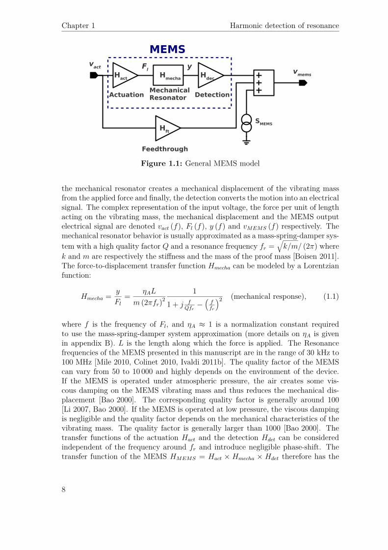
MEMS resonators are composed of a vibrating body acting as a mechanical res-onator, means of actuation and means of detection (fig. 1.1). They can be decom-posed into three main blocks: the actuation converts the input voltage into a force,
7
Chapter 1 Harmonic detection of resonance
!"#$%&'#%()"*+&%,+-
.%#,
./"#$%
0#,1%,'+& 2","#,'+&
!3!4
!"#"$
!%&'
.5"#
.6,
4!3!4
7""5,$-+18$
()
*
Figure 1.1: General MEMS model
the mechanical resonator creates a mechanical displacement of the vibrating massfrom the applied force and finally, the detection converts the motion into an electricalsignal. The complex representation of the input voltage, the force per unit of lengthacting on the vibrating mass, the mechanical displacement and the MEMS outputelectrical signal are denoted vact (f), Fl (f), y (f) and vMEMS (f) respectively. Themechanical resonator behavior is usually approximated as a mass-spring-damper sys-
tem with a high quality factor Q and a resonance frequency fr =Ò
k/m/ (2π) where
k and m are respectively the stiffness and the mass of the proof mass [Boisen 2011].The force-to-displacement transfer function Hmecha can be modeled by a Lorentzianfunction:
Hmecha =y
Fl
=ηAL
m (2πfr)2
1
1 + j fQfr
≠1
ffr
22 (mechanical response), (1.1)
where f is the frequency of Fl, and ηA ¥ 1 is a normalization constant requiredto use the mass-spring-damper system approximation (more details on ηA is givenin appendix B). L is the length along which the force is applied. The Resonancefrequencies of the MEMS presented in this manuscript are in the range of 30 kHz to100 MHz [Mile 2010, Colinet 2010, Ivaldi 2011b]. The quality factor of the MEMScan vary from 50 to 10 000 and highly depends on the environment of the device.If the MEMS is operated under atmospheric pressure, the air creates some vis-cous damping on the MEMS vibrating mass and thus reduces the mechanical dis-placement [Bao 2000]. The corresponding quality factor is generally around 100[Li 2007, Bao 2000]. If the MEMS is operated at low pressure, the viscous dampingis negligible and the quality factor depends on the mechanical characteristics of thevibrating mass. The quality factor is generally larger than 1000 [Bao 2000]. Thetransfer functions of the actuation Hact and the detection Hdet can be consideredindependent of the frequency around fr and introduce negligible phase-shift. Thetransfer function of the MEMS HMEMS = Hact ◊ Hmecha ◊ Hdet therefore has the
8

1.1 MEMS resonator model
following expression:
HMEMS =vMEMS
vact
=gMEMS/Q
1 + j fQfr
≠1
ffr
22 (MEMS response), (1.2)
where gMEMS = ηAQL
m(2πfr)2 |HactHdet| is the modulus of HMEMS at f = fr. Note that
the argument of HMEMS at fr is arg (HMEMS) = ≠90°. Figure 1.2 presents a typicalresonance response of a MEMS corresponding to equation (1.2). The MEMS has a
bandpass filter behavior. It can be determined that at f = fr
11 ± 1
2Q
2, the MEMS
gain is reduced by 3 dB (or divided byÔ
2). Similarly to amplifiers, it is said thatthe MEMS has a bandwidth of fr/Q.
Frequency
Reso
nato
r g
ain
gMEMS√
2
gMEMS
fr(1 – 1
2Q) fr fr(1 +
1
2Q)
(a)
0
−90
−180
−45
−135
Frequency
Reso
nato
r p
hase−
sh
ift
[°]
fr
(b)
Figure 1.2: Theoretical Bode diagram of a MEMS resonator.
If the vibration amplitude is large, the resonator response becomes nonlinear, duefor example due to mechanical stiffening effects, and the performance of the deviceas a sensing element can be jeopardized. All studies in this manuscript are thereforelimited to resonators whose responses are considered linear. The critical actuationvoltage, critical actuation force and critical mechanical displacement below whichthe behavior of the system can be considered as linear are respectively called vact≠c,Fl≠c and yc. Much work has been accomplished to study the nonlinear regimeof micromechanical resonators [Juillard 2009, Kacem 2008, Mestrom 2009] but thistopic is not treated in this manuscript.
1.1.2 Feed-through transmission
In addition to the previous electromechanical description of the resonator, it can benecessary to introduce input-to-output parasitic elements in the MEMS componentmodel. They introduce so-called feed-through transmission that adds to the MEMSoutput signal a signal varying with vact. Feed-through transmission may come from
9

Chapter 1 Harmonic detection of resonance
Figure 1.3: Theoretical effect of a constant feed-through on the gain (left) and theargument (right) of the MEMS transfer function
intrinsic capacitance in the MEMS, material losses (e.g. dielectric losses) or para-sitic coupling [Lee 2009b, Arcamone 2010]. These effects can be modeled by addingto HMEMS another transfer function Hft(f) that is independent of the mechani-cal resonator. The MEMS transfer function including feed-through transmissionHMEMSft(f) becomes:
HMEMSft(f) =gMEMS/Q
1 + j fQfr
≠1
ffr
22 + Hft(f). (1.3)
To simplify the notations, HMEMSft will be denoted HMEMS in the rest of themanuscript. Hft is usually modeled as a frequency independent transfer functionwith a real gain. Similarly to [Lee 2009b] figure 1.3 (left) shows the theoretical effectof a constant feed-through on the MEMS modulus response. Figure 1.3 (right) showsthe theoretical effect of the feed-through on the phase-shift response induced by theMEMS. In figure 1.3, the feed-through is modeled by a frequency independent realgain. If the feed-through gain has a value close to the MEMS gain at the resonance,then the detection of the resonance frequency may become challenging.
Sometimes a more complex description of Hft is required (see chapter 3). It canoccur when the feed-through is locally compensated with adjustable componentssuch as a variable capacitance and/or a variable resistance. The feed-through islocally minimized around fr but can be significant out of the band of interest.Indeed, the MEMS intrinsic feedthrough can vary with the frequency and thus thefeedthrough compensation is largely increased out of the resonance frequency. Amodel of V-shape feed-through can be expressed as the following:
Hft (f) Ã fpftr ≠ fpft
fpftr
(V-shape feed-through), (1.4)
where pft is a parameters that models the frequency dependence of the V-shape feed-through. Figure 1.4 depicts a V-shape feed-through. A more detailed description of
10

1.1 MEMS resonator model
10−1
100
101
10−1
100
Normalized frequency
Gain
Figure 1.4: Illustration of a V-shape feed-through.
10−2
100
102
102
103
104
Hft /g
MEMS ratio
Absolu
te s
lope
of
ΨM
EM
S×f r [
°]
Q=100
Slope at ψ
MEMS=−90°
Slope at fr
Maximumslope
Figure 1.5: Evolution of---∂ψMEMS
∂f
--- versusthe feed-through transmission.
the V-shape model is given in chapter 3.
It will be shown that a key feature in MEMS resonators is the absolute value of thephase-slope,
---∂ψMEMS
∂f
--- because the resolution of the sensors improves when---∂ψMEMS
∂f
---
increases. When there is no feed-through, the maximum of---∂ψMEMS
∂f
--- is obtained for
f = fr and its value is 2Q/fr. However, the feed-through can reduce this slope andthus the resolution of the sensor. Three scenarios are described in this subsection:the slope at fr, the maximum absolute slope and the slope at the frequency whereψMEMS = ≠90°. It is assumed in this subsection that Hft is real, positive andconstant around fr. From (1.3), we have:
ψMEMS (f) = arg
SWWU
gMEMSQ
11 ≠ f2
f2r
2≠ j f
Qfr
gMEMSQ + Hft
511 ≠ f2
f2r
22+
1f
Qfr
226
11 ≠ f2
f2r
22+
1f
Qfr
22
TXXV
(1.5)
= ≠π
2≠ arctan
SUQ
3fr
f≠ f
fr
4+
Hft
gMEMS
SUfr
fQ2
A1 ≠ f2
f2r
B2
+
3f
fr
4TV
TV .
The slope at fr is thus:
∂ψMEMS
∂f(fr) =
1
fr
Hft
gMEMS≠ 2Q
1 +1
Hft
gMEMS
22 ¥ ≠ 2Q/fr
1 +1
Hft
gMEMS
22 . (1.6)
It is clear that---∂ψMEMS
∂f
--- (fr) reduces with feed-through.
In the other scenarios, the calculations are more complex and thus are not presentedin the manuscript. Figure 1.5 depicts the evolution of the slope versus the feed-through. One can see that the slope is optimum if the feed-through is ten times ormore smaller than gMEMS. The slope at ψMEMS = ≠90° then decreases quickly. It
11

Chapter 1 Harmonic detection of resonance
is also shown on the figure that it can be interesting to actuate the MEMS resonatorat a frequency slightly different from fr in order to improve the slope.
1.1.3 MEMS noise sources
The readers interested in thebasics of noise analysis should consult [Rubiola 2008].The definitions and the notations related to noise processes are based on the samebook. The random processes in the manuscript are considered as stationary1 andergodic2. A noise process is commonly described by its power spectral density (PSD)defined as:
Sx (f) © F [Γτ (x)] ©ˆ
R
Γτ (x) e≠2πjfτ dτ (power spectral density)
©ˆ
R
Eτ x (t) x (t + τ) e≠2πjfτ dτ, (1.7)
where F [x (t)] ©´
Rx (t) e≠2πjftdt is the Fourier transform of x (t), E is the statis-
tical expectation and Γτ (x) © Eτ x (t) x (t + τ) is the auto-correlation function ofx (t). The most common noise representation is white noise where the power spectraldensity is independent of the frequency. In opposition, other noises are referred tocolored noises. For example, pink or flicker noise has a PSD inversely proportionalto the frequency.
An inherent noise in the resonator is thermomechanical noise that can be modeled asa white noise acting at the input of the mechanical resonator block [Cleland 2002].Other noise sources can be considered such as Johnson noise or from more complexphenomena as invariant fluctuations [Cleland 2002]. The different noises generatedby the MEMS can be modeled as a noise source at the output of the MEMS thatis composed of white noise, frequency-dependent noise, and more complex behavior(e.g. long term temperature variations), with a PSD SMEMS (f). Another impor-tant characteristic of the MEMS is its phase-noise. Its definition is based on theexpression of a “noisy” signal:
vMEMS (t) = vMEMS [1 + α (t)] cos [2πfrt + ϕ (t)] , (1.8)
where vMEMS is the noiseless amplitude of the signal, fr is the signal frequency, t isthe time, α (t) is the relative amplitude noise and ϕ (t) is the phase-noise. Assumingthat the noise is equilibrated , the PSD of α (t) and ϕ (t) are determined fromSMEMS (f) as follows:
Sα (f) = Sϕ (f) = 2|SMEMS (f)|
v2mems
(phase noise). (1.9)
1This condition is closely related to the concept of repeatability [Rubiola 2008].2This condition is closely related to the concept of reproducibility [Rubiola 2008].
12

1.2 Open loop resonant frequency tracking
Based on the MEMS model illustrated in figure 1.1, various possible readout archi-tectures used for the harmonic detection of resonance are described in the followingsections of this chapter. We also provide a methodology capable of evaluating theperformance of a MEMS resonator with its surrounding electronics.
1.2 Open loop resonant frequency tracking
Since fr depends upon the mass and the stiffness of the beam, the MEMS can beused to sense a mass variation of the beam. In this context, the readout electronicsshould therefore dynamically track the MEMS resonance frequency. Major criteria toevaluate the sensor performance are the frequency resolution, the dynamic range andthe mass responsitivity. The latter only depends on the design of the MEMS whereasthe resolution and the dynamic range depend both on the MEMS characteristics andthe frequency tracking readout architecture. The mass responsitivity Ÿ is definedas follows:
Ÿ =∆f
∆m(mass responsitivity), (1.10)
where ∆f is the MEMS resonance frequency variation when the MEMS is loadedby a mass variation ∆m.
A mass uniformly added to the MEMS vibrating mass affects fr as follows:
∆f =dfr
dm∆m ¥ fr
2m∆m ∆ Ÿ =
fr
2m(1.11)
The resolution σm is the minimal detectable mass. It is determined from the fre-quency resolution σfr . Since the relationship between σm and σfr only depends onthe responsitivity of the resonator, it is quite common to characterize and analyzethe sensor performance from the MEMS frequency resolution:
σm =σfr
Ÿ (mass resolution). (1.12)
σfr is the variance of the resonance frequency variation. The resonance frequencypresents long term variation due to environmental changes such as temperaturevariations. Under such considerations, the classical variance estimator, defined as
σfr =Ú
limT æŒ
1T
´ T
0[f ≠ E f]2 dt improperly estimates the frequency resolution as
its value is dominated by the long term environmental variations.
It is often replaced by the Allan variance estimator [Rubiola 2008] that estimatesthe variance of two consecutive elements and thus reducing the effect of long timedrift. The figure 1.6 illustrates the measurement of the frequency resolution of aperiodic signal. The transition times of the signal (defined from the rising edges)
13

Chapter 1 Harmonic detection of resonance
!"
!#
!$
!%&#
!%
!%'# !
()*
+#
+$
+,
+%&#
+%
+%'#
+()*&#
-./01
-./01
-./01
-./01
!!!""#$%&# !!
!""#$%&# !! '""#$%&# !! ( ""#$%&#
!*
!$* !
2)*
3451!674289769+6*6/:/./2!1;<50!492=6-
./01
>/?928674289769+6*6/:/./2!1;<50!492=6-
./01
2!@674289769+6*6/:/./2!1;<50!492=6-
./01
A01!6B*!@6C674289769+6*6/:/./2!1;<50!492=6-
./01
-50214!4926!4./
D21!02!02/9<16+5/E</2?F
*/026+5/E</2?F
!4./
Figure 1.6: Frequency measurement.
are denoted tk starting at t0 and finishing at tN◊M . From the elements tk, theinstantaneous period and the instantaneous frequency are calculated:
Y][
Tk = tk ≠ tk≠1 (instantaneous period)
fk = 1tk≠tk≠1
(instantaneous frequency). (1.13)
The elements fk are decomposed into measurement windows in which they are av-eraged over a time lapse Tmeas:
fn (Tmeas) =1
M
n◊Mÿ
k=(n≠1)◊M
fk, (mean frequency over Tmeas) (1.14)
where M is the number of elements fk during Tmeas. Finally the Allan variance fora integration time Tmeas is defined as:
σ2δf/f (Tmeas) = E
Y][
1
2
Cfn≠1 (Tmeas) ≠ fn (Tmeas)
fn (Tmeas)
D2Z^\ (AVAR). (1.15)
The Allan deviation is defined from the standard variance as:
σδf/f (Tmeas) =Ò
σ2δf/f (Tmeas) =
ÔAVAR (ADEV). (1.16)
σδf/f can also be determined from the PSD of the resonance frequency measurement:
σ2δf/f (Tmeas) =
ˆ Œ
0
Sδf/f2 sin4 (πTmeasf)
(πTmeasf)2 df, (1.17)
where Sδf/f (f) is the PSD of the relative frequency variation. Figure 1.7 presentsthe relation between the spectrum of Sδf/f and σ2
δf/f . It can be seen that in the casewhere the noise is white, σδf/f reduces when Tmeas is increased. However, colorednoises and frequency drifts limit the frequency resolution and define a range of values
14

1.2 Open loop resonant frequency tracking
!
"#!$!
%&'()*+,&-.+!/012
3-45.0/+!/012
67480+!/012
3-45.0/+97&:0
67480+97&:0
;*0&:
3-45.0/+97&:0+,7480+97&:0
67480+!/0123-45.0/+!/012
3/01+(/4!8
!!"!
7<=!<=
7<>!<>
7?
7>!
7=!=
7?$=;
*0&:=-'@=A7
<>
%&'()*+,&-.+!/012
!!""!
"##!$%&'(
;*0&:<)98
Figure 1.7: Relationship between the PSD spectra and the Allan variance repro-duced from [Rubiola 2008]
of Tmeas for which σδf/f is minimal. If the measurement time lapse is larger thanTmeas≠opt, not only the measurement will be longer but it can also deteriorate thefrequency resolution.
Finally the dynamic range of the sensor should be evaluated. It will be show in thefollowing sections that when a “large” mass is added to the mechanical resonator,the mass resolution of the sensors can be reduced (open-loop architecture) and/orthe responsitivity can behave nonlinearily (open- and closed-loop architecture). Insome cases, the electronic circuit is simply not operational at a large frequencyshift. A first definition of the dynamic range can be based on the added mass (orthe frequency shift) for which the resolution is reduced by 3 dB.
Furthermore, with large added mass, the MEMS response ∆f = f (∆m) is generallynot linear anymore because the added mass to mechanical structure modifies the ge-ometry of the proof mass and thus changes it stiffness. It can also add further stressin the proof mass that will affect the resonance frequency of the MEMS. It should bementioned that the nonlinear responsitivity can be calibrated and compensated butonly to some extend. The dynamic range is therefore determined from the evolutionof the resolution versus the added mass but is also limited to an upper value dueto the nonlinear behavior of the responsitivity. A typical value of 10% can be takenfor the dynamic range of the MEMS resonator.
15

Chapter 1 Harmonic detection of resonance
1.2.1 Frequency sweep
The open-loop response of a MEMS resonator can be obtained by measuring the gainand phase of the device over a range of frequency. The measurement being done, acurve similar to figure 1.2 can be obtained. The resonance frequency corresponds tothe maximum of the gain. This technique is however very time consuming becauseone has to sweep the whole frequency span. Moreover, in order to achieve a goodfrequency resolution, the minimal step of frequency sweep must be very narrow whatincreases largely the measurement duration (because a large number of points arerequired).
The frequency resolution is limited by the equivalent output voltage noises of theMEMS response and the electronic equipments. From the PSD of the MEMS+electronicsnoise expressed at vMEMS, one can determine the corresponding PSD of the phasenoise of as:
SϕMEMS+elec(f) = 2
SMEMS+elec (f)
[|HMEMS (f)| vact≠c]2 . (1.18)
The PSD of the frequency noise can be determined from SϕMEMS+elec:
Sf = f 2SϕMEMS+elec= 2f 2 SMEMS+elec
(|HMEMS| vact≠c)2 . (1.19)
The frequency resolution is defined as the standard deviation of the frequency mea-surement:
σfr ©ııÙˆ fr+1/Tmeas
fr≠1/Tmeas
|Sf (f)| df
¥ fr
ııÙ2
---SϕMEMS+elec(fr)
---
Tmeas
(Open-loop frequency resolution)
¥ 2fr
Ò|SMEMS+elec|
gMEMSvact≠c
ÔTmeas
. (1.20)
It is assumed that 1/Tmeas π fr and that in the intervalËfr ≠ 1
Tmeas; fr + 1
Tmeas
Èthe
variations of SMEMS+elec and SϕMEMS+elecare negligible. It will be shown in section
1.3 that the frequency resolution with this measurement technique is worse than theone obtained in closed-loop measurements.
1.2.2 Amplitude or phase-shift variation measurement
This technique has been developed to avoid the frequency sweep technique previ-ously mentioned. It consists in setting the actuation frequency to fr [Albrecht 1991,
16

1.2 Open loop resonant frequency tracking
0.98 0.99 1 1.01 1.020
0.2
0.4
0.6
0.8
1
1.2
Normalized frequency: f/fr
No
rma
lize
d r
eso
na
tor
ga
in:
|HM
EM
S|/g
ME
MS
Amplitudevariation
Resonance frequencychange
Figure 1.8: Illustration of a measure-ment of an-amplitude variation.
0.98 0.99 1 1.01 1.02−200
−150
−100
−50
0
Normalized frequency: f/fr
Re
so
na
tor
ph
ase
−sh
ift
[°]
Phase−shiftvariation
Resonance frequencychange
Figure 1.9: Illustration of a measure-ment of a phase-shift variation.
Taylor 2010]. When the resonance frequency decreases (due to an added mass onthe MEMS), the voltage at the output of the resonator is reduced. The figure 1.8presents the Lorentzian curve of |HMEMS| for two resonance frequencies. It is clearfrom equation (1.2) that if fr decreases due to an added mass (the correspondingresonant frequency is denoted f∆m
r , the resonant frequency when no mass is loadedis denoted fr0) then |HMEMS| decreases with f∆m
r so that by measuring |HMEMS|,it is possible to determine f∆m
r .
The corresponding resolution can be determined similarly to subsection 1.2.1:
σfr ¥ f∆mr
Ò2 |SMEMS+elec (fr0)|
|HMEMS (fr0)| vact≠c
Ô2Tmeas
(1.21)
¥ f∆mr
ıııÙQ2
SU1 ≠
Afr0
f∆mr
B2TV
2
+
Cfr0
f∆mr
D2Ò
2 |SMEMS+elec (f∆mr )|
gMEMSvact≠c
Ô2Tmeas
.
If the ratio fr0/f∆mr increases (i.e. f∆m
r decreases) then the frequency resolution alsodecreases. The evolution of the frequency resolution for a varying fr is depicted infig. 1.10. This measurement scheme both suffers from a limited dynamic range anda limited frequency resolution. From eq. (1.21), if the dynamic range is determinedwhen the resolution is increased by 3 dB, then the amplitude variation measurementhas a dynamic range of 0.5 %.
It is possible to improve the frequency resolution by measuring the MEMS phase-shift variation rather than the amplitude variation (fig. 1.9). The phase-shift intro-duced by the resonator is :
ψMEMS = arg (HMEMS) = ≠ arctan
SWU
fr0
Qf∆mr
1 ≠1
f0r
f∆mr
22
TXV . (1.22)
It is therefore possible to determine the variation of the resonance frequency from
17

Chapter 1 Harmonic detection of resonance
−10% −1% −0.1%10
−4
10−2
100
102
Normalized frequency variation
No
rma
lize
d f
req
ue
ncy r
eso
lutio
nQ = 100
fr
p
2|SvMEMS|
gMEMSvactTmeas= 1
Amplitude variationmeasurement
Phase−shift variationmeasurement
Figure 1.10: Evolution of the frequency resolution versus the resonant frequencyvariation for amplitude and phase-shift variation measurements.
the phase-shift introduced by the MEMS:
tan (ψMEMS) +fr0
Qf∆mr
≠A
fr0
f∆mr
B2
tan (ψMEMS) = 0. (1.23)
From f∆mr Æ fr0 and eq. (1.23), it is clear that ψMEMS Æ ≠90°. The resonance
frequency can be determined by selecting the real and positive solution:
f∆mr = fr0
2 tan (ψMEMS)
1/Q +Ò
(1/Q)2 + [2 tan (ψMEMS)]2. (1.24)
This frequency measurement technique is based on ψMEMS. To calculate the res-olution of this technique, the phase-noise at the output of the MEMS should bedetermined from equation (1.9). If the noise is low, the frequency resolution isdetermined from the slope of the transfer function between ψMEMS and f∆m
r :
σfr =df∆m
r
dψMEMS
-----f=f0
r
ııÙ---SϕMEMS+elec
(fr0)---
2Tmeas
¥ψMEMS¥≠90°
fr0
2Q
Ò2 |SMEMS+elec (fr0)|
gMEMSvact≠c
Ô2Tmeas
=fr0
2Q
ııÙ---SϕMEMS+elec
(fr0)---
2Tmeas
. (1.25)
The expression of df∆mr
dψMEMSis complex and therefore is not presented in the manuscript.
Note that it depends on the feed-through as described in subsection 1.1.2. The evo-
lution of the frequency resolution versus fr and therefore df∆mr
dψMEMSis depicted in Fig.
1.10 (it was considered in this case that the feed-through was negligible). One can
18

1.3 Closed loop resonant frequency tracking
see from figure 1.10 that the phase-shift variation measurement presents a better fre-quency resolution than the two other open-loop measurements previously described.The dynamic range of the measurement is however limited as for the amplitudevariation measurement. Numeric resolution of eq. 1.25 shows that if the dynamicrange is determined when the resolution is increased by 3 dB, then the phase-shiftvariation measurement has a dynamic range of about 0.32 %. In general, the phase-shift variation measurement is preferred to amplitude variation measurement due toits better frequency resolution to the cost of a little dynamic range reduction.
It has been shown in the three presented open-loop measurements that they eithersuffer from a poor frequency resolution or a limited dynamic range. Closed-loopmeasurement techniques allow overcoming these limitations.
1.3 Closed loop resonant frequency tracking
In order to improve the dynamic range of the sensor, oscillator architectures areimplemented. Such systems consist in embedding the MEMS in a loop so that itoscillates at its resonance frequency. fr can then be measured by determining the os-cillation frequency. There are two major architectures of oscillators: self-oscillatingloops (SOL) and Frequency-Locked Loops (FLL) [Rubiola 2008]. The first one, de-picted in figure 1.11a amplifies and filters the MEMS output signal so that thetransfer functions of the MEMS and the sustaining electronics respect specific con-ditions in terms of gain and phase only at fr. On the other hand, the FLL topologydepicted in figure 1.11b consists in controlling the actuation frequency based on thephase-shift introduced by the MEMS. The feedback electronic circuit ensures thatthe MEMS induced phase-shift always remains at its value corresponding to theresonance frequency: the MEMS thus oscillates at fr.
In that regard, the FLL feedback electronics can be considered as a nonlinear ampli-fier and a phase-shifter. However, the main difference with SOL architectures layson the use in the architecture of a supposedly high quality VCO. Indeed, the VCOis a signal source that provides a sinusoidal signal at a single frequency, with littledistortions and phase-noise. The MEMS actuation is as close as possible to ideal.Moreover, the architecture offers the ability to control the phase-shift introduced bythe MEMS and the actuation frequency (that is controlled by u at the input of theVCO). It is then possible to set boundaries to the oscillation frequency and avoidany undesired oscillations that would originate from parasitic crosstalk.
The SOL and the FLL architectures are described in more details in the follow-ing subsections. They are compared in terms of complexity, cost and frequencyresolution.
19

Chapter 1 Harmonic detection of resonance
!"#$
%&
!"#$%&%'()*+,'-,*%&.'(
/0/1
12,.+%3%345'$'6.(73%6,
!"#$
!"%&
'#())*#
!+,+-
/0/18'$'66733'6.%73
!"#$%.29'-$%"%.'(
!'()*#
:%$.'(
!*.*#
(a)
!"#$%&
!"#
'&%(
$%&'()(*+
)*
+,-$."/"/0)%#%1$&2/"1-
!"#$$%"
343+5%#%112//%1$"2/343+
&'"(
&)*)+
,-%&
&%,%"
67.-%1289.&.$2&-
)*)+
(b)
Figure 1.11: General architecture of (a) a self-oscillating loop, (b) a frequency-locked loop
1.3.1 Self-oscillating loop
SOL architectures are very compact, quite simple to implement and it makes themvery attractive for MEMS designers. For example, Vittoz [Vittoz 1988] realized in1988 an oscillator based on a quartz resonator and a sustaining electronics withabout 30 transistors. The literature presents several realizations of ASIC for self-oscillating loops [Verd 2005, Arcamone 2007]. Their area consumption varies withthe technological implementation of the electronics. The area can be as small as200 µm2 (if the output buffer stage in omitted, see chapter 3) but integrated circuitare generally in the order of 0.1 to few mm2 [Verd 2005, Arcamone 2007, Vittoz 1988,Zuo 2010]. If the electronic is realized using commercial discrete circuits, the areaof the oscillator is around few hundreds of mm2 [Akgul 2009].
The main interests of self-oscillating loop are therefore their compactness and low-cost. They can however be overwhelmed by distortion, nonlinearity, parasitic oscil-lations... Those limitations are described in this section.
1.3.1.1 Oscillation conditions
To study SOL, one must virtually open the loop for example between the amplitude-limiter block and the MEMS. The corresponding transfer function is analyzed inorder to determine the oscillation conditions. In the case illustrated on fig. 1.11a,the system is composed of a MEMS resonator and a linear sustaining electroniccircuit. The open-loop transfer function HOL(f) is:
HOL (f) = HMEMS (f) ◊ Helec (f) (open-loop transfer function), (1.26)
where Helec(f) is the transfer function of the sustaining electronic circuit. Theoscillations build up at frequencies closed to fosc if:
|HOL (fosc)| > 1 and arg [HOL (fosc)] = 0 (Barkhausen criteria). (1.27)
20

1.3 Closed loop resonant frequency tracking
These relationships are known as the Barkhausen criteria. The oscillations stabilizewhen:
HOL (fosc) = 1. (1.28)
The sustaining electronic circuit must ensure that the conditions of equation (1.27)are respected only at fr. It must also include a mechanism that stabilizes the oscil-lations to a given amplitude to prevent the MEMS to oscillate at large amplitudesor from behaving nonlinearly.
A SOL contains amplifiers, filtering blocks and a phase-shifter block. The amplifi-cation and the phase-shifting block ensure that the conditions of equation (1.27) arerespected at fr. In other words, based on equation (1.2), the sustaining electronicmust respect in terms of gain and phase the following conditions (assuming that thefeed-through is negligible):
|Helec| > 1/gMEMS and arg (Helec) = +90°. (1.29)
The literature presents many techniques to realize the phase-shifter.
• The simplest one uses a first order inverting low-pass filter operating in itscut-off frequency regime [Rubiola 2008, Bienstman 1995, Arndt 2011]. It hasa transfer function HLP F = ≠1
1+jf/fcand its cut-off frequency fc satisfies fc π
fr. The phase-shift introduced by the low-pass filter is about arg (HLP F ) ¥+90° but this filter has a gain of |HLP F | ¥ fr/fc π 1 and attenuates thesignal. It can be shown by studying the gain at the frequency corresponding toarg [HOL (fosc)] = 0, that the optimum value of fc that respects the conditionsin phase while introducing a maximum gain is fc = fr. However, this optimumcan be matter of debate because it supposes that the feed-through is negligible.Moreover the slope of ψMEMS (fosc) is reduced compared to ψMEMS (fr) and itwill be shown in the following subsection that the oscillator resolution dependson the slope of ψMEMS (fosc). The oscillator resolution is therefore reduced iffc/fr is increased. It is rather common to set fc ¥ fr/10.
• Instead of using a low-pass filter, it is also possible to use a first order high-passfilter with a transfer function of HHP F = jf/fc
1+jf/fcso that its cut-off frequency fc
satisfies fc ∫ fr. Attenuation for the high-pass and low-pass filter are similar.
• A delay line is another interesting candidate to realize a phase-shift block. Itconsists in a low-resistive line with a distributed grounded capacitance. Thedistributed R-C filters introduces a large delay while introducing negligible at-tenuation. The delay line at frequency below 10 MHz is however very difficultto implement in an integrated circuit.
• Other phase-shifter topologies use an active component such as a series ofinverters [Rubiola 2008, Bahreyni 2007]. Obviously, the value of the delay τ is:
21

Chapter 1 Harmonic detection of resonance
!"#$
%&
!"#$%&%'()*+,'-,*%&.'(
/0/1
!"#$$%"
/0/12'$'33455'3.%45
!"#$%.67'-$%"%.'(
!'()*#
88!&'(')*%+%"
!&"#$
,$-%".%/0$#12%3
4%5267%/0$#12%3
Figure 1.12: Noise injection in a self-oscillating loop
τ = 3/ (4fr) corresponding to a phase-shift of +90° = ≠270°. A Delay Lock-Loop (DLL) can also be used to realize the phase-shifter [Susplugas 2004].Interests and drawbacks of each phase-shifter architecture are described insubsection 1.3.1.4.
In addition to the phase-shifter other filtering blocks are implemented to preventthat eq. (1.27) is satisfied for other frequencies than fr.
Finally, concerning the mechanism that stabilizes the oscillations, one solution canbe an Automatic Gain Control (AGC) so that the sustaining electronic circuit alwaysremains linear [Rubiola 2008, He 2010]. It consists of an amplifier whose gain isadapted in real time as the input amplitude increases. Other mechanisms such assaturation mechanisms can be used to stabilize the oscillations but they introducemore nonlinearity. These mechanisms are described later in this subsection.
1.3.1.2 Frequency resolution of the oscillator
From equation (1.12), the mass resolution of the oscillator is determined from itsrelative frequency variation noise. In fact, in oscillators, a phase-noise measurementis usually preferred and the relative frequency variation noise can then be easilydetermined from the phase-noise [Rubiola 2008]:
Sδf/f =
Afr ≠ f
fr
B2
Sϕ. (1.30)
In the literature, Leeson’s formula [Leeson 1966, Rubiola 2008] relates the PSD ofthe phase-noise introduced in the loop to the PSD of the closed-loop phase-noise
22
1.3 Closed loop resonant frequency tracking
that is usually measured at the electronics output (Fig. 1.12):
Hϕ(f) =Closed-loop phase-PSD
Open-loop phase injected-PSD=
Sϕout(f)
SϕMEMS+elec(f)
= 1 +
SU 1
(f ≠ fr)∂ψMEMS
∂f(fosc)
TV
2
(Leeson formula). (1.31)
The PSD of the closed-loop relative frequency variation noise can be determinedfrom equation (1.30).
Assuming that |f ≠ fr| π 1/---∂ψMEMS
∂f
--- (fosc) and fosc ¥ fr it is possible to determinethe PSD of the oscillator relative frequency variation:
Sδf/f =SϕMEMS+elecË
fosc∂ψMEMS
∂f(fosc)
È2 . (1.32)
Assuming that SϕMEMS+elecdoes not vary with f (i.e. white noise), the frequency
resolution of the loop is:
σfr =1
∂ψMEMS
∂f(fosc)
ÛSϕMEMS+elec
2Tmeas
(SOL frequency resolution)
=fr
2Q
ÛSϕMEMS+elec
2Tmeas
if Hft π gMEMSand fosc ¥ fr. (1.33)
Comparing the frequency resolution of the SOL-architecture with the open-looparchitectures expressed in equations (1.20), (1.21) and (1.25) of pages 16, 17 and 18,it is clear that the SOL-architecture provides a frequency resolution better or equalto the ones of the open-loop architectures.
The noise introduced in the loop comes from the contribution of the MEMS ther-momechanical noise Sthermo expressed at Fl, other MEMS noise SMEMSth
expressedat vMEMS, the electronics circuit noise Selec expressed at velec, the total electronicnoise expressed at the input of the electronics is:
SMEMS+elec = Sthermo |HmechaHdetHconnec|2 +
SMEMSth|Hconnec|2 + Selec, (1.34)
where Hconnec is the transfer function of the MEMS-to-electronics connection. Fromequation (1.9), the phase-noise introduced at the amplifier input has therefore thefollowing expression:
SϕMEMS+elec= 2
CSthermo
F 2l≠c
+SMEMSth
|Fl≠c ◊ HmechaHdet|2+
Selec
|Fl≠c ◊ HmechaHdetHconnec|2D
.
23

Chapter 1 Harmonic detection of resonance
Figure 1.13: Simulations of the effect of the feed-through transmission in SOLs
(1.35)
The corresponding frequency resolution is thus:
σfr =1
∂ψMEMS
∂f(fosc)
ÔTmeas
◊C
Sthermo
F 2l≠c
+SMEMSth
|Fl≠c ◊ HmechaHdet|2+
Selec
|Fl≠c ◊ HmechaHdetHconnec|2D
(1.36)
Fl≠c and Sthermo are intrinsically limited by the MEMS characteristics. It is im-portant to design a MEMS with a strong detection gain, low MEMS-to-electronicsconnection losses and a low electronic noise in order to achieve a oscillator frequencyresolution as close as possible to its ideal value defined as:
σfr≠ideal =fr
2QFl≠c
ÛSthermo
Tmeas
if Hft π gMEMS. (1.37)
1.3.1.3 Effect of feed-through transmission in SOLs
Subsection 1.1.2 describes how ∂ψMEMS
∂f
---fr
reduces with the feed-through transmis-
sion and thus the frequency resolution can be degraded. Moreover, it can be shownthat the feed-through can create some parasitic oscillations that can further reducethe performance of the oscillator. Simulations were made for different levels of feed-through transmission gain on a similar loop than depicted in figure 1.11a. The
24

1.3 Closed loop resonant frequency tracking
feed-through is modeled with a real gain independent of the frequency. The ampli-tude of the oscillations are controlled with a saturation block. The phase-shift ofthe loop is adjusted with a block having the following transfer function: 1≠jf/fc
1+jf/fcthat
has a gain equal to 1. The results of the simulations are depicted in figure 1.13 andshow that parasitic oscillations can appear in the loop. Indeed, the feed-throughmodifies the gain and phase-shift of the MEMS resonator and thus the oscillationconditions can also be satisfied at other frequencies.
Similarly to the design of electronic amplifiers, one can impose some margin on thegain of the loop at frequencies where the open-loop phase-shift crosses n ◊ 2π (nbeing an integer). For example, in the realizations described in chapter 3, a gain of10 dB was imposed between the gain at fr and the gain at frequencies where theopen-loop phase-shift crosses n ◊ 2π.
1.3.1.4 Nonlinear self-oscillating loop
It should be mentioned that the design of a purely linear electronic circuit is impos-sible in practice due to the quadratic response of CMOS transistors. Imperfectionscreated by nonlinear parts of the oscillators (that will be described in this subsec-tion) are therefore present for all SOL but with different degrees of degradations inthe frequency resolution. Moreover, the design and the realization of a highly linearphase-shifter and an amplitude limiter can be difficult and expensive to fabricate.
One can find examples whereby a saturation block is implemented rather than au-tomatic gain control to limit the oscillations amplitude [Gelb 1968, Arndt 2010,Akgul 2009, Verd 2008]. This is mainly because its implementation can be verysimple. It uses an electronic amplification block that has a low dynamic range, i.e.the electronics saturates and its gain reduces when the input amplitude is largerthan its dynamic range. The gain of the sustaining electronics reduces as the am-plitude of the oscillation in the system grows and thus the steady-state oscillationamplitude can be controlled. It is also possible for some MEMS topologies to usethe nonlinearity of the MEMS resonator as a saturation mechanism. On the otherhand, the distortions and the nonlinear behavior of the saturation block can modifythe contribution of the noise sources on the resolution of the oscillator. The effectis complex and was rarely theoretically treated in the literature [Demir 2000]. How-ever, based on a Taylor expansion, a simple model of the nonlinear electronic circuittransfer function Helec≠NL can be:
Helec≠NL = Helec
11 + HD2velec + HD3v
2elec + ...
2, (1.38)
where Helec is the linear electronic circuit transfer function, velec is the complexamplitude of the electronics input signal, HD2 and HD3 are constant coefficientsthat can be determined from the electronics nonlinear behavior. In the case of smallnonlinearity, it is assumed that HD2velec π 1 and HD3v
2elec π 1. One can introduce
an additive noise to the input signal:
velec (t) = velec cos (2πfosct) + vnoise (t) , (1.39)
25

Chapter 1 Harmonic detection of resonance
where vnoise (t) respects Svelec= F [Γτ (vnoise (t))] and E vnoise (t) π velec (i.e. the
noise is small compared to the signal). The electronics output signal is (if only the2nd harmonic distortion is considered: HD3 = 0)
vact (t) = Helec velec cos (2πfosct) + vnoise (t) + (1.40)
HD2
Ëv2
elec cos2 (2πfosct) + v2
noise(t) + 2velec cos (2πfosct) vnoise (t)
ÈÔ.
The term v2elec cos2 (2πfosct) introduces harmonics at 2 ◊ fosc and does not affect
the frequency resolution of the oscillator. The term v2noise
(t) can be considered asnegligible compared to the other term because E vnoise (t) π velec and HD2velec π1 implies that HD2E v2
noise(t) π velec. The signal vnoise (t) can be expressed by its
one-side Fourier transform: vnoise (t) =´Œ
0Vnoise (ν) exp (≠j2πνt) dν. Thus:
vact (t) = Helec
Ivelec cos (2πfosct) +
ˆ Œ
0
|Vnoise (ν)| cos (2πνt + arg Vnoise (ν)) dν+
HD2
C2velec cos (2πfosct)
ˆ Œ
0
|Vnoise (ν)| cos (2πνt + arg Vnoise (ν)) dν
DJ.
(1.41)
Thus:
vact (t) = Helec
Óvelec cos (2πfosct) + F≠1 [Vnoise (ν)] +
velecHD2F≠1 [Vnoise (fosc + ν)] + velecHD2F≠1 [Vnoise (fosc ≠ ν)]Ô
(1.42)
The nonlinearity create some frequency aliasing and up-converts the flicker noiseclose to the oscillating frequency. The figure 1.14 illustrates the aliasing of thecolored noise around the oscillation frequency. Note that this computed phase-noisecorresponds to Sϕelec+MEMS
that is the phase-noise injected in the loop. The Leeson’sformula then describes how the injected phase-noise is shaped by the closed-loop.
It is also possible to introduce in the sustaining electronics a comparator so that theoutput signal is in a two-state regime: the signal is either equal to a voltage V1 orV2. With this architecture, the oscillation amplitude is controlled with ease throughV1 and V2. More importantly, since the comparator output signal is logic, digitalarchitectures can be used what simplifies the realization of the phase-shifter andany other filters. For example, the phase-shifter block can be realized using Delay-Lock-Loop (DLL). A DLL can introduce any desired phase-shift whatever the signalfrequency is [Susplugas 2004]. Comparator can also be applied in order to filterother frequencies than fr, assuming that their amplitude are small compared to theone at fr [Bahreyni 2007]. The drawback of this topology is that it introduces largedistortions, thus the issues inherent to the saturation blocks are emphasized.
26

1.3 Closed loop resonant frequency tracking
!
"#!$
!
%&'()*!+),-
&./!./
&.0!.0
&1
!2
"34)45*
67'89)+*!+),-
%&'()*!+),-
!"#$#%
!!&!!
!"#$#%
":;2<=4*>;79*!+),-
67'89)+*!+),-
!"#$%&
'()
'(*
!=58
Figure 1.14: Frequency aliasing of the flicker noise in a nonlinear oscillator
1.3.1.5 Dynamic range
It is shown in appendix A that the dynamic range of self-oscillating loops is largerthan 10% what corresponds to the typical dynamic range of the MEMS resonator. Inthis case, the dynamic range is not limited by the SOL but by the MEMS resonatoritself.
1.3.2 Frequency-locked loop
Numerous example of frequency-locked loop (FLL) can be found in the literature[Ekinci 2004a, Feng 2007, He 2008, Yang 2006, Ivaldi 2011a, Mile 2010]. FLL aregenerally preferred to SOL architectures because they are more versatile: they canbe used on many different types of resonators with different resonance frequencies;they are less sensitive to feed-through and parasitic environment. On the otherhand, an FLL architecture requires a VCO and a phase-comparator that can beexpensive, difficult to design and area consuming. As a matter of fact, to the author’sknowledge, no ASIC with an FLL-architecture to operate MEMS resonators havebeen realized.
1.3.2.1 Theory of operation
A Frequency-Locked Loop consists in constantly maintaining the phase-shift intro-duced by the MEMS to its value at fr. The term frequency-locked loop [Rubiola 2008]is employed because the phase-shift variations of the MEMS are converted into ac-tuation frequency variations. The output variable of the loop is therefore a termproportional to the resonator actuation frequency.
In figure 1.11b, the phase-comparator compares the phase-shift introduced by theMEMS (between the MEMS input and the amplifier output, the phase-shift in-troduced by MEMS-to-electronics connections and the amplifier is supposed to be
27

Chapter 1 Harmonic detection of resonance
!"!#$%&'()*+*,-%
./01*)2,-*34
!5!"!#
!+6
"#$%&'(
#)*+
75-,+
89&:,;<'(&-&2<-
=
$
$
./0%<62(62%+-,>6,3;?%3<*:,
$$
!"!#$&'()*+*,-%<62(62%(9&:,%3<*:,
$
!"#"$
%&'()
Figure 1.15: Simplified FLL topology including its intrinsic noise sources
constant around fr and compensated) to the desired phase-shift i.e. the MEMSphase-shift at fr. If there is a phase-shift difference, the MEMS actuation frequencyis modified so that the phase-shift difference is reduced. It is therefore necessary toanalyze the MEMS phase-shift response to the frequency of the actuation voltagefact:
ψMEMS = arg [HMEMS] ¥f¥fr
≠π
2≠ ∂ψMEMS
∂f
-----fr
◊ (fact ≠ fr) . (1.43)
Introducing the phase-shift difference ∆ψMEMS between the MEMS phase-shift andthe desired phase-shift ψMEMS (f = fr) = ≠90°:
∆ψMEMS = ψMEMS (f) ≠ ψMEMS (f = fr) =∂ψMEMS
∂f
-----fr
∆f, (1.44)
where ∆f = fact ≠ fr. With the introduced notations, the figure 1.11b can besimplified to figure 1.15. Note that ∆ψref is 0 and that the transfer function of the(MEMS+amplifier) block is different from the one in section 1.1 since it relates ∆fto ∆ψMEMS. It is given by equation (1.44) and in order to avoid any confusions, itwill be noted:
HphaseMEMS(f) =
∆ψMEMS
∆f=
fact¥fr
∂ψMEMS
∂f
-----fr
.
=2Q
fr
(if Hft π gMEMS) (1.45)
Based on fig. 1.15, one can determine the transfer function HF LL between ∆ψref
and ∆ψMEMS:
HF LL(f) =∆ψMEMS
∆ψref
=Hphase
MEMSfV COHfilter
1 + HphaseMEMSfV COHfilter
, (1.46)
where fV CO and Hfilter are respectively the transfer functions of the VCO and thefilter.
The VCO converts the input signal u into a signal with the frequency fr +∆f . Fromfig. 1.15, the transfer function of the VCO relates the input voltage u command into
28

1.3 Closed loop resonant frequency tracking
a frequency variation ∆f and is therefore a constant gain: ∆f = fV CO◊u contrary tothe representation in PLLs where the VCO is modeled by an integrator. The filtercan be a first order low-pass filter as in [Ekinci 2004a, Ekinci 2004b, Feng 2007,Yang 2006], the transfer function of the filter is then:
Hfilter =Gfilter
1 + j ∆fffilter
, (1.47)
where Gfilter and ffilter are respectively the low-frequency gain and the cut-off fre-quency of the filter. ffilter is set to values lower than the resonator’s bandwidth andthus determines the bandwidth of the oscillator. Higher order filters are also possi-ble as in [Kharrat 2008] in order to improve the robustness of the loop and its timeresponse but they will not be analyzed in this manuscript. From the expressions ofHphase
MEMS, fV CO and Hfilter, HF LL can be expressed as:
HF LL =
∂ψMEMS
∂f
---fr
fV COGfilter
∂ψMEMS
∂f
---fr
fV COGfilter + 1 + j ∆fffilter
. (1.48)
To make the FLL lock correctly at fosc = fr, HF LL should be as close as possibleto 1 at low ∆f so that ∆ψMEMS is equal to the control signal ∆ψref i.e. ψMEMS =∆ψMEMS + ψMEMS (f = fr) = ψMEMS (f = fr). Thus, the low-frequency gain ofthe filter must be large:
Gfilter ∫ 1∂ψMEMS
∂f
---fr
fV CO
=HftπgMEMS
fr
2QfV CO
. (1.49)
In practice, the MEMS resonator and mostly the VCO have a non-zero responsetime introducing delay in the loop, what limits Gfilter to an upper value that isfunction of ffilter (i.e. the oscillator bandwidth).
Finally, since the VCO input signal is proportional to the VCO output frequency andtherefore the oscillating frequency; the oscillating frequency of the system is usuallymeasured with u. The oscillating frequency fosc has the following expression:
fosc = fV CO ◊ u + fr. (1.50)
1.3.2.2 Resolution of the FLL oscillator
The different noises in the FLL are responsible for some fluctuations on u andlimit the resolution of the oscillation frequency measurement. The resolution of thesystem then is usually analyzed from the PSD of u denoted Su. Figure 1.15 presentsthe noise introduced by the VCO, the MEMS and the amplification block. They arerespectively modeled as a frequency and a phase noise.
29

Chapter 1 Harmonic detection of resonance
The VCO is an oscillator and has a similar frequency noise than the one describedin subsection 1.3.1 (assuming that the VCO output frequency is fr):
S∆fV CO=
SU(fr ≠ f)2 +
Afr
2QV CO
B2TV SϕV CO
¥f¥fr
Afr
2QV CO
B2
SϕV CO, (1.51)
where QV CO is the quality factor of the VCO and SϕV COis the open-loop phase-noise
expressed at the output of the VCO.
Similarly to section 1.3.1, the phase-noise of the MEMS+electronics has the followingexpression:
SϕMEMS+elec= 2
Sthermo
v2amp
|HmechaHdetHconnecHamp|2 +
2SMEMSth
v2amp
|HconnecHamp|2 + 2Selec
v2amp
. (1.52)
The contribution of the noise of the VCO, the MEMS and the electronics is deter-mined from the noise at the input of the VCO:
Su =
---HphaseMEMSHfilter
---2
S∆fV CO+ |Hfilter|2 SϕMEMS+elec
---1 + HfilterfV COHphaseMEMS
---2 . (1.53)
The theory of operation of the FLL imposes that around fr,---HfilterfV COHphase
MEMS
--- ∫1. Out of the resonance (i.e. for large ∆f) Hfilter becomes small and Hphase
MEMS is abounded function so that S∆fV CO
and SϕMEMSare filtered for |∆f | > ffilter. The
noise can be considered as null at frequencies out of the bandwidth of the filter.
The oscillating frequency is determined from the input signal of the VCO: fosc =fr + u ◊ fV CO. The frequency-noise of the FLL Sf is therefore:
Sf = f 2V COSu. (1.54)
The contributions of the VCO , MEMS and amplifier noises are measured as arelative frequency variation at the input of the VCO:
Sδf/f ¥f¥fr
2
Qca
1
f ∂ψMEMS
∂f
---fr
Rdb
2
SWWWWU
Sthermo
F 2l≠c¸ ˚˙ ˝
Thermomechanical noise
+SMEMSth
|Fl≠c ◊ HmechaHdet|2¸ ˚˙ ˝Other MEMS noise
+
30

1.3 Closed loop resonant frequency tracking
Selec
|Fl≠c ◊ HmechaHdetHconnec|2¸ ˚˙ ˝Amplifier noise
+
Qa ∂ψMEMS
∂f
-----fr
fr
2QV CO
Rb
2SϕV CO
2¸ ˚˙ ˝
VCO noise
TXXXXXV
. (1.55)
Note that if the VCO’s phase-noise is low (i.e. SϕV COπ 2Sthermo/F 2
l≠c) and if thequality factor of the VCO is large compared to the one of the MEMS then thecontribution of the VCO on the resolution of the FLL can be neglected. In fact,this conditions set a limit in the use of a FLL-architecture as it requires a VCOwith phase-noise far better than the MEMS resonator otherwise the VCO degradesthe performance of the loop. However, the development of MEMS resonators forsensing application tends to fabricates small resonators with low output electricalsignal. The resonator output phase-noise it thus generally larger than the ones oflaboratory signal generators.
Assuming that the VCO phase-noise can be neglected, one can see that the PSD ofthe FLL phase-noise is then similar to the one of the self-oscillating loop:
Sδf/f =SϕMEMS+elecË
fosc∂ψMEMS
∂f(fosc)
È2 . (1.56)
Thus:
σfr =1
∂ψMEMS
∂f(fosc)
ÛSϕMEMS+elec
2Tmeas
(FLL frequency resolution)
=fr
2Q
ÛSϕMEMS+elec
2Tmeas
if Hft π gMEMS. (1.57)
The two closed-architectures have theoretically the same mass-resolution. Measure-ments in [Levy 2010] also presents a resonator whose the frequency resolutions inSOL and FLL are similar.
1.3.2.3 Effect of the feed-through transmission in FLLs
The oscillation frequency range of the FLL can be controlled through the signal uand thus it is possible to prevent parasitic oscillations. If the resonator is embeddedin an FLL architecture, parasitic oscillations should be prevented.
The effect of the slope-reduction of the resonator phase-shift remains as decribedin subsection 1.1.2. Thus, if the feed-through transmission is large, the frequencyresolution of the loop can be reduced.
31

Chapter 1 Harmonic detection of resonance
1.3.2.4 Nonlinear frequency-locked loop
Similarly to SOL-architecture, the MEMS and the electronics of a FLL-architecturecan introduce some nonlinearity. Besides the MEMS resonator, the first amplifierand the phase-comparator are likely to introduce sensible non-linearity dependingon its technological implementation. Similarly to SOL-architecture, the design ofsuch blocks should minimize the non-linearity with respect to the flicker noise inorder to prevent any frequency resolution degradation.
1.3.2.5 Dynamic range
In a frequency-locked loop, the dynamic range is limited by the frequency rangeof either the phase-comparator, the VCO or the MEMS. The dynamic range ofthe MEMS is similar to the one treated in the self-oscillating loop section. What-ever electronics is used (lab equipment or analog integrated circuit), the dynamicrange of the phase comparator and the VCO can be of several orders of magnitude[datasheet c, datasheet a] [Calvo 2009]. The dynamic range of the system will belimited by the MEMS dynamic range.
1.4 Oscillating frequency measurement
In an FLL-architecture the oscillating frequency is straightforwardly measured withu. In the case of SOL-architecture, the measurement of fosc is not direct and differentfrequency measurement techniques with their pros/and cons are described in thissection. The aim of this section is to evaluate architectures that can measure thefrequency of an oscillator with an accuracy larger that the oscillator frequency noise(evaluated with the Allan deviation).
!"#$%%&'()
*+,
-&'.)&'$/0&12%$3$4)
56789:$'
7(./'4)
7%(#;
Figure 1.16: Period-counting
32

1.4 Oscillating frequency measurement
1.4.1 Period-counting
The most intuitive measurement technique consists in measuring the periods of theoscillator output signal. The oscillator output signal is connected to a 1-bit analog-to-digital converter that is sampled with a reference clock (fig 1.16). One can thencount how long lasts each period (between 2 successive raising edges) thanks tothe reference clock signal. In order to reduce quantization noise due to the finitefrequency of the reference clock, one should average several periods of the outputsignal of the oscillators. Moreover, the number of periods taken into account shouldbe adapted to the desired measurement bandwidth (determined from the Allandeviation).
A common measurement scheme consists measuring the time t0 of the first raisingedge. The number of periods N between t = 0 and t = Tmeas are counted and thetime tN+1 of the following transition is then measured. The mean value of the signalfrequency can be determined from:
1
fosc
=tN+1 ≠ t1
N. (1.58)
The resolution of the period-counting represents the accuracy of the frequency mea-surement. The time resolution in this method is δt = 1/fCLK where fCLK is thefrequency of the clock. The measurement resolution is determined from equation(1.58):
δf
ÈfÍ =Ô
21
NfCLK ÈT Í (period-counting resolution), (1.59)
where ÈfÍ and ÈT Í are the mean value of the signal’s frequency and period respec-tively. The factor
Ô2 is due to the fact that two measurements are required to
evaluate the oscillating frequency.
The period-counting architecture is simple to realize but it should include a highquality internal oscillator with a frequency (much) larger than the oscillator to bemeasured and a negligible Allan-deviation. MEMS resonators considered in thiswork have a resonance frequency up to 100 MHz and Allan-deviation around 10≠7 at1 s making the proposed frequency measurement method valid using a commercialquartz crystal [datasheet b]. Indeed, the relative frequency variation that can bemeasured with a quartz is around 10≠9.
1.4.2 Delay-based measurement
Another frequency measurement method consists in mixing the oscillator outputsignal with the same signal delayed by a time τ (see figure 1.17). The phase-shiftbetween the signal before and after the delay block is measured using an analog or
33

Chapter 1 Harmonic detection of resonance
a digital mixer and a low-pass filter. The frequency variations are converted intophase-shift variations through the delay block. By measuring the phase-difference∆φ (t) one can determine the oscillation frequency. The delay τ can be implementedwith a “real” delay with a transfer function Hdelay = ejτ or with a first order low-pass filter Hdelay = 1
1+jf/fcthat introduces a phase-shift. A general expression of
the signal to be measured is v (t) = v0 sin [2πfosct + ϕ (t)] where v0 is the amplitudeof the signal. The oscillator signal delayed by τ is expressed as.
Y_]_[
vdelay (t) = v0 sin [2πfosc (t ≠ τ) + ϕ (t ≠ τ)] if Hdelay = ejτ
vdelay (t) =v0 sin[2πfosct+ϕ(t≠ arctan(fosc/fc)
2πfosc)≠arctan( fosc
fc)]Ô
1+(fosc/fc)2if Hdelay = 1
1+jfosc/fc
. (1.60)
Thus, the phase-shift between v (t) and vdelay (t) is:Y_]_[
∆φ (t) = 2πfoscτ + ϕ (t) ≠ ϕ (t ≠ τ) if Hdelay = ejτ
∆φ (t) = arctan (fosc/fc) + ϕ (t) ≠ ϕ3
t ≠ arctan( foscfc
)2πfosc
4if Hdelay = 1
1+jfosc/fc
.
(1.61)
The value of τ must be chosen so that τ < 1/fosc (i.e. the delay is lower than aperiod) and so that 2πfoscτ is larger than the phase-noise (the introduced delay ismeasurable). The value of fc must be chosen to maximize the frequency-to-phaseslope:
∂∆φnoiseless
∂f(fc) is mazimized∆ ∂2∆φnoiseless
∂fc∂f =0
∆2 1
fc
f2osc
f3c
≠ 1f2
c
51 +
1fosc
fc
226
51 +
1fosc
fc
2262 = 0 ∆ fc = fosc (1.62)
Finally, the phase-difference is then filtered over a measurement time Tmeas (similarlyto the period-counting measurement scheme).
This measurement scheme has shown good results and is commonly used accord-ing to the literature [Albrecht 1991, Bahreyni 2007, Rubiola 2008]. This methodis interesting because the noise out of the resonator’s bandwidth is filtered by thephase-comparator before the measurement.
!"#$%%&'() *+%&,-%$.+
/(0'
1(234&""5$%'+)
6$7+)
Figure 1.17: Delay-based measurement
34

1.5 Conclusion
!"#$%%&'()
!
*+&",-#(./&)&'()
*)(/()'$(0&%1&$0
23!"4//(",50($",%,""
6,&"4),57),84,0#9
!"#$!!"# "$!% "#$ &# "'$
! ()%!!"#%$&' % ((!* % +,-) &(*"+
!*!. * '*',*")
:)
;
;
;
-
Figure 1.18: PLL-based measurement
1.4.3 PLL-based measurement
This measurement technique is often used to measure the phase-noise of a high-frequency signal source [Rubiola 2008]. It consists in creating another signal source(assumed noiseless) at the same frequency than the signal to measure. The phase-difference between the signal sources is mixed to low-frequency similarly to the previ-ously mentioned FLL. Finally the frequency of the oscillator (blue on the schematic)is measured with the input signal of the VCO.
The analysis and the design of the PLL is very similar to the one of the FLL.The closed-loop transfer function between the input frequency and the measuredfrequency (i.e. at the VCO input) is:
HP LL =vd
fosc
=2πkd
j∆f + 2πkdfV CO
, (1.63)
where kd is the gain of the phase-comparator and the proportional gain expressedin V/rad and fV CO is the VCO gain expressed in Hz/V. The frequency is properlymeasured because the gain of HP LL converges when ∆f tends to zero. In practice,the phase-comparator and the VCO communicate with a computer: the phase-shiftmeasurement operated by the phase-comparator is sent to the computer and thefrequency of the VCO is given by the computer (the proportional gain is implementedby the computer program). The communication between the equipments and thecomputer introduces some delay in the loop and can make the system unstable.
The PLL-based measurement technique can be employed to track the very-highfrequency signal sources [Rubiola 2008]. It however requires a phase-comparatorand a VCO and therefore shows no interest compared to FLL architectures.
1.5 Conclusion
In this chapter, a generic model of MEMS resonators was given. It includes themechanical response of the device and its electromechanical transduction. The main
35

Chapter 1 Harmonic detection of resonance
phenomena that limit the resonator performance were also described: the noiseintroduced by the device and feed-through parasitics.
Different methods to track the resonance frequency of MEMS resonators were alsodescribed. They are divided into two categories: open-loop and closed-loop architec-tures. Open-loop measurements are very limited in opposition to closed-loop mea-surements that can achieve good frequency resolution and dynamic range. There aretwo main closed-loop measurement techniques: self-oscillating loops and frequencylocked-loops. The former is cheaper and more compact to fabricate but its frequencyresolution can be limited due to distortions and to MEMS feed-through transmis-sion. Frequency locked-loops can overcome these issues but they are complex andexpansive. Table 1.1 presents a general comparison of different architectures for theharmonic detection of resonance. In the following chapters, we concentrate our workon oscillator design using a self-oscillating loop architecture because SOLs are morecompact. This architecture thus seems the most adequate when the sensors (i.e.MEMS + frequency tracking) are deployed in array such as for mass spectrometry.Finally, methods to measure the oscillation frequency were presented and comparedin terms of complexity and performances.
Based on the architecture description of the self-oscillating loop, it is now possibleto assess for a given MEMS resonator the mass resolution of the sensor. The follow-ing chapter describes and compares in more details different topologies of MEMSresonator and their connection to the electronic circuit. A theoretical assessment ofthe best achievable mass resolution is calculated for each MEMS resonator.
36

1.5C
onclu
sion
!"#$%&''"(
)#*+,-#)#$.
/&'+#%&''"()#*+,-#)#$.
0-#1,#$23(45##" 67*+#%+789.(
:*-8*.8'$
4#&9%'+28&&*.8$;(&''" 0-#1,#$23(&'2<#=%&''"
!"#$%&"'"()*
+&,(-,+."
/")"&',(#),0(*01*
)2"*'#3,'%'*4#,(
!"#$5*01*)2"*!6!7*
+2#$"8$2,1)*
9#&,#),0(
:2"*!6!7*0$-,..#)"$*#)*,)$*
&"$0(#()*1&";%"(-<
=0()&0.*01*)2"*!6!7*
+2#$"8$2,1)
=0'+."3,)< >";%,&"$*#*?=@*#(A*
B0-C8,(*#'+.,1,"&
>";%,&"$*#*?=@*#(A*
+2#$"8-0'+#&#)0&
7,'+." >";%,&"$*#*?=@*#(A*
+2#$"8-0'+#&#)0&
D&"#*
-0($%'+),0(
B#&4"E*FGH*HHH*''I B#&4"E*FGH*HHH*''I B,))."E*-#(*J"*$'#.."&*)2#(*
H5G*''I
B#&4"E*FGH*HHH*''I
>"$0.%),0( B0KE L,42E L,42E L,42E
/<(#',-*&#(4" ?"&<*.#&4"*M.,',)"A*
J<*)2"*!6!7N
B0KE*OGP B#&4"*M.,',)"A*J<*)2"*!6!7N B#&4"*M.,',)"A*J<*)2"*
!6!7N
/,$)0&),0( Q"K Q"K R"$*M"'+2#$,S"A*10&*(0(8
.,("#&*$%$)#,(,(4*"."-)&0(,-$N
Q"K
6#$"*01*
,'+."'"()#),0(
?"&< >";%,&"$*-#.,J&#),0( B,))." >";%,&"$*-#.,J&#),0(
7"($,),9,)<*)0*
1""A8)2&0%42
B0K B0K ?#&,"$*J%)*-#(*J"*,'+0&)#() B0K
,$*)2"*+0K"&*$+"-)&#.*A"($,)<*01*)2"*+2#$"8(0,$"*,()&0A%-"A*J<*)2"*!6!7*#(A*)2"*"."-)&0(,-$5
( )
!"#$!
%
"&"'()(**!
!!
+=
!"
( )
!"#$!
%
"&"'()(**
+
!
!
+=
!"
( )
!"#$!
%
"&"'()(**
+
!
!
+=
!"
( )
!"#$!
%
"&"'()(**
+
!
!
+=
!"
( )"&"'()(** +!
Tab
le1
.1:
Com
parison
ofth
ediff
erent
architectu
resfor
harm
onic
detection
ofreson
ance.
The
effect
ofth
efeed
-throu
ghw
asneglected
inth
eex
pression
ofth
em
assresolu
tion.
37


2 Various MEMS resonatorstopologies and their readoutelectronics
In this chapter, the mechanical behavior of the resonator is first described. Differ-ent electromechanical transduction techniques are then explained for four selectedresonator topologies. The equivalent electrical model of those resonators are alsopresented and discussed. In a third section, the MEMS-to-electronics connection ismodeled. The impact on the connection losses and the feed-through described in thechapter 1 are evaluated. Based on the models presented in this chapter, a theoreti-cal comparison of the MEMS resonators for mass sensing applications is proposed.Finally the impact of implementing MEMS resonator in arrays is evaluated and dis-cussed. The phase-noise improvement of summing the response of each resonator inthe array is assessed.
2.1 The mechanical resonator
The most popular geometries for precise mass measurement are beams with high as-pect ratios [Jensen 2008, Yang 2006, Roukes 2007]. They have low mass, enhancingthe mass resolution, and low stiffness simplifying the resonance frequency measure-ment.
Consider a beam with length L, width b, and thickness h as depicted on fig. 2.1.The (OX), (OY ), (OZ) axes are respectively along the length, width and thickness
!"
#
$%
&
' '()'
Figure 2.1: Beam dimension and axis definition
39

Chapter 2 MEMS resonators and their readout electronics
of the beam. The beam is submitted to a force per unit length Fl (t) in the (OY ) axisdirection (i.e. in-plane motion). The displacement Âw (x, t) of the beam is governedby the one-dimension Euler-Bernoulli equation:
flhbˆ2w(x, t)
ˆt2+ ›
ˆw(x, t)
ˆt+ T (w)
ˆ2w(x, t)
ˆx2+ cbeamI
ˆ4w(x, t)
ˆx4= Fl (t) , (2.1)
where:
fl is the density of the beam’s material in kg/m3,
w (x, t) is the displacement in the (OY ) direction in m,
› is a damping coefficient in N.s/m2,
T (w) is the internal stress in the beam equal to T (w) = cbeamhb¸1 (w) in thecase of a clamped-clamped beam and equal to zero in the case of free-clamped beam,
¸1 (w) is the dimensionless strain (relative change of length) in the (OX) direc-tion,
cbeam is the beam’s Young’s modulus in Pa,
I = hb3
12is the moment of inertia of the beam in the (OY ) direction in m4.
Equation (2.1) can be solved using the Galerkin procedure:
w(x, t) =Œÿ
n=1
an (t) Υn (x) (modal decomposition), (2.2)
where an (t) in meters describes the frequency response of the beam and Υn (x)without units is the nth eigenmode of the beam associated to the boundary condi-tions. Appendix B describes the behavior of the beam when all of the modes areconsidered.
In this manuscript, only the first mode is taken into account while the others areneglected. Consequently, the subscripts n are omitted in the rest of the manuscript.From the appendix B and in case of small mechanical displacement compared to b1,the complex amplitude of the function w (t) = a1 (t) max
0ÆxÆL[Υ1 (x)] (that is w (t) =
a1 (t) Υ1 (L/2) for a clamped-clamped beam, w (t) = a1 (t) Υ1 (L) for a cantileverbeam), denoted w (f) is given by:
Hmecha (f) =w (f)
Fl (f)=
÷AL
m (2fifr)2
1
1 + j fQfr
≠1
ffr
22 , (2.3)
where
1i.e. ηKw(x, t) π b where ηK is a constant that only depends upon the mechanical conditionsimposed on the beam.
40

2.2 MEMS topologies to make portable, low-power, mass sensors
÷A is equal to 1.32 for a clamped-clamped beams, to 0.53 for a cantileverbeams (more details are given in the appendix B).
m = mbeam + Ÿmass∆m,
∆m is the mass in kg deposited on to the beam, for example when using itas a mass sensor,
Ÿmass is a normalization coefficient that depends on the spacial localization of∆m (e.g. punctual or uniform); see appendix B,
fr = 12π
ÒcbeamIλ4
mL3 is the resonance frequency of the beam in Hz,
⁄ is equal to 4.73 for clamped-clamped beams, to 1.88 for cantilever beams(see appendix B),
Q = 2πfrmξL
is the dimensionless quality factor of the beam.
Note that in the case of a small mass ∆m is added to the beam2, the resonancefrequency becomes:
f∆mr =
1
2fi
ÛcbeamI⁄4
mL3¥ f 0
r
A1 ≠ Ÿmass∆m
2mbeam
B, (2.4)
where f 0r = 1
2π
ÒcbeamIλ4
mbeamL3 is the unloaded resonance frequency of the beam.
From the fluctuation-dissipation theorem, the beam is submitted to mechanical noise[Cleland 2002]. It can be modelled by a white noise source acting as a force per unitof length on the beam:
Sthermo =4kBTmfr
÷2AL2Q
(thermomechanical noise). (2.5)
2.2 MEMS topologies to make portable, low-power,
mass sensors
The literature reports mass sensing experiments with remarkable mass resolutionbelow or around the zeptogram (10≠21 g) [Jensen 2008, Yang 2006, Ekinci 2004a].To achieve these excellent mass measurements, NEMS resonators were designedbased on a magnetomotive transduction [Yang 2006, Ekinci 2004a] or field emissionfor carbon nanotubes resonator types [Jensen 2008]. However, these measurementsuse complex setups and are operated in vacuum.
On the other hand, this manuscript focuses on portable, low-power sensors usingon-chip electromechanical transduction. Moreover, with the experience and the cul-ture of Leti, the MEMS resonators should be VLSI- (very large scale integration)
2compared to the mass of the beam: ∆m π mbeam
κmass,n.
41

Chapter 2 MEMS resonators and their readout electronics
!"#$
%&'()%
&'*
+,-,.
!,-,.
!/0/#
12
3412
!"#$
%&'(
%&'*
!"#$56
)!"#$56
+,-,.
!,-,.
!/0/#
789%&'(9"':9%
&'*9";/9
'/<0&<&=0/
!"#$
%&'
%8$
+,-,.
!,-,.
!/0/#
!"#
$%%&'#()*+,(
-.-/
!0*11%0
!"#$ !
,-,.!/0/#
/21,3%40#+4#2*1
52""%)%1#24340#+4#2*1
>?@$A@$ >
?@$A@$>
?@$A@$
Figure 2.2: Electrical model of a resonator.
compatible so that they can be fabricated on 200 mm-wafers. These constraintsdeteriorate the achievable mass resolution but make these studies more relevant forcommercial applications. For these reasons, we have chosen not to consider neitherthe magnetomotive [Yang 2006, Ekinci 2004a], piezoshaker [He 2008], or thermoe-lastic actuation scheme [Bargatin 2007], nor, the optical detection scheme.
Four MEMS topologies are studied in depth. The first one is a clamped-clampedbeam with electrostatic actuation and capacitive detection. The second and thirdMEMS topologies are a clamped-clamped beam and a so-called “crossbeam” withelectrostatic actuation and piezoresistive detection. The fourth resonator uses thepiezoelectric properties of AlN as its actuation and detection mechanism.
The aim of this section is therefore to provide an electromechanical description ofeach resonator but also to determine a common electrical model. It will be shownthat all these resonators can be described with the electrical schematics depicted inthe figure 2.2. The output voltage of the resonators is then equal to
velec =vMEMS
1 + j2fifZMEMSCoutput
, (2.6)
where Coutput is the capacitance at the output of the resonator. Note that in eq.(2.6) the feed-through was neglected, i.e. Yft π vMEMS/ (vactZMEMS) for a singleactuation or YinP ≠ YinN π 2vMEMS/ (vactZMEMS) for a differential actuation. Thetransfer function of the intrinsic feed-through can also be calculated as:
Hft =
Y][
YftZMEMS
1+YfbZMEMSfor single-sided actuation
(YinP ≠YinN )ZMEMS/21+(YinP +YinN )ZMEMS
for differential actuation. (2.7)
42

2.2 MEMS topologies to make portable, low-power, mass sensors
!"#$!%"&
"'()!*)#)+,-.!)
/
0)12
!3$!%"&
(
4
5
!!"! ""#
Figure 2.3: Electrostatic actuation and capacitive detection.
2.2.1 Clamped-clamped beam with capacitive detection
2.2.1.1 Electrostatic actuation
Consider two electrodes facing each-other (fig. 2.3), one of which is rigid, whereasthe other can bend. The two electrodes have a length L and a thickness h. x isthe coordinate along the length of the electrodes and g ≠ w (x, t) is the distancebetween the two electrodes at point x. If a voltage V (t) is applied between the twoelectrodes, the resulting electrostatic per unit of length is:
Fl (x, t) =Á0h
2 [g ≠ w (x, t)]2V (t)2 . (2.8)
(2.8) simplifies to Fl (t) = ε0h2g2 V (t)2, when it is assumed that w (x, t) π g. This
assumption is obviously only correct for small displacement of the beam and setsan upper limit to the actuation force Fl. Note however that the voltage-to-forceconversion is nonlinear.
To drive at resonance the MEMS, one can create a harmonic force Fl (t) applying asinusoidal voltage:
V (t) = VDC + vact sin (2fift) . (2.9)
Thus the resulting expression of Fl (t) is:
Fl (t) =Á0h
g2
CV 2
DC
2+
v2act
4+ VDCvact sin (2fift) ≠ v2
act
4sin (4fift)
D. (2.10)
Fl (t) has three frequency components: a DC one, the second one at f and the thirdone at 2f . The MEMS resonator is mainly sensitive to the frequencies close to fr
and thus if f ¥ fr, the complex amplitude of Fl (t) can be approximated as:
Fl (f) =Á0h
g2VDCvact (electrostatic force). (2.11)
43

Chapter 2 MEMS resonators and their readout electronics
The electrostatic force increases when the gap between the two electrodes is reduced.This feature has made this transduction scheme very popular in MEMS technologywhere gaps of 100 nm can be achieved [Verd 2005, Arcamone 2009, Lopez 2009b,Colinet 2010, Lee 2009b].
2.2.1.2 MEMS resonator with capacitive detection
Capacitive detection consists in measuring the variation of capacitance between aproof mass (here, the vibrating beam) and a detection electrode (fig. 2.3). Asthe beam moves, the capacitance varies and thus the displacement of the beamcan be determined from the electrical measurement. Capacitive detection is verypopular in MEMS devices as it can be technologically implemented with ease andit is CMOS-compatible (it requires no exotic materials).
The capacitance C (t) is defined as:
C (t) =
ˆ L
0
Á0h
g ≠ w (x, t)dx ¥
ˆ L
0
Á0h
gdx +
ˆ L
0
Á0h
g
w (x, t)
gdx
¥ C0
C1 + ÷D
w (t)
g
D(capacitive detection), (2.12)
where Á0 is the permittivity of the air, C0 = ε0hLg
and ÷D = 0.52 for a clamped-clamped beam. The quantity of interest is:
∆C (t) = C0÷Dw (t)
g(capacitive detection), (2.13)
which reflects the time varying part of the capacitance related to the mechanicalmotion.
2.2.1.3 Equivalent electrical model of the clamped-clamped beam withcapacitive detection
In practice, it turns out that the quantity of interest ∆C is generally negligiblecompared to C0 when using only a fixed electrode and the mechanical resonanceof the MEMS device is deteriorated by a large feed-through. In order to reducethe input-to-output capacitive coupling, a common solution found in the literatureconsists in implementing a second fixed-electrode. The first fixed electrode actuatesthe beam while the second electrode is employed to detect the mechanical displace-ment (fig. 2.4)3, so that actuation and detection are decoupled. From the notationsof figure 2.4, the electrostatic force applied on the beam is given by eq. (2.11) ifvMEMS π vact.
3A two-electrodes resonator with differential actuation is also reported in [Juillard 2009,Giner 2011].
44

2.2 MEMS topologies to make portable, low-power, mass sensors
!"#$!%&'
()%&'
*+&,-&./012)2+&3/42
52&2+&./012)2+&3/42
6-+&
7/1&8212)2+&3/0.+9
:5!
Figure 2.4: 2-port clamped-clamped beam with capacitive detection and electro-static actuation.
This architecture is electrically modeled by the left schematic of figure 2.2. If ∆C (t)is small compared to C0, it can be assumed that Yin = j2fifC0. Based on theThevenin’s theorem [Thevenin 1883], the voltage vMEMS of figure 2.2 is determinedwhen there is no loading at the resonators output. The current i (t) that flows intothe detection electrode is zero:
i (t) =d
dt[[C0 ≠ ∆C (t)] [VDC ≠ vMEMS (t)]] = 0 ∆
dvMEMS (t)
dt= VDC
d
dt
C∆C (t)
C0
D(if ∆C (t) π C0and vMEMS (t) π VDC).
(2.14)
The displacement-to-voltage transfer function is then:
Hdet (f) =vMEMS (f)
w (f)= ÷D
VDC
g(capacitive detection). (2.15)
The output impedance of the capacitive detection is determined when w (t) = 0 andthe electrodes other than the detection electrodes are set to the ground. Based onthe Thevenin’s theorem, the output impedance is the equivalent impedance of C0.
The architecture benefits from using a single-sided actuation which simplifies theelectronic circuit. Moreover only a DC voltage is applied to the moving beam: usinga large DC voltage will not interfere with the electronic circuit. It is particularlyuseful with recent CMOS technologies that have (very) limited maximum voltages(typically around 1 V). On the other hand, the lead access from the electronic circuitto the MEMS resonator can create some coupling between the actuation node andthe detection node and thus create some feed-through (a more detailed analysis of
45

Chapter 2 MEMS resonators and their readout electronics
!"
#$%
$
&$
'#$
($
)*+
Figure 2.5: Study case of piezoresistivity
the MEMS-to-electronics coupling will be made in section 2.3). Moreover, it shouldbe mentioned that the remaining intrinsic feed-through is negligible compared toa 1-port resonator although it is not totally canceled. The feed-through can beevaluated using electromagnetic finite element simulations.
2.2.2 Clamped-clamped beam with piezoresistive detection
2.2.2.1 Piezoresistive detection
A piezoresistive material sees its resistance varying with the stress applied on thematerial. Consider a beam with a length Lg, a width bg and a thickness hg (fig.2.5), made of a piezoresistive material with cubic symmetry, such as silicon crystal.The resistance at rest is equal to Rg0 = Φg0Lg/ (bghg), where Φg0 is the resistivity ofthe isotropic material. If a stress along (OX) is applied to the beam, its resistancevaries in the following manner [Bao 2000]:
∆Rg
Rg0
=∆Lg
Lg
≠ ∆bg
bg
≠ ∆hg
hg
+∆Φg0
Φg0
, (2.16)
where ∆Rg, ∆Lg, ∆bg, ∆hg represent respectively the variation of the resistance,the length, width and thickness of the beam. ∆Φg0 is the resistivity variation ofthe beam that changes if the beam is submitted to a stress. From [Bao 2000], therelative resistance variation simplifies to:
∆Rg
Rg0
= “beam∆Lg
Lg
, (2.17)
where “beam is the so-called dimensionless gauge factor of the single crystal material.
Piezoresistive detection makes the fabrication of the resonator more complex asit requires the resonator or a layer of it to be made of a piezoresistive material.Moreover, if the layer is a piezoresistive crystal, the doping level of the layer shouldbe controlled. Finally the detection introduces some white and flicker noise that canlimit the performance of this detection scheme.
46

2.2 MEMS topologies to make portable, low-power, mass sensors
!"#$%&
#'()%*+','"'-%./0'
1/2*%*+','"'-%./0'
+)-%
3/,%4','"'-%./5*-2
67
8967
+)-%:;
<+)-%:;
!"1$%&
=>?
+)-%:;@=
>?
=A
B@CB$%&
<=A
<+)-%:;@=
>?
B
Figure 2.6: Clamped-clamped beam with piezoresistive detection
Piezoresistive readout introduces some white and flicker voltage noise with the fol-lowing power spectral density in V2/Hz:
SP ZR = 4kBTRg¸ ˚˙ ˝white noise
+ŸHV 2
g
DLgbghgf¸ ˚˙ ˝
flicker noise
(piezoresistive noise), (2.18)
where kB and T are the Boltzmann constant and the temperature. Rg, Vg and Dare the resistance, the voltage across the beam and the doping level of the resistivebeam. ŸH (without units) is the Hooge noise coefficient [Harkey 2000].
2.2.2.2 Electrical model of the resonator
Consider a clamped-clamped beam as depicted on figure 2.6. The electrostatic forceper unit of length applied on the beam is again (see eq. (2.11)):
Fl (f) = FlP (f) ≠ FlN (f) =Á0h
g2VDCvact (if w (x, t) π g). (2.19)
The resistance of the beam is denoted R. When the beam is subject to a strain∆L/L, its resistance varies. Assuming the curvature of the beam is small, we have∆LL
= 12L
´ L
0
1∂w
∂x
22dx (see appendix B) and thus:
∆R
R(t) =
“beam
2L
ˆ L
0
Aˆw
ˆx
B2
dx =“beam
2÷D
Cw (t)
L
D2
, (2.20)
where ÷D = 0.52. With the electrical connection of figure 2.6, the output voltageVMEMS is:
VMEMS (t) = ≠VS“beam
4÷D
Cw (t)
L
D2
(nanowire detection). (2.21)
47

Chapter 2 MEMS resonators and their readout electronics
!
!" "! #" #$
%&
%'
()
* +,
)$
%$
!"#$%&'"(")"*%+,-"
.,/&%&'"(")"*%+,-"
0"$1
.,/&%&'"(#$2#"
!"#$%&'"#$2#"
Figure 2.7: Crossbeam with apiezoresistive detection
!"#$
%&
'(%&
!"#$)*
+!"#$)*
,-.
!"#$)*/,
-.
+!"#$)*/,
-.
!"#$%$&'(')'*%+",'
-'./%$&'(')'*%+",'
0'/1
,0
+,0
123$453565#$7289#:
;/<;=$>
;+<;=$>
Figure 2.8: Electrical connection of a cross-beam
The detection is clearly nonlinear and the frequency of VMEMS (t) is twice the oneof w (t). Nevertheless, if the actuation voltage is at the frequency fact and theelectrical response of the resonator is measured at the frequency 2fact; it is possibleto acquire the open-loop response of the resonator. Finally, the output impedanceof the Thevenin’s model is equal to RMEMS = R/2.
An interesting property of piezoresistive detection is that the output impedanceRMEMS can be very small compared the equivalent input impedance 1/YinN or1/YinP and thus the resonator’s intrinsic feed-through is largely reduced comparedto resonators with a capacitive detection (see eq. (2.7)).
2.2.3 Crossbeam with piezoresistive detection
The crossbeam topology is realized with two piezoresistive gauges placed perpen-dicularly to the beam close to the anchor (fig. 2.7). The resistance of the gauges ismodulated when a perpendicular mechanical stress is applied at x = 0. The stressat x = 0 is given by [Labarthe 2010]:
Σ (x = 0, t) =cbeamI
hbg
Cˆ3w
ˆx3
10+, t
2≠ ˆ3w
ˆx3
10≠, t
2D
= ≠cbeamI÷D
L3hbg
w (t) , (2.22)
where ÷D = 49. The corresponding resistance variation of one gauge is:
∆R
R(t) = “gauge
I÷D
L3hbg
w (t) , (2.23)
assuming the gauges and the beams have the same Young’s modulus. With theelectrical connections of figure 2.8, the voltage VMEMS (t) is equal to:
VMEMS (t) = Vbeam0 +“gauge
12
b3
bgL3÷DVSw (t) (crossbeam detection). (2.24)
48

2.2 MEMS topologies to make portable, low-power, mass sensors
The output impedance of the Thevenin’s model is equal to RMEMS = R/2 where Ris the resistance of the gauge at rest.
The crossbeam has a linear detection with a low output impedance. The followingsections will show that these properties reduce the connection losses which improvesthe signal-to-noise ratio at the resonator output.
2.2.4 Piezoelectric cantilever
2.2.4.1 Piezoelectric actuation
Piezoelectricity is a reversible phenomenon that converts a mechanical stress into avoltage and vice versa. This phenomenon only exists in particular crystals such asAlN, PZT... The piezoelectric effect is governed by [Sta 1988]:
Σ = c ¸ ≠ e E , (2.25)
where:
Σ is the (6 ◊ 6) stress tensor in Pa,
c is the (6 ◊ 6) elastic stiffness constant in Pa,
¸ is the (6 ◊ 6) dimensionless strain tensor,
e is the (6 ◊ 6) piezoelectric constant matrix in C/m2,
E is the electric field (a 3 components vector) in V/m.
Piezoelectric actuation of a beam can be achieved by stacking several layers of ma-terial, as depicted in figure 2.9, and applying an electric field across the piezoelectricmaterial and so that the beam is subject to a bending moment. The technologicalstack is composed of two electrodes with a piezoelectric layer in-between, but alsoan elastic layer to emphasize the deflection. It is assumed that the piezoelectricbehavior is governed by the eZX coefficient or also referred as e31 coefficient in theliterature (all other coordinates of e are neglected): when a voltage is applied inthe (OZ)-direction to an infinitesimal volume dx◊b◊dz of the piezoelectric layer, itcreates a stress in the (OX)-direction. The resulting moment in the (OY ) directionis then [Brissaud 2003, Ivaldi 2011b]:
M =
ˆ z=hP ZE+heb+hs/2≠z0
z=heb+hs/2≠z0
≠bzeZXEZ (x, t) dz
= ≠b2heb + hs ≠ 2z0
2eZXvact (t) , (2.26)
where vact (t) is the voltage applied on the piezoelectric layer and z0 is the positionof the neutral line defined in [Brissaud 2003].
49

Chapter 2 MEMS resonators and their readout electronics
!"#$%&%'()"*%
+"((",$%&%'()"*%
-.%/"%&%'().'$&01%)
2&03(.'$&01%)
4 5
6
6%(
6-72
6%5
63
Figure 2.9: Typical piezoelectricstack
!"#$%&%'()"*%
+"((",$%&%'()"*%
-.%/"%&%'().'$&01%)
2&03(.'$&01%)
4
5
60'(7(8
9
/
!! "! " " #
Figure 2.10: Axis and coordinate fora piezoelectric cantilever
To homogenize the calculation with respect to the other resonators, it may be usefulto define an equivalent force per unit of length. It determines the equivalent forcethat induces the same mechanical displacement than the momentum. From theEuler-Bernoulli vibration equation:
fleqbhˆ2w (x, t)
ˆt2+ ›
ˆw (x, t)
ˆt+ req
ˆ4w (x, t)
ˆx4=
ˆ2Mˆx2
, (2.27)
where fleq = (flshs + flebheb + flP ZEhP ZE + flethet) /h is the equivalent beam den-sity, h is the total thickness of the beam and req is the equivalent beam rigidity[Brissaud 2003]. The discontinuity of the applied voltage at x = L creates a momen-tum on beam. Eq. (2.27) can be solved using the Galerkin’s method [Ivaldi 2011b]:
mw (t) +m2fifr
Qw (t) + m (2fifr)
2w (t) = ÷Ab
2heb + hs ≠ 2z0
2LeZXvact (t) ,
(2.28)
where the resonance frequency of the beam is expressed as: fr =Ò
reqb⁄4/ (mL3)/ (2fi).÷A = 5.5. The corresponding force per unit of length is:
Fl (t) = b2heb + hs ≠ 2z0
2L2e31vact (t) (piezoelectric actuation), (2.29)
Piezoelectric actuation does not consume much and has an important actuation gain,defined as |Fl/vact| (that will be highlighted in section 2.4) that makes piezoelectricbeam popular for applications such as low-power switches and energy harvesting[Sinha 2009, Chapuis 2007, Defosseux 2011]. The use of piezoelectric cantileversfor mass sensing in liquid environment has also been studied [Maraldo 2007]. Thefabrication of such MEMS resonators is however difficult, due to the complex tech-nological stack required, making piezoelectric resonators uncommon in the literature[Masmanidis 2007, Karabalin 2009, Ivaldi 2011b].
50

2.2 MEMS topologies to make portable, low-power, mass sensors
2.2.4.2 Piezoelectric detection
Piezoelectric detection is based on the indirect piezoelectricity effect, that is thecreation of charges when a piezoelectric material is subject to a mechanical dis-placement [Sta 1988]:
D = e ¸ + Á E , (2.30)
where:
D is the (3 ◊ 3) electrical displacement in C/m2,
Á is the (3 ◊ 3) permittivity of the piezoelectric crystal in F/m.
Consider a piezoelectric crystal, where only the e31 is the dominant component ofe and submitted an electric field in the (OZ)-direction. Equation (2.30) becomes:
DZ = eZX¸X + ÁP ZEEZ . (2.31)
For the piezoelectric cantilever depicted in figures 2.9 and 2.10, the current thatflows into the piezoelectric layer has the following expression:
i (t) = b
ˆ L
0
dDZ
dt(x, t) dx
= b
ˆ L
0
CeZX
d¸X
dt(x, t) +
ÁP ZE
hP ZE
dV
dt(t)
Ddx. (2.32)
From [Brissaud 2003], one can find that: ¸X = (heb + hs/2 ≠ z0)∂2w∂x2 , thus:
i (t) = eZXb
L(heb + hs/2 ≠ z0) ÷D
dw
dt(t)
¸ ˚˙ ˝motional current
+ CP ZEdV
dt(t)
¸ ˚˙ ˝feed-through current
, (2.33)
where CP ZE = ÁP ZEbL
hP ZEis the AlN-layer capacitance and ÷D = 1.4.
2.2.4.3 Electrical model of the resonator
As an 1-port resonator, a piezoelectric cantilever can be electrically described withthe BVD model [Van Dyke 1928] depicted in figure 2.11. It consists of a static capac-itance (corresponding to CP ZE) in parallel with an complex impedance describingthe mechanical behavior of the beam. The latter impedance also called motionalimpedance is composed of a capacitance Cm, a resistance Rm and an inductanceLm in series. At the resonance frequency, the impedance of the capacitance and theinductance cancel each other. The remaining element of the motion impedance is
51

Chapter 2 MEMS resonators and their readout electronics
!"#$
%&'(
%)
*)
+)
&,-./-0-#$1,#2#"3$,0-!-124-5#1,6-427,$82$8-29:;2)/4-0
%/<$=<$
>/2$8-2-0-#$1/3,#5
Figure 2.11: BVDmodel of the resonator
!"#$
%&
'(%&
!"#$)*
+!"#$)*
,-.$/0.010#$2-34#5
6407-010#$24#.#"3$410!02
89::405
Figure 2.12: Bridge architecture.
the resistance describing the in-phase relation between the actuation voltage andthe motion current.
An electrical model of the resonance similar to that of the other resonators can beobtained by using:
ZMEMS = Rm =2fifrm/Q
e2ZX
1bL
22(heb + hs/2 ≠ z0)
2÷D÷A
. (2.34)
and that vMEMS is a Lorentz function centered on fr and having a maximum value ofvact. The input-to-output admittance is Yft = jÊCP ZE and, as there are no groundpads, Yin = 0.
Usually, the input-to-output impedance is much smaller than Rm. As a result, theresonance signal is very small compared to the feed-through created by CP ZE. Tocircumvent this issue, one should design a 2-ports resonator as discussed previously.However, this approach is quite delicate due to the complex technological stackrequired to fabricate piezoelectric cantilevers4. The feed-through can however bereduced by implementing the resonator in a bridge architecture (fig. 2.12). Thedummy component can be either an identical but unreleased resonator or a variablecapacitance and resistance with an admittance equal to Yft at the resonance. Theresonator and the dummy elements are actuated with a signal in counter-phase sothat the feed-through is canceled.
2.2.5 Conclusion
We have presented various actuation and detection transduction techniques thatare low-power and CMOS compatible. Table 2.1 gives a summary of the expressionsof the parameters of the electrical model associated with each MEMS resonator.
4It should however be mentioned the work published in [?] where 2-ports resonators where fab-ricated using either piezoelectric or piezoresistive detection.
52

2.3 Interconnections between the MEMS resonator and the readout electronics
Single-sided actuationYin Yft ZMEMS
Clamped-clamped beam withcapacitive detection
j2fifC0 π j2fifC01
j2πfC0
Clamped-clamped beam withpiezoresistive detection
0 j2fifC0Φg0L
2hb
Crossbeam with piezoresistivedetection
0 j2fifC0Φg0Lg
2hbg
Piezoelectric cantilever 0 j2fifCP ZE Rm
Differential actuationYinP YinN ZMEMS
Clamped-clamped beam withpiezoresistive detection
j2fifC0 j2fifC0Φg0L
2hb
Crossbeam with piezoresistivedetection
j2fifC0 j2fifC0Φg0Lg
2hbg
Table 2.1: Electric parameters of the MEMS resonators.
The clamped-clamped beam with capacitive detection is the simplest one to fabri-cate among the four resonators but suffers from a high sensitivity to feed-throughand a large output impedance. Piezoresistive detection provides a lower outputimpedance, however the associated fabrication process requires a piezoresistive ma-terial (that can be doped silicon and in that case the fabrication process is not mademore complex except one should have a good control of the doping level). Notethat piezoresistive detection also introduces some noise and that can deterioratethe signal-to-noise ratio of the resonator. Finally, piezoelectric cantilevers require acomplex technological process but provide a linear actuation and detection trans-duction with high gain. The performance of piezoelectric cantilevers is also limitedby intrinsic feed-through issues.
The different dimensions of all these resonators and the peculiarities of each ac-tuation and detection scheme make their comparison complex. However, after de-scribing effects of the MEMS-to-electronics interconnection and based on the systemarchitectures of the chapter 1, section 2.4 intends to compare the performance ofthese different resonators and their limitations.
2.3 Interconnections between the MEMS resonator
and the readout electronics
The integration of MEMS resonators with their readout electronics is crucial to re-duce the MEMS-to-electronics connection losses and the feed-through. These char-
53

Chapter 2 MEMS resonators and their readout electronics
!"#$ %$&'
!"#$%&'()*+,)&
"-'.,&)*/.*)/('
00
$1(,+/*/*2%'-'.,&)*/.(
3144'&
5)+6(%,7'%.)**'.,/)*%.+8-'(
9):/*,'2&+,'6 5/,,-'%.)**'.,/)*(%-)(('(
9)**'.,/)*%;+6
9)**'.,/)*%.+8-'(
$1(,+/*/*2%'-'.,&)*/.(
!"#$%&'()*+,)&
5+&2'%.)**'.,/)*(%-)(('(
"-'.,&)*/.*)/('
00
9)**'.,/)*%;+6
9)**'.,/)*%.+8-'(
!"#$ %$&'
$()*+,)-.*/,!"#$,)*+,0(1,/-/2(3.*021
!"#$4'#5$,0*(/63)(0.*
9)**'.,/)*%;+6
<&'=1'*.>%.)1*,'&
<&'=1'*.>%.)1*,'&
5/,,-'%.)**'.,/)*%.+;+./,+*.'
Figure 2.13: Representation of different NEMS/CMOS connection topologies
acteristics must be considered in the design of the oscillator as they can degrade theresolution of the loop or make the implementation of the self-oscillating loop morecomplex. Connection losses can attenuate the MEMS output signal and thus em-phasize the electronic noise (see subsection 1.3.1.2). The feed-through can shadowthe MEMS resonance making it difficult to measure and reducing the resolution ofthe MEMS component (see subsection 1.1.2) or can make the loop unstable (seesubsection 1.3.1.3)
Connection losses and feed-through can be analyzed based on the electrical model ofthe resonator described in section 2.2. In subsection 2.3.1, the connection losses aredetermined using simple models of the electronics and the MEMS-to-electronic con-nection. The study highlights the impact of the connections that limit the resonatoroutput signal and the signal-to-noise ratio at the output of the readout electronics.Each connection implementation is then described in a more realistic way. Finally,heterodyne architectures are described and their limitations are discussed.
2.3.1 Basic model of the MEMS-to-electronics connectionlosses
2.3.1.1 Presentation of a basic electrical model
The simplest approach to evaluate the connection losses consists in modeling theconnections by a grounded capacitance Cconnec. The equivalent impedance of Cconnec
is compared to the MEMS output impedance to determine the connection losses (fig2.14):
Hconnec =velec
vMEMS
=1
1 + j2fifZMEMSCoutput
. (2.35)
54
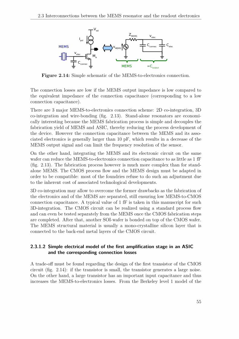
2.3 Interconnections between the MEMS resonator and the readout electronics
!"#$$%"
&'
()#*
+,,
&-&.
/%*%"
!"#$$%"
!%*%"
/%*%"
/&-&.
0&-&.
&-&. 1!#23)23
Figure 2.14: Simple schematic of the MEMS-to-electronics connection.
The connection losses are low if the MEMS output impedance is low compared tothe equivalent impedance of the connection capacitance (corresponding to a lowconnection capacitance).
There are 3 major MEMS-to-electronics connection scheme: 2D co-integration, 3Dco-integration and wire-bonding (fig. 2.13). Stand-alone resonators are economi-cally interesting because the MEMS fabrication process is simple and decouples thefabrication yield of MEMS and ASIC, thereby reducing the process development ofthe device. However the connection capacitance between the MEMS and its asso-ciated electronics is generally larger than 10 pF, which results in a decrease of theMEMS output signal and can limit the frequency resolution of the sensor.
On the other hand, integrating the MEMS and its electronic circuit on the samewafer can reduce the MEMS-to-electronics connection capacitance to as little as 1 fF(fig. 2.13). The fabrication process however is much more complex than for stand-alone MEMS. The CMOS process flow and the MEMS design must be adapted inorder to be compatible: most of the foundries refuse to do such an adjustment dueto the inherent cost of associated technological developments.
3D co-integration may allow to overcome the former drawbacks as the fabrication ofthe electronics and of the MEMS are separated, still ensuring low MEMS-to-CMOSconnection capacitance. A typical value of 1 fF is taken in this manuscript for such3D-integration. The CMOS circuit can be realized using a standard process flowand can even be tested separately from the MEMS once the CMOS fabrication stepsare completed. After that, another SOI-wafer is bonded on top of the CMOS wafer.The MEMS structural material is usually a mono-crystalline silicon layer that isconnected to the back-end metal layers of the CMOS circuit.
2.3.1.2 Simple electrical model of the first amplification stage in an ASICand the corresponding connection losses
A trade-off must be found regarding the design of the first transistor of the CMOScircuit (fig. 2.14): if the transistor is small, the transistor generates a large noise.On the other hand, a large transistor has an important input capacitance and thusincreases the MEMS-to-electronics losses. From the Berkeley level 1 model of the
55

Chapter 2 MEMS resonators and their readout electronics
10−18
10−16
10−14
10−12
10−10
10−8
10−6
10−4
10−2
100
102
Equivalent MEMS output capacitance [F]
Am
plif
ier
pow
er
consum
ption [W
]
Resistive MEMS output impedance
Capacitive MEMS output impedance
Cconnec
=100fF
Cconnec
=10pF
Cconnec
=1fF
Figure 2.15: Optimal amplifier power consumption versus equivalent MEMS out-put capacitance
transistors [Sansen 2006], it is possible to determine the optimal transistor dimen-sions and the corresponding optimal power consumption. The Gate-Source capac-itance is expressed as Cgs = 2
3CoxWALA where Cox, WA, LA are respectively the
oxide capacitance per unit of area, the width and length of the transistor. It resultsin a connection loss of:
Hconnec =1
1 + j2fifoscZMEMS
1Cconnec + 2
3CoxWALA
2 . (2.36)
Note that in (2.36), the effect of the Gate-Drain capacitance was neglected whichis correct only if the gain of the amplifier and the transistor length are small. Thisassumption should be verified for the considered CMOS design kit and the amplifiertopology. The PSD of the electronic noise expressed at the input of the transistoris (if only the white noise is considered):
SMA=
8kBTLA
3µNCoxWAVdssat
, (2.37)
where µN and Vdssat are the mobility and the Drain-Source saturation voltage of thetransistor, respectively. The corresponding signal-to-noise ratio expressed at thetransistor’s input is:
SNR =v2
MEMSTmeas
SMEMS + 8kBT LA
3µN CoxWAVdssat
---1 + j2fifoscZMEMS
1Cconnec + 2
3CoxWALA
2---2 .
56

2.3 Interconnections between the MEMS resonator and the readout electronics
(2.38)
In order to optimize the SNR, the second term in the denominator should be min-imized:
8kBTLA
3µNCoxWAVdssat
----1 + j2fifoscZMEMS
3Cconnec +
2
3CoxWALA
4----2
=
8kBTL2A
3µNCoxVdssat¸ ˚˙ ˝only depends on LA
---1 + j2fifoscZMEMS
1Cconnec + 2
3CoxWALA
2---2
WALA¸ ˚˙ ˝only depends on WALA
(2.39)
LA should therefore be taken to its minimum value Ltech imposed by the CMOSdesign rules while the transistor active area WALtech should be optimized:
WA =
Y][
3Ô
1+(2πfoscCconnecRMEMS)2
4πfoscCoxRMEMSLtechif ZMEMS = RMEMS
3(Cconnec+2CMEMS)2CoxLtech
if ZMEMS = 1j2πfoscCMEMS
. (2.40)
It is also quite common to analyze the power consumption of the circuit Pamp =Vdd
µN Cox
2WL
V 2dssat, where Vdd is the supply voltage of the CMOS technology. Based
on the HCMOS9 design kit from ST Microelectronics, the figure 2.15 presents theevolution of the amplifier power consumption for the optimal dimensions (WA givenby (2.40) and LA = Ltech) versus the equivalent MEMS output capacitance i.e1/ (2fifoscZMEMS). If the MEMS output impedance is purely capacitive then theresults presented in fig. 2.15 are independant of fosc. Otherwise, the equivalentoutput capacitance should be evaluated with respect to fosc. From fig. 2.15, wesee that in some cases, the optimal power consumption is too large for practicalapplication. Figure 2.16 depicts the corresponding MEMS-to-electronics connectionlosses versus the equivalent MEMS output capacitance. In the figure, the blue,green and red regions represent the typical range of the output capacitance of thecapacitive, piezoelectric and crossbeam detection scheme.
2.3.2 Interconnection schemes
The previous study highlights the interest of 2D- or 3D-integration of the MEMSand its associated electronics especially for capacitively-transduced resonators. Thefollowing subsections aim at refining the model of the connection losses in the case ofwire-bonding and 2D or 3D co-integration. The technological flow associated witheach connection scheme is described, as well as their associated equivalent electricalmodels.
57

Chapter 2 MEMS resonators and their readout electronics
Figure 2.16: NEMS-to-electronic connection losses versus the equivalent MEMSoutput capacitance. The crosses represent Hconnec for a resonator with a resis-tive output impedance and the circles represent Hconnec for a resonator with acapacitive output impedance.
!"#
$%&'()*
$%
!"#$$%$&'()#*+#,%-)&.
+,-(.-%/0&1%234'/05%06
73-3,-%/0&1%234'/05%06
/'(01()#*%,12
3&(&'()#*%,12
8'/9
:'/05%06
;<('
;).-
=(-(.)
=3-.)
>3)3,
;<('
>.,-
Figure 2.17: Simplified representation of a stand alone MEMS resonator and itsconnection pads (not to scale).
58

2.3 Interconnections between the MEMS resonator and the readout electronics
!"#
$%&'()*
$%
+,-%.%/0&12.(1.%,3&
40.02.%,3
5',6
7',38%39
:-('
:)1.
;(.(1)
;0.1)
<091.%/0&12.(1.%,3&
5',6
=/12. >/
12.
;(.(1)?0)02
Figure 2.18: Cross-section represen-tation of a stand-alone MEMS withdifferential actuation
!"#
$%&'()*
$%
+,-(.-%/0&1%234'/05%06
73-3,-%/0&1%234'/05%06
8'/9
:'/05%06
;<('
;).-
=(-(.)
"9>53=3-.)?
=3-.)@
8/9 8
3563
A%.
A3)3,
A.,-
Figure 2.19: Cross-section represen-tation of a stand-alone MEMS withshielded actuation
2.3.2.1 Stand alone MEMS connected to the electronics by wire bonding
One of the simplest methods to fabricate MEMS resonators is to start from a SOI-wafer5. These resonators are defined using only the top silicon layer. The geometryof the resonator is realized using a lithography step and an anisotropic etching. Theresonator is then released using the BOX (buried oxide) layer of the SOI-wafer as asacrificial layer and an isotropic wet or gaseous etching (fig. 2.17). See for example[Mile 2010].
The resonator is connected to the electronics via pads. Such pads are large conduc-tive areas in doped silicon or in metal on which a thin wire (named “bonding wire”)can be welded and its other extremity connected to the electronics. For the wire tobe properly bonded, the pad area is usually taken to 100 ◊ 100 µm2 or more. In thecase when the silicon is not very much doped, so as to improve piezoresistive detec-tion of the MEMS resonator, the resistance of the path between the pads and theMEMS electrodes can be large. To reduce the corresponding resistances, it is thencommon to add a metal layer on top of the pads and on the paths from the pads tothe MEMS electrodes. Knowing the area of the pads and of the paths, it is possibleto determine a capacitance CBOX of the BOX layer (fig. 2.17). Generally, the bot-tom face of the silicon bulk is connected to the ground and a resistance Rsub from theBOX/silicon bulk interface to the ground should be included in the electrical model.A resistance Rlat can be defined between the two capacitance CBOX correspondingto the actuation and detection pads. Finally the bonding wires can act as trans-mission and reception antennas, and be modeled by an inductance Lbonding with amutual coefficient Mbonding between each of them. Lbonding and Mbonding depend onthe length of the wires, the distance and the angle between each of them.
In differential actuation schemes, the two actuation pads and paths are symmetri-cally designed (fig. 2.18). The voltages on each actuation pad are in counter-phase
5http://www.soitec.com/fr/
59

Chapter 2 MEMS resonators and their readout electronics
105
106
107
108
109
−40
−35
−30
−25
−20
−15
−10
−5
0
5
MEMS resonance frequency [Hz]
|Hconnec| [d
B]
105
106
107
108
109
−40
−20
0
20
40
60
80
Sig
na
l−to
−b
ackg
rou
nd
ra
tio
[d
B]
Single actuation
Differential actuation
Shielded actuation
Analytical model
Figure 2.20: SPICE simulations of |Hconnec| and SBR versus the MEMS resonancefrequency for different actuation implementations of a crossbeam resonator. Thecurves in dashed lines depict the analytical formulas.
so that their feed-through contribution cancel each other at the MEMS output.Note that it is not necessary for the resonator to have a differential actuation as thefeed-through analyzed in this section is created from the MEMS-to-electronics accessand not in the resonator itself. In the case of a resonator with single-sided actuation(such as in a clamped-clamped beam with capacitive detection of subsection 2.2.1)the second pad and path are in an open-circuit configuration. A feed-through canhowever appear because of dispersions in the bonding wires or in the area of thepads and paths.
Another technique to reduce feed-through is to use a second layer of metal. Theactuation path is then realized using the top layer of metal while the lower metallayer is grounded (fig. 2.19). The latter metal layer acts like a shield preventing theactuation voltage from being transmitted to the substrate. This however increasesthe capacitance Cox between the actuation path and the ground because the oxidelayer between metal layers tends to be thin in CMOS processes. The capacitancecan be increased by a factor two to three compared to the BOX-capacitance. Dueto fringing effects, a capacitance Cedge between the actuation path and the bulkremains but it is reduced by two or three orders of magnitude. The capacitance Cox
can be reduced by increasing the oxide thickness or adding a third metal layer whentechnologically possible (in this case the second layer is filled with an oxide layerand increases the distance between the metal 1 and 3).
60

2.3 Interconnections between the MEMS resonator and the readout electronics
For the connection scheme depicted in figure 2.17, the expression of velec can belargely simplified if the effect of the inductance is neglected and if it is assumedthat Rlat π Rsub (i.e. the distance between the actuation and the detection pathsis small compared to the thickness of the bulk) :
velec =
!1 + j2πf RlatCBOX
2
"vMEMS + j2πf ZMEMSCBOX
2 vact
1 + j2πf!
RlatCBOX
2 + ZMEMSCBOX
2 + ZMEMSCelec
"≠ (2πf)
2RlatZMEMSCBOXCelec
¥vMEMS + ZMEMS
Rlatvact
1 + ZMEMS
Rlat
11 + 2 Celec
CBOX
2+ j2πfZMEMSCelec
if 2πf ∫ 2
RlatCBOX
. (2.41)
Note that in the case of a differential actuation, a term ∆Rlat/Rlat is factored tovact in eq. (2.41) where ∆Rlat is the fabrication mismatch in Rlat or is a result ofa mismatch in the differential actuation. In the case of the implementation with ashielded actuation, the term CBOX is factored to vact in the first line of eq. (2.41) isreplaced by Cedge. The feed-through is thus reduced by Cedge/CBOX .
The signal-to-background ratio SBR can be expressed as:
SBR =
-----gMEMSHconnec
Hft
----- =
Y___]___[
gMEMSRlat
|ZMEMS | for a single-sided actuation
gMEMSRlat
|ZMEMS |Rlat
∆Rlatfor a differential actuation
gMEMSRlat
|ZMEMS |CBOX
Cedgefor a shielded actuation
.
(2.42)
If gMEMS is smaller than 1, it is clear that a feed-through reduction technique isnecessary to observe properly the resonance of the resonator.
Figure 2.20 presents, for different integration schemes, the evolution of |Hconnec|and of the SBR versus the MEMS resonance frequency. The parameters takenfor the simulations are given in table 2.2 and the MEMS parameters are those ofthe crossbeam resonator experimentally characterized in chapter 3). In the case ofdifferential actuation, 100 Monte-Carlo simulations were made with a 1%-standarddeviation on the dimensions except for the bonding wire length and the mutualinductance where a 10%-standard deviation was taken (it is considered that thebonding is less reproducible). The SBR represented in figure 2.20 corresponds tothe mean value of the SBR obtained through these simulations. In the case ofshielded actuation, Cegde/CBOX = 1%. Note that the chosen value of Celec = 7 pFincludes the electronic input capacitance (¥ 2 pF) and the capacitance of the PCBboard on which the resonator chip and the ASIC are bonded (¥ 5 pF). One cansee a good match between the simulations and equations (2.41) and (2.42) whichvalidates the assumptions made to obtain our formula.
One can see in equation (2.42) that the SBR is inversely proportional to ZMEMS.It is therefore interesting to design MEMS with low output impedance in order tosimplify the measurement of the MEMS resonance. Crossbeam resonators, thanksto piezoresistive detection and the usually small aspect ratio of the gauges, havea small output impedance, which in most cases is smaller than that of the other
61

Chapter 2 MEMS resonators and their readout electronics
parameter value
Wire length 5 mm
Pad area 100 ◊ 100 µm2
Path area 100 ◊ 10 µm2
Distance
between paths
20 µm
BOX thickness 145 nm
Bulk thickness 750 µm
Lbonding 5 nH
Mbonding 0.25 nH
CBOX 2.7 pF
Rsub 682 kΩ
Rlat 26 kΩ
ZMEMS 1.25 kΩ
gMEMS 1.18 ◊ 10≠2
Celec 7 pF
Table 2.2: Parameters of thestudy of the substrate coupling.
Figure 2.21: Connection losses versus theequivalent MEMS output capacitance.
MEMS resonators. The results presented in figure 2.20 are therefore a best casescenario, among the MEMS resonators. It therefore explains why there are, upto the author’s knowledge, no measurement of stand-alone MEMS resonators withsingle-sided actuation and homodyne detection6 at high frequency.
Finally, figure 2.21 depicts the evolution of |Hconnec| versus the MEMS output ca-pacitance: the evolution of |Hconnec| remains similar to the one obtained with thesimple model of subsection 2.3.1.
2.3.2.2 MEMS-CMOS 2D co-integration
The 2D co-integration process flow used in Leti starts with the fabrication of theresonator: the silicon is doped, the resonator shape is defined with anisotropic etch-ing, then the MEMS is released using isotropic etching, which removes the BOXlayer. The resonator is then protected with an oxide deposition. A standard CMOSSOI process flow is applied to fabricate the electronics next to the resonator. Theelectronics is then protected while the oxide layers over the resonator are removed.Isotropic etching is finally used to remove the oxide protecting the resonator andreleasing the structure. A minimum distance of a few micrometers should be taken
6The measured frequency is equal to the actuation frequency as opposed to down-mixing archi-tecture [Bargatin 2005].
62

2.3 Interconnections between the MEMS resonator and the readout electronics
!"!# $!%#
!"#$%
&!'
()*+,-.
()
/012342
5)3
632%
783)1 (0,84%
&!'
632%()
!"!# $!%#
&'())*)+,-.(/ 0(1*2.+3
/9!(4)84,)28#
9%23-*:
9%23-*;
Figure 2.22: Simplified illustration of a 2D-cointegrated MEMS/CMOS system.On the top view, the oxide layers and the bulk are not depicted
between the CMOS circuit and the MEMS resonator so that the electronics is notaffected by the resonator’s final release.
2D-integration makes it possible to suppress the actuation and detection pads ofthe resonator. The paths between the resonator and the CMOS circuit are thereforereduced and so is their parasitic coupling. One can estimate that the actuation pathsare a few tens of micrometers long over one micrometer wide. The detection pathis minimized and is about equal to 10 ◊ 1 µm2. With such dimensions, the signal-to-background ratio is increased as depicted in figure 2.23. The lower feed-throughmakes it possible to design oscillators using non-differential actuation. Differentialactuation can however be implemented to improve the signal-to-background ratio inthe case of resonators with larger output impedance (e.g. capacitive detection).
2.3.2.3 MEMS-CMOS 3D-integration
The 3D monolithic integration implemented in Leti consists in first fabricating theintegrated circuit using a standard CMOS process with two metal layers. AnotherSOI-Silicon wafer is bonded on top of the first wafer. The bulk substrate of thesecond wafer is then removed. The Si-layer of the second wafer is used to fabricatethe MEMS resonator. The underlying oxide layer is etched to release the structurewhile another oxide layer (in blue on fig. 2.24) is used to stop the release etchingfrom contaminating the CMOS circuit.
The electrical paths between the resonator and the sustaining electronic circuit arevery similar to 2D-integration. The major difference originates from the holes thatconnect the top silicon layer to the metal layer (fig. 2.24). They can introduce aserial resistance and inductance. However, the electrical simulations do not showany significant difference between 3D- and 2D-integration.
63

Chapter 2 MEMS resonators and their readout electronics
105
106
107
108
109
0
25
50
75
100
125
Sig
nal−
to−
backgro
und
ratio [
dB
]
MEMS resonance frequency [Hz]
Single actuation
Differential actuation
Figure 2.23: Feed-through gain in a 2D-integrated NEMS/CMOS oscillator
!"#$%
&'()*+,
-./0120
3'1
410%561'/ &.*62%
7!8
&'
7!8
%029'/:(;0.<'/:(+1#%6
=%01+(>
=%01+(?
!"#$
"%"$
Figure 2.24: Simplified illus-tration of a 3D-cointegratedMEMS/CMOS system
2.3.3 Heterodyne architectures
Heterodyne architectures take advantage of a nonlinearity in the MEMS actuation ordetection in order to acquire the resonator output signal at a different frequency thanit was actuated. With this measurement scheme the feed-through can be reducedas the resulting parasitic signal is at a different frequency than the detected signal.The connection losses can also be reduced if the resonator output signal is at a lowfrequency. On the other hand, the feedback electronic circuit can be more complexas it should modify the frequency of the resonator output signal.
One of the simplest heterodyne architecture uses a quadratic nonlinearity in theactuation or the detection scheme in order to obtain a resonator output signal attwice the frequency of the actuation signal. In the case of electrostatic actuation:
Fl (t) =Á0h
g2
CV 2
DC
2+
v2act
4+ VDCvact sin (2fift) ≠ v2
act
4sin (4fift)
D. (2.43)
If vact is at frequency fr/2 then Fl (t) has a frequency component at fr. If thedetection is linear, the resonator output signal is at fr while the actuation voltage isat the frequency fr/2 (fig. 2.25). However, the feed-through can not be completelycancelled out. For example, the electronics may not be purely linear and includea quadratic term. The feed-through signal at the input of the electronics wouldthen be up-converted to twice its frequency: fr. Moreover, quadratic terms mayalso be found in the resonator detection for instance (e.g. the self-heating effect in apiezoresistive element). Moreover, in a non heterodyne architecture, the voltage VDC
can be large so that vact can be reduced and thus a low feed-through at the input ofthe electronics can be obtained7. If the resonator is actuated quadratically, vact is
7It is considered that the product VDC ◊ vact is adjusted so that the actuation force correspondsto the critical actuation force.
64

2.3 Interconnections between the MEMS resonator and the readout electronics
!"#
!"#$%#&'()*&&+,'-.)&$&-/("#%-0
1'-/)2)*
(34 1
5657)2)*
(
!"#
$%%&'#()*+,(
-.-/
1*/)2)*
(34
Figure 2.25: Heterodyne ar-chitecture.
!"#
!"#$%#&'()*&&+,'-.)&$&-/("#%-0
1'-/)2)*
(13435
)2)6*
!"#
$%%&'#()*+,(
-.-/
1*/)2)*
(
1,%'0
)2)*(76*
Figure 2.26: Downmixing architecture.
chosen so that v2act/2 = VDCvact (i.e. the actuation force corresponds to the critical
actuation force). In this scenario, vact can be larger than in linear actuation and thusthe feed-through at the input of the electronics is also increased. Furthermore, thequadratic terms in the resonator transduction amplifies the noise because the signalis squared but the noise is multiplied by the signal (and not squared). Finally, if theresonator is embedded in a self-oscillating loop, the feedback electronics must dividethe input frequency by two (in order to close the loop). To the author’s knowledge,there is no linear circuit capable of achieving this task and thus a digital circuitmust be employed that can emphasize the colored noise as expressed in subsection1.3.1.4.
A more advanced heterodyne architecture described in [Bargatin 2005] is referredas the down-mixing architecture (fig. 2.26). It requires a 2-port resonator for whichthe voltage applied on the detection port is at a frequency slightly smaller thanthe actuation frequency: fdet = fact ≠ ∆f . The varying electrical component (aresistance for piezoresistive detection or a capacitance for capacitive or a piezoelec-tric detection) is biased by the voltage applied on this port. The resonator outputsignal includes a term at the frequency ∆f . The frequency difference ∆f can bevery small, which simplifies the electronic design and reduces the connection lossesin the case of resistive detection. However, as for the previous heterodyne archi-tecture, the nonlinearity or the electronics of the MEMS resonator can also createsome feed-through. Consider for instance, the quadratic term in the electronics.The feed-through introduces, at the electronics input, frequency terms at fact andfact ≠∆f . The quadratic term in the electronics response can mix the two frequencyterms resulting in another signal at ∆f . Overall, heterodyne architecture usuallyhave smaller feed-through than homodyne ones.
2.3.4 Conclusion on MEMS-to-electronics interconnections
This section has described the major types of MEMS-to-electronics connections,their technical challenges and their impact on the sensor performance. 2D co-
65

Chapter 2 MEMS resonators and their readout electronics
integration presents optimal performances but is difficult to fabricate. Stand-aloneMEMS connected to the electronics by wire-bonding have simple fabrication pro-cess but the performances of the sensor are limited by large connection loss and highfeed-through. 3D co-integration is technologically challenging because two wafersmust be assembled together. However, it has the advantage of decoupling the fab-rication process of the CMOS circuit from the MEMS resonator and, thus, makesthe fabrication process of the resonator more flexible.
In the subsection 2.3.1, a simple model of the parasitic introduced by the connectionswas presented. Based on the proposed model a methodology was defined to designthe electronics and to evaluate the sensor performances.
2.4 MEMS resonators mass resolution comparison
2.4.1 Model presentation
From (i) the system architecture description of self-oscillating loops presented inchapter 1, (ii) the electrical description of the MEMS resonator, and (iii) the modelof the MEMS-to-electronics connection of section 2.3.2, it is possible to theoretically
!"#$%"&'()
!"#$*+,()
-%".(/01(#(+.2'#3
4/#&1+1(0/2%"&'()
5&36(2"73%+.+(23#/#$"("/1
892:"/+;+.#(+0&20;2()"2,+$"&1+0&1
<92="("/$+&#(+0&20;2!"#$>2!
%&#'">2!
(&$2#&,2)
*+*,2;/0$2
1".(+0&12<982#&,2<9<98
?92 ="("/$+&#(+0&2 0;2 #.(6#(+0&2 @0%(#'"2 ;0/2 ()"2$#7+$6$2$".)#&+.#%2,+13%#."$"&(
A92 ="("/$+&#(+0&2 0;2 ()"2 (/#&1+1(0/2 *+,()2 ;/0$216B1".(+0&2<9?989<2
C92="("/$+&#(+0&20;2!#-..&#
2#&,2!/$2;/0$216B1".(+0&2
<9?9<
D92 ="("/$+&#(+0&2 0;2 ()"2 E%%#&2 ,"@+#(+0&2 ;/0$21".(+0&12 8989<>2 89<>2 89?989<>2 89?989?>2 89?989A>2 <982#&,2 <9<98>2 +&.%6,+&'2 ()"2 ;%+.F"/2 &0+1"2 #&,2 ()"2;/"G6"&.H2,/+;(
I92="("/$+&#(+0&2 0;2 ()"2B"1(2$#112 /"10%6(+0&2 #&,2()"2.0//"130&,+&'2+&("'/#(+0&2(+$"
J92:"/+;+.#(+0&20;2()"2%+&"#/2/"130&1"20;2()"2K-KL
M92N1.+%%#(+0&23011+B%"2O
=PK>2K-KL2#13".(2/#(+0
K-KL2(030%0'H2#&,2(/#&1,6.(+0&>G6#%+(H2;#.(0/
K#7+$6$2#.(6#(+0&2@0%(#'"
K#7+$6$2QKNL2.6//"&(
K-KLRQKNL2.0&&".(+0&
-%".(/01(#(+.2#&,2=6;;+&'2&0&%+&"#/+(H
K#112/"10%6(+0& ="1+'&2.0&1(/#+&(1
,012S28
Figure 2.27: Simplified illustration of the function to determine the optimal designfor a clamped-clamped beam with capacitive detection.
66

2.4 MEMS resonators mass resolution comparison
assess the mass resolution of the MEMS-based sensor. The gain of the MEMS-actuation and detection transduction techniques and the MEMS-to-CMOS connec-tion topologies can be compared and the performance improvement of using a morecomplex integration scheme as presented in section 2.3 can be evaluated.
The proposed methodology is based on an optimization routine that seeks for thebest design (in terms of mass resolution) of the MEMS resonator and the CMOScircuit. The presented results are based on the SOI-65nm CMOS technology fromSTMicroelectronics. This CMOS-process is one of the most aggressive analog tech-nologies that make it possible to design compact, low-noise and high frequencyelectronic circuits. If the same design rules are used for the MEMS fabrication, thelithography rules of the process makes it possible to design MEMS resonators withnanometer dimensions that “should” enhance their performances.
The optimization routine uses several input variables that should be optimized. As-sociated with those variables other implicit parameters are determined from thedesign rules described in the previous sections. Example of implicit variables arethe integration time, the actuation voltage or the transistor width, the latter beingdetermined from subsection 2.3.1. The optimization routine is bounded by severalconstraints imposed by the fabrication and the environmental properties. Exam-ples of such constraints parameters are the MEMS resonator topology, the MEMS-to-electronics connection, the fabrication process and the associated DRM8 or thequality factor of the resonator. The figure 2.27 presents the input variables andthe design constraints for a clamped-clamped beam with capacitive detection. Asimplified description of function used to evaluate the mass resolution and thus todetermine the optimal design variables is also depicted in the figure.
The aspects considered in the model of the sensor performance are listed below:
• The electromechanical MEMS resonator response is based on the model pre-sented in sections 2.1, and 2.2.
• The electrical behavior of the MEMS-to-CMOS connection and the electroniccircuit is based on the model presented in section 2.3. The width of thetransistors is determined from eq. (2.40).
• The feed-through is modeled as described in section 2.3 and its effect on thefrequency-resolution was modeled as presented in section 1.1.2. The cases ofsingle-sided and differential actuation are evaluated.
• The electronics harmonic distortions are taken to ≠40 dB corresponding tosimulations on a typical low-distortion electronic circuit. The harmonic dis-tortions of the MEMS (if any) are based on the model of section 2.2.
• The noise sources considered in this work regarding the resonator are thethermomechanical noise, the Johnson noise and 1/f -noise in the piezoresistiveelements (if any); regarding the circuit the white- and flicker-electronics noiseat its input and the flicker noise at the electronics output.
8DRM stands for Design Rule Manual of the considered fabrication process
67

Chapter 2 MEMS resonators and their readout electronics
• The frequency drift of the sensors is modeled for a 0.1°C-temperature devia-tion. The corresponding coefficient is taken constant and equal to 100 ppm.
• Based on the white and flicker noise, the harmonic distortion and the frequencydrift, the maximum integration time is calculated.
• The effect of the temperature in the piezoresistive elements (if any) of theresonator is modeled based on analytical modeling.
The constraints imposed on the optimization routine are listed below:
• The lithography rules for the MEMS and the electronics design are based onthe SOI-65nm Dkit from STMicroelectronics.
• The thickness of the resonators is imposed by the process flow.
• A maximum voltage of 1 V is taken for the AC-value of the electrical signal.The polarization current of the first electronic amplifier is taken to 1 mA.
• The current density in the piezoresistive elements is limited to a value lowerthan the melting point of the material.
• Boundaries on the MEMS resonator actuation are taken so that the resonatorresponse can be considered as linear: in the case of electrostatic actuation,the mechanical displacement is ten times smaller than the gap. In the caseof duffing nonlinearity, the equivalent stiffness is ten times smaller than thebeam stiffness.
• It is ensured that the signal-to-noise ratio within the bandwidth of the res-onator is larger than 1.
This approach is necessary to compare the transduction mechanisms previously citedin this document: because they uses different physical properties and with differentdimensions, it is difficult compare them objectively.
Finally it should be recognized that the results provided in this section are subject tosome limitations as in all models. The purpose of the work presented in this sectionis mostly to give an impartial comparison of the performances of varous MEMStopologies. The performances of the sensors should be taken with some reserve butcan be used to provide an order of magnitude of the expected mass resolution. Themajor limitations of the modeling are listed below:
• The quality factor in vacuum is considered constant (i.e. Q = 1000) for everyresonators and for all dimensions. The crossbeam measured at Leti tendsto have a quality factor around Qcrossbeam ¥ 5000 while the quality factorof the nanowires are around Qnanowire ¥ 1000 due to its higher aspect ratioand the one of piezoelectric can be lower because of residual stress betweenthe layers of the cantilever. Moreover the quality factor tends to reduce atsmall dimensions, because the more aggressive fabrication process degradesthe mechanical properties of the MEMS layers.
68

2.4 MEMS resonators mass resolution comparison
10−6
10−5
10−4
10−22
10−20
10−18
10−16
Beam’s length [m]
Ma
ss r
eso
lutio
n [
g] Stand alone beam with
capacitive detection
Co−integrated beam withcapacitive detection
Stand alonecrossbeam
Co−integratedcrossbeam
Nanowire bothstand alone orco−integrated
Co−integrated piezoelectric cantilever
Stand alone piezoelectric cantilever
Figure 2.28: Graphic representation of the theoretical mass resolution versus thebeam’s length.
• Only the second harmonic distortion of the electronics was considered in themodel. Moreover it was considered as constant over the dimensions of the elec-tronic circuit. Finally, the flicker noise at the electronics output was supposedconstant and equal to
ÔSact = 1 µV/
ÔHz at 1 Hz.
• The doping level of the piezoresistive elements was taken constant and equalto 1019 cm≠3. The values of the doping-depend coefficient are based on char-acterizations: “Si = 160 , ΦSi0 = 10≠4 Ω/m, ŸH = 10≠5.
2.4.2 Results and discussions
As can be seen table 2.3 gives the results of the optimization presented in theprevious subsection and figure 2.28 depicts the evolution of the theoretical massresolution for a varying beam length. The connection losses of the MEMS resonatorusing capacitive detection are very important. The large connection losses reducethe signal-to-noise ratio and make the device very sensitive to feed-through. As amatter of fact, the latter issue limits the dimensions of the resonator. Differentialactuation or any other mean of feed-through cancellation are therefore crucial toincrease the signal-to-background ratio, reduce the dimensions of the resonator andthus improves its mass resolution. It should also be emphasized that due to thelarge connection losses, the dominant noise comes from the electronic circuit (except
69

Chapter 2 MEMS resonators and their readout electronics
MEMS
topologyclamped-clamped beam with
capacitive detection
Crossbeam
Stand-alone Co-integration Stand-alone Co-integration
Length59 µm 17 µm 0.8 µm 0.8 µm
27µm 8.3µm 0.8µm 0.8µm
Width295 nm 295 nm 80 nm 80 nm
295nm 295nm 80nm 80nm
Gap110 nm 110 nm 110 nm 125 nm
110nm 110nm 125nm 125nm
Gauge length160 nm 160 nm
160nm 160nm
Gauge width80 nm 80 nm
80nm 80nm
Resonance
frequency
0.73 MHz 7.9 MHz 220 MHz 220 MHz
29MHz 38MHz 220MHz 220MHz
Mass-
resolution
400 zg 17 zg 0.35 zg 0.026 zg
78 zg 2.5 zg 0.029 zg 0.024 zg
Integration
time
12 s 1.7 s 0.34 s 0.27 s
6.5 s 0.7 s 0.32 s 0.27 s
Actuation gain331 µm/V 2.9 µm/V 16 nm/V 12 nm/V
14 µm/V 0.13 µm/V 12 nm/V 12 nm/V
Unloaded
detection gain
24 V/µm 24 V/µm 1.2 V/µm 1.2 V/µm
24 V/µm 24 V/µm 1.2 V/µm 1.2 V/µm
Connect.
losses
92 dB 63 dB 21 dB 0 dB
107 dB 69 dB 21 dB 0 dB
SNR77 dB 108 dB 121 dB 127 dB
80 dB 118 dB 123 dB 127 dB
Main source
noise
Electronic Thermomech. Thermomech. Thermomech.
Electronic Electronic Thermomech. Thermomech.
SBR4.7 dB 4.4 dB ≠10 dB 11 dB
11 dB 12 dB 28 dB 51 dB
Limiting factorFeed-through Feed-through Lithography Lithography
Feed-through Feed-through Lithography Lithography
70

2.4 MEMS resonators mass resolution comparison
MEMS
topologyNanowire 1-port piezoelectric cantilever
Stand-alone Co-integration Stand-alone Co-integration
Length79 µm 79 µm 64 µm 2.8 µm
79 µm 79 µm 50µm 1.8µm
Width295 nm 295 nm 2.8 µm 82 nm
295nm 295nm 80nm 80nm
Gap110 nm 110 nm
110 µm 110 nm
SiN thickness366 nm 110 nm
1800nm 180nm
Resonance
frequency
409 kHz 409 kHz 0.11 MHz 18 MHz
409 kHz 409 kHz 1.1MHz 21MHz
Mass-
resolution
10200 zg 10200 zg 13000 zg 1.3 zg
10200 zg 10200 zg 210 zg 0.53 zg
Integration
time
161 s 161 s 0.93 s 0.09 s
161 s 161 s 0.4 s 0.12 s
Actuation gain1.1 mm/V 1.1 mm/V 120 µm/V 1.1 µm/V
1.1 mm/V 1.1 mm/V 4.9 µm/V 0.58 µm/V
Unloaded
detection gain
Nonlinear Nonlinear 26 V/mm 5.1 V/µm
Nonlinear Nonlinear 0.2 V/µm 3.3 V/µm
Connect.
losses
10 dB 0 dB 25 dB 34 dB
10 dB 0 dB 57 dB 32 dB
SNR5.2 dB 5.2 dB 161 dB 178 dB
5.2 dB 5.2 dB 163 dB 168 dB
Principal noiseJohnson Johnson Thermomech. Thermomech.
Johnson Johnson Electronic Thermomech.
SBR0 dB 0 dB
2 dB 29 dB
Limiting factorLow vMEMS Low vMEMS Feed-through Feed-through
Low vMEMS Low vMEMS Feed-through Form factor
Table 2.3: Comparison between different MEMS topologies. The results in boldcorrespond to resonators with differential actuation, the other corresponds to asingle-sided actuation.
71

Chapter 2 MEMS resonators and their readout electronics
for the co-integrated resonator with single-sided actuation). Note finally, that theunloaded capacitive gain of the resonator is large but is degraded by the connectionlosses.
The crossbeam resonator features much lower detection losses thanks to its piezore-sistive detection. The crossbeam can then be designed with its lowest dimensions.However, when the crossbeam dimensions are small, the beam becomes stiff andthe actuation voltage, that provokes a mechanical displacement to a tenth of theelectrode’s gap, is large and emphasizes the electrostatic nonlinearity: it reducesthe maximum integration time. Overall, the mass resolution improves only moder-ately if the resonator dimensions are reduced by a certain point. It should finallybe underlined that the large signal-to-noise ratio of this resonator topology makesthe characterization of the device simpler. As a matter of fact, the mass resolu-tion announced by the model is much better than the state-of-the-art but it will beshown in the chapter 3 that a large flicker noise introduced by the resonator limitsits frequency resolution.
The nonlinear detection of the piezoresistive nanowire emphasizes the noise sourcesin the oscillator. The resonator is actuated at fr but its output signal frequency is2fr. Moreover, while the resonator output signal is proportional to the square of themechanical displacement, the noise at the output of the resonator is proportional tothe product of the thermomechanical noise with the mechanical displacement. Thenoise and especially the close-to-carrier colored noise is amplified by the nonlinearitymaking it difficult to shrink the dimensions of the resonator. Note finally that theresonator presented in table 2.3 has a very large length-to-thickness aspect ratioand thus a low stiffness in the out of plane direction. The release of the mechanicalstructure will thus probably be critical.
Piezoelectric cantilevers use a linear actuation and detection transduction tech-nique, which makes them more insensitive to nonlinearity and thus to flicker noise.If a bridge architecture is used, the intrinsic feed-through provoked by the AlN-capacitance is reduced and resonators with smaller dimensions can be designed.The piezoelectric actuation and detection scheme exhibit a large gain making ispossible to achieve large resonator output signals and (very) large signal-to-noiseratio, thus improving the mass resolution of the sensor. If a piezoelectric cantileveris co-integrated with a CMOS-circuit and uses a differential actuation, its massresolution should reach state-of-the-art mass resolution [Jensen 2008]. However,the implementation of piezoelectric resonators co-integrated with a CMOS-circuit istechnologically very difficult.
Overall, the study shows that the resonators with capacitive detection suffer fromfeed-through and high connection losses making it difficult to operate them at lowdimensions. The nanowire performances are poor due to the frequency aliasing inthe nonlinear detection transduction making the considered topology unadapted forclosed-loop mass measurement. Finally the two most promising candidates for massmeasurement are the crossbeam and the piezoelectric cantilever. The former can
72
2.5 Collectively addressed MEMS arrays
be fabricated with ease but suffers from an actuation transduction that introduceslarge harmonic distortion thus emphasizing the colored noise and limiting the mass-resolution of the sensor. The piezoelectric resonator has linear electromechanicaltransduction, which improves the mass-resolution of the oscillator. The topology ishowever difficult to fabricate and has a large intrinsic feed-through.
2.5 Collectively addressed MEMS arrays
It is usually admitted that implementing MEMS resonators in collectively addressedarray increases the SNR because the output signals of the resonators add up in acoherent way, whereas their output noises add up in a statistical way[Ekinci 2004a].The SNR should therefore increase with the number N of resonators in array ac-cording to SNR Ã N . However, there is still no example in the literature of CMOS-integrated MEMS array and only a limited number of stand-alone MEMS arrayrealizations [Lee 2004, Bargatin 2008, Kharrat 2009]. The resonators should how-ever be identical and the added mass to be measured should be introduced depositeon each resonators.
Nevertheless, to what extent arrays improve the SNR has never been analyzed indetail. In this section, we demonstrate that the intrinsic electrical behavior of theresonator and its surrounding environment determine an upper limit of the SNR. Thecase of co-integrated MEMS/CMOS and stand-alone MEMS arrays are studied. Forthese configurations, the SNR is studied as a function of the number of resonators.The best achievable SNR and the optimum number of MEMS resonators are alsoanalytically determined.
Subsection 2.5.1 focuses on the determination of the total gain of the MEMS arrayand its readout electronics. The signal-to-noise ratio at the electronics output andthe minimal number of MEMS resonators to reach the best performance are de-termined in subsections 2.5.3 and 2.5.2. Finally the previous analytical results arecompared with SPICE-simulations in subsection 2.5.4.
2.5.1 Amplification gain
An array of N MEMS resonators connected in parallel is depicted in figure 2.29. Theoutput electrical signal of each device is summed into the input of the electronicsas shown in figure 2.29. The transistor is biassed by an ideal current source. Cload
represents the input capacitance of the following electronic stage (e.g. a bufferstage). Its typical value is Cload = 100 pF.
The output voltage of each resonator drives its own output impedance ZMEMS,the on-chip routing parasitic capacitance Cp, the capacitance of the MEMS-to-electronics capacitance Cconnec divided by the number of resonators (depending
73

Chapter 2 MEMS resonators and their readout electronics
!"#$$%"
&'
!(#)*
+*,
-**
.#/0
&1&2345
&1&2346
!!!
!"#$ .
%(%"
!"#$
!!!
!7 !
8,
%&'
89:
.%(%"
8*,
!(#)*
.#/0
.%(%"
"#$%&'()*%+
(&)&%
*
+&)&%
,("#$
-&)&%
&1&2345
-./
%&)&%
1(%"0;#$<",0)8%36
%%0'1)2
!7
(&)&%
*
+&)&%
,("#$
-&)&%
&1&2346
-./
%&)&%
!"#$$%"
Figure 2.29: Schematic of the MEMS array and its readout electronics.
74

2.5 Collectively addressed MEMS arrays
on the MEMS/CMOS connection configuration: for MEMS/CMOS co-integrationCconnec = 0, for wire-bonding connection Cconnec = 10 pF, for coaxial cable connec-tion, Cconnec = 100 pF) and the input capacitance of the electronics also divided bythe number of resonators. The small signal drain-source current produced by thetransistor flows into its intrinsic admittance and Cload.
The transistor is modeled with the Berkeley level 1 model [Sansen 2006]. Its dynamicbehavior is described by an input capacitance Cgs, a transconductance gm and anoutput admittance gds. Note that the feedback capacitance Cgd has been neglectedin order to simplify the study. This assumption is only valid in case of low-gainamplifiers and should be verified with the design kit. The Drain-Bulk capacitanceCdb can be neglected compared to Cload: Cdb π Cload. The MEMS gain velec
vactcan be
calculated from the sum of the MEMS output voltages:
velec = NHMEMS (f) vact1/ZMEMS
N/ZMEMS + j2fif (NCp + Cconnec + Cgs). (2.44)
Hence
velec
vact
=NHMEMS (f)
N + j2fifZNEMS (NCp + Cconnec + Cgs). (2.45)
Then the total gain G = vout
vactcan be deduced:
G =
------≠gmHMEMS(f)
[gds + j2fifCload]Ë1 + j2fifZMEMS
1Cp + Cconnec+Cgs
N
2È
------. (2.46)
Assuming that the amplifier is properly designed (i.e. gds ∫ 2fifCload), the totalgain has the following expression:
G =
--------
HMEMS(f)
1 + j2fifZMEMS
3Cp +
Cconnec+ 23
CoxWALA
N
4
--------
2LA
KeN (Vgs ≠ VtN)
G ≠æNæŒ
-----HMEMS(f)
1 + j2fifZMEMSCp
-----2LA
KeN (Vgs ≠ VtN). (2.47)
We make the assumption that N is large enough so that the admittance of (Cconnec + Cgs) /Ncan be neglected compared to the equivalent admittance of Cp and ZMEMS: 2fif (Cconnec + Cgs) /N πÒ
(2fifCp)2 + 1/Z2MEMS.
75

Chapter 2 MEMS resonators and their readout electronics
2.5.2 Signal-to-noise ratio optimization
The noises in this architecture arise from the MEMS devices, the transistor and thefollowing electronic stage. The noise at the output of the MEMS device (thermome-chanical noise and Johnson noise) is modeled with a voltage PSD of SMEMS. Thevoltage PSD of the noise produced by the transistor on its gate is SMA
= 8kBT3gm
. Thefollowing electronic stage at the transistor drain has a voltage PSD of SST AGE2 =15 nV/
ÔHz
22. This value is typical for a measurement equipment, (e.g. the SR830
lock-in amplifier) or a commercial amplifier. It can also be reached with ease in anintegrated circuit. Flicker noise is not considered in this subsection but the validityof this assumption will be confirmed in subsection 2.5.4. The SNR at the input ofthe electronics can be calculated:
SNR =
-----v2
elec
SMEMS+elec
----- =G2v2
act
SMEMS+elec
=
------HMEMS(fr)vact
1+j2πfrZMEMS
1Cp+
Cconnec+CgsN
2
------
2
Tmeas
SST AGE2
CKeN (Vgs ≠ VtN)
2LA
D2
+
¸ ˚˙ ˝STAGE2 æ iNEMS
8kBT
3gm¸ ˚˙ ˝MA noise
+SMEMS/N
---1 + j2fifrZMEMS
1Cp + Cconnec+Cgs
N
2---2
¸ ˚˙ ˝MEMS noise
.
(2.48)
Thus:
SNR ≠æNæŒ
--- HMEMS(fr)vact
1+j2πfZMEMSCp
---2
Tmeas
SST AGE2
ËKeN (Vgs≠VtN )
2LA
È2+ 8kBT
3gm
. (2.49)
For a given MEMS resonator and for a given implementation, the single way to
optimize the SNR is to minimize the term SST AGE2
ËKeN (Vgs≠VtN )
2LA
È2+ 8kBT
3gm. In other
words, implementing MEMS resonators in arrays reduces the MEMS noise-to-signalratio by a factor N to the point that it can be neglected compared to the electronicnoise. Note that if the electronic noise sources are not considered, the signal-to-noise
ratio is then, as expected, equal to N---HMEMS(f)vact
SMEMS
---2
Tmeas.
Since the effect of the interconnection capacitance and of the input capacitance ofthe electronics is negligible when N is large, the SNR can be made arbitrarily largeby designing electronics with large LA and gm. However, a limitation is alwaysimposed by the maximum polarization current Imax and as a matter of fact, thevoltage power spectral density of the transistor noise on its gate has a finite value:
76

2.5 Collectively addressed MEMS arrays
Cconnec 0 1 pF 10 pF 100 pF
Nmin≠cap 1 2 20 196Nmin≠noise 5 4 1 1
Table 2.4: Minimal number of MEMS versus Cconnec
SMA= 4kBT (Vgs≠VtN )
3Imax. In a well-designed circuit, the following stage is designed
according to the input voltage noise and the voltage gain of the previous electronicstage, so that the input voltage noise of stage 2 is negligible compared to the outputvoltage noise of stage 1: SST AGE2 is neglected. In these circumstances, the maximumsignal-to-noise ratio is:
SNRmax =
-----HMEMS(fr)vact
1 + j2fifrZMEMSCp
-----
23ImaxTmeas
4kBT (Vgs ≠ VtN), (2.50)
2.5.3 Minimal number of MEMS resonators to reach the best
array performance
Equation (2.48) shows that implementing MEMS resonators in array reduces the ef-fect of Cconnec and Cgs. Indeed, the low-pass filter term in equation (2.48), is reducedby increasing N until it reaches |1 + j2fifrZMEMSCp|2. Assuming that the MEMS-noise is negligible (this hypothesis should be verified a posteriori), one can determinethe number of resonators N required to achieve close-to-maximal SNR by solvingthe following condition 1 + (2fifZMEMSCp)2 > (2fifr)
2 Z2MEMS (Cconnec + Cgs)
2 /N2.Thus:
Nmin≠cap >2fifrZMEMS (Cconnec + Cgs)Ò
1 + (2fifrZMEMSCp)2=
2fifrZMEMS
5Cconnec +
4IdsL2A
3µN (Vgs≠VtN )2
6
Ò1 + (2fifrZMEMSCp)2
.
(2.51)
Table 2.4 gives Nmin≠cap for several values of Cconnec and for a minimal transis-tor length of 0.13 µm. The values of the other parameters are given in table 2.5.Obviously Nmin≠cap increases with Cconnec.
One must then verify the a priori hypothesis that the noise of the MEMS resonatorscan be neglected. In other words, one must verify that the following condition issatisfied:
4kBT (Vgs ≠ VtN)
3Imax
∫ 1
N
SMEMS---1 + 2fifrZMEMS
1Cp + Cconnec+Cgs
N
2---2 . (2.52)
Equation (2.52) amounts to a second order equation, from which the minimal num-ber of MEMS resonators Nmin≠noise can be easily analytically deduced. The nu-merical results expressed in table 2.4 (Nmin≠noise criteria corresponds as previously
77

Chapter 2 MEMS resonators and their readout electronics
to a SNR-reduction of 3dB compared to SNRmax). For low values of Cconnec, the
term (2fifr)2
Z2NEMS
1Cp + Cconnec+Cgs
N
22in equation (2.52) is negligible compared to
1 and Nmin≠noise is governed by Nmin≠noise = 3Imax
4kBT (Vgs≠VtN )SMEMS. For high val-
ues of Cconnec, the capacitive attenuation diminishes the MEMS output signal, theMEMS noise becomes negligible and the minimal number of MEMS resonators inarray is determined from equation (2.51).
In fact, the two conditions imposed by Nmin≠cap and Nmin≠noise must be respected.Nmin≠cap tends to increase with ZMEMS and Cconnec contrarily to Nmin≠noise. ThusNmin≠noise tends to dominate for co-integrated resonators whereas Nmin≠cap tendsto dominate for stand-alone resonators.
2.5.4 Results, discussions
SPICE simulations of arrays were made for N from 1 to 100 000. The simulatedtransistor is taken from ST Microelectronics HCMOS9 design kit. The dimensionsof MA are optimized for each N and Cconnec based on the Berkeley level 1 model ofthe transistor. Its width was then adjusted in order to adapt to the more advancedSPICE model of the design kit.
The results in terms of SNR are given in figure 2.30 for several values of: Cconnec.The simulated MEMS resonator is a crossbeam [Mile 2010] (fig. 2.31a) with thedimensions given in table 2.31b.
The other parameter values are referenced in table 2.5. At the resonance frequency,HMEMS (fr) is calculated from [Arndt 2011]:
HMEMS (fr) = 3.83Á0“Si
cSi
QVDCVgl
g2bg
. (2.53)
The MEMS output signal increases with N and saturates to the limit HMEMS (fr) vact
(the voltage of the Thevenin model of the MEMS resonator). The MEMS outputsignal improvement with N reaches therefore a maximum. Moreover as N is getting
larger, the SNR increases as well as the value ( (HMEMSvact)2
SMEMS). Indeed, the signal
output of the MEMS array scales as N , whereas the standard deviation of the noisescales as
ÔN .
The two previously mentioned limitations (described by Nmin≠cap and Nmin≠noise)to the SNR of the MEMS array can be observed in figure 2.30. When Cconnec islower than 10 pF, the performance of the MEMS array is mostly driven by theMEMS noise sources and not by the MEMS output capacitance (Cconnec and Cgs).For larger values of Cconnec, the MEMS output capacitance strongly attenuates theMEMS output signal. In this case, the aim of implementing MEMS resonators inarray is to reduce the connection capacitance. Finally, the number of resonators
78

2.5 Collectively addressed MEMS arrays
100
101
102
103
104
105
106
60
70
80
90
100
110
Number of MEMS in array
SN
R (
dB
)
Cconnec
=
10 pF
Cconnec
=100 pF
Cconnec
=1 pF
SNRmax
obtained from
eq. (2.50)
Figure 2.30: SNR versus the number of MEMS for 3 values of the connectioncapacitance. The crosses (+) correspond to the simulated points and are linkedwith a line. The value of SNRmax is represented by the dashed horizontal line.
!"#$%#&'()*+*"#,'-*.
/*%0
1&*2',*.&.#&3*)4%$4*.
(a)
Parameter Value
Beam’s length L = 1.6 µmBeam’s width b = 130 nm
Beam’s thickness h = 50 nmGauge’s length lg = 100 nmGauge’s width bg = 50 nm
Electrode-beam gap g = 80 nm
(b)
Figure 2.31: Crossbeam MEMS: (a) SEM illustration, (b) dimensions of the res-onator
79

Chapter 2 MEMS resonators and their readout electronics
parameter value
Layout capacitance Cp = 10 fF
MEMS resonance frequency fr = 89 MHz
Resonator quality factor Q = 100
Air permittivity ε0 = 8.85 ◊ 10≠12 F/m
Silicon gauge factor γSi = 120
Silicon Young modulus cSi = 169 GPa
DC-actuation voltage VDC = 5 V
AC-actuation voltage vact = 1 V
Voltage applied on each gauge VS = 0.1 V
Resonator output voltage HMEMSvact = 1.0 mV
Resonator output impedance ZMEMS = 3.5 kΩ
Resonator thermomechanical noise Sthermo =1
5.5 nV/Ô
Hz22
Measurement time Tmeas = 1 s
Electronics maximum polarization current Imax = 100 µA
Transistor’s gate polarization voltage Vgs = 0.6 V
Threshold voltage VtN = 0.28 V
Electron mobility µN = 18 Vm2s≠1
SNRmax (see eq.(2.50)) 108 dB
Table 2.5: Study parameter values for a doping level of 1019 cm≠3
where the SNR reaches a limit on figure 2.30 shows a good correspondence with thevalues of table 2.4.
As shown by equation (2.50), the SNR for an infinite amount of MEMS resonatorsdoes not depend upon Cconnec. Clearly, for a sufficient number of MEMS devices,the SNR will be the same whether the resonators are co-integrated or not with theirreadout electronics.
The resistive behavior of the MEMS gauges introduces some flicker noise. However,from [Harkey 2000], the corner frequency of the flicker noise compared to the ther-momechanical white noise of the MEMS device (corresponding to the frequency atwhich the PSD of the flicker noise is equal to that of the thermomechanical whitenoise) is around 2.7 MHz. The corresponding Hooge noise coefficient was taken toŸH ¥ 10≠5. The corner frequency of the transistor used in the different simulationsfor a large MEMS array is 1.6 MHz. The low corner frequencies of the transistorand gauge flicker noise validates the hypothesis made in section 2.5.2 that the flickernoise can be neglected.
It should be highlighted that in this study, neither the technological dispersions, northe increase of Cp with N (arising from the complex layout routing that should beimplemented) have been modeled. The technological dispersions are likely to furtherreduce the performance of MEMS arrays. It is possible to use an analytical approach,
80

2.6 Conclusion
rather than costly Monte-Carlo simulations, to account for dispersions on the centralfrequency. This can be done using [Bargatin 2008] if the dispersions are assumed tofollow a Cauchy law, or [Kharrat 2009] in the case of a normal law. In the formercase, the standard frequency deviation ‡ = 1% results in a loss of 10 dB, whereas inthe latter case, the loss is only 7.2 dB. Note that the value of SNRmax reduces dueto dispersions as the quality factor of the resonators becomes larger. Nevertheless,these results still demonstrate the high interest of having MEMS connected in arraysespecially when a stand-alone readout electronics is used for which the connectioncapacitance are large.
2.5.5 Conclusion of collectively-addressed MEMS arrays
After introducing a simple electrical model of the MEMS resonators, an array ofMEMS devices all connected to a common amplifier was analytically studied. Itshows that the performance in terms of SNR of the MEMS array is larger than thatof a stand-alone MEMS resonator. However as N increases, the SNR of the arrayreaches a limit whether the array is co-integrated or not with its electronics. Thislimit was analytically studied and depends on the electronics input noise, the MEMSoutput signal and impedance. The minimal number of MEMS to achieve close tooptimal performance depends mainly on the connection configuration. Stand-aloneMEMS arrays are interesting candidates to improve the resonators performances upto ones of co-integrated MEMS/CMOS system without the cost of a specific processdevelopment. This study therefore provides a simple analytical assessment of thebest achievable performances.
SPICE simulations for an array of crossbeam MEMS resonator were performed.They show similar results to those predicted by the analytical study. They alsoshow that the SNR improvement is small (Æ 10 dB) for architectures with low con-nection capacitance as MEMS/CMOS co-integrated or 3D-integrated architecture.An improvement of 45 dB can be reached for stand-alone electronics configuration(where Cconnec ¥ 100 pF). Although the results presented here are based on a sin-gle active transistor circuit, one should expect similar results with more complexelectronics architecture (OTA, cascode...). Even by including possible technologicaldispersions, this would not change the overall results presented here
2.6 Conclusion
In this chapter the electromechanical behavior of various resonators was described.Different electromechanical actuation and detection transduction techniques werepresented using simple analytical expressions. Different MEMS-to-electronic con-nection implementations were presented and compared. Their intrinsic connectionlosses and feed-through were presented and techniques to improve the MEMS-to-electronic connections were proposed and evaluated.
81

Chapter 2 MEMS resonators and their readout electronics
These MEMS resonators were then compared based on the system architecture de-scription presented in chapter 1, the description of the MEMS resonator and theelectrical model of the oscillator. It was shown that the crossbeam resonator and thepiezoelectric cantilever are very promising candidates for mass sensing applications.Thanks to its simple technological fabrication and the possibility to co-integrateit with ease with a CMOS circuit, the clamped-clamped beam using a capacitivedetection is also an interesting candidate for minute mass sensing.
Finally the implementation of MEMS resonators in array was explored and theelectrical limits due to the CMOS circuit were determined. This study reveals amajor interest of array in the case where resonators are fabricated on a differentwafer than the CMOS circuit.
The following chapter presents different MEMS resonators and oscillators realizedand characterized during this PhD study.
82

3 Practical realizations
In this chapter, the design and the characterization of MEMS-based closed-loop os-cillators are presented. In section 3.1, the performance of two different self-oscillatingloops (one based on a piezoelectric cantilever, the other on a piezoresistive cross-beam) realized with discrete electronics is assessed. Section 3.2 describes the designof an ASIC to self-oscillate multiple stand-alone crossbeams. This ASIC uses bothanalog and digital electronics and is composed of sustaining electronic circuits andfrequency counters. On the same ASIC, this electronics was duplicated 4 times sothat 4 MEMS resonators can be controlled independently. Finally, the section 3.3describes the design and characterization of resonators integrated on the same waferwith their electronic circuit. Capacitive clamped-clamped beams and piezoresistivecrossbeams were co-integrated with a dedicated CMOS readout circuit.
3.1 Self-oscillating loops using discrete electronics
The realization of two self-oscillating loops with discrete electronics is hereby pre-sented. This type of electronics makes possible to quickly design and optimize oscil-lators but are limited in terms of flexibility and can introduce larger electronic noiseas it will be discussed. In a first part, the realization of an oscillator with a piezo-electric micro-cantilever is described. This resonator is actuated under atmosphericpressure in order to evaluate its potential for gas sensing (it will be shown that itsmass resolution is poor because of the large dimensions of the device). In a secondpart, the implementation of a piezoresistive crossbeam in a self-oscillating loop isdescribed. As opposed to the piezoelectric cantilever, the crossbeam is actuated invacuum to improve the signal-to-background ratio (working in vacuum is justifiedfor mass spectrometry applications).
3.1.1 Self-oscillating loop with a piezoelectric micro-cantilever
Hereby is described the design and the characterization of the self-oscillating loopwith a piezoelectric cantilever. First the dimensions and the fabrication process ofthe piezoelectric micro-cantilever are detailed. Then, a method on how to circumventthe feed-through intrinsic to piezoelectric resonators is proposed. This feed-throughreduction technique consists in using a variable capacitance and a variable resistanceimplemented in a bridge architecture. The overall topology of the oscillator is then
83

Chapter 3 Practical realizations
Figure 3.1: SEM caption of themicro-cantilever.
!"#$%&%'()"*%+$,(
-"((".$%&%'()"*%+$,(
,/%0"%&%'()/'$&12%)+$3&4
5&16(/'$&12%)+$7/4
89$:;<$=.>9;<$=. ?@$A.
@<$A.
:<<$A.
B<<$A.
Figure 3.2: Technological stack ofthe piezoelectric cantilever.
justified. In a third part, different frequency resolution measurement techniques toevaluate the performance of the self-oscillating loop are described and compared.Finally, the frequency resolution of the self-oscillating loop is compared with theone of an FLL-architecture.
3.1.1.1 Presentation of the piezoelectric micro-cantilever
The self-oscillating loop is realized using a 50 nm-thick AlN piezoelectric resonator(fig. 3.1). The resonating element is a micro-cantilever composed of the followingmaterial stack (depicted in figure 3.2) deposited on a standard silicon wafer (frombottom to top): 600 nm-thick silicon nitride, 100 nm-thick platinum, 50 nm-thickAlN, 25 nm-thick platinum. Fabricated with standard CMOS compatible, surfacemicro-machining technology [Ivaldi 2011b], the 140 ◊ 40 µm2-cantilever area is de-fined with two Ultra Violet lithography steps. A XeF2 plasma isotropic etchingtechnique is used to release the cantilever (the silicon bulk acts as a sacrificial layer).
With such dimensions, the resonance frequency is theoretically 42 kHz but wasmeasured at 36 kHz. The difference is believed to originate from a too aggressiverelease process, consequently part of the clamping area is also free-standing, i.e. lessrigid.
The measured resonator output voltage corresponding to a critical amplitude dis-placement of 100 nm is around 3 mV versus 4.2 mV obtained theoretically (see sub-section 2.2.4).
3.1.1.2 Feed-through reduction
In 1-port piezoelectric cantilevers, a major issue to deal with is the large intrinsicfeed-through introduced by the piezoelectric static-capacitance. Figure 3.3 depictsthe behavior of the equivalent capacitance of the micro-cantilever versus frequency:the useful signal is about 30-times smaller than the intrinsic feed-through. The most
84

3.1 Self-oscillating loops using discrete electronics
30 32 34 36 38 4033
33.1
33.2
33.3
33.4
33.5
33.6
33.7
33.8
Frequency [kHz]
Equiv
ale
nt capacitance [pF
]
2×∆C≈ 2 pF
Figure 3.3: Equivalent capac-itance of the PZE cantilevermeasured with a HP4194impedance meter.
103
104
105
106
10−4
10−3
10−2
10−1
100
Frequency [Hz]
Gain
of th
e b
ridge
Measurement with a7280−lock−in amplifier
Fit
Figure 3.4: Evolution of the MEMS+firstamplifier gain in the bridge implementation(see figure 3.6).
common feed-through reduction technique consists in implementing the resonator ina bridge architecture using an identical but unreleased micro-cantilever or a variablecapacitance to cancel the feed-through. We have chosen the implementation thatuses a variable resistance and capacitances because the feed-through could be furtherreduced around fr than when an identical unreleased cantilever is implemented.Indeed it is believed that the release affects the dimensions of the cantilever andcreates a mismatch between the static capacitance of the released and the unreleasedcantilever.
Moreover, the AlN-layer introduces non-null dielectric losses that can be modeledby introducing an imaginary part to CP ZE: CP ZE ¥ CP ZE (1 + jd) where d π 1represents the dielectric losses (measured to d ¥ 1%). They can be canceled byimplementing a variable resistance in parallel to the variable capacitances. Finally,the value of |CP ZE| varies with the frequency. Using an HP4194 impedance meter,one can model the evolution of CP ZE as:
CP ZE = CP ZE0
Af
fr
Bpft
(1 + jd) , (3.1)
where pft ¥ ≠4.4 ◊ 10≠3 (from measurements) is a fitting parameter and CP ZE0 =33 pF (from measurements) is the value of the AlN-capacitance at fr. The figure3.4 compares experimental data with the model of the bridge gain versus frequency.Therefore the model correctly describes the behavior of the bridge and the result-ing feed-through. The difference between the model and the measurement is dueto an imperfect adjustment of the variable components (the resistance or the ca-pacitances). Figure 3.5 depicts the measurement of the gain of the bridge aroundfr. One can see that the signal-to-background is close to 3 making it possible toimplement the micro-cantilever in a self-oscillating loop.
85

Chapter 3 Practical realizations
30 32 34 36 38 40−200
−150
−100
−50
0
50
100
Bridge p
hase−
shift [°
]
30 32 34 36 38 400
0.005
0.01
0.015
0.02
0.025
Frequency [kHz]
Bridge g
ain
fr=35.4kHz
pft=−15×10
−3
R0=4.2MΩ
C0=33.4pF
gMEMS
=7.8×10⁻³
Q=59
Figure 3.5: Gain and phase-shift of the bridge around the resonance frequency.
!"!#$%&
!"#$%&#'#()*"(+,+-
.'/0123/012456789!"#$%"#&'(
:*";<#=!4>6?7
)&**+,"-#$"#&'(
@A
&AB/*"/C'#D&.
E*"1'#3FG4HIA777
./01&*&-"#&'(
!/JJ"K#3L!M!(I?3NL$
23,3&1#4%&(5
!/JJ"K#3F!M!(IA73NL$
67"84987&*#&(5"(:,;3,*&1#4%&(5
Figure 3.6: Simplified schematic of the self-oscillating loop.
3.1.1.3 Topology of the self-oscillating loop
The attenuation introduced by the MEMS resonator is compensated using a low-noise ADA4817 commercial amplifiers with large bandwidth. The MEMS-to-electronicsconnection losses are minimized by connecting the first amplifier very close to theMEMS resonator. The resulting connection capacitance is estimated to be smallerthan 10 pF. The oscillation amplitude in closed-loop is controlled using an AD8036clamping amplifier. The major challenge in the design of the loop is to filter the feed-through out of fr: figure 3.5 shows that below and higher than fr, the feed-throughsignal is larger than the resonance signal. Figure 3.5 shows that the phase-shiftvaries from +90°1 to ≠180°, what can be explained by the fact that the static ca-pacitance CP ZE is smaller than the variable capacitances at high frequency. Thephase-shift at the resonance frequency is around ≠90°. In order to respect the os-cillating conditions, the phase-shift should be translated up by +90° so that theoverall open-loop phase-shift is 0° at fr. The corresponding phase-shift should thenvary between +180° and ≠90°.
To avoid at low-frequency that the phase-shift is equal to n◊2fi (n is an integer), theorder of the high-pass filters should be equal to 1. At high-frequency, the phase-shiftis lower than ≠90° preventing also the low-pass filtering from being larger than a
1The 90°-value, larger than the expected value of 0° for a Lorentz behavior, is due to the variableresistance that acts as a low-pass filter and thus unbalances the bridge.
86

3.1 Self-oscillating loops using discrete electronics
Figure 3.7: Gain and phase-shift response of the open-loop
2nd order filter. In fact, it was observed that because many amplifiers were used inthe loop, the phase-shift reduces rapidly starting at 100 kHz. Only a first low-passfilter could be introduced in the loop otherwise the loop became unstable at highfrequencies. In addition to the feed-through filtering, the open-loop phase-shift isadjusted to ≠2fi at fr either with a low- or a high-pass filter. It was observed thatusing the low-pass filter as the phase-shifter provides a better open-loop responsebecause it largely attenuates the feed-through at high frequency. It reduces thefeed-through to a gain lower than 0 dB well before the amplifiers bandwidth reducesthe open-loop phase-shift to ≠n ◊ 2fi. Considering the cut-off frequency given infigure 3.6, the open-loop response of the self-oscillating loop respects the Barkhausenconditions only at fr (fig. 3.7): the open-loop gain at fr is larger than +3 dB. Atfrequencies where the open-loop phase-shift is equal to n ◊ 2fi, the open loop gainis lower than ≠7 dB.
3.1.1.4 Frequency resolution of the oscillator
The frequency fluctuations of the closed-loop are measured with several techniquesall on the same device. This subsection reports the frequency resolution measureddirectly with an oscilloscope acquiring the signal. In order to improve the measure-ment duration, the oscillator output signal was mixed with a signal source at a fre-quency slightly smaller than the oscillator frequency so that the resulting frequencyis low (around 100 Hz). The frequency resolution of the loop is also evaluated witha frequency counter and with delay-based measurement. Each of these techniquesturns out to give similar results that will be discussed in the following paragraphs
87
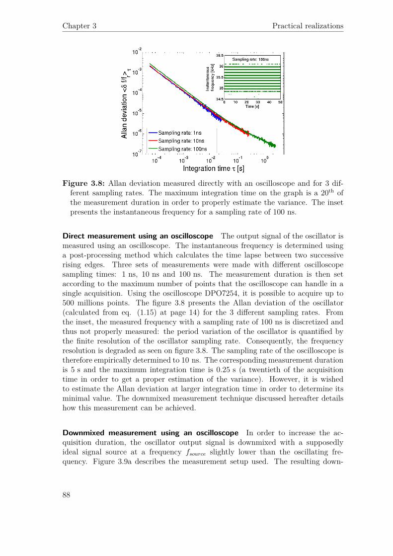
Chapter 3 Practical realizations
Figure 3.8: Allan deviation measured directly with an oscilloscope and for 3 dif-ferent sampling rates. The maximum integration time on the graph is a 20th ofthe measurement duration in order to properly estimate the variance. The insetpresents the instantaneous frequency for a sampling rate of 100 ns.
Direct measurement using an oscilloscope The output signal of the oscillator ismeasured using an oscilloscope. The instantaneous frequency is determined usinga post-processing method which calculates the time lapse between two successiverising edges. Three sets of measurements were made with different oscilloscopesampling times: 1 ns, 10 ns and 100 ns. The measurement duration is then setaccording to the maximum number of points that the oscilloscope can handle in asingle acquisition. Using the oscilloscope DPO7254, it is possible to acquire up to500 millions points. The figure 3.8 presents the Allan deviation of the oscillator(calculated from eq. (1.15) at page 14) for the 3 different sampling rates. Fromthe inset, the measured frequency with a sampling rate of 100 ns is discretized andthus not properly measured: the period variation of the oscillator is quantified bythe finite resolution of the oscillator sampling rate. Consequently, the frequencyresolution is degraded as seen on figure 3.8. The sampling rate of the oscilloscope istherefore empirically determined to 10 ns. The corresponding measurement durationis 5 s and the maximum integration time is 0.25 s (a twentieth of the acquisitiontime in order to get a proper estimation of the variance). However, it is wishedto estimate the Allan deviation at larger integration time in order to determine itsminimal value. The downmixed measurement technique discussed hereafter detailshow this measurement can be achieved.
Downmixed measurement using an oscilloscope In order to increase the ac-quisition duration, the oscillator output signal is downmixed with a supposedlyideal signal source at a frequency fsource slightly lower than the oscillating fre-quency. Figure 3.9a describes the measurement setup used. The resulting down-
88

3.1 Self-oscillating loops using discrete electronics
80,000 000 0 MHz
!"#$%&'())*+%,$-%&'$.$/01/$234
5!6$7809
//80:;$*<()=>+$&(<>*)$&%?,'=@AB$.$/0C8$234
!*&&(-$DE$F!B$GH0::34
-!"#:34 /,I$%,I=,$-'./::34
JD0K:$FL;
-MN::34
(a)
10−2
100
102
10−7
10−6
10−5
Integration time τ [s]
Alla
n d
evia
tio
n <
δ f
/fr>
τ
(b)
Figure 3.9: (a) Schematic of the Allan deviation measurement using a down-mixingarchitecture, (b) plot of the Allan deviation versus the integration time.
mixed signal is composed of two frequencies: one at low frequency |fosc ≠ fsource|and one at high frequency fosc + fsource ¥ 2fosc. Using low-pass filters, it is pos-sible to measure |fosc ≠ fsource| with a high accuracy. It can be shown that with|fosc ≠ fsource| ¥ 100 Hz and fosc ¥ 36 kHz, a 4th order low-pass filter must beemployed in order to correctly filter the high frequency term.
Because the downmixed signal is at a lower frequency, the sampling rate of the os-cilloscope can be reduced and thus one can acquire larger measurement durations:the counter part of this technique is that low integration times cannot be exploredunlike the direct measurement method. The corresponding Allan variation is de-picted in figure 3.9b and shows an Allan minimum deviation around 4.0◊10≠7 for anintegration time of 3.2 s. At higher integration times, the Allan deviation increaseswith a slope close to 1 (fitted to 0.94) what seems to correspond to a frequency drift.
Measurement with a frequency counter The frequency resolution of an oscillatorcan also be evaluated using a dedicated equipment such as a frequency counter.The frequency counter measures the number of rising edge during a given gate timeand then calculates the corresponding mean frequency. This equipment however issubject to several limitations.
First, due to the low communication rate of the GPIB connection with computer, thegate time cannot be smaller than 0.1 s. Moreover, the GPIB connection, introducessome dead time during which the frequency in not measured. From [Barnes 1990],the dead time emphasizes the effect of the frequency drift and thus imposes a con-straint on the gate time. Finally, the frequency measurement algorithm2 used bythe frequency counter seems to be sensitive to the frequency drift since the Allandeviation varies with the gate time and integration time (fig. 3.10).
2Agilent refuses to provide information about this algorithm.
89

Chapter 3 Practical realizations
10−1
100
101
102
10−7
10−6
10−5
10−4
Integration time τ [s]
Alla
n d
evia
tion <
δ f/f
r>τ
Gate time: 0.1s
Gate time: 0.2s
Gate time: 0.5s
Gate time: 1s
Gate time: 1.5s
Gate time: 2s
Gate time: 3s
Figure 3.10: Allan deviation measured with a frequency counter.
The frequency counter however provides reasonable frequency resolution measure-ment with a minimum of 4.4 ◊ 10≠7 for an integration time of 5 s and a gate timeof 1 s. This result is quite consistent with the one obtained with the downmixedtechnique.
Delay-shift based measurement This measurement is based on the techniquedescribed in section 1.4.2 and is depicted in figure 3.11a. It provides a minimalfrequency resolution of 3.9◊10≠7 ( for an integration time of 2.4 s. Once again, thisresult is consistent with the previous ones.
PZE oscillator
!"#$%&'()*+,'-./
()'01,'-"23456'789%5:5&;
<756'='>,-?@'='>,3ABA?@'='>,,3AB
<756'='>-?@'='1,3AB
+ .8900 + 120.0 1.200
(a)
10−1
100
101
10−7
10−6
Integration time τ [s]
Alla
n d
evia
tio
n <
δ f
/fr>
τ
(b)
Figure 3.11: (a) Schematic of the phase-shift based measurement, (b) evolution ofthe Allan deviation versus the integration time.
90

3.1 Self-oscillating loops using discrete electronics
10−2
10−1
100
101
102
10−8
10−7
10−6
10−5
10−4
Integration time τ [s]
Alla
n d
evia
tion <
δ f/f
r>τ
Direct measurement
Downmixed meas.
Freq. counter meas.
Phase−shift meas.
FLL on bridge+LNA
FLL on open−loop
Figure 3.12: Comparison of the Allan deviation of the SOL- and FLL-architecture.
3.1.1.5 Frequency resolution comparison of the SOL with FLL3
The frequency resolution measured with a self-oscillating loop is compared with theone obtained with a frequency locked-loop implemented with laboratory equipments,externally controlled via a GPIB communication link and a Labview interface (notthat the same microcantilever is used in all measurements). First, the frequencyresolution of the FLL was measured only with the bridge implementation and witha single commercial amplifier. As in the SOL, the amplifier is connected as closeas possible to the MEMS in order to minimize the MEMS-to-electronics connectionlosses. In a second measurement, the frequency resolution of the FLL is evaluatedon the complete open-loop scheme of the SOL architecture, including the passivefilters, the clamping amplifier and the supplementary amplifiers (the loop is openedbetween the second ADA4817-amplifier and the third one). The GPIB communi-cation between the lock-in amplifier, the computer and the VCO introduces somedelays in the loop and thus limits the minimum integration time to about 1.5 s. Thefrequency resolutions measured with the FLL-architecture and the SOL-architectureare depicted in figure 3.12. One can see that the minimum frequency resolution usinga FLL-architecture corresponds to the minimum integration time. The correspond-ing frequency resolution is about 8 times lower than the one of a SOL-architecture.
From the cantilever mass mP ZE ¥ 25 ng and equation (1.12) of page 13, the massresolutions are about ‡m≠SOL ¥ 9.8 fg for the SOL-implementation and ‡m≠F F L ¥1.3 fg for the FLL-implementation. These mass resolutions are not as good as otherNEMS-based examples in the literature due to the large dimensions of the cantilever,and because the measurements were made at ambient pressure. From [Ivaldi 2011b],the theoretical gas resolution for the DMMP is around 660 ppb.
3This work was performed with the help of Paul Ivaldi
91

Chapter 3 Practical realizations
Parameter Value
Beam’s length L = 5 µmBeam’s width b = 300 nm
Beam’s thickness h = 160 nmGauge’s length Lg = 500 nmGauge’s width bg = 80 nm
Electrode- beam gap g = 200 nm
Table 3.1: Dimensions of the cross-beam.
Figure 3.13: Image of the cross-beam. In blue, the actuation elec-trodes; in yellow, the beam and ingreen, the piezoresistive gauges.
It is believed that the SOL-architecture introduces a larger frequency noise dueto the large feed-through out of the resonance frequency: at low-frequency, thewhite and flicker noises are amplified by the feed-through transmission and are thenup-converted close to the oscillation frequency by the nonlinearity present in theloop. However, more experimental measurements and simulations are required toconfirm this possible explanation. A V-shape feed-through is difficult to model ina time-dependent simulation. A measurement setup enabling to adjust a V-shapefeed-through level would be a way to further study this topic.
3.1.1.6 Conclusion on the piezoelectric cantilever based self-oscillating loop
It was shown that using a bridge architecture and with careful filtering, it is pos-sible to implement a piezoelectric micro-cantilever in a self-oscillating loop. Aftercomparing the pros and cons of different frequency resolution measurements, it wasshown that the piezoelectric cantilever implemented in a self-oscillating loop has afrequency resolution around 4 ◊ 10≠7.
Using a FLL-architecture on a similar piezoelectric cantilever but with different di-mensions4, Ivaldi [Ivaldi 2011b] measured frequency resolution close to 10≠8 makingit an interesting gas sensor with concentration resolutions close to 10 ppb for DMMPvapors [Ivaldi 2011a]. Although the frequency resolution of the SOL-architecture isdegraded compared to a FLL-architecture, it can be an interesting low-cost alterna-tive to the expensive components required to implement the FLL-architecture.
3.1.2 Self-oscillating loop with a piezoresistive crossbeam
In this subsection, a piezoresistive crossbeam and its electrical connections are firstdescribed. The open-loop characterizations are then presented. The frequency res-
4We did not have access to these components because the number of functional devices waslimited.
92

3.1 Self-oscillating loops using discrete electronics
!"#$%$&'()*%+)%$",
-'.)%$&'()*%+)%$",
-'.)%$&'(.)+.'
!"#$%$&'(.)+.'
/')0
(a) (b)
Figure 3.14: (a) Optical image of the electrical connections of the crossbeam,(b) simulated on-chip parasitic feed-through and connection loss (the gain wasnormalized to the voltage at the resonator if no capacitance is present at theoutput of the resonator).
olution of the closed-loop system is presented in subsection 3.1.2.3 and comparedto its theoretical value determined in chapter 2. Finally, the response time of theoscillator is evaluated.
3.1.2.1 Crossbeam presentation
The crossbeam characterized in this subsection has the dimensions given in table3.1. The figure 3.13 depicts a scanning electron microscope image of such resonator.The theoretical resonance frequency is 21 MHz.
The crossbeam is designed for gas sensing applications5. The packaging and the on-chip electrical connections of the resonators were designed accordingly: the cross-beam is distanced from the electrical pads of about 2 mm so that the resonatorcan be encapsulated with ease [Li 2010, Arcamone 2011]. The figure 3.14a presentsthe electrical leads to the resonator captured with an optical microscope. As aconsequence, large connection losses between the resonator and the first electronicamplification stage are induced. Moreover, due to the geometrical configuration ofthe electrical leads, the feed-through should increase drastically. Electromagneticsimulations6 of the on-chip electrical environment were performed and are depictedon figure 3.14b. An error of 0.3 dB and 4° was introduced in the differential ac-tuation that corresponds to the typical imperfection of the hybrid coupler (PulsarJF-03-412).
With the typical parameters used in section 2.4, the expected signal-to-background
5However we have characterized the device in vacuum for future mass spectrometry applications.6performed by Gérard Billot and Jean-Baptiste David
93

Chapter 3 Practical realizations
!
!
"
#
#
#
$
$
"#$%&
(a)
18.19 18.195 18.2 18.205 18.21 18.215 18.220
20
40
60
80
100
Frequency [MHz]
Voltage n
ois
e [nV
/√H
z]
Thermomechanical noise
Measurement
Fit
Sthermo
=(63 nV/√Hz)2
Sbackground
=(28 nV/√Hz)2
Q=6 700fr=18.2 MHz
(b)
Figure 3.15: (a) Measurement setups 1 in magenta, 2 in blue, 3 in green and 4 inred. (b) Noise spectrum at the first electronic amplifier output.
ratio using a single-sided actuation is around GSBR = 7 dB, ∆ÂSBR = 48° andaround GSBR = 30 dB, ∆ÂSBR = 180° using a differential actuation. A differentialactuation is therefore required in order to simplify the implementation of the self-oscillating but also to optimize the frequency resolution.
3.1.2.2 Open-loop characterization
We have measured the following parameters of the crossbeam resonator and thefirst amplifier: the electronics gain and induced noise, the connection losses and thegauge factor.
In order to measure the electronic gain and induced noise, a network analyzer(HP8753E) and a spectrum analyzer (N9020A) connected to the amplifier wereused (as depicted in magenta and blue on fig. 3.15a): Gamp = 14 dB and Selec =16.4 nV/
ÔHz
22around 18 MHz. The datasheet of the amplifier announces a voltage
noise of 4 nV/Ô
Hz. The amount of measured noise is acceptable since the resistanceof the circuit (required to adjust the amplifier gain) introduces extra voltage noise.
In order to evaluate the connection losses, one can connect the first port of thenetwork analyzer to a gauge of the crossbeam (the second gauge is kept unconnected)and the second port to the output of the electronic circuit (in green on fig. 3.15a).From the gain of the electronic circuit and the value of the resistance of the gauge,it is possible to determine the capacitance at the output of the crossbeam: Cconnec +Celec = 30 pF. The measured value of Cconnec + Celec is reasonable as the on-chipcrossbeam output capacitance is estimated to be around 20 pF and the connectioncapacitance introduced by the SMA-connectors between the MEMS-chip and theamplifier is around 5 ≠ 10 pF . Overall, the MEMS-to-electronics connection losses
94

3.1 Self-oscillating loops using discrete electronics
−40 −30 −20 −10 0 10 20 30 40−45
−40
−35
−30
−25
−20
−15
Normalized frequency [kHz]
Tra
nsm
issio
n g
ain
S21 [
dB
]
Crossbeam with the amplifier in the chambersignal−to−background
ratio: 3dB
Crossbeam alone in the chambersignal−to−background ratio: 0.2dB
Crossbeam with the amplifierin the chamber and attenuatorsafter the hybrid couplersignal−to−background ratio >30dB
Figure 3.16: Differentially actuated crossbeam frequency response for differentmeasurement setups. NB: however that the applied voltage slightly differs betweeneach measurement setups.
can then be evaluated to: |Hconnec| = 1/ |1 + j2fifrZMEMSCoutput| = ≠21 dB.
In order to measure the gauge factor and the thermomechanical noise of the cross-beam, the gauges are polarized with a DC voltage of 3 V and the actuation elec-trodes are grounded (in red on fig. 3.15a). The spectrum of the electronic outputis recorded with the spectrum analyzer (fig. 3.15b). The thermomechanical noise isclearly observed: Sthermo = 63 nV/
ÔHz (measured at the output of the amplifier).
From this value, the gauge factor of the silicon was extracted: “Si = 77 [He 2006].
It has been observed that there is a large capacitive coupling in-between the cablesthat link the resonator in the vacuum chamber and its readout electronics: thetransmission gain is around ≠40 dB at 20 MHz. The resonance of the crossbeamis therefore difficult to observe and embedding an amplifier inside the chamber toreduce connection losses and the coupling in-between the cables is necessary (fig.3.17 and 3.16). In addition to this issue, some imperfections in the hybrid couplerused to create a differential actuation were detected. This issue can however bereduced by implementing two attenuators at the output of the hybrid coupler toadjust the phase-shift and attenuation induced by the passive device.
Figure 3.16 shows that the gain and the phase-shift of the system have to be adjustedto ensure the resonator’s self-oscillation. Using a similar electronic circuitry thanin subsection 3.1.1 (fig. 3.17), the gain of the open-loop is larger than 0 dB. AnAD8037 clamping amplifier sets a finite adjustable limit to the oscillation amplitude.The phase-shift in the loop is adjusted with a delay line rather than with filtering.The delay line is implemented using a coaxial cable with a length of about 2 meters.The figure 3.18 presents the open-loop gain and phase-shift of the system: theoscillation conditions are fulfilled only at fr.
95

Chapter 3 Practical realizations
!"#$
%&'%&'
&(
!)&(
*+,-
"*
.+.")!/
,0123451234.+)&67
859:.;<!&&
+=01>50?@=5A=10?B=#C?DE5825FG1H?105F1I0=
-!
$JKK=ALM.")8&
-!
$JKK=ALM.")8&
N?0?FG@FE?3
L@OFE?331DEP
*1FJJ2FE12I=A
,1I0=P5?@FE12I=A
!"#$%#&'()"#*+,%-.+&)/#0*%"#/#&-
*Q-
6* ROI?1P ROI?1P
[email protected]=@J1DGA
S>IA?#FGJ30=A
O%* %*
Figure 3.17: Simplified schematic of the closed-loop.
105
106
107
108
109
−60
−50
−40
−30
−20
−10
0
10
Frequency [Hz]
Op
en−
loo
p g
ain
[d
B]
−30
−20
−10
0
10
Op
en−
loo
p g
ain
[d
B]
18.4 18.42 18.44 18.46 18.48 18.5−100
−50
0
50
100
Frequency [MHz]Op
en
−lo
op
ph
ase
−sh
ift
[°]
Resonance frequency@ 18.45 MHz
Figure 3.18: Open-loop transfer function versus frequency
96

3.1 Self-oscillating loops using discrete electronics
100
101
102
103
104
105
106
−100
−80
−60
−40
−20
0
20
Offset frequency [Hz]
Ph
ase
no
ise
[d
Bc/H
z]
10−5
10−4
10−3
10−2
10−1
10−7
10−6
10−5
10−4
10−3
10−2
Integration time [s]
Alla
n d
evia
tio
n
From open−loopmeasurement ofsection 3.1.2.2
E5052A phase−noisemeasurement
From E5052A phase−
noise measurement
Temporal measurementwith edge crossing
post−traitement
Temporal measurementwith PLL post−traitement
FLL−architecture withanother crossbeam
Figure 3.19: Phase noise spectrum and Allan-deviation of the oscillator.
3.1.2.3 Frequency resolution measurement
The frequency stability of the closed-loop oscillator is measured with two differenttechniques: a spectral acquisition and a temporal acquisition. In the first acquisition,the oscillator signal is measured with an E5052A signal source analyzer. The Phase-noise spectrum depicted on figure 3.19 is then converted into its equivalent Allandeviation through the equations (1.17) and (1.30) of pages 14 and 22. Note thatthis measurement was not possible with the piezoelectric cantilever because thesignal source analyzer frequency range starts from 10 MHz. Moreover, the phase-shift based measurement used in the previous subsection is difficult to implementbecause the cables introduce large phase-shifts at this frequency: the phase-shiftvariations are thus difficult to calibrate.
The temporal acquisition uses a DPO7254 oscilloscope as discussed previously insubsection 3.1.1.4. The instantaneous frequency is extracted from the time lapsebetween two consecutive rising edges. The Allan deviation is then calculated byaveraging these instantaneous frequencies as for the piezoelectric cantilever (fig.3.19). This simple signal processing shows a large error in the evaluation of theAllan-deviation. The error is believed to be due to the poor oscillator signal-to-noise ratio at the bandwidth of the loop (what was not the case for the piezoelectriccantilever). In order to extract more accurately the frequency resolution of the oscil-lator, a digital PLL-based post-processing of the oscilloscope signal is implemented(fig. 3.19). With this post-processing technique, the temporal measurement corre-sponds to the frequency measurement. It should be emphasize that this so-calleddigital PLL processing used to evaluate the frequency resolution is different fromthe one described in subsection 1.4.3. Indeed, the data acquisition is made withthe oscilloscope (equivalent to an 8-bit Analog-to-Digital Converter) and the digital
97

Chapter 3 Practical realizations
PLL processing is made at a software level coded in C-language. Therefore, there isno need of hardware equipment such as a VCO and a phase-comparator. The Siliconarea consumption to implement this post-processing technique should therefore besmall.
It was also attempted to measure the frequency resolution of the oscillator using afrequency counter but the results were similar to the temporal acquisition using therising edge-based post-processing. It therefore seems that the algorithm used in theapparatus is based on the transition times of the signal and thus does not evaluateproperly the frequency resolution of the loop.
It clearly appears on the Phase-noise spectrum, that for low offset frequency, theoscillator noise spectrum is dominated by flicker noise. However the origin of thisflicker noise remains unclear and is under investigation.
The best frequency resolution of the resonator is around 2 ◊ 10≠7 at Tmeas = 20 ms.With the dimensions of the resonator, the corresponding mass resolution is ‡m =110 zg. The model presented in section 2.4 however predicts a mass resolutionaround ‡m≠th = 1 zg at Tmeas≠th = 1 s (considering the crossbeam dimensions, thequality factor and the actuation DC voltage used in the measurement). The dif-ference in mass resolution is due to the large flicker noise in the oscillating loop.However, it should be recognized that the mass resolution of this 18 MHz cross-beam is comparable with the state-of-the-art mass resolution of NEMS embeddedin self-oscillating loops which is ‡m≠Feng2008 = 50 zg at Tmeas≠Feng2008 = 200 ms[Feng 2008]7 . The mass resolution of the presented self-oscillation loop is thereforetwice larger than the state-of-the-art, but with an integration time 10-times smaller(larger measurement bandwidth).
3.1.2.4 Response time of the oscillator
When MEMS resonators are electrostatically actuated, a simple method to assessthe time response of a sensor is to modify the DC-actuation voltage. Indeed, theDC voltage slightly shifts the resonance frequency of the resonator through the well-known “spring-softening” effect. The response time of the oscillator can be evaluatedfrom the transition time between one DC voltage to another. The DC voltage sourcethat polarizes the actuation electrodes was replaced by a FG120 pulse generator ata frequency of 274 Hz8. The oscillator output signal is acquired with the DPO7254oscilloscope and the signal was processed with the digital PLL algorithm discussedhere-above. The evolution of the oscillation frequency versus time is depicted onfigure 3.20. The signal is fitted using an exponential time response and it is evaluatedthat the oscillator time response is below 100 µs.
7Unfortunately, the mass resolution corresponding to an integration time of 20 ms is not given inthis paper.
8An arbitrary frequency was chosen that would not be miss-confused with the harmonics of the50 Hz-frequency of the domestic supply and whose period would be close to the time responseof the sensor.
98

3.1 Self-oscillating loops using discrete electronics
0 2 4 6 8 1018.13
18.14
18.15
18.16
18.17
18.18
18.19
18.2
Time [ms]
Oscill
ation fre
quency [M
Hz]
0 2 4 6 8 10
4
4.5
5
5.5
6
6.5
7
Pola
rization v
oltage [V
]
Actuation polarization
Oscillation frequency
Fit
Time response at 18.134MHz = 120 µsTime response at 18.18MHz = 85 µs
Figure 3.20: Evolution of the oscillation frequency versus time when the DC-actuation electrodes are polarized with a pulse generator.
Such a 18 MHz crossbeam implemented in a self-oscillating loop architecture cantherefore be used to sense mass changes with sub-milliseconds sampling rates. How-ever at such a low integration time, the mass resolution is deteriorated to about5 ag.
3.1.2.5 Conclusion of crossbeam based self-oscillating loop with discreteelectronics
In this subsection, inherent difficulties with stand-alone nano-resonators were ana-lyzed and circumvented in order to implement them in self-oscillation. The on-chipfeed-through was reduced using differential actuation; the parasitic coupling in thevacuum chamber cables was reduced by introducing an amplifier in the chamber.Finally, the imperfections of the hybrid coupler were reduced using two attenuators.
The gain and noise characteristics of the 18 MHz crossbeam were measured andcorrespond to the values in the literature. Finally, we have shown that the open-loop gain and phase-shift of the resonator and its feedback circuit can be adjustedso that the system oscillates only at fr.
The frequency resolution of the oscillator was then measured using a frequency anda temporal acquisition. The two acquisition methods presented similar results if aPLL-algorithm is used to analyze the temporal acquisition. From the phase-noisemeasurement of the oscillator, it was shown that the noise spectrum is dominatedby flicker noise but its origin remains unclear at this stage.
Finally, the time response of the sensor was evaluated. The corresponding time re-sponse was measured to Tmeas = 85 µs allowing to use the crossbeam self-oscillatingloop as a mass sensor with sampling rates below millisecond.
99

Chapter 3 Practical realizations
Resonator Piezoelectric cantilever Piezoresistive crossbeam
Beam’s mass 25 ng 560 fgResonant frequency 36 kHz 18 MHz
Frequency resolution 4 ◊ 10≠7 2 ◊ 10≠7
Mass resolution 9.8 fg 100 zgIntegration time 3 ≠ 5 s 20 msGas resolution for DMMP 660 ppb 910 ppb for Qair = 150
Table 3.2: Comparison between the different self-oscillated resonators.
3.1.3 Conclusion of self-oscillating loops using discreteelectronics
Two self-oscillating loops were realized with discrete electronics: the first one in-volves a big MEMS resonator which has interesting gas resolutions. The challengeencountered during the design of the loop was to filter the V-shape feed-throughin order to prevent parasitic oscillations. The frequency resolution of the loop wasevaluated with different measurement techniques that have consistent results. Theoverall frequency resolution of the SOL-architecture is however degraded comparedto the MEMS resonator embedded in a FLL-architecture.
The second self-oscillating loop uses a 18 MHz piezoresistive crossbeam. The majortask in the implementation was to design a homodyne setup measurement thatwould reduce the feed-through signal. The frequency resolution of the resonatorwas acquired with other measurement techniques then the 36 kHz-SOL since thecrossbeam resonance frequency is much higher. With with such dimensions, thecrossbeam presents an excellent mass resolution that is comparable with the state-of-the-art.
Table 3.2 compares the performances of these two different self-oscillating loops:their relative frequency resolutions of each oscillator are similar. However withits small dimensions, the crossbeam can sense excellent mass resolution. On theother hand, the piezoelectric cantilever is interesting for gas measurement wherebya resolution of 660 ppb for DMMP vapors can be achieved. Note however that thecrossbeam resonator presents also interesting resolution for gas sensing (the oscillatorunder atmospheric pressure has however not been realized yet).
3.2 Integrated circuit for multiple crossbeams
3.2.1 Objective of the integrated circuit
The oscillators realized in the previous section use commercial electronics that areconnected to the stand-alone resonator through coaxial cables. This approach is
100
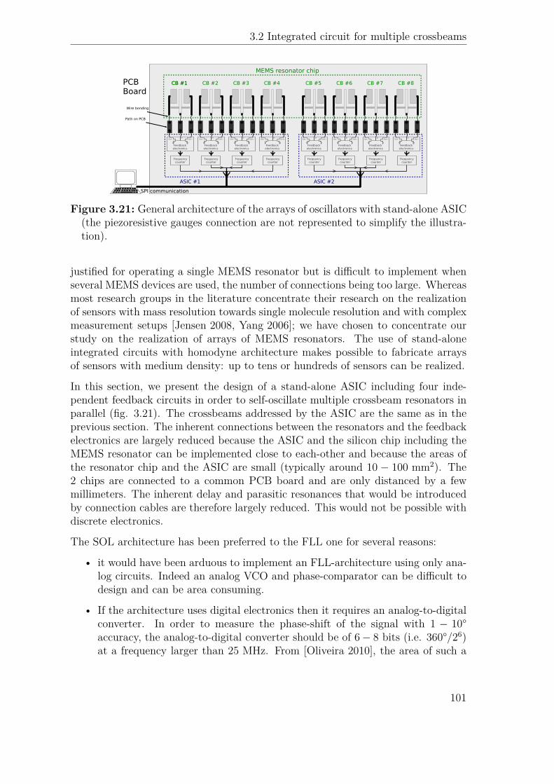
3.2 Integrated circuit for multiple crossbeams
!""#$%&'(")"&*+,-.&/
0-12*312*4
!""#$%&'(")"&*+,-.&/
0-12*312*4
!""#$%&'(")"&*+,-.&/
0-12*312*4
!""#$%&'(")"&*+,-.&/
0-12*312*4
!+"52"-&6&,2-*"+
!+"52"-&6&,2-*"+
!+"52"-&6&,2-*"+
!+"52"-&6&,2-*"+
!""#$%&'(")"&*+,-.&/
0-12*312*4
!""#$%&'(")"&*+,-.&/
0-12*312*4
!""#$%&'(")"&*+,-.&/
0-12*312*4
!""#$%&'(")"&*+,-.&/
0-12*312*4
!+"52"-&6&,2-*"+
!+"52"-&6&,2-*"+
!+"52"-&6&,2-*"+
!+"52"-&6&,2-*"+
7809(:; 7809(:<
9=(:; 9=(:< 9=(:>9=(:; 9=(:? 9=(:@ 9=(:A 9=(:B 9=(:C
DED8(+"/,-%*,+(&F.G
H9=(=,%+#
8H0(&,II2-.&%*.,-
J.+"($,-#.-K
H%*F(,-(H9=
Figure 3.21: General architecture of the arrays of oscillators with stand-alone ASIC(the piezoresistive gauges connection are not represented to simplify the illustra-tion).
justified for operating a single MEMS resonator but is difficult to implement whenseveral MEMS devices are used, the number of connections being too large. Whereasmost research groups in the literature concentrate their research on the realizationof sensors with mass resolution towards single molecule resolution and with complexmeasurement setups [Jensen 2008, Yang 2006]; we have chosen to concentrate ourstudy on the realization of arrays of MEMS resonators. The use of stand-aloneintegrated circuits with homodyne architecture makes possible to fabricate arraysof sensors with medium density: up to tens or hundreds of sensors can be realized.
In this section, we present the design of a stand-alone ASIC including four inde-pendent feedback circuits in order to self-oscillate multiple crossbeam resonators inparallel (fig. 3.21). The crossbeams addressed by the ASIC are the same as in theprevious section. The inherent connections between the resonators and the feedbackelectronics are largely reduced because the ASIC and the silicon chip including theMEMS resonator can be implemented close to each-other and because the areas ofthe resonator chip and the ASIC are small (typically around 10 ≠ 100 mm2). The2 chips are connected to a common PCB board and are only distanced by a fewmillimeters. The inherent delay and parasitic resonances that would be introducedby connection cables are therefore largely reduced. This would not be possible withdiscrete electronics.
The SOL architecture has been preferred to the FLL one for several reasons:
• it would have been arduous to implement an FLL-architecture using only ana-log circuits. Indeed an analog VCO and phase-comparator can be difficult todesign and can be area consuming.
• If the architecture uses digital electronics then it requires an analog-to-digitalconverter. In order to measure the phase-shift of the signal with 1 ≠ 10°accuracy, the analog-to-digital converter should be of 6 ≠ 8 bits (i.e. 360°/26)at a frequency larger than 25 MHz. From [Oliveira 2010], the area of such a
101

Chapter 3 Practical realizations
circuit would be of 0.12 mm2 minimum. It will be shown that this area is largecompared to the overall circuit.
• It can be argued that a downmixing architecture (see subsection 2.3.3) can beemployed in order to reduce the constraints on the analog-to-digital converterbecause the sampling frequency is reduced. However, this architecture wouldimpose large constraints on the front-end analog filtering needed before theanalog-to-digital converter.
Overall, it is believed that an FLL-architecture would be too challenging (in termsof design time and risks) to design the proposed application.
Implementing both the complete feedback electronics and a frequency counter seemsa much more compact and feasible solution. Only a clock reference, a communicationcable with a computer and a DC power are required. The packaged ASIC with anarea of 7 ◊ 7 mm2 (the actual silicon die is of 2 ◊ 2 mm2, the rest of the areais dedicated to the packaging) also offers the possibility of using several ASIC inparallel in order to address dozen or more resonators.
However, the fabrication of several resonators and feedback electronics each on asingle chip has some counterparts: some electrical and mechanical coupling mayappear between the different resonators or between the different circuits within theASIC chip. The characterization of the multi-oscillators system makes it possible toassess the coupling when electromagnetic models would probably fail at this task.
3.2.2 Global architecture
The ASIC is composed of 4 blocks containing each a feedback circuit and a frequencycounter; a power management block and a SPI communication interface so that thechip can be directly connected to an external computer (fig. 3.22). The ASICis therefore composed of analog and digital electronics. The analog signal in eachoscillating loop is converted into a digital signal and its frequency is measured in realtime via the digital frequency counter. The measured frequencies are averaged over aminimal integration time of 10 µs. The averaged oscillation frequency is then sent toa computer through the SPI communication interface. The communication protocolis also used to configure specific parameters (such as the polarization current or thecut-off frequency of the filters) of the self-oscillating circuit.
The frequency counters sampled at 1 GHz consist in counting during a fixed timeTmeas the number of rising edges of the oscillating signal. In order to achieve a largeraccuracy in the frequency measurement, the time of the first and last rising edge aremeasured and the mean frequency is modified accordingly to the method presentedin subsection 1.4.1 of page 33. From eq. (1.59) at page 33, a frequency resolutionbetter than 10≠7 is achieved for Tmeas Ø 15 ms which is compatible with the results ofsubsection 3.1.2. It should be mentioned that the frequency measurement techniqueimplemented in the ASIC provided poor resolution in subsection 3.1.2. The issue
102

3.2 Integrated circuit for multiple crossbeams
!""#$%&'(")"&*+,-.&/
0-12*312*4
!+"52"-&6&,2-*"+
!+"52"-&6&,2-*"+
!+"52"-&6&,2-*"+
!+"52"-&6&,2-*"+
7809
9:(;< 9:(;= 9:(;>9:(;< 9:(;?
@A@8(+"/,-%*,+(&B.C
D,E"+F%-%G"F"-
*
9),&'F%-%G"F"-
*
8D0&,FF2-.&%*.,-
!""#$%&'(")"&*+,-.&/
0-12*312*4
!""#$%&'(")"&*+,-.&/
0-12*312*4
!""#$%&'(")"&*+,-.&/
0-12*312*4
H.G.*%)&,-*+,)
!"
"#$%&
"$'()*+,
Figure 3.22: General architecture of the ASIC (the piezoresistive gauges connectionare not represented to simplify the illustration).
was only discovered after the design of the ASIC but we hope that including thecomparator in the loop as it is done in the ASIC can prevent this issue.
The architecture implemented in the ASIC allows to activate or deactivate eachoscillator on demand. It also offers the possibility to measure each oscillating fre-quency in parallel or sequentially. The coupling between each oscillator can thusbe evaluated: it is possible for that a frequency shift is detected on an unloadedresonator due to coupling effects with a loaded resonator.
3.2.3 General topology of the proposed oscillator
The ASIC input signal (corresponding to the resonator output signal) is first bi-ased so that the ASIC characteristics are independent of the crossbeam DC outputvoltage. The electrical signal is then amplified in order to increase its amplitudeand to neglect the noise contribution of the following stages. The following analogstages are dedicated to further amplify and to filter the signal in order to preventparasitic oscillations at other frequencies than fr. Note that the analog blocks arebiased by independent current sources whose values can be adjusted. The tunabilityof the bias current makes the ASIC more robust and the ASIC characteristics canbe modified if needed.
Because the resonator and the ASIC are fabricated on different wafers and connectedby wire bonding, it is assumed that the connections could modify the phase responseof the crossbeam’s resonance and that the phase-shift introduced by the connections
103

Chapter 3 Practical realizations
!"##$%&'"()*#+",-&
.!/
012-$3$&4
56
7
8!"##$%&9!/
0:"-;<
=$<$+"-
0>+$%&9!/
?;12"4"+;4
/'@'A
/4&BC($%$(&4
=&-"D-;>E&(8-;;2
/'F'A
/4&BC(;*,-&4
(&">+$%",-&
GHI*33&4
GH
J:%&4+&4
=$33&4&:+$"-'">+*"+$;:
K;'+L&'34&BC>;*:+&4
Figure 3.23: General architecture of the self-oscillating loop.
!"#$%&' !"#$%&()'!"#$%&*)'!"#$%)' !"#$%+'
,-./0
1+
!"#$%&'()*#+#,(+
1+( 1+*
!"#
2
-"#+.%&*/)*
0/1,2*1%3%+
!"#
34/05*04.67058597.:&
0$%)'
0$%;'
0$%<'
0$%='
0$%>'
0$%?'
1+*@58/A5@
&74$@58/A$07/B5&*)74$@58/A$07/B56.C07$@58/A$07/B5 &()74$@58/A$07/B5 +74$@58/A$07/B5
Figure 3.24: Schematic of a delay-locked loop.
would be difficult to predict accurately. The architecture of the oscillator shouldtherefore be capable to phase-shift the input signal to any value. To the author’sknowledge there is no analog architecture capable of finely tuning the phase-shift ofthe signal that is compact and low power.
Therefore, an analog/digital mixed architecture has been preferably implemented.It uses a delay lock loop (DLL) that consists of a series of delay blocks which arecontrolled by a feedback loop (fig. 3.24). Each delay block is basically an inverterand therefore the delay introduced by each block is a function of its bias current.It is then possible by adjusting the bias current to control the delay introduced byeach stage. The output of the last delay block (IN ≠ delayed) is compared to theinput signal (IN) with a phase comparator. The delay of each delay block is thencontrolled through a charge pump so that a 2fi-phase-shift is imposed between thesignal IN and the signal IN ≠delayed. The phase-shift introduced by the nth-delayblock is then 2fi ◊ n
Nwhere N is the number of delay blocks. Using a multiplexer it
104

3.2 Integrated circuit for multiple crossbeams
is then possible to select any output of the delay line and therefore select a signalwith the desired phase-shift according to the input signal. A delay line composedof 64 blocks was implemented: the phase-shift resolution of the DLL is therefore2fi/64 < 6°. Note that the DLL can also be used to compensate any phase-shiftintroduced by the rest of the feedback circuit.
Saturating the signal at the output of the analog front-end into a 1-bit signal makesit also possible to easily control the amplitude of the oscillation because it is fixedby the supply voltage. The counterpart of this approach is that the comparator,used to convert the analog signal into a 1-bit digital signal, is highly nonlinear andthus transposes the flicker noise close to the carrier (see subsection 1.3.1.4 at page25). For this reason, one should filter the flicker noise to limit this effect. The nextsubsection will discuss in more details this aspect.
Finally large 2.5 V buffers are designed to drive the crossbeam with a high actuationpower.
NB: the design of the different blocks of the ASIC was divided between the actorsof the project. I designed the analog blocks and realized their layout as well as thecomparator layout.
3.2.4 Analog circuit design
The simplified schematic of the analog part of the circuit depicted in figure 3.25 iscomposed of the following stages:
• a biasing block,
• a low-noise amplifier (LNA),
• a low-pass filter,
• an active high pass filter with a gain of 10,
• and a comparator with an adjustable offset.
Low-noise amplifier A fully differential low-noise amplifier is designed. The DCvoltage on each input transistors (M13 and M14) are imposed by the biasing blocksdescribed in the following paragraph. The AC signal to be amplified is then con-nected through a decoupling capacitance to the positive input of the amplifier. Thefully differential architecture of the amplifier makes possible to convert the inputsignal of the crossbeam into a differential signal. Several other architectures couldalso convert the MEMS output signal into a differential one but these architecturesintroduce larger noise [Palmisano 2003]. As a matter of fact, they are not suitableto low-noise and high frequency applications. The dimensions of the transistors arechosen large enough in order to achieve a low white and flicker noise at the input ofthe amplifier. However, the length of the transistor gates are designed based on the
105

Chap
ter3
Practical
realizations
!"#"$
!"#"$%&'#
(')$*++",-)./++'+
0123,&*-)4/56/,7
!"#"$%89
!"
!&'#
"!
:";"+",$")4/56
0<=> 0<=? 0<=@ 0<=A
0<=> 0<=? 0<=@ 0<=A
!012B
!012C
2DE*6-54#")#'FB&566);/#-"+
9A?
9A@
9AA
9AG
2$-/H")I/7IB&566);/#-"+
J<=C
J<=B
KL(
9'.&5+5-'+
M?
M@
MA
3?
MG
MN
MO
3@
9? 9
@
M??
M?@
M?A
M?G
M?N
M?O
M@?
M@@
M@A
M@G
M@N
M@O
M@P
M@Q
9@?
9@@
9@A
9@G
9@N
9@O
9@P
9@Q
MA?
MA@
MAA
MAG
MA?
3A?
3A?
MG?
MG@
3G?
MGA
3G@
MGG
9+'664"5.)'*-&*-
Fig
ure
3.2
5:
Sim
plifi
edsch
ematic
ofth
ean
alogcircu
it
106

3.2 Integrated circuit for multiple crossbeams
trade-off between low-flicker noise and high input capacitance. Overall the amplifierhas a typical voltage gain of 20, a bandwidth of 120 MHz and an input noise of1.5 nV/
ÔHz.
Finally, as in all fully differential amplifier, a control of the common mode is required.Two other single-ended amplifiers are implemented in order to control the commonmode. The power consumption and the capacitance at the output of the LNA arereduced by diminishing the width of the single-ended amplifiers by a factor 10.
Biasing blocks The biasing block with the input decoupling capacitance C1 makesthe electronic circuit independent of the crossbeam resonator’s DC output voltage.The biasing stage is composed of transistors with the same length than the ones ofthe LNA but with a smaller width in order to both reduce the silicon area and theinput noise. It might seem that reducing the size of the transistors increases thethermal electronic noise but in our case, the coupling capacitance filters the noiseat high frequencies (i.e. around the crossbeam resonance frequency). Indeed, thevoltage noise at the input of the LNA can be approximated to:
vnoise≠bias =
8/3kBTgm≠bias---j2πf
C1Cp
C1+Cp+ gm≠bias
---¥
8/3kBTgm≠bias
2πfC1Cp
C1+Cp
if gm≠bias π 2πfC1Cp
C1 + Cp,
(3.2)
where gm≠bias is the equivalent admittance of the biasing block and Cp the MEMS-to-electronics connection losses. The equivalent impedance of the transistors shouldbe large in order to have a good impedance matching with the resonator outputimpedance. Moreover, in order to achieve a very low noise at the LNA input (¥0.5 nV/
ÔHz), the capacitance C1 should equal to 30 pF. Another biasing block is
designed for the other input transistor of the LNA in order to bias identically theamplifier. However, the noise at lower frequencies is large but it is filtered in thefurther blocks.
The large dimensions of the transistors M13 and M14 of the LNA introduce a capac-itance between their gates and sources. A parasitic path is created between the twoinputs of the LNA and thus the AC input signal on M13 can be transferred to thegate of M14. The AC signal at the inputs of the LNA varies in phase and the gainof the amplifier vanishes. A large grounded capacitance (C2 = 15 pF) is introducedat the input of the transistor M14 in order to reduce the AC signal at M14 createdby the existing path.
Passive adjustable low-pass filter The passive first-order low-pass filter allow ad-justing the bandwidth of the LNA. By introducing a variable capacitance at the am-plifier output, the bandwidth of the LNA is modified and thus high frequency-noisecan be filtered. A set of capacitances are connected or not to the LNA output viaNMOS switches. The capacitance at the amplifier output can be adjusted through6 configuration bits.
107
Chapter 3 Practical realizations
Active high-pass filter The constraints imposed on the high-pass filter are to filterthe frequencies lower than 10 MHz while introducing little supplementary noise inthe loop. The block cannot be realized with gm ≠C filters [Sansen 2006] because thearchitecture cannot introduce little noise while respecting the impedance criteria (ahigh input impedance compared to the output impedance of the LNA, and a lowoutput impedance compared to the input impedance of the following comparator).
The proposed structure is a classic differential active first-order high-pass filter basedon a differential amplifier designed to introduce a gain close to 50. The feedbackloop is composed of a resistance (implemented with the PMOS transistors M31 andM33) and capacitance. The structure has a high pass filter behavior and introducesan overall gain close to 10.
The transistors M32 and M34 are designed to introduce a DC threshold voltagebetween the input and the output of the high-pass filter so that it reduces the size ofthe transistors M31 and M33. Moreover, this approach reduces the area consumptionand improves the reliability of the transistors M31 and M33.
Comparator with an adjustable offset The comparator uses two single-sidedbuffer with adjustable bias current. By adjusting the bias current, the saturationvoltage of the transistors M41 and M42 can be adjusted and a DC offset betweenVcomp+ and Vcomp≠ can be introduced and adjusted. The variable offset was imple-mented in the loop in order to compensate any mismatch in the previous amplifica-tion stages but also so that parasitic oscillations may be prevented. The comparatorthen consists of a classic 2-stages single-ended amplifier with an inverter at its out-put. A special care was given in the layout of such design to prevent any parasiticsignal from the inverter (i.e. the digital circuit) to propagate in the analog circuit.
3.2.5 Overall simulations and layout
Figure 3.26 depicts the ASIC layout. As announced, the die area is 2 ◊ 2 mm2.The pad ring composed of 48 pads fills a large area and the actual circuit is about1.5 ◊ 1.5 mm2. The circuit is divided between the 4 feedback circuits (with an areaof 0.29 mm2 each) and the digital circuit of control. The layout of a feedback circuitis depicted in figure 3.27. The adjustable current sources occupy the largest area,the area is then decomposed between the analog front-end and the DLL. If a secondversion of the ASIC is realized, the experience acquired from the characterizationof the first chip should allow in the future to remove the adjustable current sourcesand thus to reduce the area consumption of the chip to 0.15 mm2 or less. Moreover,with the characterization of the first chip and if the phase-shift introduced by thecrossbeam is repeatable, then the DLL might be optional.
Only the analog circuit characteristics are presented in this section because it is thecircuit that I designed. It was simulated over a range of temperature from 20° to
108

3.3 MEMS/CMOS co-integration
!"#"$$
!"#"$$
%&'"()*+
!"#$%&&
!"#$%&&
'%())*+,-.%-/0-1/23
4/5/2,6%-/0-1/27)8-)92%4::3;
<#=$%&&
<#''%&&
Figure 3.26: Layout of the ASIC.
!"#$%&'(&)*+%,-.(
!-/01'((+2&,345
6&*701'((2&,345
8-91'5'3-5
#:;<(3'%,4+.<554)3+(-<5.4(
=4,'>+,-.?+,--1
8<554)3+542454).4
!"#$%&
'"$%&
(##$%&
)"#$%&
Figure 3.27: Layout of the feedbackcircuit.
80° and over various process corners. The circuit except the comparator has thefollowing characteristics:
• the gain at 20 MHz is larger than 140,
• the bandwidth can always be larger than 100 MHz,
• the high pass cut-off frequency is in-between 6.5 MHz and 11.5 MHz
• the electronic input noise is lower than 1.8 nV/Ô
Hz.
The overall ASIC is based on a mixed analog/digital architecture whereby the ana-log front-end filters and amplifiers the signal. The mixed architecture makes thefeedback-loop very flexible and best suited to the application. Indeed, the phase-shift, the bandwidth, an offset and the biasing current of the analog stages can beadjusted in the loop. All in all, the architecture remains compact so that is canaddress multiple resonators: it is possible to implement an array with a typicaldistance of 500 µm between each resonators.
Furthermore, the flexibility introduced in the loop can be simplified in the case of asecond ASIC and thus a more compact ASIC can be realized.
3.3 MEMS/CMOS co-integration
3.3.1 Context and objectives
In the chapter 2, it was theoretically shown that integrating the MEMS on thesame wafer as the CMOS circuit reduces both the connection losses and the feed-through. Moreover, the integration of MEMS resonators with CMOS circuits isrequired to fabricate large arrays of sensors. When millions of MEMS resonatorsare implemented in arrays, the wire bonding to individually connect the resonators
109

Chapter 3 Practical realizations
!"##$%&%$'"$()*+),"(-$%
./.0
1(2)345+%$6,(7-,%+7(8+$9$)-%,(4)6:+)9,6$829,,5+./.02;.10
&$$8<7)=$9$)-%,(4)6
(a)
!"#$%&'%()
*+''() ,((-./01($(02)34%05
6768
,)(9+(40:;03+42()
<4&0=%#;)(534/23);/4-;($(02)34%05>;3#(4&$33#;6768&?6<8
(b)
Figure 3.28: General topology of the integrated resonator with the electronics: (a)fully-integrated oscillator, (b) oscillator implemented with an external feedbackelectronics.
to the sustaining electronics becomes unrealistic and too costly. The fabrication ofthe resonators and the CMOS circuitry on the same wafer is a necessary technologicalstep to realizes sensors for mass spectrometers. This thematic was investigated inthis work through three different projects:
1. In the first project, a ST-0.35µm bulk CMOS process is adapted to be compat-ible with a MEMS resonator on a SOI-wafer. The integrated MEMS resonatoris a clamped-clamped beam that uses an electrostatic actuation and a capac-itive detection. The beam and the electrodes of the MEMS are highly dopedusing a similar doping level than for the transistors contacts.
2. In the second project, a FDSOI-process developed at Leti for digital electronicsis adapted to be 2D co-integrated with piezoresistive resonators. This home-made process offers more flexibility, e.g. one can choose the type of SOI-waferand the doping level of the MEMS (and thus to use piezoresistive detection).
3. In a third project, the 3D-integration where the single-crystal MEMS resonatorlays on top of its circuity in a 3D-stack is explored. The fabrication is basedon another FDSOI-process developed at Leti for digital electronics.
In each project, the technological process of the CMOS transistors was modified tobe adapted to the MEMS resonators. It was then assumed that the characteristics ofthe transistors may vary from the models of the design kit. The electronic circuitswere designed to be flexible and simple. The on-chip systems composed of theresonator and the electronics were designed based on two different strategies: theywere either implemented in a closed-loop or an open-loop architecture as depictedin 3.28. In the closed-loop configuration (fig. 3.28a), the output of the feedback
110

3.3 MEMS/CMOS co-integration
electronics is connected to the resonator actuation voltage. The buffer thereforedrives the oscillator signal out of the Silicon chip. The buffer is designed to chargeto connection cables between the MEMS-CMOS chip and an external measurementapparatus (e.g. a frequency counter). The feedback electronics is designed so thatthe MEMS+feedback electronics respect the oscillation conditions. In the open-looparchitecture (fig. 3.28b), the oscillator is realized out of the chip by the use of anexternal feedback circuit. The on-chip open-loop architecture is more flexible andless risky because the gain and the phase-shift of the open-loop can be adjustedexternally. In this case, the amplifier is designed to provide a gain sufficient so thatthe noise of the following stages can be neglected. The reduced constaints on thedesign of the amplifier makes it possible to design such block with smaller input noisethan in the on-chip closed-loop configuration. The buffer is similar to the one of theclosed-loop configuration because the connection capacitance between the MEMS-CMOS chip and an external measurement apparatus (here a lock-in amplifier or aphase-shifter to implement a FLL or a SOL) are similar. Overall, fully-integratedoscillators are often preferred in a final product or in the domain of high densityarrays of sensors.
In the two first projects, closed-loop architecture were implemented. As mentionedpreviously, the 2D co-integration reduces in a large manner the connection losses. Itwill be shown that in the two first projects, the product gMEMS ◊ |Hconnec| is closeto 1 and thus the gain of the sustaining electronics is low. The feedback circuits canthen be based on a Pierce oscillator topology that uses only a single active transistor.A trade-off must be found regarding the dimensions of this transistor: if its area istoo large, its input capacitance is large what increases the connection losses. If itslength is small, the transistor provides low gain. If its width is too small, than thetransistor cannot charge the capacitance of the following electronic stage (i.e. thebuffer). The theoretical design of the Pierce oscillator in the case of the resonatorswith a capacitive or a resistive detection is described in the following subsection.
3.3.2 Theoretical design of a co-integrated MEMS Pierceoscillators
This subsection addresses the feasibility of a fully-integrated MEMS-based Pierceoscillator in cases when the motion of the resonator is converted into an electricalsignal through (a) capacitive or (b) resistive detection. Our approach uses a MOSBerkeley level 1 model description of a standard CMOS technology. This method-ology can easily determine for a given MEMS or NEMS resonator if it is possibleto implement it in a Pierce oscillator scheme, and can also be used as a designrule to shrink the resonator’s dimensions down to achieve the highest resonance fre-quency. As a study case, the approach is illustrated on electrostatically-actuatedresonators: (a) a clamped-clamped beam resonator using capacitive sensing, and(b) a piezoresistive crossbeam. Both oscillators are based on a STMicroelectronics
111

Chapter 3 Practical realizations
HCMOS9 design kit. The technology makes it possible to fabricate transistors withgate length dimensions as small as 130 nm making it good candidate for high fre-quency applications without the high fabrication cost and the constraints of moreadvanced processes.
3.3.2.1 Oscillation conditions
As described in section 1.3.1.1, the Barkausen conditions for a system to oscillateat fosc are:
|HMEMS (fosc) ◊ Helec (fosc)| > 1 and arg [HMEMS (fosc) ◊ Helec (fosc)] © 0 [2fi] .
(3.3)
To oscillate at fr, the electronic circuit must then have a gain at fr larger than1/gMEMS and a phase-shift Âelec equal to ≠ÂMEMS. If the electronics introduce asupplementary phase-shift ∆ so that Âelec = ≠ÂMEMS + ∆Â, and if the gain issufficient, the resonator will still oscillate at a frequency fosc little different from fr9:
fosc ¥ fr
A1 +
∆Â
2Q
B. (3.4)
By definition, the gain of the MEMS resonator at fosc is smaller than gMEMS. Itsvalue can be approximated to:
|HMEMS (fosc)| ¥ gMEMS
C1 ≠ ∆Â2
2
D. (3.5)
From equations (3.3) and (3.5) it is seen that to ensure oscillations, |Helec (fosc)|must increase as ∆ increases. A trade-off must be established in order to achieve alarge electronic gain while introducing small ∆Â. The goal of the electronic designshould then be to maximize the quantity expressed by:
|Hpselec (fosc)| = |Helec (fosc)|
A1 ≠ ∆Â2
2
B. (3.6)
3.3.2.2 Sustaining electronics for a capacitive MEMS resonator
In this subsection, we show that, for the architecture shown in fig. 3.29, thereexists optimal transistor dimensions for MA for which |Hps
elec (fosc)| is maximized.Approximate expressions of the optimal transistor width WA≠opt and length LA≠opt
are:Y__]__[
WA≠opt ¥ 3
Ú2πfrCloadC2
connec
16KÕ
nC2gd0
VE
LA≠opt ¥ (Vgs ≠ VT ) 3
Ú2KÕ
nCconnec
2πfrCloadCgd0V 2E
, (3.7)
9Obtained from a first order Taylor expansion of HMEMS
112

3.3 MEMS/CMOS co-integration
!"#$%#&'()*+*"#,'-*
.*#*"#&'()*+*"#,'-*
/*%0!"#
$!
1!
1/
%&'()
& *#+,,-.
/#0,,-.
!1'&
!"#"$%&%'()*(+,-"&,*
.%-/0()"$&%'(&*"-+%+&,*)"1#0%2%(*
!(23
4.5.6
%1
2'3%,-4)5&657&08*-%("*)9&%4&(6
3$&4"&%,-)(0($&*,5(
6(&($&%,-)(0($&*,5(
3$&4"&%,-)(0($&*,5(
6(&($&%,-)(0($&*,5(
/*%0)#5&":(*44;<=>)(0
71
%4-
%*)8
*.!"
#
*)689
#$%&
%':3
"'(')
"*+,
-.'.%
".'.%
/
0.'.%
!"1),
%.5.6
7(+,-"&,* .4+&"%-%-/)(0($&*,-%$+
Figure 3.29: Transimpedance amplifier schematic (left) and its equivalent smallsignal schematic for a capacitively sensed resonator (right).
where
• Cload = 200 fF is the Pierce oscillator output capacitance,
• K Õn = 125 µA/V2 is the transconductance coefficient,
• Cgd0 = 0.5 fF/µm nominal gate-drain capacitance,
• VE = 7.7 V/µm is the impedance parameter,
• Vgs = 0.6 V is the gate-source DC voltage,
• VT = 0.36 V is the threshold voltage.
The resulting electronic gain is:
---Hpselec≠opt (fosc)
--- ¥ 3
83
ııÙ 2K ÕnVEC3
MEMS
2fifrC2connecCloadCgd0
, (3.8)
where CMEMS is the output capacitance of the resonator. The corresponding elec-tronic supplementary phase-shift is ∆ = 0.5 rad that corresponds to an oscillatingfrequency of: fosc ¥ 1.00025 ◊ fr.
Description of the circuit Figure 3.29 shows the schematic of the capacitiveMEMS-based Pierce oscillator and its small signal equivalent circuit, where:
• gm is MA’s transconductance,
• ZP is MA’s gate biasing impedance,
• CgdA is MA’s gate-drain capacitance,
• gdsA is MA’s drain-source admittance,
• gdsB is MP ’s drain-source admittance,
• Cin = Cconnec + CgsA,
• CdbA is MA’s drain-bulk capacitance,
113

Chapter 3 Practical realizations
1 10 1002
3
4
5
6
7
8
9
10
frequency [MHz]
Ele
ctr
onic
gain
Analytical formula (2)
SPICE simulations
(a)
!"#$%#&'()
*+,-.)!"/) #$%#$% &' ! )
*01201.)
!(/) (( &' ! )
*01201.)
$)#$%*+ " )
3) 456724589) 75:2353) ;5;)
8) 456724589) 75:2353) 95;)
<) 456=24584) <5<245=) 954)
34) 458924567) 95=245:) <54)
84) 45<324539) =5=245<) 857)
<4) 459324537) 335:24576) 65;)
344) 45=324538) 3:5<2458=) 653)
) (b)
Figure 3.30: (a) Comparison between the analytical formula (9) and SPICE sim-ulations, (b) transistors dimensions
• CdbB is MB’s drain-bulk capacitance,
• Cout = Cload + CdbA + CdbB.
The small signal equivalent schematic of the circuit uses the Berkeley level 1 [Sansen 2006]model of the transistors. The electronic design of the Pierce-oscillator consists indetermining the optimal dimensions of the transistors MA and MP . Their dimen-sions determine the values of gm , CgsA, CgdA , gdsA , ggsP , CdbA , CdbP and thereforethe amplification capability of the electronics. Note that it is considered that theMEMS resonator output capacitance CMEMS is negligible compared Cconnec (that istypically in the order to 5 fF).
The resonator output voltage vMEMS is attenuated due to the connection losses andthe resulting voltage is velec. The active transistor MA amplifies and converts velec
into a current which is then converted back into a voltage through Cout. If the effectsof CgdA, gdsA, ggsP and ZP are negligible, the electronic circuit has the following idealtransfer function at a frequency fosc:
H idealelec =
vout
vMEMS
=≠gmCMEMS
j2fifoscCinCout
¥ ≠gmCMEMS
j2fifoscCpCload
. (3.9)
Such an ideal circuit introduces a +90 phase shift in the oscillator feedback loopand thus ensures that the oscillations conditions 3.3 can be met at f = fr. However,it is not possible in practice to achieve a large transimpedance gain (i.e. large gm
or small Cin) without increasing the values of CgdA, gdsA, ggsP and ZP . The nextsub-section is devoted to the determination of an optimal design of the electronics.
114

3.3 MEMS/CMOS co-integration
Maximum electronic gain The non-ideal electronic transfer function has the fol-lowing expression:
Helec = ≠j2fifoscCMEMS (gm ≠ j2fifoscCgdA) /;
gdsA + gdsP
ZP
+
j2fifosc
5(gdsA + gdsP ) (CMEMS + Cin + CgdA) +
Cout + CgdA
ZP
+ gmCgdA
6≠
≠ (2fifosc)2
Ë(CMEMS + Cin + CgdA) (Cout + CgsA) ≠ C2
gdA
ÈÔ. (3.10)
We assume that:
• the MEMS resonator output capacitance is negligible compared to Cp: CMEMS πCp < Cin,
• the effect of MP can be neglected (i.e. gdsP π gdsA, CdbP π Cload),
• the effect of MA biasing can be neglected (i.e. ZP ∫ 12πfoscCout
, ZP ∫Cout
Cin
1gdsA+gdsP
),
• the transistors dimensions respect 50 nm π LA π 50 µm and WALA π15000 µm2 so that CgdA π CgsA, CdbA π Cload, gm ∫ 2fifoscCgdA,
• the gate-source capacitance of MA is low compared to the shunt capacitance:CgsA π Cp.
With the previous consideration, the expression of the electronic transfer functionHelec can be written as:
Helec = H idealelec
1
1 ≠ H idealelec
1CdgA
CMEMS+ gdsA
gm
Cp
CMEMS
2 . (3.11)
The phase introduced by this circuit is Âelec = fi/2+arctanË---H ideal
elec
---1
CdgA
CMEMS+ gdsA
gm
Cp
CMEMS
2È
and its gain is |Helec| = H idealelec /
Ú1 +
---H idealelec
---2 1
CdgA
CMEMS+ gdsA
gm
Cp
CMEMS
22. Assuming
∆ = Âelec ≠ fi/2 is small, a Taylor expansion of (3.11) yields:
|Helec| ¥---H ideal
elec
--- ◊11 ≠ ∆Â2/2
2. (3.12)
In other words, ∆ not only introduces a resonator gain reduction (cf. eq. (3.5)) butalso a circuit gain reduction. A modified gain (|Hps
elec| = H idealelec ◊ (1 ≠ ∆Â2)) takes
into account the resonator gain reduction due to ∆ can be introduced. Startingfrom the Berkeley level 1 model [Sansen 2006] applied to the transistor MA:
gm = 2K Õn
WA
LA
(Vgs ≠ VT ) , gds =K Õ
n
VE
WA
L2A
(Vgs ≠ VT )2 , Cgd = Cgd0WA, (3.13)
115

Chapter 3 Practical realizations
where WA, LA are the width and length of MA, respectively. The expression of|Hps
elec| can then be expressed in terms of WA and LA:
|Hpselec| =
2K Õn
WA
LA(Vgs ≠ VT ) CMEMS
2fifoscCpCload
◊SU1 ≠
2K Õn
WA
LA(Vgs ≠ VT )
2fifoscCpCload
3Cgd0W + Cp
Vgs ≠ VT
2LVE
4TV . (3.14)
Maximizing |Hpselec| with respect to WA and LA yields to the following expression of
the optimal parameters WA≠opt, LA≠opt and---Hps
elec≠opt
---:
Y______]______[
WA≠opt = 3
Ú2πfoscCloadC2
connec
16KÕ
nC2gd0
VE
LA≠opt = (Vgs ≠ VT ) 3
Ú2KÕ
nCconnec
2πfoscCloadCgd0V 2E---Hps
elec≠opt
--- = 38
3
Ú2KÕ
nVEC3MEMS
2πfoscC2connecCloadCgd0
. (3.15)
As---Hps
elec≠opt
--- depends on CMEMS and thus on the characteristics of the resonator, it
is possible to introduce the transimpedance gain of the circuit defined as Y pselec≠opt =
vout
iMEMS, where iMEMS is the output current of the resonator. The evolution of---Y ps
elec≠opt
--- is depicted in figure 3.30a. SPICE simulations performed with the HC-
MOS9 design kit from STMicroelectronics confirm the numerical value of---Y ps
elec≠opt
---
and thus of---Hps
elec≠opt
--- as given by (3.15) (note that the transistors dimensions are
different for each fr and therefore for each SPICE simulations as given in (3.15)).
The optimization of---Hps
elec≠opt
--- determines that ∆ is constant: ∆ = 0.5 rad. It
implies that the oscillation frequency is slightly shifted with the following value (hereQ = 1000):
fosc
fr
¥ 1.00025, (3.16)
where fosc is the oscillation frequency in the loop. The results of equation (3.15) forf = fosc are therefore also valid at fr.
Illustration: maximum oscillating frequency for a clamped-clamped beam res-onator Let us consider a capacitive clamped-clamped beam with fixed dimensions(b = 300 nm, h = 160 nm, g = 200 nm) and varying length. The fixed dimensionscorresponds to the crossbeam measured in subsection 3.1.2. Based on section 2.2.1.2fr and gMEMS have the following expressions:
fr =⁄2
2fi
ÛcSi
12flSi
b
L2, gMEMS =
12Á0÷A÷DQ
⁄4cSi
V 2DC
L4
b3g3. (3.17)
116

3.3 MEMS/CMOS co-integration
Figure 3.31: Evolution of the oscillator open-loop gain for a capacitively sensedresonator with varying length.
Self-sustained closed-loop oscillations start if:1gMEMS ◊
---Hpselec≠opt
---2
> 1. Themaximum resonance frequency can be determined by studying the evolution of1gMEMS ◊
---Hpselec≠opt
---2
versus the resonator length (figure 3.31): the maximum res-onance frequency is about 8.7 MHz corresponding to a minimal beam length of17 µm.
3.3.2.3 Sustaining electronics for a resistive resonator
Similarly to subsection 3.3.2.2, we show that for a Pierce oscillator architecture, thereexist optimal transistor dimensions for MA for which
---Hpselec≠opt (fosc)
--- is maximized:
Y__]__[
WA≠opt ¥ 3
Ú9Ô
58
CloadVE
2πfrKÕ
n[3Cgd0VE+Cox(Vgs≠VT )]2R2
MEMS
LA≠opt ¥ (Vgs ≠ VT ) 3
Ú158
KÕ
n
(2πfr)2CloadRMEMSVE[3Cgd0VE+Cox(Vgs≠VT )]
, (3.18)
where RMEMS is the resonator output resistance. The resulting electronic gain is:
---Hpselec≠opt (fosc)
--- ¥ 3
ııÙ25Ô
5
72
K ÕnV 2
E
(2fifr)2 CloadRMEMS [3Cgd0VE + Cox (Vgs ≠ VT )]
. (3.19)
The corresponding electronic supplementary phase-shift is ∆ = 1/Ô
5 rad thatcorresponds to an oscillating frequency of: fosc ¥ 1.00024 ◊ fr.
117

Chapter 3 Practical realizations
!"
!#
!"#$%
&'#"
!"#$%&'()*"+&*,(#-"-*.,'(/0%"1"&,
&$()
*+,+- !
'
$%&'()*+,-.,/-012)'342+5-'*-3.
&%%./0
&1
&%%./2
&1
"467'6-%3+28246(%)2
$3456" 13/4478+
52'0 "9
"1
91
":345:;"
2"&3.,&-"-*"+&'),.--4&(/
<'
!*8
!1%=
1+!
"#$#%
1%-=0
&'()
!#>)
"#$#%
"*+,-
.#.(
".#.(
/
0.#.(
!"1%,
?+,+-
5&-.#(*., !6-*("#"#$'&%&)*,.#")-#2'0+6,-4932**:;<=+30
>-2?%(2*-*6-@2.'7.2*
Figure 3.32: Transimpedance amplifier schematic (left) and its equivalent smallsignal schematic for a piezoresistively transduced MEMS resonator (right).
0 10 100 10001
10
100
Frequency (MHz)
Ele
ctr
onic
gain
SPICE SimulationAnalytical formula
RMEMS
=1 MΩ
RMEMS
=100 kΩ
RMEMS
=10 kΩ
RMEMS
=1 kΩ
(a)
1 10 100 1 00010
−7
10−6
10−5
10−4
10−3
Frequency [MHz]
Tra
nsis
tor’s d
imensio
ns [m
]
Wopt
Lopt
Rmems
=1 kΩ
Rmems
=10 kΩ
Rmems
=100 kΩ
Rmems
=1 MΩ
(b)
Figure 3.33: (a) Comparison between the analytical formula (17) and SPICE sim-ulations, (b) transistor dimensions
Description of the circuit Figure 3.32 shows the schematic of the piezoresistivecrossbeam-based Pierce oscillator and its small signal equivalent circuit. The circuitis similar to that of the capacitance MEMS-based Pierce oscillator. The electroniccircuit has the following ideal transconductance at the frequency fosc if the effect ofCgdA , Cin , gdsA , ggsP and ZP are negligible:
H idealelec =
vout
vMEMS
= ≠ gm
j2fifoscCout
¥ ≠ gm
j2fifoscCload
. (3.20)
Such an ideal circuit introduces a phase-shift of +90 and ensures the oscillationsconditions (3.3) are satisfied at f = fr. Similarly to the previous section, theeffect of the parasite parameters (i.e CgdA, Cin, gdsA, ggsP and ZP ) on the electronictransimpedance are explored.
118

3.3 MEMS/CMOS co-integration
Maximum transimpedance gain The non-ideal electronic transimpedance is:
Helec = ≠ (gm ≠ j2πfoscCgdA) /
;(gdsA + gdsP )
31 +
RMEMS
ZP
4+
j2πfosc [gmRMEMSCgdA + RMEMS (gdsA + gdsP ) (Cin + CgdA) +3
1 +RMEMS
ZP
4(Cload + CgdA)
6≠ (2πfosc)
2 RMEMS [CinCout + (Cin + Cout) CgdA]
<.
(3.21)
Similarly to subsection (3.3.2.2), we assume that:
• the effect of MP can be neglected (i.e. gdsP π gdsA, CdbP π Cload),
• the effect of MA biasing can be neglected (i.e. RMEMS ∫ ZP ),
• the transistors dimensions respect 50 nm π LA π 50 µm and WALA π15000 µm2 so that: CgdA π CgsA, CdbA π Cload, gm ∫ 2fifoscCgdA.
The expression of the electronic transfer function Helec can then be simplified asfollows:
Helec = H idealelec
1
1 + 2fifosc
---H idealelec
--- (CgdA + Cin/A0) + j52fifoscCinRMEMS ≠ |Hideal
elec |A0RMEMS
6 .
(3.22)
In order to achieve the proper phase-shift, the circuit is designed so that the outputcurrent from the MEMS resonator flows in its output impedance: 1/RMEMS ∫2fifoscCin. This approach has two consequences:
1. The circuit can no longer operate if the resonance frequency is larger thanfosc ∫ 1/ (2fiRMEMSCin) because the current will flow into Cin and the phase-shift of the circuit will no longer respect the Barkausen conditions,
2. If the product 2fifoscRMEMS is low (compared to 1/Cp), the circuit inputcapacitance can be increased and as a result, the transistor MA becomes larger.
The last consequence may contradict the hypothesis taken in subsection (3.3.2.2)(CgsA π Cp). In fact, for a resistive MEMS resonator, we have to assume that:CgsA ∫ Cp. As in subsection (3.3.2.2), a modified electronic gain |Hps
elec| = |Hpselec| (1 ≠ ∆Â2)
is introduced that takes into account the reduction of the resonator gain:
Helec =H ideal
elec
Ë1 + 2fifosc
---H idealelec
---1CgdA +
CgsA
A0
2ÈSWU1 +
Qca
2πfoscCgsARMEMS≠ |Hidealelec |
A0RMEMS
1+2πfosc|Hidealelec |
1CgdA+
CgsAA0
2
Rdb
2TXV
.
(3.23)
Finally, one can assume that 2fifoscCgsARMEMS π |Hidealelec |
A0RMEMS… (2fifoscCgsA) ◊
(2fifoscCload) ∫ gdsA/RMEMS and therefore the phase-shift term 2fifoscCgsARMEMS
119

Chapter 3 Practical realizations
can be neglected. Using the Berkeley level 1 model [Sansen 2006] description of thetransistor MA, the expression of |Hps
elec| can then be expressed in terms of WA andLA:
|Hpselec| =
2K Õ
nWA
LA(Vgs ≠ VT ) RMEMS
2πfoscCload
/
Y__]__[
.
51 + K Õ
n
W 2A
LA
(Vgs ≠ VT ) RMEMS
3Cgd0
Cload
+Cox (Vgs ≠ VT )
3CloadVE
46◊
SWWU1 +
Qcca
KÕ
n
WA
L2
A
(Vgs≠VT )2
2πfoscCloadVE
1 + 2K Õ
n
W 2
A
LA(Vgs ≠ VT ) RMEMS
1Cgd0
Cload+
Cox(Vgs≠VT )3CloadVE
2
Rddb
TXXV
Z__
__\(3.24)
By maximizing |Hpselec| with respect to WA and LA, one can find the optimal param-
eters WA≠opt, LA≠opt and---Hps
elec≠opt
---:
Y______]______[
WA≠opt = 3
Ú9Ô
58
CloadVE
2πfoscKÕ
n[3Cgd0VE+Cox(Vgs≠VT )]2R2
MEMS
LA≠opt = (Vgs ≠ VT ) 3
Ú158
KÕ
n
(2πfosc)2CloadRMEMSVE[3Cgd0VE+Cox(Vgs≠VT )]---Hpselec≠opt
--- = 3
Ú25
Ô5
72
KÕ
nV 2E
(2πfosc)2CloadRMEMS[3Cgd0VE+Cox(Vgs≠VT )]
. (3.25)
The evolution of---Hps
elec≠opt
--- is depicted in fig. 3.33. SPICE simulations performedwith the HCMOS9 design kit form STMicroelectronics confirm the numerical valueof
---Hpselec≠opt
--- as given by (3.15) (note that the transistors dimensions are differ-
ent for each fosc and therefore for each SPICE simulations as given in (3.15)).Obviously, the results presented in figure 3.33 are limited at higher frequency byfosc < 1/ (2fiRMEMSCp) as explained previously. For low frequencies and lowRMEMS, the dimensions of MA given by (3.15) are quite large (see fig. 3.33b),in some cases greater then LA≠opt > 10 µm and WA≠opt > 100 µm. This introducessignificant discrepancies between the Berkeley level 1 model and the SPICE modelof the transistors which explain the errors between the analytical formula and theSPICE simulation for low frequency and RMEMS. However, this inaccuracy in themodel is not critical because NEMS oscillator applications (e.g. as small-dimensionresonator in mass sensor) tend to require resonators with high resonance frequency
and high output resistance. The optimization of---Hps
elec≠opt
--- determines that ∆ is
constant: ∆ = 1/Ô
5 rad. The oscillation frequency is slightly shifted by (hereQ = 1000):
fosc
fr
¥ 1.00024, (3.26)
where fosc is the oscillation frequency in the loop. Once again, the results of (3.15)for f = fosc are also valid at fr.
120

3.3 MEMS/CMOS co-integration
Figure 3.34: Evolution of the oscillator open-loop gain for a MEMS resonator withpiezoresistive detection and a varying length (i.e. varying resonant frequency)
Illustration: maximum oscillating frequency for a piezoresistive crossbeamConsider a piezoresistive crossbeam similar to subsection 3.1.2. As with the ca-pacitively sensed resonator, the length of the beam varies in order to sweep a givenrange of resonance frequency. Based on section 2.2.3, fr and gMEMS have the fol-lowing expressions:
fr =⁄2
2fi
ÛcSi
12flSi
W
L2, gMEMS =
Á0“Si÷A÷DQ
⁄4cSi
VDCVgL
Wgg2. (3.27)
RMEMS = ΘSiLg
2hWg¥ 8.1 kΩ where ΘSi = 416 µW.m is the resistivity of the silicon.
VDC = 0.4 V is the DC component of the actuation voltage, Vg is twice of theeffective DC voltage applied on each piezoresistive gauge. From the subsection3.3, self-sustained closed-loop oscillations will start if:
1gMEMS ◊
---Hpselec≠opt
---2
> 1.The maximum resonance frequency can be determined by studying the evolution of1gMEMS ◊
---Hpselec≠opt
---2
versus the resonator dimensions (figure 3.34): the maximumresonance frequency is about 35 MHz corresponding to a minimal beam length of3.9 mm.
3.3.2.4 Conclusion of limits of Pierce oscillators
This section describes the design of a MEMS-based oscillator built around a singleactive MOS transistor. The paper focuses on the design of the oscillator sustainingelectronics and its limitations. A simple analytical formula is provided to determinefor a given MEMS resonator the maximum transimpedance gain achievable by thecircuit for capacitively or (piezo)resistively sensed MEMS resonators. The formulauses the technological parameter of a Berkeley level 1 model of transistors. It can
121

Chapter 3 Practical realizations
Version b a c
L 10.5 µm 14.8 µm 20.9 µmb 250 nm 250 nm 250 nmh 1 µm 1 µm 1 µmg 250 nm 250 nm 250 nm
Mass 6.1 pg 8.6 pg 12.2 pgfr 20 MHz 10 MHz 5 MHz
gMEMS 1.1 4.3 17ZMEMS 360 MΩ 30 MΩ 720 MΩ|Hconnec| 8.8 ◊ 10≠3 6.2 ◊ 10≠3 8.8 ◊ 10≠3
Output noise 1.4 nV/Ô
Hz 2.3 nV/Ô
Hz 7.7 nV/Ô
Hz
Table 3.3: Characteristics of the resonators for VDC = 5 V.
therefore also be used to assess the performance of a CMOS process for Pierce os-cillator applications. Additionally, this paper presents the study of the maximumresonance frequency achievable to fulfill the self oscillation conditions for a capaci-tively sensed clamped-clamped beam and for a piezoresistive crossbeam. It confirmsthe results announced by [Colinet 2009] and provides an expression of the electronicstransimpedance gain and the associated transistor’s dimensions. In the presentedPierce oscillator configuration, the minimal resonator length and therefore the max-imum frequency of the MEMS-based oscillator strongly depend on the mechanicaldesign of the resonator. It remains possible to increase the maximum oscillationfrequency by reducing the beam length-to-width ratio, the gap or by increasing theresonator DC-polarization voltages. The electronic architecture exposed in the pa-per is well adapted to MEMS or NEMS resonator arrays since the electronics areaconstraint is drastically reduced. However other electronic architectures can be morecompetitive in terms of robustness, insensibility to parasitic signals (e.g. differentialelectronic), phase-noise, resonator feed-through reduction (i.e. electronics includingfiltering or PLL), etc.
3.3.3 2D co-integration of resonators with capacitive detectionand a 0.35 µm CMOS circuit10
3.3.3.1 Description of the technology and the MEMS resonators
The MEMS resonator and the sustaining electronics are fabricated from the STMi-croelectronics 0.35 µm-bulk process. In fact, the MEMS and the CMOS circuit arefabricated on a SOI wafer with a 1 µm layer of SiO2 and a 1 µm top layer of silicondefining the thickness of the resonator to h = 1 µm. The top silicon is so thick thatit has been supposed that the electrical behavior of the transistors is very similar
10The design of the resonators was made by Julien Arcamone
122

3.3 MEMS/CMOS co-integration
!"#!
$%&'()
*+'()
,%(%-(./01%+%-($/2%
3-(45(./01%+%-($/2%
6,!
67
67
622
65-(
68%5&
6/4(
6%+%-
9:;<=>
?@=A
93;<=>
ABC="BC
9D;<=>
A=A 9A;<=>
A"="BC
9E;<=>
F="B?EC
9G;<=>
"BH="BC
9F;<=>
A"="BC
9I9J1$%&/05(/$ *%%275-K1-.$-4.( :4LL%$
!+/52
,.8%0&./0&15$%1.018.-$/8%(%$&
Figure 3.35: Schematic of the electronic circuit. In the Pierce oscillator configura-tion the node vout and vact are connected.
to the one fabricated on a bulk wafer. The MEMS resonator is first fabricated atCEA-LETI using a 250 nm deep ultraviolet lithography step that limits the res-onator geometries. The gap is then filled with SiO2, a CMP11 step planarizes thewafer. The resonators are then protected and the wafer is processed in STMicroelec-tronics. The CMOS circuit is fabricated using standard bulk wafer process withouttaking into account that the fact that the substrate is SOI. The CMOS circuit beingcompleted it is passivated and the process is completed at Leti. A series of dry-etching steps removes the dielectric layers on top of the resonator. The back-endlayers of the CMOS process (oxide and metal layers) are protected using a HFO2
deposition (a gate oxide). The resonator is then released through an HF isotropicetching.
Due the technological requirements, the thickness of the clamped-clamped beam ish = 1 µm. The minimal dimensions and gap of the resonators are 250 nm. Fromthe model of the resonator described in section 2.2.1, it can be shown that the beamwidth and gap should be taken to its minimum: b = g = 250 nm. Finally, threesets of beam length are designed: one at 20.9 µm, the second at 14.8 µm and thelast one at 10.5 µm. The corresponding resonance frequencies are 20 MHz, 10 MHzand 5 MHz respectively. The table 3.3 presents the characteristics of the 3 differentdesigned resonators.
3.3.3.2 CMOS circuit design and theoretical assessment of the system12
Three different versions of the circuit were designed. The first one is a closed-loop Pierce oscillator. The second is identical to the first but the output of thefeedback circuit is not connected to the resonator actuation electrode as depictedin figure 3.35. This open-loop configuration is implemented to study the oscillation
11Chemical Mechanical Planarization12Catherine Bour realized the layout of the CMOS circuits. Julien Arcamone designed of the
MEMS resonators, their layouts and the MEMS-CMOS connections.
123

Chapter 3 Practical realizations
Frequency 20 MHz 10 MHz 5 MHz
Gain 0.57 1.14 2.29Phase-shift 93° 90° 90°
Input noise 46 nV/Ô
Hz 46 nV/Ô
Hz 47 nV/Ô
Hz
Output flicker noise 1.7 mV/Ô
Hz at 1 Hz
Table 3.4: Characteristics of the electronics circuit.
conditions. In the third version, the capacitance of the Pierce oscillator circuit isreduced so the gain of the circuit is increased. For practical reasons, the same threeversions of the electronic circuit has been implemented for all the resonators. Withthe dimensions of figure 3.35, the transfer function of the circuit can be approximatedto:
Helec (f) ¥ ≠ gmA
j2fifCout
∆Y][
|Helec (10 MHz)| = gmA
2πfCout¥ 1.4
arg [Helec (10 MHz)] ¥ +90°, (3.28)
thus the open-loop phase-shift should be close to 0°. In order to achieve an open-loop gain larger than one, VDC should be larger than 24 V, 6.7 V, 2.2 V for the threeresonators versions respectively.
Finally, the buffer used to charge the connection capacitance is based on a singlestage topology [Sansen 2006]. The dimensions of the transistors are designed todrive an output capacitance around 5 pF that corresponds to the input capacitance(plus a margin) of a commercial amplifier connected directly to the chip.
The characteristics of the overall electronic circuit are presented in table 3.4. Notethat in this simple implementation, the electronic noise dominates. The performanceof the resonator embedded in the Pierce oscillator can be evaluated for a mechanicaldisplacement of a tenth of the gap. From the model of section 2.4, the correspondingmass resolution in vacuum is theoretically equal to 1.0 ag at Tmeas = 0.23 s, 4.7 agat Tmeas = 0.41 s, 22 ag at Tmeas = 0.74 s for the 3 resonators versions respectively.These results are comparable with the state-of-the-art works of fully integratedMEMS resonators [Verd 2007, Verd 2008]. As discussed previously, the design ofthe electronics can be improved by integrating a more complex architecture witha lower input noise: it should be possible to enhance the mass resolution of theoscillator.
3.3.3.3 Layout of the Pierce oscillator
Figure 3.36 depicts an optical image of the Pierce oscillator. The total oscillatorarea (including the output buffer) is about 80 ◊ 60 µm2 making the oscillator anexcellent candidate for arrays of sensors.
124

3.3 MEMS/CMOS co-integration
!"!#
$!%#
!&'()*)+,&*-&'.&&,*'/&*!"!#*+,01'*(,2*'/&*$!%#*31'01'
Figure 3.36: Optical image of the Pierce oscillator (the beam is not released yet).
3.3.3.4 Characterization
Stand-alone electronics The fabrication process of a first series of chips omittedthe last technological steps: the protection of the CMOS circuit and the releaseof the MEMS resonator. Obviously, the chips were fabricated more rapidly butonly the stand-alone electronic circuits could be characterized. The correspondingmeasurement setup is depicted in figure 3.37. The response of the electronics ischaracterized in terms of gain and induced phase-shift (fig. 3.38). The responses ofthe circuits are consistent with the simulations and thus the fully integrated MEMSoscillators should reach their theoretical performances. However it can be noticedthat the buffer bandwidth is smaller than expected: this is probably due to a largeconnection capacitance between the buffer and the commercial amplifier (larger than5 pF).
Co-integrated MEMS-CMOS preliminary measurements13 A few weeks afterthe end of my PhD contract, some wafers including MEMS resonators co-integratedwith the CMOS circuits were completely fabricated for the first time. The firstsuccessful characterizations were obtained with clamped-free beams rather than theclamped-clamped beams presented in this manuscript. The chips were tested withthe measurement setup depicted in figure 3.39. The mechanical resonance of thebeams was both detected under atmospheric pressure and in vacuum (fig. 3.40). Thebeam measured has the following dimensions: 5.9 µm-long and 250 nm-wide. Themeasurements under vacuum are very interesting because the signal-to-backgroundration is large and the open-loop gain is larger than 0 dB: it should be possible to
13The preliminary measurement of the MEMS-CMOS chips were made by Julien Arcamone.
125

Chapter 3 Practical realizations
!"
!#$%&!
'()
*+
*,
*-
*.
*/
*0
*1
2$$3"%4564784(7) +(99$8
:;'%3
!<=
!33>%#?
!33>"(99$8
<@3"(99$8<@3
%#?
!$;$4
=ABC6!
/AB6! 0A06!
:'##$847%;6%#?;797$86@$D)6)'6)E$6?%3&
FG63+
H$)I'856%@%;JK$86L6M-NBO0P
Figure 3.37: Schematic of the measurement setup for the stand-alone circuit.
−20
0
20
40
Ga
in [
dB
]
105
106
107
108
−200
−100
0
100
200
Frequency [Hz]
Ph
ase−
sh
ift
[°]
High Cload
amplifier
Buffer
Buffer
Low Cload
amplifier
High Cload
amplifier
Low Cload
amplifier
Figure 3.38: Gain of the stand-alone circuits versus frequency. The plain curvescorresponds to measurements and the dash lines corresponds to simulations.
126

3.3 MEMS/CMOS co-integration
!"
!#$%&
!'()
*+
*,
*-
*.
*/
*0
*1
2$$3"%4564784(7) +(99$8
:;'%3
!<=
!33>%#?
!33>"(99$8
<@3"(99$8<@3
%#?
=ABC6! /AB6! 0A06!
:'##$847%;6%#?;797$86@$D)6)'6)E$6?%3&
FG63+
H$)I'856%@%;JK$86L6MN=B.+
O$)$4)7'@6$;$4)8'3$
!O:
!%4)
*M*P68$&'@%)'8
,4)(%)7'@6$;$4)8'3$
!"$%#
Figure 3.39: Co-integrated NEMS-CMOS measurement setup.
close the loop. In fact, the closed-loop designs are currently being tested.
These preliminary measurements demonstrate the success of the proposed integra-tion approach and announce promising perspectives towards the realization of on-chip MEMS-CMOS oscillators with very small surface consumption. These fab-ricated chips are particularly interesting compared to other co-integrated chips inthe literature [Verd 2006, Arcamone 2007, Uranga 2005, Lopez 2009a, Teva 2007]because the resonator are fabricated from single-crystal silicon. Moreover, the areaconsumption of the NEMS-CMOS pixel are very compact.
−30
−25
−20
−15
S2
1 g
ain
[d
B]
8.5 9 9.5 10−45
0
45
90
Frequency [MHz]
S2
1 p
ha
se
−sh
ift
[º]
Vact−DC
=19V
Vact−DC
=20V
Vact−DC
=20V
Vact−DC
=19V
(a)
−30
−20
−10
0
S2
1 g
ain
[d
B]
5.9 5.95 6 6.05 6.1 6.15 6.2
−180
−90
0
90
Frequency [MHz]
S2
1 p
ha
se
−sh
ift
[°]
Vact−DC
=20V
Vact−AC
=−25 dBm
Vact−DC
=20V
Vact−DC
=19V
Vact−DC
=19V
(b)
Figure 3.40: Mechanical resonance measurement of the clamped-free beam withcapacitive detection under (a) atmospheric pressure, (b) vacuum.
127

Chapter 3 Practical realizations
Name CB1 CB2 CB3 CB4 CB5
l 1.5 µm 1.2 µm 2 µm 1.6 µm 2.5 µmw 100 nm 100 nm 100 nm 130 nm 50 nmln 100 nm 100 nm 100 nm 100 nm 100 nmwn 50 nm 50 nm 50 nm 50 nm 30 nmg 60 nm 60 nm 90 nm 80 nm 220 nm
Mass 16 fg 13 fg 21 fg 22 fg 13 fgfr 78 MHz 122 MHz 44 MHz 87 MHz 14 MHz
gMEMS 0.35 0.28 0.21 0.21 72 ◊ 10≠3
RMEMS 2.2 kΩ 2.2 kΩ 2.2 kΩ 2.2 kΩ 3.7 kΩ|Hconnec| 0.99 0.99 1.0 0.99 1.0
Output noise 11 nV/Ô
Hz 12 nV/Ô
Hz 9.6 nV/Ô
Hz 13 nV/Ô
Hz 7.6 nV/Ô
Hz
Table 3.5: Characteristics of the crossbeam when operated in vacuum (doping level1019 cm≠3). The electronics design was optimized for CB4.
3.3.4 2D co-integration of resonators with piezoresistivedetection and a 0.3 µm CMOS circuit14
3.3.4.1 Description of the MEMS-CMOS technology and of the MEMSresonators
In this project, the electronics is designed with a FDSOI CMOS technology de-veloped at Leti. The transistors are manufactured on a SOI wafer and are fullydepleted. Their ultra-thin oxide thickness limits the supply voltage of the electroniccircuit to 1.2 V. Their technology is not properly mature yet and was developedfor a single metal layer. If two lines have the cross each other without contact,the polysilicon layer (used for the gate) is locally employed as a second conductivelayer. This scenario is avoided as much as possible because the resistance of thepolysilicon layer is much larger than the metal layer. The process uses a deep ultra-violet lithography what limits the transistor length to 0.3 µm. The thickness of thetop silicon layer is 45 nm as required for the FDSOI transistors. The single-crystalMEMS resonators are realized on the same layer and are consequently very thin(among the tiniest in the literature) what should enhance the performance of thedevice in terms of mass sensitivity.
The possibility to implement single-crystal resonators with a 1019 cm≠3 doping levelmakes it possible to design piezoresistive crossbeam resonators. The resonatorsdimensions being defined using electron beam lithography, it is possible to reachmore aggressive dimensions than the ones described in subsection 3.1.2. The beamwidth can be as small as 30 nm and the electrode/beam gap can be as small as60 nm. With these constraints, different crossbeam resonator were designed (see
14The design of the resonators was made by Julien Arcamone and Laurent Duraffourg.
128

3.3 MEMS/CMOS co-integration
!"#$%
!&&
!$'(
!)*)+
,-,./0)%12$3104))&"$+5/+#0+6#3
7*1$&
8699)0
!$+3
,8:/;<=>/
?@<A
,B:/;<=>/
C<@DC
!"#$%&'#()&*()$+,#$
&($'&-,*'#.#,)
Figure 3.41: Schematic of the Pierce oscillatorusing a crossbeam.
Gain +6.3 dB
Phase-shift 97°
Input noise 37 nV/Ô
Hz
Output flicker
noise
Not given by
the Dkit
CB4 mass
resolution
0.4 zg at
Tmeas = 2.3 s
Table 3.6: Characteristics ofthe Pierce oscillator.
table 3.5).
Similarly to the previous case, the resonators are first defined. After being released,a thermal oxidation coats the MEMS with a 10 nm thick SiO2 layer and an isotropicdeposition step of polysilicon is performed to fill the trenches. The CMOS circuit isthen fabricated and passivated. Finally, the oxide layers on top of the resonator areetched and the resonators are released using an XeF2-isotropic selective etching ofthe filling polysilicon layer. This novel approach is interesting because only back-end oxide should be etched to release the resonator. The release step can be madeusing XeF2 etching process is very selective and the CMOS back-end layers are notdegraded during the release (as opposed to HF release).
3.3.4.2 CMOS circuit design and theoretical assessment of the system
Different electronic topologies were implemented with the crossbeams. First, aPierce oscillator was designed to operate in closed-loop configuration. A voltageamplifier was also designed that presents a large amplification gain and a low inputcapacitance. As opposed to the previous project, it was decided to design the am-plifier with optimized dimensions in order to achieve a large gain, high bandwidthand low-input noise.
Pierce oscillator using a crossbeam resonator The electronic architecture of theoscillator is similar to the one of the previous project; only the dimensions of thetransistors and of the capacitance differ. For practical reasons, we have chosen toimplement the same transistor geometries for all crossbeams of table 3.5 and Cload
is adjusted to ensure that the open-loop gain is in-between 1 and 2.
With the model of section 2.4 and assuming that the beam displacement is a tenthof the gap, the theoretical mass resolution for the different crossbeam of table 3.5is 0.4 zg in 2.3 s, 0.2 zg in 1.5 s, 0.6 zg in 3.0 s, 0.3 zg in 1.3 s and 1.0 zg in 7.4 srespectively. The mass resolutions are close to the state-of-the-art. However, it is
129

Chapter 3 Practical realizations
!"#$%
&'()*+,-)
./+.
&0()*+,-)
./+/12
3"456
2/)57
!88
9:
;<)"455=>
!=?=@
!$AB
;C=)8#A=D%#<D%)$>=#D)A#@><A=E=>%
Figure 3.42: Schematic of a voltageamplifier.
Parameter Value
Gain 35 dB
Bandwidth 330 MHz
Input noise 19 nV/Ô
Hz
Input capacitance 290 fF
Table 3.7: characteristics of the volt-age amplifier.
believed that they should be 2 orders of magnitude larger than the predicted onesbecause of the large anomalous flicker noise measured in subsection 3.1.2.
Voltage amplifier for an open-loop configuration The characteristics of thePierce oscillator show that the dominant noise in the loop is introduced by theelectronics. Thus, it was decided to design another circuit so that its input noisecan be smaller. Although the gain and phase conditions in the Pierce oscillatorrestrain the geometry of the transistors, it is possible to design a dedicated ampli-fier with larger transistors and with no loading capacitance and thus to reduce theelectronics input noise (fig. 3.42). The NMOS transistor amplifies the input circuitwhile the PMOS transistor acts as a DC current source.
The dimensions of the transistors were designed as follows. First the amplifier gainincreases with the length of MA. It was however simulated that with the minimumlength of the technology (0.3 µm), a gain larger than 30 dB can be achieved whatis enough. The transistor length was thus set to its minimum value. The width ofthe transistor is then determined from a trade-off between a low-noise and a lowinput capacitance. The length of MB is set larger than LA so that it introduces alittle gain reduction. The width of MB is then determined from the required biasingcurrent of MA.
With the dimensions given in figure 3.42, the characteristics of the amplifier aregiven in table 3.7.
Buffer Based on resonators characteristics, one wants to design a 100 MHz outputbuffer. In this project, the buffer is designed to drive an output capacitance of100 pF as opposed to the previous project where the buffer was designed for anoutput capacitance of 5 pF. A capacitance of 100 pF corresponds to coaxial cablesof 1 m and thus the measurement of the chip is more simple. With this constraint,the dimensions of the corresponding transistors are very large and thus introduce alarge buffer input capacitance: typically in the order of 1 pF. In this scenario, the
130

3.3 MEMS/CMOS co-integration
buffer input capacitance would be too large for the designed electronic amplifiers. Wehave therefore designed a three-stage buffer that progressively adapts the impedanceas depicted in figure 3.43. The two first stages charge the input capacitance of thelast buffer stage while introducing a low input capacitance: typically smaller than30 fF. The biasing stage acts as a high pass filter removing the DC voltage createdby the amplifier circuit and properly biases the first buffer stage.
From simulations, the flat-band gain of the circuit is about ≠6 dB and its bandwidthis about 63 MHz.
3.3.4.3 Layout of the Pierce oscillator
Figure 3.45 presents an optical image of the Pierce oscillator. The Pierce oscillatorarea (excluding the output buffer) is smaller than 30◊20 µm2 (without optimization)making the oscillator an excellent candidate for arrays of sensors. The buffer areacan be excluded in this assessment because in future MEMS-CMOS systems, theoscillation frequency could be counted digitally on the chip, avoiding the use of suchbuffers.
3.3.4.4 Characterization
Stand-alone electronics The electrical characterization of the electrical test struc-tures (transistors and capacitances) of the CMOS process has revealed a large dif-ference in the threshold value of the transistors. The absolute value of the NMOSand the PMOS threshold voltage increases by 50 ≠ 200 mV. Moreover, the satu-ration current is larger than expected for the NMOS transistor but lower for thePMOS voltage. The behavior and the performance of the circuits should thereforebe affected.
The buffer and the buffer+voltage amplifier were first characterized using the mea-surement setup depicted in figure 3.46. The frequency response of the buffer and thebuffer+voltage amplifier is depicted in figure 3.47. In order to achieve an electronicgain larger than one, the voltage supply of the amplifier stage is increased becausethe threshold voltage of the transistors was measured larger than in the model of
!"#$%&
'()*+,-
(./+&
!"#$%0
12$"34%
!"#$%5
!"
12 '
&6/)*+,-
(./+&
'7)*+,-
/+(80
'9)*+,-
&9+(80
':)*+,-
0(+(80
';)*+,-
0(+(80
'&()*+,-
&((+(80
'&&)*+,-
&7(+(80
#$%
&'()*)+(,- .*)+(,-)*/011-2
Figure 3.43: Schematic of the high-frequencybuffer.
Parameter Value
Gain ≠6 dB
Bandwidth 63 MHz
Input capacitance 4 fF
Figure 3.44: Characteristics ofthe high-frequency buffer
131

Chapter 3 Practical realizations
!"#$%&'()*(+,-./*&&('0((1/2,3.(4(,5'6+",7
89:;
<=.>?
<==:!@.+2+6'(76+256'
Figure 3.45: Image of the Pierce oscillator, the inset depicts the nanoresonatorcaptured with a scanning electron microscope.
!"#$%& !
"#$%'!
"#$%(
&)(!!**+$,-
!"##$%&'()*(#+)','$%*,"%*'#+$-(.&$*(-(+/(/'".
0$)$&1
02'(31
4#+)','$% 5*3/(6$3*27,,$%8'(3'.6*3/(6$
!"#$%
Figure 3.46: Measurement setup for the stand alone circuits.
132

3.3 MEMS/CMOS co-integration
!40
!20
0
20
Gain
[dB
]
106
107
108
109
!200
!100
0
100
200
Frequency [Hz]
Phase!
shift
[°]
Buffer alone
Amplifier+buffer
Buffer alone
Amplifier+buffer
Figure 3.47: Gain of the stand-alone circuits versus frequency. The plain curvescorrespond to the measurements and the dash lines corresponds to the simulations.
the design kit. The DC voltage applied to the buffer and the biasing stage remainin the typical range defined by the simulations.
At high frequencies, the peaks in the electronic gain are due to electric resonancesin the measurement cables and in the electrical pads. In fact, the amplifier+bufferwas bonded to a support and thus the pads were not used in this measurement. Thepeaks are reduced in the response of the amplifier+buffer compared to the bufferresponse. The large phase rotations in the buffer phase-shift response introduced bythe buffer are due to some delay introduced by the cables. Once again, the bondedamplifier+buffer chip presents better results as the calibration of the measurementis of a better quality. However one can see that the buffer gain corresponds tothe simulations. The gain of the amplifier+buffer is however lower than the valuegiven by the simulations. It is believed that it is due to process variations (e.g. thevariation in the saturation current of the transistors). The gain remains large andcompensates the connection losses that would appear in the case of a stand-aloneresonator.
The electric response of the CMOS circuits are sufficient to characterize the nanores-onators. It is however clear that further process engineering are necessary in orderto realize a repeatable NEMS-CMOS co-integrated chip. Only under this condition,the CMOS circuit can be made more complete including a reliable feedback circuit,a frequency counter and a communication protocol.
Co-integrated MEMS-CMOS preliminary measurements In the last months ofmy PhD project, the wafers including nanoresonators co-integrated with the elec-
133

Chapter 3 Practical realizations
!" !" !"
!"!"!"
!"#$%&'()*)+,-"&./0123
!"
!"
!"
#$!"
4##"*5)#%&6
#$%$&'()&*$+
7)8#9:;
90<12(7
2<1=(7 0<=(7
0<=>(7
2<02(7
0<//(7
!"#$%
&'(()*+,-.#-(/.,0,)*#0'*#,(/)$-1+)#-$-/2-2,'1
7)8#9:;
Figure 3.48: Co-integrated NEMS-CMOS measurement setup.
!"# !$#
Figure 3.49: Mechanical resonance measurement of the crossbeam under (a) at-mospheric pressure, (b) vacuum.
134

3.3 MEMS/CMOS co-integration
tronics were fabricated. It was shown that only the CB2 crossbeam could be releaseddue to a process error: the beam of the other resonators have all been stuck on thebottom silicon layer during the BOX etching.
The first measurements of such nanoresonators were operated with the circuit includ-ing the voltage amplifier. Such systems were measured using a homodyne detectionwith a differential actuation. Figure 3.48 describes the measurement setup employedto acquire the mechanical resonance of the crossbeam. Figure 3.49 depicts the me-chanical resonance of the MEMS-CMOS system either in atmospheric pressure orunder vacuum. One can see on the measurements in atmospheric pressure that themechanical response emerges out of the background when the absolute value of theDC actuation voltage increases. These measurements are the first reported in theliterature whereby the mechanical resonance of such light (5.6 fg) and small res-onators (1.2 ◊ 0.08 ◊ 0.025 µm3) is acquired under atmospheric pressure and usinga homodyne detection. If the co-integrated nanoresonator is measured under vac-uum, the mechanical resonance is clearly observed. The signal-to-background ratiois larger than 15 dB (close to 20 dB) and the phase-shift response is close to the oneof a Lorentz function.
To the author’s knowledge, the presented results are the only measurement ofnanoresonator with a piezoresistive detection and co-integrated with a compactCMOS circuit at very high frequency (¥ 100 MHz). In fact, this particular piezore-sistive detection seems necessary to measure, using a homodyne detection scheme,a nanoresonator with a very high resonant frequency and low dimensions.
Unfortunately, the open-loop gain of the tested devices is too small to implementthe devices in an on-chip closed-loop. It is however considered that the buffer stagemight largely attenuate the gain of the MEMS-CMOS chip and the open-loop gainat the amplifier output (before the buffer) of the designed Pierce oscillator might belarger than to one measured. Such structures have not been tested yet by lack oftime.
3.3.5 3D co-integration of resonators with piezoresistivedetection and a 30 nm CMOS circuit15
The 3D integration of a MEMS resonator above an integrated circuit makes possibleto fabricate the circuit independently from the MEMS resonator. The electroniccircuit can then be fabricated with a standard CMOS process and the MEMS processcan be adjusted independently. In fact, the 3D-integration of the resonator witha CMOS circuit seems the most relevant integration scheme for arrays of MEMSresonator.
135
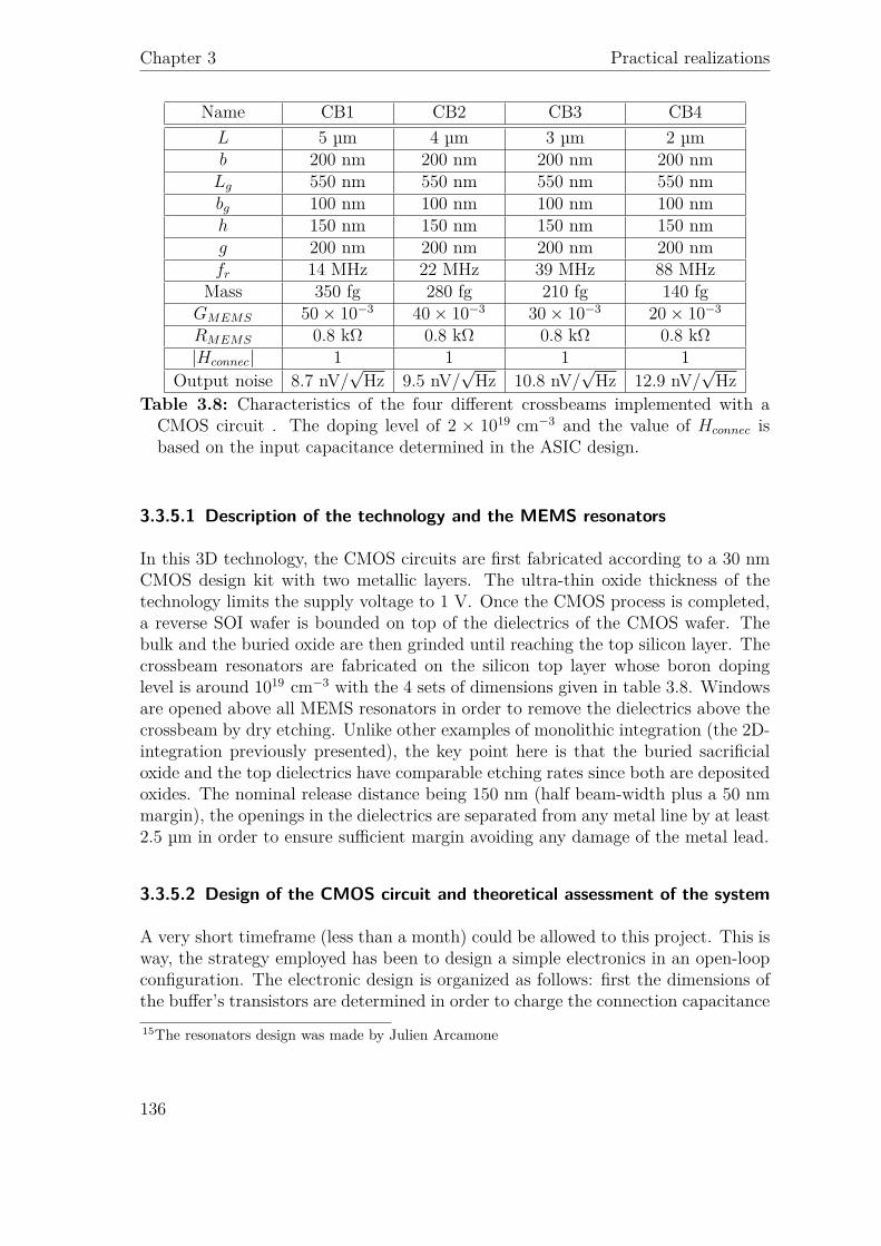
Chapter 3 Practical realizations
Name CB1 CB2 CB3 CB4
L 5 µm 4 µm 3 µm 2 µmb 200 nm 200 nm 200 nm 200 nm
Lg 550 nm 550 nm 550 nm 550 nmbg 100 nm 100 nm 100 nm 100 nmh 150 nm 150 nm 150 nm 150 nmg 200 nm 200 nm 200 nm 200 nmfr 14 MHz 22 MHz 39 MHz 88 MHz
Mass 350 fg 280 fg 210 fg 140 fgGMEMS 50 ◊ 10≠3 40 ◊ 10≠3 30 ◊ 10≠3 20 ◊ 10≠3
RMEMS 0.8 kΩ 0.8 kΩ 0.8 kΩ 0.8 kΩ|Hconnec| 1 1 1 1
Output noise 8.7 nV/Ô
Hz 9.5 nV/Ô
Hz 10.8 nV/Ô
Hz 12.9 nV/Ô
Hz
Table 3.8: Characteristics of the four different crossbeams implemented with aCMOS circuit . The doping level of 2 ◊ 1019 cm≠3 and the value of Hconnec isbased on the input capacitance determined in the ASIC design.
3.3.5.1 Description of the technology and the MEMS resonators
In this 3D technology, the CMOS circuits are first fabricated according to a 30 nmCMOS design kit with two metallic layers. The ultra-thin oxide thickness of thetechnology limits the supply voltage to 1 V. Once the CMOS process is completed,a reverse SOI wafer is bounded on top of the dielectrics of the CMOS wafer. Thebulk and the buried oxide are then grinded until reaching the top silicon layer. Thecrossbeam resonators are fabricated on the silicon top layer whose boron dopinglevel is around 1019 cm≠3 with the 4 sets of dimensions given in table 3.8. Windowsare opened above all MEMS resonators in order to remove the dielectrics above thecrossbeam by dry etching. Unlike other examples of monolithic integration (the 2D-integration previously presented), the key point here is that the buried sacrificialoxide and the top dielectrics have comparable etching rates since both are depositedoxides. The nominal release distance being 150 nm (half beam-width plus a 50 nmmargin), the openings in the dielectrics are separated from any metal line by at least2.5 µm in order to ensure sufficient margin avoiding any damage of the metal lead.
3.3.5.2 Design of the CMOS circuit and theoretical assessment of the system
A very short timeframe (less than a month) could be allowed to this project. This isway, the strategy employed has been to design a simple electronics in an open-loopconfiguration. The electronic design is organized as follows: first the dimensions ofthe buffer’s transistors are determined in order to charge the connection capacitance
15The resonators design was made by Julien Arcamone
136
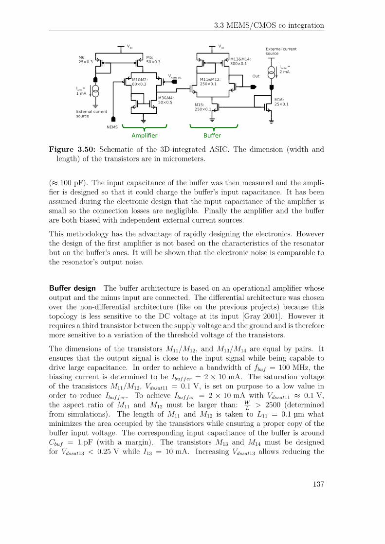
3.3 MEMS/CMOS co-integration
!"#!$%&'(')*
!*#!+%,'('),
!,%,'(')*
!-%$,(')*
./!0
1./!0234
5678
9
":7;
1<<
/=>?@A6B:CD@@?A>:EFD@C?
5GDHH?@
9
$:7;
!""#!"$%$,'(')"
!"*#!"+%*''(')"
!",%$,'(')"
!"-%$,(')"
ID>
/=>?@A6B:CD@@?A>EFD@C?
1<<
;78BJHJ?@ KDHH?@
Figure 3.50: Schematic of the 3D-integrated ASIC. The dimension (width andlength) of the transistors are in micrometers.
(¥ 100 pF). The input capacitance of the buffer was then measured and the ampli-fier is designed so that it could charge the buffer’s input capacitance. It has beenassumed during the electronic design that the input capacitance of the amplifier issmall so the connection losses are negligible. Finally the amplifier and the bufferare both biased with independent external current sources.
This methodology has the advantage of rapidly designing the electronics. Howeverthe design of the first amplifier is not based on the characteristics of the resonatorbut on the buffer’s ones. It will be shown that the electronic noise is comparable tothe resonator’s output noise.
Buffer design The buffer architecture is based on an operational amplifier whoseoutput and the minus input are connected. The differential architecture was chosenover the non-differential architecture (like on the previous projects) because thistopology is less sensitive to the DC voltage at its input [Gray 2001]. However itrequires a third transistor between the supply voltage and the ground and is thereforemore sensitive to a variation of the threshold voltage of the transistors.
The dimensions of the transistors M11/M12, and M13/M14 are equal by pairs. Itensures that the output signal is close to the input signal while being capable todrive large capacitance. In order to achieve a bandwidth of fbuf = 100 MHz, thebiasing current is determined to be Ibuffer = 2 ◊ 10 mA. The saturation voltageof the transistors M11/M12, Vdssat11 = 0.1 V, is set on purpose to a low value inorder to reduce Ibuffer. To achieve Ibuffer = 2 ◊ 10 mA with Vdssat11 ¥ 0.1 V,the aspect ratio of M11 and M12 must be larger than: W
L> 2500 (determined
from simulations). The length of M11 and M12 is taken to L11 = 0.1 µm whatminimizes the area occupied by the transistors while ensuring a proper copy of thebuffer input voltage. The corresponding input capacitance of the buffer is aroundCbuf = 1 pF (with a margin). The transistors M13 and M14 must be designedfor Vdssat13 < 0.25 V while I13 = 10 mA. Increasing Vdssat13 allows reducing the
137
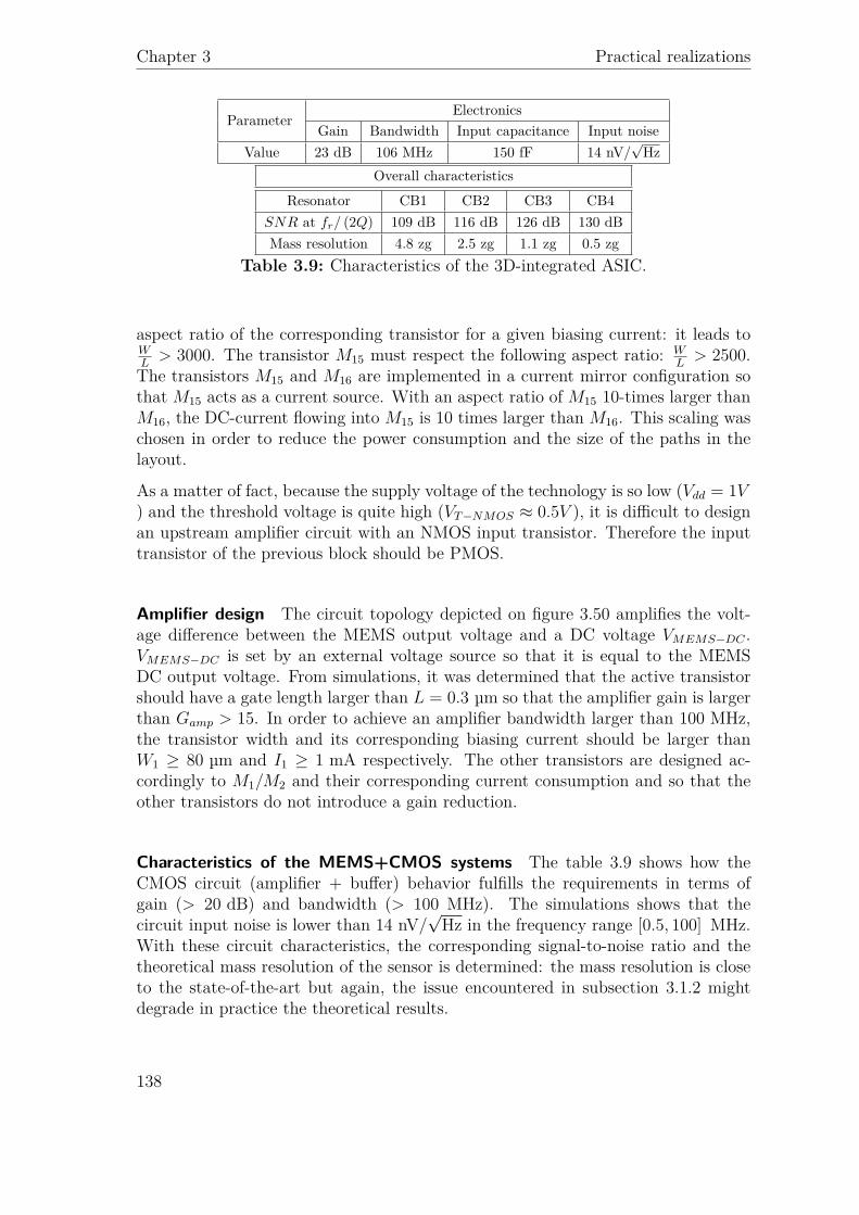
Chapter 3 Practical realizations
ParameterElectronics
Gain Bandwidth Input capacitance Input noise
Value 23 dB 106 MHz 150 fF 14 nV/Ô
Hz
Overall characteristics
Resonator CB1 CB2 CB3 CB4
SNR at fr/ (2Q) 109 dB 116 dB 126 dB 130 dB
Mass resolution 4.8 zg 2.5 zg 1.1 zg 0.5 zg
Table 3.9: Characteristics of the 3D-integrated ASIC.
aspect ratio of the corresponding transistor for a given biasing current: it leads toWL
> 3000. The transistor M15 must respect the following aspect ratio: WL
> 2500.The transistors M15 and M16 are implemented in a current mirror configuration sothat M15 acts as a current source. With an aspect ratio of M15 10-times larger thanM16, the DC-current flowing into M15 is 10 times larger than M16. This scaling waschosen in order to reduce the power consumption and the size of the paths in thelayout.
As a matter of fact, because the supply voltage of the technology is so low (Vdd = 1V
) and the threshold voltage is quite high (VT ≠NMOS ¥ 0.5V ), it is difficult to designan upstream amplifier circuit with an NMOS input transistor. Therefore the inputtransistor of the previous block should be PMOS.
Amplifier design The circuit topology depicted on figure 3.50 amplifies the volt-age difference between the MEMS output voltage and a DC voltage VMEMS≠DC .VMEMS≠DC is set by an external voltage source so that it is equal to the MEMSDC output voltage. From simulations, it was determined that the active transistorshould have a gate length larger than L = 0.3 µm so that the amplifier gain is largerthan Gamp > 15. In order to achieve an amplifier bandwidth larger than 100 MHz,the transistor width and its corresponding biasing current should be larger thanW1 Ø 80 µm and I1 Ø 1 mA respectively. The other transistors are designed ac-cordingly to M1/M2 and their corresponding current consumption and so that theother transistors do not introduce a gain reduction.
Characteristics of the MEMS+CMOS systems The table 3.9 shows how theCMOS circuit (amplifier + buffer) behavior fulfills the requirements in terms ofgain (> 20 dB) and bandwidth (> 100 MHz). The simulations shows that thecircuit input noise is lower than 14 nV/
ÔHz in the frequency range [0.5, 100] MHz.
With these circuit characteristics, the corresponding signal-to-noise ratio and thetheoretical mass resolution of the sensor is determined: the mass resolution is closeto the state-of-the-art but again, the issue encountered in subsection 3.1.2 mightdegrade in practice the theoretical results.
138

3.3 MEMS/CMOS co-integration
Figure 3.51: Layout view of a crossbeam 3D-integrated with its readout circuit
3.3.5.3 Layout of the resonator+ASIC
The figure 3.51 presents the layout of the crossbeam resonator 3D-integrated withthe CMOS circuit. The differential amplifier is located next to the resonator andthe buffer covers the rest of the area between the two contact pads. Overall the totalarea occupied by the resonator and the readout circuit is around 100 ◊ 100 µm2.The area covered by the amplifier is however similar to the one occupied by thecrossbeam resonator and thus highlights the interest of 3D-integration for arrays ofsensors. In fact, in the future, they could even be superposed to optimize the spaceoccupation.
3.3.6 Conclusion of MEMS/CMOS co-integration
This section presents three implementations of MEMS co-integrated with CMOScircuitry, progressing from the simplest integration scheme (2D-integration of a ca-pacitively detected MEMS) to more complex fabrication processes (3D-integrationof piezoresistively detected MEMS). The design of the electronic circuit was keptsimple to compensate for eventual process vagaries. Several electronic designs werecompared in order to establish the most suitable architecture. The CMOS circuitscharacterized in the different projects are functional but their performances aresomewhat lower than that predicted in the simulations.
The 2D co-integration of a capacitively detected MEMS based on a mature CMOSprocess has electrical characterics very similar to the simulations. The CMOS pro-cess was thus only marginally affected by the modification introduced by the MEMSfabrication. This opens the possibility of designing more complex electronic circuitryin order to fabricate complete sensors or array of sensors. The 2D co-integration of
139

Chapter 3 Practical realizations
Realization fr Responsitivity MEMS material MEMS-CMOS
pixel area
2D co-integration of a
capacitively detected MEMS
6 MHz 1.2 Hz/ag Single-crystal silicon ¥ 80 ◊ 60 µm2
2D co-integration of a
piezoresistively detected
MEMS
100 MHz 4700 Hz/ag Single-crystal silicon ¥ 30 ◊ 30 µm2
3D co-integration of a
piezoresistively detected
MEMS
88 MHz 310 Hz/ag Single-crystal silicon ¥ 30 ◊ 30 µm2
2D co-integration of a
capacitively detected MEMS
in [Verd 2006]
60 MHz 1.9 Hz/ag Aluminium NI
2D co-integration of a
capacitively detected MEMS
in [Uranga 2005]
100 MHz 12 Hz/ag Polysilicon ¥ 300 ◊ 300 µm2
2D co-integration of a
capacitively detected MEMS
in [Teva 2007]
182 MHz 98 Hz/ag Polysilicon ¥ 300 ◊ 300 µm2
Table 3.10: Comparison of the characteristics of the different co-integrated systems.
a piezoresistive detected MEMS process, however, was more affected by the tech-nological adaptations. Additional process engineering is thus required to obtain amore complete and reliable product.
The MEMS-CMOS preliminary measurements show that with a 2D co-integrationscheme, it is possible to measure the mechanical response of a 100 MHz-nanoresonatorusing a homodyne detection. Indeed, implementing the resonator close to the elec-tronics reduces both the connection losses and the feed-through transmission. Al-though further measurements are needed, the realization of complete closed-loopSOL seems possible because in this case, the actuation electrodes are removed.
Table 3.10 summarizes the characteristics of the 3 co-integrated designs presentedin the manuscript. It also compares them to different realizations described inthe literature. One can see that the capacitively detected resonator realized isoriginal because it is fabricated from single-crystal silicon (what should enhance itsquality factor) and because the area consumption of the MEMS-CMOS pixel is verysmall. Its performance expressed in terms of responsitivity is however limited andis difficult to improve because of the issues raised by the capacitive detection (issuedetailed in sections 2.4 and 3.3.2). Piezoresistive detection on the other presentsa high detection gain and a low output impedance that permit to fabricate lightnanoresonators with high resonant frequency.
140

3.4 Conclusion
3.4 Conclusion
This chapter focused on designs and characterizations of self-oscillating loops, fromthe proof-of-concept of a single oscillator to integrated sensors that can be imple-mented in arrays. The former uses stand-alone MEMS resonators self-oscillatedwith discrete electronics. The overall area of the sensors is around 200 ◊ 200 mm2
(without optimization) making it difficult to implement the sensors in large arrays.
The first work related to piezoelectric cantilevers showed that it is possible to re-alize self-oscillating loops despite the large intrinsic feed-through inherent to suchcomponents. Different techniques for estimating the frequency resolution have beencompared and the pros and cons of each were detailed. Overall, the frequency resolu-tion of the self-oscillation loops is degraded compared to that of the frequency-lockedloop probably due to the large feed-through at lower frequencies. In general, becauseof its low piezoelectric layer thickness and high frequency resolution, the resonatorshows a true potential for gas sensing with 10 ppb resolution for DMMP vapors.The second self-oscillating loop uses a crossbeam resonator that should have an ex-cellent mass resolution. To design a crossbeam-based SOL required investigation ofdifferent feed-through reduction techniques. This oscillator uses simple electronicsand has a frequency resolution similar to that of more complex measurement setupscomposed of an FLL-architecture with a downmixing implementation. The majornoise sources in the loop were characterized and compared to the closed-loop phase-noise. Close to the carrier, the phase noise is dominated by flicker noise that limitsthe frequency resolution of the sensors. The origin of this noise remains unclearand is under investigation. Overall, the latter sensor has a performance close to thestate-of-the-art of mass measurements and with faster response times.
In the second section, the design of an ASIC is described. This circuit addresses mul-tiple crossbeam resonators and comprises 4 self-oscillating loops and their associatedfrequency counters. The proposed implementation makes it possible to monitor 4or more sensors in a compact area. The problems associated with coupling betweenthe sensors can be assessed because each oscillator can be deactivated and its oscil-lating frequency can be measured in series or in parallel. Each self-oscillating loopis composed of an analog front-end that amplifies and filters the resonator outputsignal. The amplified signal was digitized in order to use a delay-lock loop as aphase-shifter. The architecture allows the phase-shift to be adjusted finely and in-dependently of the frequency. The oscillation amplitude is also controlled with easeby the supply voltage of the digital electronics. Finally, the ASIC was fabricated asa proof of concept so that similar circuits can be monolithically integrated with theMEMS resonator.
The last section focused on the monolithic integration of MEMS resonators withtheir readout electronics. It describes three different projects in which the MEMScomponent is fabricated next to the CMOS circuit (2D-integration) or above it(3D-integration). The prospect of fabricating compact sensors composed of the
141
Chapter 3 Practical realizations
resonators and the feedback electronics is explored. The area consumption of thesensors is 100 ◊ 100 µm2 or less and respects the requirements of arrays of sensors.The tested circuits were all functional but their performances varied. The resultsdemonstrate that the modifications introduced in the CMOS fabrication do not af-fect the viability of the circuit. The preliminary measurements of MEMS-CMOScomponents are satisfactory but further work is required to reduce the feed-throughtransmission so as to operate the resonator in a closed-loop. The presented fully inte-grated MEMS-CMOS structures are therefore the first steps towards the realizationof large arrays of MEMS-based sensors.
142

General conclusion
During my three years of PhD studies, I explored the use of MEMS resonators inapplications that require precise measurement of physical properties. This promis-ing research field involves several scientific domains. To fabricate a sensor from aMEMS resonator, the architecture of the overall system (composed of the MEMScomponent and the complementary electronics) must be analyzed; the design of theelectronics and the mechanical resonator must be optimized; and finally, the inher-ent practical constraints imposed by the fabrication and characterization processmust be surmounted.
In the first chapter, I summarize the requirements and performance of different archi-tectures that can monitor the resonant frequency variations of a MEMS component.Even though my PhD focuses on MEMS resonators (as they are used for mass sens-ing) this chapter is common to all micro- or nanoresonators. I established that inorder to obtain a sensor with a large dynamic range, a closed-loop architecture isrequired to dynamically track the resonant frequency of the MEMS component. Twomajor closed-loop architectures are described in the literature: self-oscillating loopsand frequency-locked loops. My research focused on self-oscillating loops becausetheir architecture is more compact and better suited to the fabrication of arrays ofsensors. In the same chapter, I present the limitations and the constraints imposedby this architecture. Certain aspects of the feed-through and the non-linearity hadpreviously been considered problematic. I confirm this by demonstrating that thefeed-through not only degrades the frequency resolution of the sensors but also canmake the oscillator unstable. In addition, the non-linearity introduced by the res-onator or electronics can amplify the colored noise around the carrier. The lastsection of the chapter describes different frequency measurement techniques, theiroperation principles and the advantages and disadvantages of each technique.
The second chapter focuses on the MEMS topologies and implementation schemesthat are suitable for mass spectrometry. I describe four MEMS resonators: (i) aclamped-clamped beam with electrostatic actuation and capacitive detection, (ii)a clamped-clamped beam with electrostatic actuation and piezoresistive detection,(iii) a resonator with the shape of a crossbeam, an electrostatic actuation and apiezoresistive detection, and (iv) a cantilever with piezoelectric actuation and de-tection. I assess their electromechanical transduction and their theoretical mass res-olution. In order to properly compare the performances of each MEMS resonator,the MEMS-to-electronics connection was incorporated into the model. I describethree major integration schemes: stand-alone resonators, and 2D- or 3D-integration
143

General conclusion
of MEMS and electronics. Each integration scheme is electrically modeled from atypical layout design to assess its feed-through and its connection losses. The elec-trical model leads to analytical formulae that were verified by electrical simulations.The stand-alone fabrication process was found to have the worst performance butit is the cheapest. On the other hand, the 2D-integration fabrication process hasfew electrical limitations but its technological development is often too expensivefor industrial applications.
Piezoresistive crossbeams and piezoelectric resonators have the best mass resolu-tions. The crossbeam benefits from a more complex mechanical structure than clas-sic beams which improves its piezoresistive detection. The piezoelectric cantileverbenefits from a linear electromechanical transduction scheme with high gain but itstechnological stack can be expensive to develop. In the last section of the chapter, Ianalyze the benefits of implementing an array of parallel and collectively addressedresonators. Although it is commonly assumed that implementing MEMS resonatorsin parallel arrays reduces the phase-noise of the array (compared to that of a singleresonator), I show that the circuit introduces an electrical limit. This limit must beevaluated to properly assess the performance of such an array.
In the last chapter, I describe the designs and practical realizations made during myPhD project. I first present the construction and characterization of a self-oscillatingloop using stand-alone resonators (a piezoelectric cantilever and a crossbeam) andcommercial electronic components. A major difficulty with the piezoelectric can-tilever is the V-shaped feed-through behavior which requires careful filtering to pre-vent parasitic oscillations in the loop. The frequency resolution was then measuredwith different techniques, each having their pros and cons. The frequency resolu-tions measured with the different techniques are similar but lower than those ob-tained with an FLL-architecture. With the latter architecture, the MEMS resonatorproduced good performance for gas sensing: a resolution of 10 ppb was achieved forDMMP vapors. The difference in frequency resolution between the two architecturesis believed to be due to the large feed-through at low frequency that accentuatedthe noise. This oscillator yields practical information on how to construct a low-costgas sensor. The second self-oscillating loop uses a crossbeam resonator. The majorchallenge in the design of the loop was to develop a measurement setup that limitsthe crosstalk within the resonator chip and in access to the chip. The frequencyresolution of the loop was similar when measured using temporal and frequencyacquisition. The frequency resolution of the self-oscillating loop was found to besimilar to that of a frequency-locked loop but in both architectures, a flicker noisedegrades the resolution of the sensor compared to that predicted by the model de-veloped in the previous chapter. In the second section of the final chapter, I presentthe design of an ASIC that can self-oscillate four crossbeams in parallel. The ASICincludes four frequency counters that allow it to measure simultaneously the res-onance frequency of the four MEMS components. The ASIC incorporates analogand digital electronics. The crossbeam output signal is first amplified and filteredusing analog circuits. The signal is then digitized to simplify the architecture of the
144

General conclusion
phase shifter while achieving good control. The coupling within the array, a probleminherent to arrays of sensors, could be evaluated with the ASIC design. Moreover,because of its small dimensions (7 ◊ 7 mm2), the ASIC can also be implemented inan array comprising 12 or more resonators.
In the last section of the chapter, the principal technological challenge inherent tothe fabrication of large arrays of MEMS sensors is explored, namely co-integrationof the MEMS and the electronic circuit on the same die. This technological stepis necessary towards the construction of arrays incorporating millions of sensorsbecause alternative integration schemes would require too many wire connections.This topic was explored in three projects in which the resonators are either 2D or 3Dco-integrated with the electronics. In the first project, I realized different electroniccircuits that address 2D co-integrated MEMS resonators with capacitive detection.The second project uses a technological process, developed in Leti, that makes thefabrication more flexible and allows the construction of 2D co-integrated nanowiresand crossbeam resonators. This design incorporates resonators with very high reso-nance frequency (> 100 MHz). In the third project, I designed a high-performanceamplifier and a buffer to interface with 3D co-integrated crossbeam resonators. TheMEMS/CMOS co-integrated chips are currently being manufactured and their per-formance should be evaluated in the next months.
Based on the realization of the self-oscillating loop including a crossbeam resonator,a future goal could be to further investigate the origin of the close to carrier flickernoise that limits the performance of the mechanical resonator. Another objectivewould be to understand why the frequency resolution of the oscillator is improperlyevaluated when the frequency counter measures the time lapse between consecutiverising edges. In this context, it would be interesting to operate temporal simulationsof a closed-loop with different phase-noise levels and frequency spectra in order toevaluate the limits of the frequency measurement technique. Such simulations aredifficult to implement, however, as they are very time consuming.
As described in the manuscript, an integrated circuit was designed and is beingfabricated. Obviously, it would be interesting to verify the functionality of thecircuitry and then to implement it with one or more resonators. The couplingbetween the different resonators and sustaining electronics should be assessed toevaluate whether medium dense arrays implemented with stand-alone resonatorscan be realized. Two approaches could be considered if a second version of theintegrated circuit was to be designed. If supplementary manpower can be assignedto the design of such circuitry, the experience acquired with the first realization mightallow them to implement a frequency-locked loop architecture in the chip. Anotherpossible approach would be to maintain the self-oscillating loop architecture, but tosimplify the circuitry based on the experience acquired with the first realized chip sothat the second version would be more compact. An interesting objective would beto construct an integrated circuit capable of self-oscillating 10 or more resonators.
Finally, the first realizations of MEMS-CMOS co-integrated systems are probably
145

General conclusion
the most promising outcome of my research. The preliminary measured character-istics of such systems are very satisfactory and indeed very promising. Obviouslyit would be very exciting to compare their characteristics with the other mentionedco-integrated implementations, once they are constructed. This integration schemeis very new in our group and rare in the literature, and it clearly offers many per-spectives. The electronic architectures usually employed for resonators should berethought in order to fulfill the particular demands of nanoresonators. Furthermorewhen comparing the minute areal demands of a NEMS component with the largerdemands of its release area and the area of associated feedback electronics, it isevident that there is an unsatisfactory filling factor. A possible improvement is therealization of a mixed array that would consist of individually addressing compactoscillators as described in section 3.3, with the modification that the resonator isreplaced by a small array of collectively addressed resonators. To conclude, NEMS-CMOS oscillators co-integrated into compact pixels are very new and rarely treatedin the literature. Any exploratory work in the domain promises to uncover newphysical phenomenon at the nanoscale level as well as promising new applicationsof the technology.
146

Nomenclature
ADEV Allan deviation
AGC Automatic gain control
AVAR Allan variation
AlN Aluminum Nitride
ASIC Application specified integrated circuit
CMOS Complementary metal oxide semiconductor
FLL Frequency lock loop
LNA Low-noise amplifier
MEMS MicroElectroMechanical Systems
NEMS NanoElectroMechanical Systems
SOI Silicon on insulator
SOL Self-oscillating loop
VCO Voltage-controlled Oscillator
Dkit Design kit
DLL Delay lock loop
DMMP Dimethyl Methylphosphonate is Sarrin gas simulant
FDSOI Fully depleted silicon on insulator
NMOS Negatively doped metal–oxide–semiconductor field-effect transis-tor
PLL Phase lock loop
ppb Particule per billion
147

Nomenclature
ppm Particule per million
PSD Power spectral density
–(t) Relative amplitude noise
∆Φg0 Resistivity variation of the gauge
∆Φg Resistivity variation of the gauge
∆bg Width variation of the gauge
∆C (t) Capacitance variation in the capacitive detection
∆f Frequency difference
∆f Resonance frequency variation
∆hg Thickness variation of the gauge
∆Lg Length variation of the gauge
∆m Added mass
”t Sampling time of the reference clock
∆„ Phase difference
∆ÂMEMS(f) Phase-shift difference between the MEMS phase-shift at f and atfr
∆Âref Desired phase-shift difference
∆ÂSBR Signal-to-background ratio phase-shift
¸1 Strain of the beam
÷K Coefficient for the Duffing effect
÷A Actuation normalization constant
÷D Detection coefficient
Γτ Auto-correlation function
“beam Gauge factor
“Si Gauge factor of the silicon
Ÿmass Normalization coefficient that depends on how ∆m is added tothe beam
148

Nomenclature
ŸH Hooge noise coefficient
⁄ Modal coefficient ????
¸ Tensor of the strain
Σ Tensor of the stress
Á Permittivity of the piezoelectric crystal
c Elastic stiffness constant
D Electric displacement
E Electric field
e Piezoelectric constant
ÈfÍ Mean value of the frequency
ÈT Í Mean value of the period
w (x, t) Displacement of the beam
E Statistical expectation
vact(t) Actuation voltage
vnoise(t) voltage noise
v(t) Voltage signal
µN Electron mobility of the transistor
Φg0 Resistivity of the gauge at rest
ΦSi0 Silicon resistivity at rest
ÂMEMS Phase-shift introduced by the MEMS resonator
Ÿ Responsitivity of the MEMS resonator
fl Density of the beam
fleq Equivalent mass of the beam per unit of surface
‡fr Frequency resolution
‡m Minimal detectable mass
149

Nomenclature
· Delay
Υn (x) Spacial variable in the Galerkin decomposition
Á0 Permittivity of the air
Ï(t) Phase noise
› Coefficient of the viscosity of the beam
an (t) Temporal variable in the Galerkin decomposition
b Width of the beam
C (t) Capacitance
C0 Electrostatic capacitance when the beam is at rest
cbeam Modulus of the beam
CBOX Capacitance of the BOX
Celec Electronics input capacitance
Cm Motion capacitance in the BVD model
Coutput Capacitance at the output of the resonator
Cox Oxide capacitance per unit of area
CP ZE0 Static capacitance of the piezoelectric layer at fr
CP ZE AlN-layer capacitance
CP ZE Static capacitance of the piezoelectric layer
Cp On-chip routing parasitic capacitance
d Dielectric losses
D Doping level
f Frequency
fact Actuation frequency
fCLK Frequency of the reference clock
fc Cut-off frequency of the high- or low-pass filter
150

Nomenclature
ffilter Cut-off frequency of the filter
fk Instantaneous frequency
Fl≠c Critical actuation force
FlN (f) Complex amplitude of the negative force applied on the beam perunit of length
FlP (f) Complex amplitude of the positive force applied on the beam perunit of length
Fl(f) Complex amplitude of the actuation force
Fl (t) Force applied on the beam per unit of length
fosc Oscillation frequency
fr0 Resonance frequency corresponding to an added mass null
fr Resonance frequency of the MEMS component
f∆mr Resonance frequency corresponding to an added mass ∆m
fsource Frequency of the signal source
fV CO Gain of the VCO
g Gap
Gamp Amplifier gain
Gfilter Low-frequency gain of the filter
gg Width of the piezoresistive gauge
gMEMS Gain of the MEMS resonator at fr
GSBR Signal-to-background ratio gain
h Thickness of the beam
Hϕ(f) Transfer function of the open to closed loop noise
Hact Transfer function of the MEMS actuation
Hconnec(f) Transfer function of the MEMS-to-electronics connection
Hdelay(f) Transfer function of the delay bloc
151

Nomenclature
Hdet Transfer function of the MEMS detection
Helec≠NL(f) Transfer function of the electronics including the nolinearity
Helec(f) Transfer function of the electronics
Hfilter Transfer function of the filter
HF LL(f) Transfer function frequency lock loop
Hft(f) Transfer function of the transmission feed-through
hg Thickness of the piezoresistive gauge
HHP F (f) Transfer function of the high-pass filter
HLP F (f) Transfer function of the low-pass filter
HMEMSft(f) Transfer function of MEMS resonator including the transmissionfeed-through
HMEMS(f) Transfer function of the MEMS resonator
HphaseMEMS(f) Transfer function of the MEMS in the phase representation
HOL(f) Open-loop transfer function
HP LL(f) Transfer function of the PLL
HD2 Second order harmonic distorsion
HD3 Third order harmonic distorsion
I Moment of inertia of the beam
i (t) Current
k Stiffness of the MEMS resonator
kd Proportional gain
kB Boltzmann constant
L Length of the beam
L Length of the vibrating mass
LA Active transistor length
Lbonding Inductance introduced by the wire-bonding
152

Nomenclature
Lg Length of the piezoresistive gauge
Lm Motion inductance in the BVD model
Ltech Minimum transistor length imposed by the CMOS process
M Number of elements fk
m Mass of the MEMS resonator
M Momentum applied on a beam
Mbonding Mutual coefficient introduced by the wire-bonding
n Integer
Pamp Power consumption of the amplifier
pft V-shape feed-through frequency coefficient
Q Quality factor of the resonator
QV CO Quality factor of the VCO
R Resistance
req Equivalent beam rigidity
Rg0 Resistance of the gauge at rest
Rlat Lateral resistance in the substrate between two paths
RMEMS Output impedance of the MEMS resonator
Rm Motion resistance in the BVD model
Rsub Resistance from the BOX/silicon bulk interface to the ground
Sδf/f Power spectral density of the relative frequency noise
Sδf/f (f) Power spectral density of the relative frequency variations
S∆fV CO(f) Power spectral density output frequency noise of the VCO
Sϕ≠ideal(f) Ideal power spectral density of the SOL phase noise
SϕMEMS+elec(f) Power spectral density of the phase-noise
Sϕout(f) Power spectral density of the output phase noise
153

Nomenclature
SϕV CO(f) Power spectral density of the VCO output phase-noise
Selec Power spectral density of the electronic noise
Sf (f) Power spectral density of the frequency noise
Siamp PSD of the amplifier input current noise
SMAPower spectral density generated by the transistor MA
SMEMSth(f) Power spectral density of the MEMS noise except the thermome-
chanical noise
SP ZR Power spectral density of the piezoresistive gauge
Sthermo(f) Power spectral density of the thermomechanical noise
Su(f) Power spectral density of the input signal of the VCO
Svmems(f) Power spectral density of velec
Svamp PSD of the amplifier input voltage noise
SBR Signal-to-background ratio
SNR Signal-to-noise ratio
T Temperature
t Time
T (w) Intern stress in the beam
Tk Instantaneous period
tk kth transistion time
Tmeas≠opt Optimal measurement duration
Tmeas Measurement duration
u(f) Input signal of the VCO
V (t) Voltage
v0 Amplitude voltage
vact≠c Critical actuation voltage
vact(f) Complex amplitude of the actuation voltage
154
Nomenclature
Vdd Supply voltage of the CMOS technology
Vdssat Drain-Source saturation voltage
velec(f) Complex amplitude of the electronic input signal
Vg Applied voltage on the gauge
vMEMS(f) Complex amplitude of the unloaded resonator output voltage
w (f) Complex amplitude of the mechanical displacement of the beam
w (t) Mechanical displacement of the beam
WA Active transistor width
x Coordinate along the length of the beam
y(f) Complex amplitude of the mechanical displacement
yc Critical mechanical displacement
Yin Input admittance of the MEMS resonator for a single actuation
Y inN Negative input admittance of the MEMS resonator in differentialactuation
Y inP Positive input admittance of the MEMS resonator in differentialactuation
z0 Coordinate of the neutral line
155


Bibliography
[Aebersold 2003] R. Aebersold and M. Mann. Mass spectrometry-based proteomics.Nature, vol. 422, no. 6928, pages 198–207, Mar 2003.
[Akgul 2009] M. Akgul, K. Bongsang, L.-W. Hung, Y. Lin, W.-C. Li, W.-L. Huang,I. Gurin, A. Borna and C.T.-C. Nguyen. Oscillator far-from-carrier phasenoise reduction via nano-scale gap tuning of micromechanical resonators.pages 798 –801, June 2009.
[Albrecht 1991] T. R. Albrecht, P. Grutter, D. Horne and D. Rugar. Frequencymodulation detection using high-Q cantilevers for enhanced force microscopesensitivity. Journal of Applied Physics, vol. 69, no. 2, pages 668–673, Jan1991.
[Arcamone 2007] J. Arcamone, B. Misischi, F. Serra-Graells, M. A. F. van denBoogaart, J. Brugger, F. Torres, G. Abadal, N. Barniol and F. Perez-Murano.A Compact and Low-Power CMOS Circuit for Fully Integrated NEMS Res-onators. TCAS II, vol. 54, no. 5, pages 377 –381, May 2007.
[Arcamone 2009] J. Arcamone, M. Sansa, J. Verd, A. Uranga, G. Abadal,N. Barniol, M.A.F. van den Boogaart, J. Brugger and F. Perez-Murano.Nanomechanical mass sensor for monitoring deposition rates through con-fined apertures. In Nano/Micro Engineered and Molecular Systems, 2009.NEMS 2009. 4th IEEE International Conference on, pages 94 –97, Jan 2009.
[Arcamone 2010] J. Arcamone, E. Colinet, A. Niel and E. Ollier. Efficient capac-itive transduction of high-frequency micromechanical resonators by intrinsiccancellation of parasitic feedthrough capacitances. Applied Physics Letters,vol. 97, no. 4, pages 043505 –043505–3, Jul 2010.
[Arcamone 2011] J. et al. Arcamone. VLSI silicon multi-gas analyzer coupling gaschromatography and NEMS detectors. In to be published in the proc. of theIEEE IEDM, 2011.
[Arndt 2010] G. Arndt, E. Colinet and J. Juillard. Design of a co-integratedCMOS/NEMS oscillator with a simple electronic circuit. In Design Test In-tegration and Packaging of MEMS/MOEMS (DTIP), 2010 Symposium on,pages 368 –371, 2010.
[Arndt 2011] G. Arndt, E. Colinet, J. Arcamone and J. Juillard. A design method-ology for fully integrated MEMS and NEMS Pierce oscillators. Sensors andActuators A: Physical, vol. In Press, Corrected Proof, pages –, 2011.
157
Bibliography
[Bahreyni 2007] B. Bahreyni and C. Shafai. Oscillator and frequency-shift mea-surement circuit topologies for micromachined resonant devices. Sensors andActuators A: Physical, vol. 137, no. 1, pages 74 – 80, 2007.
[Bao 2000] M.H. Bao. Micro mechanical transducers: pressure sensors, accelerome-ters, and gyroscopes. Handbook of sensors and actuators. Elsevier, 2000.
[Bargatin 2005] I. Bargatin, E.B. Myers, J. Arlett, B. Gudlewski and M.L. Roukes.Sensitive detection of nanomechanical motion using piezoresistive signaldownmixing. Applied Physics Letters, vol. 86, no. 13, Mar 2005.
[Bargatin 2007] I. Bargatin, I. Kozinsky and M. L. Roukes. Efficient electrother-mal actuation of multiple modes of high-frequency nanoelectromechanical res-onators. Applied Physics Letters, vol. 90, no. 9, pages 093116–093116–3, Feb2007.
[Bargatin 2008] I. Bargatin. High-frequency nanomechanical resonators for sensorapplications. PhD thesis, California Institute of Technology, 2008.
[Barnes 1990] J. Barnes and D. Allan. Variances based on data with dead timebetween the measurements. Rapport technique, NIST technical notes 1318,1990.
[Bienstman 1995] J. Bienstman, H.A.C. Tilmans, M. Steyaert and R. Puers. AnOscillator Circuit For Electrostatically Driven Silicon-based One-port Res-onators. In Proc. and Eurosensors IX. Solid-State Sensors and ActuatorsTransducers ’95. The 8th International Conference on, volume 1, pages 146–149, 1995.
[Boisen 2000] A. Boisen, J. Thaysen, H. Jensenius and O. Hansen. Environmentalsensors based on micromachined cantilevers with integrated read-out. Ultra-microscopy, vol. 82, no. 1-4, pages 11 – 16, 2000.
[Boisen 2011] Anja Boisen, Soren Dohn, Stephan Sylvest Keller, Silvan Schmidand Maria Tenje. Cantilever-like micromechanical sensors. REPORTS ONPROGRESS IN PHYSICS, vol. 74, no. 3, MAR 2011.
[Brissaud 2003] M. Brissaud, S. Ledren and P. Gonnard. Modelling of a cantilevernon-symmetric piezoelectric bimorph. Journal of Micromechanics and Micro-engineering, vol. 13, no. 6, pages 832–844, Nov 2003.
[Burg 2007] T. Burg, M. Godin, S. Knudsen, W. Shen, G. Carlson, J. Foster,K. Babcock and S. Manalis. Weighing of biomolecules, single cells and sin-gle nanoparticles in fluid. Nature, vol. 446, no. 7139, pages 1066–1069, Apr2007.
[Calvo 2009] B. Calvo, N. Medrano, S. Celma and M.T. Sanz. A low-power high-sensitivity CMOS voltage-to-frequency converter. In Proc. 52nd IEEE Inter-national Midwest Symposium on Circuits and Systems MWSCAS ’09, pages118–121, Aug 2009.
158

Bibliography
[Campbell 2006] G.A. Campbell and R. Mutharasan. Use of piezoelectric-excitedmillimeter-sized cantilever sensors to measure albumin interaction with self-assembled monolayers of alkanethiols having different functional headgroups.Analytical Chemistry, vol. 78, no. 7, pages 2328–2334, Apr 2006.
[Chapuis 2007] F. Chapuis, E. Defay, F. Casset, J.F. Manceau, F. Bastien andM. Aid. Microswitch with Mixed Piezoelectric and Electrostatic Actuation.pages 1159 –1162, June 2007.
[Chiu 2008] H.-Y. Chiu, P. Hung, H.W.C. Postma and M. Bockrath. Atomic-ScaleMass Sensing Using Carbon Nanotube Resonators. Nano Letters, vol. 8,no. 12, pages 4342–4346, Dec 2008.
[Cleland 2002] A.N. Cleland and M.L. Roukes. Noise processes in nanomechanicalresonators. Journal of Applied Physics, vol. 92, no. 5, pages 2758–2769, Sep2002.
[Colinet 2009] E. Colinet, L. Duraffourg, S. Labarthe, S. Hentz, P. Robert andP. Andreucci. Self-oscillation conditions of a resonant nanoelectromechanicalmass sensor. Journal of Applied Physics, vol. 105, no. 12, pages 124908–8,2009.
[Colinet 2010] E. Colinet, J. Arcamone, A. Niel, E. Lorent, S. Hentz and E. Ollier.100 MHz oscillator based on a low polarization voltage capacitive Lamé;-mode MEMS resonator. In Frequency Control Symposium (FCS), 2010 IEEEInternational, pages 174 –178, June 2010.
[datasheet a] 33250A datasheet.
[datasheet b] CCSO-914X3-1000 datasheet.
[datasheet c] SR844 lock-in amplifier datasheet.
[Defosseux 2011] M. Defosseux, M. Allain, P. Ivaldi, E. Defay and S. Basrour. Highlyefficient piezoelectric micro harvester for low level of acceleration fabricatedwith a CMOS compatible process. pages 1859 –1862, June 2011.
[Demir 2000] A. Demir, A. Mehrotra and J. Roychowdhury. Phase noise in oscilla-tors: a unifying theory and numerical methods for characterization. Circuitsand Systems I: Fundamental Theory and Applications, IEEE Transactionson, vol. 47, no. 5, pages 655 –674, May 2000.
[Dohn 2005] S. Dohn, R. Sandberg, W. Svendsen and A. Boisen. Enhanced function-ality of cantilever based mass sensors using higher modes. Applied PhysicsLetters, vol. 86, no. 23, June 2005.
[Dohn 2007] S. Dohn, W. Svendsen, A. Boisen and O. Hansen. Mass and positiondetermination of attached particles on cantilever based mass sensors. Reviewof Scientific Instruments, vol. 78, no. 10, page 103303, 2007.
[Dohn 2010] S. Dohn, S. Schmid, F. Amiot and A. Boisen. Position and mass deter-mination of multiple particles using cantilever based mass sensors. AppliedPhysics Letters, vol. 97, no. 4, page 044103, 2010.
159

Bibliography
[Domon 2006] B. Domon and R. Aebersold. Review - Mass spectrometry and proteinanalysis. Science, vol. 312, no. 5771, pages 212–217, Apr 2006.
[Ekinci 2004a] K.L. Ekinci, X.M.H. Huang and M.L. Roukes. Ultrasensitive nano-electromechanical mass detection. Applied Physics Letters, vol. 84, no. 22,pages 4469–4471, May 2004.
[Ekinci 2004b] K.L. Ekinci, Y.T. Yang and M.L. Roukes. Ultimate limits to inertialmass sensing based upon nanoelectromechanical systems. Journal of AppliedPhysics, vol. 95, no. 5, pages 2682–2689, Mar 2004.
[Feng 2007] X.L. Feng, R.R. He, P.D. Yang and M.L. Roukes. Phase Noise and Fre-quency Stability of Very-High Frequency Silicon Nanowire NanomechanicalResonators. In Solid-State Sensors, Actuators and Microsystems Conference,2007. TRANSDUCERS 2007. International, pages 327 –330, 2007.
[Feng 2008] X.L. Feng, C.J. White, A. Hajimiri and M.L. Roukes. A self-sustainingultrahigh-frequency nanoelectromechanical oscillator. Nature Nanotechnol-ogy, vol. 3, no. 6, pages 342–346, June 2008.
[Gelb 1968] A. Gelb and W. Van der Velde. Multiple-input describing functions andnonlinear system design. Mcgraw-Hill, New-York, 1968.
[Giner 2011] J. Giner, A. Uranga, J.L. Muñoz-Gamarra, E. Marigó, E. Colinet,J. Arcamone and Barniol N. Cancellation of the Parasitic Current in anintegrated CMOS-MEMS Clamped- Clamped Beam Resonator. In 34th Inter-national Conference on Micro and Nano Engineering, 2011.
[Gray 2001] P. Gray, P. Hurst, S. Lewis and R. Meyer. Analysis and design of analogintegrated circuits. John Wiley & Sons, 2001.
[Hagleitner 2001] C. Hagleitner, A. Hierlemann, D. Lange, A. Kummer, N. Kerness,O. Brand and H. Baltes. Smart single-chip gas sensor microsystem. Nature,vol. 414, no. 6861, pages 293–296, Nov 2001.
[Harkey 2000] J.A. Harkey and T.W. Kenny. 1/f noise considerations for the designand process optimization of piezoresistive cantilevers. Microelectromechani-cal Systems, Journal of, vol. 9, no. 2, pages 226 –235, June 2000.
[He 2006] R. He and P. Yang. Giant piezoresistance effect in silicon nanowires.Nature Nanotechnology, vol. 1, no. 1, pages 42–46, Oct 2006.
[He 2008] R. He, X.L. Feng, M.L. Roukes and P. Yang. Self-transducing siliconnanowire electromechanical systems at room temperature. Nano Letters,vol. 8, no. 6, pages 1756–1761, June 2008.
[He 2010] L. He, Y. P. Xu and M. Palaniapan. A State-Space Phase-Noise Modelfor Nonlinear MEMS Oscillators Employing Automatic Amplitude Control.Circuits and Systems I: Regular Papers, IEEE Transactions on, vol. 57, no. 1,pages 189–199, Jan 2010.
160

Bibliography
[Ivaldi 2011a] P. Ivaldi, J. Abergel, H. Blanc, E. Colinet, E.B. Myers, M.L. Roukes,P. Andreucci, S. Hentz and E. Defay. DMMP vapor detection with 50nmthick AlN films based microcantilever. In Transducers 2011, 2011.
[Ivaldi 2011b] P. Ivaldi, J. Abergel, M.H. Matheny, L.G. Villanueva, R.B. Kara-balin, M.L. Roukes, P. Andreucci, S. Hentz and E. Defay. 50 nm thick AlNfilm-based piezoelectric cantilevers for gravimetric detection. Journal of Mi-cromechanics and Microengineering, vol. 21, no. 8, page 085023, 2011.
[Jensen 2008] K. Jensen, K. Kim and A. Zettl. An atomic-resolution nanomechan-ical mass sensor. Nature Nanotechology, vol. 3, no. 9, pages 533–537, Sep2008.
[Juillard 2009] J. Juillard, A Bonnoit, E. Avignon, S. Hentz, N. Kacem and E. Co-linet. Large amplitude motion of an electrostatically-actuated resonant beamoperated in closed-loop. Journal of Applied Physics, 2009.
[Kacem 2008] N. Kacem, S. Hentz, H. Fontaine, V. Nguyen, P. Robert, B. Legrandand L. Buchaillot. From MEMS to NEMS: Modelling and characterization ofthe non linear dynamics of resonators, a way to enhance the dynamic range.In NSTI Nanotech, volume 3, pages 619–622, 2008.
[Karabalin 2009] R.B. Karabalin, M.H. Matheny, X.L. Feng, E. Defay, G. Le Rhun,C. Marcoux, S. Hentz, P. Andreucci and M.L. Roukes. Piezoelectric nano-electromechanical resonators based on aluminum nitride thin films. AppliedPhysics Letters, vol. 95, no. 10, Sep 2009.
[Kharrat 2008] C. Kharrat, E. Colinet and A. Voda. HŒ Loop shaping control forPLL-based mechanical resonance tracking in NEMS resonant mass sensors.In Sensors, 2008 IEEE, pages 1135 –1138, Oct 2008.
[Kharrat 2009] C. Kharrat. Application des techniques de contrôle sur les réseauxde micro et nanostructures. PhD thesis, EEATS, 2009.
[Knobel 2008] R. Knobel. Mass sensors: Weighing single atoms with a nanotube.Nature Nanotechnology, vol. 3, no. 9, pages 525–526, Sep 2008.
[Kobayashi 2011] K. Kobayashi, H. Yamada and K. Matsushige. Reduction of fre-quency noise and frequency shift by phase shifting elements in frequency mod-ulation atomic force microscopy. Review of Scientific Instruments, vol. 82,no. 3, page 033702, 2011.
[Labarthe 2010] S. Labarthe. Conception et modélisation d’un nanocapteur de massepar détection piézorésistive. PhD thesis, Université Joseph Fourier, 2010.
[Lang 1998] H.P. Lang, R. Berger, F. Battiston, J.P. Ramseyer, E. Meyer, C. An-dreoli, J. Brugger, P. Vettiger, M. Despont, T. Mezzacasa, L. Scandella, H.J.Guntherodt, C. Gerber and J.K. Gimzewski. A chemical sensor based ona micromechanical cantilever array for the identification of gases and va-pors. Applied Physics A- Materials Science & Processing, vol. 66, no. Part
161

Bibliography
1, S, pages S61–S64, Mar 1998. 9th International Conference on ScanningTunneling Microscopy/Spectroscopy and Related Techniques, HAMBURG,GERMANY, JUL 20-25, 1997.
[Lee 2004] S.e Lee and C.T.-C. Nguyen. Mechanically-coupled micromechanical res-onator arrays for improved phase noise. In Proc. IEEE International Fre-quency Control Symposium and Exposition, pages 144–150, 2004.
[Lee 2009a] D. Lee, S. Kim, N. Jung, T. Thundat and S. Jeon. Effects of goldpatterning on the bending profile and frequency response of a microcantilever.Journal of Applied Physics, vol. 106, no. 2, Jul 2009.
[Lee 2009b] J.E.-Y. Lee and A.A. Seshia. Parasitic feedthrough cancellation tech-niques for enhanced electrical characterization of electrostatic microres-onators. Sensors and Actuators A: Physical, vol. 156, no. 1, pages 36 –42, 2009.
[Leeson 1966] D.B. Leeson. A simple model of feedback oscillateur noise spectrum.Proceedings of the institute of electrical and electronics engineers, vol. 54,no. 2, pages 329–&, 1966.
[Levy 2010] R. Levy, A. Dupret and H. Mathias. Phase noise analysis of the Fre-quency Tracking Oscillator. In Frequency Control Symposium (FCS), 2010IEEE International, pages 624 –628, June 2010.
[Li 2007] Mo Li, H. X. Tang and M. L. Roukes. Ultra-sensitive NEMS-based can-tilevers for sensing, scanned probe and very high-frequency applications. Na-ture Nanotechnology, vol. 2, no. 2, pages 114–120, Feb 2007.
[Li 2010] Mo Li, E.B. Myers, H.X. Tang, S.J. Aldridge, H.C. McCaig, J.J. Whiting,R.J. Simonson, N.S. Lewis and M.L. Roukes. Nanoelectromechanical Res-onator Arrays for Ultrafast, Gas-Phase Chromatographic Chemical Analysis.Nano Letters, vol. 10, no. 10, pages 3899–3903, Oct 2010.
[Lopez 2009a] J L Lopez, J Verd, J Teva, G Murillo, J Giner, F Torres, A Uranga,G Abadal and N Barniol. Integration of RF-MEMS resonators on submi-crometric commercial CMOS technologies. Journal of Micromechanics andMicroengineering, vol. 19, no. 1, page 015002, 2009.
[Lopez 2009b] J.L. Lopez, J. Verd, J. Giner, A. Uranga, G. Murillo, E. Marigo,F. Torres, G. Abadal and N. Barniol. High Q CMOS-MEMS resonators andits applications as RF tunable band-pass filters. pages 557 –560, June 2009.
[Mamin 2001] H.J. Mamin and D. Rugar. Sub-attonewton force detection at mil-likelvin temperatures. Applied Physics Letters, vol. 79, no. 20, pages 3358–3360, Nov 2001.
[Maraldo 2007] D. Maraldo and R. Mutharasan. Detection and Confirmation ofStaphylococcal Enterotoxin B in Apple Juice and Milk Using Piezoelectric-Excited Millimeter-Sized Cantilever Sensors at 2.5 fg/mL. Analytical Chem-istry, vol. 79, pages 7636–7643, 2007.
162

Bibliography
[Masmanidis 2007] S. Masmanidis, R. Karabalin, I. De Vlaminck, G. Borghs,M. Freeman and M.L. Roukes. Multifunctional nanomechanical systems viatunably coupled piezoelectric actuation. Science, vol. 317, no. 5839, pages780–783, Aug 2007.
[Mestrom 2009] R.M.C. Mestrom, R.H.B. Fey and H. Nijmeijer. Phase Feed-back for Nonlinear MEM Resonators in Oscillator Circuits. Mechatronics,IEEE/ASME Transactions on, vol. 14, no. 4, pages 423 –433, Aug 2009.
[Mile 2010] E. Mile, G. Jourdan, I. Bargatin, S. Labarthe, C. Marcoux, P. An-dreucci, S. Hentz, C. Kharrat, E. Colinet and L. Duraffourg. In-plane nano-electromechanical resonators based on silicon nanowire piezoresistive detec-tion. Nanotechnology, vol. 21, no. 16, Apr 2010.
[Naik 2009] A.K. Naik, M.S. Hanay, W.K. Hiebert, X.L. Feng and M.L. Roukes.Towards single-molecule nanomechanical mass spectrometry. Nature Nan-otechnology, vol. 4, no. 7, pages 445–450, Jul 2009.
[Oliveira 2010] J. Oliveira, J. Goes, M. Figueiredo, E. Santin, J. Fernandes andJ. Ferreira. An 8-bit 120-MS/s Interleaved CMOS Pipeline ADC Based onMOS Parametric Amplification. Circuits and Systems II: Express Briefs,IEEE Transactions on, vol. 57, no. 2, pages 105 –109, Feb 2010.
[Palmisano 2003] G. Palmisano and S. Pennisi. CMOS single-input differential-output amplifier cells. IEEE proceedings- Circuit Devices and Systems,vol. 150, no. 3, pages 194–198, June 2003.
[Paul 2006] M.R. Paul, M.T. Clark and M.C. Cross. The stochastic dynamics of mi-cron and nanoscale elastic cantilevers in fluid: fluctuations from dissipation.Nanotechnology, vol. 17, no. 17, pages 4502–4513, Sep 2006.
[Roukes 2007] M.L. Roukes. Nanoelectromechanical systems: Potential, progress, &projections. In Proc. MEMS Micro Electro Mechanical Systems IEEE 20thInternational Conference on, pages 93–94, Jan 2007.
[Rubiola 2008] E. Rubiola. Phase noise and frequency stability in oscillators. Cam-bridge University Press, 2008.
[Russell 1997] D.H. Russell and R.D. Edmondson. High-resolution mass spectrome-try and accurate mass measurements with emphasis on the characterizationof peptides and proteins by matrix-assisted laser desorption/ionization time-of-flight mass spectrometry. Journal of Mass Spectrometry, vol. 32, no. 3,pages 263–276, Mar 1997.
[Sansen 2006] W. Sansen. Analog design essentials. Spinger, 2006.
[Sinha 2009] N. Sinha, G.E. Wabiszewski, R. Mahameed, V.V. Felmetsger, S.M.Tanner, R.W. Carpick and G. Piazza. Piezoelectric aluminum nitride na-noelectromechanical actuators. Applied Physics Letters, vol. 95, no. 5, Aug2009.
163

Bibliography
[Sta 1988] IEEE standard on piezoelectricity. 1988.
[Susplugas 2004] O. Susplugas. Application des boucles à verrouillage de retard àla synthèse de fréquences dans les circuits pour les communications mobiles.PhD thesis, Ecole Nationale Supérieure des Télécommunications de Paris,2004.
[Tang 2002] H.X. Tang, X.M.H. Huang, M.L. Roukes, M. Bichler and W. Wegschei-der. Two-dimensional electron-gas actuation and transduction for GaAs na-noelectromechanical systems. Applied Physics Letters, vol. 81, no. 20, pages3879–3881, Nov 2002.
[Taylor 2010] J.D. Taylor, B. Elliott, Dickel D., G. Keskar, J. Gaillard, M. J. Skoveand A. M. Rao. Oxford handbook of nanoscience and technology, volume 2.Frontiers in Nanoscience and Nanotechnology, 2010.
[Teva 2007] J. Teva, G. Abadal, A. Uranga, J. Verd, F. Torres, J.L. Lopez, J. Esteve,E. Perez-Murano and Barniol N. VHF CMOS-MEMS resonator monolith-ically integrated in a standard 0.35?m CMOS technology. In Micro ElectroMechanical Systems, 2007. MEMS. IEEE 20th International Conference on,pages 779 – 782, 2007.
[Thevenin 1883] L. Thevenin. Sur un nouveau théorème d’électricité dynamique [Ona new theorem of dynamic electricity]. Comptes Rendus hebdomadaires desséances de l’Académie des Sciences, vol. 97, pages 159–161, 1883.
[Uranga 2005] A. Uranga, J. Teva, J. Verd, J.L. López, F. Torres, J. Esteve,G. Abadal, F. Pérez-Murano and N. Barniol. Fully CMOS integrated lowvoltage 100 MHz MEMS resonator. Electronics Letters, vol. 41, no. 24, pages1327–1328, 2005.
[Van Dyke 1928] K.S. Van Dyke. The Piezo-Electric Resonator and Its EquivalentNetwork. Proceedings of the Institute of Radio Engineers, vol. 16, no. 6,pages 742 – 764, June 1928.
[Verd 2005] J. Verd, G. Abadal, J. Teva, M. V. Gaudo, A. Uranga, X. Borrise,F. Campabadal, J. Esteve, E. F. Costa, F. Perez-Murano, Z. J. Davis,E. Forsen, A. Boisen and N. Barniol. Design, fabrication, and characteriza-tion of a submicroelectromechanical resonator with monolithically integratedCMOS readout circuit. IEEE Journal MEMS, vol. 14, no. 3, pages 508–519,2005.
[Verd 2006] J. Verd, A. Uranga, J. Teva, J.L. Lopez, F. Torres, J. Esteve, G. Abadal,F. Perez-Murano and N. Barniol. Integrated CMOS-MEMS with on-chipreadout electronics for high-frequency applications. Electron Device Letters,IEEE, vol. 27, no. 6, pages 495 – 497, 2006.
[Verd 2007] J. Verd, A. Uranga, J. Teva, G. Abadal, F. Torres, J. Arcamone, J. L.Lopez, F. Perez-Murano, J. Fraxedas, J. Esteve and N. Barniol. Monolithic0.35-µm CMOS Cantilever for Mass Sensing in the Attogram Range with
164
Bibliography
Self-Excitation. In Proc. International Solid-State Sensors, Actuators andMicrosystems Conference TRANSDUCERS 2007, pages 233–236, 2007.
[Verd 2008] J. Verd, A. Uranga, G. Abadal, J. L. Teva, F. Torres, J. L. Lopez,E. Perez-Murano, J. Esteve and N. Barniol. Monolithic CMOS MEMS Oscil-lator Circuit for Sensing in the Attogram Range. Journal of Electron DeviceLetters, vol. 29, no. 2, pages 146–148, 2008.
[Vittoz 1988] E.A. Vittoz, M.G.R. Degrauwe and S. Bitz. High-performance crystaloscillator circuits: theory and application. IEEE JSSC, vol. 23, no. 3, pages774–783, June 1988.
[Yang 2006] Y.T. Yang, C. Callegari, X.L. Feng, K.L. Ekinci and M.L. Roukes.Zeptogram-scale nanomechanical mass sensing. Nano Letters, vol. 6, no. 4,pages 583–586, Apr 2006.
[Zuo 2010] C. Zuo, N. Sinha, J. Van der Spiegel and G. Piazza. MultifrequencyPierce Oscillators Based on Piezoelectric AlN Contour-Mode MEMS Tech-nology. Journal of Microelectromechanical Systems, vol. 19, no. 3, pages570–580, June 2010.
165


Personal publications
Journals:
J. Juillard, G. Arndt and E. Colinet. Modeling of Micromachined Beams Subject toNonlinear Restoring or Damping Forces. Journal of microelectromechanical systems,vol. 20, pages 165-177, 2011.
G. Arndt, E. Colinet, J. Arcamone, J. Juillard. A design methodology for fullyintegrated MEMS and NEMS Pierce oscillators. Sensors and Actuators A: Physical,vol. 172, pages 293-300, 2011.
Conferences with proceedings:
J. Juillard, G. Arndt and E. Colinet. Enhancing the frequency stability of a NEMSoscillator with electrostatic and mechanical nonlinearities. In Eurosensors’09, Pro-cedia Chemistry, Lausanne : Switzerland, 2009.
G. Arndt, E. Colinet, J. Arcamone and J. Juillard. Theoretical study of a self-sustained CMOS-integrated nano-oscillator. In Smart Systems Integration (SMARTSYS’10), Como : Italy, 2010.
G. Arndt, E. Colinet and J. Juillard. Design of a co-integrated CMOS/ NEMSoscillator with a simple electronic circuit. In Design Test Integration and Packagingof MEMS/MOEMS (DTIP), 2010 Symposium on, 2010.
P. Ivaldi, J. Abergel, G. Arndt, P. Robert, H. Andreucci P. Blanc, S. Hentz and E.Defay. 50 nm Thick AlN Resonant Micro-Cantilever for Gas Sensing Application.In Frequency Control Symposium (FCS), 2010 IEEE International, 2010.
G. Arndt, E. Colinet, J. Arcamone and J. Juillard. Limits of a single activetransistor-based amplifier designed for co-integrated M-NEMS/CMOS oscillator pur-poses. In Eurosensor XXIV Conference, 2010.
G. Arndt, C. Dupre, J. Arcamone, L. Duraffourg, E. Ollier and E. Colinet. Towardultra-dense arrays of HF NEMS-CMOS pixels for sensing applications. Accepted inISSCC, 2012.
E. Ollier, C. Dupré , G. Arndt, J. Arcamone, C. Vizioz, L. Duraffourg, E. Sage,A. Koumela, S. Hentz, G. Cibrario, P. Meininger, K. Benotmane, C. Marcoux, O.
167

Personal publications
Rozeau, G. Billiot, E. Colinet, F. Andrieu, J. Philippe, F. Aussenac, D. Mercier,H. Blanc, T. Ernst and P. Robert. Ultra-scaled high-frequency single-crystal SiNEMS resonators and their front-end co-integration with CMOS for high sensitivityapplications. Accepted in MEMS, 2012.
Conferences without proceedings:
G. Arndt, E. Colinet and J. Juillard. Conception d’un oscillateur co-intégré NEMS/CMOS.In Journées Nationales du Réseau Doctoral en Microélectronique, 2010.
G. Arndt, P. Ivaldi, E. Colinet, J. Arcamone, S. Hentz and J. Juillard. 50 nm thickAlN micro-cantilever based self-sustained oscillator. In 8th International Workshopon Nanomechanical Sensing, 2011.
G. Arndt, E. Colinet, J. Arcamone and J. Juillard. Resonant NEMS for masssensing: from system architecture to transistor design. In International seminar onnanomechanical systems, 2011.
168

Appendix A: determination of thedynamic range in self-oscillatingloops
Similarly to subsection 1.2.2 the following notation are introduced: fr0 is the res-onance frequency of the MEMS when no mass is loaded. f∆m
r is the resonancefrequency corresponding to a loading mass ∆m.
Low pass filter as the phase-shifter
If the phase-shifter is implemented using a low-pass filter. The phase-shift, close to90°, introduced by this bloc is only valid for a limited range of frequency. The low-pass filter cut-off frequency can therefore limit the operating frequency range of theoscillator. On the other hand, the gain of the filter increases when the oscillatingfrequency reduces. The oscillation frequency should first be determined from eq.(1.27):
arg
SWU
gMEMS/Q
1 ≠1
fosc
f∆mr
22+ j fosc
Qf∆mr
◊ Gamp
1 + j fosc
fc
TXV = 0 ∆
⁄Y][
SU1 ≠
Afosc
f∆mr
B2
≠ jfosc
Qf∆mr
TV ◊
C1 ≠ j
fosc
fc
DZ^\ = 0 ∆
fosc = f∆mr
Û
1 +fc
Qf∆mr
. (3.29)
The maximum detectable added mass corresponds to |HOL (fosc)| = 1:
1 =gMEMS/Q
Û51 ≠
1fosc
f∆mr
2262
+Ë
fosc
Qf∆mr
È2◊ GampÚ
1 +1
fosc
fc
22∆
fc
Qf∆mr
SU1 +
Af∆m
r
fc
B2
+f∆m
r
Qfc
TV = gMEMSGamp/Q ∆
f∆mr
fc
¥Q∫1
gMEMSGamp
2≠
Û3gMEMSGamp
2
42
≠ 1. (3.30)
169

Appendix
The parameter gMEMS ◊ Gamp can be determined from the open-loop gain whenthere is no loading mass on the MEMS Gfr0 :
Gfr0 = gMEMS ◊ GampÚ1 +
1fr0
fc
22∆
f∆mr
fc
=1
2
SWUGfr0
ııÙA
fr0
fc
B2
+ 1 ≠ııÙG2
fr0
Afr0
fc
B2
+ G2fr0
≠ 4
TXV ∆
f∆mr
fr0
=fr0∫fc
1
Gfr0
Afc
fr0
B2
(low-pass filter). (3.31)
For example, if fc = fr0/10 and Gfr0 = 3 dB then f∆mr ¥ fr0/140. The correspond-
ing dynamic range for the self-oscillating loop using a low-pass filter is thereforemuch larger than for open-loop measurement techniques.
High-pass filter as the phase-shifter
In the case of a high-pass filter used as a phase shifter, the gain of HOL reduces withf∆m
r . The gain condition in (1.27) sets a lower-frequency boundary for the operatingfrequency. Similarly to the case of the low-pass filter, one can find:
f∆mr
fr0
=Gfr0
2
SWU
ııÙA
fr0
fc
B2
+ 1 ≠ıııÙ1 +
Afr0
fc
B2SU1 ≠
A2
Gfr0
B2TV
TXV
f∆mr
fr0
=fr0πfc
1
Gfr0
(high-pass filter). (3.32)
The dynamic range of the oscillator using a high-pass filter is lower than using alow-pass filter.?
Delay block as the phase-shifter
If the phase-shifter is realized through delays, the introduced phase-shift varies withthe frequency. If fr reduces, the phase-shift introduced by delays also reduces andthus limits the frequency range for which the oscillation conditions are valid. Simi-larly to the previous calculations, the oscillating frequency must be determined:
arg
SWU
GampgMEMS/Q
1 ≠1
fosc
f∆mr
22+ j fosc
Qf∆mr
ei2πτfosc
TXV = 0 ∆
tan (2fi·fosc) =1
Q
fosc/f∆mr
1 ≠ (fosc/f∆mr )
2 (3.33)
170

Appendix
2 4 6 8 100
0.2
0.4
0.6
0.8
Open−loop gain at fr0
f r∆ m
/fr0
Q=10
Q=100
Q=1000
Q=10000
Fit
Fit: 0.626/(Gfr0
−0.133)
Figure 3.52: Dynamic range of the self-oscillating loop using a delay bloc
The parameter · is set so that fosc = fr0: · = 3/ (4fr0) corresponding to a phase-shift of +90°. Equation (3.33) has no analytical solution and must be solve nu-merically. Figure 3.52 presents the dynamic range calculated numerically for aself-oscillating loop using delays as phase shifter. This curve can be fited to thefollowing expression:
f∆mr
fr0
=0.626
Gfr0 ≠ 0.133(delay), (3.34)
thus providing a dynamic resolution of f∆mr = 0.4 ◊ fr0 for Gfr0 = 3dB.
DLL as the phase-shifter
Finally if a DLL bloc is used to ensure the proper phase-shift, the phase-shift andthe gain introduced by the bloc does not change with the frequency. However DLLarchitectures are designed for a frequency range of operation that limits the dynamicrange of the oscillator. However the range of operation frequency is often large. Forexample, in the chapter 3, the design of an ASIC uses a DLL-bloc and its frequencyrange of operation is larger than 10%.
171


Appendix B: multi-mode frequencyresponse of a beam
Based on the Euler-Bernoulli equation given in (2.1), it is possible to use the galerkindecomposition:
y(x, t) =Œÿ
n=1
an (t) Υn (x) , (3.35)
where an (t) is a function in time that describes the frequency response of the beamand Υn (x) respects:
’n1, n2
Y][
δ4Υn1
δx4 (x) =1
λn1
L
24Υn1 (x)
´ L
0Υn1 (x) Υn2 (x) dx = L ◊ ”n1,n2
, (3.36)
!"
#
$%
&
' '()'
Figure 3.53: Beam dimension andaxis definition
10−1
100
101
102
10−6
10−4
10−2
100
Normalized frequency: fn/f
1
Norm
aliz
ed m
echanic
al gain
:abs(H
mecha,n
/Hm
echa,1
)
Hmecha,1
Hmecha,3
Hmecha,5
Figure 3.54: Frequency response ofthe 5 first modes of a clamped-clamped beam. Note that the mode2 and 4 are null.
173

Appendix
and where ”n1,n2 is the Kronecker delta function that respects:
”n1,n2 =
Y][
1, if n1 = n2
0, else. (3.37)
The general solution of eq. (3.36) is:
Υn = An cos3
⁄nx
L
4+ Bn sin
3⁄n
x
L
4+ Cn cosh
3⁄n
x
L
4+ Dn sinh
3⁄n
x
L
4, (3.38)
where An, Bn, Cn, Dn and ⁄n are parameters to be determined from the mechan-ical conditions imposed on the beam. Here are the equations imposed by commonmechanical conditions:
Clamped end Free end Fixed end
’n, Υn (x0) = 0 ’n, ∂2Υn
∂x2 (x0) = 0 ’n, Υn (x0) = 0
’n, ∂Υn
∂x(x0) = 0 ’n, ∂3Υn
∂x3 (x0) = 0 ’n, ∂Υn
∂x
1x≠
0
2= ∂Υn
∂x
1x+
0
2
’n, ∂2Υn
∂x2
1x≠
0
2= ∂2Υn
∂x2
1x+
0
2
Consider for example a clamped-clamped beam at x = 0 and x = L, then theparameters An, Bn, Cn, Dn and ⁄n should respect:
SWWWU
1 0 1 0
0 λnL 0 λn
Lcos (λn) sin (λn) cosh (λn) sinh (λn)
≠λnL sin (λn) λn
L cos (λn) λnL sinh (λn) λn
L cosh (λn)
TXXXV .
SWWWU
An
Bn
Cn
Dn
TXXXV =
SWWWU
0000
TXXXV (3.39)
For the beam to be in motion, the parameters An, Bn, Cn, Dn should be non-null, thusthe determinant of the matrix should be null and thus ⁄n should respect:
cos (⁄n) ◊ cosh (⁄n) = 1. (3.40)
Equation (3.40) has an infinite amount of solutions ⁄n. Those solutions are theflexural modes of the beam. The equation cannot be solved analytically and thesolutions of it are obtained numerically. Note however, that the coefficient ⁄n doesnot depends on the dimensions of the beam but only on mechanical conditionsimposed on the beam. The expression of Υn becomes:
Υn (x) = Υ0,n
5cos
3⁄n
x
L
4≠ cosh
3⁄n
x
L
4+ —n sin
3⁄n
x
L
4≠ —n sinh
3⁄n
x
L
46,
(3.41)
174

Appendix
where —n = ≠ cos(λn)≠cosh(λn)sin(λn)≠sinh(λn)
is another coefficient that only depends on ⁄n. Finally,
the coefficient Υ0,n is determined from the property:
ˆ L
0
Υn1 (x) Υn2 (x) dx = L ◊ ”n1,n2 ∆
Υ0,n =ıııÙ
L´ L
0
Ëcos
1⁄n
xL
2≠ cosh
1⁄n
xL
2+ —n sin
1⁄n
xL
2≠ —n sinh
1⁄n
xL
2È2dx
.
(3.42)
With the properties of Υn (x), the Euler-Bernoulli equation becomes:
flhb
C Œÿ
n=1
anΥn
D+ ›
C Œÿ
n=1
anΥn
D+ csI
SU
Œÿ
n=1
A⁄n
L
B4
anΥn
TV = Fl (x, t) . (3.43)
If the scalar product of the equation is calculate over each Υn (x) then n equationsare defined16:
’n, an
ˆ L
0
flhbΥ2n (x) dx + ›Lan + cbeamI
⁄4n
L3an =
ˆ L
0
Fl (x, t) Υn (x) dx, (3.44)
If a mass is added on the beam, the parameter flhb that represents a mass per unitof length is modified. It should be decomposed into:
flhb = flbeamhb +
¨
Amass
flmassdydz, (3.45)
where flmass is the density of the added mass and Amass is the area along the section ofthe beam occupied by the added mass. From eq. (3.45), the value of
´ L
0flhbΥ2
n (x) dxcan be rewritten as:
ˆ L
0
flhbΥ2n (x) dx = mbeam +
˚
Vmass
flmassΥ2n (x) dxdydz
= mbeam + Ÿmass,n∆m, (3.46)
where Ÿmass,n is a constant that depends on how the mass is added to the beam andon the flexural mode of the beam:
Ÿmass,n =
˝
VmassflmassΥ
2n (x) dxdydz
˝
Vmassflmassdxdydz
. (3.47)
The value of Ÿmass,n is given in the following table in the case where the mass is addeduniformly to the beam and in the case where the added mass can be considered aspunctual.
16The scalar product of the function f (x) is defined as:´ L
0f (x) Υn (x) dx
175

Appendix
Mass added uniformly onthe area the beam
Punctual mass located atx = x0
Ÿmass,n Ÿmass,n = 1 Ÿmass,n = Υ2n (x0)
In the case of punctual mass, the influence of the mass is balanced by Υ2n (x0) and
therefore it is not possible to measure its mass without knowing the location of thepunctual mass. The phenomenon is described in the articles [Dohn 2005, Lee 2009a,Dohn 2007, Dohn 2010] that also propose solutions overpass this issue.
The maximum displacement of the beam is located at L/2 are is denoted w (t) =qŒn=1 wn (t), where wn (t) = an (t) Υn (L/2). The equation (3.44) becomes:
’n, mnwn (t)+m2fifn
Qn
wn (t)+m (2fifn)2wn (t) = Υn (L/2)
ˆ L
0
Fl (x, t) Υn (x) dx,
(3.48)
where mn = mbeam + Ÿmass,n∆m. fn = 12π
Òcbeamhb3λ4
n
12mnL3 and Qn = 2πfnmn
ξLare respec-
tively the resonance frequencies and the quality factor of beam. In the case of smalladded mass to the beam17, the resonant frequency behaves as:
fn =1
2fi
Ûcbeamhb3⁄4
n
12mnL3¥ ⁄2
n
2fi
Ûcbeam
12fl
b
L2
A1 ≠ Ÿmass,n∆m
2mbeam
B, (3.49)
confirming that the added mass can be measured from the resonant frequency. Thecorresponding complex amplitude of the mechanical displacement denoted w (f) iscalculated from the complex amplitude of Fl (x, t) denoted Fl (x):
w (f) =Œÿ
n=1
wn (f)
=Œÿ
n=1
1
(2fi)2 mn
Υn (L/2)´ L
0Fl (x) Υn (x) dx
f 2n + j ffn
Qn≠ f 2
=LFl
(2fi)2
Œÿ
n=1
÷A,n
f 2n + j ffn
Qn≠ f 2
(ifˆFl
ˆx= 0), (3.50)
where ÷A,n = Υn(L/2)L
´ L
0Υn (x) dx is a parameter that only depends on ⁄n. If Fl (x)
can be supposed as independent of x, Hmecha = yFl
is equal to a sum of transferfunctions Hmecha,n defined as:
Hmecha,n =÷A,nL
mn (2fifn)2
1
1 + j fQnfn
≠1
ffn
22 . (3.51)
Figure 3.54 depicts the 5 first modes of |Hmecha,n| / |Hmecha,1 (f = f1)| in the casewhere Qn = 100. Around each fn, the transfer function Hmecha can be approximatedto Hmecha,n of the corresponding mode.
17compared to the mass of the beam: ∆m = mbeam
κmass,n.
176

Appendix
!"
#
$
Figure 3.55: Boundary conditions of the crossbeam
Another more complex structure called crossbeam is based on a free-clamped beamwith a fixed anchor at a distance l1 from the clamping (fig 3.55). With the 3boundary conditions, the general expression of Υn (x) is:
Y______]______[
Υn (x) = AÕn cos
1⁄n
xL
2+ BÕ
n sin1⁄n
xL
2+
C Õn cosh
1⁄n
xL
2+ DÕ
n sinh1⁄n
xL
2if x < 0
Υn (x) = An cos1⁄n
xL
2+ Bn sin
1⁄n
xL
2+
Cn cosh1⁄n
xL
2+ Dn sinh
1⁄n
xL
2if x Ø 0
. (3.52)
The boundary conditions imposes that:
Y_________________]_________________[
AÕ cos1⁄n
l1L
2≠ BÕ sin
1⁄n
l1L
2+ C Õ cosh
1⁄n
l1L
2≠ DÕ sinh
1⁄n
l1L
2= 0
AÕ sin1⁄n
l1L
2+ BÕ cos
1⁄n
l1L
2≠ C Õ sinh
1⁄n
l1L
2+ DÕ cosh
1⁄n
l1L
2= 0
AÕ + C Õ = 0
≠A cos1⁄n
L≠l1L
2≠ B sin
1⁄n
L≠l1L
2+ C cosh
1⁄n
L≠l1L
2+ D sinh
1⁄n
L≠l1L
2= 0
A sin1⁄n
L≠l1L
2≠ B cos
1⁄n
L≠l1L
2≠ C sinh
1⁄n
L≠l1L
2+ D cosh
1⁄n
L≠l1L
2= 0
A + C = 0
BÕ + C Õ ≠ B ≠ D = 0
≠AÕ + C Õ + A ≠ C = 0
.
(3.53)
In order for the solution not to be null, the previous equations should be linearlydependent and therefore ⁄n should respect the following condition for a given l1/L:
1 ≠ cos1⁄n
l1L
2cosh
1⁄n
l1L
2
cos1⁄n
l1L
2sinh
1⁄n
l1L
2≠ sin
1⁄n
l1L
2cosh
1⁄n
l1L
2 =
1 + cos1⁄n
L≠l1L
2cosh
1⁄n
L≠l1L
2
cos1⁄n
L≠l1L
2sinh
1⁄n
L≠l1L
2≠ sin
1⁄n
L≠l1L
2cosh
1⁄n
L≠l1L
2 . (3.54)
The parameter l1/L is a design parameter and should be optimized for the crossbeamto achieve the maximum performances. From [Labarthe 2010], it can be shownthat the optimum value of l1/L is l1/L = 0.15. Note that however the followingdevelopment is valid for any value of l1/L. The solution of (3.53) provides the
177

Appendix
Boundary conditions ⁄ Υ0 —1 —2 —3 —4 ÷A
Clamped-clamped beam 4.73 1.00 -0.98 1.32Free-clamped beam 1.88 1.00 -0.73 0.53
Crossbeam 2.12 1.00 -4.64 4.80 0.85 -0.70 1.56
Table 3.11: Values of the normalization constants for different types of beam
following expression of Υn (x):
Y______]______[
Υn (x) = Υ0,n
Ë≠ cos
1⁄n
xL
2+ cosh
1⁄n
xL
2+ —1,n
sin1⁄n
xL
2+ —2,n sinh
1⁄n
xL
2Èif x < 0
Υn (x) = Υ0,n
Ë≠ cos
1⁄n
xL
2+ cosh
1⁄n
xL
2+
—3,n sin1⁄n
xL
2+ —4,n sinh
1⁄n
xL
2Èif x > 0
, (3.55)
whereY___________]___________[
—1,n =≠1+cos(λn
l1L ) cosh(λn
l1L )+sin(λn
l1L ) sinh(λn
l1L )
cos(λnl1L ) sinh(λn
l1L )≠sin(λn
l1L ) cosh(λn
l1L )
—2,n =≠1+cos(λn
l1L ) cosh(λn
l1L )≠sin(λn
l1L ) sinh(λn
l1L )
cos(λkl1l ) sinh(λk
l1l )≠sin(λk
l1l ) cosh(λk
l1l )
—3,n =≠1≠cos(λn
L≠l1L ) cosh(λn
L≠l1L )≠sin(λn
L≠l1L ) sinh(λn
L≠l1L )
cos(λnL≠l1
L ) sinh(λnL≠l1
L )≠sin(λnL≠l1
L ) cosh(λnL≠l1
L )
—4,n =≠1≠cos(λn
L≠l1L ) cosh(λn
L≠l1L )+sin(λn
L≠l1L ) sinh(λn
L≠l1L )
cos(λnL≠l1
L ) sinh(λnL≠l1
L )≠sin(λnL≠l1
L ) cosh(λnL≠l1
L )
. (3.56)
Finally the coefficient Υ0,n can be determined from the property´ L
0Υn1 (x) Υn2 (x) dx = L ◊ ”n1,n2 , thus:
Υ≠2n (x) =
ˆ 0
≠l1/L[≠ cos (λkx) + cosh (λkx) + β1,n sin (λkx) + β2,n sinh (λkx)]2 dx+
ˆ 1≠l1/L
0[≠ cos (λkx) + cosh (λkx) + β3,n sin (λkx) + β4,n sinh (λkx)]2 dx.
(3.57)
The rest of the development is similar to one of the clamped-clamped beam.
Finally, table 3.11 gives the approximated values of the coefficients ⁄, Υ0, —, fr, ÷A
for n = 1 in the case of the clamped-clamped beam, a free-clamped beam and acrossbeam.
178

Appendix C: comparison ofcommercial electronic amplifiers
Stand-alone commercial amplifiers are studied in the present section. Usually theinput capacitance for high speed amplifiers are of few picofarrad and thus, are closeto the value of the input capacitance of an ASIC. One can consider that the connec-tion losses for this electronic implementation are close to the ones of a stand-aloneresonator with an ASIC (fig. 2.16). Moreover, commercial amplifiers present lessflexibility than in an ASIC: the choice of the amplifier should be made on key char-acteristics. The figure 3.56 presents a simple model of a commercial amplifier and itsnoise sources. One can see that for commercial amplifier, not only the voltage noise(i.e. Svamp is the PSD of the amplifier input voltage noise) but also the current noise(i.e. Siamp is the PSD of the amplifier input current noise) should be considered.The amplifier should therefore be chosen to have a low voltage and current noisebut also a large bandwidth, low input capacitance and a low input current offset.The latter parameter compared to the output impedance of the resonators and theconnection capacitance defines the output offset of the amplifier and should be lowcompared to the voltage supply.
The signal to noise ratio at the output of the amplifier has the following expression
!"#"$
%"#"$
&'())*'
$!+,-
$.+,- &
*/*'
0+,-
1
!*/*'
!"#$%&%'()*)+
234!*/*'
Figure 3.56: Schematic of theMEMS-to-commercial amplifierconnection
Bandwidth Voltage
noise
Current
noise
ADA4817 Very high Low Very low
AD8099 High Lowest High
AD8065 High High Lowest
THS4271 Very high Low High
OPA657 Very high Low Very low
Table 3.12: Characteristics of differ-ent commercial amplifier
179

Appendix
(the noise from the MEMS resonator is not considered):
SNR =vMEMSÒ
|1 + j2fifoscZMEMS (Cconnec + Celec)|2 Svamp + |ZMEMS|2 Siamp
=vMEMSÚ
Svamp
|Hconnec|2 + |ZMEMS|2 Siamp
. (3.58)
Note that the expression of the SNR is only valid if the electronic noise of thefollowing electronic stages is negligible. The gain of the amplifier should therefore belarger than 10 dB with a corresponding bandwidth larger than fr. The signal to noiseratio was determined for different commercial amplifiers presented in table 3.12. Theamplifier have different voltage and current noise and different bandwidths. Thefigure 3.57 depicts the evolution of the SNR of eq. (3.58) versus different MEMSresonators (the corresponding resonators characteristics are given in table 2.3 andare discussed in section 2.4) and for the presented commercial amplifiers. The SNRof an ASIC co-integrated or not with the MEMS resonator and based on the designrules of subsection 2.3.1 is also depicted in the figure for comparison. If the amplifierhas a too small bandwidth to be operated at the resonance frequency of the MEMS(e.g. for the crossbeam), then its corresponding SNR of eq. (3.58) is not depicted.One can see that the performance varies with the amplifier as with the consideredMEMS resonator, but overall the performance of the commercial amplifiers are lowerthan for an ASIC co-integrated or not with the MEMS. It should however be notedthat only the noise of the electronics was considered in this study. In the case wherethe resonator detection transduction is large and the connection losses are low, thenoise of the electronics can be neglected and the choice of the commercial amplifieris less relevant.
180

Appendix
capa_single capa_diff CB_single CB_diff PZE_single PZE_diff−20
0
20
40
60
80
100
120
Sig
na
l−to
−n
ois
e r
atio
[d
B]
ADA4817
AD8099
AD8065
THS4271
OPA657
cointegrated
ASIC
Figure 3.57: Performance of different MEMS resonators for the commercial ampli-fiers given in table 3.12. “capa” refers to a clamped-clamped beam with capaci-tive detection, “CB” to crossbeam and “PZE” to piezoelectric cantilever. “single”refers to a single-sided actuation and “diff” refers to a differential actuation.
181