advanced micro architecture and circuit design techniques for on-chip memories in cmos technology
TRANSCRIPT

8/6/2019 Advanced Micro Architecture and Circuit Design Techniques for on-Chip Memories in CMOS Technology
http://slidepdf.com/reader/full/advanced-micro-architecture-and-circuit-design-techniques-for-on-chip-memories 1/131
8/6/2019 Advanced Micro Architecture and Circuit Design Techniques for on-Chip Memories in CMOS Technology
http://slidepdf.com/reader/full/advanced-micro-architecture-and-circuit-design-techniques-for-on-chip-memories 2/131
AN ABSTRACT OF THE DISSERTATION OF
Steven K. Hsu for the degree of Doctor of Philosophy in Electrical and Computer
Engineering presented on June 2, 2006.Title: Advanced Microarchitecture and Circuit Design Techniques for On-Chip
Memories in CMOS Technology.
Abstract approved:
_____________________________________________________________________
Shih-Lien Lu
In modern on-chip memories, an increasing demand for higher performance, lower
power, reduced area, and improved robustness creates a rising need for advanced
microarchitecture and circuit design techniques. Particularly in large-signal multi-
ported register files, these advanced design techniques include: (i) multi-banked
arrays, (ii) multi-frequency arrays, (iii) multi-bit width gating, (iv) multi-latency cycle
times, (v) multi-threshold devices, and (vi) multi-strength keepers. In modern
microprocessors, register files are important ingredients, but the increasing number of
register file read/write ports and entries can produce a bottleneck. This thesis discusses
various new techniques, to address the challenges facing register file designers, and to
satisfy microprocessor requirements.
The scalability of register files is a concern in modern microprocessors. As
microprocessors become wider to exploit instruction level parallelism, this increases
the amount of read/write ports. In turn this results in quadratic growth in register file
area, decreasing frequency and increasing the power consumption. Multi-banked and
multi-frequency register files reduce area and power consumption by relieving the
read/write port congestion. Multi-bit width register files reduce active power during
read/write operations by gating the clock/wordline. Pipelined register files improve
frequency by reducing logic depth, but require multiple cycles for read/write
operations. Multi-latency register files contain variable access cycle times, which are
8/6/2019 Advanced Micro Architecture and Circuit Design Techniques for on-Chip Memories in CMOS Technology
http://slidepdf.com/reader/full/advanced-micro-architecture-and-circuit-design-techniques-for-on-chip-memories 3/131
dependent on the physical locality of the data. This improves overall microprocessor
performance and recovers lost instructions per cycle.
As instruction window size continues to expand in modern microprocessors, the
resulting demand for additional register file entries requires increased use of wide-OR
dynamic circuits. However, these circuits, primarily found in local/global bitlines, are
susceptible to leakage noise. In a multi-threshold process, a self-reverse bias technique
exploits the use of leaky low-VTH devices, reducing bitline leakage and improving
robustness. This circuit topology improves bitline delay from reduced keeper
contention. Downsized keepers improve bitline delay in low leakage conditions;
stronger keepers improve bitline robustness in high leakage conditions. Utilizing this
concept, register files with multi-strength keepers enable robust operation across a
wide range of process, voltage, and temperature.
These various design techniques show excellent promise in improving
performance, power, area, and robustness of multi-ported register files in modern
microprocessors.

8/6/2019 Advanced Micro Architecture and Circuit Design Techniques for on-Chip Memories in CMOS Technology
http://slidepdf.com/reader/full/advanced-micro-architecture-and-circuit-design-techniques-for-on-chip-memories 4/131
© Copyright by Steven K. Hsu
June 2, 2006All Rights Reserved
8/6/2019 Advanced Micro Architecture and Circuit Design Techniques for on-Chip Memories in CMOS Technology
http://slidepdf.com/reader/full/advanced-micro-architecture-and-circuit-design-techniques-for-on-chip-memories 5/131
Advanced Microarchitecture and Circuit Design Techniques
for On-Chip Memories in CMOS Technology
by
Steven K. Hsu
A DISSERTATION
submitted to
Oregon State University
in partial fulfillment of
the requirements for the
degree of
Doctor of Philosophy
Presented June 2, 2006
Commencement June 2007

8/6/2019 Advanced Micro Architecture and Circuit Design Techniques for on-Chip Memories in CMOS Technology
http://slidepdf.com/reader/full/advanced-micro-architecture-and-circuit-design-techniques-for-on-chip-memories 6/131
Doctor of Philosophy dissertation of Steven K. Hsu presented on June 2, 2006.
APPROVED:
_____________________________________________________________________
Major Professor, representing Electrical and Computer Engineering
_____________________________________________________________________
Director of the School of Electrical Engineering and Computer Science
_____________________________________________________________________ Dean of the Graduate School
I understand that my dissertation will become part of the permanent collection of
Oregon State University libraries. My signature below authorizes release of mydissertation to any reader upon request.
_____________________________________________________________________
Steven K. Hsu, Author

8/6/2019 Advanced Micro Architecture and Circuit Design Techniques for on-Chip Memories in CMOS Technology
http://slidepdf.com/reader/full/advanced-micro-architecture-and-circuit-design-techniques-for-on-chip-memories 7/131
ACKNOWLEDGEMENTS
I am grateful for the help of many professional and personal individuals during my
graduate school experience.
First off, I would like to express sincere appreciation to my advisor Dr. Shih-Lien
Lu for his support and encouragement over the past 6 years of research. He has been a
great source of motivation and support through the entire process. This thesis would
have not been possible without his guidance and expertise. I would like to thank him
for giving me the opportunity to pursue my graduate degree at Oregon State
University.
I would like to thank Dr. Ram Krishnamurthy for his inspiration and guidance, and
for serving on my doctorate committee. The feedback of my other graduate committee
members has also been helpful. I would like to thank Dr. Andreas Weisshaar, Dr. Ben
Lee, and Dr. Ron Guenther for serving on my graduate committee and for their
comments.
My colleagues at Circuits Research Lab, Intel Corporation have all played a role in
my development as a researcher. In particular, I thank my immediate peers and co-
authors within the High Performance Research group -- Dr. Sanu Mathew, Mr. Mark
Anders, Dr. Himanshu Kaul, and Dr. Amit Agarwal -- for their support,
encouragement, and contributions. I also would like to thank the other co-authors of
my publications -- Dr. Chris Wilkerson, Dr. Shih-Chang Lai, and Dr. Atila
Alvandpour -- for their support and contributions.
Lastly, I would like to thank my family for their moral support in this endeavor.
My parents and my two sisters have been instrumental in helping balance my work,
school, and personal life. Without their support and help, I would have not been able
to accomplish what I have as of today.

8/6/2019 Advanced Micro Architecture and Circuit Design Techniques for on-Chip Memories in CMOS Technology
http://slidepdf.com/reader/full/advanced-micro-architecture-and-circuit-design-techniques-for-on-chip-memories 8/131
CONTRIBUTIONS OF AUTHORS
First, I would like to acknowledge the contributions of my advisor Dr. Shih-Lien
Lu, for his technical guidance and comments, and involvement in the writing of
Chapters 2, 3, and 4. I would like to acknowledge the contributions of Dr. Ram
Krishnamurthy, Dr. Sanu Mathew, and Mr. Mark Anders, for their technical
comments, involvement in the writing of Chapters 4 and 5, and lab/testing assistance. I
would like to acknowledge the contributions of Dr. Amit Agarwal, for his technical
comments and assistance in mask design in Chapter 5. I would like to acknowledge
the contributions of Dr. Atila Alvandpour for his technical comments in Chapter 4. I
would like to acknowledge the contributions of Dr. Shih-Chang Lai in Chapter 3 and
Dr. Chris Wilkerson in Chapter 2, for their technical comments and assisting in the
architectural simulation data collection. I would like to acknowledge the contributions
Konrad Lai in Chapter 3 and Shekhar Borkar in Chapters 4 and 5, for their
encouragement and support.

8/6/2019 Advanced Micro Architecture and Circuit Design Techniques for on-Chip Memories in CMOS Technology
http://slidepdf.com/reader/full/advanced-micro-architecture-and-circuit-design-techniques-for-on-chip-memories 9/131
TABLE OF CONTENTS
Page
1. Introduction................................................................................................................ 1
1.1. Microelectronics Evolution................................................................................ 1
1.2. Microprocessor Overview.................................................................................. 2
1.3. On-Chip Memory............................................................................................... 9
1.3.1. Memory Hierarchy................................................................................. 91.3.2. Register Files........................................................................................ 11
1.4. Thesis Contribution and Organization ............................................................. 15
2. Multi-banking, Frequency, Bit-width Register Files ............................................... 23
2.1. Introduction...................................................................................................... 23
2.2. Area, Frequency, Power Model ....................................................................... 24
2.2.1. Area Model .......................................................................................... 252.2.2. Frequency Model ................................................................................. 28
2.2.3. Power Model ........................................................................................ 29
2.3. Model Accuracy Verification........................................................................... 33
2.4. Area and Power Reduction using Multi-Banking and Multi-Frequency ......... 33
2.4.1. Area Comparison ................................................................................. 35
2.4.2. Frequency Comparison ........................................................................ 36
2.4.3. Power Comparison............................................................................... 38
2.5. Active Power Reduction using Multi-Bit Widths ............................................ 44
2.6. Conclusion ....................................................................................................... 46
3. Multi-latency Access Register Files ........................................................................ 51
3.1. Introduction...................................................................................................... 51
3.2. Register File Architecture ................................................................................ 52

8/6/2019 Advanced Micro Architecture and Circuit Design Techniques for on-Chip Memories in CMOS Technology
http://slidepdf.com/reader/full/advanced-micro-architecture-and-circuit-design-techniques-for-on-chip-memories 10/131
TABLE OF CONTENTS (Continued)
Page
3.2.1. Conventional Register File................................................................... 523.2.2. Variable Cycle Register File ................................................................ 54
3.2.3. Increasing the Use of Fast Registers .................................................... 55
3.3. Register File Circuit Design............................................................................. 57
3.3.1. Conventional Register Files ................................................................. 57
3.3.2. Register File with Physical Locality .................................................... 61
3.3.3. Dynamic Addressing Decoder ............................................................. 62
3.4. Simulation and Result Discussion.................................................................... 63
3.4.1. Circuit Level Simulation...................................................................... 63
3.4.2. Architecture Simulations...................................................................... 64
3.5. Conclusion ....................................................................................................... 70
4. Multi-threshold Register Files ................................................................................. 74
4.1. Introduction...................................................................................................... 74
4.2. 32KB L0 Cache Description ............................................................................ 75
4.3. Dynamic Bitline Scaling Issues ....................................................................... 79
4.4. Leakage-Tolerant Self Reverse-Bias Scheme.................................................. 80
4.4.1. Circuit Description............................................................................... 80
4.4.2. Access Transistor Operation ................................................................ 82
4.4.3. Bitline Leakage Impact ........................................................................ 84
4.4.4. Performance Impact ............................................................................. 86
4.5. Performance-Robustness Comparisons and Discussion .................................. 86
4.5.1. Performance Comparisons ................................................................... 86
4.5.2. Robustness Comparisons ..................................................................... 88
4.5.3. Robustness-Delay Tradeoff.................................................................. 89
4.6. Conclusion ....................................................................................................... 90
5. Multi-strength Keeper Register Files....................................................................... 94

8/6/2019 Advanced Micro Architecture and Circuit Design Techniques for on-Chip Memories in CMOS Technology
http://slidepdf.com/reader/full/advanced-micro-architecture-and-circuit-design-techniques-for-on-chip-memories 11/131
TABLE OF CONTENTS (Continued)
Page
5.1. Introduction...................................................................................................... 94
5.2. Register File Design......................................................................................... 94
5.3. Conclusion ....................................................................................................... 99
6. Conclusion ............................................................................................................. 103
6.1. Thesis Contribution........................................................................................ 103
6.2. Future Work ................................................................................................... 104
Bibliography…………………………..…………………………………………..…109

8/6/2019 Advanced Micro Architecture and Circuit Design Techniques for on-Chip Memories in CMOS Technology
http://slidepdf.com/reader/full/advanced-micro-architecture-and-circuit-design-techniques-for-on-chip-memories 12/131
LIST OF FIGURES
Figure Page
1.1. (a) First transistor in 1947 (courtesy Bell Labs®) (b) 65nm transistor in 2006
(courtesy Intel®). ............................................................................................... 1
1.2. (a) First microprocessor Intel® 4004 in 1971 (courtesy Intel®) (b) Pentium® D
microprocessor in 2006 (courtesy Intel®). ........................................................ 2
1.3. Design optimization space. ..................................................................................... 3
1.4. Microprocessor frequency trend (courtesy Intel®)................................................. 5
1.5. Microprocessor logic depth trend (courtesy Intel®)............................................... 5
1.6. Microprocessor power trend (courtesy Intel®)....................................................... 7
1.7. Transistor leakage trend (courtesy Intel®). ............................................................ 7
1.8. Microprocessor total transistor trend (courtesy Intel®).......................................... 8
1.9. Multi-parameter designs.......................................................................................... 8
1.10. Memory hierarchy................................................................................................. 9
1.11. Memory examples in a Pentium® 4 microprocessor.......................................... 10
1.12. Register file architecture. .................................................................................... 11
1.13. (a) Logical decoder (b) Physical implementation. .............................................. 12
1.14. Multi-ported x-read y-write register file cell. ..................................................... 13
1.15. Register file array circuits. .................................................................................. 13
1.16. Local bitline with increased keeper size due to leakage. .................................... 14
2.1. Multi-ported memory cell layout. ......................................................................... 26
2.2. Register file area across entries and ports. ............................................................ 27
2.3. Register file frequency across entries and ports.................................................... 29
2.4. Register file power across entries and ports.......................................................... 32

8/6/2019 Advanced Micro Architecture and Circuit Design Techniques for on-Chip Memories in CMOS Technology
http://slidepdf.com/reader/full/advanced-micro-architecture-and-circuit-design-techniques-for-on-chip-memories 13/131
LIST OF FIGURES (Continued)
Figure Page
2.5. Array steady state leakage estimation. .................................................................. 32
2.6. (a) Monolithic, (b) Multi-banked, (c) Multi-frequency, (d) Multi-banked and
multi-frequency register files. .......................................................................... 34
2.7. Register file area comparison................................................................................ 36
2.8. Delay contribution comparison. ............................................................................ 37
2.9. Read and write data bias. ...................................................................................... 39
2.10. Decoder and array power distribution................................................................. 40
2.11. Active and leakage power distribution................................................................ 41
2.12. Power density comparison. ................................................................................. 42
2.13. 8-bit/16-bit/32-bit/64-bit read instruction distribution........................................ 44
2.14. 8-bit/16-bit/32-bit/64-bit write instruction distribution. ..................................... 45
2.15. Multi-bit width register file example. ................................................................. 46
2.16. Average read power savings. .............................................................................. 47
2.17. Average write power savings.............................................................................. 47
3.1. Re-configurable addressing example. ................................................................... 56
3.2. Example conventional register file design. ........................................................... 58
3.3. 8-read 4-write register file cell.............................................................................. 59
3.4. Bitline structure..................................................................................................... 60
3.5. Register file with physical locality........................................................................ 61
3.6. Address decoder circuits for dynamic variable access time.................................. 62
3.7. Data read delay timing. ......................................................................................... 63
3.8. IPC recovered for register file static and dynamic 2/3 cycle reads....................... 66
8/6/2019 Advanced Micro Architecture and Circuit Design Techniques for on-Chip Memories in CMOS Technology
http://slidepdf.com/reader/full/advanced-micro-architecture-and-circuit-design-techniques-for-on-chip-memories 14/131
LIST OF FIGURES (Continued)
Figure Page
3.9. Register file committed instruction for RF-D_2_3 distribution............................ 67
3.10. IPC improvement for cache static 5/6 cycle reads.............................................. 68
3.11. Effect of cache size. ............................................................................................ 69
3.12. Effect of register file size. ................................................................................... 70
4.1. Large-signal bitline robustness scaling trend........................................................ 74
4.2. 32KB cache organization. ..................................................................................... 76
4.3. L0 cache timing plan............................................................................................. 76
4.4. Clock generator circuits. ....................................................................................... 77
4.5. Dual-ported 6T bitcell ........................................................................................... 77
4.6. L0 cache layout. .................................................................................................... 78
4.7. Conventional local bitline scheme with 4:1 column mux..................................... 78
4.8. Global bitline scheme............................................................................................ 79
4.9. Self reverse-bias local bitline scheme with 4:1 column mux and PMOS booster.81
4.10. Worst-case storage node rise/droop vs. cell ratio................................................ 81
4.11. Access transistor operation (a) Conventional (b) Self reverse-bias. ................... 83
4.12. Timing operation of self reverse-bias scheme achieving VGS=–220mV. ........... 83
4.13. 130nm leakage testchip rows and measurements................................................ 84
4.14. Conventional vs. self reverse-bias delay-robustness scaling trend. .................... 85
4.15. LBL robustness vs. delay trade-off. .................................................................... 89
5.1. 1R/1W 16x64b register file organization.............................................................. 95
5.2. Twin memory cell (TMC) topology and layout.................................................... 96

8/6/2019 Advanced Micro Architecture and Circuit Design Techniques for on-Chip Memories in CMOS Technology
http://slidepdf.com/reader/full/advanced-micro-architecture-and-circuit-design-techniques-for-on-chip-memories 15/131
LIST OF FIGURES (Continued)
Figure Page
5.3. Decoder organization with shared stack node wordline drivers. .......................... 96
5.4. Wordline circuit topologies................................................................................... 97
5.5. Keeper compensation circuits and comparison..................................................... 98
5.6. Process, voltage, temperature leakage compensation across slow-fast dies. ........ 98
5.7. Register file tile critical path. ................................................................................ 99
5.8. Frequency, total power measurements vs. supply............................................... 100
5.9. Leakage power measurements vs. supply. .......................................................... 100
5.10. Total power with simultaneous supply/temperature scaling............................. 101
5.11. Fmax measurements with simultaneous supply/temperature scaling. .............. 101
5.12. Register file die microphotograph..................................................................... 101

8/6/2019 Advanced Micro Architecture and Circuit Design Techniques for on-Chip Memories in CMOS Technology
http://slidepdf.com/reader/full/advanced-micro-architecture-and-circuit-design-techniques-for-on-chip-memories 16/131

8/6/2019 Advanced Micro Architecture and Circuit Design Techniques for on-Chip Memories in CMOS Technology
http://slidepdf.com/reader/full/advanced-micro-architecture-and-circuit-design-techniques-for-on-chip-memories 17/131
Advanced Microarchitecture and Circuit Design Techniques
for On-Chip Memories in CMOS Technology
1. INTRODUCTION
1.1. Microelectronics Evolution
Over the past 60 years, the evolution of the microelectronics industry has
undergone extraordinary developments. In December 1947, Bell Laboratories®
constructed the first point-contact transistor (Figure 1.1(a)), consisting of a block of
germanium with two gold contacts. These gold contacts were spaced only a few
thousandths of an inch apart and were supported by a wedge-shaped insulating
material [1.1]. This was the first type of solid-state electronic transistor, replacing the
vacuum tube. In 1971, Intel® developed the first microprocessor called the 4004
(Figure 1.2(a)), primarily targeted for use in calculators [1.2]. The Intel® 4004 was a
4-bit microcontroller with a frequency of 108kHz. Using a 10µm PMOS technology,
the microcontroller die area was 13.5mm2
and contained just 23,000 transistors.
(a) (b)Figure 1.1. (a) First transistor in 1947 (courtesy Bell Labs®) (b) 65nm transistor in
2006 (courtesy Intel®).
According to Moore’s law [1.3], the total transistor count in a microprocessor
doubles every 12 months. In actuality, the transistor count for leading

8/6/2019 Advanced Micro Architecture and Circuit Design Techniques for on-Chip Memories in CMOS Technology
http://slidepdf.com/reader/full/advanced-micro-architecture-and-circuit-design-techniques-for-on-chip-memories 18/131
2
microprocessors doubles every technology node, or 18-24 months. Frequency also
doubles for each new process generation. Microprocessors, the prime building blocks
of the information age, have been the enabling force for work productivity
improvement, migrating the industry out of the industrial age. These improvements,
coupled with advancements in process technology and manufacturing, have fueled the
microelectronics industry’s growth, and have satisfied Moore’s law. Today in 2006,
modern microprocessors currently use state-of-the-art silicon 65nm CMOS
technology that features 35nm gate lengths, with enhanced channel strain and 1.2nm
gate oxide thicknesses (Figure 1.1(b)) [1.4]. Figure 1.2(b) shows an example of one
such modern microprocessor, the Intel Pentium® D which contains two 64-bit cores.
Each core operates at a frequency of 3.46GHz, containing approximately 376 million
transistors and having a die area of 162mm2. Compared to the Intel® 4004, the Intel
Pentium® D is about 32,000 times higher in frequency and contains approximately
16,000 times more transistors, but remarkably uses only 12 times the die area.
(a) (b)
Figure 1.2. (a) First microprocessor Intel® 4004 in 1971 (courtesy Intel®) (b)
Pentium® D microprocessor in 2006 (courtesy Intel®).
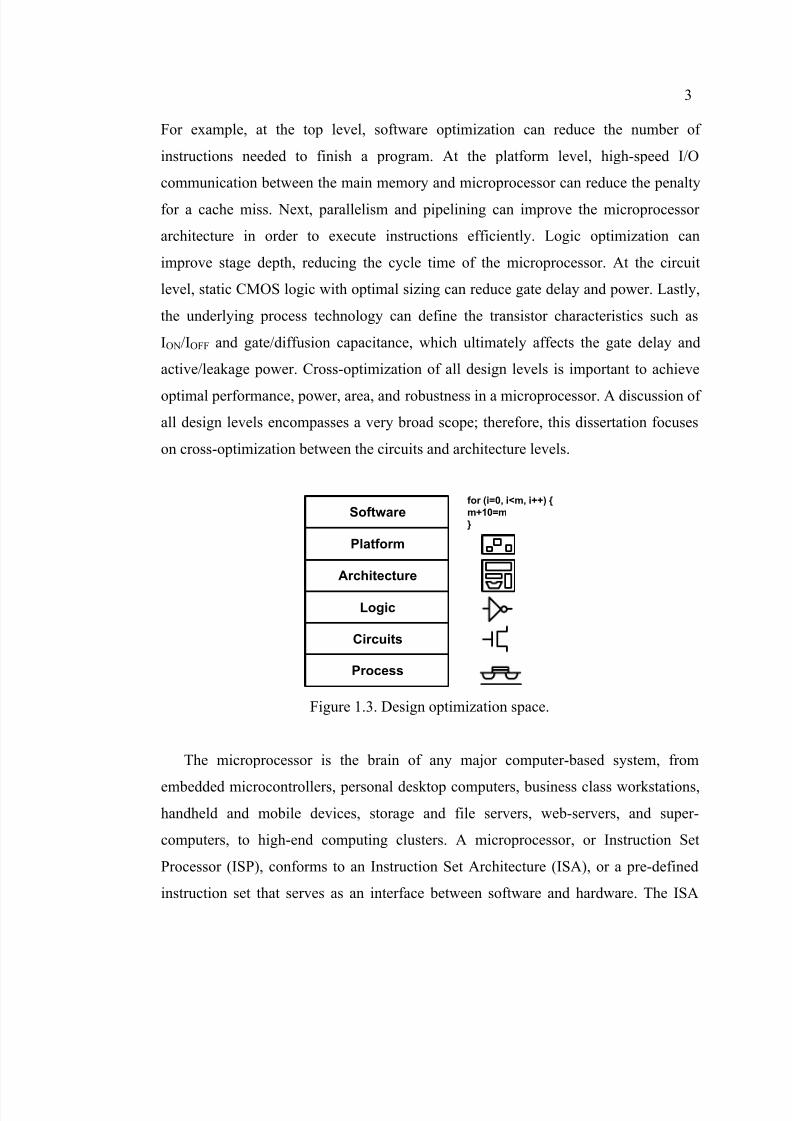
1.2. Microprocessor Overview
The microprocessor optimization space, from top to bottom, includes software,
platform, architecture, logic, circuits, and process (Figure 1.3). All levels have varying
degrees of design optimization space for performance, power, area, and robustness.
8/6/2019 Advanced Micro Architecture and Circuit Design Techniques for on-Chip Memories in CMOS Technology
http://slidepdf.com/reader/full/advanced-micro-architecture-and-circuit-design-techniques-for-on-chip-memories 19/131
8/6/2019 Advanced Micro Architecture and Circuit Design Techniques for on-Chip Memories in CMOS Technology
http://slidepdf.com/reader/full/advanced-micro-architecture-and-circuit-design-techniques-for-on-chip-memories 20/131
4
determines the functionality of a microprocessor and its characteristics. The ISA is
important since it affects the total number of instructions that need to be executed to
finish a program. Instruction-level parallelism (ILP) is the operation of executing
multiple instructions concurrently. A scalar-pipelined microprocessor achieves a form
of ILP, since multiple instructions overlap in the pipeline. This type of microprocessor
results in a maximum theoretical IPC of 1, since it can only fetch one instruction into
the pipeline for every machine cycle. To improve ILP even further, superscalar-
pipelined microprocessors have the ability to fetch and issue multiple instructions for
every machine cycle, improving the IPC to >1. An N-issue wide microprocessor has
the ability to fetch and issue N instructions every machine cycle. Theoretically, an N-
wide machine results in an IPC of N; however, most complex superscalar multi-issue
microprocessors [1.5][1.6] realistically achieve an IPC between 1 to 2.
nCount Instructio IC
Cycle
ns Instructio IPC
N FOT Frequency F
IC
IPC F e Performanc
gatecycle
=
=
×===
×=
)1.1(4
11
As shown in equation 1.1 [1.7], the methods of improving microprocessor
performance include increasing the frequency, improving the number of instructions
executed per clock cycle, and/or reducing the instruction count. If the total executed
instruction count (IC) is reduced, the microprocessor performance should increase
when frequency (F) and instructions per cycle (IPC) remain constant. The frequency
of the microprocessor is defined as the inverse of the cycle time, where the cycle timeis the product of the number of gate delays multiplied by the logic stage depth in a
cycle. A gate delay typically is expressed as a fanout-of-four (FO4) inverter delay --
an inverter that drives a load four times its input capacitance. Logic stage depth is the
total number of gates in the cycle (Ngate). Process technology controls the FO4 delay,
while aggressive logic and circuit design controls the logic stage depth in a cycle [1.8].

8/6/2019 Advanced Micro Architecture and Circuit Design Techniques for on-Chip Memories in CMOS Technology
http://slidepdf.com/reader/full/advanced-micro-architecture-and-circuit-design-techniques-for-on-chip-memories 21/131
5
Aggressive circuit design topologies, such as self-resetting pulsed domino [1.9] and
low-voltage swing differential pass transistor logic [1.10] have found their way into
high-volume shipping microprocessors, reducing the cycle times but at the expense of
added design complexity and power. Improving the process technology and reducing
the logic stage depth in a cycle will increase frequency.
0.11
10
100
1000
10000
100000
1970 1980 1990 2000 2010 2020 Year
M H z 15-30 GHz
8080
8086 386 Pentium®
Pentium® 4
0.11
10
100
1000
10000
100000
1970 1980 1990 2000 2010 2020 Year
M H z
8080
8086 386 Pentium®
Pentium® 4
15-30 GHz
Figure 1.4. Microprocessor frequency trend (courtesy Intel®).
386486
Pentium®
Pentium Pro®
Pentium® II
1989 1993 1997 2001 20051
10
100
L o g i c S t a g e s
Pentium® III
Pentium® 4
386486
Pentium®
Pentium Pro®
Pentium® II
1989 1993 1997 2001 20051
10
100
L o g i c S t a g e s
Pentium® III
Pentium® 4
Figure 1.5. Microprocessor logic depth trend (courtesy Intel®).
Figure 1.4 shows a current trend for processor frequency increasing across time for
various Intel® microprocessors. This plot shows that frequency has doubled everygeneration, assuming the process technology spans every two to three years. Current
microprocessors have a frequency of approximately 4GHz, although the execution
core runs at 8GHz. Figure 1.5 shows that the logic stage depth for the same
microprocessors reduce across time to improve frequency. Current microprocessors
have a logic depth of approximately 8-10 gate stages. Both microprocessor frequency

8/6/2019 Advanced Micro Architecture and Circuit Design Techniques for on-Chip Memories in CMOS Technology
http://slidepdf.com/reader/full/advanced-micro-architecture-and-circuit-design-techniques-for-on-chip-memories 22/131
6
and logic depth have ceilings because of clock skew and jitter overheads [1.11]. There
exists an optimal balance between both frequency and logic depth to improve
performance and power [1.12]-[1.15].
Gate delay is defined by equation 1.2 [1.16] as the product of the output
capacitance C and supply voltage Vdd, divided by the on-current of the device ION.
Reducing output capacitance and/or improving the ION of the gate improves the delay
of the gate. The gate delay equation can be expanded by replacing ION with the alpha-
law model of transistor saturation current [1.17]. From this new equation, a Cox or Vt
reduction in a given process technology, with a channel length of l, will improve the
gate delay. Increasing the width of the transistor at the circuit level improves gate
delay as well.
)2.1(
)(2
α μ Vt Vdd
l
wC
Vdd C
I
Vdd C T
oxON
DELAY
−××
×=
×=
Vdd I Power
I Vdd t t
Power
Vdd C F α Power
Power Power Power Power
OFF LEAKAGE
PEAK
fall rise
IT SHORTCIRCU
ACTIVE
LEAKAGE IT SHORTCIRCU ACTIVE TOTAL
×=
××+
=
×××=
++=
)2
(
)3.1(2
Total power consumption is defined as the sum of active, short-circuit, and leakage
power, as shown in equation 1.3 [1.18]. The active power is the switching component,
where α is the node transition activity factor, F is the clock frequency, and C is the
load capacitance. To lower active power, lowering the supply voltage Vdd is the
strongest knob, because of the square law dependence. The short-circuit power is
directly proportional to I peak (the direct-path current between the supply and ground
while the gate is switching). This short-circuit power occurs when both the PMOS and
NMOS transistors are conducting at the same time, and is dependent on the edge rates

8/6/2019 Advanced Micro Architecture and Circuit Design Techniques for on-Chip Memories in CMOS Technology
http://slidepdf.com/reader/full/advanced-micro-architecture-and-circuit-design-techniques-for-on-chip-memories 23/131
7
trise and tfall. The leakage current component is the product of the off-current (sub-
threshold, gate, etc.) multiplied by the supply voltage. Lowering the supply voltage
Vdd exponentially reduces the leakage power.
0.1
1
10
100
1000
1970 1980 1990 2000 2010 2020
P o w e r ( W a t t s )
1000's of Watts?
8080
8086 386
Pentium®
Pentium® 4
Year
0.1
1
10
100
1000
1970 1980 1990 2000 2010 2020
P o w e r ( W a t t s )
8080
8086 386
Pentium®
Pentium® 4
1000's of Watts?
Year
Figure 1.6. Microprocessor power trend (courtesy Intel®).
1
10
100
1,000
10,000
30 40 50 60 70 80 90 100 110
Temp (°C)
I o f f ( n A / µ m
)0.10 µm
0.13 µm
0.18 µm
0.25 µm
Figure 1.7. Transistor leakage trend (courtesy Intel®).
Lowering Vdd is a powerful method for reducing active and leakage power;
however, it lowers the gate delay and reduces the microprocessor frequency. To
maintain the same gate delay, reducing the device threshold voltage Vt compensates
for lowering Vdd, minimizing the power consumption [1.19][1.20]. The
microprocessor power trend has been increasing at an enormous rate, heading towards
1000’s of watts as shown in Figure 1.6. However, this magnitude of power
consumption is not possible due to the thermal and power limits of current
microprocessors [1.21]. Figure 1.7 shows the leakage trend of a 2-3x increase [1.22]

8/6/2019 Advanced Micro Architecture and Circuit Design Techniques for on-Chip Memories in CMOS Technology
http://slidepdf.com/reader/full/advanced-micro-architecture-and-circuit-design-techniques-for-on-chip-memories 24/131
8
for each technology generation, consuming 30%-50% of the power in the core and
>90% in large caches.
Figure 1.8 shows the trend of total number of transistors in a microprocessor
surpassing one billion transistors on a die. Current shipping high-volume
microprocessors already contain over 1 billion transistors [1.23]. The total number of
transistors is directly proportional to die area in a given technology node. Minimizing
die area is important since it directly affects not only the number of microprocessors
that will fit on a wafer, but also the cost of the part.
0.001
0.01
0.1
1
10100
1000
1970 1980 1990 2000 2010 2020 M i l l i o n T r a n s i s t o r s
1 Billion
Transistors
8080
8086386 Pentium®
Pentium® 4
Year
0.001
0.01
0.1
1
10100
1000
1970 1980 1990 2000 2010 2020 M i l l i o n T r a n s i s t o r s
8080
8086386 Pentium®
Pentium® 4
Year
1 Billion
Transistors
Figure 1.8. Microprocessor total transistor trend (courtesy Intel®).
Figure 1.9. Multi-parameter designs.
Modern microprocessors will expand the use of a multi-parameter design approach
to optimize trade-offs between performance, power, area, and robustness (Figure 1.9).
At the circuit level, existing multi-parameter design techniques include: multi-Vdds,

8/6/2019 Advanced Micro Architecture and Circuit Design Techniques for on-Chip Memories in CMOS Technology
http://slidepdf.com/reader/full/advanced-micro-architecture-and-circuit-design-techniques-for-on-chip-memories 25/131
9
multi-Toxs, multi-Ls, and multi-Vts. The multi-parameter design techniques that exist
in the microarchitecture level include multi-cores and multi-threads. Today, caches
use a separate higher supply voltage and higher channel length transistors from the
core voltage to reduce leakage power, to improve cell stability, and to reduce area.
Multi-threaded and multi-core microprocessors currently are shipping, and deliver
higher performance and lower power than single-thread and single-core counterparts.
The development of additional multi-parameter microarchitecture and circuit level
design techniques will be discussed in this dissertation, and promises to improve the
performance, power, area, and robustness trade-off in microprocessors.
1.3. On-Chip Memory
On-chip memories serve as critical building blocks of high-performance,
superscalar microprocessors. High-end server, desktop, and mobile/handheld
microprocessors introduce new challenges in advanced microarchitecture and circuit
design for on-chip memories in CMOS technology. These new challenges include: (i)
increasing frequencies within the demands of power constraints, (ii) lowering power
consumption for longer battery life and acceptable power density, (iii) reducing area to
improve die cost for multi-core designs, and (iv) combating degradation of dynamic
node robustness which results from increased leakage.
1.3.1. Memory Hierarchy
RF
L1 Cache
L2 Cache
Ln Cache
Main Memory
Execution Units
Size of Memory
Increasing
access time
Figure 1.10. Memory hierarchy.

8/6/2019 Advanced Micro Architecture and Circuit Design Techniques for on-Chip Memories in CMOS Technology
http://slidepdf.com/reader/full/advanced-micro-architecture-and-circuit-design-techniques-for-on-chip-memories 26/131
10
The modern microprocessor contains various types of memories such as caches,
register files (RF), and even content addressable memories (CAM). The register file
communicates directly with the execution units and is on the very top of the memory
hierarchy, requiring very fast access times as shown in Figure 1.10. The register file
communicates results between execution unit computations. The requirement of fast
access times limits the size of the register files, since increasing the area worsens the
delay of the register file. If the data is not located in the register file, the execution
units receive the data from the first level (L1) cache. This L1 cache stores more bits
than the register file; however, the latency is longer. If the data is not located in the L1
cache either, a larger L2 cache access is needed. The L2 cache is larger than the L1
cache in size and has a large access time. Typically in a modern microprocessor, the
register file and L1/L2 caches all reside on-chip, reducing the latency to access them.
If the data is not located in any of these on-chip memories, an access to off-chip main
memory will occur, resulting in a performance penalty.
1. L2 Cache
2. L1 D Cache
3. Trace Cache4. Int. Registers
5. FP Registers
6. Scheduler
7. ROB
8. BTB
9. TLB
SSA
SSA
SSALSA
LSA
CAM/SSA
LSA
SSA
CAM
1 1
2
2
3
4
4
5
6
78
9
11 11
22
22
33
44
44
55
66
7788
99
Figure 1.11. Memory examples in a Pentium® 4 microprocessor.
A memory is implemented using a small signal array (SSA) or large signal array
(LSA). Caches, or SSAs, are implemented with dense 6-transistor memory cells and
differential swing bitlines [1.24][1.25]. Implementation of register files, or LSAs,
include single-ended read/write bitlines to reduce area, especially for multi-ported

8/6/2019 Advanced Micro Architecture and Circuit Design Techniques for on-Chip Memories in CMOS Technology
http://slidepdf.com/reader/full/advanced-micro-architecture-and-circuit-design-techniques-for-on-chip-memories 27/131
11
arrays. Content addressable memory is addressed using a key that is compared with
the data stored in the memory, to determine a match. Figure 1.11 shows a Pentium® 4
microprocessor [1.26] and the locations of key memory components. The L2 cache,
L1 data cache, trace cache, scheduler, and branch table buffer are implemented using
SSAs. The integer register file, floating-point register file, and re-order buffer are
implemented using LSAs. The scheduler and table look-up buffer are implemented
with CAMs. These memories consume a large portion of the die. They contribute to a
large portion of the overall power, and careful design of these blocks is necessary to
improve performance, lower power, reduce area, and increase robustness.
1.3.2. Register Files
Multi-ported register files are basic building blocks in superscalar microprocessors
since they enable concurrent execution of multiple instructions during one cycle. The
architecture of the register file consists of a decode block and array block (Figure
1.12). The size of the register file varies depending on the number of entries, bits, and
read/write ports. Since the number of read/write ports vary, there is a separate decode
block to determine the specific location corresponding to the input address. A
read/write N-wide address bit scales to a maximum of 2 N
number of entries and stores
M-wide data for each entry. Therefore, the total number of bits stored would MxN.
D e c o d e r
Figure 1.12. Register file architecture.

8/6/2019 Advanced Micro Architecture and Circuit Design Techniques for on-Chip Memories in CMOS Technology
http://slidepdf.com/reader/full/advanced-micro-architecture-and-circuit-design-techniques-for-on-chip-memories 28/131
12
Register files with few ports can employ differential bitlines to read from the
memory cell, but must incorporate sense-amplifiers into the design [1.27]-[1.29].
Obviously, differential bitlines for highly multi-ported memories are problematic due
to the wiring congestion. To improve speed, single-ended sensing methods have been
proposed [1.30]-[1.33]; however, most modern register files use large-signal, single-
ended implementations with fully time-borrowable domino logic [1.34]-[1.37].
The decoder selects the accessed entry in the register file that corresponds to the
input address. Figure 1.13(a) shows the logical representation of the decoder as a wide
AND gate that produces the row select enable. Figure 1.13(b) shows the physical
design implementation of the wide AND gate. Actual implementation is done in
multiple states with predecoders to reduce routing and increase the amount of sharing
in a decoder. This allows significant sharing across each row select decode logic, since
there is no duplication. Predecoding often improves performance since the total
switched capacitance is reduced.
Figure 1.13. (a) Logical decoder (b) Physical implementation.
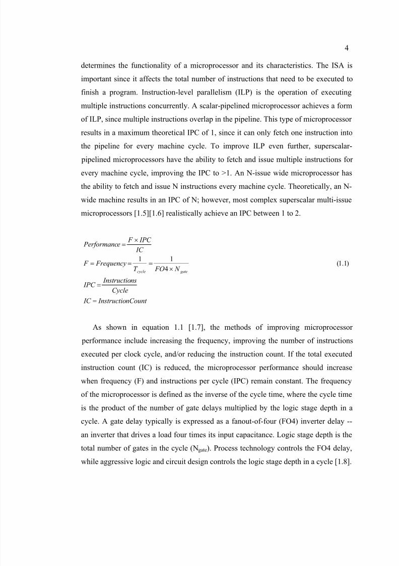
The array circuits include the memory cell and read/write ports. Figure 1.14 shows
an example x-read and y-write register file bit cell with single-rail reads and writes,
where x and y are the number of read and write ports, respectively. Cross-coupled
inverter and write pass transistors sizing determines optimal write stability and state
retention for low voltages. A stack of 2 transistors form a read port that is part of a
wide domino NAND-NOR gate. The top NMOS transistor in the stack is called the
8/6/2019 Advanced Micro Architecture and Circuit Design Techniques for on-Chip Memories in CMOS Technology
http://slidepdf.com/reader/full/advanced-micro-architecture-and-circuit-design-techniques-for-on-chip-memories 29/131
13
read access device, while the bottom NMOS transistor is the data device. Since reads
are buffered, there is no read stability issue, unlike 6-transistor memory cells used in
SSAs.
Figure 1.14. Multi-ported x-read y-write register file cell.
rd_clk
rd_en
wr_enwr_clk
wrwl
rdwl
l b l
g b l
rdout
w r b l
d a t a i n
“0”
lblpre_enlbl_clk
lblpre
gblpre_engbl_clk
gblpre
keeper
keeper
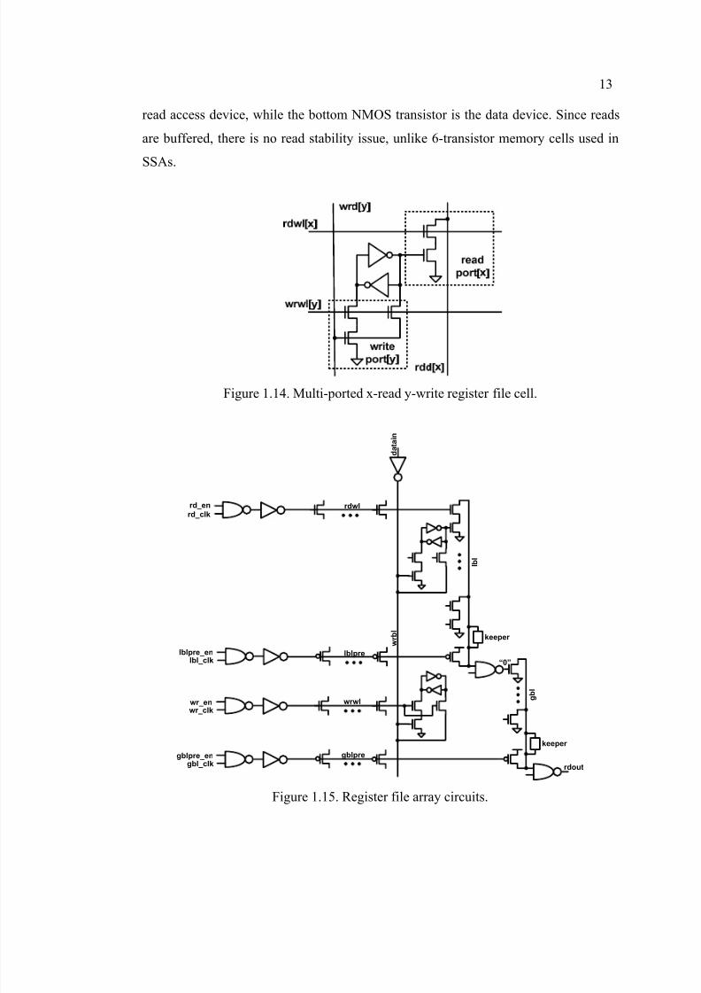
Figure 1.15. Register file array circuits.

8/6/2019 Advanced Micro Architecture and Circuit Design Techniques for on-Chip Memories in CMOS Technology
http://slidepdf.com/reader/full/advanced-micro-architecture-and-circuit-design-techniques-for-on-chip-memories 30/131
14
Figure 1.15 shows the entire array with read and write circuits and loads. Each cell
has separate read wordlines (rdwl) and write wordlines (wrwl). Both are generated
from different read and write decoders. The read port outputs for a domino wired-OR
are typically routed in metal2. The pre-charge, keeper, and NAND circuitry are
located at the end of the bitline and is part of the merge area. Segmentation varies in
width, but typically is a 4, 8, or 16-wide domino gate and forms a local bitline (lbl). To
merge two local bitlines together, a simple NAND gate is used. Since only one bitline
is active and the other bitline remains at Vdd, the NAND gate performs the logic
operation of an inverter. This NAND merge drives into the global bitline (gbl)
pulldown. The global bitline pulldown is a second level of wired-OR and completes
the merging of all entries. Typically, the global bitlines are very long and therefore are
routed in a less resistive metal4. Writes are accomplished via a static write data bitline
(wrbl) using NMOS-only write ports.
With CMOS technology scaling, aggressively low threshold devices result in an
exponential increase in bitline active leakage currents and poor bitline noise immunity
[1.38]. Figure 1.16 shows the impact of increased leakage on the robustness of wide
dynamic-OR gates such as an 8-wide local bitline. Increased keeper sizes are
necessary to maintain adequate noise margins and burn-in functionality; however, thiscomes at a cost of bitline delay increase due to keeper contention. Scaling has forced
designers to reduce the segmentation. This combats the increase in leakage, but
increases the area because area efficiency reduces as segmentation decreases.
Figure 1.16. Local bitline with increased keeper size due to leakage.

8/6/2019 Advanced Micro Architecture and Circuit Design Techniques for on-Chip Memories in CMOS Technology
http://slidepdf.com/reader/full/advanced-micro-architecture-and-circuit-design-techniques-for-on-chip-memories 31/131
15
1.4. Thesis Contribution and Organization
This thesis proposes microarchitecture and circuit techniques that aim to improve
the trade-offs between performance, power, area, and robustness for on-chip
memories. These techniques address the improvement of one of the most important
on-chip memories in a superscalar microprocessor -- large-signal multi-ported register
files.
Large-signal multi-ported register files contain the most critical speed paths,
limiting the microprocessor frequency and consuming one of the largest percentages
of power at ~25%. A large variety of register files in a state-of-the-art microprocessor
consumes a significant amount of area, resulting in some of the hottest spots,
especially near the execution core. As technology scales, increased leakage degrades
the robustness of dynamic circuits, requiring increased keeper sizes in register file
local/global bitlines to maintain functionality. The scalability of the register file is a
concern in modern microprocessors. As microprocessors become wider to exploit
instruction level parallelism, this increases the amount of read/write ports. Increasing
the read/write ports results in a quadratic growth in register file area, impeding the
increase in microprocessor frequency. Pipelined register files enable high frequencies
at the cost of extra clock power and increased latency. As instruction window sizecontinues to expand in modern microprocessors, the resulting demand for additional
register file entries requires increased use of wide-OR dynamic circuits. However,
these circuits, found primarily in local/global bitlines, are susceptible to leakage noise.
The goal of the proposed work is to address the performance, power, area, and
robustness challenges of the modern register file. The proposed techniques in this
dissertation will address the disadvantages of previous published techniques, and will
provide solutions to these new challenges.
Chapters 2 through 5 deal with improving performance, lowering power, reducing
area, and/or improving the robustness of register files. Improving the performance of a
microprocessor is accomplished by either increasing the frequency and/or increasing
the number of instructions executed per cycle. New techniques need to lower active
and leakage power since today’s microprocessors are power constrained. Further
8/6/2019 Advanced Micro Architecture and Circuit Design Techniques for on-Chip Memories in CMOS Technology
http://slidepdf.com/reader/full/advanced-micro-architecture-and-circuit-design-techniques-for-on-chip-memories 32/131
16
integration and the trend towards multiple cores on a die will impact the cost of the
microprocessor; therefore, the area of the register file is important. As technology
scales and threshold voltage decreases, the register file robustness against leakage
variations also are critical.
Chapter 2 compares and contrasts multi-banking, multi-frequency, and multi-bit
width register files to reduce power and lower area. Comparisons of integer register
files for 4-wide to 8-wide issue machines in 65nm CMOS show that using both multi-
banking and multi-frequency techniques show good promise in reducing area,
improving frequency, and lowering active and leakage power for future multi-ported
register files in wide-issue machines. To aid in comparison, an area, frequency, and
power (active and leakage) model for multi-ported register files is developed using
technology and architectural parameters.
Chapter 3 explains the concept of physical locality and introduces multi-access
register files to improve the performance of the processor. This chapter proposes a
circuit solution to enable variable latency arrays, depending on the physical locality.
This improves the latency of loops with dependent instructions. Furthermore, this
chapter proposes a method of re-configuring the address decoding to take better
advantage of asymmetric access times for the physical register file. The proposedscheme achieves a significant recovery of the IPC lost. Multi-cycle access memories
with variable latency show good scaling trend as the microprocessor’s pipeline is
further deepened.
Chapter 4 describes the use of multi-threshold devices to improve robustness of a
register file in the face of increasing leakage currents as technology scales. A leakage-
tolerant self reverse-bias bitline technique is described; the technique establishes
negative gate-source under-drive on the leakage-limiting low-VTH access transistors.
This is achieved without distributing additional supply/bias voltages, pre-conditioning
control signals, or gate-oxide overstress. This technique shows good promise for
improving delay-robustness trade-offs in future scaled technologies using leaky low-
VTH devices. Delay improvement is achieved by reduced keeper contention, and
robustness improvement results from the use of negative gate-source under-drive.

8/6/2019 Advanced Micro Architecture and Circuit Design Techniques for on-Chip Memories in CMOS Technology
http://slidepdf.com/reader/full/advanced-micro-architecture-and-circuit-design-techniques-for-on-chip-memories 33/131
17
Chapter 5 describes an example of a variation-tolerant register file with a multi-
keeper, and describes several other low-power/noise-tolerant techniques in 65nm
CMOS. Significant process, supply voltage, and temperature (PVT) induced variations
in transistor leakage limit the performance and robustness of wide dynamic register
file bitlines. The low-power/noise-tolerant techniques include the following: fused
static decode and array read, split decoder with PVT/burn-in compensation, leakage-
tolerant split wordline architecture, and shared twin memory cell topology.
Chapter 6 describes the main contributions of the thesis, summarizes the various
techniques described in the thesis, and highlights the possible areas of future work in
register file design.

8/6/2019 Advanced Micro Architecture and Circuit Design Techniques for on-Chip Memories in CMOS Technology
http://slidepdf.com/reader/full/advanced-micro-architecture-and-circuit-design-techniques-for-on-chip-memories 34/131
18
References
[1.1] J. Bardeen and W. H. Brattain, “The transistor, a semi-conductor transistor,” Physics Review, vol. 74, pp. 230-231, July 1948.
[1.2] Intel® Corporation, MCS-4 Micro Computer Set, pp. 1-12.
[1.3] G. Moore, “Cramming more components onto integrated circuits,” Electronics,
vol. 38, pp. 114 -117, April 1965.
[1.4] P. Bai, et al., “A 65nm logic technology featuring 35nm gate lengths, enhancechannel strain, 8 Cu interconnect layers, low-k ILD and 0.57um
2SRAM cell,”
in International Electron Devices Meeting Technical Digest , Dec. 2004, pp.
657-660.
[1.5] G.S. Sohi, et al., “Multiscalar processors,” in Proceedings 22th
International Symposium Computer Architecture, June 1995, pp. 414-425.
[1.6] S. Palacharla, et al., “Complexity-effective superscalar processors,” in Proceedings 24
thInternational Symposium Computer Architecture, June 1997,
pp. 206-218.
[1.7] J. Hennessy and H. Patterson, Computer Architecture: a Quantitative
Approach, Morgan Kaufmann, 1990.
[1.8] M. Horowitz, “Clocking strategies in high performance processors,” in
Symposium VLSI Circuits Digest Technical Papers, June 1992, pp. 50-53.
[1.9] G. Hinton, et al., “A 0.18-μm CMOS IA-32 processor with a 4-GHz integer
execution unit,” IEEE Journal Solid-State Circuits, vol. 36, pp. 1617-1627, Nov. 2001.
[1.10] D. Deleganes, et al., “Low-voltage swing logic circuits for a Pentium® 4
processor integer core,” IEEE Journal Solid-State Circuits, vol. 40, pp. 36-43,Jan. 2005.
[1.11] D. Harris and M. Horowitz, “Skew-Tolerant Domino Circuits,” IEEE Journal
Solid-State Circuits, vol. 32, pp. 1702-1711, Nov. 1997.
[1.12] V. Agarwal, et al., “Clock rate versus IPC: the end of the road for conventionalmicroarchitectures,” in Proceedings 27
thInternational Symposium Computer
Architecture, May 2000, pp. 248-259.

8/6/2019 Advanced Micro Architecture and Circuit Design Techniques for on-Chip Memories in CMOS Technology
http://slidepdf.com/reader/full/advanced-micro-architecture-and-circuit-design-techniques-for-on-chip-memories 35/131

8/6/2019 Advanced Micro Architecture and Circuit Design Techniques for on-Chip Memories in CMOS Technology
http://slidepdf.com/reader/full/advanced-micro-architecture-and-circuit-design-techniques-for-on-chip-memories 36/131
20
[1.25] B. Amrutur and M. Horowitz, “Speed and power scaling of SRAM’s,” IEEE Journal Solid-State Circuits, vol. 35, pp. 175-185, Feb. 2000.
[1.26] S. Wijeratne, et al., “A 9GHz 65nm Intel Pentium® 4 Processor Integer
Execution Core,” in International Solid-State Circuits Conference Digest Technical Papers, Feb. 2006, pp. 110-111.
[1.27] M. Golden and H. Partovi, “A 500MHz, write-bypassed, 88-entry, 90-bit
register file,” in Symposium VLSI Circuits Digest Technical Papers, June1999, pp. 105-108.
[1.28] L. Lev, et al., “A 64-b microprocessor with multimedia support,” IEEE
Journal Solid-State Circuits, vol. 30, pp. 1227-1238, Nov. 1995.
[1.29] R. Heald, et al., “A third-generation SPARC v9 64-b microprocessor,” IEEE
Journal Solid-State Circuits, vol. 35, pp. 1526-1538, Nov. 2000.
[1.30] H. Hara, et al., “0.5-μm 3.3-V BiCMOS standard cells with 32-kilobyte cache
and ten-port register file,” IEEE Journal Solid-State Circuits, vol. 27, pp.1579-1584, Nov. 1992.
[1.31] C. Asato, “A 14-port 3.8-ns 116-word 64-b read-renaming register file,” IEEE
Journal Solid-State Circuits, vol. 30, pp. 1254-1258, Nov. 1995.
[1.32] R. Jolly, “A 9-ns, 1.4-gigabyte/s, 17-ported CMOS register file,” IEEE Journal
Solid-State Circuits, vol. 26, pp. 1407-1412, Oct. 1991.
[1.33] N. Tzartzanis and W. Walker, “A differential current-mode sensing method for high-noise-immunity, single-ended register files,” in International Solid-State
Circuits Conference Digest Technical Papers, Feb. 2004, pp. 506-507.
[1.34] R. Joshi and W. Hwang, “Design considerations and implementations of a high
performance dynamic register file,” in Proceedings 12th
International Conference on VLSI Design, Jan. 1999, pp. 526-531.
[1.35] W. Hwang, et al., “A 500-MHz, 320-word x 64-bit, eight-port self-resetting
CMOS register file,” IEEE Journal Solid-State Circuits, vol. 34, pp. 56-67,
Jan. 1999.
[1.36] R. Joshi, et al., “Implementation of a high speed multiport register file in a
1.8V, 0.25µm CMOS bulk and SOI technology,” in Proceedings International
Symposium VLSI Technology Systems Applications, June 1999, pp. 274-277.

8/6/2019 Advanced Micro Architecture and Circuit Design Techniques for on-Chip Memories in CMOS Technology
http://slidepdf.com/reader/full/advanced-micro-architecture-and-circuit-design-techniques-for-on-chip-memories 37/131
21
[1.37] N. Tzartzanis, et al., “A 34 word×64 b 10 R/6 W write-through self timed dual-
supply-voltage register file,” in International Solid-State Circuits Conference
Digest Technical Papers, Feb. 2002, pp. 416-417.
[1.38] R. Krishnamurthy, et al., “A 130-nm 6-GHz 256x32b leakage-tolerant register file,” IEEE Journal of Solid-State Circuits, vol. 37, pp. 624-632, May 2002.

8/6/2019 Advanced Micro Architecture and Circuit Design Techniques for on-Chip Memories in CMOS Technology
http://slidepdf.com/reader/full/advanced-micro-architecture-and-circuit-design-techniques-for-on-chip-memories 38/131
22
REGMOD: A MULTI-PORTED REGISTER FILE MODEL FOR
SUPERSCALAR MICROPROCESSORS
Steven K. Hsu, Chris Wilkerson, Ram K. Krishnamurthy, and Shih-Lien Lu
To be submitted to the 39th
International Symposium on Microarchitecture
MICRO-39, 2006.

8/6/2019 Advanced Micro Architecture and Circuit Design Techniques for on-Chip Memories in CMOS Technology
http://slidepdf.com/reader/full/advanced-micro-architecture-and-circuit-design-techniques-for-on-chip-memories 39/131
23
2. MULTI-BANKING, FREQUENCY, AND BIT-WIDTH
REGISTER FILES
2.1. Introduction
Register files are critical building blocks in state-of-the-art, superscalar wide-issue
microprocessors. There are many highly ported register file structures, such as the
integer and floating-point register file, re-order buffer, reservation station, and register
alias table in a microprocessor. As microprocessors become wider to exploit
instruction level parallelism, the scalability of multi-ported register files is a concern,
since it requires more read/write ports. These multi-ported register files occupy large
portions of microprocessor die area, since the area is quadratic with the number of
read/write ports. Large register files contain long wordline and bitline wires, which
aggravate critical microprocessor speed paths. Moreover, longer wire has larger
interconnect and transistor capacitance and increases register file power consumption,
which in turn plays a large role in microprocessor thermal power density limits.
Register files consume one of the largest percentages of power in a microprocessor
(~25%). Design parameters such as the number of read/write ports, bits, and entries
contribute to register file area, frequency, and power. Therefore, understanding these
register file trade-offs is critical in the design process, and an accurate model is
necessary for analysis. Various techniques impact these trade-offs differently and this
chapter will present REGMOD, a register file model, to show trade-offs of each
technique.
This chapter describes a model that estimates register file area, frequency, and
power using technology and design parameters. Physical design based technology
parameters include FO4 delay, metal layer resistance, capacitance, and layout pitch.
By using the interconnect pitch, the memory cell dimensions and total register file area
are estimated. PMOS/NMOS transistor gate and diffusion capacitance per micron and
the interconnect resistance and capacitance contribute to estimating the delay and
active power. The sub-threshold leakage current per micron of un-stacked and stacked
transistors contribute to estimating the leakage power. Total leakage power is

8/6/2019 Advanced Micro Architecture and Circuit Design Techniques for on-Chip Memories in CMOS Technology
http://slidepdf.com/reader/full/advanced-micro-architecture-and-circuit-design-techniques-for-on-chip-memories 40/131
24
determined by multiplying the sub-threshold leakage current per micron with the total
PMOS/NMOS leaking transistor width. Design parameters include the number of
entries, bits, segmentation, read/write ports. Increasing the number of entries, bits, and
read/write ports increases the area, frequency, and power. Increasing segmentation
lowers register file area since more cells are merged with a single gate. This circuit
technology and design parameter based model allows optimal analysis of different
register file implementations brought about by microarchitecture definition.
Using REGMOD, various microarchitecture and circuit techniques show promise
in improving performance, lowering power and reducing area. Lowering power is
important in today’s power constrained microprocessor designs where the highest
frequency is determined by a power envelope and not the maximum allowed voltage.
This chapter concentrates on the integer register file, one of the largest, most speed
critical, and power hungry multi-ported register file in today’s microprocessor. In fact,
one of the hottest spots on a microprocessor during a high-power test is the integer
execution unit due to simultaneous register file read/write operations. By keeping the
performance constant, comparisons of power and area trade-offs become clearer.
Performance remains constant by fixing the throughput of each register file design.
Therefore, the instructions per cycle of the microprocessor remain constant for comparisons of the different register file configurations, and the overall
microprocessor performance remains unaffected. The first comparison explores two
techniques, multi-banking (duplication) and multi-frequency (double throughput), and
shows the trade-offs of each register file design. Multi-banking and multi-frequency
techniques, separately and in combination, show power and area savings at constant
performance. Lastly, multi-bit width register files reduce the active read/write power,
by clock and wordline gating of narrow bit-width data values.
2.2. Area, Frequency, Power Model
It is important for a model to capture all three aspects of design: area, frequency,
and power, to help compare the interactions of each design vector. The previously
published CACTI [2.1] is an area, frequency, and power model widely used

8/6/2019 Advanced Micro Architecture and Circuit Design Techniques for on-Chip Memories in CMOS Technology
http://slidepdf.com/reader/full/advanced-micro-architecture-and-circuit-design-techniques-for-on-chip-memories 41/131
25
throughout the community and initially meant for differential small-signal bitline
design used in caches. Extensions to CACTI allow multi-port usage analysis; however,
the circuits used in multi-ported register file designs are typically not small-signal. The
large-signal designs employ single rail bitlines to reduce routing congestion.
Therefore, CACTI model represents the delay and power of a non-typical register file
design. ESTIMA [2.2] is another previously published register file estimator that
accurately models area through curve fitting, and uses switch level active power
estimation. The main disadvantage of this model is that it does not account for leakage
power. The published Zyban [2.3], Ghose [2.4], and Zhao [2.5] power models leave
the leakage component out as well. As technology scales, leakage power increases due
to the decrease in threshold voltages. Estimating leakage power is especially important
in low-activity register files, where the leakage is already a large component of overall
register file power. Typically, leakage accounts for as much as 30% of the total
register file power in today’s design. Therefore, it is crucial that new register file
power models capture this component.
2.2.1. Area Model
The area of the register file affects the cost, frequency, and power of the processor.
The memory cell size is the largest contributor to total register file area. It determines
the length of interconnect wires in the register file, such as the wordlines and bitlines.
These interconnect wires add capacitance to each node, requiring the total power
consumption to account for the extra capacitance. Devices with increased sizes drive
these long interconnect wires, which in turn affect the delay of the register file. The
interconnect wires have resistive and capacitive components; therefore, it adds to the
overall delay.
The area of a register file has two components: array and decoder. The array area
is composed of the memory cells (cross-coupled inverters and read/write port
transistors) and peripheral circuits (merge NAND, global bitline circuits, pre-
charge/keeper devices, and write data drivers). Cross-coupled inverters store a single
memory bit. Multiple read/write ports attach to the memory bit to allow simultaneous

8/6/2019 Advanced Micro Architecture and Circuit Design Techniques for on-Chip Memories in CMOS Technology
http://slidepdf.com/reader/full/advanced-micro-architecture-and-circuit-design-techniques-for-on-chip-memories 42/131
26
read/write operations. The peripheral circuits are used to read data out of and write
data in to the register file. Decoder area includes the read/write pre-decoders, local
decoders, wordline drivers, and clocking circuits/drivers. Area efficiency is calculated
by dividing the array area by the total area. Designs attain high area efficiency by
reducing the amount of merge and decoder logic.
Cell area is estimated by the number of read/write ports. In a single-rail register
file design, there is one wordline and one bitline track for each read or write port.
Most register files in modern microprocessors employ single-rail bitlines and
wordlines to reduce area. Additional tracks are allocated for power/ground wires in the
memory cell. These additional tracks are not minimum in width and are modeled with
a factor β (>1) to decrease the wire resistance and to provide a good power/ground
grid. The X dimension of the memory cell is the number of read/write ports plus the
power tracks, multiplied by the minimum pitch of metal4. The Y dimension of the
memory cell is the number of read/write ports plus the power tracks, multiplied by the
minimum pitch of metal3 as depicted in Figure 2.1. Equation (2.1) summarizes the
above discussion and shows that a register file cell area is proportional to the square of
the number of ports.
Figure 2.1. Multi-ported memory cell layout.
)()#(
)1.2(Re#
Re
3
4
entriesCell AreabitsCell Area Area
#Power)#Writead ( PitchCell
#Power)#Writead (# PitchCell
ymerge xdecoder TOTAL
M Y
M X
×××××=
×++=
×++=
β
β

8/6/2019 Advanced Micro Architecture and Circuit Design Techniques for on-Chip Memories in CMOS Technology
http://slidepdf.com/reader/full/advanced-micro-architecture-and-circuit-design-techniques-for-on-chip-memories 43/131
27
Estimated peripheral circuit area is a percentage (~30-40%) of the vertical
dimension of a bundle of memory cells. The vertical dimension of the register file is
the number of entries multiplied by the height of a single memory cell, plus the total
peripheral vertical dimension. The total horizontal array dimension is the number bits
multiplied by the width of a single memory cell. A bundle is a group of memory cells
that form a local bitline for each read port. Often, the bundles are composed of 4, 8,
16-way local bitlines. Leakage and noise concerns sometimes force designers to
reduce the number of cells in a bundle to maintain functionality. However, this
decreases the area efficiency since more merge circuitry is required. The estimated
horizontal dimension of the decoder is a percentage (~30-40%) of the array width. The
estimated vertical dimension is pitch matched to memory cell and merge circuitry
height. Figure 2.2 shows that area increases as the number of ports increase for 64,
128, and 256 entry register files. A port ratio of 2:1 represents 2 read ports for 1 write
port. For example, 6 ports represent 4 read ports and 2 write ports.
0.0
5.0
10.0
15.0
20.0
25.0
30.035.0
40.0
45.0
6 12 18 24
Ports (2R:1W ratio)
A r e a
64 entries
128 entries
256 entries
Figure 2.2. Register file area across entries and ports.

8/6/2019 Advanced Micro Architecture and Circuit Design Techniques for on-Chip Memories in CMOS Technology
http://slidepdf.com/reader/full/advanced-micro-architecture-and-circuit-design-techniques-for-on-chip-memories 44/131
28
2.2.2. Frequency Model
Register file latency consists of the decoder and array read delay. The frequency of
the register file is determined by calculating the inverse of the cycle time. The cycle
time includes the gate delay, interconnect delay, and clock margin components.
REGMOD individually estimates each transistor size in the critical path, allowing a
certain stage effort for each gate. The stage effort, or logical effort of the gate, is the
fan-out divided by the fan-in. Each gate delay in the critical path is linearly
proportional to an FO4 gate delay. Single-cycle register file latency incorporates gate
delay through the decoder and array as part of the cycle time. Pipelined register files
enable high operating frequencies with multi-cycle read/write accesses. Two-cycle
register file latency allows address decoding to occur in the first cycle, while in the
second cycle the array read occurs. For these higher frequency designs, higher effort
per stage is required, increasing the average gate size in the array. In lower, single-
cycle frequency designs, the lower effort per stage allows reduced average gate size.
The clocking margin is caused by the static-to-domino interface between the
decoder and array. The decoder of the register file is implemented using conventional
static CMOS logic and the wordline driver converts the decoder output into a domino
compatible signal before it enters the array. This static-to-domino interface has a clock margin tax of FO4 delay multiplied by a factor δ (>1) as part of the cycle time. Setup
time is necessary since any clock skew or jitter may cause incorrect entry access.
Interconnect delay contribution is caused by long pre-decoder lines, wordlines, and
bitlines and is calculated by multiplying the RC time constant by 0.69. The wire
resistance multiplied by the wire capacitance produces the RC time constant. Since
each metal has different resistive and capacitive properties, different resistance and
capacitance per micron values are used for different metal layers. A summary of the
frequency model is shown in Equation (2.2), while Figure 2.3 shows that frequency
decrease as the number of ports increase across 64, 128, and 256 entries.

8/6/2019 Advanced Micro Architecture and Circuit Design Techniques for on-Chip Memories in CMOS Technology
http://slidepdf.com/reader/full/advanced-micro-architecture-and-circuit-design-techniques-for-on-chip-memories 45/131
29
RC ct Interconne
FOClock
FO FO FO FO FO FO FO Decode
FO FO FO FO FO FO FO Array
Decode ArrayMAX Gates Decode ArraySUM Gates
Clock ct InterconneGatesCycleTime
CycleTime Frequency
no finna fininv prena preinvaddbinvadd
na gbl gbl nalbl lbl invwl nawl
cycle
cycle
×=
×=
++++×=
+++++×=
==
++=
=
+
69.0
4
4
)(4
4
)(4
)2.2(),(),(
1
2 _ 2 _ _ 2 _ _ _
2 _ 2 _ _ 2 _
2
1
δ
0.0
0.2
0.4
0.6
0.8
1.0
1.2
6 12 18 24
Ports (2R:1W ratio)
F r e q u e n c y
64 entries
128 entries
256 entries
Figure 2.3. Register file frequency across entries and ports.
2.2.3. Power Model
The power consumption model divides power into two main categories: active and
leakage. Equation (2.3) shows the model for the active and leakage power. The active
power is quadratically related to the supply voltage and increases linearly with
frequency and capacitance. Active power is scaled by the activity factor. The data bias
determines the activity factor for domino gates. The leakage power is determined by
the sub-threshold current and supply voltage. The total sub-threshold leakage is

8/6/2019 Advanced Micro Architecture and Circuit Design Techniques for on-Chip Memories in CMOS Technology
http://slidepdf.com/reader/full/advanced-micro-architecture-and-circuit-design-techniques-for-on-chip-memories 46/131
30
calculated by multiplying the sub-threshold leakage current per micron (either PMOS
or NMOS) by the leaking transistor width. Data bias also is important for leakage
calculation since it determines whether a PMOS or NMOS is leaking. The short-circuit
power is dependent upon the supply voltage and threshold voltage of the technology,
delay, and edge-rate of the signals. For simplicity’s sake, this register file model has
omitted the short-circuit power. Typically, the short-circuit power accounts for less
than 15% of the overall power.
Vdd I Power
Vdd C F α Power
Power Power Power
leakagethreshold sub LEAKAGE
ACTIVE
LEAKAGE ACTIVE TOTAL
×=
×××=
+=
− _
2 )3.2(
The active power of the register file is the sum of the read/write power
components. The active read power is composed of the decoder, wordline, read clock,
and bitline power. The sum of the read decoder, read wordline, and read clock power
is multiplied by the number of active read ports, while the bitline components are
multiplied by the total number of bits and active read ports. The active power of a “0”
read is comprised of only the decoder, wordline, and read clock power, since the
domino bitlines consume no active power during “0” reads. The sum of the write
decoder and write wordline is multiplied by the number of active write ports, while the
sum of the write data and cell power is multiplied by the total number of bits and
active write ports. Assuming the read domino local and global bitlines discharge
during a “1” read operation, the active power will be much higher for reading all “1”s
than reading all “0”s. Equation (2.4) shows a summary of the active power calculation.
)##(
#)(
)4.2()##)(
#)(
_ _ _
_ _ _
writebits P P
write P P P
read bits P P P P
read P P P Power
cell data
clock writewordlinewritedecoder write
sdl gbl nand lbl
clock read wordlineread decoder read ACTIVE
××++
×+++
××++++
×++=

8/6/2019 Advanced Micro Architecture and Circuit Design Techniques for on-Chip Memories in CMOS Technology
http://slidepdf.com/reader/full/advanced-micro-architecture-and-circuit-design-techniques-for-on-chip-memories 47/131
31
Modeling leakage power is important as technology scales [2.6]. The leakage
power equals the sub-threshold current multiplied by the supply voltage. However, the
leakage current is composed of many smaller components, such as the wordline,
bitcell, read/write ports, NAND merge circuitry, global merge circuitry, latches, and
read/write decoder logic. The wordline leakage is a product of the number of entries,
and read/write ports. In this case, since the wordline drivers for read and write are
different, the read wordline leakage and write wordline leakage will be different.
Leakage is calculated for the steady-state bias conditions of each gate. For example, a
wordline driver inverter outputs a “0”; therefore, the NMOS device is on and the
PMOS device is off and leaking. Stack leakage is used to determine the leakage
through stacked devices. Long channel optimization throughout the register file
minimizes leakage current in the register file [2.7], reducing individual transistor
leakage by approximately 3x [2.8]. A summary of the leakage power calculation is
shown in Equation (2.5). Figure 2.4 shows power increasing as the number of ports
increase across 64, 128, and 256 entries.
Vdd writeread I
read bits I
read pulldowns
entriesbits I
read pulldowns
entriesbits I
writeentriesbits I
read entriesbits I
entriesbits I
writeentries I
read entries I
Vdd I Power
leakagedecoder
leakage sdl
leakage global
leakagenand
leakagewrite
leakageread
leakagebitcell
leakagewrwl
leakagerdwl
Leakage LEAKAGE
×××+
××+
×××+
×××+
×××+
×××+
××+
××+
××=
×=
)]##(
)##(
)##
##(
)##
##(
)5.2()###(
)###(
)##(
)##(
)##[(
_
_
_
_
_
_
_
_
_

8/6/2019 Advanced Micro Architecture and Circuit Design Techniques for on-Chip Memories in CMOS Technology
http://slidepdf.com/reader/full/advanced-micro-architecture-and-circuit-design-techniques-for-on-chip-memories 48/131
32
0.0
5.0
10.0
15.0
20.0
25.0
30.0
35.0
40.0
45.0
50.0
6 12 18 24
Ports (2R:1W ratio)
P o w e r
64 entries
128 entries
256 entries
Figure 2.4. Register file power across entries and ports.
Figure 2.5. Array steady state leakage estimation.

8/6/2019 Advanced Micro Architecture and Circuit Design Techniques for on-Chip Memories in CMOS Technology
http://slidepdf.com/reader/full/advanced-micro-architecture-and-circuit-design-techniques-for-on-chip-memories 49/131
33
Figure 2.5 shows a register file circuit diagram of the array read/write path with
appropriate steady-state data bias. The data bias of each node in the register file is
important since it determines which actual transistors are leaking. In the example, an
un-accessed read wordline (rdwl) inverter has a steady-state data bias output condition
of “0”, while the input is “1”. Since the input is “1”, the NMOS device is turned on,
while the PMOS device is turned off. Therefore, the PMOS transistor width is the
leakable transistor width, and is multiplied by the PMOS leakage current per micron to
determine the leakage current of the inverter.
2.3. Model Accuracy Verification
The model accuracy is verified for a class of representative register files ranging inentries, bits, and ports from a 65nm CMOS microprocessor. These register files
includes a mix of high and low number of entries (32 to 144), bits (64 to 512), and
ports (2 to 9) to show a good accuracy range for different configurations. The
quantitative values for delay, area, and power are especially important, however, the
relative difference between register file configurations gives a good estimation of
improvement or degradation for comparing techniques. At an operation frequency of
4GHz, the average absolute error in area is 7% (maximum 8%) versus actually
physical VLSI implementation. Average absolute error in total power is 23%
(maximum 30%) versus a switch level simulator power estimator.
2.4. Area and Power Reduction using Multi-Banking and Multi-Frequency
There are two methods of reducing register file pressure as the number of ports
increases: multi-banking and multi-frequency. Both techniques have advantages and
disadvantages in terms of area, frequency, and power. This section will discuss the
multi-banking and multi-frequency techniques with results. This section also willexamine using both techniques together, which will alleviate the disadvantages of each
and retain most of the advantages of both.
Multi-banking consists of replication of the array into multiple banks, reducing the
number of read ports for each bank. Since the area of the array is quadratic to the
number of ports, the area decreases with shorter wordline and bitline wires. However,

8/6/2019 Advanced Micro Architecture and Circuit Design Techniques for on-Chip Memories in CMOS Technology
http://slidepdf.com/reader/full/advanced-micro-architecture-and-circuit-design-techniques-for-on-chip-memories 50/131
34
since there are multiple banks, replication of the decoder area factors into the new
multi-banked register file area. Previous designs of multi-banked register files
implemented in Power2, Power3, and Alpha 21264 processors [2.9] [2.10] allowed a
reduction in read ports per bank. Preston [2.11] describes a 2 banked 1024 entry 8-
ported register file with shared read/write ports. This replaced a 16R/8W register file,
required for the 8-wide issue machine. Nishi [2.12] implemented a 256-word 16R/8W
register file using 2-bank 8R/8W claiming a 10% area savings and 9% delay
improvement. Previous comparisons of banked architectures have shown advantages
in performance and power [2.13]-[2.15].
The multi-frequency technique reduces the number of register file ports. Reduction
of ports results from dividing the number of ports by a factor N, thus requiring
multiplication of the operating frequency by the same factor. Assuming the read/write
ports are halved, the frequency of the register file increases by 2x to maintain the same
throughput. Wijeratne [2.16] describes the 65nm CMOS Pentium® 4 execution core
operating at 2x the processor clock (FCLK). The integer register file in the execution
core is 144 entries, 6R/3W operating at 9GHz. An equivalent register file would
contain 12R/6W ports, operating at 4.5GHz. Previously published memories by Endo
[2.17] and Takayangi [2.18] also use multi-frequency techniques resulting in a largearea savings targeted for DSP applications.
Figure 2.6. (a) Monolithic, (b) Multi-banked, (c) Multi-frequency, (d) Multi-banked
and multi-frequency register files.

8/6/2019 Advanced Micro Architecture and Circuit Design Techniques for on-Chip Memories in CMOS Technology
http://slidepdf.com/reader/full/advanced-micro-architecture-and-circuit-design-techniques-for-on-chip-memories 51/131
35
Based on 65nm CMOS technology parameters [2.19] in a 4, 6, and 8 issue
machine, the model compares the scalability of the register file area and power for
each technique. Operating voltage is 1.1V at temperature 110°C. The 65nm CMOS
physical design parameters of metal2, metal3, and metal4 layer pitch are 210nm,
220nm, and 280nm, respectively. Circuit simulation determines wire
resistance/capacitance, FO4 gate delays, PMOS/NMOS gate/diffusion capacitance,
and sub-threshold leakage currents. For comparison purposes, baseline architectural
parameters of an integer register file are 128 entries and 64 bits wide operating at
4GHz. As issue width increases by 1, the number of read ports increases by 2 and
write ports by 1. For example, an integer register file in a 4-issue machine has 8R/4W
ports. Figure 2.6(a) shows an example of a monolithic 8R/4W register file containing a
single bank operating at the nominal 4GHz processor frequency. Figure 2.6(b) shows
an example of a multi-banked register file containing two 4R/4W banks operating at
the nominal 4GHz processor frequency. Figure 2.6(c) shows an example of a multi-
frequency register file containing a single 4R/2W bank operating at twice the
processor frequency to become 8GHz. Figure 2.6(d) shows an example of a combined
multi-banked and multi-frequency register file containing two 2R/2W banks operating
at twice the processor frequency to become 8GHz.
2.4.1. Area Comparison
Cell size is important for understanding area trade-offs. The cell size is the largest
portion of the register file area and dictates the layout pitch of the rest of the circuitry.
Since the decoder and merge circuitry area is calculated from the area of a single
register file cell, the overall register file area change is the same as for a single cell.
Doubling the number of ports for an 8R/4W cell to a 16R/8W cell increases area by
3.2x, showing good quadratic scaling. Multi-banking increases the effective single bit
cell size by 8% for an 8R/4W register file cell, by using two 4R/4W register file cells.
Initial area calculations would have shown that the area is smaller for a multi-banked
register file. However, after factoring metal3 and metal4 tracks for power and ground
inside the cell, the area advantage of multi-banking diminishes for lower ported

8/6/2019 Advanced Micro Architecture and Circuit Design Techniques for on-Chip Memories in CMOS Technology
http://slidepdf.com/reader/full/advanced-micro-architecture-and-circuit-design-techniques-for-on-chip-memories 52/131
36
register files. Since each cell is smaller, the wordlines and bitlines reduce by 27%
allowing downsizing of transistors in the critical path. The model shows that the
register file needs to grow to 16R/8W before there is even a 1% area improvement for
a 2 banked scheme. Multi-frequency reduces the register file cell to a 4R/2W and
reduces area by 64%; however, the register file needs to operate at 8GHz. The cell
area reduction is even greater as ports increase to 16R/8W, where multi-frequency
reduces the area by 69% utilizing an 8R/4W cell. A multi-banked and multi-frequency
cell has two copies of a 2R/2W cell, occupying 56% less area than an 8R/4W cell. As
the number of ports increase, the effect of each technique becomes greater to reduce
the area. The multi-frequency technique shows the greatest promise to reduce area,
while the multi-banking technique does not affect the area significantly. Figure 2.7
shows the summary of the area impact for each technique across various issue width
machines.
0.00
0.50
1.00
1.50
2.00
2.50
3.00
3.50
4 G H z
, 8 R /
4 W
4 G H z
, 2 x 4 R /
4 W
8 G H z
, 4 R /
2 W
8 G H z
, 2 x 2 R
/ 2 W
4 G H z
, 1 2 R /
6 W
4 G H z
, 2 x 6 R /
6 W
8 G H z
, 6 R /
3 W
8 G H z
, 2 x 3 R
/ 3 W
4 G H z
, 1 6 R
/ 8 W
4 G H z
, 2 x 8 R /
8 W
8 G H z
, 8 R /
4 W
8 G H z
, 2 x 4 R
/ 4 W
Register File Configuration
A r e a
Decoder
Array
Figure 2.7. Register file area comparison.
2.4.2. Frequency Comparison
Figure 2.8 shows the delay distribution between gates, interconnect, and clock
margin. Each register file design is optimized for either 250ps cycle time (4GHz

8/6/2019 Advanced Micro Architecture and Circuit Design Techniques for on-Chip Memories in CMOS Technology
http://slidepdf.com/reader/full/advanced-micro-architecture-and-circuit-design-techniques-for-on-chip-memories 53/131
37
designs) or 125ps cycle time (8GHz designs). Individual sizing of each gate in the
register file critical path allows the design to meet the required target frequency.
Increasing the size of each gate improves the delay, while reducing the size increases
the delay of each gate. For the baseline design of an 8R/4W register file operating at
4GHz, the interconnect delay contribution is 5% of the overall delay, and grows to
13% in a 16R/8W register file operating at 4GHz. For a higher multi-ported register
file, longer interconnect delays become a larger portion of the cycle time.
0%
10%
20%
30%
40%
50%
60%
70%
80%
90%
100%
4
G H z , 8 R
/ 4 W
4 G H
z , 2 x
4 R / 4 W
8
G H z , 4 R
/ 2 W
8 G H z , 2 x
2 R / 2 W
4 G H
z , 1 2 R
/ 6 W
4 G H
z , 2 x
6 R / 6 W
8
G H z , 6 R
/ 3 W
8 G H z , 2 x
3 R / 3 W
4 G
H z , 1 6 R
/ 8 W
4 G H
z , 2 x
8 R / 8 W
8
G H z , 8 R
/ 4 W
8 G H z , 2 x
4 R / 4 W
Register File Configuration
D e l a y D i s t r i b u t i o n
clock
interconnect
gate
Figure 2.8. Delay contribution comparison.
As technology scales, the interconnect delay is scaling worse than gate delay;
therefore, this interconnect contribution continues to grow. Multi-banking and multi-
frequency techniques show good promise to reduce the contribution of interconnect
delay in a register file. Interconnect contribution decreases to 3% for a 4GHz, 2x
4R/4W; 4% for an 8GHz, 4R/2W; and 2% for a 8GHz, 2x 2R/2W. The clock margin is
9% of the baseline design of 4GHz, 8R/4W. The deterministic clock margin does not
change in a multi-frequency design. However, the clock margin becomes a larger
percentage of the cycle time since the frequency doubles. An 8GHz, 4R/2W has a
clock margin of 18%, which is almost 2x of the 4GHz, 8R/4W design. The clock

8/6/2019 Advanced Micro Architecture and Circuit Design Techniques for on-Chip Memories in CMOS Technology
http://slidepdf.com/reader/full/advanced-micro-architecture-and-circuit-design-techniques-for-on-chip-memories 54/131
38
margin percentage of overall delay stays relatively constant as the number of ports
increase.
The stage effort of the design is the fan-out divided by the fan-in of the gate. This
determines the speed of the gate and later is accumulated for each gate to determine
overall critical path delay. Lower ported register files have the lowest stage effort, due
to shorter wires. Multi-banking achieves the best stage effort, of approximately 4.2
across all machine widths. For the multi-frequency 8GHz designs, stage effort
increases as the cycle time decreases to 125ps. Even though there are less ports, the
increase in stage effort is due to the increase in percentage of skew/jitter margin. Since
more of the cycle needs to take into account skew/jitter margin, upsizing the gates is
necessary to achieve the target frequency. As the number of ports increase, the stage
effort increases only slightly.
2.4.3. Power Comparison
Table 2.1. Simulated Benchmark Suites.
Suite # of Benchmarks Description/Example
Digital Home 69 multimedia, video, audio
FSPEC00 67 www.spec.orgISPEC00 76 www.spec.org
SPEC04 33 www.spec.org
Games 27 video games, 3D graphics
Kernels 54 microbenchmarks
Multimedia 69 MPEG, speech, photoshop
Office 45 various office applications
Productivity 35 SYSMark2k, Winstone
Server 43 TPC-C
Workstation 37 CAD, rendering
Power is compared by applying the read/write data bias and activities, extracted
from the architectural benchmark simulations, into REGMOD. This methodology
produces the accurate average power dissipation and balance between active and
leakage power in the register file. Table 2.1 shows the various suites and descriptions
used to determine the read/write data bias and activities. The suite of benchmarks
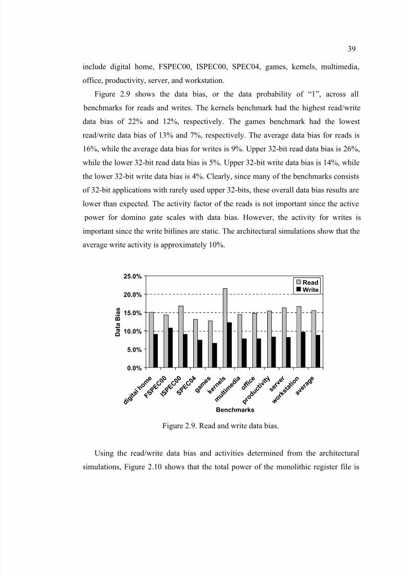
8/6/2019 Advanced Micro Architecture and Circuit Design Techniques for on-Chip Memories in CMOS Technology
http://slidepdf.com/reader/full/advanced-micro-architecture-and-circuit-design-techniques-for-on-chip-memories 55/131
39
include digital home, FSPEC00, ISPEC00, SPEC04, games, kernels, multimedia,
office, productivity, server, and workstation.
Figure 2.9 shows the data bias, or the data probability of “1”, across all
benchmarks for reads and writes. The kernels benchmark had the highest read/write
data bias of 22% and 12%, respectively. The games benchmark had the lowest
read/write data bias of 13% and 7%, respectively. The average data bias for reads is
16%, while the average data bias for writes is 9%. Upper 32-bit read data bias is 26%,
while the lower 32-bit read data bias is 5%. Upper 32-bit write data bias is 14%, while
the lower 32-bit write data bias is 4%. Clearly, since many of the benchmarks consists
of 32-bit applications with rarely used upper 32-bits, these overall data bias results are
lower than expected. The activity factor of the reads is not important since the active
power for domino gate scales with data bias. However, the activity for writes is
important since the write bitlines are static. The architectural simulations show that the
average write activity is approximately 10%.
0.0%
5.0%
10.0%
15.0%
20.0%
25.0%
d i g i
t a l h
o m e
F S P E
C 0 0
I S P E
C 0 0
S P E C
0 4
g a m e
s
k e r n e l s
m u l t i m
e d i a
o f f i c
e
p
r o d u c t i v i t y
s e r v e r
w
o r k s
t a t i o n
a v e r a g e
Benchmarks
D a
t a B i a s
ReadWrite
Figure 2.9. Read and write data bias.
Using the read/write data bias and activities determined from the architectural
simulations, Figure 2.10 shows that the total power of the monolithic register file is

8/6/2019 Advanced Micro Architecture and Circuit Design Techniques for on-Chip Memories in CMOS Technology
http://slidepdf.com/reader/full/advanced-micro-architecture-and-circuit-design-techniques-for-on-chip-memories 56/131
40
the largest compared to multi-banked and multi-frequency register files. The total
power of the register file incorporates decoder leakage, decoder active, array leakage,
and array active. The effectiveness of each technique improves as the number of ports
increase, showing a good scaling trend for wide-issue microprocessors. The multi-
banking technique improves the total register file power by 16%-32%, compared to a
monolithic register file for 4-wide to 8-wide machines. The multi-frequency technique
improves the total power by 27%-30%, compared to a monolithic register file for 4-
wide to 8-wide machines. By using multi-banking and multi-frequency in
combination, the total power improves by 34%-48%, compared to a monolithic
register file for 4-wide to 8-wide machines. These results show that multi-banking and
multi-frequency are effective techniques for reducing total power consumption, but are
even more so when used in combination.
0.00
0.50
1.00
1.50
2.00
2.50
3.00
3.50
4.00
4.50
4 G H z
, 8 R /
4 W
4 G H z
, 2 x 4 R /
4 W
8 G H z
, 4 R /
2 W
8 G H z
, 2 x 2 R
/ 2 W
4 G H z
, 1 2 R /
6 W
4 G H z
, 2 x 6 R /
6 W
8 G H z
, 6 R /
3 W
8 G H z
, 2 x 3 R
/ 3 W
4 G H z
, 1 6 R
/ 8 W
4 G H z
, 2 x 8 R /
8 W
8 G H z
, 8 R /
4 W
Register File Configuration
T o t a l P o w e r
Decoder Leakage
Decoder Active
Array Leakage
Array Active
Figure 2.10. Decoder and array power distribution.
Figure 2.11 shows that reducing the read/write data bias and activities will
decrease the active power of the register file, allowing the leakage power to become a
more dominant percentage of the overall power. For the 8R/4W register file
configuration, the monolithic register file consumes the largest percentage of leakage

8/6/2019 Advanced Micro Architecture and Circuit Design Techniques for on-Chip Memories in CMOS Technology
http://slidepdf.com/reader/full/advanced-micro-architecture-and-circuit-design-techniques-for-on-chip-memories 57/131
41
power at 28%, while the multi-banked register file consumes slightly less leakage at
27%. Multi-frequency with and without multi-banking reduces the percentage of
leakage power to 19% for the 8R/4W case. The differences in leakage percentage
become more evident for the wider issue machines, showing that multi-banking and
multi-frequency in combination reduces the leakage percentage the most. A
monolithic 16R/8W register file has 32% leakage component, while multi-banking
reduces this to a 29% component. A multi-frequency based 16R/8W register file has
19% leakage power; however, in combination with multi-banking the leakage
percentage reduces to 18%. Based on these results, multi-banking and multi-frequency
used separately or together, show good scaling trend to reduce leakage power for wide
execution machines.
0%10%20%30%40%50%60%70%80%90%
100%
4 G H z
, 8 R /
4 W
4 G H z
, 2 x 4 R /
4 W
8 G H z
, 4 R /
2 W
8 G H z
, 2 x 2 R
/ 2 W
4 G H z
, 1 2 R /
6 W
4 G H z
, 2 x 6 R /
6 W
8 G H z
, 6 R /
3 W
8 G H z
, 2 x 3 R
/ 3 W
4 G H z
, 1 6 R
/ 8 W
4 G H z
, 2 x 8 R /
8 W
8 G H z
, 8 R /
4 W
8 G H z
, 2 x 4 R
/ 4 W
Register File Configuration
P
o w e r D i s t r i b u t i o n Active
Leakage
Figure 2.11. Active and leakage power distribution.
The power density in microprocessor designs, particularly in the integer register
file, have dramatically increased due to high frequencies and process scaling. Power
density is important since it increases the junction temperature and forces power
delivery requirements to become more stringent. Power density is calculated by
dividing the worst-case total power by the register file layout area. Power density will

8/6/2019 Advanced Micro Architecture and Circuit Design Techniques for on-Chip Memories in CMOS Technology
http://slidepdf.com/reader/full/advanced-micro-architecture-and-circuit-design-techniques-for-on-chip-memories 58/131
42
increase if the total worst-case power increases and/or the area decreases. If power
density is a concern, multi-banking improves the power density compared to a
monolithic design by 22%-31% for 4-wide to 8-wide machines. Multi-frequency based
register files increase the power density by 102%-126% compared to the monolithic
esign, because the reduction in area is much larger than the decrease in total worst-
case power. Adding multi-banking to the multi-frequency designs, the power density
improves by approximately 2x; however the power density is still higher compared to
the monolithic case. Register files that use multi-banking and multi-frequency in
combination increase power density by 51%-68% for 4-wide to 8-wide machines. By
increasing the layout area of the multi-frequency designs, power density can be traded-
off to meet the design requirements.
0.00
0.50
1.00
1.50
2.00
2.50
3.00
3.50
4 G H z
, 8 R /
4 W
4 G H z
, 2 x 4 R /
4 W
8 G H z
, 4 R /
2 W
8 G H z
, 2 x 2 R
/ 2 W
4 G H z
, 1 2 R /
6 W
4 G H z
, 2 x 6 R /
6 W
8 G H z
, 6 R /
3 W
8 G H z
, 2 x 3 R
/ 3 W
4 G H z
, 1 6 R
/ 8 W
4 G H z
, 2 x 8 R /
8 W
8 G H z
, 8 R /
4 W
8 G H z
, 2 x 4 R
/ 4 W
Register File Configuration
P o w e r D e n i s t y
Figure 2.12. Power density comparison.

8/6/2019 Advanced Micro Architecture and Circuit Design Techniques for on-Chip Memories in CMOS Technology
http://slidepdf.com/reader/full/advanced-micro-architecture-and-circuit-design-techniques-for-on-chip-memories 59/131
43
Table 2.2.(a)128-entry (b) 256-entry Summary of Comparisons.

8/6/2019 Advanced Micro Architecture and Circuit Design Techniques for on-Chip Memories in CMOS Technology
http://slidepdf.com/reader/full/advanced-micro-architecture-and-circuit-design-techniques-for-on-chip-memories 60/131
44
2.5.Active Power Reduction using Multi-Bit Widths
Current modern microprocessors typically use 64-bit datapath; however, many of
the applications still use 32-bit instructions extensively [2.20]-[2.22]. We refer to these
instructions as having an architectural data size of 32-bits since they are architecturally
limited to operating on 32-bit values. In addition, there are many applications that use
64-bit instructions but the effective data size for an operand may be less than 32-bits.
This section considers the use of a multi-bit width register file to enable register reads
and writes of the fewer bits when the effective data size of a data item is smaller than
64-bits.
0%
10%
20%
30%
40%
50%
60%
70%
80%
90%
100%
d i g i t a l h
o m e
F S P E
C 0 0 I S P E
C 0 0 S P E C 0 4 g a
m e s k e
r n e l s
m u l t i m
e d i a o f f i c e
p r o d u c t i v i t y s e r v e r
w o r k s t a
t i o n a v e r a g e
Benchmarks
R e a
d O p e r a
t i o n
D i s t r i b u
t i o n
8-bit
16-bit
32-bit
64-bit
Figure 2.13. 8-bit/16-bit/32-bit/64-bit read instruction distribution.
Multi-bit width operations show similar usage of narrow bit-widths between
reads/writes. Figure 2.13 shows the distribution of the 8-bit to 64-bit read operations
across benchmarks. On average, 18% of the operations are 64-bit, while 75% are 32-
bit. 8-bit/16-bit operations are 5% and 2% of the operations, respectively. The
benchmark office has the lowest percentage of 64-bit operations at 3%, while the
benchmark FSPEC00 has the highest percentage of 64-bit operations at 53%. Figure
2.14 shows the distribution of the write operations across benchmarks. On average,

8/6/2019 Advanced Micro Architecture and Circuit Design Techniques for on-Chip Memories in CMOS Technology
http://slidepdf.com/reader/full/advanced-micro-architecture-and-circuit-design-techniques-for-on-chip-memories 61/131
45
21% of the operations are 64-bit, while 72% are 32-bit. 8-bit/16-bit operations are 5%
and 2% of the operations, respectively. The benchmark office has the lowest
percentage of 64-bit operations at 4%, while the benchmark FSPEC00 has the highest
percentage of 64-bit operations at 55%.
0%
10%
20%
30%
40%
50%
60%
70%
80%
90%
100%
d i g i t a l h
o m e
F S P E
C 0 0
I S P E
C 0 0
S P E C
0 4
g a m e
s
k e r n e l s
m u l t i m
e d i a
o f f i c
e
p r o d u c t i v i t y
s e r v e r
w o r k s t a
t i o n
a v e r a g e
Benchmarks
W r i t e O p e
r a t i o n D i s t r i b u t i o n
8-bit
16-bit
32-bit
64-bit
Figure 2.14. 8-bit/16-bit/32-bit/64-bit write instruction distribution.
Since on average, 82% of the read operations and 79% of the write operations are
32-bits or less, it is possible to reduce the register file read/write power for these
operations. Figure 2.15 shows an example of a monolithic 8R/4W 128x64b register
file organization that gates the upper and lower 32-bits separately. By placing the
decoder in the middle of the array, the upper and lower 32-bit partitions can be read
separately. For example, when a 32-bit read occurs, the upper order bits are not
necessary. The en64 signal gates the upper order clock drivers and wordlines, reducing
the active read power. Likewise, this signal gates the upper order clock drivers and
wordlines for the writes too.

8/6/2019 Advanced Micro Architecture and Circuit Design Techniques for on-Chip Memories in CMOS Technology
http://slidepdf.com/reader/full/advanced-micro-architecture-and-circuit-design-techniques-for-on-chip-memories 62/131
46
Figure 2.15. Multi-bit width register file example.
Figure 2.16 and 2.17 shows the percentage of active read/write power saved across
benchmarks. On average across all benchmarks, a multi-bit width register file saves
12% and 11% of active read/write power, respectively. A multi-bit width register file
is most effective for reducing active read power for multi-frequency designs, and is
least effective for multi-banked designs. A multi-bit width register file is most
effective for reducing active write power for multi-banked designs, and is least
effective for multi-frequency designs. The multi-bit width technique is least effective
for the FSPEC00 benchmark, where there are a high percentage of 64-bit read/write
operations. However, a multi-bit width register file still saves 7% and 6% of active
read/write power in this benchmark, respectively. In the office benchmark, where the
percentage of 32-bit operations is the highest, a multi-bit width register file saves from
15% and 13% active read/write power, respectively.
2.6. Conclusion
Using technology and architectural parameters, this chapter describes an area,
frequency, and power model for multi-ported register files. Unlike previously reported
models, REGMOD incorporates leakage power, which is becoming a dominant portion of overall power in modern register files. Comparisons of integer register files
for 4-wide to 8-wide issue machines in 65nm CMOS show that using both multi-
banking and multi-frequency techniques together reduce area by 56%-67%, total
average power by 34%-48%, leakage power by 57%-71%, and active power by 25%-
36%. Across a wide range of benchmarks, up to 12% active read power and 11%
8/6/2019 Advanced Micro Architecture and Circuit Design Techniques for on-Chip Memories in CMOS Technology
http://slidepdf.com/reader/full/advanced-micro-architecture-and-circuit-design-techniques-for-on-chip-memories 63/131
47
active write power reduction is achieved using active 32b/64b multi-bit width register
files. Multi-banking, multi-frequency, and multi-bit width register file designs show
good promise in reducing area, improving frequency, and lowering active and leakage
power for future multi-ported register files in wide-issue machines.
0.0%
2.0%
4.0%
6.0%
8.0%
10.0%
12.0%
14.0%
16.0%
d i g i t a l h
o m e
F S P E
C 0 0
I S P E
C 0 0
S P E C
0 4 g a m e
k e r n e l s
m u l t i m
e d i a
o f f i c
e
p r o d
u c t i v i t y
s e r v e r
w o r k s t a
t i o n
a v e r a g e
Benchmarks
% A c t i v
e R e a d P o w e r S a v e d
4GHz, 8R/4W
4GHz, 2x 4R/4W
8GHz, 4R/2W
8GHz, 2x 2R/2W
Figure 2.16. Average read power savings.
0.0%
2.0%
4.0%
6.0%
8.0%
10.0%
12.0%
14.0%
d i g i t
a l h o
m e
F S P E
C 0 0
I S P E
C 0 0
S P E C
0 4 g a m e
k e r n e l s
m u l t i m
e d i a
o f f i c
e
p r o d u c t i v i t y
s e r v e r
w o r k s t a
t i o n
a v e r a g e
Benchmarks
% A c
t i v e
W r i t e
P o w e r
S a v e
d
4GHz, 8R/4W
4GHz, 2x 4R/4W
8GHz, 4R/2W
8GHz, 2x 2R/2W
Figure 2.17. Average write power savings.

8/6/2019 Advanced Micro Architecture and Circuit Design Techniques for on-Chip Memories in CMOS Technology
http://slidepdf.com/reader/full/advanced-micro-architecture-and-circuit-design-techniques-for-on-chip-memories 64/131
48
References
[2.1] P. Shivakumar and N. Jouppi, “CACTI 3.0: an integrated cache timing, power,
and area Model,” WRL Research Report 2001/2, Compaq Computer
Corporation, Western Research Laboratory, Aug. 2001.
[2.2] K. Buyuksahin, et al., “ESTIMA: An architectural-level power estimator for
multi-ported pipelined register files,” in Proceedings International Symposium
Low Power Electronics Design, Aug. 2003, pp. 294-297.
[2.3] V. Zyuban, et al., “The energy complexity of register files,” in Proceedings International Symposium Low Power Electronics Design, Aug. 1998, pp. 305-310.
[2.4] K. Ghose, et al., “Reducing power in superscalar processor caches using
subbanking, multiple line buffers and bitline segmentation,” in Proceedings International Symposium Low Power Electronics Design, Aug. 1999, pp. 70-
75.
[2.5] X. Zhao, et al., “Structure Configuration of Low Power Register File Using
Energy Model,” in Proceedings Asia-Pacific Conference ASIC , Aug. 2002, pp.
41-44.
[2.6] J. Butts and G. Sohi, “A static power model for architects,” in Proceedings33
rd International Symposium Microarchitecture, Dec. 2000, pp. 191-201.
[2.7] S. Heo and K. Asanovic, “Leakage-biased domino circuits for fine-grainleakage reduction,” in Symposium VLSI Circuits Digest Technical Papers, June
2002, pp. 316-319.
[2.8] S. Rusu, et al., “A dual-core multi-threaded Xeon® processor with 16MB L3
cache,” in International Solid-State Circuits Conference Digest Technical
Papers, Feb. 2006, pp. 102-103.
[2.9] D. Sima, et al., “The design space of register renaming techniques,” IEEE
Micro, vol. 20, pp. 70-83, Sept. 2000.
[2.10] R. Kessler, “The Alpha 21264 microprocessor,” IEEE Micro, vol. 19, pp. 24-36, April 1999.
[2.11] R. Preston, et al., “Design of an 8-wide superscalar RISC microprocessor with
simultaneous multithreading,” in International Solid-State Circuits Conference
Digest Technical Papers, Feb. 2002, pp. 334-335.

8/6/2019 Advanced Micro Architecture and Circuit Design Techniques for on-Chip Memories in CMOS Technology
http://slidepdf.com/reader/full/advanced-micro-architecture-and-circuit-design-techniques-for-on-chip-memories 65/131
49
[2.12] I. Nishi, et al., “A 1GIPS 1W single-chip tightly-coupled four-way
multiprocessor with architecture support for multiple control flow execution,”
in International Solid-State Circuits Conference Digest Technical Papers, Feb.2000, pp. 418-419.
[2.13] J. Tseng, et al., “Banked multiported register files for high-frequencysuperscalar microprocessors,” in Proceedings 30
thInternational Symposium
Computer Architecture, June 2003, pp. 62 -71.
[2.14] J. Cruz, et al., “Multi-banked register file architectures,” in Proceedings 27 th
International Symposium Computer Architecture, June 2000, pp. 316-325.
[2.15] N. Kim, et al., “The microarchitecture of a low power register file,” in Proceedings International Symposium Low Power Electronics Design, Aug.
2003, pp. 384-389.
[2.16] S. Wijeratne, et al., “A 9GHz 65nm Intel Pentium® 4 Processor Integer
Execution Core,” in International Solid-State Circuits Conference Digest Technical Papers, Feb. 2006, pp. 110-111.
[2.17] K. Endo, et al., “Pipelined, time-sharing access technique for an integrated
multiported memory,” IEEE Journal Solid State Circuits, vol. 26, pp. 549-554,
April 1991.
[2.18] T. Takayanagi, et al., “350MHz time-multiplexed 8-port SRAM and word-size
variable multiplier for multimedia DSP,” in International Solid-State Circuits
Conference Digest Technical Papers, Feb. 1996, pp. 150-151.
[2.19] P. Bai, et al., “A 65nm logic technology featuring 35nm gate lengths, enhance
channel strain, 8 Cu interconnect layers, low-k ILD and 0.57µm2
SRAM cell,”
in International Electron Devices Meeting Technical Digest , Dec. 2004, pp.657-660.
[2.20] M. Kondo, et al., “A small, fast and low-power register file by bit- partitioning,” in Proceedings 11
thInternational Symposium High-Performance
Computer Architecture, Feb. 2005, pp. 40-49.
[2.21] D. Brooks and M. Martonosi, “Value-based clock gating and operation packing: dynamic strategies for improving processor power and performance,” ACM Transactions on Computer Systems, vol. 18, pp. 89-126, May 2000.
[2.22] S. Balakrishnan and G.H. Sohi, “Exploiting value locality in physical register
files,” in Proceedings 36 rd
International Symposium Microarchitecture, Dec.
2003, pp. 265-276.
8/6/2019 Advanced Micro Architecture and Circuit Design Techniques for on-Chip Memories in CMOS Technology
http://slidepdf.com/reader/full/advanced-micro-architecture-and-circuit-design-techniques-for-on-chip-memories 66/131
50
DYNAMIC ADDRESSING MEMORY ARRAYS
WITH PHYSICAL LOCALITY
Steven K. Hsu, Shih-Lien Lu, Shih-Chang Lai, Ram K. Krishnamurthy, Konrad Lai
36th
International Symposium on Microarchitecture
IEEE MICRO-36, 2004

8/6/2019 Advanced Micro Architecture and Circuit Design Techniques for on-Chip Memories in CMOS Technology
http://slidepdf.com/reader/full/advanced-micro-architecture-and-circuit-design-techniques-for-on-chip-memories 67/131
51
3. MULTI-LATENCY ACCESS REGISTER FILES
3.1. Introduction
One of the important memory arrays in a superscalar processor is the register file
since it communicates results between computations. Renaming architecture registers
to physical registers allows the removal of anti-dependencies. The physical register
file is usually much larger than the architecture register file to exploit parallelism.
Moreover, since multiple instructions are issued in a cycle, physical register files are
multi-ported contributing to the rapid size growth of register files. In order to shorten
the access time, register files designs use single-ended full-swing domino circuits
instead of the differential small swing design used in a large cache structure. These
factors all contribute to the size growth of the register file and thus increase the access
time. To understand the size, a typical 256-entries 64-bit 8-read / 4-write register file
will need more than half a million transistors to implement the array itself excluding
the address decoding, peripheral, and control circuits.
The sheer size of the register file will affect the access time. Currently, a single
cycle register file latency access will no longer be feasible because of the amount of
interconnect the signal needs to travel from address generation to the output of the
memory array. As cycle times become less, the amount of interconnect distance a
signal can travel in a single cycle will be less forcing designs to allocate multiple
cycles for a single access to the register file affecting the performance of the
microprocessor [3.7].
Two-level register file architectures have been proposed [3.8][3.9] to mitigate the
latency problem of multi-cycle register files. This type of design employs a smaller
but faster memory structure containing a part of all information from the originalregister file. Most of the access will be to the register file cache, which is faster. It
improves the average access latency to the register file by exploiting locality.
Inclusion is maintained, that is, data in the cache should be found in the register file.
With inclusion, tag checking must be performed to find out if the data is in the cache
or not. This introduces complexity in scheduling of dependent instructions because the

8/6/2019 Advanced Micro Architecture and Circuit Design Techniques for on-Chip Memories in CMOS Technology
http://slidepdf.com/reader/full/advanced-micro-architecture-and-circuit-design-techniques-for-on-chip-memories 68/131
52
presence of accessed data in the cache determines the total latency of the instruction.
Also, this scheme only introduces another level of hierarchy in the memory pyramid.
Thus it is advantageous to have a register file design that has shorter average latency
but has known access time before an instruction is scheduled. Circuit and
microarchitecture techniques to the traditional register file design exploits physical
locality and has a known access time at the time of scheduling. Part of the register file
is faster than the other part because it is closer to the peripheral circuit. The access
time depends solely on the location of the register’s physical location and thus can be
pre-determined prior to the scheduling of instructions.
If the access time to the queue depends on the physical location, then it is desirable
to increase the occurrence of accesses to the fast array. This chapter further proposes a
simple address decoding modification, allowing address-mapping reconfiguration to
increase the frequency of usage in the fast array of the register file. This method
checks the physical register file, which is organized as a circular queue at the decode
time. Whenever a slower entry is allocated for storing the destination, it checks the
pointers used to keep track of the circular queue. If the faster counter part of the queue
is un-used, a bit is set to indicate that the data can be duplicated into that entry. Upon
completing the execution of the instruction, the result is stored in both the original place and the duplicated place if the bit is set. Subsequent read from the register file’s
address logic is designed so that it will read from the faster part of the array. This
method only requires a small 1-bit wide table to indicate an entry has a valid
duplicated copy or not. Some minor modification to the address decoding logic is also
needed.
3.2. Register File Architecture
3.2.1. Conventional Register File
Current high-performance processors all utilize register renaming to remove anti-
dependency. One implementation scheme utilizes three array structures besides the
architecture register file. The array structures include: the rename table, the physical
register file (RF) and the re-order buffer (ROB). The rename table contains the

8/6/2019 Advanced Micro Architecture and Circuit Design Techniques for on-Chip Memories in CMOS Technology
http://slidepdf.com/reader/full/advanced-micro-architecture-and-circuit-design-techniques-for-on-chip-memories 69/131

8/6/2019 Advanced Micro Architecture and Circuit Design Techniques for on-Chip Memories in CMOS Technology
http://slidepdf.com/reader/full/advanced-micro-architecture-and-circuit-design-techniques-for-on-chip-memories 70/131
54
entries that are closer to the peripheral circuit and can be accessed faster than entries
that are physically further away.
3.2.2. Variable Cycle Register File
In order to achieve fast access time with multiple ports, register file’s data lines
(called bitlines) are designed with singled-ended full swing dynamic circuits. Each
storage cell, a cross-coupled inverter, drives a pull-down n-type device, which is
connected in series to the dynamic node (bitline). With leakage current increasing, the
number of rows (entries) that are on bitline segment is limited in order to read out data
reliably. For the sub-100nm generation technology, this number is less than ten. This
bitline is referred to as the local bitline (LBL). Typically two local bitlines are mergedusing a static NAND gate and the output of the NAND gate is fed into another
dynamic NOR gate with other merged local bitlines. Depending on the number of
register entries in the register file there may be several levels of these dynamic-static
(domino) stages arranged as a tree structure implementing a wide OR operation. For
example, a 256-entries register file is arranged with 8 entries per local bitline. Two
local bits are merged with a static NAND gate. Eight of these merged local bitlines
(total of 16 local bitlines) are combined on a global bitline. Thus, each global bitline
has 128 entries. Finally, two global bitlines are merged with a static NAND to
complete 256 entries.
This tree structure is usually perfectly balanced to allow a uniform access time
independent of which entry is read. In our previous example, the final merged NAND
is usually placed in the middle of the two global bit lines and a final wire segment
covering the length of half the entries must be used to bring the final output out of the
array. It is not essential to make the tree well balanced having the same access time as
long as the scheduler knows about it ahead of time. Thus, the organization can be
arranged to allow the entries physically closer to the peripheral circuit that drive the
output to be read out and be latched first. The other half can be read out through the
original wire used to read out the merged output. In this way the access to the first half
is faster than the original speed while the access to the second remains the same. This

8/6/2019 Advanced Micro Architecture and Circuit Design Techniques for on-Chip Memories in CMOS Technology
http://slidepdf.com/reader/full/advanced-micro-architecture-and-circuit-design-techniques-for-on-chip-memories 71/131
55
chapter will discuss the detail arrangement and quantify the speed difference using a
next generation technology in section 3. The proposed technique observes that the
register file may be designed to enable the access of the front half of the entries to be
faster than access over the end half due to physical locality.
However, the locations of the fast access are fixed since this is dependent of the
physical layout of the actual transistors. In the example, at least half of the time the
access time is the same as before. Maximizing performance can be achieved by
increasing the probability that an access will hit the faster part of the register file. A
simple method is proposed.
3.2.3. Increasing the Use of Fast Registers
To summarize, the method duplicates the new data into the unused space whenever
possible. When the space storing the duplicated data is needed; it is simply written
over. A small 1-bit table with n/2 entries is maintained to indicate an entry with slower
access time has a valid duplicated copy, where n is the number of entries in the
register file. This table is called the swap register table. Any access to an slow entry
with valid duplicated copy is automatically decoded to load from the duplicated site
that has shorter access latency. Whenever the corresponding bit is set, there is a valid
duplicated entry.
The proposed method can be explained by using a simple circular queue with four
entries as an example. Half of the entries (the shaded top two entries) have a shorter
access time. The other half (un-shaded bottom two entries) has longer access time. The
data items are numbered to be loaded into the queue from 0 on. Figure 3.1 details an
example sequence of operations. This circular queue is maintained with two pointers
HEAD (H) and TAIL (T). Initially both the HEAD (H) and TAIL (T) pointers are
pointing to the first location of the array. At this time, the queue is now empty. The
first set of operations consist of allocating three entries (0, 1, 2) for writes. The TAIL
pointer is move to point to the fourth entry while the HEAD pointer remains at the
beginning as shown. If there are random read accesses to the queue at this time, then
two thirds of the accesses will hit the portion of the queue with shorter access time.

8/6/2019 Advanced Micro Architecture and Circuit Design Techniques for on-Chip Memories in CMOS Technology
http://slidepdf.com/reader/full/advanced-micro-architecture-and-circuit-design-techniques-for-on-chip-memories 72/131
56
The second set of operations consists of releasing two items from the queue.
Afterward, the HEAD pointer is pointing to entry 3 and the TAIL pointer remains at
the same location. Accesses to the queue at this time will have a longer access time.
Later, a new allocation for write occurs. Since the “corresponding” entry in the faster
half is un-occupied, a duplicated copy is written. A fast entry can be determined to be
un-occupied by comparing the value of the HEAD pointer and the entry address. If
duplication is allowed, data is written into both places. This is achieved through a
modification to the decoding logic to allow two word lines to be enabled during the
write operation. A bit will be set to indicate that a valid duplicated version is available.
After this bit has been set, accesses to the queue will land on the faster part half the
time through a modified decoding logic. If it had not been duplicated, then all access
will hit the slower part instead. This example continues with two more allocations
(entries 0, 1) for writing data 4 and 5. Then the queue is full and half of the accesses
will have shorter cycle time. Notice that the first new allocation basically writes over
the duplicated item. The bit used to indicate the duplicated data in the faster section is
cleared when the entry is over written. A few more operations continue in the example
as shown.
ALLOCATE 0, 1, 2012
T H
T
H
2T
H
RELEASE 0, 1
(3)
23
T
HALLOCATE 3 5
TH
RELEASE 2, 3, 4
(6)56
T
HALLOCATE 6 (6)
6T
H
RELEASE 5 (6)(7)6
7
T
H
ALLOCATE 7
(7)
7
T
H
RELEASE 6
4523
T H
ALLOCATE 4, 5
full
Start:empty
8(7)
7
T
H
ALLOCATE 88
THRELEASE 7
00
00
00
Swap
register
table
10
00
00
01
01
1
1
10
00
10
Note: (n) mean the item “n” is duplicated
Figure 3.1. Re-configurable addressing example.

8/6/2019 Advanced Micro Architecture and Circuit Design Techniques for on-Chip Memories in CMOS Technology
http://slidepdf.com/reader/full/advanced-micro-architecture-and-circuit-design-techniques-for-on-chip-memories 73/131

8/6/2019 Advanced Micro Architecture and Circuit Design Techniques for on-Chip Memories in CMOS Technology
http://slidepdf.com/reader/full/advanced-micro-architecture-and-circuit-design-techniques-for-on-chip-memories 74/131
58
ports. Since each port will need a bitline, there will be total of 12 bitlines and 12 word
lines.
Entry 0
Decoder(Cycle 1)
Array(Cycle 2)
Entry 127
Entry 128
Entry 255
Data Output [63:0]
Data Input [63:0]
8 Read Address[7:0]
Array(Cycle 2)
Global Merge(Cycle 3)
1 0 0 0 μ m
4 Write Address[7:0]
125μm370μm 370μm
338μm 338μm
338μm 338μm
Figure 3.2. Example conventional register file design.
Figure 3.2 shows an example design of a conventional register file for a 256x64b
8R/4W register file with physical dimension depicted. The register file decoder and
array occupies a dense layout of 865µm x 100µm. This dimension is obtained from
actual layout using an advanced CMOS 90nm process. This register file is pipelined
and requires three-cycles for a read access. As shown, the array is split into half with
the decoder in the middle to reduce word line length and achieve higher performance.
The first cycle is attributed to the decoding of the address. Typically, the decoder is
non-critical and can easily meet timing. The second cycle is attributed to the word line
activation, local bit line discharge and a section of the global bit line discharge. The
global bit line is partitioned in to separate bit lines with domino repeaters due to the

8/6/2019 Advanced Micro Architecture and Circuit Design Techniques for on-Chip Memories in CMOS Technology
http://slidepdf.com/reader/full/advanced-micro-architecture-and-circuit-design-techniques-for-on-chip-memories 75/131
59
excessive resistive interconnect length. The third cycle is attributed to the final global
bit line merge between arrays. The final global merge forces the design to a 3-cycle
register file, since delay is heavily dominated by interconnect. The data is delivered at
the bottom of the middle array for a balanced access time for the receiving functional
unit.
Decoders are implemented as wide AND gates. A 256-entry register file needs 8
address inputs to determine which entry is selected. There needs to be a decoder for
each write and read ports. Dynamic or static CMOS logic implementations are both
acceptable, static CMOS logic design gives lower power since clock nodes are not
discharged and charged every cycle and maintains a low activity factor. The design
implements a fully static decoder, since it can be done comfortably in a single clock
cycle. The decoder feeds the word line drivers and is set up well ahead of the rising
edge of the second cycle.
R e a d B i t l i n e a [ 0 ]
R e a d B i t l i n e a [ 7 ]
W r
i t e B i t l i n e a [ 0 ]
W r
i t e B i t l i n e a [ 3 ]
Write Wordline a[0]
Write Wordline a[3]
Read Wordline a[7]
Read Wordline a[0]
M2
M3
Figure 3.3. 8-read 4-write register file cell.
Figure 3.3 shows an example 8 read 4 write register file cell. Heavily multi-ported
arrays are interconnect dominated by minimum pitch metal 3 (M3) tracks for word

8/6/2019 Advanced Micro Architecture and Circuit Design Techniques for on-Chip Memories in CMOS Technology
http://slidepdf.com/reader/full/advanced-micro-architecture-and-circuit-design-techniques-for-on-chip-memories 76/131
60
lines and minimum pitch metal 2 (M2) or metal 4 (M4) tracks for bit lines. Typically,
the cell area is dictated in the x-dimension by M3 interconnects. The width (x
direction) is the M3 pitch multiplied by the # of read + write ports. The M2 and M4
wires dictate the y-dimension. Thus the height (y direction) equals to M4 wire pitch
multiplied by the # of read + write ports + power. As the number of ports increases,
the cell area will increase also since it is interconnect limited.
Read Wordline a[0]
Read Wordline g[0]
Clock
L o c a l B i t l i n e a [ 0 ]
Local Bitline a[1]
GBL
M2
M3
Figure 3.4. Bitline structure.
Local bitlines are implemented in single rail 2-phase domino logic. Domino logic
is the most efficient way to implement large fan-in logic gates and will give the
highest performance. The bitlines are limited by leakage and interconnect length. The
leakage of the read ports on the local bitline injects noise on the dynamic node during
evaluation. The dynamic node is only weakly held by a keeper to prevent the leakage
from causing a false evaluation. The resistance of the interconnect sets the maximum
length allowed for a global bitline evaluation in a single phase. The local bitline is
routed on minimum pitch M2, and the global bitline (GBL) is routed on a higher-level
metal minimum pitch M4. In this example design the half-shielded local bitline is
61um in length, while global level bitlines are 460µm long. A static 2-input NAND

8/6/2019 Advanced Micro Architecture and Circuit Design Techniques for on-Chip Memories in CMOS Technology
http://slidepdf.com/reader/full/advanced-micro-architecture-and-circuit-design-techniques-for-on-chip-memories 77/131
61
gate merges each dynamic local bitline. The NAND gate feeds into a dynamic global
bitline which is again is a wide domino OR gate. Figure 3.4 illustrates the bitline
circuits.
3.3.2. Register File with Physical Locality
A register file can be implemented to exploit physical locality. Using a simple
rearrangement of the final global merge of the register file, the array can now deliver
an entry in two or three cycles, depending on the physical location of the entry. Worst
case read accesses in this new register file are the same as the worst case read access
for conventional register files. Therefore worst-case performance can be no worst than
conventional performance. However, best case read access latency would be 1 cyclefaster than the conventional case.
Entry 0
Decoder
(Cycle 1)
Fast
Array
(Cycle 2)
Entry 127
Entry 128
Entry 255
Data Output [63:0]
Slow
Array(Cycle 2)
Global Merge(Cycle 3)
Data Input [63:0]
8 Read Address[7:0]4 Write Address[7:0]
1 0 0 0 μ m
125μm370μm 370μm
676μm
338μm 338μm
Figure 3.5. Register file with physical locality.
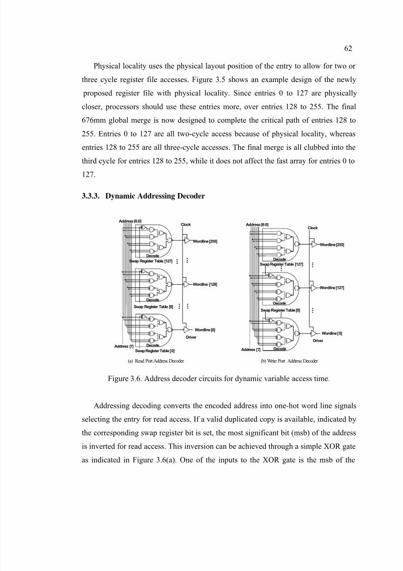
8/6/2019 Advanced Micro Architecture and Circuit Design Techniques for on-Chip Memories in CMOS Technology
http://slidepdf.com/reader/full/advanced-micro-architecture-and-circuit-design-techniques-for-on-chip-memories 78/131
62
Physical locality uses the physical layout position of the entry to allow for two or
three cycle register file accesses. Figure 3.5 shows an example design of the newly
proposed register file with physical locality. Since entries 0 to 127 are physically
closer, processors should use these entries more, over entries 128 to 255. The final
676mm global merge is now designed to complete the critical path of entries 128 to
255. Entries 0 to 127 are all two-cycle access because of physical locality, whereas
entries 128 to 255 are all three-cycle accesses. The final merge is all clubbed into the
third cycle for entries 128 to 255, while it does not affect the fast array for entries 0 to
127.
3.3.3. Dynamic Addressing Decoder
Clock
Wordline [255]
Driver
Wordline [0]
Swap Register Table [127]
Swap Register Table [0]
Decode
Address [6:0]
Wordline [128]
Swap Register Table [0]
Address [7]
Decode
Decode
Clock
Wordline [255]
Driver
Wordline [0]
Swap Register Table [127]
Decode
Address [6:0]
Wordline [127]
Swap Register Table [0]
Address [7]
Decode
Decode
(b) Write Port Address Decoder (a) Read Port Address Decoder
Figure 3.6. Address decoder circuits for dynamic variable access time.
Addressing decoding converts the encoded address into one-hot word line signals
selecting the entry for read access. If a valid duplicated copy is available, indicated by
the corresponding swap register bit is set, the most significant bit (msb) of the address
is inverted for read access. This inversion can be achieved through a simple XOR gate
as indicated in Figure 3.6(a). One of the inputs to the XOR gate is the msb of the

8/6/2019 Advanced Micro Architecture and Circuit Design Techniques for on-Chip Memories in CMOS Technology
http://slidepdf.com/reader/full/advanced-micro-architecture-and-circuit-design-techniques-for-on-chip-memories 79/131
63
address. The other input is from the swap register table. Each entry of the swap
register table drives two XOR gates – the ith and the (i+(n/2))th. In Figure 3.6, the first
entry of the swap register table (denoted as entry [0]) drives the first and the 128th, for
example. If the incoming address is 128 (100000002) and the swap register table [0] is
set then wordline[0] will be selected (high) while wordline[128] will not be selected
(low). Using this method, the processor is able to take advantage of the faster portion
of the register file as much as possible. When the data is ready to be written into a
slow entry and there is an un-occupied entry in the fast array, indicated by the bit set
in the swap register, then both word lines are enabled. This is accomplished through
XOR gates again as shown in Figure 3.6(b).
3.4.Simulation and Result Discussion
In order to study the effect of the proposed method, circuit-level simulation as well
as microarchitecture simulation are both performed. Circuit simulation provides the
detail delay information comparison between the conventional design and our
proposed design with interconnects delay included. Microarchitecture simulation
studies the impact of having variable latency on register file and data cache read.
3.4.1. Circuit Level Simulation
0 100 200 300 400 500
S l o w
F a s t
C o n v .
R e a d A c c e s s
Cycle Time (ps)
cycle2 cycle3
wl
wl
wl
lbl
lbl
lbl
gbl
gbl
gbl
gbl
gbl
gbl
fgm
fgm
s
s
s
Figure 3.7. Data read delay timing.

8/6/2019 Advanced Micro Architecture and Circuit Design Techniques for on-Chip Memories in CMOS Technology
http://slidepdf.com/reader/full/advanced-micro-architecture-and-circuit-design-techniques-for-on-chip-memories 80/131
64
A 4GHz 90nm 256 x 64b 8R/4W register file was design and simulated with
interconnect and parasitic loads. Circuit simulation was done using a speculative 90nm
process at 1.2V and 110° Celsius using all high-threshold devices. It was found that
the conventional register file design was forced to include an extra cycle in the read
array path. Upon altering the configuration, the register file with physical locality was
able to achieve a fast and slow access within the 4GHz cycle time. Figure 3.7
illustrates the delay-timing break down of the circuit simulation for the most critical
part of the read operation – the array read. For the conventional read access, the first
phase of the second cycle includes the delay of the word line (WL) activation and
local bitline (LBL) evaluation. The second phase of the second cycle includes the two-
level global bitline (GBL) merge. Lastly, the final global merge (FGM) completes in
the third cycle and merges the two arrays with a dynamic to static (S) NAND
interface. The fast access completes within a single cycle of 250ps and is not impacted
by a final global merge (FGM), but still has the dynamic to static (S) NAND interface.
The slow access, while very similar to the conventional case, uses the first phase of the
third cycle to evaluate the final global merge (FGM) and dynamic to static (S)
interface. The unlabeled white space in Figure 3.7 includes clock skew, jitter, and
margin.
3.4.2. Architecture Simulations
The architectural simulation used a modified version of the SimpleScalar toolset
[3.11] to evaluate the performance impact on varying the register-read cycle. Ten
integer SPEC 2000 benchmarks [3.12] are used to evaluate the effect. After skipping
the first 500 million instructions, statistics for 500 million committed instructions are
collected.
The base model processor is a seven-stage pipeline micro-architecture: Fetch (FE),
Decode/Rename (DE), Schedule (SC), Register read (RE), Execution (EX), Write
back (WB) and Commit (CM). The front-end of the processor has less impact on the
IPC is assumed as suggest by [3.7]. Thus, the FE and DE take only one cycle. The
schedule stage has a 2-cycles latency, while the register-read stage has a 3-cycle

8/6/2019 Advanced Micro Architecture and Circuit Design Techniques for on-Chip Memories in CMOS Technology
http://slidepdf.com/reader/full/advanced-micro-architecture-and-circuit-design-techniques-for-on-chip-memories 81/131
65
latency. Execution cycle latency depends on the type of operation as well as
computing resource. For example, our base line model uses a 6-cycle first-level data
cache. This number is suggested by [3.5] and through our circuit level estimation. All
other stages are single-cycle. Furthermore, we scheduled the instruction at data-ready
cycle to eliminate the effect of data speculation. Table 1 summarizes the detail
processor configuration.
Table 3.1. SimpleScalar Configuration.
Description Configuration
Fetch, Decode, Schedule, Commit Width 4
Fetch/Decode/Schedule/Register/
Execute/Writeback/Commit stage latency1/1/2/3/FU-latency/1/1
Architecture Register File IO port 8 reads/ 4 writes
Branch Predictor
Branch Prediction Table
16-bits Gshare
8K-entry, 8 way
ROB/LSQ size 256/128
L1 I/D cache 32KB/32KB, 4-way, 32B line size
L1 I/D cache hit latency 1/6 cycles
L2 cache 4MB
L2 / memory latency 10/100 cycles
# of pipelined integer ALU/MULT/DIV 4/1/1
Integer ALU/MULT/DIV 2/6/40
Floating-point Adder/MULT/DIV 4/8/48
Cache Read/Write port 2
This base model, has a static RF access time of three cycles (RF-S-3) and static
level-1 data cache latency of 6 (C-S-6), represents our performance (IPC) lower
bound. The IPC performance upper bound is a processor with 2-cycles register-read
stage (RF-S-2) and 5-cycle L1 D-cache latency (C-S-5). With no address decoding
reconfiguration, our example 256x64 register file circuit design allows half of the 256
entries (0 to 127) to have faster access time (2-cycles). The other half (registers 128 to
255) of the register entries adds an extra cycle to its access time. Therefore, when an

8/6/2019 Advanced Micro Architecture and Circuit Design Techniques for on-Chip Memories in CMOS Technology
http://slidepdf.com/reader/full/advanced-micro-architecture-and-circuit-design-techniques-for-on-chip-memories 82/131
66
instruction is decoded a new physical register is allocated. If this entry is among the
first half of the register file (from 0th to 127th) then dependent instructions is
scheduled to wakeup with 2-cycle RE latency. Otherwise, this instruction allocates a
physical register among in the slower portion and all dependent instructions will be
scheduled according to 3-cycle RE latency. This design is called the RF-S-2_3 model.
The implementation of the dynamic address decoding design is called the RF-D-2_3
model. Table 2 summarizes the notation used in reporting results in the following
sections.
Table 3.2. Simulation Test Cases.
Type Shorthand Description
Static 2 cycle RF-S-2 Conventional 2 cycle reads
Static 3 cycle RF-S-3 Conventional 3 cycle reads
Static 2/3 cycle RF-S-2_3 Static 2 or 3 cycle readsRegister File
Dynamic 2/3 cycle RF-D-2_3Dynamic Addressing 2 or 3
cycle reads
Static 5 cycle C-S-5 Conventional 5 cycle reads
Static 6 cycle C-S-6 Conventional 6 cycle readsData Cache
Static 5 / 6 cycle C-S-5_6 Static 5 or 6 cycle reads
0%10%
20%
30%
40%
50%
60%
70%
80%
b z i p 2
g a p
g c c
g z i p
m c f
p a r s e r
p e r l
t w o l f
v o r t e x
v p r
a v e r a g e
RF-S-2_3 RF-D-2_3
Figure 3.8. IPC recovered for register file static and dynamic 2/3 cycle reads.

8/6/2019 Advanced Micro Architecture and Circuit Design Techniques for on-Chip Memories in CMOS Technology
http://slidepdf.com/reader/full/advanced-micro-architecture-and-circuit-design-techniques-for-on-chip-memories 83/131
67
As pipeline stages are partitioned into multiple cycles to keep the clock frequency
up, IPC is degraded. For example, one extra RE cycle (2 vs. 3) and one extra level 1
data cache latency (5 vs. 6) degrades the IPC by more than 7%. It is the goal of this
approach to recover the IPC loss while marinating the high clock frequency.
Figure 3.8 shows that if only the register file circuit is modified, recovery is only
7%~37% of the IPC lost. Average recovery is less than 20%. This is understandable
because physical register file is organized as a circular queue. Faster registers are
statically located from entries 0 to 127. Our studies revealed that all committed
instructions are evenly distributed in the faster and slower location of register file.
Depending on the access pattern, the design will only be able to recover, at the most,
50% of the IPC lost. However, with the proposed dynamic allocation of registers
through duplication increases the chance of using those faster registers. The simulation
shows that (Figure 3.9), on the average, over 80% of the dynamic instructions can take
advantage of the un-occupied space and duplicate data unto the faster part of the
register file and have shorter register read latency. With dynamic address mapping of
register file, the design is able to recover more than 50% of the IPC loss due to extra
cycles. Note for both these cases (RF-S-2_3 and RF-D-2_3), data cache latency is 6,
while the upper bound used to obtain the IPC loss has a 5 cycle level 1 data cache.
0%10%
20%30%40%50%60%70%80%90%
100%
b z i p 2
g a p
g c c
g z i p
m c f
p a r s e r
p e r l
t w o l f
v o r t e x
v p r
a v e r a g e
RF Slow Array
RF Fast Array
Figure 3.9. Register file committed instruction for RF-D_2_3 distribution.
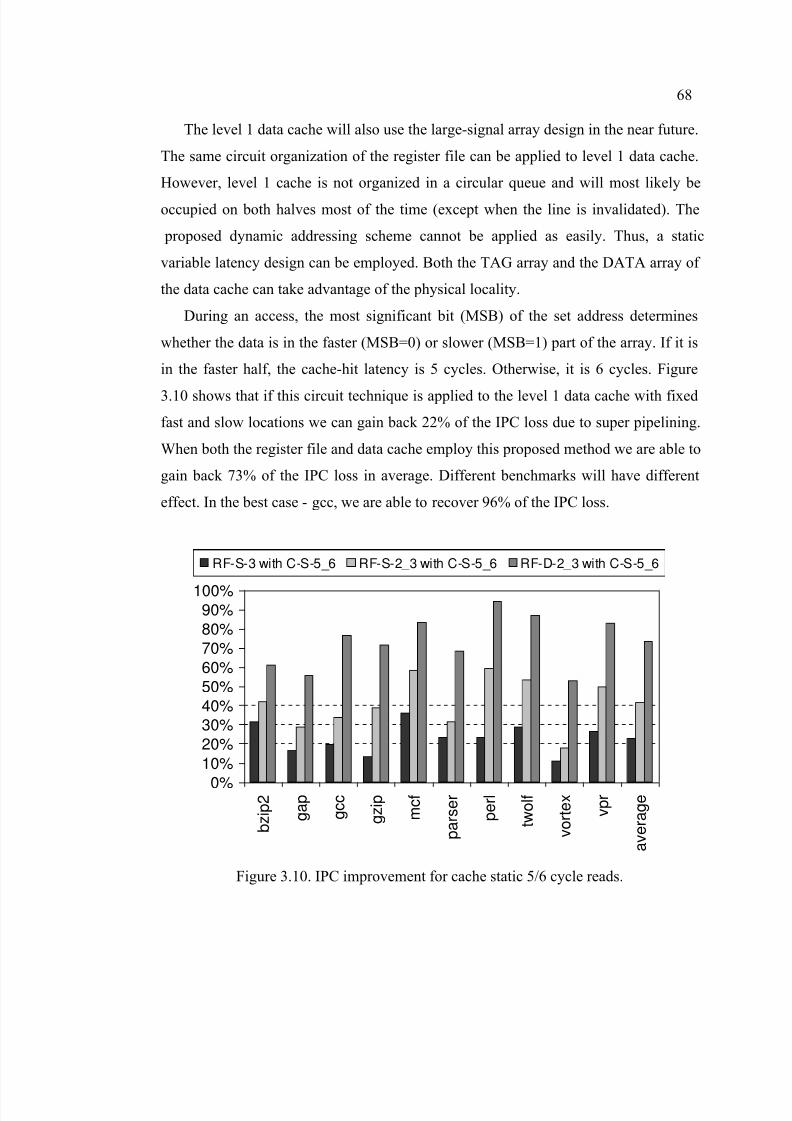
8/6/2019 Advanced Micro Architecture and Circuit Design Techniques for on-Chip Memories in CMOS Technology
http://slidepdf.com/reader/full/advanced-micro-architecture-and-circuit-design-techniques-for-on-chip-memories 84/131
68
The level 1 data cache will also use the large-signal array design in the near future.
The same circuit organization of the register file can be applied to level 1 data cache.
However, level 1 cache is not organized in a circular queue and will most likely be
occupied on both halves most of the time (except when the line is invalidated). The
proposed dynamic addressing scheme cannot be applied as easily. Thus, a static
variable latency design can be employed. Both the TAG array and the DATA array of
the data cache can take advantage of the physical locality.
During an access, the most significant bit (MSB) of the set address determines
whether the data is in the faster (MSB=0) or slower (MSB=1) part of the array. If it is
in the faster half, the cache-hit latency is 5 cycles. Otherwise, it is 6 cycles. Figure
3.10 shows that if this circuit technique is applied to the level 1 data cache with fixed
fast and slow locations we can gain back 22% of the IPC loss due to super pipelining.
When both the register file and data cache employ this proposed method we are able to
gain back 73% of the IPC loss in average. Different benchmarks will have different
effect. In the best case - gcc, we are able to recover 96% of the IPC loss.
0%
10%
20%
30%
40%
50%
60%
70%
80%
90%100%
b z i p 2
g a p
g c c
g z i p
m c f
p a r s e r
p e r l
t w o l f
v o r t e x
v p r
a v e r a g e
RF-S-3 with C-S-5_6 RF-S-2_3 with C-S-5_6 RF-D-2_3 with C-S-5_6
Figure 3.10. IPC improvement for cache static 5/6 cycle reads.

8/6/2019 Advanced Micro Architecture and Circuit Design Techniques for on-Chip Memories in CMOS Technology
http://slidepdf.com/reader/full/advanced-micro-architecture-and-circuit-design-techniques-for-on-chip-memories 85/131
69
As level 1 data cache size increases, more memory accesses will hit the cache. As
a result, it is observed that the cache-hit latency will affect the IPC degradation more.
Figure 3.11 shows that as level 1 data cache increases to 64KB, IPC loss due to longer
latency increases from 7.2% to almost 8%. However the proposed method used to
recover IPC loss is insensitive to level 1 data cache size. The percentage IPC
degradation recovered with the proposed method remains approximately the same for
three different cache sizes at 75%.
If the number of entries in a register file is small, having longer register file access
latency (thus longer pipeline) tends to apply more pressure on the physical register
file. This is because more instructions will be in-flight and a processor needs more
physical registers to accommodate them. The average physical register file occupancy
rate will be higher and there will be less chance to exploit the faster cycle time access
using the proposed re-mapping method. As the physical register file size increases,
more un-occupied spaces are available for duplication. Figure 3.12 shows that the
recovery of IPC degradation increases to 80% (the absolute performance loss is only
1.4%) as the size of the register file increases to 512 entries.
0%
1%
2%
3%
4%
5%
6%
7%
8%
9%
16KB 32KB 64KB
Cache Size
P e r f o r m a n c e L o s s
RF-S-3; C-S-6
RF-D-2_3; C-S-6
RF-D-2_3; C-S-5_6
Figure 3.11. Effect of cache size.

8/6/2019 Advanced Micro Architecture and Circuit Design Techniques for on-Chip Memories in CMOS Technology
http://slidepdf.com/reader/full/advanced-micro-architecture-and-circuit-design-techniques-for-on-chip-memories 86/131
70
0%
1%
2%
3%
4%
5%
6%
7%
8%
128 256 512
Register File Entries
P e r f o r m a n c e l o s s RF-S-3; C-S-6
RF-D-2_3; C-S-6
RF-D-2_3; C-S-5_6
Figure 3.12. Effect of register file size.
3.5. Conclusion
As issue-width increases to exploit instruction level parallelism many memory
arrays in the microprocessor must grow in size. Since wiring delay contributes greatly
to the access time of an array, multiple cycles are allocated for accessing these arrays.
This chapter proposes a circuit solution to allow the array to have variable latencydepending on the physical locality to improve the latency of loops with dependent
instructions. Furthermore, the chapter proposes a method to re-configure the address
decoding to take more advantage of this asymmetric access time for the physical
register file. To validate the new scheme, a microarchitecture simulator is used. With
dynamic addressing register file and static variable level 1 data cache, the proposed
scheme is able to achieve a recovery of 73% of the IPC lost due to increase in pipeline
stages. This method is general and can be applied to many of the arrays structures in a
modern superscalar microprocessor and shows good scaling trend as the
microprocessor’s pipeline is further deepened.

8/6/2019 Advanced Micro Architecture and Circuit Design Techniques for on-Chip Memories in CMOS Technology
http://slidepdf.com/reader/full/advanced-micro-architecture-and-circuit-design-techniques-for-on-chip-memories 87/131

8/6/2019 Advanced Micro Architecture and Circuit Design Techniques for on-Chip Memories in CMOS Technology
http://slidepdf.com/reader/full/advanced-micro-architecture-and-circuit-design-techniques-for-on-chip-memories 88/131
72
[3.13] A. Kim, D. Burger, and S.W. Keckler, “An adaptive, non-uniform cache
structure for wire-delay dominated on-chip caches,” in Proceedings
International Conference Architectural Support Programming LanguagesOperating Systems, Dec. 2002, pp. 211-222.

8/6/2019 Advanced Micro Architecture and Circuit Design Techniques for on-Chip Memories in CMOS Technology
http://slidepdf.com/reader/full/advanced-micro-architecture-and-circuit-design-techniques-for-on-chip-memories 89/131
73
A 4.5-GHz 130-nm 32-kB L0 CACHE WITH A LEAKAGE-
TOLERANT SELF REVERSE-BIAS BITLINE SCHEME
Steven K. Hsu, Atila Alvandpour, Sanu Mathew,
Shih-Lien Lu, Ram K. Krishnamurthy, Shekhar Borkar
IEEE Journal of Solid-State Circuitsvol. 38, no. 5, May 2003, pp. 755-761

8/6/2019 Advanced Micro Architecture and Circuit Design Techniques for on-Chip Memories in CMOS Technology
http://slidepdf.com/reader/full/advanced-micro-architecture-and-circuit-design-techniques-for-on-chip-memories 90/131
74
4. MULTI-THRESHOLD REGISTER FILES
4.1. Introduction
Zero-level (L0) caches are performance-critical components of the general-
purpose microprocessor execution cluster and require single clock cycle read/write
latency to support back-to-back read operations. However, rapidly increasing bitline
leakage currents in CMOS technologies prevents aggressive VTH scaling, thus
compromising the cache delay and noise robustness. Low-VTH access transistors
improve bitline speed, but sacrifice bitline leakage currents and noise margins. High-
VTH access transistors reduce bitline leakage currents; however, they limit the bitline
performance creating a process/circuit design trade-off. In future CMOS technologies,
bitline leakage currents will become more critical in high-performance microprocessor
memory design and limit the number of bitcells merged on a single bitline, as shown
in Figure 4.1 [4.1]. This CMOS technology supply voltage (VCC) and threshold
voltage (VTH) scaling trend has resulted in poor bitline robustness scaling, requiring
alternate bitline schemes that maintain functionality in the presence of large leakage
noise currents.
10
510
1010
1510
2010
2510
0.18 0.13 0.1 0.07 0.05
C u r r e n t (μ A /μ m )
0
0.2
0.4
0.6
0.8
1
1.2
R o b u s t n e s s
( N o i s e M a r g i n / V c c )
Bitline Ion
Bitline Ioff
(16 cells)
Bitline Robustness
Lpoly (μm)
110°C
10
510
1010
1510
2010
2510
0.18 0.13 0.1 0.07 0.05
C u r r e n t (μ A /μ m )
0
0.2
0.4
0.6
0.8
1
1.2
R o b u s t n e s s
( N o i s e M a r g i n / V c c )
Bitline Ion
Bitline Ioff
(16 cells)
Bitline Robustness
Lpoly (μm)
110°C
Figure 4.1. Large-signal bitline robustness scaling trend.
Access transistor gate-source voltage (VGS) under-drive techniques [4.2] and
substrate/well bias schemes [4.3-4.4] have been proposed to improve bitline leakage
tolerance. However, they require additional bias voltages/wire-tracks, or dual gate-

8/6/2019 Advanced Micro Architecture and Circuit Design Techniques for on-Chip Memories in CMOS Technology
http://slidepdf.com/reader/full/advanced-micro-architecture-and-circuit-design-techniques-for-on-chip-memories 91/131
75
oxides due to oxide overstress. A bitline leakage compensation technique has also
been proposed [4.5]. However, it requires complex pre-conditioning control signals
before a read operation occurs. Other leakage-tolerant techniques that grow the stack
height have also been proposed [4.6], but they require the read-select signals to fanin
into two or more of the bitline NMOS stacked transistors resulting in >50% increase in
read-select fanin load.
This chapter describes a 1024-word x 256-bit 2-read, 1-write ported L0 cache
designed for 4.5GHz operation in 1.2V, 130nm dual-VTH bulk-CMOS technology
[4.7]. A Self Reverse-Bias (SRB) bitline technique that establishes inherent VGS
under-drive on deselected access transistors without additional bias voltages, pre-
conditioning control signals, or overstressing the gate oxide is described. Aggressive
bitline active leakage reduction enables low-VTH access transistors with 16
bitcells/bitline and 40% downsizing of the bitline keeper. Simulation results on
performance, robustness, and energy comparisons against conventional dual-VTH L0
cache are presented. 130nm device-level measurements that quantify the active
leakage reduction benefits are also presented. Finally, performance-robustness scaling
trend of the proposed SRB design and conventional dual-VTH design to 100nm and
70nm technology are described.
4.2. 32KB L0 Cache Description
The 1024-word x 256-bits L0 cache organization is composed of the read/write
address decoder and memory cell array, as shown in Figure 4.2. The complete
read/write operation is performed in two cycles. Two 10-bit read/write addresses
(ADa<9:0>, ADb<9:0>) are decoded in the first cycle to deliver two 1024-bit (1 per
port) word-line signals. The decoder cycle is non-critical and implemented in static
CMOS, first with a pre-decoder to minimize interconnect, and then with a final decode
stage for each read port word-lines. In the next cycle, which is performance-critical,
word-line buffers drive across the 256-bit array and bitline evaluation is performed.
This cycle includes the word-line delay, local bitline (LBL) delay, merging mux-logic,
and global bitline (GBL) delay. Figure 4.3 shows the 2Φ domino-timing plan for this

8/6/2019 Advanced Micro Architecture and Circuit Design Techniques for on-Chip Memories in CMOS Technology
http://slidepdf.com/reader/full/advanced-micro-architecture-and-circuit-design-techniques-for-on-chip-memories 92/131
76
cycle. Clock generation and driver circuits are shown in Figure 4.4. Φ1d is a delayed
version of incoming clock Φ1. Φ2 clock is locally generated and is an inverted version
of Φ1 clock, offering an automatic stretching capability. Thus, when Φ1 core clock
period is reduced for slow-frequency test/debug, Φ2 clock stretches out in proportion.
Φ2’s rising edge is positioned slightly ahead of Φ1’s falling edge to achieve good
tolerance to Φ1 clock skew, jitter and duty-cycle variations.
x8CELL
CELL
4:14:1
WLa<0>
WLa<15>
WLb<0>
WLb<15>
L B L 0 b
L B L
0 a
x256
DOUTb<255:0> DOUTa<255:0>
WLa<1008>
WLa<1023>
WLb<1008>
WLb<1023>
A D a < 9 : 0 > , A D b < 9 : 0 >
G B L
b
G B L a
x8CELL
CELL
4:14:1
WLa<0>
WLa<15>
WLb<0>
WLb<15>
L B L 0 b
L B L
0 a
x256
DOUTb<255:0> DOUTa<255:0>
WLa<1008>
WLa<1023>
WLb<1008>
WLb<1023>
A D a < 9 : 0 > , A D b < 9 : 0 >
G B L
b
G B L a
Figure 4.2. 32KB cache organization.
LBL eval/
Array write
Φ2
Φ1
GBL eval
WLa/WLb
Φ1d
FCLK
Φ1d#
Figure 4.3. L0 cache timing plan.

8/6/2019 Advanced Micro Architecture and Circuit Design Techniques for on-Chip Memories in CMOS Technology
http://slidepdf.com/reader/full/advanced-micro-architecture-and-circuit-design-techniques-for-on-chip-memories 93/131
77
At the beginning of the read cycle, 1024 D1 footed-domino buffers per port are
triggered by Φ1, and drive the decoded read/write word-lines across the 256-bit array
width. The LBL evaluation or bitcell write operation occurs during the Φ1 portion of
the cycle, and the GBL evaluation occurs during the Φ2 portion of the cycle. Figure
4.5 shows the dual-ported large-signal six-transistor bitcell used, which achieves two
simultaneous single-ended reads or one non-overlapped differential write. A full-
swing write operation is accomplished by setting up the input data differentially on
LBLa and LBLb, while the decoder enables both WLa and WLb to differentially drive
the data into the bitcell. This bitcell topology enables shared read and write word-
lines, eliminating 50% wire-tracks and enabling a dense single-ended large-signal
organization occupying 4300µm x 600µm (Figure 4.15) with maximum LBL and
GBL lengths of 28um and 448um respectively.
Φ1
Φ1d
Φ2
CCLK
Only for SRB LBL
Φ1d#
Φ1
Φ1d
Φ2
CCLK
Only for SRB LBL
Φ1d#
Figure 4.4. Clock generator circuits.
D
W Lb
L B L b
WLa
D# L B L a
Figure 4.5. Dual-ported 6T bitcell.

8/6/2019 Advanced Micro Architecture and Circuit Design Techniques for on-Chip Memories in CMOS Technology
http://slidepdf.com/reader/full/advanced-micro-architecture-and-circuit-design-techniques-for-on-chip-memories 94/131
78
Figure 4.6-4.7 shows the LBL and GBL circuits. Each LBL supports 16 bitcells
and 4 LBLs per port are merged via a 4:1 pass-gate column-mux, followed by a 2-way
merge via a static NAND receiver. Data from the storage cell is read via access pass
transistors triggered by WLa<15:0> and WLb<15:0>, thus forming a 16-way dynamic
NAND-NOR. The LBL is clocked by Φ1d, and is fully time-borrowable enabling the
read/write word-line signals to arrive into the LBL evaluate phase. The GBL merges
the 8-way outputs from LBL static NAND receivers to deliver two 256-bit output
words. To avoid precharge race conditions and crowbar currents at the Φ2 boundary,
the GBL domino is footed by the clock transistor. The GBL phase is also fully time-
borrowable, enabling the LBL NAND-merge outputs to arrive into Φ2. This L0 cache
organization enables the complete LBL and GBL merge operations to be performed in
five gate stages. An equivalent static CMOS LBL and GBL implementation will
require eight stages of 2- and 3-input NAND/NOR gates.
6 0 0
m
4300μm
WL , C l o ck
Dr i v er s
D a t a
Ar r a y
Bi t l i n e
Wordline
6 0 0
m
4300μm
WL , C l o ck
Dr i v er s
D a t a
Ar r a y
Bi t l i n e
Wordline
Figure 4.6. L0 cache layout.
WLa<0>
D0• •
• •
Φ1d
N0a
LBL0a
L B L 4 a - 7 a
LBL0b
WLb<0>
WLa<15>
D15
WLb<15>
4 : 1
LBL3aLBL2aLBL1a
Φ1d
WLa<0>
D0• •
• •
Φ1d
N0a
LBL0a
L B L 4 a - 7 a
LBL0b
WLb<0>
WLa<15>
D15
WLb<15>
4 : 1
LBL3aLBL2aLBL1a
Φ1d
Figure 4.7. Conventional local bitline scheme with 4:1 column mux.

8/6/2019 Advanced Micro Architecture and Circuit Design Techniques for on-Chip Memories in CMOS Technology
http://slidepdf.com/reader/full/advanced-micro-architecture-and-circuit-design-techniques-for-on-chip-memories 95/131
79
N0a • •
Φ2
N7a
DOUTaGBLa
Φ2
N0a • •
Φ2
N7a
DOUTaGBLa
Φ2
Figure 4.8. Global bitline scheme.
4.3. Dynamic Bitline Scaling Issues
The LBL and GBL dynamic OR’s are susceptible to noise due to high active
leakage during evaluation when the precharged dynamic nodes should remain high.
LBLs are particularly more sensitive than GBL due to smaller domino node stored
charge (15x smaller) and a wider dynamic OR structure (16-way for LBL vs. 8-way
for GBL). The worst-case leakage vector for the conventional LBL scheme that
maximizes bitline leakage is when WL<15:0>=VSS and D<15:0>=VSS, after the LBL
has been precharged to Vcc and the Φ1d clock transitions high. With DC noise on the
WL<15:0> signals and at the worst-case process leakage corner, the all low-VTH
implementation does not meet minimum noise margin floor set by realistic 130nm
supply/ground bounce and coupling noise specifications. In this scenario, the bitline
keeper is sized to be 10% of the effective NMOS transistor pull-down width, in order
to replenish the dynamic node during the evaluation phase. A straightforward solution
to improve bitline robustness is to strengthen the PMOS keeper transistor for a given
effective NMOS pulldown strength. However, this increases bitline contention during
evaluate operation, resulting in increased bitline short-circuit power consumption and
degraded read delay [4.8]. A more effective alternative is to replace the low-VTH
transistors with less leakier high-VTH transistors in a dual-VTH technology [4.9].
The conventional dynamic dual-VTH L0 cache optimized for high-performance
uses high-VTH on the LBL access transistors and the GBL NMOS pulldown
transistors. Low-VTH is used on all other transistors for best performance. There is no
layout overhead, since the high-VTH and low-VTH transistors occupy the same layout

8/6/2019 Advanced Micro Architecture and Circuit Design Techniques for on-Chip Memories in CMOS Technology
http://slidepdf.com/reader/full/advanced-micro-architecture-and-circuit-design-techniques-for-on-chip-memories 96/131
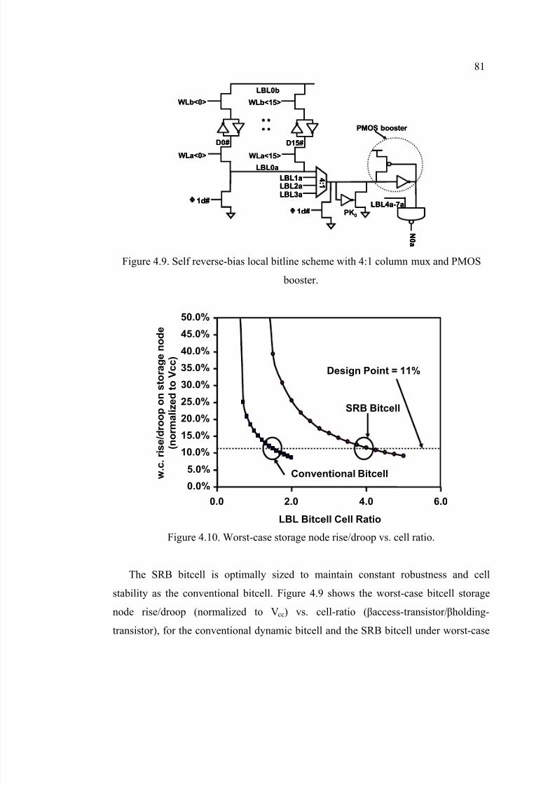
8/6/2019 Advanced Micro Architecture and Circuit Design Techniques for on-Chip Memories in CMOS Technology
http://slidepdf.com/reader/full/advanced-micro-architecture-and-circuit-design-techniques-for-on-chip-memories 97/131
81
PK0
WLb<0>
D0#
• •
• •
LBL0b
N 0 a
LBL4a-7a
LBL0a
WLa<0>
WLb<15>
D15#
WLa<15>
4 : 1
LBL1aLBL2aLBL3a
Φ1d#
PMOS booster
Φ1d# PK0
WLb<0>
D0#
• •
• •
LBL0b
N 0 a
LBL4a-7a
N 0 a
LBL4a-7a
LBL0a
WLa<0>
WLb<15>
D15#
WLa<15>
4 : 1
LBL1aLBL2aLBL3a
4 : 1
LBL1aLBL2aLBL3a
Φ1d#1d#
PMOS booster
Φ1d#1d#
Figure 4.9. Self reverse-bias local bitline scheme with 4:1 column mux and PMOS
booster.
0.0%
5.0%
10.0%
15.0%
20.0%
25.0%
30.0%
35.0%
40.0%
45.0%
50.0%
0.0 2.0 4.0 6.0
LBL Bitcell Cell Ratio
w . c . r i s e / d r o o p
o n s t o r a g e n o d e
( n o r m a l i z e d t o V c c )
Conventional Bitcell
SRB Bitcell
Design Point = 11%
Figure 4.10. Worst-case storage node rise/droop vs. cell ratio.
The SRB bitcell is optimally sized to maintain constant robustness and cell
stability as the conventional bitcell. Figure 4.9 shows the worst-case bitcell storage
node rise/droop (normalized to Vcc) vs. cell-ratio (βaccess-transistor/βholding-
transistor), for the conventional dynamic bitcell and the SRB bitcell under worst-case

8/6/2019 Advanced Micro Architecture and Circuit Design Techniques for on-Chip Memories in CMOS Technology
http://slidepdf.com/reader/full/advanced-micro-architecture-and-circuit-design-techniques-for-on-chip-memories 98/131
82
leakage conditions in the 1.2V, 130nm CMOS technology. The SRB LBL’s bitcell is
re-optimized by increasing the P/N skew of the bitcell cross-coupled inverters in order
to achieve the same worst-case storage node rise/droop target of 130mV (11% of Vcc)
as compared to the conventional dynamic LBL’s bitcell, while preserving the same
cell layout area. No additional transistors or wire-tracks are added to the SRB bitcell,
maintaining the dense layout organization of the existing L0 cache. The PMOS-
booster stage is folded into the NAND-merge layout template with <1% total layout
area penalty, demonstrating that the SRB bitline technique can be implemented as a
drop-in replacement to existing L0 caches without small area overhead.
When the word-line signals are at Vss, i.e., the SRB LBL is deselected; the access
transistors’ leakage causes the LBL to charge up towards Vcc. This induces an inherent
negative VGS reverse-bias under-drive voltage on the leakage-limiting access
transistors that in turn lowers the access transistor leakage. The LBL charges up until
it reaches a self-limiting steady-state negative VGS value. Further, body-effect on the
access transistors increases due to the VGS under-drive, which further elevates their
VTH. In addition, the drain-source voltage (VDS) for the SRB access transistors is
reduced due to the elevated source voltage, which further lowers the drain-source
leakage due to mitigated drain-induced barrier lowering (DIBL).
4.4.2. Access Transistor Operation
Figure 4.10(a)-4.10(b) shows the bitcell access transistor operation of the
conventional and SRB scheme. For a deselected conventional bitcell, the gate of the
access transistor will be at VSS, and the source of the transistor will be connected to
the data node D<15:0>, which is VSS for worst-case leakage conditions. Since the
dynamic bitline is precharged, the drain is dynamically held at VCC. Thus, the
conventional access transistor has a VGS=0 and VDS=Vcc, resulting in large
subthreshold leakage (ILEAK ) flowing through the access transistor. In the SRB case,
the access transistor gate is still connected to VSS for a deselected bitcell. However,
the data D#<15:0> and bitline nodes are swapped. The source of the access transistor
is now connected to a pre-discharged dynamic node and the drain is connected to the

8/6/2019 Advanced Micro Architecture and Circuit Design Techniques for on-Chip Memories in CMOS Technology
http://slidepdf.com/reader/full/advanced-micro-architecture-and-circuit-design-techniques-for-on-chip-memories 99/131
83
data node D#<15:0>. The worst-case leakage is when this data node D#<15:0> is at
VCC. Initially, the bitline is dynamically held at VSS, but as leakage increases, the
access transistor VGS is equivalent to a negative ΔVSRB. Figure 4.11 shows the
negative ΔVSRB development for the deselected bitline at 1.2V, 110°C, in the 130nm
CMOS technology with low-VTH access transistors. Self-limiting steady state VGS of -
220mV is reached in 40ps. Gate-oxide overstress is avoided since worst-case voltage
across any of the access transistor terminals is still Δ|Vcc| - this is especially important
in the context of process cost savings, since the technology does not have to support
multiple gate oxide thicknesses.
(a) (b)
S=VSS
G=VSS
D=VCC
+
-
VGS=0
Ileak
Bitline
S=VSRB
G=VSS
D=VCC
+
-
VGS=-ΔVSRB
Bitline
Ileak
S=VSS
G=VSS
D=VCC
+
-
VGS=0
Ileak
Bitline
S=VSRB
G=VSS
D=VCC
+
-
VGS=-ΔVSRB
Bitline
Ileak
Figure 4.11. Access transistor operation (a) Conventional (b) Self reverse-bias.
Time (ps)
V o l t a g e ( V )
1.2Φ1d#
LBL0a
Vcc = 1.2V, 110°C
0.9
0.6
0.3
300
0 60 90 120 150 180
Tsettle = 40ps
VGS = -220mV
Time (ps)
V o l t a g e ( V )
1.2Φ1d#
LBL0a
Vcc = 1.2V, 110°C
0.9
0.6
0.3
300
0 60 90 120 150 180
Tsettle = 40ps
VGS = -220mV
Figure 4.12. Timing operation of self reverse-bias scheme achieving VGS=–220mV.

8/6/2019 Advanced Micro Architecture and Circuit Design Techniques for on-Chip Memories in CMOS Technology
http://slidepdf.com/reader/full/advanced-micro-architecture-and-circuit-design-techniques-for-on-chip-memories 100/131
84
4.4.3. Bitline Leakage Impact
To evaluate the bitline leakage benefit of SRB technique, we first measure this
impact on 130nm transistors. Figure 4.12 shows device-level measurements across
several dies of normalized active leakage reduction achieved on low-VTH NMOS
transistors with gate-source under-drive in 130nm technology at 1.2V, 80°C (due to
wafer-oxidation limits, maximum test temperature is stabilized at 80°C instead of
110°C), for transistor dimensions comparable to the bitline NMOS access transistors.
1.E+00
1.E+01
1.E+02
1.E+03
1.E+04
1.E+05
-0.3 -0.2 -0.1 0.0 0.1 0.2 0.3
Access Transistor VGS (V)
N o r m a l i z e d S - D L e a k a
g e
Conventional
This work 72x
1.E+00
1.E+01
1.E+02
1.E+03
1.E+04
1.E+05
-0.3 -0.2 -0.1 0.0 0.1 0.2 0.3
Access Transistor VGS (V)
N o r m a l i z e d S - D L e a k a
g e
Conventional
This work 72x
VG = VB = 0, VD = 1.2V, 80°C
T e s t R o w s 2
T e s t R o w s 1
T e s t R o w s 2
T e s t R o w s 1
Figure 4.13. 130nm leakage testchip rows and measurements.
Similar to the leaking NMOS access transistors of a deselected bitline, the gate
voltage (VG) and body voltage (VB) are setup at GND and the drain voltage (VD) is
setup at Vcc. Leakage is measured between the drain terminal and GND. In a
conventional bitline the source voltage would be at GND, whereas in the SRB bitline
the source voltage rises to 220mV at 1.2V. As the source voltage increases from GND
to 220mV, the gate-source under-drive (VGS) changes from 0 (conventional dynamic
bitline situation) to –220mV (SRB bitline situation). At the same time, drain-source
voltage also decreases from Vcc to Vcc-220mV, and the body-effect is increased since
VBS = -220mV at this condition. Note that the drain junction diode leakage still exists.
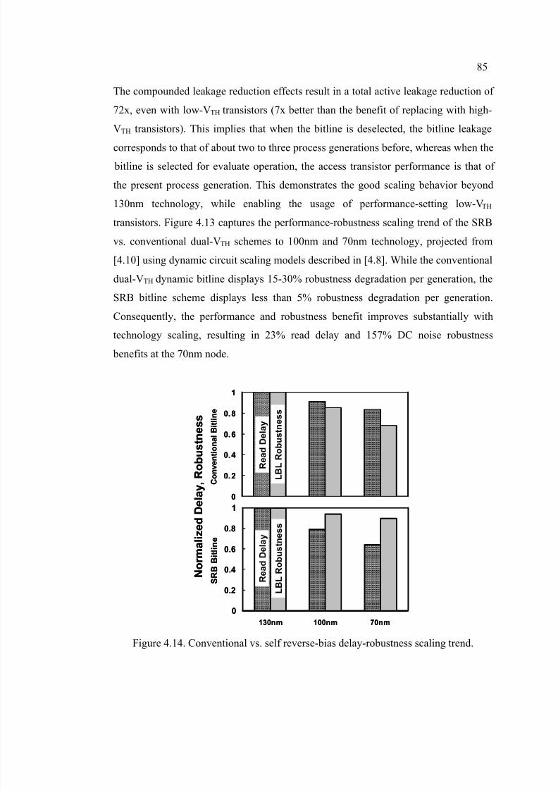
8/6/2019 Advanced Micro Architecture and Circuit Design Techniques for on-Chip Memories in CMOS Technology
http://slidepdf.com/reader/full/advanced-micro-architecture-and-circuit-design-techniques-for-on-chip-memories 101/131
85
The compounded leakage reduction effects result in a total active leakage reduction of
72x, even with low-VTH transistors (7x better than the benefit of replacing with high-
VTH transistors). This implies that when the bitline is deselected, the bitline leakage
corresponds to that of about two to three process generations before, whereas when the
bitline is selected for evaluate operation, the access transistor performance is that of
the present process generation. This demonstrates the good scaling behavior beyond
130nm technology, while enabling the usage of performance-setting low-VTH
transistors. Figure 4.13 captures the performance-robustness scaling trend of the SRB
vs. conventional dual-VTH schemes to 100nm and 70nm technology, projected from
[4.10] using dynamic circuit scaling models described in [4.8]. While the conventional
dual-VTH dynamic bitline displays 15-30% robustness degradation per generation, the
SRB bitline scheme displays less than 5% robustness degradation per generation.
Consequently, the performance and robustness benefit improves substantially with
technology scaling, resulting in 23% read delay and 157% DC noise robustness
benefits at the 70nm node.
0
0.2
0.4
0.6
0.8
1
130nm 100nm 70nm
S R B B i t l i n e
R e a d D e l a y
L B L R o b u
s t n e s s
0
0.2
0.4
0.6
0.8
1
C o n v e n t i o n a l B i t l i n
e
R e a d D e l a y
L B L R o b u s t n e s s
N o r m
a l i z e d D e l a y , R o b u s t n e s s
0
0.2
0.4
0.6
0.8
1
130nm 100nm 70nm
S R B B i t l i n e
R e a d D e l a y
L B L R o b u
s t n e s s
0
0.2
0.4
0.6
0.8
1
C o n v e n t i o n a l B i t l i n
e
R e a d D e l a y
L B L R o b u s t n e s s
N o r m
a l i z e d D e l a y , R o b u s t n e s s
Figure 4.14. Conventional vs. self reverse-bias delay-robustness scaling trend.

8/6/2019 Advanced Micro Architecture and Circuit Design Techniques for on-Chip Memories in CMOS Technology
http://slidepdf.com/reader/full/advanced-micro-architecture-and-circuit-design-techniques-for-on-chip-memories 102/131
86
4.4.4. Performance Impact
There are two main factors that degrade the SRB bitline evaluate performance
compared to conventional dual-VTH dynamic bitlines. Firstly, the source follower
NMOS pullup operation of the access transistors is a self shut-off mechanism and
hence degrades the transistor drive progressively until the bitline pulls up to Vcc-VTH.
Secondly, a PMOS-booster stage is inserted between the LBL and the static NAND-
merge stage, i.e., an additional stage of delay compared to the conventional dual-VTH
dynamic bitline. Both these delay-degrading penalties are more than compensated by
three delay-improving circuit features enabled by this technique:
• Low-VTH access transistor usage and 40% downsized bitline keepers, which
significantly mitigates bitline contention during evaluate operation.
• Improved NAND-merge input edge-rates due to bitline capacitance decoupled
by the PMOS-booster stage, resulting in a speedup of the subsequent GBL gates.
• Bitline and word-line signals in the SRB scheme transition in same direction,
reducing the miller-switched capacitance load on word-line drivers.
These factors result in the low-VTH SRB LBL technique achieving faster read
performance than the conventional dual-VTH dynamic LBL technique.
4.5. Performance-Robustness Comparisons and Discussion
4.5.1. Performance Comparisons
The conventional dual-VTH dynamic and the low-VTH SRB L0 caches are all
optimally sized and simulated in the 130nm technology at 1.2V, 110°C. In all cases, a
Lagrange-multiplier based quadratic optimizer is used for optimal transistor sizing to
make the comparisons fair and to achieve a robust optima centered around the “knee”
of their respective energy-delay curves [4.12]. All simulations include full layoutextracted back-annotated device and interconnect parasitics. Performance and energy
simulations are conducted in the nominal process leakage corner. All robustness
comparisons are performed at the worst-case process leakage corner, since full
functionality is required at this corner.

8/6/2019 Advanced Micro Architecture and Circuit Design Techniques for on-Chip Memories in CMOS Technology
http://slidepdf.com/reader/full/advanced-micro-architecture-and-circuit-design-techniques-for-on-chip-memories 103/131
8/6/2019 Advanced Micro Architecture and Circuit Design Techniques for on-Chip Memories in CMOS Technology
http://slidepdf.com/reader/full/advanced-micro-architecture-and-circuit-design-techniques-for-on-chip-memories 104/131
88
Table 4.2. Delay and Energy Comparison (1.2V,110°C).
157ps162ps
Write
Delay
26.88pJ28.14pJ
247ps220ps
ConventionalThis work
Energy/transitionRead
DelayLBL Scheme
157ps162ps
Write
Delay
26.88pJ28.14pJ
247ps220ps
ConventionalThis work
Energy/transitionRead
DelayLBL Scheme
4.5.2. Robustness Comparisons
To compare DC robustness of the LBL techniques, worst-case word-line DC noise
conditions are setup for each. For the dual-VTH dynamic LBL, bitcell data inputs
D<15:0> are set to Vss. For the SRB LBL, bitcell data# inputs D#<15:0> are set to
Vcc. This condition enables any noise on word-line signals to propagate onto the LBL
and trigger a false discharge. DC noise offsetted above Vss is applied on all the word-
line inputs WL<15:0>, representing input-referenced ground bounce and coupling
noise propagated from the previous word-line driver stages. DC robustness is
evaluated as unity-gain noise margin at the output of the LBL-merge 2-input NAND
gate normalized to Vcc. With no DC noise applied on the word-line inputs, the steady-
state DC droop of the conventional dual-VTH dynamic bitline is 350mV at 1.2V,
110°C at the worst-case process leakage corner (Table 4.3). The SRB LBL rises to a
steady-state DC value of 220mV, 37% lower than the conventional dual-VTH bitline
despite using low-VTH access transistors. Due to the inherent negative VGS on the
access transistors of the SRB technique, the input noise has to reach a minimum of |-
VGS| before the access transistors are triggered on. Further, the PMOS booster stage
offers a stage of noise attenuation before the applied noise manifests itself at the input
of the 2-input static NAND-merge stage. These factors result in the SRB LBL
demonstrating 104% (2x) higher DC robustness than the dual-VTH scheme.
Table 4.3. DC Robustness and LBL Droop/Rise Comparison (1.2V,110°C).
350mV
220mV
0.114
0.233
Conventional
This work
LBL droop/riseDC robustness
(DC noise margin/Vcc)LBL Scheme
350mV
220mV
0.114
0.233
Conventional
This work
LBL droop/riseDC robustness
(DC noise margin/Vcc)LBL Scheme

8/6/2019 Advanced Micro Architecture and Circuit Design Techniques for on-Chip Memories in CMOS Technology
http://slidepdf.com/reader/full/advanced-micro-architecture-and-circuit-design-techniques-for-on-chip-memories 105/131
89
4.5.3. Robustness-Delay Tradeoff
As mentioned in previous section, the bitline keeper transistor can be upsized to
trade off delay for better robustness on all LBL schemes. Figure 4.14 shows the LBL
DC robustness vs. the LBL evaluate delay trade-off for keeper upsizing beyond their
respective baseline sizes for the conventional and SRB LBL schemes. The SRB
scheme extends the robustness vs. delay curve beyond the conventional dynamic
bitline scheme, due to the inherently higher robustness at smaller keeper sizes. At the
“knee” of the conventional dynamic LBL’s delay vs. robustness curve, a 34% increase
in DC robustness is achieved for a 26% delay penalty. As the keeper size, and hence
robustness, is increased, the delay penalty becomes more evident and a 17% increase
in robustness costs a 34% increase in delay. The higher robustness-delay slope occurs
when the keeper strength increase begins to strongly contend with the evaluation
performance. In the SRB scheme, the optima occurs substantially beyond the
conventional dynamic LBL’s robustness-delay curve and begins to slope at a much
higher robustness level – both of these enable a smaller baseline keeper size to meet
target noise margin constraints. Across a wide range of bitline keeper sizes, the
proposed SRB technique sustains both robustness and speed advantages over the
conventional dynamic dual-VTH technique.
0.00
0.20
0.40
0.60
0.80
1.00
1.20
0.00 0.20 0.40 0.60 0.80 1.00 1.20
Normalized DC Noise Robustness
N o r m a l i z e d L B L D e l a y
Conventional
SRB
K e e p
e r U p s i z i n
g
Figure 4.15. LBL robustness vs. delay trade-off.
8/6/2019 Advanced Micro Architecture and Circuit Design Techniques for on-Chip Memories in CMOS Technology
http://slidepdf.com/reader/full/advanced-micro-architecture-and-circuit-design-techniques-for-on-chip-memories 106/131
90
4.6. Conclusion
A leakage-tolerant self reverse-bias bitline technique is described that establishes
negative gate-source under-drive on the leakage-limiting access transistors without
distributing additional supply/bias voltages, pre-conditioning control signals, or gate-
oxide overstress. Using this technique, we have presented a 4.5GHz 2-read, 1-write
ported 32KB L0 cache in 1.2V, 130nm technology. 11% faster read delay with a
simultaneous 2x DC noise robustness is achieved when compared to a dual-VTH bitline
scheme optimized for high-performance. The aggressive bitline active leakage
reduction enabled 16 bitcells/bitline, low-VTH usage, and 40% keeper downsizing, and
demonstrates good performance-robustness scaling trend to 100nm and 70nm
technologies.

8/6/2019 Advanced Micro Architecture and Circuit Design Techniques for on-Chip Memories in CMOS Technology
http://slidepdf.com/reader/full/advanced-micro-architecture-and-circuit-design-techniques-for-on-chip-memories 107/131
91
References
[4.1] R. Krishnamurthy, et al., “A 130nm 6GHz 256x32b leakage-tolerant register
file,” IEEE Journal Solid State Circuits, vol. 37, pp. 624-632, May 2002.
[4.2] H. Tanaka, et al., “A precise on-chip voltage generator for a gigascale DRAMwith a negative word-line scheme,” IEEE Journal Solid-State Circuits, vol. 34,
pp. 1084-1090, Aug. 1999.
[4.3] H. Kawaguchi, et al., “Dynamic leakage cut-off scheme for low-voltageSRAMs,” in Symposium VLSI Circuits Digest Technical Papers, June 1998,
pp. 140-141.
[4.4] T. Kuroda, et al., “A 0.9V 150MHz 10mW 4mm2
2-D discrete cosine
transform core processor with variable threshold voltage scheme,” IEEE Journal Solid-State Circuits, vol. 31, pp. 1770-1779, Nov. 1996.
[4.5] K. Agawa, et al., “A bitline leakage compensation scheme for low-voltage
SRAMs,” IEEE Journal Solid-State Circuits, vol. 36, pp. 726-734, May 2001.
[4.6] G. Balamurugan, et al., “A twin-transistor noise-tolerant dynamic circuit
technique,” IEEE Journal Solid-State Circuits, vol. 36, pp. 273-280, Feb.
2001.
[4.7] S. Hsu, et al., “A 4.5GHz 130nm 32KB L0 cache with a self reverse-bias
scheme,” in Symposium VLSI Circuits Digest Technical Papers, June 2002, pp.48-49.
[4.8] M. Anders, et al., “Robustness of sub-70nm dynamic circuits: analyticaltechniques and scaling trends,” in Symposium VLSI Circuits Digest Technical
Papers, June 2001, pp. 23-24.
[4.9] A. Alvandpour, et al., “A sub-130-nm conditional keeper technique,” IEEE
Journal Solid-State Circuits, vol. 37, pp. 633-638, May 2002.
[4.10] S. Tyagi, et al., “A 130nm generation logic technology featuring 70nm
transistors, dual-Vt transistors and 6 layers of Cu interconnects,” in International Electron Devices Meeting Technical Digest , Dec. 2000, pp. 567-
570.
[4.11] R. Krishnamurthy, et al., “High-performance and low-power challenges for
sub-70nm microprocessor circuits,” in Custom Integrated Circuits Conference
Digest Technical Papers, May 2002.

8/6/2019 Advanced Micro Architecture and Circuit Design Techniques for on-Chip Memories in CMOS Technology
http://slidepdf.com/reader/full/advanced-micro-architecture-and-circuit-design-techniques-for-on-chip-memories 108/131
92
[4.12] G. Anderson, et al., “OPTIM2 v. 1.5.1 user’s guide,” August 2001.

8/6/2019 Advanced Micro Architecture and Circuit Design Techniques for on-Chip Memories in CMOS Technology
http://slidepdf.com/reader/full/advanced-micro-architecture-and-circuit-design-techniques-for-on-chip-memories 109/131
93
AN 8.8GHz 198mW 16x64b 1R/1W VARIATION-TOLERANT
REGISTER FILE IN 65nm CMOS
Steven K. Hsu, Amit Agarwal, Mark Anders, Sanu Mathew
Ram K. Krishnamurthy, Shekhar Borkar
International Solid-State Circuits Conference Digest Technical PapersFeb. 2006, pp. 448-449

8/6/2019 Advanced Micro Architecture and Circuit Design Techniques for on-Chip Memories in CMOS Technology
http://slidepdf.com/reader/full/advanced-micro-architecture-and-circuit-design-techniques-for-on-chip-memories 110/131
94
5. MULTI-STRENGTH KEEPER REGISTER FILES
5.1. Introduction
Wide bit-width (≥ 64b) single read/write ported register files are essential building
blocks in high-performance superscalar microprocessors demanding single-cycle
latency/throughput and dense organization. Significant process, supply voltage, and
temperature (PVT) induced variations in transistor leakage limit the performance and
robustness of wide dynamic register file bitlines. A 16x64b single read/write ported
variation-tolerant register file with single cycle read/write latency and throughput is
fabricated in 65nm CMOS technology [5.1]. Operating at 8.8GHz, it consumes
198mW (measured at 1.2V, 50°C) (Figure 5.7). Fused static decode and 64b dynamic
array read within a single cycle, split decoder with PVT/burn-in tolerant keeper
compensation, leakage-tolerant split wordline architecture, and shared twin memory
cell (TMC) topology enable a dense layout occupying 0.017mm2
while simultaneously
achieving (i) wide range of PVT operating points across slow-fast corners, 0.5-1.4V
and 25-110°C, (ii) low active leakage power of 25mW with optimal non-minimum
channel length usage, (iii) high noise immunity with an ultra low bitline noise droop
<8mV, (iv) scalable register file performance up to 10.1GHz, 273mW measured at
1.4V, 50°C, and (v) low-voltage mode performance of 300MHz, 1.3mW measured at
500mV, 50°C. Simultaneous supply/temperature scaling enables 13% total power
reduction at iso-frequency (measured at 8.8GHz, 1.16V, 25°C) or 9% higher
performance at iso-power (measured at 9.6GHz, 1.25V, 25°C).
5.2.Register File Design
Figure 5.1 shows the organization of the single-cycle 1-read, 1-write ported
register file tile, consisting of 16-entries x 64-bits. This design can be scaled to a larger
register file memory array by replication [5.2]. A 2Ф 50% duty-cycle clocking plan
allows seamless time-borrowing at the address input and data output interfaces. In the
first phase (Ф1) of the cycle, a fully static one-hot 4b address decoder generates the
read/write select wordlines. Clocked NAND gates convert the static decoder outputs
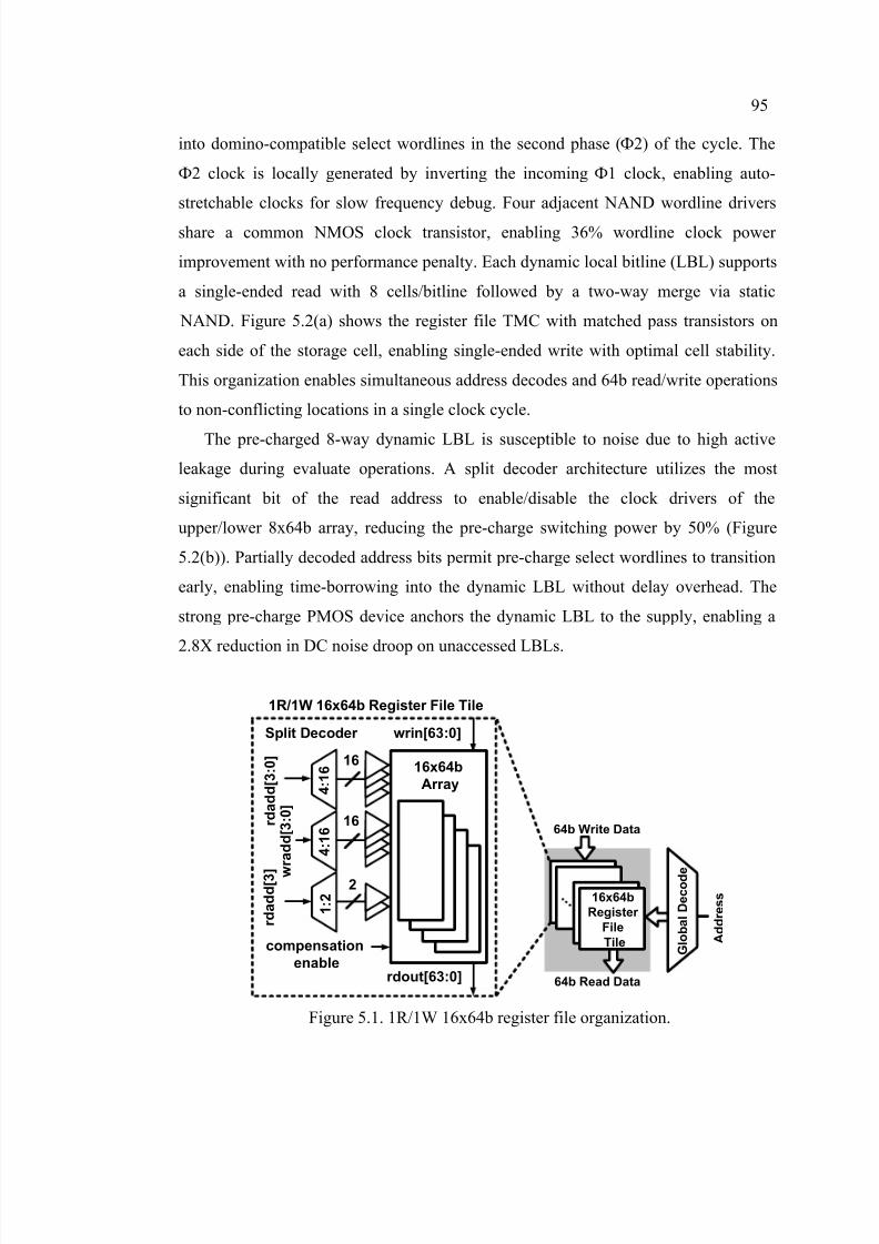
8/6/2019 Advanced Micro Architecture and Circuit Design Techniques for on-Chip Memories in CMOS Technology
http://slidepdf.com/reader/full/advanced-micro-architecture-and-circuit-design-techniques-for-on-chip-memories 111/131
95
into domino-compatible select wordlines in the second phase (Ф2) of the cycle. The
Ф2 clock is locally generated by inverting the incoming Ф1 clock, enabling auto-
stretchable clocks for slow frequency debug. Four adjacent NAND wordline drivers
share a common NMOS clock transistor, enabling 36% wordline clock power
improvement with no performance penalty. Each dynamic local bitline (LBL) supports
a single-ended read with 8 cells/bitline followed by a two-way merge via static
NAND. Figure 5.2(a) shows the register file TMC with matched pass transistors on
each side of the storage cell, enabling single-ended write with optimal cell stability.
This organization enables simultaneous address decodes and 64b read/write operations
to non-conflicting locations in a single clock cycle.
The pre-charged 8-way dynamic LBL is susceptible to noise due to high active
leakage during evaluate operations. A split decoder architecture utilizes the most
significant bit of the read address to enable/disable the clock drivers of the
upper/lower 8x64b array, reducing the pre-charge switching power by 50% (Figure
5.2(b)). Partially decoded address bits permit pre-charge select wordlines to transition
early, enabling time-borrowing into the dynamic LBL without delay overhead. The
strong pre-charge PMOS device anchors the dynamic LBL to the supply, enabling a
2.8X reduction in DC noise droop on unaccessed LBLs.
16x64b
Array
r d a d d [ 3 : 0 ]
rdout[63:0]
r d a d d [ 3 ]
4 : 1 6
1 : 2
16
2
4 : 1 6
16
w
r a d d [ 3 : 0 ]
compensation
enable
Split Decoder wrin[63:0]
1R/1W 16x64b Register File Tile
16x64b
Register
File
Tile G l o b a l D e c o d e
64b Write Data
64b Read Data
A d d r e s s
Figure 5.1. 1R/1W 16x64b register file organization.

8/6/2019 Advanced Micro Architecture and Circuit Design Techniques for on-Chip Memories in CMOS Technology
http://slidepdf.com/reader/full/advanced-micro-architecture-and-circuit-design-techniques-for-on-chip-memories 112/131
96
1 . 6 2 5 µ m
5.09µm
Noise Suppression Inverter Non-minimum Channel LengthNon-minimum Channel Length
* *
rdwl
wrwl
lbl[0] wrin[0] wrin[1] lbl[1]
*
* *
*
Figure 5.2. Twin memory cell (TMC) topology and layout.
rdadd[3]
Read Decoder
Split Decoder
rdwlen
prewlen
rdadd[3:0]
rdadd[0]Shared Stack Node
rdwl
prewlb
rdadd[1]
rdadd[2]
rdadd[3]
4X
2X
Shared Stack Node
Figure 5.3. Decoder organization with shared stack node wordline drivers.

8/6/2019 Advanced Micro Architecture and Circuit Design Techniques for on-Chip Memories in CMOS Technology
http://slidepdf.com/reader/full/advanced-micro-architecture-and-circuit-design-techniques-for-on-chip-memories 113/131
97
*
* ** *
* **
vss
Conventional Wordline
Split Wordline
rdwl
vss
rdwl
rdwlen
Twin Memory Cell
Non-minimum Channel Length
Noise Suppression Inverter
rdwlen
*
Figure 5.4. Wordline circuit topologies.
A split wordline architecture distributes the wordline driver inverter across the
entire memory array, suppressing input voltage noise offset on the sensitive dynamic
pull-down inputs (Figure 5.2(c)). This noise suppression inverter, locally embedded in
the TMC, enables a 35% increase in LBL DC noise robustness at the same
performance. Wordline noise suppression inverters and wire tracks are shared between
two bitcells to minimize total area, providing a dense TMC layout occupying 5.09µm
x 1.625µm (Figure 5.2(a)). Optimal non-minimum channel lengths [5.3] in the storage
cell cross coupled inverters and read access transistors reduce TMC active leakage by
3.7X compared to the conventional bitcell implementation.
A NAND2-based PVT/burn-in keeper with 1-bit enable provides PVT
compensation on all bitlines across slow-fast corners, 0.5-1.4V, and 25-110°C [5.4].
Across this PVT range, transistor leakage varies by 4 orders of magnitude. Comparedto a 2PMOS-based keeper [5.5], this implementation enables a 39% reduction in total
compensation circuit transistor width (1µm LBL pulldown width, 8% keeper) at
equivalent performance (Figure 5.3(a)). With compensation turned ON, optimized
keeper sizes improve the DC noise robustness of fast dies by 27% to meet the target
noise margin constraints, resulting in a worst-case LBL dynamic node droop ≥ 8mV.

8/6/2019 Advanced Micro Architecture and Circuit Design Techniques for on-Chip Memories in CMOS Technology
http://slidepdf.com/reader/full/advanced-micro-architecture-and-circuit-design-techniques-for-on-chip-memories 114/131
98
Turning OFF the compensation on the slow dies trades surplus robustness for higher
performance (8% down to 4% keeper). This optimization on slow dies achieves a
measured 10% delay improvement and tighter delay/robustness distributions across
slow-fast dies (Figure 5.3(b)).
0.00
0.50
1.00
1.50
2.00
2.50
3.00
3.50
4.00
0.40 0.60 0.80 1.00 1.20 1.40
LBL Pulldown Transistor Width (μm)
T o t a l C o
m p e n s a t i o n C i r c u i t
T r a n s
i s t o r W i d t h ( μ m )
2PMOS
NAND2
39% less
Design Point
65nm CMOS
enable
2PMOS
enable
NAND2
Figure 5.5. Keeper compensation circuits and comparison.
0.50.95
1.4
20
65
1100
0.5
1
Voltage (V)
Slow
Temp. (°C)
L e a k
a g e
0.50.95
1.4
20
65
1100
0.5
1
Voltage (V)
Typical
Temp. (°C)
L e a k a g e
0.50.95
1.4
20
65
1100
0.5
1
Voltage (V)
Fast
Temp. (°C)
L e a k a g e
Compensation ON
27% Higher Robustness
Compensation OFF
10% Delay Improvement
Figure 5.6. Process, voltage, temperature leakage compensation across slow-fast
dies.
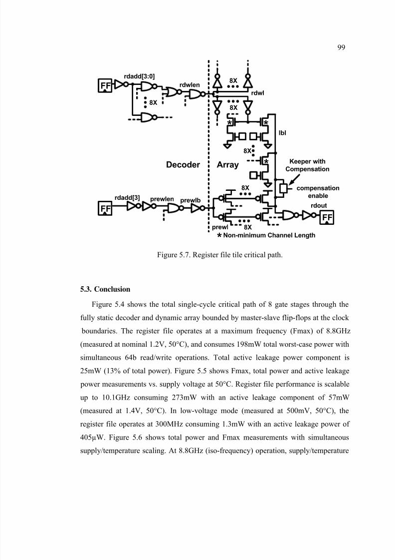
8/6/2019 Advanced Micro Architecture and Circuit Design Techniques for on-Chip Memories in CMOS Technology
http://slidepdf.com/reader/full/advanced-micro-architecture-and-circuit-design-techniques-for-on-chip-memories 115/131
99
FF
FF
FF
8X8X
8X
Decoder Array
8X
8X
8X
* *
*
rdadd[3]
rdadd[3:0]
rdwl
lbl
rdout
prewl
Keeper with
Compensation
Non-minimum Channel Length
rdwlen
prewlen prewlb
compensation
enable
*
Figure 5.7. Register file tile critical path.
5.3. Conclusion
Figure 5.4 shows the total single-cycle critical path of 8 gate stages through the
fully static decoder and dynamic array bounded by master-slave flip-flops at the clock
boundaries. The register file operates at a maximum frequency (Fmax) of 8.8GHz
(measured at nominal 1.2V, 50°C), and consumes 198mW total worst-case power with
simultaneous 64b read/write operations. Total active leakage power component is
25mW (13% of total power). Figure 5.5 shows Fmax, total power and active leakage
power measurements vs. supply voltage at 50°C. Register file performance is scalable
up to 10.1GHz consuming 273mW with an active leakage component of 57mW
(measured at 1.4V, 50°C). In low-voltage mode (measured at 500mV, 50°C), the
register file operates at 300MHz consuming 1.3mW with an active leakage power of
405µW. Figure 5.6 shows total power and Fmax measurements with simultaneous
supply/temperature scaling. At 8.8GHz (iso-frequency) operation, supply/temperature

8/6/2019 Advanced Micro Architecture and Circuit Design Techniques for on-Chip Memories in CMOS Technology
http://slidepdf.com/reader/full/advanced-micro-architecture-and-circuit-design-techniques-for-on-chip-memories 116/131
100
scaling to 1.16V, 25°C reduces total power to 172mW (13% reduction). At 1.25V,
25°C operation, Fmax improves to 9.6GHz (9% higher) while maintaining the same
total power. PVT compensation is turned on at elevated temperature (110°C) to enable
fully functional operation at iso-frequency (measured at 1.4V, 8.8GHz, 285mW) or
iso-power consumption (measured at 1.24V, 7.9GHz, 198mW).
0.0
2.0
4.0
6.0
8.0
10.0
12.0
0.40 0.62 0.84 1.06 1.28 1.50Supply Voltage (V)
M a x i m u m
F r e q u e n c y
( G
H z )
0
50
100
150
200
250
300
T o t a l P o
w e r ( m W )
65nm CMOS, 50°C
1.2V
0.0
2.0
4.0
6.0
8.0
10.0
12.0
0.40 0.62 0.84 1.06 1.28 1.50Supply Voltage (V)
M a x i m u m
F r e q u e n c y
( G
H z )
0
50
100
150
200
250
300
T o t a l P o
w e r ( m W )
65nm CMOS, 50°C
1.2V
Figure 5.8. Frequency, total power measurements vs. supply.
0
10
20
30
40
50
60
0.40 0.62 0.84 1.06 1.28 1.50Supply Voltage (V)
L
e a k a g e P o w e r ( m W )
65nm CMOS, 50°C
1.2V
Figure 5.9. Leakage power measurements vs. supply.

8/6/2019 Advanced Micro Architecture and Circuit Design Techniques for on-Chip Memories in CMOS Technology
http://slidepdf.com/reader/full/advanced-micro-architecture-and-circuit-design-techniques-for-on-chip-memories 117/131
101
0
50
100
150
200
250
300
350
400
25 50 110Temperature (°C)
T o t a l P o w e r ( m W )
Iso-frequency = 8.8GHz
13%
285mW
1.40V
198mW1.20V172mW
1.16V44%
65nm CMOS
c o m p .
O F F
c o m p .
O F F
c o m p .
O N
0
50
100
150
200
250
300
350
400
25 50 110Temperature (°C)
T o t a l P o w e r ( m W )
Iso-frequency = 8.8GHz
13%
285mW
1.40V
198mW1.20V172mW
1.16V44%
65nm CMOS
c o m p .
O F F
c o m p .
O F F
c o m p .
O N
Figure 5.10. Total power with simultaneous supply/temperature scaling.
6
6.5
7
7.5
8
8.5
9
9.5
10
10.5
11
25 50 110Temperature (°C)
M a
x i m u m
F r e q u e n c y
( G H z
)Iso-power = 198mW
8.8GHz1.20V
7.9GHz
1.24V
9.6GHz
1.25V
9%
10%
65nm CMOS
c o m
p .
O F F
c o m
p .
O F F
c o m
p .
O N
6
6.5
7
7.5
8
8.5
9
9.5
10
10.5
11
25 50 110Temperature (°C)
M a
x i m u m
F r e q u e n c y
( G H z
)
8.8GHz1.20V
7.9GHz
1.24V
9.6GHz
1.25V
Iso-power = 198mW
9%
10%
65nm CMOS
c o m
p .
O F F
c o m
p .
O F F
c o m
p .
O N
Figure 5.11. Fmax measurements with simultaneous supply/temperature scaling.
16x64b Register File
Array
Figure 5.12. Register file die microphotograph.

8/6/2019 Advanced Micro Architecture and Circuit Design Techniques for on-Chip Memories in CMOS Technology
http://slidepdf.com/reader/full/advanced-micro-architecture-and-circuit-design-techniques-for-on-chip-memories 118/131
102
References
[5.1] P. Bai, et al., “A 65nm logic technology featuring 35nm gate lengths, enhance
channel strain, 8 Cu interconnect layers, low-k ILD and 0.57um2
SRAM cell,”
in International Electron Devices Meeting Technical Digest , Dec. 2004, pp.
657-660.
[5.2] J. Miller, et al., “A 16 GB/s, 0.18 μm cache tile for integrated L2 caches from
256 KB to 2 MB,” in Symposium VLSI Circuits Digest Technical Papers, June2000, pp. 228-231.
[5.3] E. Fetzer, et al., “The multi-threaded, parity-protected 128-word register fileson a dual-core Itanium-family processor,” in International Solid-State Circuits
Conference Digest Technical Papers, Feb. 2005, pp. 382-383.
[5.4] A. Alvandpour, et al., “A burn-in tolerant dynamic circuit technique,” inCustom Integrated Circuits Conference Digest Technical Papers, Sept. 2002,
pp. 81-84.
[5.5] D. Stasiak, et al., “A 2nd
generation 440ps SOI 64b adder,” in International
Solid-State Circuits Conference Digest Technical Papers, Feb. 2000, pp. 288-
289.
8/6/2019 Advanced Micro Architecture and Circuit Design Techniques for on-Chip Memories in CMOS Technology
http://slidepdf.com/reader/full/advanced-micro-architecture-and-circuit-design-techniques-for-on-chip-memories 119/131
103
6. CONCLUSION
As modern superscalar microprocessors become wider to exploit instruction level
parallelism, the multi-ported register file is becoming a more critical source of on-chip
memory bottleneck. Large-signals multi-ported register files contain the most critical
speed paths, limiting the microprocessor frequency and consuming one of the largest
percentages of power at ~25%. A large variety of register files in a state-of-the-art
microprocessor consumes a significant amount of area, resulting in some of the hottest
spots, especially near the execution core. As technology scales, increased leakage
degrades the robustness of dynamic circuits, requiring increased keeper sizes in
register file local/global bitlines to maintain functionality. This chapter will review
key microarchitecture and circuit contributions that improve register file performance,
power, area, and robustness. This chapter also will highlight additional future research
directions related to register file design.
6.1.Thesis Contribution
The key contributions and results of this thesis are summarized below.
Chapter 2 analyzes multi-banking, multi-frequency, and multi-bit width register
files to reduce power and lower area. This chapter proposes the concept of using
multi-banking with multi-frequency to take the advantages of both techniques, while
mitigating the disadvantages of each. Comparisons of integer register files for 4-wide
to 8-wide issue machines in 65nm CMOS show that using both multi-banking and
multi-frequency techniques show good promise in reducing area, improving
frequency, and lowering active and leakage power for future multi-ported register files
in wide-issue machines. This chapter also proposes an area, frequency, and power
(active and leakage) model for multi-ported power models. Unlike previous models,
the proposed model contains an estimation of the leakage component, which is
extremely important for future leakage-dominant register files.
Chapter 3 analyzes and proposes the concept of physical locality, and introduces
multi-access register files with variable cycle time latencies to improve the

8/6/2019 Advanced Micro Architecture and Circuit Design Techniques for on-Chip Memories in CMOS Technology
http://slidepdf.com/reader/full/advanced-micro-architecture-and-circuit-design-techniques-for-on-chip-memories 120/131
104
performance of the processor [6.1]. Physical locality is the location of the physical
layout of the circuits. Variable cycle time latencies depend on the physical locality to
improve the performance of loops containing dependent instructions. Data stored
physically closer to the output is accessed more quickly, since the data has better
physical locality. Furthermore, the chapter proposes a method to re-configure the
address decoding to take further advantage of the asymmetric access time for the
physical register file. Using this proposed scheme achieves a significant recovery of
the IPC lost. Variable multi-cycle access memories shows good scaling trend as the
microprocessor’s pipeline is further deepened.
Chapter 4 analyzes and proposes a leakage-tolerant self reverse-bias bitline
technique that establishes negative gate-source under-drive on the leakage-limiting
low-VTH access transistors [6.2] [6.3]. This novel circuit topology uses leaky low-VTH
devices in a multi-threshold process to improve robustness and lower delay. The
increased robustness is a result of the negative gate-sour bias on access transistors,
while the delay improvement is a result of the keeper downsizing. This technique
shows good promise for delay-robustness trade-offs in future scaled technologies with
leaky low-VTH devices, improving the delay through reduced keeper contention and
improving the robustness using negative gate-source under-drive.Chapter 5 analyzes and proposes a multi-strength keeper and several other low-
power/noise-tolerant techniques for a variation-tolerant register file in 65nm CMOS
[6.4]. Significant process, supply voltage, and temperature (PVT) induced variations
in transistor leakage limit the performance and robustness of wide dynamic register
file bitlines. The low-power/noise-tolerant techniques include the following: fused
static decode and array read, split decoder with PVT/burn-in compensation, leakage-
tolerant split wordline architecture, and shared twin memory cell topology.
6.2. Future Work
On-chip memory will continue to be an active research area since many tradeoffs
exist between performance, power, area, and robustness at all levels of the design
optimization hierarchy. The research techniques proposed and discussed in this thesis

8/6/2019 Advanced Micro Architecture and Circuit Design Techniques for on-Chip Memories in CMOS Technology
http://slidepdf.com/reader/full/advanced-micro-architecture-and-circuit-design-techniques-for-on-chip-memories 121/131
105
can be used in combination with each other and future other approaches to provide
further gains.
Simultaneous multi-threading exploits both instruction level parallelism and
thread-level parallelism by issuing instructions from different threads in the same
cycle [6.5]. Multi-threaded microprocessors contain the hardware state of each thread;
therefore, the register files need to contain an extra storage element for each thread
[6.6]-[6.8]. The concept of a “window” was first published as a three-dimensional
register file having the ability to perform a context switch [6.9]. Since highly multi-
ported register file cells are wire dominated, the extra storage cells are folded into the
layout without extra penalty. Future microprocessors will incorporate multi-threads to
improve the utilization of execution units; therefore, future register files will require
dense layout with minimal area overhead for additional threads, and high-speed/low-
power thread or context switch capability.
On-chip memory susceptibility to soft errors and transient faults can affect
reliability, resulting in the use of error correction codes (ECC) in large-level caches
[6.10]-[6.12]. Use of ECC codes to protect against silent data corruption in memories
has been a common practice. Particularly in server class microprocessors, on-chip
memory protection against soft errors and transient faults ensures a reliablecomponent. Today, modern integer and floating point register files for server class
microprocessors are implementing parity, to protect against soft errors and transient
faults since adding a thread effectively doubles the amount of memory cells [6.13]. As
the register file becomes larger, by adding more entries, bits, and threads, the
vulnerability of the register file to soft error strikes and transient faults is increasing.
Distributed execution clusters with banked register files is an area of active interest
in the community, since the distribution reduces the number of ports for each array
and localizes the communication to the execution units [6.14]-[6.17]. Since increasing
the number of ports results in a quadratic growth in area, the main advantages of
banking a multi-ported register file are to improve the delay, reduce the power, and
lower the area. The main disadvantage of distributed execution clusters with banked
register files is that coherency must be maintained between the registers when multiple

8/6/2019 Advanced Micro Architecture and Circuit Design Techniques for on-Chip Memories in CMOS Technology
http://slidepdf.com/reader/full/advanced-micro-architecture-and-circuit-design-techniques-for-on-chip-memories 122/131

8/6/2019 Advanced Micro Architecture and Circuit Design Techniques for on-Chip Memories in CMOS Technology
http://slidepdf.com/reader/full/advanced-micro-architecture-and-circuit-design-techniques-for-on-chip-memories 123/131
107
References
[6.1] S. Hsu, et al., “Dynamic addressing memories with physical locality,” in
Proceedings 35rd
International Symposium Microarchitecture, Nov. 2002, pp.161-170.
[6.2] S. Hsu, et al., “A 4.5GHz 130nm 32KB L0 cache with a self reverse bias
scheme,” in Symposium VLSI Circuits Digest Technical Papers, June 2002, pp.
48-49.
[6.3] S. Hsu, et al., “A 4.5GHz 130nm 32KB L0 cache with a leakage-tolerant self
reverse-bias bitline scheme,” IEEE Journal Solid-State Circuits, vol. 38, pp.
755-761, May 2003.
[6.4] S. Hsu, et al., “An 8.8GHz 198mW 16x64b 1R/1W variation-tolerant register file in 65nm CMOS,” in International Solid-State Circuits Conference Digest
Technical Papers, Feb. 2006, pp. 448-449.
[6.5] S. Eggers, et al, “Simultaneous multi-threading: a platform for next-generationmicroprocessors,” IEEE Micro, vol. 17, pp. 12-19, Sept. 1997.
[6.6] A. Leon, et al., “A power-efficient high-throughput 32-thread SPARC
processor,” in International Solid-State Circuits Conference Digest Technical
Papers, Feb. 2006, pp. 98-99.
[6.7] S. Rusu, et al., “A dual-core multi-threaded Xeon® processor with 16MB L3cache,” in International Solid-State Circuits Conference Digest Technical
Papers, Feb. 2006, pp. 102-103.
[6.8] S. Storino, et al., “A commercial multi-threaded RISC processor,” in
International Solid-State Circuits Conference Digest Technical Papers, Feb.
1998, pp. 284-285.
[6.9] M. Tremblay, et. al., “A three dimensional register file for superscalar
processors,” in Proceedings 28th
Hawaii International Conference SystemSciences, Jan. 1995, pp. 191-201.
[6.10] T. Suzuki, et al., “0.3 to 1.5V embedded SRAM with device-fluctuation-
tolerant access-control and cosmic-ray-immune hidden-ECC scheme,” in International Solid-State Circuits Conference Digest Technical Papers, Feb.
2005, pp. 484-485.

8/6/2019 Advanced Micro Architecture and Circuit Design Techniques for on-Chip Memories in CMOS Technology
http://slidepdf.com/reader/full/advanced-micro-architecture-and-circuit-design-techniques-for-on-chip-memories 124/131
108
[6.11] G. Giacalone, et al., “A 1 MB, 100 MHz integrated L2 cache memory with
128b interface and ECC protection,” in International Solid-State Circuits
Conference Digest Technical Papers, Feb. 1996, pp. 370-371.
[6.12] J. Chang, et al., “A 0.13µm triple-Vt 9MB third level on-die cache for theItanium® 2 processor,” in International Solid-State Circuits Conference Digest
Technical Papers, Feb. 2004, pp. 496-497.
[6.13] E. Fetzer, et al., “The multi-threaded, parity-protected 128-word register fileson a dual-core Itanium-family processor,” in International Solid-State Circuits
Conference Digest Technical Papers, Feb. 2005, pp. 382-383.
[6.14] J. Zalamea, et al., “Two-level hierarchical register file organization for VLIW processors,” in Proceedings 33
rd International Symposium Microarchitecture,
Dec. 2000, pp. 137-146.
[6.15] M. Postiff, et. al., “Integrating superscalar processor components to implement
register caching,” in Proceedings International Conference Supercomputing ,
June 2001, pp. 348-357.
[6.16] J. Tseng, et al., “Banked multiported register files for high-frequency
superscalar microprocessors,” in Proceedings 30th
International Symposium
Computer Architecture, June 2003, pp. 62 -71.
[6.17] J. Cruz, et al., “Multi-banked register file architectures,” in Proceedings 27 th
International Symposium Computer Architecture, June 2000, pp. 316-325.

8/6/2019 Advanced Micro Architecture and Circuit Design Techniques for on-Chip Memories in CMOS Technology
http://slidepdf.com/reader/full/advanced-micro-architecture-and-circuit-design-techniques-for-on-chip-memories 125/131
109
Bibliography
V. Agarwal, et al., “Clock rate versus IPC: the end of the road for conventional
microarchitectures,” in Proceedings 27
th
International Symposium Computer Architecture, May 2000, pp. 248-259.
K. Agawa, et al., “A bitline leakage compensation scheme for low-voltage SRAMs,”
IEEE Journal Solid-State Circuits, vol. 36, pp. 726-734, May 2001.
A. Alvandpour, et al., “A sub-130-nm conditional keeper technique,” IEEE Journal Solid-State Circuits, vol. 37, pp. 633-638, May 2002.
A. Alvandpour, et al., “A burn-in tolerant dynamic circuit technique,” in Custom Integrated Circuits Conference Digest Technical Papers, Sept. 2002, pp. 81-84.
B. Amrutur and M. Horowitz, “Speed and power scaling of SRAM’s,” IEEE Journal
Solid-State Circuits, vol. 35, pp. 175-185, Feb. 2000.
M. Anders, et al., “Robustness of sub-70nm dynamic circuits: analytical techniques
and scaling trends,” in Symposium VLSI Circuits Digest Technical Papers, June 2001,
pp. 23-24.
G. Anderson, et al., “OPTIM2 v. 1.5.1 user’s guide,” August 2001.
C. Asato, “A 14-port 3.8-ns 116-word 64-b read-renaming register file,” IEEE Journal
Solid-State Circuits, vol. 30, pp. 1254-1258, Nov. 1995.
P. Bai, et al., “A 65nm logic technology featuring 35nm gate lengths, enhance channelstrain, 8 Cu interconnect layers, low-k ILD and 0.57µm
2SRAM cell,” in International
Electron Devices Meeting Technical Digest , Dec. 2004, pp. 657-660.
S. Balakrishnan and G.H. Sohi, “Exploiting value locality in physical register files,” in
Proceedings 36 rd
International Symposium Microarchitecture, Dec. 2003, pp. 265-
276.
G. Balamurugan, et al., “A twin-transistor noise-tolerant dynamic circuit technique,” IEEE Journal Solid-State Circuits, vol. 36, pp. 273-280, Feb. 2001.
J. Bardeen and W. H. Brattain, “The transistor, a semi-conductor transistor,” Physics
Review, vol. 74, pp. 230-231, July 1948.
M. Bohr, “Interconnect scaling – the real limiter to high performance ULSI,” in
International Electron Devices Meeting Technical Digest , Dec. 1995, pp. 241-244.

8/6/2019 Advanced Micro Architecture and Circuit Design Techniques for on-Chip Memories in CMOS Technology
http://slidepdf.com/reader/full/advanced-micro-architecture-and-circuit-design-techniques-for-on-chip-memories 126/131
110
E. Borch, et al., “Loose loops sink chips”, in Proceedings 8th
International Symposium High Performance Computer Architecture, Feb. 2002, pp. 299-310.
S. Borkhar, “Low Power Design Challenges for the Decade,” pp. 293-296.
D. Brooks and M. Martonosi, “Value-based clock gating and operation packing:dynamic strategies for improving processor power and performance,” ACM
Transactions on Computer Systems, vol. 18, pp. 89-126, May 2000.
D. Burger and T. Austin, “SimpleScalar Toolset 3.0b,” http://www.simplescalar.com.
J. Butts and G. Sohi, “A static power model for architects,” in Proceedings 33rd
International Symposium Microarchitecture, Dec. 2000, pp. 191-201.
K. Buyuksahin, et al., “ESTIMA: An architectural-level power estimator for multi-
ported pipelined register files,” in Proceedings International Symposium Low Power Electronics Design, Aug. 2003, pp. 294-297.
A. Chandrakasan, et al., “Low-Power CMOS Digital Design,” IEEE Journal of Solid-
State Circuits, vol. 28, pp. 473-484, April 1992.
J. Chang, et al., “A 0.13µm triple-Vt 9MB third level on-die cache for the Itanium® 2
processor,” in International Solid-State Circuits Conference Digest Technical Papers,Feb. 2004, pp. 496-497.
J. Cruz et al., “Multi-banked register file architectures,” in Proceedings 27 th
International Symposium Computer Architecture, June 2000, pp. 316-325.
V. De and S. Borkhar, “Technology and Design Challenges for Low Power and High
Performance,” in Proceedings International Symposium Low Power Electronics Design, Aug. 1999, pp. 163-168.
D. Deleganes, et al., “Low-voltage swing logic circuits for a Pentium® 4 processor
integer core,” IEEE Journal Solid-State Circuits, vol. 40, pp. 36-43, Jan. 2005.
S. Eggers, et al, “Simultaneous multi-threading: a platform for next-generation
microprocessors,” IEEE Micro, vol. 17, pp. 12-19, Sept. 1997.
K. Endo, et al., “Pipelined, time-sharing access technique for an integrated multiported
memory,” IEEE Journal Solid State Circuits, vol. 26, pp. 549-554, April 1991.
E. Fetzer, et al., “The multi-threaded, parity-protected 128-word register files on a
dual-core Itanium-family processor,” in International Solid-State Circuits Conference Digest Technical Papers, Feb. 2005, pp. 382-383.

8/6/2019 Advanced Micro Architecture and Circuit Design Techniques for on-Chip Memories in CMOS Technology
http://slidepdf.com/reader/full/advanced-micro-architecture-and-circuit-design-techniques-for-on-chip-memories 127/131
111
K. Ghose, et al., “Reducing power in superscalar processor caches using subbanking,
multiple line buffers and bitline segmentation,” in Proceedings International
Symposium Low Power Electronics Design, Aug. 1999, pp. 70-75.
G. Giacalone, et al., “A 1 MB, 100 MHz integrated L2 cache memory with 128binterface and ECC protection,” in International Solid-State Circuits Conference Digest
Technical Papers, Feb. 1996, pp. 370-371.
M. Golden and H. Partovi, “A 500MHz, write-bypassed, 88-entry, 90-bit register file,”in Symposium VLSI Circuits Digest Technical Papers, June 1999, pp. 105-108.
R. Gonzalez, et al., “Supply and threshold voltage scaling for low power CMOS,” IEEE Journal Solid-State Circuits, vol. 32, pp. 1210-1216, Aug. 1997.
H. Hara, et al., “0.5-μm 3.3-V BiCMOS standard cells with 32-kilobyte cache and ten-
port register file,” IEEE Journal Solid-State Circuits, vol. 27, pp. 1579-1584, Nov.1992.
D. Harris, Skew-Tolerant Circuit Design, San Francisco: Morgan Kaufmann, May2000.
D. Harris and M. Horowitz, “Skew-Tolerant Domino Circuits,” IEEE Journal Solid-
State Circuits, vol. 32, pp. 1702-1711, Nov. 1997.
A. Hartstein and T. Puzak, “The optimum pipeline depth for a microprocessor,” in Proceedings 29
thInternational Symposium Computer Architecture, May 2002, pp. 7-
13.
R. Heald, et al., “A third-generation SPARC v9 64-b microprocessor,” IEEE Journal
Solid-State Circuits, vol. 35, pp. 1526-1538, Nov. 2000.
J. Hennessy and H. Patterson, Computer Architecture: a Quantitative Approach,
Morgan Kaufmann, 1990.
S. Heo and K. Asanovic, “Leakage-biased domino circuits for fine-grain leakage
reduction,” in Symposium VLSI Circuits Digest Technical Papers, June 2002, pp. 316-
319.
G. Hinton, et al., “A 0.18-μm CMOS IA-32 processor with a 4-GHz integer execution
unit,” IEEE Journal Solid-State Circuits, vol. 36, pp. 1617-1627, Nov. 2001.
R. Ho, et al., “The future of wires,” The Proceedings of the IEEE , vol. 89, pp. 490-
504, April 2001.

8/6/2019 Advanced Micro Architecture and Circuit Design Techniques for on-Chip Memories in CMOS Technology
http://slidepdf.com/reader/full/advanced-micro-architecture-and-circuit-design-techniques-for-on-chip-memories 128/131
112
M. Horowitz, “Clocking strategies in high performance processors,” in SymposiumVLSI Circuits Digest Technical Papers, June 1992, pp. 50-53.
M. Hrishikesh, et al., “The optimal logic depth per pipeline stage is 6 to 8 FO4
inverter delays,” in Proceedings 29th International Symposium Computer Architecture,May 2002, pp. 14-24.
S. Hsu, et al., “A 4.5GHz 130nm 32KB L0 cache with a self reverse bias scheme,” inSymposium VLSI Circuits Digest Technical Papers, June 2002, pp. 48-49.
S. Hsu, et al., “Dynamic addressing memories with physical locality,” in Proceedings35
rd International Symposium Microarchitecture, Nov. 2002, pp. 161-170.
S. Hsu, et al., “A 4.5GHz 130nm 32KB L0 cache with a leakage-tolerant self reverse-
bias bitline scheme,” IEEE Journal Solid-State Circuits, vol. 38, pp. 755-761, May
2003.
S. Hsu, et al., “An 8.8GHz 198mW 16x64b 1R/1W variation-tolerant register file in
65nm CMOS,” in International Solid-State Circuits Conference Digest Technical
Papers, Feb. 2006, pp. 448-449.
W. Hwang, et al., “A 500-MHz, 320-word x 64-bit, eight-port self-resetting CMOS
register file,” IEEE Journal Solid-State Circuits, vol. 34, pp. 56-67, Jan. 1999.
Intel® Corporation, MCS-4 Micro Computer Set, pp. 1-12.
R. Jolly, “A 9-ns, 1.4-gigabyte/s, 17-ported CMOS register file,” IEEE Journal Solid-State Circuits, vol. 26, pp. 1407-1412, Oct. 1991.
R. Joshi and W. Hwang, “Design considerations and implementations of a high
performance dynamic register file,” in Proceedings 12th
International Conference on
VLSI Design, Jan. 1999, pp. 526-531.
R. Joshi, et al., “Implementation of a high speed multiport register file in a 1.8V,0.25µm CMOS bulk and SOI technology,” in Proceedings International Symposium
VLSI Technology Systems Applications, June 1999, pp. 274-277.
H. Kawaguchi, et al., “Dynamic leakage cut-off scheme for low-voltage SRAMs,” inSymposium VLSI Circuits Digest Technical Papers, June 1998, pp. 140-141.
R. Kessler, “The Alpha 21264 microprocessor,” IEEE Micro, vol. 19, pp. 24-36, April1999.
A. Kim, D. Burger, and S.W. Keckler, “An adaptive, non-uniform cache structure for wire-delay dominated on-chip caches,” in Proceedings International Conference

8/6/2019 Advanced Micro Architecture and Circuit Design Techniques for on-Chip Memories in CMOS Technology
http://slidepdf.com/reader/full/advanced-micro-architecture-and-circuit-design-techniques-for-on-chip-memories 129/131
113
Architectural Support Programming Languages Operating Systems, Dec. 2002, pp.
211-222.
N. Kim, et al., “The microarchitecture of a low power register file,” in Proceedings
International Symposium Low Power Electronics Design, Aug. 2003, pp. 384-389.
M. Kondo, et al., “A small, fast and low-power register file by bit-partitioning,” in
Proceedings 11th
International Symposium High-Performance Computer Architecture,
Feb. 2005, pp. 40-49.
R. Krishnamurthy, et al., “A 130-nm 6-GHz 256x32b leakage-tolerant register file,” IEEE Journal of Solid-State Circuits, vol. 37, pp. 624-632, May 2002.
R. Krishnamurthy, et al., “High-performance and low-power challenges for sub-70nm
microprocessor circuits,” in Custom Integrated Circuits Conference Digest Technical
Papers, May 2002.
T. Kuroda, et al., “A 0.9V 150MHz 10mW 4mm2
2-D discrete cosine transform core
processor with variable threshold voltage scheme,” IEEE Journal Solid-State Circuits,vol. 31, pp. 1770-1779, Nov. 1996.
A. Leon, et al., “A power-efficient high-throughput 32-thread SPARC processor,” in International Solid-State Circuits Conference Digest Technical Papers, Feb. 2006, pp.98-99.
L. Lev, et al., “A 64-b microprocessor with multimedia support,” IEEE Journal Solid-
State Circuits, vol. 30, pp. 1227-1238, Nov. 1995.
D. Liu and C. Svensson, “Trading speed for low power by choice of supply and
threshold voltage,” IEEE Journal Solid-State Circuits, vol. 28, pp. 10-17, January
1993.
J. Miller, et al., “A 16 GB/s, 0.18 μm cache tile for integrated L2 caches from 256 KB
to 2 MB,” in Symposium VLSI Circuits Digest Technical Papers, June 2000, pp. 228-231.
G. Moore, “Cramming more components onto integrated circuits,” Electronics, vol.
38, pp. 114 -117, April 1965.
I. Nishi, et al., “A 1GIPS 1W single-chip tightly-coupled four-way multiprocessor
with architecture support for multiple control flow execution,” in International Solid-
State Circuits Conference Digest Technical Papers, Feb. 2000, pp. 418-419.
S. Palacharla, et al., “Complexity-effective superscalar processors,” in Proceedings
24th
International Symposium Computer Architecture, June 1997, pp. 206-218.

8/6/2019 Advanced Micro Architecture and Circuit Design Techniques for on-Chip Memories in CMOS Technology
http://slidepdf.com/reader/full/advanced-micro-architecture-and-circuit-design-techniques-for-on-chip-memories 130/131
114
M. Postiff, et. al., “Integrating superscalar processor components to implement register
caching,” in Proceedings International Conference Supercomputing , June 2001, pp.348-357.
R. Preston, et al., “Design of an 8-wide superscalar RISC microprocessor withsimultaneous multithreading,” in International Solid-State Circuits Conference Digest
Technical Papers, Feb. 2002, pp. 334-335.
J. Rabaey, et al., Digital Integrated Circuits, Upper Saddle River, Prentice Hall, 2003.
S. Rusu, et al., “A dual-core multi-threaded Xeon® processor with 16MB L3 cache,”
in International Solid-State Circuits Conference Digest Technical Papers, Feb. 2006, pp. 102-103.
T. Sakurai and A. Newton, “Alpha-power law MOSFET model and its applications toCMOS inverter delay and other formulas,” IEEE Journal Solid-State Circuits, vol. 25,
pp. 584-594, April 1990.
P. Shivakumar and N. Jouppi, “CACTI 3.0: an integrated cache timing, power, and
area Model,” WRL Research Report 2001/2, Compaq Computer Corporation, Western
Research Laboratory, Aug. 2001.
D. Sima, et al., “The design space of register renaming techniques,” IEEE Micro, vol.
20, pp. 70-83, Sept. 2000.
G.S. Sohi, et al., “Multiscalar processors,” in Proceedings 22th International Symposium Computer Architecture, June 1995, pp. 414-425.
SPEC 2000 benchmarks suites, http://www.spec.org.
E. Sprangle and D. Carmean, “Increasing processor performance by implementing
deeper pipelines,” in Proceedings 29th
International Symposium Computer Architecture, May 2002, pp. 25-34.
D. Stasiak, et al., “A 2nd
generation 440ps SOI 64b adder,” in International Solid-StateCircuits Conference Digest Technical Papers, Feb. 2000, pp. 288-289.
S. Storino, et al., “A commercial multi-threaded RISC processor,” in International Solid-State Circuits Conference Digest Technical Papers, Feb. 1998, pp. 284-285.
T. Suzuki, et al., “0.3 to 1.5V embedded SRAM with device-fluctuation-tolerant
access-control and cosmic-ray-immune hidden-ECC scheme,” in International Solid-State Circuits Conference Digest Technical Papers, Feb. 2005, pp. 484-485.

8/6/2019 Advanced Micro Architecture and Circuit Design Techniques for on-Chip Memories in CMOS Technology
http://slidepdf.com/reader/full/advanced-micro-architecture-and-circuit-design-techniques-for-on-chip-memories 131/131
115
T. Takayanagi, et al., “350MHz time-multiplexed 8-port SRAM and word-size
variable multiplier for multimedia DSP,” in International Solid-State Circuits
Conference Digest Technical Papers, Feb. 1996, pp. 150-151.
H. Tanaka, et al., “A precise on-chip voltage generator for a gigascale DRAM with anegative word-line scheme,” IEEE Journal Solid-State Circuits, vol. 34, pp. 1084-1090, Aug. 1999.
M. Tremblay, et. al., “A three dimensional register file for superscalar processors,” in Proceedings 28
thHawaii International Conference System Sciences, Jan. 1995, pp.
191-201.
J. Tseng, et al., “Banked multiported register files for high-frequency superscalar microprocessors,” in Proceedings 30
thInternational Symposium Computer
Architecture, June 2003, pp. 62 -71.
S. Tyagi, et al., “A 130nm generation logic technology featuring 70nm transistors,
dual-Vt transistors and 6 layers of Cu interconnects,” in International Electron Devices Meeting Technical Digest , Dec. 2000, pp. 567-570.
N. Tzartzanis, et al., “A 34 word×64 b 10 R/6 W write-through self timed dual-supply-
voltage register file,” in International Solid-State Circuits Conference Digest
Technical Papers, Feb. 2002, pp. 416-417.
N. Tzartzanis and W. Walker, “A differential current-mode sensing method for high-
noise-immunity, single-ended register files,” in International Solid-State Circuits
Conference Digest Technical Papers, Feb. 2004, pp. 506-507.