surface characterization of inp trenches embedded in … · surface characterization of inp...
TRANSCRIPT

Surface characterization of InP trenches embedded in oxide using scanning probemicroscopyManuel Mannarino, Ravi Chintala, Alain Moussa, Clement Merckling, Pierre Eyben, Kristof Paredis, and WilfriedVandervorst Citation: Journal of Applied Physics 118, 225304 (2015); doi: 10.1063/1.4936895 View online: http://dx.doi.org/10.1063/1.4936895 View Table of Contents: http://scitation.aip.org/content/aip/journal/jap/118/22?ver=pdfcov Published by the AIP Publishing Articles you may be interested in Preparation and atomic structure of reconstructed (0001) InGaN surfaces J. Appl. Phys. 112, 033509 (2012); 10.1063/1.4743000 InGaAs surface preparation for atomic layer deposition by hydrogen cleaning and improvement with hightemperature anneal J. Appl. Phys. 110, 013713 (2011); 10.1063/1.3597791 Real-time scanning tunneling microscopy observations of the oxidation of a Ti∕Pt(111)-(2×2) surface alloy usingO2 and NO2a) J. Vac. Sci. Technol. A 26, 1336 (2008); 10.1116/1.2969903 The role of the InGaAs surface in selective area epitaxy of quantum dots by indium segregation Appl. Phys. Lett. 84, 3031 (2004); 10.1063/1.1705731 Reflection high-energy electron diffraction and scanning tunneling microscopy study of InP(001) surfacereconstructions J. Vac. Sci. Technol. A 18, 1492 (2000); 10.1116/1.582373
Reuse of AIP Publishing content is subject to the terms at: https://publishing.aip.org/authors/rights-and-permissions. IP: 134.58.253.57 On: Tue, 08 Mar 2016 10:43:56
Surface characterization of InP trenches embedded in oxide using scanningprobe microscopy
Manuel Mannarino,1,2,a) Ravi Chintala,1,2 Alain Moussa,1 Clement Merckling,1
Pierre Eyben,1 Kristof Paredis,1 and Wilfried Vandervorst1,2
1IMEC, Kapeldreef 75, B-3001 Heverlee, Belgium2Department of Physics and Astronomy (IKS), KU Leuven, Celestijnenlaan 200D, B-3001 Heverlee (Leuven),Belgium
(Received 8 September 2015; accepted 14 November 2015; published online 8 December 2015)
Metrology for structural and electrical analyses at device level has been identified as one of the
major challenges to be resolved for the sub-14 nm technology nodes. In these advanced nodes, new
high mobility semiconductors, such as III–V compounds, are grown in narrow trenches on a Si sub-
strate. Probing the nature of the defects, the defect density, and the role of processing steps on the
surface of such structures are prime metrology requirements. In order to enable defect analysis on a
(III–V) surface, a proper sample preparation for oxide removal is of primary importance. In this
work, the effectiveness of different chemical cleanings and thermal annealing procedures is investi-
gated on both blanket InP and oxide embedded InP trenches by means of scanning probe micros-
copy techniques. It is found that the most effective approach is a combination of an HCl-based
chemical cleaning combined with a low-temperature thermal annealing leading to an oxide free
surface with atomically flat areas. Scanning tunneling microscopy (STM) has been the preferred
method for such investigations on blanket films due to its intrinsic sub-nm spatial resolution.
However, its application on oxide embedded structures is non-trivial. To perform STM on the
trenches of interest (generally <20 nm wide), we propose a combination of non-contact atomic
force microscopy and STM using the same conductive atomic force microscopy tip Our results
prove that with these procedures, it is possible to perform STM in narrow InP trenches showing
stacking faults and surface reconstruction. Significant differences in terms of roughness and terrace
formation are also observed between the blanket and the oxide embedded InP. VC 2015AIP Publishing LLC. [http://dx.doi.org/10.1063/1.4936895]
I. INTRODUCTION
With the continuous downscaling within the nanoelec-
tronics industry, standard complementary metal-oxide semi-
conductor (CMOS) structures and Si based devices are facing
significant limitations in terms of speed, power dissipation,
and current leakage.1 In an attempt to overcome these limita-
tions, one solution being explored is through replacing the Si
channel used in CMOS devices with high carrier mobility
materials such as III–V compounds. However, for technical,
mechanical, and economic reasons, the main carrier must
remain a Si-wafer.1 The growth of III–V materials onto a Si
substrate leads to the formation of crystallographic defects
and anti-phase boundaries (APBs). The former are mostly
generated by stress relaxation induced by the lattice mis-
match, while the latter occur because of a combination of sin-
gle atomic steps on the Si surface and the polar nature of
III–V materials.2 It has been shown that the crystallographic
defect density can be reduced by growing the III–V material
within narrow trenches with an aspect ratio greater than two,
thereby confining the defects to the side wall, i.e., aspect-ratio
trapping (ART).3 Even with ART, one still depends on a
buffer layer, commonly InP, to ultimately achieve a defect
free high mobility channel layer. When properly engineered,
one would expect to find a higher defect density at the bottom
of the buffer layer and at the top a defect free material.4 On
the other hand, APBs can be limited by introducing a Ge layer
to control the double atomic step density at the buffer layer
interface5 or by growing the III–V buffer layer on a V-shaped
Si substrate with {111} facets.6 A typical III–V nMOS hetero-
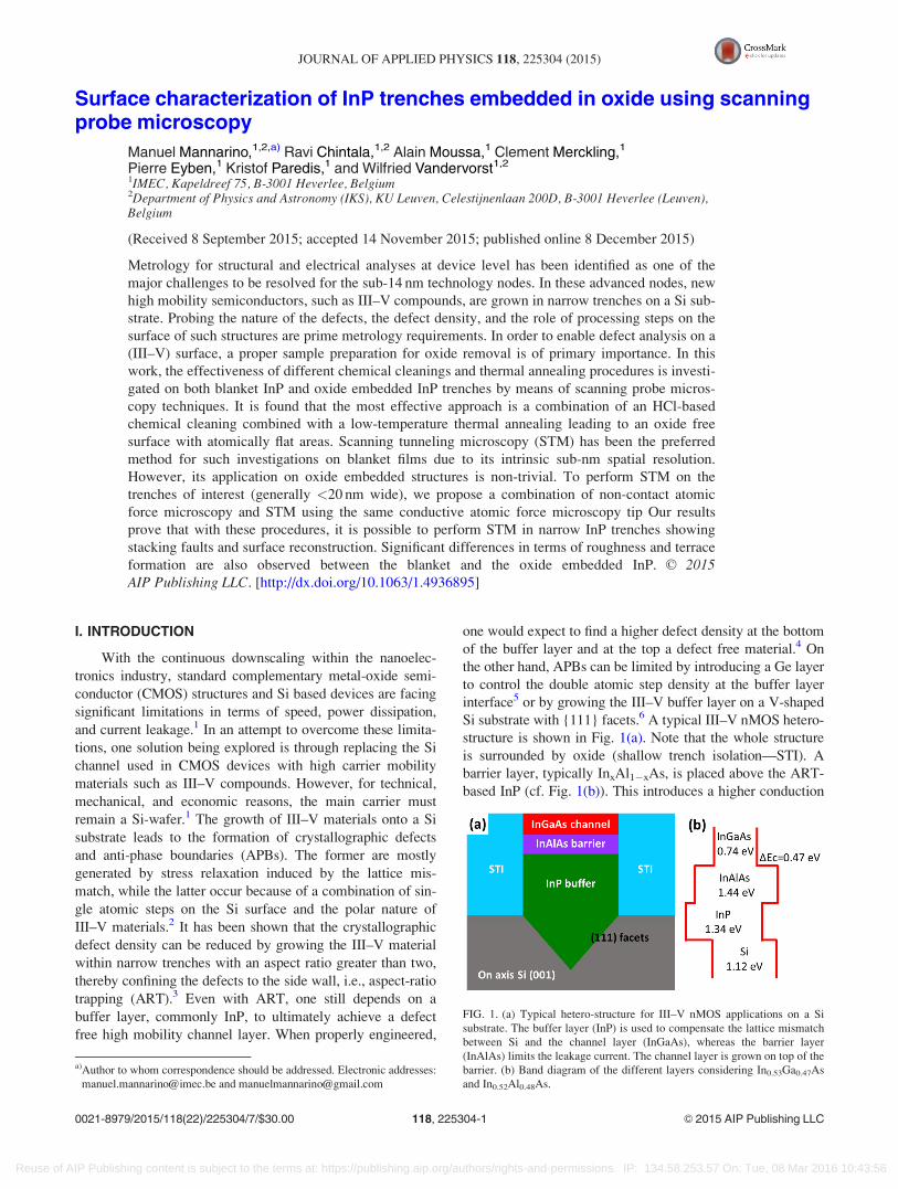
structure is shown in Fig. 1(a). Note that the whole structure
is surrounded by oxide (shallow trench isolation—STI). A
barrier layer, typically InxAl1�xAs, is placed above the ART-
based InP (cf. Fig. 1(b)). This introduces a higher conduction
FIG. 1. (a) Typical hetero-structure for III–V nMOS applications on a Si
substrate. The buffer layer (InP) is used to compensate the lattice mismatch
between Si and the channel layer (InGaAs), whereas the barrier layer
(InAlAs) limits the leakage current. The channel layer is grown on top of the
barrier. (b) Band diagram of the different layers considering In0.53Ga0.47As
and In0.52Al0.48As.
a)Author to whom correspondence should be addressed. Electronic addresses:
[email protected] and [email protected]
0021-8979/2015/118(22)/225304/7/$30.00 VC 2015 AIP Publishing LLC118, 225304-1
JOURNAL OF APPLIED PHYSICS 118, 225304 (2015)
Reuse of AIP Publishing content is subject to the terms at: https://publishing.aip.org/authors/rights-and-permissions. IP: 134.58.253.57 On: Tue, 08 Mar 2016 10:43:56

band offset between the high mobility channel (InGaAs in this
case) and the InP buffer layer, thereby reducing any leakage
current component present.7 Finally, on top of the barrier
layer a high mobility InxGa1�xAs channel is grown. The over-
all electrical properties of the channel are strongly influenced
by the quality of the underlying layers. Therefore, achieving
an InP buffer layer with an almost defect free surface is of pri-
mary importance. Besides, the identification and characteriza-
tion of the planar (stacking faults (SFs), twins, APBs) and
linear (dislocations) defects formed during the growth proc-
esses are fundamental to the material growth, device forma-
tion, and process optimization.
The metrology required for the structural and electrical
analysis at a device level today has been identified as one of
the major challenges to be resolved by the ITRS roadmap,8
especially for the next technology nodes. Hence, developing
the metrology to be able to probe the nature of the defects
and their electrical behavior within very confined volumes is
required. Among the scanning probe microscopy (SPM)
based techniques, scanning tunneling microscopy (STM) is
well known for its sub-nm spatial resolution for topographic
analysis and its ability to evaluate the electrical properties of
(semi-)conducting materials over a very localized area.9,10
Therefore, STM should in principle be suitable for the inves-
tigation of the crystalline properties and the presence of any
defects in (III–V) semiconductors. However, since STM uses
the tunneling current as a feedback signal to control the
height of the tip, only conductive surfaces can be probed.
This means that when STM has to be performed on a small
device surrounded by oxide, the tip needs to be positioned
very precisely above the narrow trench in order to avoid the
tip colliding with the oxide. In this work, we overcome the
STM-tip positioning by using a combination of non-contact
atomic force microscopy (nc-AFM) and STM in subsequent
scans. Despite the fact that the combination of nc-AFM and
STM with the same tip has already been demonstrated,11–14
in most of the existing literature the tip is scanned in constant
height mode such that tunneling current and shift of the reso-
nant frequency can be recorded at the same time. Only in
very few cases, nc-AFM and STM are performed in subse-
quent scans by using their respective feedback mecha-
nisms.15 An important point to note is that in all previously
reported works, the sample surfaces were almost atomically
flat. Contrary to this, our material grown in trenches includes
steps higher than 10–15 nm at the interface with the STI.
This makes the study of such a structure non-trivial preclud-
ing, for instance, the possibility to perform simultaneous nc-
AFM and STM measurements.
Another challenge arises from the fact that when dealing
with structures prepared on a 300 mm wafer in a standard
(industrial) CMOS processing line, structures have undergone
(surface roughening) processes like chemical mechanical pol-
ishing (CMP) and they are exposed to the (oxidizing) ambient.
As such, these surfaces differ significantly from in-situ grown
and characterized surfaces. To enable defect characterization at
an atomic scale by STM, oxide free and atomically flat surfaces
are fundamental requirements. The standard approaches for
(native) oxide removal typically involve a high temperature
anneal which, in the case of InP, leads to surface degradation
due to P desorption and In nucleation.16,17 Wet chemical clean-
ings for oxide removal are efficient but do not provide a proper
surface passivation18–21 and cannot prevent some III–V re-
oxidation during and after the rinsing bath. Finally, for sputter-
ing approaches it is still not clear whether the surface is
affected by implantation and/or roughening.22,23
The work presented herein focuses on the analysis of
epitaxial InP grown on a InP substrate (2-in. wafer) and InP
grown on V-shaped Si trenches.24 We have investigated the
effectiveness of thermal annealing and chemical cleanings
(HF and HCl) for native oxide removal and terrace formation
on the blanket samples. Furthermore, we have subsequently
explored the combination of nc-AFM and STM, using the
same conductive atomic force microscopy (AFM) tip, to suc-
cessfully analyze the InP embedded in an oxide matrix.
II. EXPERIMENTAL
The 2-in. InP (100) blanket wafers adopted for this
work were doped with zinc to a carrier concentration of
1� 1018 cm�3 (wafers provided by AXT Inc.). Patterned
samples were produced in house using our standard process
as described in more detail within Ref. 24. They are based
on the creation of narrow trenches with oxide isolation
(STI), epitaxial growth on V-shaped Si trenches, and a final
CMP step for the removal of any overgrown material. The
samples were subsequently treated ex-situ and under dark
conditions (to avoid photo-stimulated etching) in either a HF
2% or 0.25 M H2O2/1 M HCl and 2 M HCl solutions. After
the chemical treatment, the samples were rinsed in deionized
water and exposed to air for about 3–5 min. Once inside the
load lock of the UHV chamber, a pressure of 3� 10�7 Torr
was reached in �5 min. To desorb any hydrocarbons on the
sample surface, the load lock was baked (160 �C for 6 h)
with the sample inside. After transferring the sample into the
UHV-SPM chamber, a further thermal anneal was performed
using radiative heating from a W filament underneath the
sample. In this case, the heating rate was initially 5 �C/min
but was lowered to 4 �C/min and 3 �C/min reaching 220 �Cand 280 �C, respectively. The cooling process followed
the reverse trend. STM and nc-AFM were performed in
the UHV system equipped with a scanning electron micro-
scope (RHK 3500 HT). All the measurements were carried
out at room temperature under a vacuum of �5� 10�10 Torr.
Commercial Pt/Ir STM tips and Pt/Ir coated AFM tips with a
cantilever spring constant of 42 N/m (nominal value) were
used for the measurements. All the data were analyzed with
the WSxM software.25
III. RESULTS AND DISCUSSION
A. Preparation of an oxide free, undamaged InPsurface
In order to analyze the InP surface at atomic level, the
native oxide has to be removed and the surface should
ideally exhibit atomically flat regions. Although such an ox-
ide can be removed by a simple thermal anneal, phosphorus
evaporation and indium nucleation are phenomena that have
been previously observed when InP is raised to a temperature
225304-2 Mannarino et al. J. Appl. Phys. 118, 225304 (2015)
Reuse of AIP Publishing content is subject to the terms at: https://publishing.aip.org/authors/rights-and-permissions. IP: 134.58.253.57 On: Tue, 08 Mar 2016 10:43:56
suitable for the oxide removal. In many published works,
this problem is tackled by annealing the sample under P226,27
or by Arþ sputtering in combination with a thermal anneal-
ing step.28,29 As these approaches are not applicable here
because they would degrade the material integrity, to avoid
topographic and/or compositional changes (e.g., implanta-
tion),22,23 we only made use of controlled thermal annealing
within the UHV chamber. During our experiments, we did
observe InP decomposition when we reached �400 �C.
Figure S1 of the supplementary material30 shows an optical
image of a sample annealed at 400 �C. Different morphologi-
cal shapes of the indium metallic clusters are seen to co-exist
on the same sample, i.e., h011i oriented, merged, and ran-
domly distributed. As the change from one shape to another
requires only a few tens of �C,16 their co-existence is not sur-
prising because it is believed to be driven by their formation
kinetics. For example, by keeping a constant temperature of
375 �C, the surface starts to degrade after �15 min, whereas
at �400 �C, the degradation is immediate. By optimizing the
annealing temperature and the heating rate, it is therefore
possible to remove the oxide layer and to limit, up to a cer-
tain extent, the surface degradation. As one might expect, at
375 �C it is much easier to limit the morphological changes
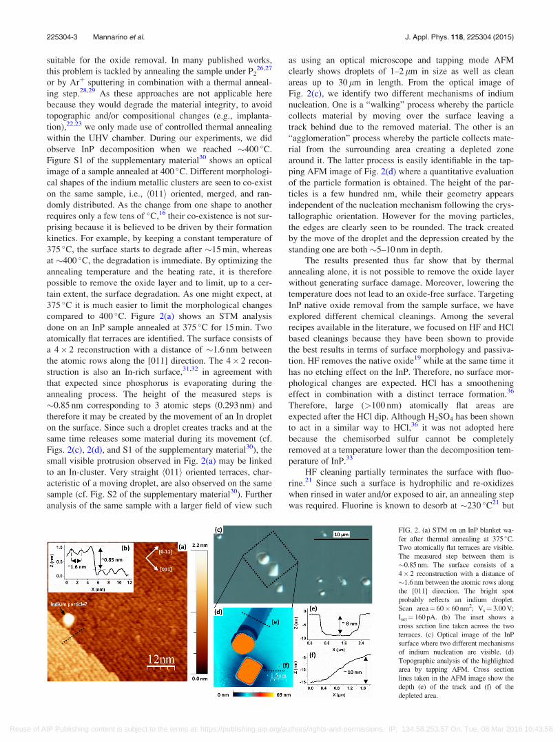
compared to 400 �C. Figure 2(a) shows an STM analysis
done on an InP sample annealed at 375 �C for 15 min. Two
atomically flat terraces are identified. The surface consists of
a 4� 2 reconstruction with a distance of �1.6 nm between
the atomic rows along the [011] direction. The 4� 2 recon-
struction is also an In-rich surface,31,32 in agreement with
that expected since phosphorus is evaporating during the
annealing process. The height of the measured steps is
�0.85 nm corresponding to 3 atomic steps (0.293 nm) and
therefore it may be created by the movement of an In droplet
on the surface. Since such a droplet creates tracks and at the
same time releases some material during its movement (cf.
Figs. 2(c), 2(d), and S1 of the supplementary material30), the
small visible protrusion observed in Fig. 2(a) may be linked
to an In-cluster. Very straight h011i oriented terraces, char-
acteristic of a moving droplet, are also observed on the same
sample (cf. Fig. S2 of the supplementary material30). Further
analysis of the same sample with a larger field of view such
as using an optical microscope and tapping mode AFM
clearly shows droplets of 1–2 lm in size as well as clean
areas up to 30 lm in length. From the optical image of
Fig. 2(c), we identify two different mechanisms of indium
nucleation. One is a “walking” process whereby the particle
collects material by moving over the surface leaving a
track behind due to the removed material. The other is an
“agglomeration” process whereby the particle collects mate-
rial from the surrounding area creating a depleted zone
around it. The latter process is easily identifiable in the tap-
ping AFM image of Fig. 2(d) where a quantitative evaluation
of the particle formation is obtained. The height of the par-
ticles is a few hundred nm, while their geometry appears
independent of the nucleation mechanism following the crys-
tallographic orientation. However for the moving particles,
the edges are clearly seen to be rounded. The track created
by the move of the droplet and the depression created by the
standing one are both �5–10 nm in depth.
The results presented thus far show that by thermal
annealing alone, it is not possible to remove the oxide layer
without generating surface damage. Moreover, lowering the
temperature does not lead to an oxide-free surface. Targeting
InP native oxide removal from the sample surface, we have
explored different chemical cleanings. Among the several
recipes available in the literature, we focused on HF and HCl
based cleanings because they have been shown to provide
the best results in terms of surface morphology and passiva-
tion. HF removes the native oxide19 while at the same time it
has no etching effect on the InP. Therefore, no surface mor-
phological changes are expected. HCl has a smoothening
effect in combination with a distinct terrace formation.36
Therefore, large (>100 nm) atomically flat areas are
expected after the HCl dip. Although H2SO4 has been shown
to act in a similar way to HCl,36 it was not adopted here
because the chemisorbed sulfur cannot be completely
removed at a temperature lower than the decomposition tem-
perature of InP.33
HF cleaning partially terminates the surface with fluo-
rine.21 Since such a surface is hydrophilic and re-oxidizes
when rinsed in water and/or exposed to air, an annealing step
was required. Fluorine is known to desorb at �230 �C21 but
FIG. 2. (a) STM on an InP blanket wa-
fer after thermal annealing at 375 �C.
Two atomically flat terraces are visible.
The measured step between them is
�0.85 nm. The surface consists of a
4� 2 reconstruction with a distance of
�1.6 nm between the atomic rows along
the [011] direction. The bright spot
probably reflects an indium droplet.
Scan area¼ 60� 60 nm2; Vs¼ 3.00 V;
Iset¼ 160 pA. (b) The inset shows a
cross section line taken across the two
terraces. (c) Optical image of the InP
surface where two different mechanisms
of indium nucleation are visible. (d)
Topographic analysis of the highlighted
area by tapping AFM. Cross section
lines taken in the AFM image show the
depth (e) of the track and (f) of the
depleted area.
225304-3 Mannarino et al. J. Appl. Phys. 118, 225304 (2015)
Reuse of AIP Publishing content is subject to the terms at: https://publishing.aip.org/authors/rights-and-permissions. IP: 134.58.253.57 On: Tue, 08 Mar 2016 10:43:56

to remove the oxide a higher temperature is required.
Therefore, after a dip in a 2% aqueous HF solution for
1.5 min, the sample was annealed at 340 �C within the UHV
chamber. An STM image of the sample surface is shown in
Fig. 3. Although we can evaluate the morphological quality
of the surface, it was not possible to identify atomic-scale
crystallographic defects because no distinguishable atomi-
cally flat terraces are observed. Additionally, no surface
reconstruction can be observed even in small scan areas. An
InP (001) oxide-free surface implies the presence of dangling
bonds and a rearrangement of the atoms on the surface in
order to minimize their surface energy. However, a regular
and ordered surface, as observed for instance in Fig. 2(a), is
only possible within atomically flat areas. It should be noted
that the investigated sample did undergo a CMP step which
gives rise to surface roughness which cannot be recovered by
our current HF cleaning and annealing processes. A higher
temperature thermal anneal could provide enough energy to
induce an atomic rearrangement of the top surface. However,
this would probably lead, as in the case of the simple thermal
annealing, to a degradation of the surface.
The second recipe investigated in this work is based on
H2O2 and HCl. It consists of an etching step and an oxide re-
moval step.34,35 In particular, for the etching we used 0.25 M
H2O2/1 M HCl for 5 min, while the oxide removal was car-
ried out using 2 M HCl for 5 min. During the etching pro-
cess, a few nanometers of the top surface are removed by an
oxide formation/oxide dissolution process.34 In this work,
we are mostly interested in planar and linear defects arising
from the lower region of the buffer layer which form during
growth. Therefore, even if a few nanometers are removed
from the top surface, the defects and their distribution are
not affected. Through the second step, the HCl dip, the oxide
layer is removed producing a partially passivated sur-
face.18,21 This cleaning process allows to achieve very
smooth surfaces with distinct atomically flat terraces.34–36
Figure 4(a) shows the STM analysis of the InP surface after
the cleaning and the insertion into the UHV chamber.
Elongated terraces up to �100 nm in length are observed. As
atoms are less stable at the step edges, they are removed dur-
ing the HCl dip. Therefore, atomically flat terraces are gener-
ated and enlarged. The step height between the terraces is
�0.3 nm (single atomic step). However, when reducing the
scan area and focusing on one single atomic flat terrace, the
images became significantly noisy and blurry (not shown).
This is due to the partial surface passivation combined with a
thin oxide layer formed during the sample mounting.18,21 In
order to obtain a completely clean surface, this chemical
treatment was combined with a thermal annealing inside the
UHV chamber. After annealing at 300 �C, an oxide-free and
reconstructed (4� 2) InP surface was obtained, as shown in
Fig. 4(c). The required temperature was �70 �C lower than
FIG. 3. STM on InP after HF dip and thermal annealing at 340 �C. No
surface reconstruction nor atomic terraces are visible. Scan area¼ 300
� 300 nm2, Vs¼ 3.00 V, Iset¼ 100 pA.
FIG. 4. (a) STM on InP (100) blanket
after an HCl-based wet cleaning. Atomic
terraces in the order of 100 nm long are
generated during the HCl dip. Scan
area¼ 400� 400 nm2, Vs¼ 2.80 V, Iset
¼ 150 pA. (b) A cross section line taken
across the terraces shows a step height
of �0.3 nm. (c) STM after wet cleaning
and thermal annealing at 300 �C.
Terrace borders show a different mor-
phology compared to the non-annealed
sample. Scan area¼ 400� 400 nm2, Vs
¼ 2.80 V, Iset¼ 150 pA. In the inset a
smaller scan area shows a 4� 2 recon-
structed surface. (d) A cross section line
taken across two terraces in the inset of
(c), an atomic step and the reconstruc-
tion profile are identifiable.
225304-4 Mannarino et al. J. Appl. Phys. 118, 225304 (2015)
Reuse of AIP Publishing content is subject to the terms at: https://publishing.aip.org/authors/rights-and-permissions. IP: 134.58.253.57 On: Tue, 08 Mar 2016 10:43:56

that without chemical treatment which has the added advant-
age of limiting the surface from degrading. Moreover, con-
sidering that all the steps of the InP growth are generally
done at temperatures higher than 400 �C,24 it minimizes any
effect on the original crystallographic defect distribution.
The lower thermal budget to achieve oxide evaporation is
because the regrown oxide is only 0.2–0.3 nm as shown by
van Dorp et al.,35 which is substantially thinner than the
native oxide. Another feature of interest after thermal
annealing is the shape of the edges of the terraces. Compared
to the non-annealed sample, where the borders are straight
over long distances, here they appear jagged while the ter-
race size is smaller. This can be explained because atoms at
the step edges are chemically less stable; thus, they evapo-
rate and/or move more easily due to the energy acquired
during the thermal treatment. This process therefore reduces
the terrace size and induces a more random orientation.
However, the most important result of Fig. 4(c) is that
the surface quality achieved is suitable for STM
characterization.
B. STM measurements in narrow trenches embeddedin oxides
To targeting high quality material for the device fabrica-
tion, the III–Vs are grown in trenches with widths below
20 nm. Classical measurement techniques must therefore be
modified to perform a proper characterization when dealing
with such small dimensions. When dealing with relatively
large trenches (>300–500 nm), the STM tip can readily be
positioned above the trench by guiding it with a scanning
electron microscopy (SEM) image generated simultaneously.
This allows to land the STM tip exactly above the InP.
However, for smaller dimensions, the resolution limits of the
SEM and the physical dimensions of the STM tip require an
alternative approach. The approach we have adopted is based
on the combination of nc-AFM and STM while using the
same conductive AFM probe. The tip is first utilized in nc-
AFM mode to locate the narrow trench of interest and, once
in place, its operation mode is switched to STM (cf. Fig. S3
of the supplementary material30). In principle, this approach
should not have any limitation with respect to the downscal-
ing of the trench. A shifted probing point could only be
linked to the different tip-sample interaction area of the two
modes. Considering a typical tip radius <30 nm, a shift
larger than a few nanometers seems unlikely. One of the key
challenges in this approach is to match the tip and cantilever
requirements for the nc-AFM, which uses the cantilever as a
force sensor in oscillation mode, to that of the STM which
relies on the tunneling current to control the tip height oper-
ating in non-oscillation mode. First and foremost the tip
must be sharp and have a metallic behavior to reach atomic
resolution and enable extraction of electrical information
such as I–V spectroscopy. Moreover, a certain cantilever
stiffness to avoid snap-in due to the electrostatic forces and
low noise in the z-direction is also a requirement of this
approach. According to the simulations done by Ozcan and
Sitti,37 an AFM-cantilever must have a minimum spring con-
stant of 15 N/m for use in STM-mode, although this is just
an indicative value since tip radius/shape and bias affect
the electrostatic forces. We have screened various tips and
the best results are obtained using relatively stiff Pt/Ir coated
tips with a nominal spring constant of 42 N/m. Effective
stiffness was evaluated by thermal tune38 and was found to
be 29 6 3 N/m. Figure 5 shows an STM analysis performed
on a blanket InP sample using this tip and exhibiting atomic
corrugation.
Based on these results we tested the proposed localiza-
tion approach on a 500 nm wide InP trench. Figure 6(a)
shows a topography image using the nc-AFM mode before
switching to STM. As the sample was treated with HF, the
InP-trench material is easily identified. Since the HF not
only attacks the native oxide on the InP but also etches the
surrounding oxide, the trench emerges as a small hillock
with respect to the STI. The STI is �12 nm lower than InP.
Comparing the original surface topography (not shown),
where some material removal (�13 nm) in the trench region
is observed after the CMP-step, the vertical etch of the STI
was determined to be �25 nm. The protrusions at the edges
of the InP originate from the CMP process which has a lower
removal rate at the interface with the STI. Once the trench is
centered within the scan area, it is possible to switch to the
FIG. 5. Surface reconstruction imaged using STM with a Pt/Ir coated AFM
tip 42 N/m on an InP(100) blanket sample. Scan area¼ 80 � 60 nm2,
Vs¼�2.8 V, Iset¼�100 pA.
FIG. 6. (a) nc-AFM on a patterned InP sample after HF dip and thermal
annealing at 370 �C. The well-shaped InP with the (110) sidewalls is visible.
The STI is �12 nm lower than the InP. Scan area¼ 1� 1 lm2, Df¼�2 Hz.
(b) STM on top of the InP by using the same AFM tip. The surface appears
rough but with small atomically flat areas. Locally the small terraces show
a 4� 2 surface reconstruction. Scan area¼ 60� 30 nm2, Vs¼�3.00 V,
Iset¼�130 pA, z-scale¼ 1.4 nm. (c) A cross section line taken in the high-
lighted area shows a distance of 1.6 nm between the atomic rows.
225304-5 Mannarino et al. J. Appl. Phys. 118, 225304 (2015)
Reuse of AIP Publishing content is subject to the terms at: https://publishing.aip.org/authors/rights-and-permissions. IP: 134.58.253.57 On: Tue, 08 Mar 2016 10:43:56
STM-mode. Figure 6(b) shows the STM image of the
top InP surface. Compared to the blanket sample, a rougher
surface with smaller atomically flat areas is visible.
Nevertheless, the terraces are still observed and have a 4� 2
surface reconstruction. The surface reconstruction implies
that the oxide layer is completely removed, while the sur-
rounding protrusions can be linked to an initial degradation
process activated by the thermal annealing. In this specific
case, the sample was annealed at 370 �C for 10 min. The
proposed localization approach has been used on trench
width down to 200 nm (see Fig. S4 of the supplementary ma-
terial30) and no fundamental limitations have as yet been
encountered.
C. Oxide removal and STM analysis of InP grownin trenches
The HCl-based cleaning when combined with a low
(�300 �C) thermal annealing leads to, certainly on a blanket
InP sample, a surface suitable for STM analysis and defect
characterization. Targeting similar surface properties on InP
grown in trenches, we have used the same optimized sample
preparation procedure developed for blanket samples. A large
scale analysis shows a morphological degradation of the
{110} sidewalls and a considerable anisotropic etching at the
defect location (cf. Fig. S5 of the supplementary material30).
According to van Dorp et al., an etch rate of 1.3 nm/min
is expected for a blanket {110} surface using 2 M HCl.35
However, the evaluated etch rate for our patterned sample is
found to be �10 times faster. The reason for such a discrep-
ancy is at present unclear but could be linked to the higher
defect density and to Fermi level pinning on the electrochem-
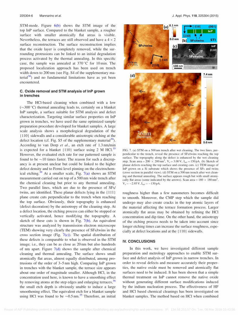
ical etching.39 At a smaller scale, Fig. 7(a) shows an STM
measurement carried out on top of a 500 nm wide trench after
the chemical cleaning but prior to any thermal annealing.
Two parallel lines, which are due to the presence of SFs/
twins, are identified. These planar defects lying in the {111}
plane create cuts perpendicular to the trench when reaching
the top surface. Obviously, their topography is enhanced
(defect decoration) by the anisotropy of the cleaning step. At
a defect location, the etching process can either be stopped or
vertically activated, hence modifying the topography. A
sketch of these cuts is shown in Fig. 7(b). An equivalent
structure was analyzed by transmission electron microscope
(TEM) showing very clearly the presence of SFs/twins in the
cross section image (Fig. 7(c)). The spatial distribution of
these defects is comparable to what is observed in the STM
image; i.e., they can be as close as 20 nm but also hundreds
of nm apart. Figure 7(d) shows the sample after chemical
cleaning and thermal annealing. The surface shows small
atomically flat areas, almost equally distributed, among pro-
trusions of the order of 3–5 nm high. Comparing InP grown
in trenches with the blanket sample, the terrace size appears
about one order of magnitude smaller. Although HCl, in the
concentration used here, is known to have a smoothing effect
by removing atoms at the step edges and enlarging terraces,36
the small etch depth is obviously unable to induce a large
smoothening effect. The equivalent etch for a blanket sample
using HCl was found to be �0.5 nm.35 Therefore, an initial
roughness higher than a few nanometers becomes difficult
to smooth. Moreover, the CMP step which the sample did
undergo may also create cracks in the top atomic layers of
the material affecting the terrace formation process. Larger
atomically flat areas may be obtained by refining the HCl
concentration and dip time. On the other hand, the anisotropy
of the etching process needs to be taken into account since
longer etching times can increase the surface roughness, espe-
cially at defect locations and at the {110} sidewalls.
IV. CONCLUSIONS
In this work, we have investigated different sample
preparation and metrology approaches to enable STM sur-
face and defect analysis of InP grown in narrow trenches. In
order to reveal defects and measure accurately their proper-
ties, the native oxide must be removed and atomically flat
surfaces need to be induced. It has been shown that a simple
thermal treatment on InP cannot remove the native oxide
without generating different surface modifications induced
by the indium nucleation process. The effectiveness of HF
and HCl based chemical cleanings has been investigated on
blanket samples. The method based on HCl when combined
FIG. 7. (a) STM on a 500 nm trench after wet cleaning. The two lines, per-
pendicular to the trench, reveal the presence of SFs/twins reaching the top
surface. The topography along the defect is enhanced by the wet cleaning
step. Scan area¼ 200 � 200 nm2, Vs¼ 3.00 V, Iset¼ 150 pA. (b) Sketch of
planar defects reaching the top surface and creating cuts. (c) TEM image of
InP grown on a Si substrate which shows the presence of SFs and twins
(cross section in parallel view). (d) STM on a 500 nm trench after wet clean-
ing and thermal annealing. The surface appears rough but with small atomi-
cally flat areas (some indicated by the arrows). Scan area¼ 180 � 180 nm2,
Vs¼�2.95 V, Iset¼�130 pA.
225304-6 Mannarino et al. J. Appl. Phys. 118, 225304 (2015)
Reuse of AIP Publishing content is subject to the terms at: https://publishing.aip.org/authors/rights-and-permissions. IP: 134.58.253.57 On: Tue, 08 Mar 2016 10:43:56

with a low-temperature thermal annealing produces a better
surface quality which is suitable for STM analysis and defect
characterization. It allows to remove the native oxide layer,
to avoid surface degradation, and to generate atomically flat
terraces. Oxide-free InP surfaces were confirmed by STM
analysis showing a 4� 2 surface reconstruction.
For patterned samples, it has been identified that a higher
defect density, roughness due to process steps (e.g., CMP),
and the presence of different surface planes have a strong
impact in the terrace formation process. Moreover, we have
successfully performed STM analysis on InP trenches embed-
ded in an oxide matrix using a combination of nc-AFM and
STM. The chosen approach uses the same conductive AFM
tip to perform nc-AFM to localize the trench and then to per-
form STM in the selected trench area. A proper selection of
the AFM probe allows to obtain sub-nm resolution in STM
mode. With this combined approach, trenches were easily
identified and an STM surface analysis could be performed.
Observation of surface reconstruction and stacking faults/
twins defects reaching the top surface has been shown.
ACKNOWLEDGMENTS
The authors would like to thank the MCA-SA Team for
the TEM analysis and Dr. Richard Morris for his valuable
comments and suggestions through the writing of this
manuscript.
1J. A. del Alamo, Nature 479, 317 (2011).2D. Cohen and C. B. Carter, J. Microsc. 208, 84 (2002).3E. A. Fitzgerald and N. Chand, J. Electron. Mater. 20, 839 (1991).4C. Merckling, N. Waldron, S. Jiang, W. Guo, O. Richard, B. Douhard, A.
Moussa, D. Vanhaeren, H. Bender, N. Collaert, M. Heyns, A. Thean, M.
Caymax, and W. Vandervorst, J. Appl. Phys. 114, 033708 (2013).5G. Wang, M. R. Leys, R. Loo, O. Richard, and H. Bender, Appl. Phys.
Lett. 97, 121913 (2010).6M. Paladugu, C. Merckling, R. Loo, O. Richard, H. Bender, J. Dekoster,
W. Vandervorst, M. Caymax, and M. Heyns, Cryst. Growth Des. 12, 4696
(2012).7H. Zhao, Y. Chen, J. H. Yum, Y. Wang, F. Zhou, F. Xue, and J. C. Lee,
Appl. Phys. Lett. 96, 102101 (2010).8See http://www.itrs.net/ITRS%201999-2014%20Mtgs,%20Presentations%
20&%20Links/2013ITRS/2013Chapters/2013Metrology_Summary.pdf for
International Technology Roadmap for Semiconductors, Metrology
Summary, Accessed 8 September 2015, 2013.9R. J. Hamers, R. M. Tromp, and J. E. Demuth, Phys. Rev. Lett. 56, 1972
(1986).10R. M. Feenstra, Surf. Sci. 299/300, 965 (1994).11F. J. Giessibl and B. M. Trafas, Rev. Sci. Instrum. 65, 1923 (1994).
12Z. Majzik, M. R. Tchalala, M. �Svec, P. Hapala, H. Enriquez, A. Kara, A. J.
Mayne, G. Dujardin, P. Jel�ınek, and H. Oughaddou, J. Phys. Condens.
Matter 25, 225301 (2013).13A. J. Weymouth, T. Wutscher, J. Welker, T. Hofmann, and F. J. Giessibl,
Phys. Rev. Lett. 106, 226801 (2011).14D. Sawada, Y. Sugimoto, K. Morita, M. Abe, and S. Morita, Appl. Phys.
Lett. 94, 173117 (2009).15M. Iwatsuki, K. Suzuki, S. Kitamura, and M. Kersker, Microsc. Microanal.
5, 208 (1999).16F. Riesz, L. Dobos, and J. Karanyi, J. Vac. Sci. Technol. B 16, 2672
(1998).17C. R. Bayliss and D. L. Kirk, J. Phys. D 9, 233 (1976).18D. Kikuchi, Y. Matsui, and S. Adachi, J. Electrochem. Soc. 147, 1973
(2000).19D. Kikuchi and S. Adachi, Mater. Sci. Eng. B 76, 133 (2000).20T. Chass, H. Peisert, P. Streubel, and R. Szargan, Surf. Sci. 331/333, 434
(1995).21Y. Sun, Z. Liu, F. Machuca, P. Pianetta, and W. E. Spicer, J. Appl. Phys.
97, 124902 (2005).22E. Taglauer, Appl. Phys. A 51, 238 (1990).23F. Stietz, T. Allinger, V. Polyakov, J. Woll, A. Goldmann, W. Erfurth,
G. J. Lapeyre, and J. A. Schaefer, Appl. Surf. Sci. 104/105, 169 (1996).24C. Merckling, N. Waldron, S. Jiang, W. Guo, N. Collaert, M. Caymax, E.
Vancoille, K. Barla, A. Thean, M. Heyns, and W. Vandervorst, J. Appl.
Phys. 115, 023710 (2014).25I. Horcas, R. Fernandez, J. M. Gomez-Rodriguez, J. Colchero, J. Gomez-
Herrero, and A. M. Baro, Rev. Sci. Instrum. 78, 013705 (2007).26Q. Guo, M. E. Pemble, and E. M. Williams, Surf. Sci. 468, 92 (2000).27Y. Ishikawa, T. Fukui, and H. Hasegawa, J. Vac. Sci. Technol. B 15, 1163
(1997).28S. Ohkouchi and I. Tanaka, App. Phys. Lett. 59, 1588 (1991).29O. Crisan, Trans. F: Nanotechnol. 17, 154 (2010).30See supplementary material at http://dx.doi.org/10.1063/1.4936895 for InP
surface morphology after a thermal anneal at 400 �C, h110i oriented terra-
ces generated by a moving In cluster, methodology to enable STM analysis
of trenches embedded in oxides, STM analysis of a 200 nm wide trench,
and HCl impact on InP grown in trenches.31M. Shimomura, N. Sanada, Y. Fukuda, and P. J. Moller, Surf. Sci. 359,
L451 (1996).32M. M. Sung, C. Kim, H. Bu, D. S. Karpuzov, and J. W. Rabalais, Surf.
Sci. 322, 116 (1995).33V. Chab, L. Pekarek, I. Ulrych, J. Suchy, K. C. Prince, M. Peloi, M.
Evans, C. Comicioli, M. Zacchigna, and C. Crotti, Surf. Sci. 377–379, 261
(1997).34D. Cuypers, S. De Gendt, S. Arnauts, K. Paulussen, and D. H. van Dorp,
ECS J. Solid State Sci. Technol. 2, P185 (2013).35D. H. van Dorp, D. Cuypers, S. Arnauts, A. Moussa, L. Rodriguez, and S.
De Gendt, ECS J. Solid State Sci. Technol. 2, P190 (2013).36D. Cuypers, D. H. van Dorp, M. Tallarida, S. Brizzi, T. Conard, L. N. J.
Rodriguez, M. Mees, S. Arnauts, D. Schmeisser, C. Adelmann, and S. De
Gendt, ECS J. Solid State Sci. Technol. 3, N3016 (2014).37O. Ozcan and M. Sitti, Micro Nano Lett. 7, 329 (2012).38J. L. Hutter and J. Bechhoefer, Rev. Sci. Instrum. 64, 1868 (1993).39A. J. Bard, A. B. Bocarsly, F. F. Fan, E. G. Walton, and M. S. Wrighton,
J. Am. Chem. Soc. 102, 3671 (1980).
225304-7 Mannarino et al. J. Appl. Phys. 118, 225304 (2015)
Reuse of AIP Publishing content is subject to the terms at: https://publishing.aip.org/authors/rights-and-permissions. IP: 134.58.253.57 On: Tue, 08 Mar 2016 10:43:56