sublimation of gete nanowires and evidence of its size effect studied by in situ tem
TRANSCRIPT

Sublimation of GeTe Nanowires and Evidence of Its SizeEffect Studied by in Situ TEM
Joanne W. L. Yim,†,‡ Bin Xiang,†,‡ and Junqiao Wu*,†,‡
Department of Materials Science and Engineering, UniVersity of California, Berkeley,Berkeley, California 94720, and Materials Sciences DiVision, Lawrence Berkeley National
Laboratory, Berkeley, California 94720
Received July 13, 2009; E-mail: [email protected]
Abstract: We report sublimation of crystalline GeTe nanowires at elevated temperatures in vacuum imagedby in situ transmission electron microscopy. The GeTe nanowires exhibit significant melting point suppressionin the presence of Au contamination. A nanosized effusion cell is formed by coating the GeTe core with aSiO2 shell, where the core can be evaporated or sublimated from the open end of the shell at hightemperatures. By measuring the speed of the moving interface between the condensed and vapor phases,we determined the vaporization coefficient of these nanowires to be greater than or equal to ∼10-3 overa wide range of temperatures. At the final stage of the nanowire vaporization, the material loss occurs ata higher rate, which is evidence of a higher vaporization coefficient for nanosized GeTe. This in situ techniqueoffers a quantitative method of investigating phase transition dynamics and kinetics of nanomaterials, animportant topic for designing nanoscale devices to be operated at high temperatures such as phase changememory.
Introduction
Phase-change memory has emerged as a strong contender forreplacing flash memory for nonvolatile memory technology.Phase-change material (PCM), commonly chalcogenides andmost popularly Ge2Sb2Te5 (GST), exhibiting an amorphous-crystalline transition under an applied electrical or opticalimpulse, can be probed for the existing bit state using eitherreflectivity or resistivity.1 The change in optical reflectivity isexploited in rewritable CD and DVD technology. Electricallyinterrogated PCM devices sandwich the PCM between anelectrode and a resistive heating element. To drive the systemto crystallize or amorphize, a large current pulse is applied tolocally heat the PCM. Devices in excess of 8MB have beenassembled with excellent data retention and cycle life;2 however,upon repeated cycling memory elements ultimately fail due tophase separation and loss of electrical contact integrity withelectrodes.3 While the active PCM is routinely encapsulated,the intense local heating required for switching introducesthermal stress which can damage the encapsulant and allow thePCM to evaporate.4 To prevent failure and optimize the designof high density data storage, it is important to understand thedynamic transition behavior of PCM from a condensed to vaporphase at the nanoscale.
Single crystalline nanowires of many PCMs have been grown,including GeTe,5-7 GST,8 Sb2Te3,
5 and In2Se3.9 High density
memory arrays constructed from GST nanowires have beenshown to withstand >105 write/rewrite cycles.8 Reducing theactive PCM volume can increase the crystallization speed andlower the power consumption.10 In addition, nanowires presenta convenient test-bed for investigating nanoscale phenomena,especially for in situ techniques. In situ transmission electronmicroscopy (TEM) heating experiments on metal nanoparticleshave identified surface melting and particle coalescence attemperatures much lower than in the bulk.11,12 Previous in situTEM heating experiments on encapsulated Ge nanowires haveshown a significant depression of the melting point correlatedwith nanowire diameter.13 Similarly, for GeTe nanowireswithout encapsulation, the PCM was observed to melt andsubsequently evaporate at temperatures lower than the bulkmelting point.14 With regard to device failure analysis, thedevelopment of a void in the active material volume during in
† University of California.‡ Lawrence Berkeley National Laboratory.
(1) Lacaita, A. L.; Wouters, D. J. Phys. Status Solidi A 2008, 205 (10),2281–2297.
(2) Pirovano, A.; Redaelli, A.; Pellizzer, F.; Ottogalli, F.; Tosi, M.; Ielmini,D.; Lacaita, A. L.; Bez, R. IEEE Trans. DeVice Mater. Reliab. 2004,4 (3), 422–427.
(3) Nam, S.-W.; Kim, C.; Kwon, M.-H.; Lee, H.-S.; Wi, J.-S.; Lee, D.;Lee, T.-Y.; Khang, Y.; Kim, K.-B. Appl. Phys. Lett. 2008, 92 (11),111913–3.
(4) Yin, Y.; Miyachi, A.; Niida, D.; Sone, H.; Hosaka, S. Jpn. J. Appl.Phys., Part 2 2006, 45 (28), L726–L726.
(5) Meister, S.; Peng, H.; McIlwrath, K.; Jarausch, K.; Zhang, X. F.; Cui,Y. Nano Lett. 2006, 6 (7), 1514–1517.
(6) Yu, D.; Wu, J.; Gu, Q.; Park, H. J. Am. Chem. Soc. 2006, 128 (25),8148–8149.
(7) Jennings, A. T.; Jung, Y.; Engel, J.; Agarwal, R J. Phys. Chem. C2009, 113 (17), 6898–6901.
(8) Lee, S.-H.; Jung, Y.; Agarwal, R. Nat. Nanotechnol. 2007, 2 (10),626–630.
(9) Sun, X.; Yu, B.; Ng, G.; Nguyen, T. D.; Meyyappan, M. Appl. Phys.Lett. 2006, 89 (23), 233121–3.
(10) Milliron, D. J.; Raoux, S.; Shelby, R. M.; Jordan-Sweet, J. Nat. Mater.2007, 6 (5), 352–356.
(11) Mohamed, M. B.; Wang, Z. L.; El-Sayed, M. A. J. Phys. Chem. A1999, 103 (49), 10255–10259.
(12) Wang, Z. L.; Petroski, J. M.; Green, T. C.; El-Sayed, M. A J. Phys.Chem. B 1998, 102 (32), 6145–6151.
(13) Wu, Y.; Yang, P. AdV. Mater. 2001, 13 (7), 520–523.(14) Sun, X.; Yu, B.; Ng, G.; Meyyappan, M. J. Phys. Chem. C 2007, 111
(6), 2421–2425.
Published on Web 09/15/2009
10.1021/ja905808d CCC: $40.75 2009 American Chemical Society14526 9 J. AM. CHEM. SOC. 2009, 131, 14526–14530
situ electrical biasing highlights the importance of understandingand preventing PCM loss during cycling.15 Here we report ona method utilizing in situ microscopy to evaluate the speed ofevaporation and sublimation of nanomaterials.
Experimental Section
The GeTe nanowires were grown using the standard Au-catalyzedvapor-liquid-solid (VLS) method.6 GeTe source powder (AlfaAesar 99.999%) sublimated at the center of a 1 in. tube furnacewas transported by 120 sccm Ar downstream to a SiO2 substratecovered with 40 nm diameter Au colloids (Ted Pella). A vacuumpump was run continuously to set the furnace pressure at ∼10 Torr.The source was held at 400 °C and the receiving substrates at ∼350°C for 5 h and then allowed to cool naturally. The nanowires weremanually transferred to a molybdenum TEM grid with a laceycarbon film, and the entire grid was coated with an amorphous SiO2
shell using low temperature plasma enhanced chemical vapordeposition (PECVD). The SiO2 coating was typically nonconformalat the nanowire ends; this is due possibly to the sharp edges ofnanowire there, leading to pores or openings in the SiO2 at theends. The SiO2 shell served to restrict the possible sites for GeTeloss during in situ heating experiments to the nanowire ends only.This creates a well-defined front for quantification of the sublimationdynamics.
The as-grown GeTe nanowires were imaged with scanningelectron microscopy (SEM) and TEM and characterized with X-raydiffraction (XRD), electron diffraction, and energy dispersive X-rayspectroscopy (EDX). Representative images and spectra are shownin Figure 1. The GeTe nanowires have diameters ranging from 50to 150 nm and lengths from a few micrometers to tens ofmicrometers. The nanowires are crystalline and have a rhombohe-dral crystal structure, corresponding to the room temperature GeTephase (JCDPS 47-1079). Figure 1c shows a TEM image of a typicalSiO2-coated GeTe nanowire. Electron diffraction shows a rhom-bohedral structure with a growth plane of (220). The isothermal insitu heating experiments were performed in a JEOL 3010 TEMusing a Gatan 652 Double-tilt Heating Holder. At any temperatureset point, we typically waited at least one minute before recordingdata to allow for the temperature stabilization. For a thermionic
emission gun,16 beam heating is expected to induce only up to 15K in local temperature increases in GeTe, which has a thermalconductivity as low as 2.5 W m-1 K-1 in amorphous form and upto 10.9 W m-1 K-1 in crystalline form.17
Results and Discussion
Two distinct cases of phase transformations were observed:melting-evaporation and sublimation. In the first type, thenanowire is still attached to its Au catalyst. The nanowire firstmelts at that tip (as identified by the disappearance of electrondiffraction spots) at relatively low temperatures and thenevaporates from the liquid phase through pores in the SiO2 shell.As the molten front retracts, the GeTe-Au eutectic liquid ispreserved at the front and moves as the core evaporates. Thisprocess is exactly the reverse of the Au-catalyzed VLS growth.We observed strong depression of the melting point from thatof the bulk (724 °C) to ∼500 °C, but only near the tip whereAu is present. For the body of the GeTe core where Au is absent,the melting point does not show strong suppression, remainingcrystalline at 500 °C. This result indicates that contaminationcan play a significant role in the observed melting pointdepression in nanomaterials. The reduced melting point withAu present is expected, given the Au-GeTe eutectic at 480 °C.18
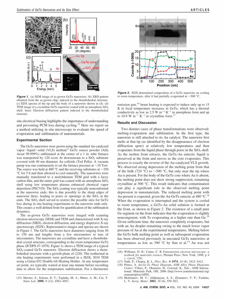
When the evaporation is interrupted and the system is cooledto room temperature, a GeTe-Au solid solution is formed atthe front, as shown in Figure 2. The existence of a small pureGe segment on the front indicates that the evaporation is slightlynoncongruent, with Te evaporating at a higher rate than Ge.19
Given sufficient time, the nanowire completely evaporates, butwith an Au droplet remaining owing to the much lower vaporpressure of Au at the experimental temperatures. Melting belowthe GeTe bulk melting point as well as subsequent evaporationhas been observed previously in uncoated GeTe nanowires attemperatures as low as 390 °C by Sun et al.14 Au was not
(15) Meister, S.; Schoen, D. T.; Topinka, M. A.; Minor, A. M.; Cui, Y.Nano Lett. 2008, 8 (12), 4562–4567.
(16) Williams, D. B.; Carter, C. B Transmission electron microscopy: atextbook for materials science; Plenum Press: New York, 1996; p 4v. (xxvii, 729).
(17) Nath, P.; Chopra, K. L. Phys. ReV. B 1974, 10 (8), 3412–3412.(18) Prince, A. Au-Ge-Te Phase Diagram, ASM Alloy Phase Diagrams
Center; Villars, P., Okamoto, H., Cenzual, K., Eds.; ASM Interna-tional: Materials Park, OH, 2006 (http://www.asminternational.org/asmenterprise/APD).
(19) Molchanov, M. V.; Alikhanyan, A. S.; Zlomanov, V. P.; Yashina,L. V. Inorg. Mater. 2002, 38 (6), 559–563.
Figure 1. (a) SEM image of as-grown GeTe nanowires. (b) XRD patternobtained from the as-grown chip, indexed to the rhombohedral structure.(c) EDX spectra of the tip and the body of a nanowire shown in (d). (d)TEM image of a crystalline GeTe nanowire coated with an amorphous SiO2
shell. Inset: Electron diffraction pattern indexed to the rhombohedralstructure.
Figure 2. EDX-determined composition of a GeTe nanowire on coolingto room temperature, after it had partially evaporated at ∼500 °C.
J. AM. CHEM. SOC. 9 VOL. 131, NO. 40, 2009 14527
Sublimation of GeTe Nanowires and Its Size Effect A R T I C L E S

indicated as a significant player in those experiments. Thecorrelation of low melting point to Au-presence in our workdoes not preclude the suppression of the melting point by othermeans; however in our experiments on nanowires with diametersranging from 90 to 200 nm, the Au eutectic completelydominated low temperature melting dynamics.
A different type of behavior was observed when the activatedpart of nanowire does not contain Au (the Au tip was on theother end or lost during nanowire transfer). The nanowire startssublimating at relatively low temperatures, and distinct facetsof the solid-vapor interface can be seen (see below). Givensufficient time, the GeTe core sublimates away and vanishescompletely with no particles remaining. The following discus-sion focuses on this second type of behavior: sublimation ofpure GeTe.
As the GeTe core sublimates isothermally, an empty SiO2
tube remains due to the much lower vapor pressure of the oxide.This process can be seen from Figure 3a and a video includedin the Supporting Information. The GeTe core sublimatescontinuously and the vapor-phase molecules are transportedalong the oxide tube and escape from the end. The mean freepath of the evaporated molecules/atoms can be estimated using
l ∼ kBT/[d2 ·Pv(T)], where d is the effective diameter of themolecules/atoms and Pv(T) is the equilibrium vapor pressure. lis calculated to be >10 µm for our experimental conditions,which is much larger than the diameter (D ∼ 100 nm) butcomparable to the length (L ∼ 10 µm) of the nanowiresinvestigated.
This system mimics thermal effusion cells used in depositionof thin films. In the widely used Knudsen cell,20 the orifice issufficiently small such that the pressure inside the cell can reachthe equilibrium vapor pressure of the condensed phase withoutbeing significantly reduced by effusion. At equilibrium, on theinterface between the condensed and the vapor phases, the netflux of molecules leaving the condensed phase is equal to theflux joining it from the vapor. This is given by the impinge-ment flux in the ideal gas law
where A ) π(D/2)2 is the exposed surface area and m is themolecular mass. In the present nanoscale “cell”, however, thevapor is transported following different kinetics as such balanceis broken, and thus cannot be treated with the equilibrium model.The opposite of Knudsen-type is Langmuir-type, that is, directsublimation into vacuum from the surface of the condensed
(20) Smith, D. L. Thin-film deposition: principles and practice; McGraw-Hill: New York, 1995.
Figure 3. (a) TEM video frames of two GeTe/SiO2 nanowires undergoingsublimation at 469 °C. The inner diameters of the upper and lower wiresare 100 and 130 nm, respectively. The sublimation fronts are distinctlyfaceted. A video of this process is included in the Supporting Information.(b) Schematic phase diagram showing the GeTe nanowire sublimation ormelting-evaporation process, (upper and lower, respectively, pictured asdashed arrows). (c) Measured R ·Pv of GeTe nanowires (open circles) plottedas a function of temperature together with partial vapor pressures of bulkGeTe [Molchanov et al.]. Also shown are the R ·Pv at early stage (solidsquare) and final stage (solid triangle) estimated for the nanoparticlesublimation in Figure 4. The TEM chamber base pressure was ∼10-8 torr.
Figure 4. (a) Sequential snapshots of a GeTe nanoparticle sublimatingisothermally (at 512 °C) from an oxide shell. The inner diameter of theshell is 90 nm. A video of this process is included in the SupportingInformation. (b) Average dimension of the GeTe nanoparticle shown in (a)as a function of time, showing two distinct linear regions, the second ofwhich kicks in at sub-30 nm dimensions.
J0 )Pv(T)A
√2πmkBT(1)
14528 J. AM. CHEM. SOC. 9 VOL. 131, NO. 40, 2009
A R T I C L E S Yim et al.

phase.21,22 In this case, there is no flux from the vapor recon-densing, and the material sublimates with a flux of
where R is the vaporization coefficient. In an attempt to quantifythe sublimation process, we treat the nanowire sublimation inthe Langmuir-type kinetics. In this approximation, the sublima-tion flux must be related to the material loss rate through
where x(t) is the remaining nanowire core length and F is themolecular density (molecules/volume). Therefore, the GeTe corelength decreases according to
Thus the GeTe core should vanish at a constant, temperature-dependent rate. It was shown, using mass spectrometry, thatbulk GeTe evaporates approximately congruently, with GeTemolecules as the main vapor species and Te2 molecules the nextabundant composition at ∼1/10 the concentration of the GeTemolecules.19 The reported partial vapor pressure of GeTe andTe2 are plotted in Figure 3c, showing an Arrhenius dependenceon temperature with an evaporation enthalpy of ∼188 kJ/mol.19
Assuming predominantly congruent sublimation, R ·Pv(T) ofGeTe can be determined using eq 4. It is clear from Figure 3cthat R ·Pv(T) of the GeTe nanowires is about 3 orders ofmagnitude lower than Pv(T) of bulk GeTe. However, they followapproximately the same Arrhenius dependence on temperature.These results indicate that the enthalpy is approximately thesame as for the bulk, and the vaporization coefficient of theGeTe nanowires is R ≈ 10-3 assuming the same Pv(T) as thatof the bulk. As a Langmuir-type sublimation has been assumed,this value sets the lower limit for the real vaporizationcoefficient.
Sublimation of bulk crystals was studied extensively formetals and compounds in the 1950s-1970s. At equilibrium,the molecule flux impinging on the crystal surface, Ji, is equalto J0 given by eq 1. However, the sublimation flux Jv is smallerthan J0 by a factor of R according to eq 2. Surface atomssublimate predominantly from active spots (mainly atomicledges and crystal edges) where the desorption energy is thelowest.21 Surface atoms at other locations must either thermallydiffuse to the ledges, or wait for a ledge to move by. In Knudsen-type sublimation (equilibrium), Ji and Jv are balanced througha third term, the reflection flux, that describes a stickingcoefficient of impinging atoms lower than unity. In Langmuir-type sublimation (into vacuum) where Ji ) 0, Jv can beexperimentally measured by thermogravimetric methods andused to determine R. For nanosized materials, however, ther-mogravimetric analysis is difficult. In this case, in situ imagingof the vaporization process provides an alternative way toquantify R. For most materials with clean surfaces, R was
measured to be equal or close to unity. R much lower than unitycould be caused by various effects, such as limited surfaceatomic diffusion, ledge motion kinetics, entropy restraints insublimation, and surface contamination.21 Using the surfacediffusion limited scenario, one expects23
which is ≈Xj/λj at small R. Here λj and Xj are the average spacingbetween active spots and mean diffusion length of surface atoms,respectively. R ≈ 10-3 in the GeTe nanowire sublimationimplies that Xj/λj ∼ 10-3; that is, active sites are extremely widelyspaced relative to the atom diffusion lengths. Given the lowsublimation temperature, Xj is estimated to be on the order ofthe interatomic distance, ∼3 Å, giving rise to λj ∼ 300 nm.Considering that the total exposed dimension of the GeTenanowires is the diameter (<300 nm), this indicates that (i) theatoms mostly sublimate from a small number of active spots,presumably atomic ledges initiated at the edge of the exposednanowire cross section, and (ii) other effects may also play animportant role in limiting the sublimation. For example, a highactivation energy for dissociation at the active spots wassuggested to explain R ≈ 10-7 for red phosphorus and NH4Clby Hirth et al.21 and Spingler,24 respectively. Alternatively,minute surface contamination was used to explain a reductionof R from 1 to 10-3 in evaporation of Hg by Knudsen.25 Thismechanism cannot be ruled out in the present work. The lowvalue of R quantified in this work indicates a relatively lowmaterial loss rate from GeTe nanowires. This result is usefulfor designing and operating GeTe-based nanoscale memorydevices, as these devices are typically operated at high localtemperatures.
As a result of the narrow range of nanowire diameters studiedin the in situ heating experiments (90-200 nm), we did notobserve a systematic dependence on the nanowire diameter inR. However, the final stage of the sublimation of GeTenanowires without Au tips can provide a glimpse of the phasetransition dynamics at reduced dimensions. At the final stageof sublimation, the remaining GeTe can be treated as ananoparticle with size smaller than the diameter of the nanowire(∼100 nm). Tracking the GeTe particle as it vanishes allowsus to study the effect of size on sublimation. A typical vanishingprocess is shown in Figure 4a, and a video is in the SupportingInformation. The GeTe particle has a nonspherical shapethroughout the process, indicating that it is subliming from thesolid phase. To quantify the sublimation dynamics, we ap-proximate the volume of the GeTe particle by ∼S3/2 where S isthe projected area of the particle in the TEM image. The surfacearea of the particle is ∼S and an average dimension of theparticle can be defined as L ∼ S1/2. We can analyze thesedynamics using eqs 2 and 3 by replacing A with S and x withL, which again yields eq 4 giving L(t) as a linear function. Figure4b shows L as a function of time, where two distinct linearslopes can be discerned. The values of R determined using theslopes for the early and final stages are plotted in Figure 3.Compared with R ≈ 10-3 of nanowires, it can be seen that thenanoparticle has higher values of R, ranging from 5 × 10⁻³ atthe early stage to 2 × 10⁻² at the final stage. Although this
(21) Hirth, J. P.; Pound, G. M. Condensation and eVaporation: nucleationand growth kinetics, Macmillan: New York, 1963.
(22) Surek, T.; Pound, G. M.; Hirth, J. P. J. Chem. Phys. 1971, 55 (11),5157–5163.
(23) Hirth, J. P.; Pound, G. M. J. Phys. Chem. 1960, 64 (5), 619–626.(24) Spingler, H Z. Phys. Chem 1942, 52B, 90.(25) Knudsen, M. Ann. Phys. 1915, 352 (13), 697–708.
Jv )R · Pv(T)A
√2πmkBT) R · J0 (2)
Jv ) F · A · dxdt
(3)
x(t) )R · Pv(T)
F√2πmkBT· (t0 - t) (4)
R ∼ tanh(λ̄/Xj)
λ̄/Xj(5)
J. AM. CHEM. SOC. 9 VOL. 131, NO. 40, 2009 14529
Sublimation of GeTe Nanowires and Its Size Effect A R T I C L E S

conclusion is only semiquantitative due to scattering in experi-mental data and errors in estimation of the particle geometry,we believe that this shows evidence of increased R for trulynanosized GeTe. This is consistent with eq 5, because as theGeTe particle shrinks in size, the surface is expected to developa higher density of ledges and high-index facets, resulting anincreased λj and consequently higher R. A full quantification ofthis size effect requires a systematic investigation of nanosizedparticle sublimation.
Conclusions
In summary, we have demonstrated that nanoscale sublima-tion and evaporation can be quantified for a well-definedmaterial geometry using in situ TEM. Melting and sublimationof GeTe nanowires at temperatures below the bulk melting pointhave been observed. The vaporization coefficient of GeTenanowires was evaluated to be approximately 10-3. At suf-ficiently small dimensions, the sublimation rate increases aspredicted from classical sublimation theory. With the intenselocal temperatures required to set/reset the PCM, control of
sublimation and evaporation is of critical importance in deter-mining the viability of nanoscale PCM devices.
Acknowledgment. The authors thank Prof. A. Stacy of U.C.Berkeley for the use of the diffractometer. We are grateful fortechnical assistance from C. Song, Z. Lee, and Prof. A. Minor.This work was supported in part by National Science Foundationunder Grant No. EEC-0425914 and in part by the LaboratoryDirected Research and Development Program of Lawrence BerkeleyNational Laboratory (LBNL) under the Department of EnergyContract No. DE-AC02-05CH11231. J.Y. acknowledges supportfrom the National Science Foundation - Graduate Research Fel-lowship Program. Portions of this work were performed at theNational Center for Electron Microscopy, LBNL, and the U.C.Berkeley Microfabrication Laboratory.
Supporting Information Available: Videos of nanowire andnanoparticle sublimation captured during in situ TEM andassociated captions. This material is available free of chargevia the Internet at http://pubs.acs.org.
JA905808D
14530 J. AM. CHEM. SOC. 9 VOL. 131, NO. 40, 2009
A R T I C L E S Yim et al.