su-8 micromachined terahertz waveguide circuits …etheses.bham.ac.uk/3087/1/shang11phd.pdfi the...
TRANSCRIPT

i
THE UNIVERSITY OF BIRMINGHAM
SU-8 Micromachined Terahertz Waveguide Circuits and Coupling Matrix Design of
Multiple Passband Filters
Xiaobang Shang
A thesis submitted to the University of Birmingham for the degree of Doctor of Philosophy
School of Electronic, Electrical and Computer Engineering The University of Birmingham
October 2011

University of Birmingham Research Archive
e-theses repository This unpublished thesis/dissertation is copyright of the author and/or third parties. The intellectual property rights of the author or third parties in respect of this work are as defined by The Copyright Designs and Patents Act 1988 or as modified by any successor legislation. Any use made of information contained in this thesis/dissertation must be in accordance with that legislation and must be properly acknowledged. Further distribution or reproduction in any format is prohibited without the permission of the copyright holder.
ii
Abstract
This thesis presents the designs and measurement performance of nine SU-8 micromachined
waveguide circuits operating at WR-10 band (75-110 GHz), WR-3 band (220-325 GHz) and WR-1.5
band (500-750 GHz). Two thick SU-8 photoresist micromachining processes, namely, the separate
single-layer process and the joint two-layer process, are developed to fabricate these terahertz
waveguide circuits. In order to achieve accurate and secure interconnections with measurement
network analyzers, two calibrated measurement methods for micromachined waveguide circuits are
proposed. The first measurement method is achieved by employing a pair of embedded H-plane back-
to-back bends, which are connected at the two ends of the micromachined waveguide circuits. The
bend structures are specially designed to offer a good match over a wide frequency range. The second
measurement technique employs a conventionally machined metal block constructed with two
separate pieces in which to mount the micromachined circuit. A choke flange is adopted to eliminate
the effect of air gaps at the interfaces between the micromachined circuits and the metal block. The
measurement performance of these micromachined circuits is excellent in terms of very low insertion
loss.
The design of multiple-passband filters using coupling matrix optimisation is also discussed in this
thesis. The optimisation is performed on the coupling matrix and a genetic algorithm (GA) is
employed to generate initial values for the control variables for a subsequent local optimisation
(sequential quadratic programming - SQP search). The novel cost function presented in this thesis
measures the difference of the frequency locations of reflection and transmission zeros between the
response produced by the coupling matrix and the ideal response. This cost function eliminates the
need of weighing functions, which yield faster and more reliable convergence of the optimisation.
Four prototype filters with responses from dual-band to quad-band are given as examples. An eighth-
order X-band dual-band waveguide filter with all capacitive coupling irises is fabricated and measured
to verify the design technique. Excellent agreement between simulation and experimental result is
achieved.

iii
Acknowledgements
I would like to thank my supervisor Prof. Mike J. Lancaster for his instructive ideas, patient
mentoring and continuous support during my Ph.D. study in the University of Birmingham. Without
his assistance and encouragement, the work presented in this thesis may never have been
accomplished. I am also grateful to my co-supervisor Dr. Fred Huang for his valuable comments on
my Ph.D. work and progress reports.
My appreciation also goes to my colleagues in the Emerging Device Technology Research Group at
the University of Birmingham for their support and friendship over these three years. In particular, I
would like to thank Dr. Yi Wang for many useful discussions on the filter design, Dr. Maolong Ke for
fabricating all the SU-8 devices presented in this thesis, Dr. Tim Jackson for his precious advice and
comments on my progress reports and my final Ph.D. thesis and Dr. Yudong Wu for his suggestions
and encouragement.
I also appreciate the financial support from the U.K. Overseas Research Student (ORS) Scholarship
and the Engineering School Scholarship of the University of Birmingham.
The microwave measurement student fellowship awarded by the Automatic RF Techniques Group
(ARFTG), and the financial assistance provided by ARFTG, are also greatly appreciated.
Last but certainly not least I want to express my great gratitude to my parents and all of my friends for
their invaluable support and encouragement.

iv
Table of Contents
Chapter 1: Introduction .......................................................................................................... 1
1.1 Motivation and Objectives ............................................................................................... 1 1.2 Thesis Overview .............................................................................................................. 2 References .............................................................................................................................. 4
Chapter 2: Fundamental Theory of Resonator Filters and Waveguides ........................... 5
2.1 Overview of Microwave Filters ....................................................................................... 5 2.2 Filter Transfer Functions .................................................................................................. 7
2.2.1 All-pole Chebyshev filters ........................................................................................ 7 2.2.2 Filters with finite transmission zeros ........................................................................ 9 2.2.3 Linear phase filters .................................................................................................. 11
2.3 Coupling Matrix Representation .................................................................................... 14 2.4 Physical Realization Using Waveguide Technology ..................................................... 20
2.4.1Rectangular waveguide ............................................................................................ 20 2.4.2 Waveguide cavities ................................................................................................. 23
2.5 Design of Iris Coupled Waveguide Resonator Filters ................................................... 25 2.5.1 Calculation of external quality factors .................................................................... 27 2.5.2 Calculation of inter-resonator couplings ................................................................. 29 2.5.3 Final optimisation ................................................................................................... 31
2.6 Conclusions .................................................................................................................... 33 Reference ............................................................................................................................. 33
Chapter 3: Micromachining.................................................................................................. 34
3.1 Terahertz Applications ................................................................................................... 35 3.2 Terahertz Waveguide Circuits ....................................................................................... 39
3.2.1 Conventional machining ......................................................................................... 39 3.2.2 Micromachining ...................................................................................................... 40
3.3 Separate SU-8 Single-Layer Fabrication Process .......................................................... 50 3.3.1 General SU-8 fabrication process ........................................................................... 50 3.3.2 Process discussions ................................................................................................. 56
3.4 Fully Joined SU-8 Two-Layer Fabrication Process ....................................................... 63 3.5 Conclusions .................................................................................................................... 67 References ............................................................................................................................ 68
Chapter 4: Micromachined Waveguide Circuits Measured with Bends .......................... 70
4.1 Literature Review........................................................................................................... 70 4.2 Principles of Bend Measurement Method ...................................................................... 75 4.3 Micromachined WR-10 Band Components With Bends ............................................... 76
4.3.1 WR-10 band waveguide .......................................................................................... 77 4.3.2 WR-10 band filter ................................................................................................... 82

v
4.3.3 Discussion of capacitive iris coupled waveguide filters ......................................... 86
4.4 Micromachined WR-3 Band Components With Bends ................................................. 89 4.4.1 WR-3 band through waveguide .............................................................................. 89 4.4.2 WR-3 band single band filter .................................................................................. 93 4.4.3 WR-3 band dual-band filter .................................................................................... 98
4.5 Micromachined WR-1.5 Band Filter ........................................................................... 101 4.6 Conclusions .................................................................................................................. 104 References .......................................................................................................................... 104
Chapter 5: Micromachined Waveguide Circuits Measured with Block......................... 106
5.1 Principles of Block Measurement Method .................................................................. 106 5.2 Waveguide Choke Rings and PBG Connectors ........................................................... 108
5.2.1 Photonic bandgap structure ................................................................................... 109 5.2.2 Choke flange ......................................................................................................... 111
5.3 WR-3 Band Circuits From SU-8 Single-Layer Process .............................................. 115 5.3.1 WR-3 band through waveguide ............................................................................ 115 5.3.2 WR-3 band single band filter ................................................................................ 120
5.4 WR-3 Band Circuits From SU-8 Two-Layer Process ................................................. 124 5.4.1 WR-3 band through waveguide ............................................................................ 124 5.4.2 WR-3 band single band filter ................................................................................ 126 5.4.3 WR-3 band dual-band filter .................................................................................. 128
5.5 Conclusions .................................................................................................................. 129 References .......................................................................................................................... 130
Chapter 6: The Design of Multiple-Passband Filters using Coupling Matrix
Optimisation ......................................................................................................................... 132
6.1 Introduction .................................................................................................................. 132 6.2 Multi-Band Filter Polynomial Transfer Function Synthesis ........................................ 133 6.3 Coupling Matrix Optimisation ..................................................................................... 139
6.3.1 Cost function for coupling matrix optimisation .................................................... 140 6.3.2 Calculation of external quality factor ................................................................... 144 6.3.3 Coupling matrix optimisation flowchart ............................................................... 145 6.3.4 Examples of coupling matrix optimisation ........................................................... 148 6.3.5 Further discussions................................................................................................ 159
6.4 Practical Implementation of A Dual-Band Filter ......................................................... 166 6.5 Conclusions .................................................................................................................. 173 References .......................................................................................................................... 173
Chapter 7: Conclusions and Future Work ........................................................................ 177
7.1 Conclusions .................................................................................................................. 177 7.2 Future Work ................................................................................................................. 184 References .......................................................................................................................... 184
Appendix I: Multi-Band Filter Polynomial Synthesis ..................................................... 186

vi
Appendix II: Publications ................................................................................................... 203
1
Chapter 1
Introduction
This thesis is intended to present the work which can be broadly grouped into two separate categories:
(i) SU-8 micromachined terahertz waveguide circuits; (ii) design of coupling matrices for multiple
passband filters using optimisation.
1.1 Motivation and Objectives
There is an increasing interest in the terahertz spectrum due to its promising applications such as
medical imaging, security scanning and communications in space or high-altitude earth atmosphere
[1]. However, as the circuits’ operating frequencies go up into terahertz region, conventional CNC
(computer numerical controlled) machining is no longer a good choice for the fabrication of
waveguide circuits due to its limited dimensional accuracy, lack of ability for large scale production
and relatively high cost [2]. In the past few decades, a wide range of micromachining techniques have
been proposed and developed to fabricate these terahertz waveguide circuits with improved
dimensional accuracy and reduced cost. Among these micromachining techniques, the thick SU-8
photoresist process has attracted the most attention due to its (i) high achievable structure aspect ratio
(>15:1) [3]; (ii) relative low cost processing procedure [2]; (iii) capability of building photoresists
with thickness from 1 µm to 2 mm [4]; (iv) nearly vertical sidewalls [5]. The work presented in this
thesis is to investigate the application of thick SU-8 micromachining technique to the fabrication of
terahertz waveguide components. The optimisation of the fabrication process, the designs of
waveguide circuits compatible with the micromachining process, and the investigation of reliable
measurement techniques are three major objectives of this research project.
Recently multi-band filters have been studied extensively to meet the increasing demands in areas
such as satellite systems and modern communication systems where non-contiguous channels are
transmitted to the same geographic area through one beam [6]. Compared with the power
splitter/combiner configuration, a multi-band filter is capable of providing multiple passbands using a
single component. This simplifies the circuit design and reduces the size and mass of the overall

2
system. One of the main challenges in multi-band filter design is the calculation of the coupling
matrix that fulfils the filter’s complex specifications. Two types of coupling matrix design techniques
for multi-band filter are reported in literature. They are (i) methods based on optimisation; (ii)
techniques based on synthesis. In this work, the coupling matrix design approach based on
optimisation is chosen and investigated mainly due to its three advantages over the latter one: (i) it is
capable of dealing with filters with arbitrary desired topologies; (ii) it is straightforward to control the
signs and values of certain specified coupling coefficients in the optimisation algorithm; (iii) it is
easier for the end-user to operate. The principle objective of this work is to obtain an efficient and
robust coupling matrix optimisation programme, which can be applied to generate coupling matrices
for cross-coupled filters with large number of resonators, complex magnitude/phase responses and
various coupling topologies.
1.2 Thesis Overview
This thesis has seven chapters, which are intended to present two parts of work: (i) SU-8
micromachined terahertz waveguide circuits; (ii) coupling matrix design of multi-band filters using
optimisation. Chapters 3 to 5 comprise the first part, whereas Chapter 6 in conjunction with Appendix
I forms the second part of this thesis. These seven chapters are organized as follows.
Chapter 1 is devoted to presenting the motivation and objectives of the work described in this thesis.
This chapter also includes an overview of the thesis structures.
Chapter 2 provides the fundamental theories required by the work presented in the following chapters.
It begins with an introduction of basic concepts of microwave filters. Two representation methods for
filters, i.e. transfer function polynomials and the coupling matrix, are explained in this chapter. This
is followed by an overview of waveguide technology, more specifically to the introduction of
waveguide losses, unloaded quality factors and resonant frequencies of waveguide cavities. In the
final part of this chapter, the design of a 300 GHz Chebyshev bandpass waveguide filter is described
in detail as an example.

3
In Chapter 3, the manufacturing techniques (mainly micromachining) for terahertz waveguide circuits
are discussed. It begins with an introduction of the promising applications of terahertz spectrums. This
is followed by a review of popular micromachining techniques for the fabrication of terahertz circuits.
The final part of this chapter focuses on the detailed description of two thick SU-8 micromachining
processes, which are developed in the EDT research group and employed in the work presented in this
thesis.
Chapter 4 presents the SU-8 micromachined waveguide circuits measured with a pair of H-plane
back-to-back bends. Both the bends and the metal block (discussed in Chapter 5) are employed to help
the measurements of these SU-8 micromachined waveguide circuits. The principles of the bend
measurement technique are explained first. Then the designs and measurement performance of six
SU-8 waveguide circuits (i.e. through waveguides and filters), integrated with a pair of H-plane bends,
operating at WR-10 band (75-110 GHz) and WR-3 band (220-325 GHz), are described in detail. The
design of a WR-1.5 band (500-750 GHz) third order bandpass filter is provided in the final part of this
chapter. This chapter also includes a literature review of some micromachined waveguide circuits that
work at the frequencies range from WR-10 band to WR-3 band.
Chapter 5 deals with the SU-8 micromachined waveguide circuits that are mounted in a metal block
during measurement. It starts by explaining the principles of the metal block measurement method.
This is followed by a discussion of three WR-3 band SU-8 waveguide circuits. This chapter also
includes a discussion of a waveguide choke flange and a photonic bandgap structure, both of which
are proposed to address the issues of air gaps at the joints between the metal block and SU-8 circuits.
Chapter 6 presents a coupling matrix design approach for multi-band bandpass prototype filters. This
design technique is divided into two major steps: (i) the synthesis of the characteristic polynomials; (ii)
the optimisation of non-zero coupling coefficients. These two steps are explained in succession in this
chapter. Then four design examples with different emphasises are demonstrated. In the last part of this
chapter, an eighth order X-band dual-band waveguide filter is presented to verify the design approach.

4
Chapter 7 concludes the whole thesis. In this chapter, comparisons between two different SU-8
fabrication processes described in Chapter 3, as well as comparisons between two different
measurement techniques described in Chapters 4 and 5, are presented in detail. This chapter also
includes a comparison between the SU-8 micromachining work presented in this thesis and other
published micromachining work. The second part of this chapter outlines the main novelties of the
coupling matrix optimisation work presented in Chapter 6. Suggestions to the future work are
included in the final part of this chapter.
References
[1] Dobroiu A., Otani C., Kawase K.: ‘Terahertz-Wave Sources and Imaging Applications,’
Measurement-Science and Technology, 2006, 17, pp. 161-174
[2] Lancaster M. J., Zhou J., Ke M. L., Wang Y., Jiang K.: ‘Design and High Performance of a
Micromachined K -Band Rectangular Coaxial Cable,’ IEEE Transactions on MTT, 2007, 55, 7, pp.
1548-1553
[3] Biber S., Schur J., Hofmann A., Schmidt L. P.: ‘Design of New Passive THz Devices Based on
Micromachining Techniques.’ MSMW Symposium Proceeding, June 2004, pp. 26-31.
[4] Conradie E. H., Moore D. F.: ‘SU-8 Thick Photoresist Processing as A Functional Material for
MEMS Applications,’ Journal of Microw. and Microenginnering, 2002, 12, pp. 368-374
[5] Ke M., Shang X., Wang Y., Lancaster M. J.: ‘Improved Insertion Loss for a WR-3 Waveguide
Using Fully Cross-Linked Two-layer SU8 Processing Technology,’ the 12th International Symposium
on RF-MEMS and RF-Microsystems (MEMSWAVE 2011), Athens, Greece, June 27-29, 2011
[6] Lee J., Sarabandi K.: ‘A Synthesis Method for Dual-Passband Microwave Filters,’ IEEE
Transactions on MTT, 2007, 55, 6, pp.1163-1170
5
Chapter 2
Fundamental Theory of Resonator Filters and Waveguides
2.1 Overview of Microwave Filters
A microwave filter is a two-port network employed to transmit and attenuate signals in specified
frequency bands. Microwave filters have wide applications in communication systems, radar systems
and laboratory measurement equipments [1].
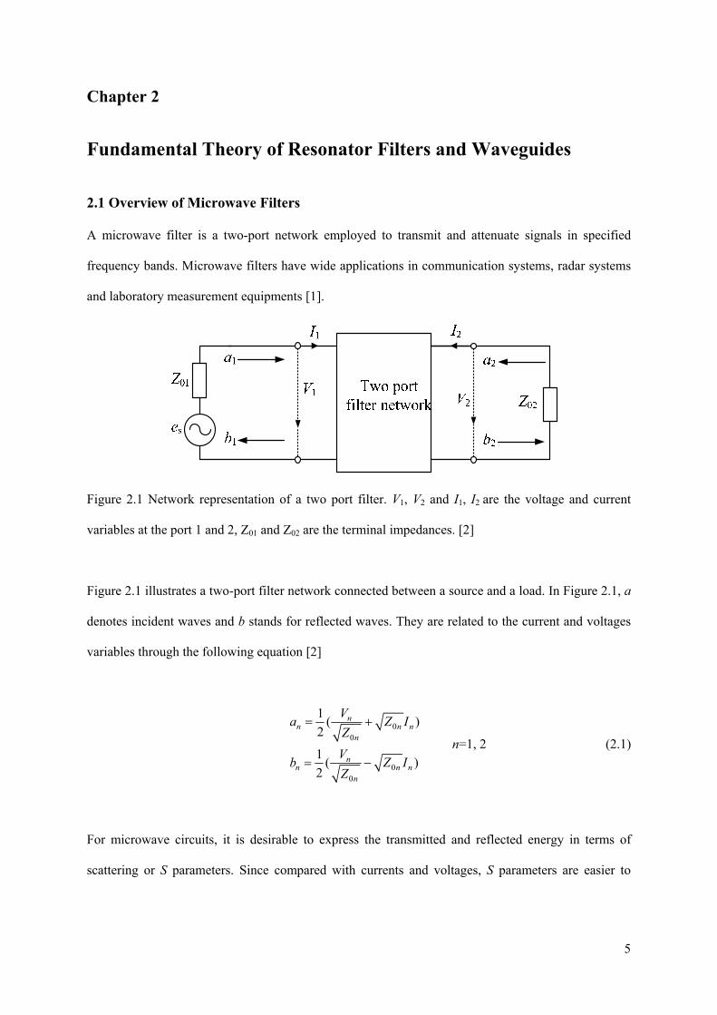
Figure 2.1 Network representation of a two port filter. V1, V2 and I1, I2 are the voltage and current
variables at the port 1 and 2, Z01 and Z02 are the terminal impedances. [2]
Figure 2.1 illustrates a two-port filter network connected between a source and a load. In Figure 2.1, a
denotes incident waves and b stands for reflected waves. They are related to the current and voltages
variables through the following equation [2]
00
00
1( )
2
1( )
2
nn n n
n
nn n n
n
Va Z I
Z
Vb Z I
Z
n=1, 2 (2.1)
For microwave circuits, it is desirable to express the transmitted and reflected energy in terms of
scattering or S parameters. Since compared with currents and voltages, S parameters are easier to

6
measure and work with at high frequencies [3]. The S parameters of the filter network shown in
Figure 2.1 can be expressed as [2]
2 1
2 1
1 111 12
1 20 0
2 221 22
1 20 0
a a
a a
b bS S
a a
b bS S
a a
(2.2)
The parameter S11 is the reflection coefficient looking into port 1, when port two is terminated with a
matched load (i.e. a2=0). The parameter S21 is the transmission coefficient from port 1 to port 2.
Similarly, S12 is the transmission coefficient from port 2 to port 1, and S22 is the reflection coefficient
seen at port 2 when port 1 is terminated in a matched load (i.e. a1=0). In this work, the prototype filter
network is assumed to be reciprocal (i.e. S21=S12), symmetric (i.e. S11=S22) and lossless (|S11|2+|S21|
2=1).
Typically, filters are specified using their amplitude and phase or group delay responses. For
amplitude responses, the transmission loss (LA) and return loss (LR) are defined as
A 21
R 11
20log(| |) dB
20log(| |) dB
L S
L S
(2.3)
where the logarithm operation is base 10. In this thesis both the transmission loss and the return loss
are assumed to be positive. For a lossless filter network (i.e. |S11|2+|S21|
2=1), LA and LR are related as
R
A
/10A
/10R
10log(1 10 ) dB
10log(1 10 ) dB
L
L
L
L
(2.4)
Normally, the phase response of a filter is characterized by its group delay (τ), which is defined as [2]
21 secondsd
d
(2.5)

7
where ϕ21 (in radians) is the phase of the S21 and ω is the angular frequency. Group delay represents
the actual time delay of the transmitted signal passing through the filter.
2.2 Filter Transfer Functions
The design of a microwave filter starts with developing a low-pass prototype filter normalised in
terms of centre frequency, bandwidth and impedance [3]. This normalisation simplifies the design of
the practical filter regardless of its frequency range, impedance and type (low-pass, high-pass,
bandpass, or bandstop) [3]. Then the desired filter responses (for instance bandpass) can be achieved
through a low-pass to bandpass frequency transformation. This section explores the transfer functions
of some classical low-pass prototype filters.
2.2.1 All-pole Chebyshev filters
The filter with Cheyshev responses shows an equal-ripple passband and a maximally flat stop-band
[2]. The amplitude-squared transfer function for a lossless filter with Cheyshev responses is defined as
221 2 2
1| ( ) |
1 ( )n
S jT
(2.6)
where Ω is the angular frequency, ɛ is the ripple constant, which can be determined from the
passband ripple LAr (in dB) as
Ar
1010 1L
(2.7)
Tn(Ω) is the Chebyshev polynomial and it can be expressed as [2]
8
1
1
cos( cos ) | | 1( )
cosh( cosh ) | | 1n
nT
n
(2.8)
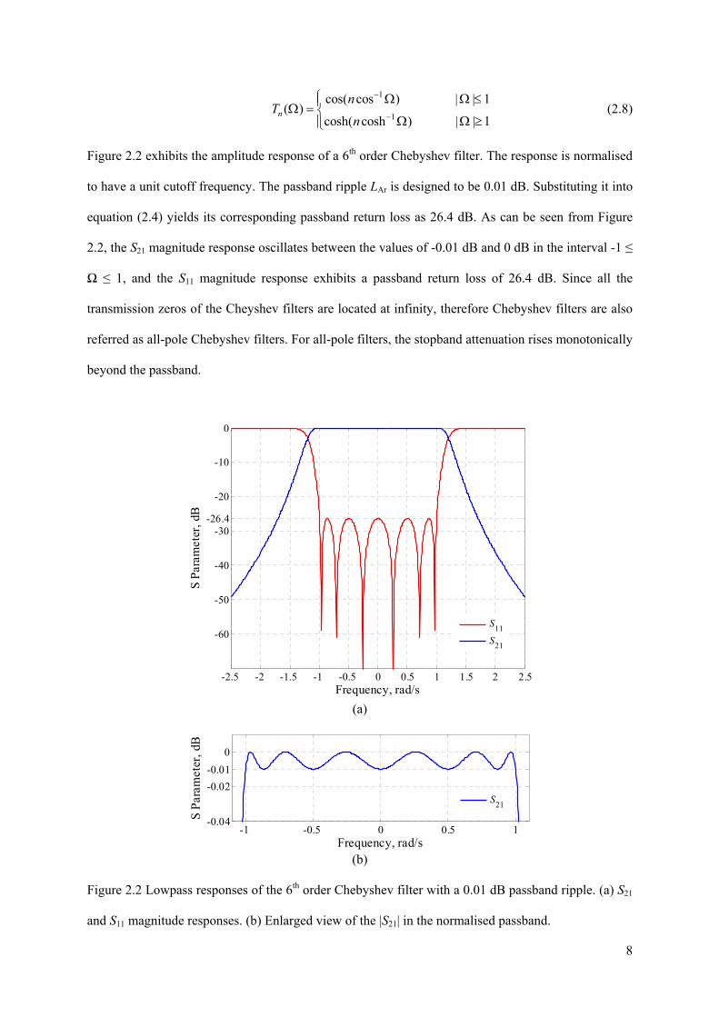
Figure 2.2 exhibits the amplitude response of a 6th order Chebyshev filter. The response is normalised
to have a unit cutoff frequency. The passband ripple LAr is designed to be 0.01 dB. Substituting it into
equation (2.4) yields its corresponding passband return loss as 26.4 dB. As can be seen from Figure
2.2, the S21 magnitude response oscillates between the values of -0.01 dB and 0 dB in the interval -1 ≤
Ω ≤ 1, and the S11 magnitude response exhibits a passband return loss of 26.4 dB. Since all the
transmission zeros of the Cheyshev filters are located at infinity, therefore Chebyshev filters are also
referred as all-pole Chebyshev filters. For all-pole filters, the stopband attenuation rises monotonically
beyond the passband.
(a)
(b)
Figure 2.2 Lowpass responses of the 6th order Chebyshev filter with a 0.01 dB passband ripple. (a) S21
and S11 magnitude responses. (b) Enlarged view of the |S21| in the normalised passband.
-2.5 -2 -1.5 -1 -0.5 0 0.5 1 1.5 2 2.5
-60
-50
-40
-30
-20
-10
0
-26.4
Frequency, rad/s
S P
aram
eter
, dB
S11
S21
-1 -0.5 0 0.5 1-0.04
-0.02
0
-0.01
Frequency, rad/s
S P
aram
eter
, dB
S21

9
2.2.2 Filters with finite transmission zeros
For filters with transmission zeros at finite frequencies, it is preferable to express the filter’s scattering
parameters, S11(s) and S21(s), in terms of the ratio of two polynomials, as [3]:
11
( )( )
( )
F sS s
E s 21
( )( )
( )
P sS s
E s (2.9)
F(s) and E(s) are Nth-degree polynomials with highest-power coefficients equal to one. P(s) has also
been normalized to its highest-power coefficient and its order is the same as the number of
transmission zeros at finite frequencies. ε is a real constant and it is used to normalise the polynomial
P(s). ε is computed by evaluating P(s)/E(s) at a special frequency (for instance band edge frequency),
where |S21(s)| is known. From equation (2.9) it is readily seen that the roots of P(s) and F(s)
correspond to the filter’s transmission zeros (sTzP) and reflection zeros (sRzP), respectively. The filter
poles (sPP) common to S11(s) and S21(s) correspond to the roots of E(s). The relationships between the
normalised polynomials and the positions of zeros and poles are established with the following
equations:
TZ
TzP
zP
P
1
R
1
P
1
( ) ( )
( ) ( )
( ) ( )
N
i
N
i
N
i
P s s s
F s s s
E s s s
(2.10)
where N is the number of resonators and NTZ is the number of finite transmission zeros (NTZ ≤ N-2).
This calculation will lead to a unit leading coefficient (i.e. coefficient of the term with highest power
of s) for these three polynomials. From the filter’s specifications, a wide range of methods are
available to obtain the desired frequency locations of the zeros and poles. Then the characteristic
polynomials of the filter can be constructed using equation (2.10). A detailed review of these
polynomial generation methods is provided in Chapter 6.

10
Typically, finite transmission zeros are introduced to increase the selectivity of the filter’s amplitude
response. Figure 2.3 plots the magnitude responses of a 6th order general Chebyshev filter with a pair
of transmission zeros located at ±j1.5. The passband return loss of this filter is designed to be 26.4 dB,
which is the same as the 6th order all-pole Chebyshev filter shown in Figure 2.2. As can be observed
from Figure 2.3 (b), by introducing finite transmission zeros, increased selectivity has been achieved
at the frequencies near the passband. However, all-pole filter provides higher attenuation in the far-
out-of-band region.
(a)
(b)
Figure 2.3 (a) Lowpass responses of the 6th order general Chebyshev filter with a pair of finite
transmission zeros (TZs) located at ±j1.5. (b) Comparison of the |S21| between the 6th order general
Chebyshev filter and the 6th order all-pole Chebyshev filter.
-2 -1 0 1 2-70
-60
-50
-40
-30
-20
-10
0
Frequency, rad/s
S P
aram
eter
, dB
S11
S21
-2 -1 0 1 2-70
-60
-50
-40
-30
-20
-10
0
Frequency, rad/s
S 21 m
agni
tude
, dB
With TZsWithout TZs

11
Figure 2.4 Lowpass amplitude responses of a 6th order symmetrical dual-band filter. The finite
transmission zeros are placed at ±j0.1.
Finite transmission zeros can also be employed to divide the single passband into multiple passband
responses, as shown in Figure 2.4. In this figure, a pair of transmission zeros at ±j0.1 are placed in the
middle of the passsband to split the single passband into two separate passbands. Other multi-band
filter responses can be achieved by altering the positions of the transmission zeros. This is described
in more depth in Chapter 6.
2.2.3 Linear phase filters
In the above section, pure imaginary transmission zeros have been introduced to improve the near-
out-of-band amplitude selectivity or split the single band amplitude response into multiple bands.
Complex transmission zeros can be utilized to improve the passband phase response. This kind of
filters is named as linear phase filters. The transfer functions of linear phase filters can be expressed in
the same form as shown in equation (2.9).
As stated in [3], for realizable filters, the transmission zeros should lie on the imaginary axis or locate
symmetrically with respect to the imaginary axis. Therefore, linear phase filters with symmetrical
-2 -1 0 1 2
-50
-40
-30
-20
-10
0
Frequency, rad/s
S P
aram
eter
, dB
S11
S21

12
responses should have at least four transmission zeros (i.e. s=±σ1±jΩ), whereas, linear phase filters
with asymmetrical responses can have a single pair of complex transmission zeros (i.e. s=±σ1+jΩ).
Figure 2.5 shows an 8th order symmetric linear phase filter with a pair of pure imaginary transmission
zeros (±j1.5) and four complex transmission zeros (±0.6±j0.4). The complex transmission zeros are
introduced to offer group delay equalization, and the pure imaginary transmission zeros are employed
to produce sharp near-passband selectivity. In Figure 2.5, the responses of an 8th order general
Chebyshev filter with only two pure imaginary transmission zeros (±j1.5) are also included for
comparison.
The comparison in Figure 2.5 highlights the tradeoffs that exist between the linear phase filters. By
introducing complex transmission zeros, the group delay will be improved at the expense of a worse
amplitude response.
The effect of the complex transmission zeros (i.e. s=±σ1±jΩ) on the group delay, can be
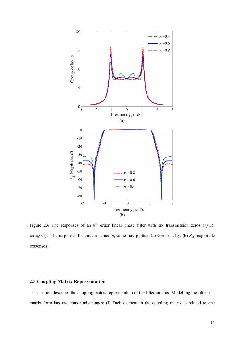
tuned/optimised by altering the real part of the transmission zeros (i.e. σ1), as shown in Figure 2.6. In
this figure, the linear phase filter has six transmission zeros at ±j1.5 and ±σ1±j0.4. The amplitude and
phase responses are plotted for three assumed σ1 values. As can be observed in Figure 2.6, for the
group delay response, there is another trade-off between the equalization bandwidth and the amplitude
of the group delay ripple over this bandwidth. The optimum locations of the complex transmission
zeros, which generate the desired/optimum group delay response, may be obtained through an
optimisation procedure. During the optimisation, both the real part and imaginary part of the complex
transmission zeros, are treated as control variables and altered at each iteration. This is described in
detail in [3].

13
(a)
(b)
(c)
Figure 2.5 Comparison of the amplitude and phase responses between the 8th order linear phase filter
(Case I) and the general Chebyshev filter (Case II). The six transmission zeros of the linear phase
filter are located at ±j1.5, ±0.6±j0.4. The general Chebyshev filter has two pure imaginary
transmission zeros positioned at ±j1.5.
-2 -1 0 1 2-100
-80
-60
-40
-20
0
Frequency, rad/s
S 21 m
agni
tude
, dB
Case ICase II
-2 -1 0 1 2-100
-80
-60
-40
-20
0
Frequency, rad/s
S 11 m
agni
tude
, dB
Case ICase II
-3 -2 -1 0 1 2 30
5
10
15
20
25
30
Frequency, rad/s
Gro
up d
elay
, s
Case ICase II
14
(a)
(b)
Figure 2.6 The responses of an 8th order linear phase filter with six transmission zeros (±j1.5,
±σ1±j0.4). The responses for three assumed σ1 values are plotted. (a) Group delay. (b) S21 magnitude
responses.
2.3 Coupling Matrix Representation
This section describes the coupling matrix representation of the filter circuits. Modelling the filter in a
matrix form has two major advantages: (i) Each element in the coupling matrix is related to one
-3 -2 -1 0 1 2 30
5
10
15
20
Frequency, rad/s
Gro
up d
elay
, s
1=0.4
1=0.6
1=0.8
-2 -1 0 1 2
-80
-70
-60
-50
-40
-30
-20
-10
0
Frequency, rad/s
S 21 M
agni
tude
, dB
1=0.8
1=0.6
1=0.4

15
physical element of the finished filter. This permits factoring in the effect of the electrical
characteristics (such as unloaded quality factor) of the physical filter. (ii) Matrix operations (such as
similarity transformation) can be performed on the original matrix to reconfigure the filter topology
[3]. These advantages are difficult to achieve for filters represented using polynomial transfer
functions.
Figure 2.7 Equivalent circuits of an n-coupled resonator filter. (a) The resonators are coupled by
mutual inductances (i.e. magnetic couplings). (b) The resonators are coupled by mutual capacitances
(i.e. electric couplings). [2]
Figure 2.7 (a) shows an equivalent circuit of an n-coupled resonator filter. In this figure, R, C, and L
stand for resistance, capacitance and inductance, respectively; i denote the loop current and es is the
voltage source. For this filter equivalent circuit, it is assumed that all the couplings are achieved via
mutual inductance between resonators. Kirchhoff’s voltage law (stating that the vector sum of all the
voltage drops around a loop is zero) is applied to the equivalent circuit shown in Figure 2.7 (a). This
leads to n equations, which can be expressed in a matrix form as, [2]

16
1 1 12 11
1
21 2 2 22
1 2
1
10
01
n
s
n
n
n n n nn
R j L j L j Lj C
i e
j L j L j L ij C
ij L j L R j L
j C
(2.11)
or
[ ]Z i e
where [Z] is an n × n impedance matrix. To simplify the problem, the filter is assumed to be
synchronously tuned, i.e. all the resonators are resonating at the same frequency ω0=1/(LC)0.5, where
L=L1=L2=…=Ln, C=C1=C2=….=Cn. Assuming a narrow-band approximation (i.e. ω≈ω0), the
normalised impedance matrix [ ]Z of the low-pass prototype filter can be expressed as [2]
12 11
21 2
1 2
1
[ ]
1
ne
n
n nen
p jm jmq
jm p jmZ
jm jm pq
where p is the complex lowpass frequency variable, qei is the normalised external quality factor and
mij is the normalised coupling coefficient between the ith and jth resonator. They can be obtained by [2]
0
0
0
1( )
1,
1
eii
ijij
p jFBW
Lq FBW for i n
R
Lm
L FBW
where FBW is the fraction bandwidth of the practical bandpass filter.

17
11 12 11
21 22 2
1 2
1
[ ]
1
ne
n
n n nnen
p jm jm jmq
jm p jm jmZ
jm jm p jmq
(2.12)
As stated in [2], to account for the asynchronously tuned filters, self-couplings (mii) can be added into
the entries on the main diagonal of the normalised impedance matrix, as shown in equation (2.12).
As mentioned before, the filter can also be represented using a network model as shown in Figure 2.1.
The S parameters of the filter equivalent circuit network can be obtained as [2]
121 1
1
111 11
1
12 [ ]
21 [ ]
ne en
e
S Zq q
S Zq
(2.13)
where [ ]Z is the normalised impedance matrix given in equation (2.12).
The equivalent circuit of the filter coupled by mutual capacitances, as shown in Figure 2.7 (b), can be
analyzed in a similar way. This is described in detail in [2]. The S parameters of the capacitance-
coupled filter network can be expressed as [2]
121 1
1
111 11
1
12 [ ]
2(1 [ ] )
ne en
e
S Yq q
S Yq
(2.14)
where [ ]Y is the normalised admittance matrix, given by [2]
18
11 12 11
21 22 2
1 2
1
[ ]
1
ne
n
n n nnen
p jm jm jmq
jm p jm jmY
jm jm p jmq
(2.15)
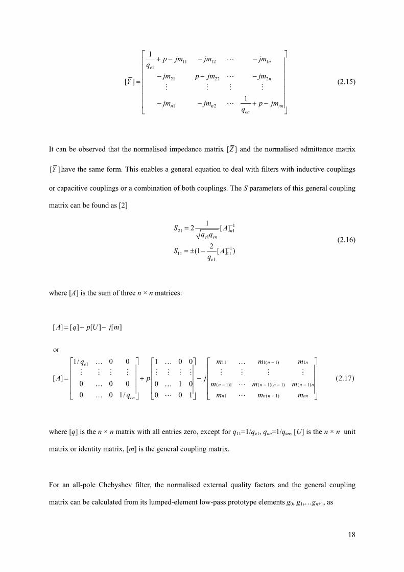
It can be observed that the normalised impedance matrix [ ]Z and the normalised admittance matrix
[ ]Y have the same form. This enables a general equation to deal with filters with inductive couplings
or capacitive couplings or a combination of both couplings. The S parameters of this general coupling
matrix can be found as [2]
121 1
1
111 11
1
12 [ ]
2(1 [ ] )
ne en
e
S Aq q
S Aq
(2.16)
where [A] is the sum of three n × n matrices:
11 1( 1) 11
( 1)1 ( 1)( 1) ( 1)
1 ( 1)
[ ] [ ] [ ] [ ]
or
1/ 0 0 1 0 0
[ ] (2.17)0 0 0 0 1 0
0 0 1/ 0 0 1
n ne
n n n n n
n n n nnen
A q p U j m
q m m m
A p jm m m
q m m m
where [q] is the n × n matrix with all entries zero, except for q11=1/qe1, qnn=1/qen, [U] is the n × n unit
matrix or identity matrix, [m] is the general coupling matrix.
For an all-pole Chebyshev filter, the normalised external quality factors and the general coupling
matrix can be calculated from its lumped-element low-pass prototype elements g0, g1,…gn+1, as

19
1 0 1eq g g 1en n nq g g , 1
1
1i i
i i
mg g
for i=1 to n-1 (2.18)
The low-pass g values for the all-pole Chebyshev filter are given by [2]
0
1
2 21
1 2
ln(coth( ))17.37
sinh( )2
1
2sin( )
2
(2 1) (2 3)4sin[ ] sin[ ]1 2 2 , 2,3,
( 1)sin [ ]
1 odd
coth ( ) even4
AR
ii
n
L
ng
gn
i in ng i n
ign
ng
n
(2.19)
The coupling matrices of other types of filters can be determined through an optimisation procedure.
This is discussed in depth in Chapter 6.

20
2.4 Physical Realization Using Waveguide Technology
2.4.1Rectangular waveguide
Figure 2.8 Geometry of a rectangular waveguide
A waveguide is one type of transmission line used to direct the propagation of microwave signals
along a predetermined path [4]. The rectangular waveguide is the most common type of waveguides
[4]. Figure 2.8 shows the geometry of a rectangular waveguide. Detailed introductions of the
waveguide theory are well covered in text books such as [1] and [4]. The following part presents a
few important properties of the rectangular waveguide.
It is well-known that TEM mode cannot be propagated inside a rectangular waveguide, since the
waveguide has only one conductor. Transverse electric (TE) and transverse magnetic (TM) modes are
supported by the rectangular waveguide. Each mode of the waveguide has a cut-off frequency, below
which propagation is not permitted [1]. The cut-off frequency associated with the TEmn or TMmn
mode can be found as [1]
2 21( ) ( )
2cmn
m nf
a b
(2.20)

21
where µ and ε are the permeability and the permittivity of the material filling inside the waveguide.
For typical rectangular waveguides (a = 2b), the TE10 mode is the dominant mode since it has the
lowest cut-off frequency. The second-lowest cut-off frequency corresponds to the TE20 mode. In the
majority of cases, the rectangular waveguide is operating in the band between the cut-off of the TE10
mode (i.e. fc10) and the cut-off of the TE20 mode (i.e. fc20=2 fc10). This ensures that only TE10 mode
propagates inside the waveguide. The useful bandwidth of this rectangular waveguide is fc20 - fc10 =
fc10.
It is worth mentioning that, if b ˃ a/2, the cut-off of the TE01 mode would become the second-lowest.
This reduces the useful bandwidth of the rectangular waveguide. Therefore, b is preferred to be no
bigger than a/2, in terms of the useful bandwidth. Conversely, the waveguide attenuation increases
with decreasing b [5]. If b˂ a/2, the attenuation would increase without improving the useful
bandwidth [5]. Therefore, the optimum b is exactly half of the broad sidewall dimension a.
According to the electromagnetic boundary conditions, the magnetic field (i.e. H field) is tangential to
the surface of the waveguide. The current flow in the walls can be derived by analysing H field, since
the current flow is perpendicular to the H field [4]. Figure 2.9 shows the wall currents for the TE10
mode in a rectangular waveguide. A general observation is that, no current flows across the centre line
of the broad sidewall. Splitting along this centre line would not seriously affect the waveguide wall
currents and the TE10 mode wave travelling underneath [4]. This is a useful conclusion for the layered
SU-8 micromachined waveguide circuits presented in Chapters 4 and 5.

22
Figure 2.9 The magnetic field lines and current density lines of a rectangular waveguide operating at
TE10 mode. In this figure, the red dotted line indicates the centre line of the broad face of the
waveguide. Conventionally the waveguide is split along this centre line since no current crosses it.
(This figure is reproduced from [5])
An ideal waveguide would transmit the microwave signal without loss of energy. However, for a
practical waveguide, attenuation can be caused by either dielectric loss or conductor loss. In this work,
dielectric loss is not taken into consideration since the waveguide is hollow. The attenuation due to
conductor loss for the waveguide operating at TE10 mode is given by [1]
2 3 23
(2 ) 8.686 dB/msc
Rb a k
a b k
(2.21)
where
0
2sR
k 2 2( )ka
(2.22)
Rs is the surface resistivity of the metallic walls, σ is the conducting wall conductivity, k is the wave-
number, ω is the angular frequency, β is the propagation constant for the TE10 mode and η is the
intrinsic impedance of the material filling in the waveguide.

23
2.4.2 Waveguide cavities
Figure 2.10 Geometry of a rectangular waveguide cavity.
Rectangular waveguide cavities are the basic building blocks of the waveguide filters. Figure 2.10
shows the geometry of a rectangular waveguide cavity resonator. A resonator has the ability to store
both electric energy and magnetic energy. Two important parameters of a resonator are: the resonant
frequency and the unloaded quality factor. The resonant frequency is the frequency at which the
stored electric energy equals the stored magnetic energy. The unloaded Q is used to characteristic the
inherent losses in a resonator [3]. A lower unloaded Q corresponds to a higher loss and vice versa. In
the following, the calculation of the resonant frequency and the unloaded Q, using the physical
dimensions of the waveguide resonator, is presented.
The transverse electric fields (Ex, Ey) of the TEmn or TMmn mode in the rectangular waveguide
resonator can be expressed as [1]
( , , ) ( , )[ ]mn mnj z j ztE x y z e x y A e A e (2.23)
where ( , )e x y represents the transverse variation of the mode, A+ and A- are arbitrary amplitude of the
forward and backward travelling waves [1]. βmn is the propagation constant for the TEmn or TMmn
mode and it can be found as

24
2 2 2( ) ( )mnm n
ka b
(2.24)
where k is the wave-number defined in equation (2.22). Appling the conditions that ( , ,0) 0tE x y and
( , , ) 0tE x y d to equation (2.23) leads to the following equation [1]:
1,2,3.....2g
mn
d l l for l
(2.25)
Equation (2.25) demonstrates that the length of the waveguide cavity d should be integer multiple of
the half guided wavelength (λg/2) of the considered mode at the resonant frequency [1]. Then the
modes existing in the waveguide resonator can be expressed as TEmnl or TMmnl , where m, n, l stands
for the number of modes in x, y, z directions, respectively [1]. The resonant frequency of the TEmnl or
TMmnl mode can be computed by [1]
2 2 2( ) ( ) ( )2
mnlr r
c m n lf
a b d
(2.26)
where µr and ɛr are the relative permeability and permittivity of the material filling the cavity, c is the
velocity of light in free space.
The unloaded quality factor of a waveguide resonator can be calculated as [1]
11 1( )u
c d
QQ Q
(2.27)
where Qc represents the loss caused by lossy conducting walls, whereas Qd is used to factor in the loss
of the dielectric filling in the cavity. In this work, the material filling the waveguide cavity is air,

25
therefore, only Qc is considered here for the calculation of the unloaded quality factor. The Qc of a
waveguide resonator operating at the TE10l mode is given by [1]
3
2 2 3 3 2 3 3
( ) 1
2 (2 2 )cs
kad bQ
R l a b bd l a d ad
(2.28)
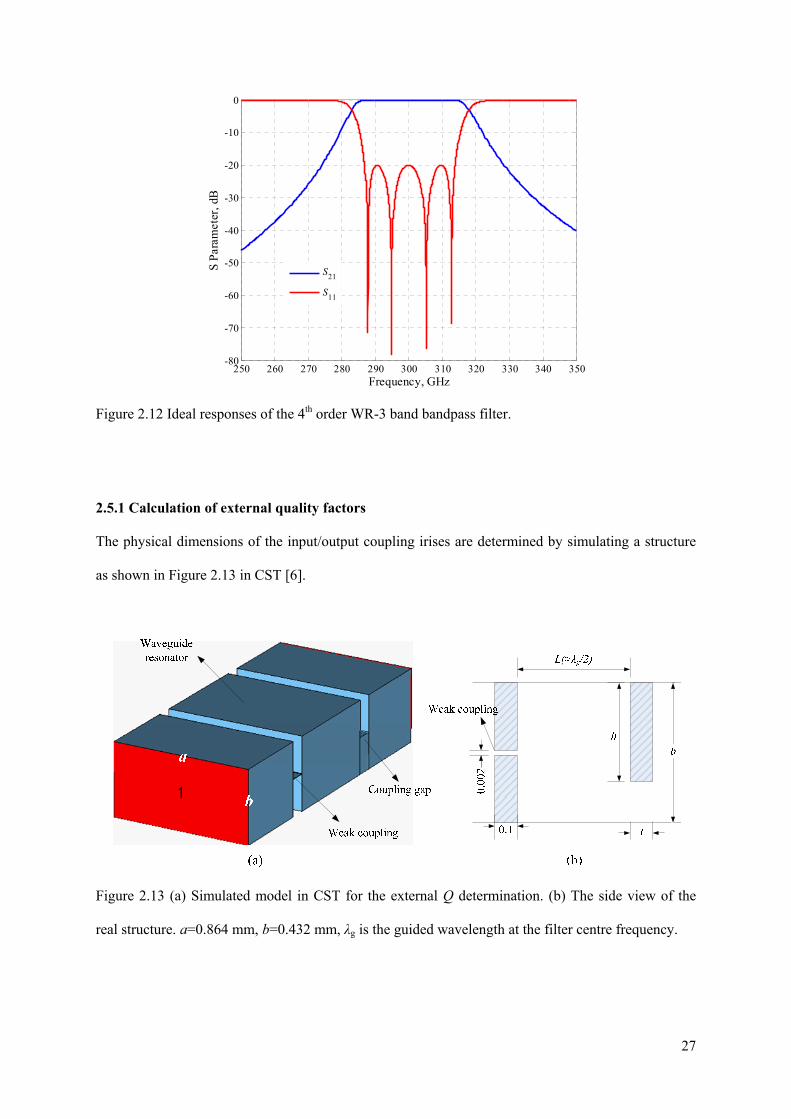
2.5 Design of Iris Coupled Waveguide Resonator Filters
From the filter’s specifications, the input/output couplings (i.e. external quality factors) and the inter-
resonator coupling coefficients can be obtained. Then the physical dimensions of the filter are able to
be extracted from these coupling coefficients. In the following, the design of a 4th order Chebyshev
WR-3 band waveguide resonator filter is presented as an example. The filter structure is shown in
Figure 2.11. It consists of four waveguide resonators operating in the TE101 mode. Both the internal-
resonator-couplings and the input/output couplings are realized using asymmetrical capacitive irises.
Figure 2.11 The structure of the 4th order waveguide resonator filter. The blue part is vacuum, which
is surrounded by perfect electric conductor (PEC) in the simulation.

26
The specifications of this filter are:
Filter order: n=4
Centre frequency: f0 = 300 GHz
Fractional bandwidth (FBW): 9%
Passband ripple: LAR= 0.0436 dB (equivalent to a passband return loss of 20 dB).
Applying equation (2.19), the g values for the 4th order Chebyshev lowpass prototype filter with a 20
dB return loss can be calculated as g0= 1, g1 =0.9314, g2 =1.292, g3 =1.5775, g4 =0.7628 and g5 =1.221.
Substituting these g values into equation (2.18), the normalised external quality factors and the
coupling coefficients could be determined as qe1=qe4=0.9314, m12=m34=0.9116, m23=0.7005.
The external quality factors and the coupling coefficients of the practical bandpass filter, and the
normalised coupling coefficients of the low-pass prototype filter, are related via the following
equation [2]
11
eeq
QFBW
enenq
QFBW
, 1 , 1i i i iM FBW m for i=1 to n-1 (2.29)
Table-2.1 lists the calculated external quality factors and coupling coefficients of the WR-3 band
bandpass filter.
Table-2.1 Required coupling coefficients and external quality factors for the
fourth order Chebyshev filter
n=4 Passband ripple Qext M12 M23 M34
0.0436 dB 10.3489 0.0820 0.0630 0.0820
Figure 2.12 shows the ideal response of the bandpass filter plotted using the coupling matrix elements
listed in Table-2.1.
27
Figure 2.12 Ideal responses of the 4th order WR-3 band bandpass filter.
2.5.1 Calculation of external quality factors
The physical dimensions of the input/output coupling irises are determined by simulating a structure
as shown in Figure 2.13 in CST [6].
Figure 2.13 (a) Simulated model in CST for the external Q determination. (b) The side view of the
real structure. a=0.864 mm, b=0.432 mm, λg is the guided wavelength at the filter centre frequency.
250 260 270 280 290 300 310 320 330 340 350-80
-70
-60
-50
-40
-30
-20
-10
0
Frequency, GHz
S P
aram
eter
, dB
S21
S11

28
Figure 2.14 Simulation results of the structure shown in Figure 2.13.
Figure 2.14 shows the simulation results of the structure given in Figure 2.13. From the simulation
results, the external quality factor can be calculated directly from the resonant frequency (fo) and the 3
dB bandwidth ( ∆f ), as stated below:
oext
fQ
f
(2.30)
The resonant frequency of the simulated structure varies with the length of the waveguide resonator
(L). L should be adjusted to ensure that the simulated model is resonating at the filter’s centre
frequency. The required external Q can be achieved by altering the height of the coupling iris (h) and
the thickness of the coupling iris (t). For this filter, the thickness of all the irises (t) is selected as 0.1
mm, and the height of coupling iris (h) is varied to provide the required coupling coefficient. To
employ equation (2.30) for the external Q calculation, the coupling from the feed waveguide on the
left side must be very weak.
f0
∆f
3 dB

29
As the height of the coupling iris h increases, the external Q increases and the resonant frequency fo
decreases. This means that the resonant frequency fo is not only determined by the resonator length L
but also the iris height h. Thus, in the presence of the fixed iris thickness t, both h and L should be
adjusted to achieve the desired external Q and the resonant frequency fo. h=0.187 mm and L=0.674
mm are selected as the initial dimensions for the final filter design, since Qext and fo values produced
by this set of parameter values are the closest to that required.
2.5.2 Calculation of inter-resonator couplings
The external Q characterizes the external coupling between the filter and the external circuit. The
relationship between the inner resonators is expressed by the coupling coefficient between them. In
[2], the coupling coefficient of two resonators is defined as the ratio of coupled energy to stored
energy, which can be expressed as
1 2 1 2
2 2 2 21 2 1 2| | | | | | | |
E E d H H dkc
E d E d H d H d
(2.31)
where E
and H
represent the electric and magnetic field vectors, respectively, as shown in Figure
2.15. The first term on the right side of the equation represents the electric coupling and the second
term indicates the magnetic coupling. The mixed coupling results from the superposition of the
magnetic and electric couplings.
Figure 2.15 An illustration of two coupled resonators. (This figure is reproduced from [2])

30
The electric wall and magnetic wall symmetry can be used for the inter-resonator coupling calculation.
This calculation method works by dividing two coupled resonators into two single resonators
terminated by a magnetic wall and an electric wall [2]. The coupling is then determined from the
knowledge of the resonant frequencies of two individual resonators. However, this calculation method
is experimentally difficult to implement. An alternative method to calculate the coupling coefficient is
to simulate a structure as shown in Figure 2.16. The ports need to be weakly coupled to resonators for
this approach to work. A sketch of |S21| is given in Figure 2.17. The split resonant frequency can be
observed from the two peaks of |S21| and the nature of the coupling (electric or magnetic) can be
determined from the phase information of S21 [2]. 0.
002
0.00
2
Figure 2.16 The two-coupled waveguide resonator structure. (a) The simulated model in CST. (b) An
illustration of the real structure. a=0.864 mm, b=0.432 mm, λg is the guided wavelength at the filter
centre frequency.
Figure 2.17 Typical S21 (in dB) resonant response of two coupled resonators as shown in Figure 2.16.
The frequencies of two resonant peaks are f1 and f2.
250 260 270 280 290 300 310 320 330
-70
-60
-50
-40
-30
-20
-10
Frequency, GHz
|S21
| , d
B
f2 f1

31
The relationship between the coupling coefficient ( kc ) and the resonant frequencies (f1, f2) is given by
2 2
2 12 2
2 1
f fkc
f f
(2.32)
For the simulated structure, the length of two resonators (L) is roughly λ/2. The thickness of the iris
thickness t is 0.1 mm. The coupling coefficients can be controlled by varying the height of the
coupling iris h. Basically, an increase of the coupling iris height h leads to a reduction of the coupling
coefficient, when the thickness of the coupling iris t is fixed. The middle frequency of these two
resonant peaks (i.e. (f1+f2)/2) also varies with h. For synchronous tuned filter, where all the resonators
have the same resonant frequency, the middle frequency of these two peaks should in accordance with
the filter centre frequency fo.
The corresponding iris heights for the required coupling coefficients (i.e. M12, M23, M34), are obtained
as h12= h34=0.308 mm and h23=0.326 mm.
2.5.3 Final optimisation
After obtaining the initial parameter values for the filter design, four resonators are in series
connection to establish the bandpass filter. The simulation responses for the first attempt shown as
before optimization can be observed from Figure 2.18. The initial results are in reasonable agreement
with the specifications. Further CST optimizations are carried out to shift the filter centre frequency to
300 GHz and reduce the return loss in the passband to the specified 20 dB. During the optimisation,
the lengths of the four resonators and the heights of the coupling irises have been adjusted. The S
parameter response after optimisation is displayed in Figure 2.18. Its associated physical dimensions
are given in Figure 2.19. This filter has been fabricated using the SU-8 micromachining process. The
measurement results of this filter are presented in Chapter 4.

32
Figure 2.18 CST simulated performance of the designed WR-3 band fourth order filter.
Figure 2.19 A schematic side-view diagram of the 4th order iris coupled WR-3 filter, drawing is not to
scale. Some critical dimensions of the filter: h1=0.170 mm, h2= 0.284 mm, h3=0.318 mm, L1=0.706
mm, L2=0.664 mm, t = 0.1 mm, b=0.432 mm.
250 260 270 280 290 300 310 320 330
-60
-50
-40
-30
-20
-10
0
Frequency, GHz
S P
aram
eter
, dB
S11
(Before Optimisation)
S21
(Before Optimisation)
S11
(After Optimisation)
S21
(After Optimisation)
33
2.6 Conclusions
The fundamental theory of coupled resonator filters is explained in this chapter. It begins with
describing the transfer function polynomial synthesis process for some classical prototype filters: all-
pole Chebyshev filters, general Cheyshev filters and linear phase filters. Then the coupling matrix
representation of a resonator-coupled filter is introduced. This is followed by a discussion of
implementation of the filter resonators using rectangular waveguide cavities. In the final part of this
chapter, the design and physical realization of an iris coupled waveguide filter is presented as an
example.
Reference
[1] Pozar D. M.: ‘Microwave Engineering’ (Third edition, John Wiley & Sons, Inc, 2005).
[2] Hong Jia-Sheng, Lancaster Mike J. ‘Microstrip Filters for RF/Microwave Applications’ (Wiley &
Sons Inc., 2001).
[3] Cameron R.J., Kudsia C.M., Mansour R.R. ‘Microwave Filters for Communication Systems
Fundamentals, Design and Applications’ (Jon Wiley & Sons, Inc. 2007).
[4] Cronin N.J.: ‘Microwave and Optical Waveguides,’ (Iop Publishing Ltd, 1995)
[5] Sorrentino R., Bianchi G. ‘Microwave and RF Engineering,’ (John Wiley and Sons, 2010)
[6] CST Microwave Studio, CST GmbH, Darmstadt, Germany, 2006
34
Chapter 3
Micromachining
Terahertz radiations are the electromagnetic waves with a frequency range from about 0.1 THz (i.e.
100 GHz) to 10 THz, which lie between the microwave and infrared regions of the spectrum.
According to majority of textbooks, in this terahertz band, the frequency range between 300 GHz to 3
THz is also well-known as the submillimeter wave spectrum, whereas the frequency range between 30
GHz to 300 GHz is referred to as millimetre waves. Recently the terahertz spectrum has been
attracting more and more attention due to its promising applications such as medical imaging, security
scanning and communications in space or high-altitude earth atmosphere. These are described in
detail in Section 3.1.
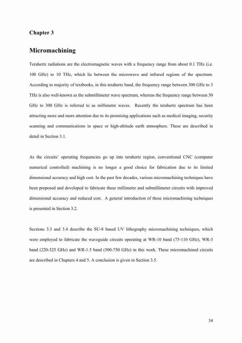
As the circuits’ operating frequencies go up into terahertz region, conventional CNC (computer
numerical controlled) machining is no longer a good choice for fabrication due to its limited
dimensional accuracy and high cost. In the past few decades, various micromachining techniques have
been proposed and developed to fabricate these millimetre and submillimeter circuits with improved
dimensional accuracy and reduced cost. A general introduction of these micromachining techniques
is presented in Section 3.2.
Sections 3.3 and 3.4 describe the SU-8 based UV lithography micromachining techniques, which
were employed to fabricate the waveguide circuits operating at WR-10 band (75-110 GHz), WR-3
band (220-325 GHz) and WR-1.5 band (500-750 GHz) in this work. These micromachined circuits
are described in Chapters 4 and 5. A conclusion is given in Section 3.5.

35
3.1 Terahertz Applications
Terahertz radiation has three primary properties for applications: (i) it is able to pass through
dielectrics such as paper, plastic, cloth, wood, ceramics and silicon, which are also common packing
materials, with little attenuation; (ii) metals are highly reflective in the terahertz region due to the
short penetration depth; (iii) many substances, including chemical and biological agents, have unique
spectral fingerprints in the terahertz frequency region [1]. These properties make it ideally suitable for
many imaging applications like non-destructive testing to inspect sealed packages such as mail
envelops and luggage and personal belongings in the airport and train stations [1-2]. Figure 3.1 shows
a terahertz image of a sealed box, which contains several metal and plastic objects. As can be seen,
the contents inside the box can be clearly identified from the terahertz image. The metallic objects are
opaque in the image because they completely block the terahertz radiation.
Figure 3.1 Terahertz image of a closed 80 mm long cardboard box. This box contains several objects
as indicated in the figure. (This figure is reproduced from [2].)
Compared with X-rays, terahertz radiations have one major advantage that they do not present health
hazard to people being scanned or to people operating the scanned systems. The risk brought by X-
rays is attributed to the high energy carried by each X-ray photon [2]. Typically, X-ray photon energy
is in the range of keV, which is sufficient to create ionization in biological tissue [2-3]. Terahertz
A polyethylene washer
A 10 mm thick rubber eraser
A metallic paper clip
A metal washer
A key
A metal pin with a polystyrene handle
A metal nut

36
photon energy is weaker by about six orders of magnitude (for instance, 4 meV at 1 THz) [2-3]. That
is believed to have negligible effect on living tissue [2]. As mentioned before, typical wrapping and
packing materials like cloth are transparent to terahertz radiation, whereas plastic and ceramic guns,
liquid explosives and drugs can be distinguished by terahertz imaging from their unique spectral
fingerprints. Therefore, terahertz imaging systems are also ideal approaches for passengers’ body
scans at airports for detection of concealed weapons and explosives under layers of cloth without
physical contact [1]. Figure 3.2 shows terahertz images for the concealed weapons detection purposes,
in which the threat objects have been clearly revealed and identified. Passive images are formed by
gathering the natural radiation from objects and then producing the images by means of contrasts
between thermally warmer and colder objects and also the differences in material emissivity. An
active imaging system works more like radar. It illuminates the scene with a beam of terahertz wave
and subsequently records the reflected energy within the system’s field of view [4]. Active imaging
systems could be operated at extremely low power level, which does not present health hazard to the
people under inspection [4].
(a) (b)
Figure 3.2 Active and passive terahertz images. (a) A passive image obtained at 94-GHz, a metal
knife is hidden inside a newspaper and is exposed in the image. (b) A 640 GHz active image, which
exhibits a toy gun under cotton shirt. (This figure is reproduced from [5].)

37
Figure 3.3 Terahertz images of some tissue samples. A liver cancer sample at (a) 567 GHz and (b)
676 GHz, the arrows denote cancer areas. (c) A breast cancer sample, the dotted line indicates the
cancer areas. (This figure is reproduced from [2].)
Apart from above security applications, terahertz radiation has also been widely applied for medical
imaging due to its properties such as (i) non-ionising; (ii) low operating power level; (iii) high signal
to noise ratio; (iv) wavelength longer than optical radiation, which can offer a good resolution as well
as smaller scattering in biological tissue; (v) high sensitivity to the water content in biological tissues
[6]. Most applications of terahertz radiation in the medical field are focusing on imaging epithelial
tissue, because of the strong water absorption in the terahertz region [6]. This will not limit the
applications of terahertz medical imaging, since epithelial or surface tissues contribute more than 80%
of all adult cancers including common cancers of skin, lung and liver and so on [6]. Figure 3.3
illustrates the terahertz images of some excised tissue cancer samples, in which the brightness and
texture of cancer part are different from the rest of the sample.

38
For communications systems, higher frequency carriers enable larger available bandwidth.
Additionally, the use of higher frequencies will lead to reduced dimensions of the components, since
the circuit dimensions and its operating wavelength should be of the same order of magnitude. These
should be major advantages of terahertz communication systems. However, in practice a terahertz
wave cannot travel long distances in earth’s atmosphere due to the large atmospheric attenuation and
attenuation from atmospheric particulates (i.e. rain, fog and dust, etc). Figure 3.4 illustrates the
atmospheric attenuation at frequencies from 100 GHz to 1 terahertz for six different atmospheric
conditions, all at the sea level. As can be seen in the figure, the attenuation increases rapidly as the
frequency increases. At frequencies over 400 GHz, the peak attenuation is in excess of 1 dB/m. This
high attenuation prevents the use of terahertz wave in long distance communication systems. In space
or high-altitude in the earth’s atmosphere, above altitudes where water and other atmospheric
particulates bring serious signal absorption, there is a promising future for applications of terahertz
waves in communication systems.
Figure 3.4 Calculated atmospheric attenuation as a function of frequency for a few different
atmospheric conditions at sea level pressures. (This figure is reproduced from [5].)
39
Due to the intense impact of atmospheric attenuation on the terahertz wave propagation, it is
suggested that the terahertz devices/systems should operate below 400 GHz or at propagation
windows where minimum attenuation occurs such as 340 GHz, 650 GHz, 850 GHz, 1.05 THz and 1.5
THz [4]. In this work, several waveguide devices working at 100 GHz, 300 GHz and 650 GHz, have
been designed and fabricated using the SU-8 micromachining techniques, and measured.
3.2 Terahertz Waveguide Circuits
The fabrication of microwave circuits at terahertz frequencies using traditional methods, such as metal
milling or electrical discharge machining, can be very expensive and usually suffers from a lack of
dimensional accuracy. In recent years, several different micromachining technologies have been
developed as potential fabrication technique alternatives, such as silicon deep reactive ion etching
(DRIE), LIGA processing, or laser machining. The following subsections present a general
introduction of these different fabrication techniques.
3.2.1 Conventional machining
Traditionally, geometrically simple millimetre wave devices are fabricated by milling on a high
precision Computer Numerical Control (CNC) machine. Recently, this end-mill machining technique
has been further developed and applied to fabricate several terahertz waveguide circuits operating at
frequencies up to 1.5 THz, with a very high dimension accuracy (i.e. typically within 2-3 µm of the
designed values), as reported by Jet Propulsion Laboratory (JPL) at California, USA in [7]. They also
claimed the capacity of cutting 15 µm wide channels on a solid metal block using end mills. Two
terahertz waveguide circuits, fabricated using this high precision end-mill machining technique by the
JPL, are exhibited in Figure 3.5. Although the metal milling method is still capable of fabricating
terahertz waveguide components with high dimensional precision, its wide usage has been precluded
by a few drawbacks, as listed in the following: (i) the unit cost will increase dramatically as the
feature sizes decrease (i.e. frequency increases) [8]; (ii) for narrow trenches (smaller than 1 mm wide),

40
the length of the milling cutter has to be small to fulfil the strength requirement. This limits the typical
achievable maximum aspect ratio (i.e. the ratio of the dimension in depth to that of the surface) of the
trenches in a range of 2~3:1 [9]; (iii) round internal corners exist due to the limited diameter (>150
µm) of the cutter; (iv) it is not suitable for large scale production because it is a serial processing
method.
(a) (b)
Figure 3.5 State-of-art CNC machined terahertz devices. (a) A four-chip frquency tripler operating at
260-340 GHz band. (b) A 1.5 THz Hot-Electron Bolometer (HEB) mixer with integrated feed horn.
(This figure is reproduced from [7].)
3.2.2 Micromachining
Apart from conventional machining, a wide range of micromachining techniques have been proposed
recently and developed to fulfil the need of terahertz waveguide circuits with complex geometries,
high dimension accuracy, low cost and the capacity for large scale production. These micromachining
techniques can be broadly categorized into four groups: bulk micromachining, surface
micromachining, LIGA process and laser machining.
3.2.2.1 Bulk micromachining
A device fabricated by bulk micromachining is formed by selectively removing (i.e. etching) the
materials from the bulk substrate, which is normally a silicon wafer. Bulk micromachining can be

41
classified into two groups by the types of etching methods: wet etching and dry etching. Wet etching,
in which chemical etchants are used to etch a protective mask covered substrate, is relatively cheap
and simple, but it is difficult to control the etch rate and critical dimensions [10]. In wet etching
processes, undercutting effects should be considered for isotropic substrates (i.e. uniform etch rate in
all directions), whereas anisotropic etching (i.e. crystal orientation dependant etch rates) is limited by
the crystal orientations of silicon wafers (i.e. <100>, <110> and <111> plane) [11]. This is shown in
Figure 3.6. This wet etching technique has been applied to fabricate various terahertz circuits
including a W-band waveguide [12] and two W-band filters [13].
Figure 3.6 Bulk silicon micromachining technique wet etching methods. (a) isotropic wet etching. (b)
anisotropic etching on silicon wafer with <100> crystal orientation. (c) anisotropic etching on silicon
wafer with <110> crystal orientation.(Drawings are not to scale). [26]

42
Dry etching employs gaseous etchants rather than liquids to remove the unwanted substrate materials.
Three dry etching techniques are available: plasma, ion milling and reactive ion etching (RIE) [10].
Among them, the deep reactive ion etching (DRIE) technique, which combines the physical and
chemical etching process, has drawn the most attention due to its capacity of producing structures
with arbitrarily defined features [14], high maximum aspect ratio(>30:1) [10], excellent critical
dimension control [10] and virtually vertical walls [10]. An illustration of the key steps of DRIE
process is given in Figure 3.7. The process starts from depositing silicon oxide (i.e. SiO2) on both side
of the substrate wafer. Then photoresist is applied on top of the SiO2 layer. After patterning and
developing the photoresist layer, the exposed SiO2 layer is etched to form the oxide mask. Then the
photoresist layer is removed and the silicon substrate is etched. Finally both the top and bottom SiO2
layers are removed by buffered oxide etch (BOE) solution. The resulting silicon layer is coated with
Ti layer and Cu layer.
DRIE has been used for the fabrication of many terahertz waveguide circuits for instance a 600 GHz
branch-line coupler [14], a 900 GHz frequency tripler [8] and a W-band hybrid coupler and power
divider [15].
The major drawbacks of bulk micromachining are that: (i) the height of structure is limited by
commercially available silicon wafer thickness [10]; (ii) there is difficulty in high aspect ratio
sidewall metallization [14].

43
Figure 3.7 Key steps of DRIE fabrication process. The top SiO2 layer is utilized as the DRIE mask,
whereas the bottom SiO2 layer is the stop layer for the etching. [27]
3.2.2.2 Surface micromachining
Unlike bulk micromachining, which is based on selectively etching the substrate using physical or
chemical means, surface micromachining builds the structures on top of the substrate wafer. Therefore,
surface micromachining structures can achieve a wide range of desired thicknesses. Figure 3.8
illustrates the typical fabrication steps of the surface micromachining process. The thin films on top
of the substrate (typically silicon) are patterned by photolithography and the unwanted regions are
selectively removed by etching. The sacrificial layer, as shown in Figure 3.8, is introduced for
temporary support of the structure layer during fabrication and is removed at the very end of the
fabrication process. Apart from SiO2, other materials such as metals, polymers and polyimides can

44
also be chosen as sacrificial layers [4]. Surface micromachining could also be carried out using a dry
etching process.
Surface micromachining is more expensive than the bulk micromachining, however, it offers a few
advantages over bulk micromachining: (i) a wide range of materials can be utilized in the layer
structure building; (ii) the structure thickness is not constrained by the thickness of silicon substrate
wafers; (iii) complex geometries can be obtained using surface micromachining [10].
Surface micromachining has been employed to produce a large variety of terahertz waveguide
components including a W-band (i.e. 75-110 GHz) straight through waveguide [29], three V-band (i.e.
50-75 GHz) air cavity filters [30].

45
Figure 3.8 Typical steps of surface micromachining process. [26]
46
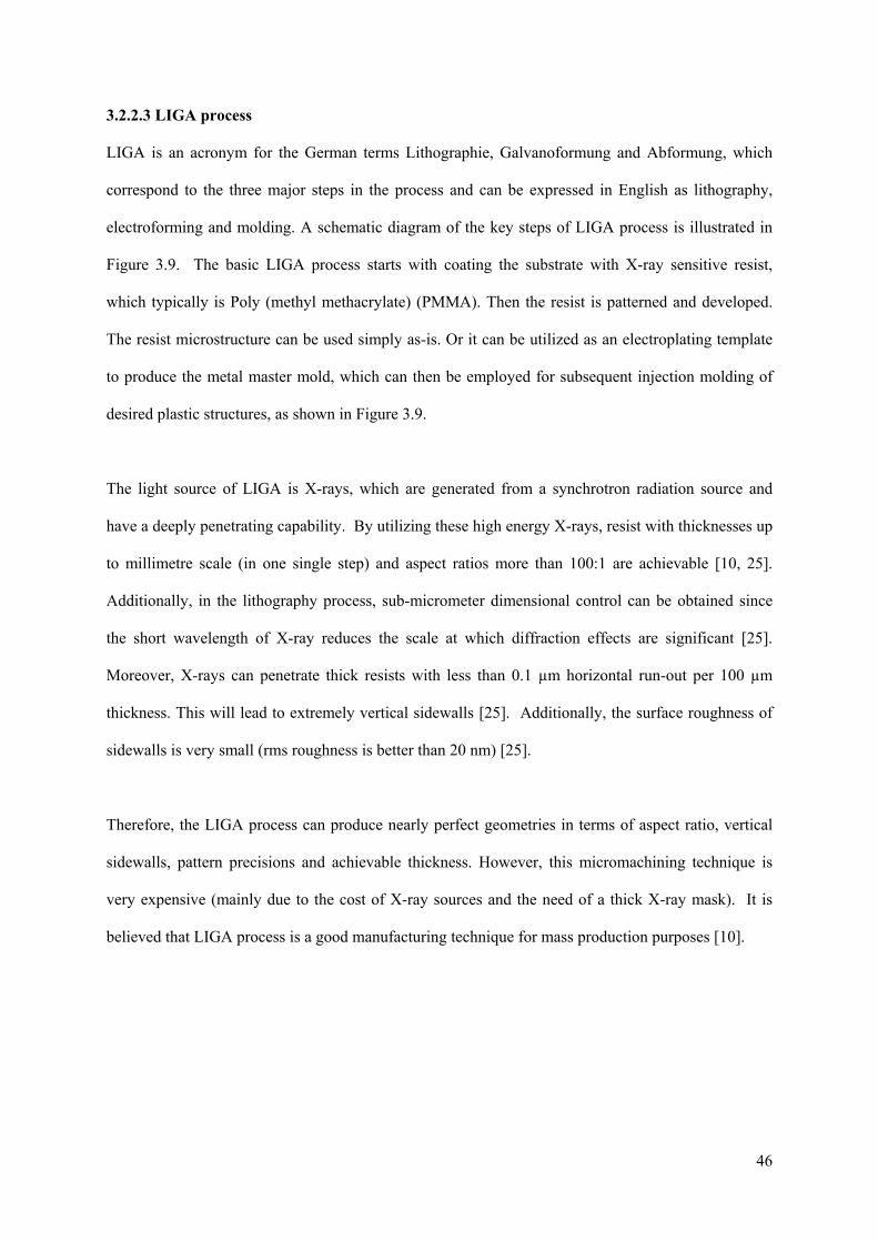
3.2.2.3 LIGA process
LIGA is an acronym for the German terms Lithographie, Galvanoformung and Abformung, which
correspond to the three major steps in the process and can be expressed in English as lithography,
electroforming and molding. A schematic diagram of the key steps of LIGA process is illustrated in
Figure 3.9. The basic LIGA process starts with coating the substrate with X-ray sensitive resist,
which typically is Poly (methyl methacrylate) (PMMA). Then the resist is patterned and developed.
The resist microstructure can be used simply as-is. Or it can be utilized as an electroplating template
to produce the metal master mold, which can then be employed for subsequent injection molding of
desired plastic structures, as shown in Figure 3.9.
The light source of LIGA is X-rays, which are generated from a synchrotron radiation source and
have a deeply penetrating capability. By utilizing these high energy X-rays, resist with thicknesses up
to millimetre scale (in one single step) and aspect ratios more than 100:1 are achievable [10, 25].
Additionally, in the lithography process, sub-micrometer dimensional control can be obtained since
the short wavelength of X-ray reduces the scale at which diffraction effects are significant [25].
Moreover, X-rays can penetrate thick resists with less than 0.1 µm horizontal run-out per 100 µm
thickness. This will lead to extremely vertical sidewalls [25]. Additionally, the surface roughness of
sidewalls is very small (rms roughness is better than 20 nm) [25].
Therefore, the LIGA process can produce nearly perfect geometries in terms of aspect ratio, vertical
sidewalls, pattern precisions and achievable thickness. However, this micromachining technique is
very expensive (mainly due to the cost of X-ray sources and the need of a thick X-ray mask). It is
believed that LIGA process is a good manufacturing technique for mass production purposes [10].

47
Figure 3.9 Some key steps of LIGA process. The last two steps can be repeated for mass production.
[20]

48
3.2.2.4 Laser machining
Laser light, with high power density and very low angle divergence, has also been employed for
micromachining. Laser light is capable of producing micromachined photoresists with almost vertical
sidewalls and high aspect ratios. Three types of lasers, carbon dioxide (CO2) lasers, neodymium
YAG (Nd:YAG) lasers and excimer lasers, are specially suitable for micromachining purposes [20].
The first two lasers are infrared (IR) lasers, which make use of localized heating by a laser beam spot.
IR lasers can be applied for three brief micromachining applications: drilling and cutting, welding, or
heat treatment [20]. The major drawback of IR lasers is that the material adjacent to the machined
area will be affected by the heat.
Excimer lasers produce short pulses in the ultraviolet range. They have been employed to fabricate
industrial components with feature size ranges between 0.05 to 1000 µm successfully [24]. The
selective removal of material is a result of interaction between the excimer laser light and chemical
bonds within the material [20], in other words the individual molecules of the material are heated to
transfer the material from solid state to gas state. Normally a mask similar to that used for
photolithography is employed to define the patterns of the structures, as shown in Figure 3.10. The
depth of cutting by excimer laser can be controlled accurately via the number of pulses, and a depth of
hundreds of microns is achievable [20]. Both vertical sidewalls and tapered sidewalls (by adjusting
the incident angle of laser light) can be obtained. This excimer laser micromachining technique is
typically adopted for polymer materials. It can also be applied to deal with ceramics, and metal layers
if laser power densities are sufficient.
Note that, excimer laser can also be utilized for precision drilling process [24]. Figure 3.11 shows
two micromachined structures made by excimer laser drilling and excimer laser ablation, respectively.

49
Figure 3.10 Illustration of the excimer laser ablation by utilising an imaging mask. Both the mask and
the CNC chuck can be moved to produce large structures with complex patterns. An optical
demagnification can be applied to increase the laser energy density on the machined material surface.
[20]
Figure 3.11 Excimer laser micromachined structures. (a) Pyramids obtained using mask-dragging
technique. (b) laser-drilled ink jet printer non-linear tapered nozzles. (This figure is reproduced from
[24])

50
3.3 Separate SU-8 Single-Layer Fabrication Process
SU-8 is a negative epoxy-based photoresist invented by IBM-Watson Research Centre in 1989 [10].
It can be applied to build photoresists with thickness from 1 µm to 2 mm [16], and structures with
high aspect ratio (>15:1) [9]. SU-8 resist is ultraviolet (UV) light sensitive, which enables the
utilization of the relatively cheaper UV-lithography process. These superior properties of SU-8 make
it a popular choice as a micromachining material. In this work, two different SU-8 UV-lithography
processes are used: a separate SU-8 single-layer process and a fully jointed SU-8 two-layer process.
In the following sections, the separate SU-8 layer fabrication process will be presented. The fully
jointed SU-8 two-layer fabrication process will be described in Section 3.4.
3.3.1 General SU-8 fabrication process
SU-8 photoresist waveguide circuits can be constructed using the following process steps: spin coat,
soft bake, exposure under UV light, post exposure bake, development, hard bake and substrate
removal, metallization and bonding. This is illustrated in Figure 3.12 and the process used for the
circuits presented in this thesis is described in detail below.

51
Figure 3.12 Key steps of the separate SU-8 single-layer micromachining technique fabrication process.
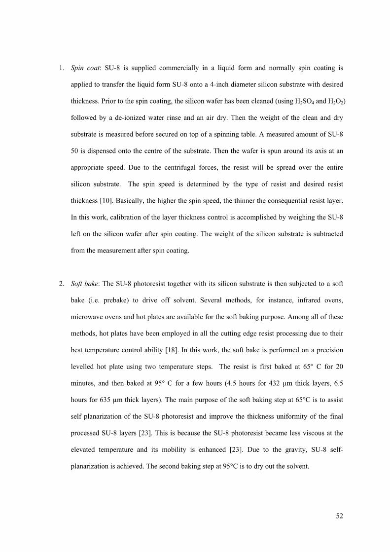
52
1. Spin coat: SU-8 is supplied commercially in a liquid form and normally spin coating is
applied to transfer the liquid form SU-8 onto a 4-inch diameter silicon substrate with desired
thickness. Prior to the spin coating, the silicon wafer has been cleaned (using H2SO4 and H2O2)
followed by a de-ionized water rinse and an air dry. Then the weight of the clean and dry
substrate is measured before secured on top of a spinning table. A measured amount of SU-8
50 is dispensed onto the centre of the substrate. Then the wafer is spun around its axis at an
appropriate speed. Due to the centrifugal forces, the resist will be spread over the entire
silicon substrate. The spin speed is determined by the type of resist and desired resist
thickness [10]. Basically, the higher the spin speed, the thinner the consequential resist layer.
In this work, calibration of the layer thickness control is accomplished by weighing the SU-8
left on the silicon wafer after spin coating. The weight of the silicon substrate is subtracted
from the measurement after spin coating.
2. Soft bake: The SU-8 photoresist together with its silicon substrate is then subjected to a soft
bake (i.e. prebake) to drive off solvent. Several methods, for instance, infrared ovens,
microwave ovens and hot plates are available for the soft baking purpose. Among all of these
methods, hot plates have been employed in all the cutting edge resist processing due to their
best temperature control ability [18]. In this work, the soft bake is performed on a precision
levelled hot plate using two temperature steps. The resist is first baked at 65° C for 20
minutes, and then baked at 95° C for a few hours (4.5 hours for 432 µm thick layers, 6.5
hours for 635 µm thick layers). The main purpose of the soft baking step at 65°C is to assist
self planarization of the SU-8 photoresist and improve the thickness uniformity of the final
processed SU-8 layers [23]. This is because the SU-8 photoresist became less viscous at the
elevated temperature and its mobility is enhanced [23]. Due to the gravity, SU-8 self-
planarization is achieved. The second baking step at 95°C is to dry out the solvent.

53
3. Exposure to UV light: The SU-8 resist is then exposed under UV light to define patterns of the
waveguide layer by means of a mask. The mask is basically a piece of glass covered by
chromium. The chromium at the parts corresponding to the pattern of waveguide circuit is
removed. By projecting UV light onto the mask, the pattern is transformed from mask to the
photoresist, since chromium is opaque to UV light, whereas glass is transparent. The
solubility of the resist changes when it is exposed under UV light [10]. The exposure time
depends on the exposure energy required by the supplied SU-8. Additionally, SU-8 has a low
UV absorption property. This enables multiple exposures for thick SU-8 resist, which leads to
a full exposure at the bottom part of the resist. The structural dimensions in SU-8 achieved by
the photolithography process are associated with the chosen wavelength of the UV light [20].
This is because diffraction will occur when light is incident upon a small aperture, and this
diffraction effect will become considerable in the case where the structure dimensions are
comparable with the wavelength of light [10]. Exposure of the photoresist is carried out by
placing the wafer with the resist under a mercury lamp UV sources from a Canon PLA-510
mask aligner. Initially signals with wavelength under 400 nm is filtered out by a L39 optical
filter, so the resist is exposed with h line (405 nm) in order to penetrate effectively through
the thick resist. Multiple exposure steps (i.e. expose 40 seconds and repeat for five times) are
used in order to reduce surface heat between the mask and the resist. It is widely known that h
line (405 nm) and g line (436 nm) can penetrate into SU-8 resist with bigger depth than i line
(365 nm), however, i line is more effective in terms of generating acid for cross linking
purpose [23]. Therefore, the main i line (365 nm) signal is then utilized to expose the SU-8
photoresist for 3 times 40 seconds in order to make sure sufficient acid is generated for cross-
linking purpose. This is accompanied by filtering out signals with wavelength under 360 nm
through an optical PL360 filter. Those short wavelength signals are harmful here because they
generate most of the surface heat.
4. Post exposure bake: A post exposure bake process, which is normally required by negative
resists, is used to produce the cross-linking reactions [20]. These cross-linked regions will be

54
insoluble in the developer. It should be noted that cracking of SU-8 often occurs after the post
exposure bake. The control of temperature of the post exposure bake process should be
precise, to minimise the internal tensile stress which result in cracks. In this work, the post
exposure bake is carried out on a hot plate at 65° C for 2 minutes, and then ramped up to 95°
C for 30 minutes. After that the hot plate is switched off, and the wafer is left on the hot plate
to allow it cool down to room temperature gradually. For a negative resist like SU-8, the
regions of the sample exposed to UV light, become cross-linked after the bake and will be
insoluble in the developer.
5. Development: Development is then employed to remove the unwanted (non-cross-linked) SU-
8. It is performed by immersing the wafer into EC solvent for 40 minutes. Strong agitation of
the developer is required throughout because of the relatively large thickness of the SU-8
layer structures (i.e. 635 µm for WR-10 circuits, 432 µm for WR-3 circuits). It is suggested
that SU-8 layer with high aspect ratio should also be subjected to a strong agitation [31].
Development rate/time is a function of agitation, and it also depends on the temperature,
geometry of the pattern, etc. Then the developed sample is taken out and sprayed/washed with
fresh solution for approximately 10 seconds. Then the sample is rinsed with Isopropyl
Alcohol (IPA) for another 10 seconds, which is followed by a drying process with a nitrogen
gun. If a white film is visible during IPA rinse, that means more development is needed. In
that case, additional SU-8 developer can be sprayed on the substrate to remove the white film.
6. Hard bake and substrate removing: After development a hard bake process is recommended
to further strengthen cross linked SU-8 pieces, which can ensure the final SU-8 resist does not
change during actual use. Changes may occur because SU-8 is a thermal resin, which means
the properties of SU-8 alter when the operating temperature is higher than previously
encountered [31]. Therefore, a hard bake with the temperature in the range of 150°C to 200°C
and for a time between 5 and 30 minutes is very useful to extend the final working
temperature range [31]. In this work, the hard bake is performed on a hot plate for around 20

55
minutes at a temperature of 150° C. Additionally, the hard bake process is also helpful in
removing some surface cracks which appear after development. It is difficult to separate the
SU-8 resist from its silicon substrate because of the strong goad associated with the cross-
linking. The release is performed by immersion in sodium hydroxide (i.e. NaOH) solution at
68°C. The SU-8 pieces are normally released after a few hours immersion in the solution.
Once released, the SU-8 pieces are cleaned with running de-ionized water. Then they are
subject to an ultrasonic bath for 10 minutes. Finally they are blow dried with nitrogen gun
again.
7. Metallization: The SU-8 polymer pieces are then coated with a thin adhesive layer (~5 nm) of
chromium (Cr) followed by 2 µm thick gold or silver layer, using a Cressington 308
sputtering and evaporation metal coater. The substrate is first subject to an oxygen plasma
clean for 45 seconds and then a sputtering head is used for sputtering the chromium adhesion
layer. Two crucibles are used for evaporation of the gold and silver. The sample holder can be
tilted at a given angle and rotate continuously during sputtering and evaporation in order to
achieve good coverage of the sidewalls of the pieces.
8. Bonding: After metal coating the separate SU-8 pieces are aligned using alignment pins
before being bonded together with silver loaded epoxy around the edges. During this bonding
process, localized air gaps between two adjacent SU-8 layers may be introduced because the
SU-8 resists are not perfectly flat, as shown in Figure 3.13 (a). In most cases this problem can
be addressed by performing a second metal evaporation, as shown in Figure 3.13 (b). As can
be seen, during the second evaporation, the air gap between layer 1 and layer 2 has been
covered by freshly coated metal. Figure 3.13 (c) illustrates the final device, which consists of
two halves (i.e. bonded layers 1 and 2, bonded layers 3 and 4). Note that, a second
evaporation cannot be carried out for the interface between layers 2 and 3. The possible air
gap between these two halves (i.e. between layers 2 and 3) will not have a significant impact

56
on the final assembled circuit’s performance, since no current crosses the centre line of the
broadside wall of a rectangular waveguide operating at the fundamental TE10 mode.
Figure 3.13 (a) bonding SU-8 layer 1 and layer 2 together using adhesive around edges may result in
gaps; (b) after second evaporation the gap has been fully covered by fresh metal; (c) the final
waveguide circuits.
3.3.2 Process discussions
For the SU-8 separate layer fabrication process, a few factors may have an impact on the performance
of the final circuits. They are (i) the thickness of the metal layer during the metallization process; (ii)
surface roughness of both the SU-8 resist and the coated metal layer, which will increase the
equivalent surface resistance; (iii) non-perfect layer thickness control; (vi) misalignment between two
layers during the bonding process; (v) localised air gap between two bonded layers, which will
increase the loss due to the leakage. The influences of these five factors will be studied in the
following.
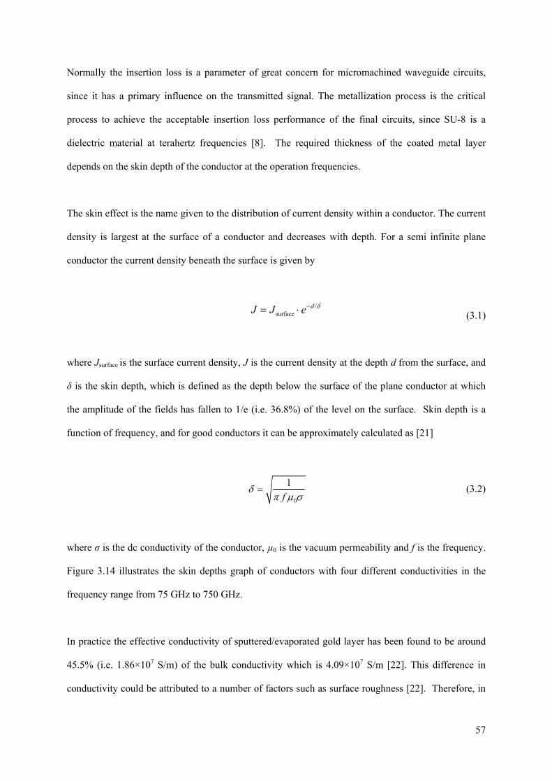
57
Normally the insertion loss is a parameter of great concern for micromachined waveguide circuits,
since it has a primary influence on the transmitted signal. The metallization process is the critical
process to achieve the acceptable insertion loss performance of the final circuits, since SU-8 is a
dielectric material at terahertz frequencies [8]. The required thickness of the coated metal layer
depends on the skin depth of the conductor at the operation frequencies.
The skin effect is the name given to the distribution of current density within a conductor. The current
density is largest at the surface of a conductor and decreases with depth. For a semi infinite plane
conductor the current density beneath the surface is given by
/surface
dJ J e (3.1)
where Jsurface is the surface current density, J is the current density at the depth d from the surface, and
δ is the skin depth, which is defined as the depth below the surface of the plane conductor at which
the amplitude of the fields has fallen to 1/e (i.e. 36.8%) of the level on the surface. Skin depth is a
function of frequency, and for good conductors it can be approximately calculated as [21]
0
1
f
(3.2)
where σ is the dc conductivity of the conductor, µ0 is the vacuum permeability and f is the frequency.
Figure 3.14 illustrates the skin depths graph of conductors with four different conductivities in the
frequency range from 75 GHz to 750 GHz.
In practice the effective conductivity of sputtered/evaporated gold layer has been found to be around
45.5% (i.e. 1.86×10⁷ S/m) of the bulk conductivity which is 4.09×10⁷ S/m [22]. This difference in
conductivity could be attributed to a number of factors such as surface roughness [22]. Therefore, in

58
Figure 3.14, two conductivities which are 45.5% of the bulk conductivities of bulk gold and bulk
silver have been considered and calculated.
From equation (3.1) it can be found that the current density at a depth which is five times the skin
depth (i.e. d=5δ ), is 0.67% of the current density at the surface. In this work, the thickness of the
coated gold or silver is 2 µm. This is greater than 5δ at frequencies from 75 GHz to 750 GHz for all
reasonable values of conductivity (as shown in Figure 3.14). Therefore, for the ideal case where 2 µm
thick metal is uniformly coated on the SU-8 layers, the thickness of the coated metal during the
metallization process will not contribute any noticeable insertion loss of the final circuits.
Figure 3.14 Skin depths of conductors with four conductivities as a function of frequency from 75
GHz to 750 GHz. These four conductivities (from highest to lowest) correspond to the conductivity of
bulk silver, bulk gold, and thin films of silver and gold, respectively.
Surface roughness is another important factor related to the insertion loss of the SU-8 micromachined
circuits, because it will increase the conductor loss due to additional scattering of electrons. As
pointed out in [32], the curves of loss as a function of surface roughness do not depend critically on
100 200 300 400 500 600 700
0.1
0.15
0.2
0.25
0.3
0.35
0.4
Ski
n D
epth
, m
Frequency, GHz
= 6.17e7 S/m = 4.09e7 S/m = 2.81e7 S/m = 1.86e7 S/m

59
the exact shape (e.g. square, rectangular or triangular) of the surface. For the sake of simplicity, the
surface roughness of the SU-8 resist has been modelled using square and equilateral triangular
grooves here, as shown in Figure 3.15 (a).
The additional loss due to surface roughness can be calculated by [8, 28]
1 2
0
21 tan (1.4( ) )c
c
(3.3)
where αc is the loss (in dB) of a conductor with a rms surface roughness of ∆, αc0 is the loss (in dB)
of a conductor with a smooth surface (i.e. ∆=0) and δ is the skin depth of the conductor computed
from equation (3.2). ∆/δ is also known as normalised rms surface roughness. Figure 3.15 (b)
illustrates the change of attenuation constant versus normalized rms surface roughness. A general
observation is that the attenuation will be nearly doubled when the surface roughness is more than two
times the skin depths. Figure 3.15 (c) shows the change of attenuation of four assumed rms surface
roughness values (i.e. 0.1, 0.2, 0.3 and 0.4 µm) at the frequencies between 75 GHz and 750 GHz.
Given the same rms roughness value, the higher the frequency, the bigger the conductor attenuation
will be. It should be pointed out that apart from equation (3.3), the change of attenuation due to
surface roughness can also be computed using other two equations, as reported in [28]. A comparison
between these three different models/equations is included in [28].
It is worth mentioning that the ratio αc/αc0 approaches an asymptotic value 2 as the normalised surface
roughness ∆/δ increases, as shown in Figure 3.15 (b). When the skin depth is small compared with the
dimensions of the grooves, the currents are forced to follow the path of the roughness profile. As
revealed in Figure 3.16 (a), the total path length on the rough surface is two times that of the smooth
surface. That is the reason why the ratio αc/αc0 asymptote is 2. Further discussion of this can be found
in [28] and [32].
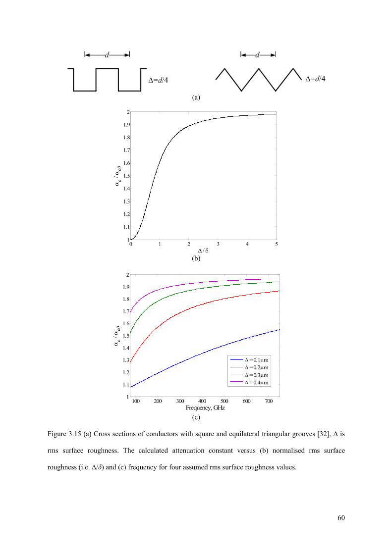
60
(a)
(b)
(c)
Figure 3.15 (a) Cross sections of conductors with square and equilateral triangular grooves [32], ∆ is
rms surface roughness. The calculated attenuation constant versus (b) normalised rms surface
roughness (i.e. ∆/δ) and (c) frequency for four assumed rms surface roughness values.
0 1 2 3 4 51
1.1
1.2
1.3
1.4
1.5
1.6
1.7
1.8
1.9
2
c /
c0
/
100 200 300 400 500 600 7001
1.1
1.2
1.3
1.4
1.5
1.6
1.7
1.8
1.9
2
c /
c0
Frequency, GHz
= 0.1 m = 0.2 m = 0.3 m = 0.4 m

61
The third important factor of the micromachined circuit performance is the thickness of each layer. As
can be seen from Figure 3.13 (c), the layer thickness is directly related to the waveguide dimension a,
which determines the cut-off frequency of the fundamental mode (i.e. TE10 mode). Therefore, the
thickness control during the fabrication should be as precise as possible. In this work, the SU-8 layer
thickness is controlled through the weight of resist, which could, in theory, offer an accuracy within ±
9 µm of the designed value because the weight is accurate up to 0.1 grams which equals to about 8.2
µm for the said resist. Unfortunately, in practice it is found that ± 20 µm is more realistic mainly due
to variation of the thickness across the wafer. This thickness variation is believed to be largely a result
of levelling inaccuracy of the hotplate. The layer thickness tolerance on the performance of the
circuits will be discussed in Chapters 4 and 5.
The alignment between two layers during the bonding process is one more essential factor for the
successful realization of layered micromachined circuits. Two types of pins have been employed to
achieve alignment between two layers during the bonding process. The first type is utilized by
micromachined circuits with bends (described in Chapter 4). Figure 3.16 (a) exhibits a SU-8 layer of a
WR-3 band waveguide with bends. The holes around the waveguide correspond to the screws and
pins of standard UG-387 flanges. During the bonding process, four precision alignment pins with a
diameter of 1.6 mm, have been fitted into the four pinholes with a diameter of 1.62 mm (as
highlighted with blue in Figure 3.16 (a)). This could result in a maximum misalignment of 20 µm
between two bonded layers.
The other type of pins is for micromachined WR-3 band circuits mounted on a metal block (presented
in detail in Chapter 5). Figure 3.16 (b) shows a SU-8 layer of a WR-3 band straight through
waveguide, in which four alignment pins with a diameter of 2 mm are inserted into the four pinholes
of the SU-8 layers during the bonding. Here again the diameter of the pinholes is 20 µm larger than
the pins.

62
Briefly, during the bonding process the alignment accuracy is in the order of 20 µm. The effect of this
possible misalignment on the circuits’ performance will be discussed in the following chapters.
Figure 3.16 Configurations of two types of SU-8 photoresist circuits in this work. The alignment
pinholes are denoted as blue in the figures.
Lastly, the air gap between bonded layers is a parameter of great interest for the micromachined
multi-layer circuits presented in this thesis. For separate SU-8 layer fabrication process, as described
in Section 3.3.1, all layers of each device are included in one mask and processed in a standard
photolithographic procedure. These separate layers are then released from silicon substrate,
gold/silver coated and finally bonded together by applying adhesive through device edges. The
disadvantage of such a method is that localized air gaps can exist after bonding because in practice the
surfaces of the SU-8 layers are not perfectly flat. These air gaps are likely to lead to increased
insertion losses due to the energy leakage. The effect of the air gap on the final device’s performance
can be relieved to certain extent by means of a second evaporation process.

63
3.4 Fully Joined SU-8 Two-Layer Fabrication Process
To eliminate the air gaps introduced during the bonding of two separate SU-8 layers, a fully joined
two-layer SU-8 processing technique has been developed in this group. The details of this two-layer
fabrication technique are presented in this section. For this fabrication technique, two SU-8 layers are
deposited successively to construct a fully joined half of the circuits, rather than making two separate
SU-8 layers and then bonding them together. Some key steps of this SU-8 two-layer processing
procedure are illustrated in Figure 3.17.
64
Figure 3.17 Some important process steps of the fully joined SU-8 two-layer fabrication technique.

65
The detailed fabrication process is described briefly in the following [23].
1. Spin Coat: A 4-inch, clean and dry silicon wafer with a thickness of 1 mm is employed as a
substrate, and a measured amount of SU-8 50 photoresist is dispensed onto the substrate
wafer followed by a spinning process.
2. Soft bake: Soft bake is performed on top of a precisely levelled hotplate and temperature is
stepped from 65°C for about 20 minutes to assist self-planarization of the SU-8 photoresist
and develop final processed layers with good thickness uniformity. Then a second baking step
at 95°C for a few hours (i.e. 4.5 hours for 432 µm thick layers, 6.5 hours for 635 µm thick
layers) is performed to drive out the inherent solvent.
3. UV Exposure: Exposure of the photoresist is performed by placing the wafer with the resist
under a mercury lamp UV sources from a Canon PLA-510 mask aligner. Mask 1 with
patterns for layer 1 together with some alignment marks is used in this step and the alignment
marks are transferred from the mask to the SU-8 resist. As mentioned before, initially signals
with wavelength less than 400 nm is filtered out by a L39 optical filter. In order to expose
through the thick SU-8 layer, the wafer with resist is subject to a multiple exposure (i.e.
expose 40 seconds and repeat for five times). The main i line (365 nm) signal is then utilised
to expose the SU-8 photoresist for 3 times 40 seconds. This is accompanied by filtering out
signals with wavelength under 360 nm through an optical PL360 filter.
4. Post Exposure Bake: The wafer with resist is then softly baked at 70°C for 15 minutes, the
main purpose of which is to allow weak cross-linking in SU-8 resist and at the same time
avoid too much stress between the cross-linked SU-8 resist and the silicon substrate.
5. 2nd Spin Coating and Soft Bake: The same amount of fresh SU-8 as the one used in Step 1 is
then added on top of the resist and wafer. Then the fresh solvent is softly baked at 70°C for

66
about 9 hours. Again, this lower temperature baking step is introduced to relieve the stress
between the SU-8 resist and the silicon substrate. The second resist layer is then aligned
precisely and placed on top of the first resist layer under the mask aligner.
6. 2nd UV Exposure: The second exposure process is basically the same as the one performed for
the first layer, apart from alignment. The alignment is achieved by aligning the marks on the
mask 2 to the marks on the first exposed SU-8 resist layer as explained early. At the second
exposure stage, the long wavelength signal lines from the mercury lamp are able to penetrate
through both SU-8 layers to reach silicon substrate, therefore both layers are cross-linked and
joined together during the second post exposure baking stage.
7. 2nd Post Exposure Bake: After the second exposure, the wafer with the resists is post exposure
baked at 65°C for 5 minutes followed by 95°C for 30 minutes to ensure strong cross-linking
across all the exposed areas of both SU-8 photoresists.
8. Development and Silicon Substrate Removal: The wafer with resists is then developed in EC
solvent for 45 minutes to etch away the non-crosslinked SU-8. After the development the SU-
8 resists are released from silicon substrate in sodium hydroxide (i.e. NaOH) solution. Then
running de-ionized water is applied to clean the SU-8 resists for 2 minutes, which is followed
by ultrasonic bath for 15 minutes. These pieces are then blown dry.
9. Metallization: These SU-8 pieces are then loaded into a vacuum chamber for metallization.
The metallization process is the same as the one for single SU-8 layer fabrication process
described in Section 3.3.1. Cressington 308 metal coater is employed for metallization, which
begins with oxygen plasma cleaning for 45 seconds, followed by a thin Cr sputtering layer of
around 5 nm for much improved adhesion. Eventually a 2 µm thick silver layer is thermally
evaporated onto the surface of the device to form the coated conducting layer. In order to

67
achieve good sidewall metal coating, the sample holder rotates continuously at a tilted angle
during the metallization process.
This fully joined two-layer SU-8 fabrication process addresses the air gap problem of separate SU-8
fabrication process perfectly. However, the final assembled circuit’s performance still depends on
many factors during the fabrication such as sidewall surface roughness, dimensional accuracy, layer
thickness control and alignment between two halves of the circuits, etc. Detailed discussions of the
influences of some of these factors will be presented in Chapters 4 and 5 for each micromachined
circuits.
3.5 Conclusions
This chapter has provided a general introduction to terahertz wave applications, and an introduction to
some recently developed micromachining techniques. A separate SU-8 single-layer fabrication
process was employed to fabricate some of the micromachined waveguide circuits presented in this
thesis. Details of the fabrication process, as well as a discussion of some important factors during the
fabrication, were presented in this chapter. This chapter also described a fully joined two-layer SU-8
fabrication process. This was developed in the EDT group to address the problem of localized air gaps
between two bonded layers, associated with the separate single-layer fabrication process.
The two-layer SU-8 fabrication process described in Section 3.4, is included in our paper [23]
submitted to IEEE Transactions on Microwave Theory and Techniques. All the fabrication work in
this thesis was performed by Dr. Maolong Ke in the Emerging Device Technology (EDT) research
group, the University of Birmingham.

68
References
[1] Lee Yun-Shik: Principles of Terahertz Science and Technology (2009 Springer Science and
Business Midia, LLC)
[2] Dobroiu A., Otani C., Kawase K.: ‘Terahertz-Wave Sources and Imaging Applications,’
Measurement-Science and Technology, 2006, 17, pp. 161-174
[3] Zhang X.C.: ‘Terahertz Wave Imaging: Horizons and Hurdles,’ Physics in Medicine and Biology,
2002, 47, pp. 3667-3677.
[4] Liu D., Gaucher B., Pfeiffer U., Grzyb J.: Advanced Millimeter-Wave Technologies: Antenna,
Packing and Circuits (2009 John Wiley & Sons Ltd.)
[5] Appleby R., Wallace H.: ‘Standoff Detection of Weapons and Contraband in the 100 GHz to 1
Terahertz Region,’ IEEE Trans. Antennas and Propagation, 2007, 55, 11, pp.2944-2956.
[6] Fitzgerald A., Pickwell E., Wallace V.: ‘Medical Applications of Broadband Terahertz Pulsed
Radiation,’ Lasers and Electro Optics Society annual meeting, 2005, pp. 120-121
[7] Bruneau P. J., Janzen H. D., Ward J. S.: ‘Machining of Terahertz Split-Block Waveguides with
Micrometer Precision,’ 33rd International conference on IRMMW-Terahertz , 2008.
[8] Li Y., Mehdi I., Maestrini A., Lin R. H., Papapolymerou J.: ‘ A Broadband 900 GHz Silicon
Micromachined Two-Anode Frequency Tripler,’ IEEE Trans. Microw. Theory Tech., 2011, 59, (6),
pp.1673-1681.
[9] Biber S., Schur J., Hofmann A., Schmidt L. P.: ‘Design of New Passive THz Devices Based on
Micromachining Techniques.’ MSMW Symposium Proceeding, June 2004, pp. 26-31.
[10] Hsu Tai-Ran, MEMS and Microsystems: Design, Manufacture, and Nanoscale Engineering (2nd
edition, Wiley)
[11] Gentili E., Tabaglio L., Aggogeri F.: ‘Review of Micromachining Techniques,’ Proceedings of
the 7th International Conference on Advanced Manufacturing Systems and Technologies, 2005
[12] Mcgrath W.R., Walker C., Yap M., Tai Y.C.: ‘Silicon Micromachined Waveguides for
Millimeter Wave and Submillimter-Wave Frequencies,’ IEEE Microw. Guided Wave Letters. 1993,
3, (3), pp.61-63.
[13] Roberstson S., Katehi L. and Rebeiz G.: ‘Micromachined W-band Filters,’ IEEE Trans. Microw.
Theory Tech., 1996, 44, (4), pp. 598-606.
[14] Biber S., Schur J., Schmidt L.P.: ‘Technological Issues for Micromachining of New Passive THz
Components Based on Deep Trench Silicon Etching,’ Infrared and Millimeter Waves, 12th
International Conference on Terahertz Electronics, 2004, pp. 145 – 146.
[15] Li Y., Kirby P.L., Offranc O., Papapolymerou J.: ‘Silicon Micromachined W-band Hybrid
Coupler and Power Divider using DRIE Technique,’ IEEE Microw. Wireless Compon. Lett. 2008, 18,
(1), pp. 22-24.

69
[16] Conradie E. H., Moore D. F.: ‘SU-8 Thick Photoresist Processing as A Functional Material for
MEMS Applications,’ Journal of Microw. and Microenginnering, 2002, 12, pp. 368-374
[17] Seidemann V., Butefisch S., Buttgenbach S. : ‘Fabrication and Investigation of in-line Compliant
SU8 Structures for MEMS and Their Application to Micro Valves and Micro Grippers,’ Sensors and
Actuators, 2002, A 97-98, pp. 457-461.
[18] Levinson H. J., Principles of Lithography (second edition, 2005, SPIE the International Society
for Optical Engineering)
[19] Suzuki K., Smith B. W.: ‘Microliehography Science and Technology,’ (second edition, 2007,
CRC Press, Talyor & Francis Group)
[20] Banks D., Microengineering, MEMS, and Interfacing, a practical guide (2006, CRC Press)
[21] Pozar D., Microwave Engineering (third edition, 2005 John Wiley & Sons)
[22] Batt R.J., Jones G.D., Harris D.J.: ‘The Measurement of the Surface Resistivity of Evaporated
Gold at 890 GHz’, IEEE Trans. Microw. Theory Tech., 1977, 25, (6), pp. 488-491
[23] Ke M.L., Shang X.B., Wang Y., Lancaster M.J.: ‘High Performance WR-3 Band Waveguide
Devices using SU-8 Photoresist Micromachining Technology,’ Submitted to IEEE Transaction on
Microwave Theory and Techniques.
[24] http://exitech.org/pdfFiles/Excimer%20Laser%20Microfabrication%20and%20Micromachining.pdf
[25] Malek C.K., Saile V.: ‘Applications of LIGA technology to precision manufacturing of high-
aspect-ratio micro-components and systems: a review,’ Microelectronics Journal, 2004, 35, pp. 131-
143.
[26] Varadan V.K., Vinoy K.J., Jose K.A., RF MEMS and Their Applications (2003, John Wiley &
Sons Ltd)
[27] Li Y., Papapolymerou J.: ‘Silicon Micromachined W-Band Folded and Straight Waveguides
Using DRIE Technique,’ in Microwave Symposium Digest, 2006, IEEE MTT-S International, pp.
1915-1918.
[28] Lukic M.V., Filipovic D.S.: ‘Modelling of 3-D Surface Roughness Effects with Application to
Coaxial Line,’ IEEE Trans. Microw. Theory Tech., 2007, 55, (3), pp.518-525.
[29] Collins C.E., Miles R.E., Digby J.W. etc,: ‘ A New Micro-Machined Millimeter-Wave Terahertz
Snap-Together Rectangular Waveguide Technology,’ IEEE Microw. Guided Wave Lett., 1999, 9, (2),
pp. 63-65.
[30] Pan B., Li Y., Tenezeris M. M., Papapolymerou J.: ‘Surface Micromachining Polymer-Core-
Conductor Approach for High-Performance Millimeter-Wave Air-Cavity Filters Integration,’ IEEE
Trans. Microw. Theory and Tech., 2008, 56, (4), pp.959-970.
[31] http://www.microchem.com/pdf/SU-82000DataSheet2000_5thru2015Ver4.pdf
[32] Morgan S. P.: ‘Effect of Surface Roughness on Eddy Current Losses at Microwave Frequencies,’
Journal of Applied Physis, 1949, 20, pp. 352-362

70
Chapter 4
Micromachined Waveguide Circuits Measured with Bends
This chapter describes the SU-8 micromachined waveguide circuits measured with two H-plane back-
to-back bends. These bends are introduced to help the connections between the micromachined
waveguide circuits and the external flanges of the network analyzer. Section 4.1 provides a review of
some recent terahertz micromachined waveguide devices with operating frequencies from WR-10
band (i.e. W-band) to WR-3 band. Section 4.2 explains the principles of the bend measurement
methods employed by the micromachined circuits presented in this chapter. Section 4.3 presents the
design and measurement of a WR-10 band through waveguide and a WR-10 band fourth order
Chebyshev filter. Both of these two circuits are fabricated using the separate SU-8 single-layer
process. Section 4.4 is devoted to presenting the designs and measurements of three WR-3 band
micromachined circuits: a through waveguide, a fourth order Chebyshev bandpass filter and an eighth
order dual-band filter. The through waveguide and the Chebyshev filter are fabricated using both the
separate SU-8 single-layer technique and the joint two-layer process. The measurement results are
presented, and a comparison between the results from different fabrication processes is given. Section
4.5 describes the design of a WR-1.5 band (500-750 GHz) third order Chebyshev bandpass filter. This
is followed by a conclusion given in Section 4.6.
4.1 Literature Review
As mentioned in Chapter 3, in recent years several different micromachining techniques, such as
DRIE, LIGA and thick SU-8 photoresists technology, have been developed to replace the traditional
CNC metal milling for the fabrication of terahertz waveguide circuits. Additionally, the measurement
of micromachined waveguide devices operating at terahertz frequencies is challenging due to the
difficulties in the interconnection with standard waveguide flanges. A wide range of micromachined
terahertz waveguide circuits and measurement methods have been reported in literature. This section
71
presents a general review of the published work with regard to waveguides and cavity filters operating
at WR-10 band and WR-3 band.
In [1], a silicon WR-10 band 3rd order bandpass filter, fabricated using the DRIE technology, with a
measured centre frequency of 92.45 GHz and a measured fractional bandwidth of 4.83%, is presented
by the Georgia Institute of Technology. This filter has a length of 25.4 mm and it is designed to have
a centre frequency of 94.2 GHz and a fractional bandwidth of 3.5%. The measured passband insertion
loss of this filter is between 1.1 dB and 1.3 dB. The measured return loss is better than 10 dB across
the whole passband. A special fixture, which consists of two separate metal blocks, has been
employed for the measurement of the micromachined filter. During the measurement, the
micromachined filter is sandwiched between these two blocks, as shown in Figure 4.1 (a). To achieve
the connection with the network analyzer, two standard WR-10 band waveguide flanges are patterned
on the front and back face of the assembled fixture [1].
In [2], the University of California at Berkeley presents a 25.4 mm long WR-10 band plastic
waveguide fabricated using a micro hot embossing process in conjunction with a metallic
electroplating technique. This waveguide is measured to have an insertion loss of 1.35 dB or 0.053
dB/mm and a return loss of better than 20 dB in the majority of WR-10 band. A plastic flange,
fabricated using the same hot embossing process, is integrated with the waveguide to facilitate the
connection from the waveguide to the network analyzer, as shown in Figure 4.1 (b).
Later, the same group presents a WR-10 band 5th order Chebyshev filter with a measured passband
insertion loss of 1.22 dB and a measured passband return loss of 9.3 dB [3]. This filter shows a
measured bandwidth of 3.15% centred at 96.77 GHz, against the simulated bandwidth of 3.62%
centred at 96.63 GHz. The same polymer micro hot embossing process together with the metallic
electroplating technique is employed to fabricate this filter [3].

72
Figure 4.1 Configurations of the reviewed micromachined circuits. (a) Photograph of the silicon filter
mounted in a brass fixture [1]. (b) Photograph of the assembled W-band circuits [2-3]. (c) Schematic
view of the filter with current probe [4]. (d) Half of the assembled SU-8 waveguide [5]. (e) Illustration
of the flanges patterned with photonic bandgap structures and the SU-8 waveguide [7]. (f) Photograph
of the measurement setup for the WR-3 band SU-8 waveguide [8]. (g) (left) Illustration of the
micromachined circuits with KMPR resist flanges; (right) Photograph of the assembled circuits [9].
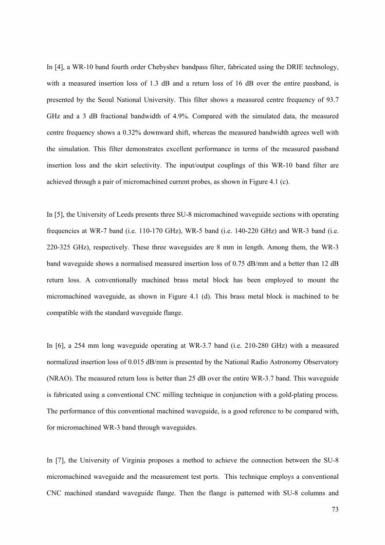
73
In [4], a WR-10 band fourth order Chebyshev bandpass filter, fabricated using the DRIE technology,
with a measured insertion loss of 1.3 dB and a return loss of 16 dB over the entire passband, is
presented by the Seoul National University. This filter shows a measured centre frequency of 93.7
GHz and a 3 dB fractional bandwidth of 4.9%. Compared with the simulated data, the measured
centre frequency shows a 0.32% downward shift, whereas the measured bandwidth agrees well with
the simulation. This filter demonstrates excellent performance in terms of the measured passband
insertion loss and the skirt selectivity. The input/output couplings of this WR-10 band filter are
achieved through a pair of micromachined current probes, as shown in Figure 4.1 (c).
In [5], the University of Leeds presents three SU-8 micromachined waveguide sections with operating
frequencies at WR-7 band (i.e. 110-170 GHz), WR-5 band (i.e. 140-220 GHz) and WR-3 band (i.e.
220-325 GHz), respectively. These three waveguides are 8 mm in length. Among them, the WR-3
band waveguide shows a normalised measured insertion loss of 0.75 dB/mm and a better than 12 dB
return loss. A conventionally machined brass metal block has been employed to mount the
micromachined waveguide, as shown in Figure 4.1 (d). This brass metal block is machined to be
compatible with the standard waveguide flange.
In [6], a 254 mm long waveguide operating at WR-3.7 band (i.e. 210-280 GHz) with a measured
normalized insertion loss of 0.015 dB/mm is presented by the National Radio Astronomy Observatory
(NRAO). The measured return loss is better than 25 dB over the entire WR-3.7 band. This waveguide
is fabricated using a conventional CNC milling technique in conjunction with a gold-plating process.
The performance of this conventional machined waveguide, is a good reference to be compared with,
for micromachined WR-3 band through waveguides.
In [7], the University of Virginia proposes a method to achieve the connection between the SU-8
micromachined waveguide and the measurement test ports. This technique employs a conventional
CNC machined standard waveguide flange. Then the flange is patterned with SU-8 columns and

74
photonic bandgap structures, as shown in Figure 4.1 (e). The SU-8 columns are for alignment between
the micromachined circuits and flanges, whereas the photonic bandgap structures are introduced to
reduce the effect of the possible air gap between them. HFSS simulation results demonstrate that, by
employing these photonic bandgap structures, a gap of 20 µm can be tolerated and still have a return
loss better than 15 dB [7]. No measurement results are reported in [7].
In [8], a SU-8 micromachined WR-3 band straight waveguide with a length of 11.4 mm is reported by
the University of Virginia. This waveguide is measured to have a normalised insertion loss of 0.263
dB/mm and a better than 15 dB return loss. The measurement setup is shown in Figure 4.1 (f). As
stated in [8], a loose connection between the flange and the face of the SU-8 miromachined
waveguide, may contribute extra measured insertion loss of the waveguide section.
Later, the same research group demonstrates a 23.8 mm long WR-3 band waveguide and an 18.75 mm
long WR-3 band low-pass waveguide filter in [9]. Both circuits are fabricated using KMPR UV LIGA
process. KMPR is another kind of photoresist that is similar to SU-8. Compared with SU-8, it is less
susceptible to delamination, adheres better to metal, and is easier to remove from a silicon substrate
[10]. The KMPR WR-3 band waveguide shows a measured normalised insertion loss of 0.096 dB/mm
and a better than 13.5 dB return loss. The KMPR WR-3 band low-pass filter is measured to have a
1.82 dB insertion loss and a better than 10 dB return loss over the entire passband. During the
measurement, the two halves of the KMPR resists are aligned and mounted together with aluminium
blocks, as shown in Figure 4.1 (g). Then the waveguide faces are polished, prior to patterning a
KMPR ring on top of them. Dowel pin holes and screw holes are then machined to fit the standard
waveguide flanges from the network analyzer.
A table, which shows the performance comparison of the above reviewed published work and the
work presented in this thesis, is given in Chapter 7.

75
4.2 Principles of Bend Measurement Method
In this work, in order to achieve reliable and accurate interconnection with standard waveguide
flanges, two H-plane back-to-back bends are embedded in the designs of the SU-8 waveguide or filter.
Figure 4.2 shows an illustration of the bend measurement method.
Figure 4.2 Illustration of the bends measurement method. The pinholes inside the SU-8 circuits and
brass plates are omitted to provide a clear view. a is the waveguide broadside wall dimension.
During the measurement, the micromachined circuits are sandwiched between two brass plates, as
shown in Figure 4.2. Standard waveguide flanges (i.e. UG-387) are inserted into the opening on the
brass clamping structure to connect directly with the micromachined waveguide circuits. Screws on
the flanges go straight through the micromachining circuits and into nuts at the opposite plate. The
alignment pins address the accuracy to which the layers are aligned as well as the accuracy to which
the circuit is aligned to the external flange. The screws are used to clamp the layers together as well
as fixing the external flange to the micromachined waveguide. The length of the micromachined SU-8
waveguide circuit is sufficiently long to allow fair separation between the flanges of the measurement
equipment to avoid blocking of pins and screws from the other side.

76
The brass plates are fabricated using the conventional CNC machining. They are the mechanical
supporting and clamping fixture and bear no alignment function here, and therefore the alignment
accuracy of the micromachined devices is not affected by the machining tolerance of the brass plates.
This bend measurement method has three principal advantages: (i) the flanges of the SU-8 circuits are
fabricated using the SU-8 micromachining process, therefore they have high dimensional accuracy; (ii)
the SU-8 circuits can be screwed to the flanges of the network analyser to ensure an intimate contact
(i.e. without air gap); (iii) accurate alignments between the external flanges and the SU-8 circuits can
be achieved through the alignment pins of the flanges. However, there are also some drawbacks
associated with this bend measurement method. They are (i) extra insertion loss brought by these two
bends; (ii) non-perfect matches (i.e. increased reflection coefficient) caused by the bend structures.
The second drawback can be overcome by developing a bend structure with a good wide band match.
This bend measurement method can be employed by micromachined waveguide circuits with
operating frequencies from 100 GHz up to 300 GHz and beyond.
4.3 Micromachined WR-10 Band Components With Bends
In this section, two WR-10 band waveguide circuits (i.e. a straight through waveguide and a bandpass
filter), fabricated using the separate SU-8 single-layer process, are presented. Both circuits are
formed with six gold-coated SU-8 layers with the same thickness of 0.635 mm. Two specially
designed H-plane bends, which are compatible with the layered structures, have been integrated into
the design of the waveguide and filter to achieve a tight and accurate connection with external
standard flanges.
Subsection 4.3.1 presents the design of the bend structures and the performance of the SU-8
waveguide with bends. The details of the SU-8 bandpass filter with bends are described in Section

77
4.3.2. The last subsection 4.3.3 provides a discussion of the asymmetrical rejection responses of the
waveguide filters coupled by all-capacitive irises.
4.3.1 WR-10 band waveguide
Figure 4.3 (a) A schematic of the WR-10 band through waveguide with two back-to-back H-plane
bends as modelled in CST, the blue part is vacuum which is surrounded by perfect electric conductor
(PEC) in the simulation. The thickness of each of the six layers is 0.635 mm. a = 2.54 mm, b = 1.27
mm. (b) Cross section veiw of the micromachined waveguide which consists of six gold-coated SU-8
layers. (c) Top view of the first layer. (d) Top view of the second layer.
Two specially designed H-plane back-to-back bends are adopted by both of the waveguide and filter
for easily connection with the network analyser, as shown in Figure 4.3 (a). The waveguide with the
bends has been made of six layers with the same layer thickness of 0.635 mm, as shown in Figure 4.3

78
(b). Figure 4.3 (c, d) illustrate the top view of the first and second layer, in which the holes around the
waveguide are fitting to screws and the alignment pins of standard UG-387 waveguide flanges.
Multi-stepped and multi-mitred corners are conventional approachs to design a 90º bend with
broadband matching in waveguides. However, neither of these structures are compatible with the
multi-layered SU-8 micromachining technology used here. As shown in Figure 4.3 (a), a novel bend
is developed to meet this specical requirement. The strutures around the bend have been designed to
achieve a good match across the whole WR-10 band. The dimensions and the characteristics of one
bend simulated by CST [11] can be found in Figure 4.4 and Figure 4.5 respectively. A similar bend
strucure has been reported in [12]. The differences are that in [12] the bend is split into two pieces
and machined by CNC metal milling.
Figure 4.4 Dimensions of the H-plane bend: (a) bottom view of bend (b) front view of bend. d1=0.199,
d2=1.033, d3=1.793. Unit: mm

79
Figure 4.5 Simualtion results of one H-plane bend
The simulation result of the bend shows a return loss better than 22.5 dB across the whole WR-10
band. The resonant frequency and bandwidth of this bend depend on the dimensions of d1,d2 and d3.
The total length of the WR-10 band waveguide including a pair of back-to-back H-plane bends is 18
mm and the simualted performance can be found in Figure 4.7.
Figure 4.6 (a) final assembled WR-10 band SU-8 wavguide with bends; (b) the measurement setup .
75 80 85 90 95 100 105 110
-35
-30
-25
-20
-15
-10
-5
0
S P
aram
eter
s, d
B
Frequency, GHz
Simulated S
11
S21

80
The WR-10 band waveguide with bends is fabricated using the separate SU-8 single-layer
micromachinig technique described in Section 3.3. After metal coating, the top three pieces are
aligned using alignment pins before being bonded together with silver loaded epoxy around the edges.
A second metal evaporation is performed to mitigate the effect of the possible air gaps and minimize
the resistive losses on the joined surfaces. The same procedure is repeated for the bottom three layers.
A photograph of the assembled device is shown in Figure 4.6 (a). The two halves of SU-8 pieces are
assembled by clamping together two brass plates, during which pins are employed to align these two
SU-8 pieces and screws on the brass plates are tightened to ensure a good contact between them.
The S parameter measurements of the WR-10 band waveguide and the filter (discussed in the next
section) are carried out on an Agilent N5250A Network Analyzer subject to a Through-Reflect-Line
(TRL) calibration. During the measurement, the micromachined circuits are sandwiched between the
two brass plates, as shown in Figure 4.6 (b). Standard UG-387 waveguide flanges of the network
analyzer are inserted into the opening on the brass clamping structure to connect directly with the
micromachined waveguide. As can be seen in Figure 4.6 (b), screws on the flanges go through the
micromachined waveguide and into nuts at the opposite plate. Screws and alignment pins are
employed to provide an accurate and secure connection between the SU-8 micromachined waveguide
and the standard waveguide flanges of the network analyser.

81
Figure 4.7 The measured and simulated results of the WR-10 band through waveguide with two H-
plane back-to-back bends. A conductivity of 1.86×10⁷ S/m is employed in this simulation. This
through waveguide is fabricated using the separate SU-8 single layer process.
The S parameter measurement results of the through waveguide with bends are shown in Figure 4.7,
which shows that the measured return loss is better than 20 dB in the majority of the WR-10 band.
The measured insertion loss is between 0.38 dB and 0.6 dB across the whole WR-10 band. The
averaged insertion loss of 0.5 dB corresponds to an antenuation of 0.0278 dB/mm. The insertion loss
of a commercial standard machined WR-10 band metal waveguide is around 0.0024 to 0.0035 dB/mm
[13]. As mentionied in Chapter 3, the conductivity of the thin-film-gold is 45.5% of the conductivity
of the block gold (i.e. 4.09×10⁷ S/m). Therefore, a conductivity of 1.86×10⁷ S/m has been employed
in the simulations carried out in this work. According to the CST simulation results, this conductivity
gives 0.09 dB insertion loss for the through waveguide with bends. The rest of the loss (around 0.4 dB)
is believed to attribute to the energy leakage at the interfaces of bonded layers. Since localized air gap
may be introduced during the bonding process, as discussed in Chapter 3.
75 80 85 90 95 100 105 110-3.5
-3.0
-2.5
-2.0
-1.5
-1.0
-0.5
0.0
-70
-60
-50
-40
-30
-20
-10
0
S21
Simulated
S21
Measured
|S21
| , d
B
Frequency , GHz
S11
Simulated
S11
Measured
|S11 | , dB

82
4.3.2 WR-10 band filter
An all capacitive-iris coupled WR-10 band filter with a Chebyshev response is presented. This filter
consists of four resonators operating in the TE101 mode separated by asymmetrically placed capacitive
irises. This waveguide filter is designed to have a central frequency of 90 GHz and a 3 dB bandwidth
of 10.2 GHz (a fractional bandwidth of 11.3%). A filter synthesis technique, as described in Chapter 2
and [14], has been followed to design this filter. In this method the external Q and the coupling
coefficients between the resonators are calculated from the specification of the filter. They are found
to be Qext=9.1659, k12=0.0841, k23=0.0618, k34=0.0841. In the actual physical waveguide filter, the
external Q is dependent upon the width of the gap in the capacitive iris of the resonators coupled to
the feed waveguide. The required gap size to get an external Q of 9.1659 is found from simulation in
CST microwave studio, using simulations on one resonator. Similarly, the coupling coefficients are
dependent upon the physical size of the capacitive iris between the resonators, so this is adjusted in
CST (using two resonators) to achieve the required coupling coefficients. Details of the iris-coupled
waveguide filter design procedure are provided in Chapter 2.
The full-wave modelling is carried out in CST and Figure 4.8 gives the dimensions of this filter after
CST optimisation.
Figure 4.8 A schematic side-view diagram of the 4th order iris filter (drawing is not to scale). Some
critical dimensions of the fourth order capacitive iris coupled filter. h1= 0.47 mm, h2=0.84 mm, h3=
0.95 mm, L1=2.517 mm, L2=2.382 mm, b=1.27 mm, a=2.54 mm. All irises have the same thickness t
of 0.5 mm.

83
It should be noted that the coupling iris employed in this filter is asymmetrical, which is different
from the conventional choice for waveguide filters at lower frequencies. The benefit of using
asymmetrical irises compared with symmetrical ones is an increase in the gaps (i.e. g1, g2, g3) of the
coupling irises. For simplicity, these two kinds of capacitive coupling irises can be represented here
by a single shunt capacitor as shown in Figure 4.9 [15].
Figure 4.9 Diagram of (a) a symmetrical iris, (b) an asymmetrical iris and (c) their equivalent circuit,
bc is the capacitive susceptance.
For symmetrical capacitive iris the capacitive susceptance is [15]:
2
2 2
2 (1.1 ' 0.57 ) ( ')
4 ( ')gc
b d t b d t tb
b b b d
(4.1)
and for asymmetrical capacitive iris this is [15]:
2
2 2
2 (1.1 ' 0.57 ) ( ')
2 ( ')gc
b d t b d t tb
b b b d
(4.2)
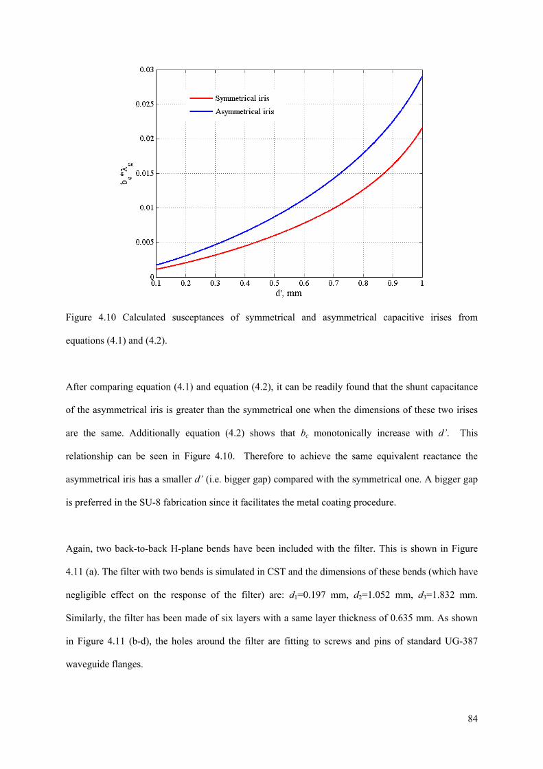
84
Figure 4.10 Calculated susceptances of symmetrical and asymmetrical capacitive irises from
equations (4.1) and (4.2).
After comparing equation (4.1) and equation (4.2), it can be readily found that the shunt capacitance
of the asymmetrical iris is greater than the symmetrical one when the dimensions of these two irises
are the same. Additionally equation (4.2) shows that bc monotonically increase with d’. This
relationship can be seen in Figure 4.10. Therefore to achieve the same equivalent reactance the
asymmetrical iris has a smaller d’ (i.e. bigger gap) compared with the symmetrical one. A bigger gap
is preferred in the SU-8 fabrication since it facilitates the metal coating procedure.
Again, two back-to-back H-plane bends have been included with the filter. This is shown in Figure
4.11 (a). The filter with two bends is simulated in CST and the dimensions of these bends (which have
negligible effect on the response of the filter) are: d1=0.197 mm, d2=1.052 mm, d3=1.832 mm.
Similarly, the filter has been made of six layers with a same layer thickness of 0.635 mm. As shown
in Figure 4.11 (b-d), the holes around the filter are fitting to screws and pins of standard UG-387
waveguide flanges.

85
Figure 4.11 Configuration of the designed filter. (a) The simulation model in CST. The blue part is
vacuum which is surrounded by perfect electric conductor (PEC) in the simulation; (b) The first/sixth
layer; (c) The second /fifth layer; (d) The third /fourth layer.
Figure 4.12 The measured and simulated results of the WR-10 band waveguide filter with two H-
plane back-to-back bends. A conductivity of 1.86×10⁷ S/m is employed in this simulation. This
waveguide filter is fabricated using the separate SU-8 single layer process.
75 80 85 90 95 100 105 110-50
-40
-30
-20
-10
0
S P
aram
eter
s , d
B
Frequency , GHz
S11
(Simulated)
S21
(Simulated)
S11
(Measured)
S21
(Measured)

86
The CST simulation results of this waveguide filter are displayed in Figure 4.12. This all-capacitive
iris coupling structure is not suitable for filters requiring small couplings. Since the capacitive iris
itself is a section of propagating waveguide, it causes a relatively strong coupling even with small
gaps [16]. Furthermore, in contrast to an inductive-iris filter, filters with capacitive irises show a
higher rejection in the upper stop-band, but a lower rejection in the frequency range close to the cut-
off of the feeding waveguide [17], as shown in Figure 4.12. This phenomenon will be discussed in
detail in Section 4.3.3.
The measured responses of the filter with two bends are shown in Figure 4.12. The measured central
frequency of the filter is shifted downward by 1.53 GHz, from the simulated 90 GHz to the measured
88.47 GHz. The measured 3 dB bandwidth is 8.61 GHz whereas the simulated one is 10.2 GHz. The
measured passband insertion loss of this WR-10 band filter is between 0.97-1.1 dB and passband
return loss is better than 15 dB. Generally the measured performance of this filter agrees well with
simulations. CST simulation indicates that the centre frequency of the filter shifts downward with a
rate of about 0.056 GHz/µm when the thickness of each layer increases. Each of the SU-8 pieces is
found to be about 10-15 µm thicker than the designed value of 635 µm which contributes to a 0.84
GHz frequency shift. Small errors in the CST simulation and a possible air gap between each of these
layers may result in the remaining 0.69 GHz frequency shift.
4.3.3 Discussion of capacitive iris coupled waveguide filters
In this work, capacitive coupling irises have been used to provide filter external couplings as well as
internal resonator couplings. The all-capacitive-iris-coupled bandpass filter has a bad rejection at the
frequencies around the cut-off of the rectangular waveguide, as can be observed in Figure 4.12.
Figure 4.13 shows the CST simulation results of the above WR-10 band filter over a wider frequency
from 59.02 GHz to 110 GHz. The start frequency 59.02 GHz is the dominant TE10 mode cut-off
frequency of a WR-10 band rectangular waveguide. As can be seen in Figure 4.13, another passband

87
occurs in the region around the cut-off frequency. This passband at the cut-off has an impact on the
left skirt of the designed filter centred at 90 GHz. This unique response associated with the capacitive
iris coupled filter is due to the fact that capacitive irises are in fact resonating at the TE10 mode cut-off
frequency [18].
Figure 4.13 Simulation results of the WR-10 band filter without bends over a wider frequency range
from 59.02 GHz to 110 GHz.
When considered over the complete frequency range, the asymmetrical capacitive coupling iris, as
shown in Figure 4.9 (b), can be modelled as a shunt susceptance given by [18]:
24 1 ( ')( ) ln csc( )
2
b b dB
a b
(4.3)
where all the parameters have the same meanings as denoted in Figure 4.9 (b). From equation (4.3),
the frequency, at which B equals to zero, can be extracted as
60 70 80 90 100 110-60
-40
-20
0
S P
aram
eter
, dB
Frequency, GHz
S11(Simulated)
S21(Simulated)

88
0 0.5
1
( )a
(4.4)
It can be observed that ω0 is the angular TE10 mode cut-off frequency. Above ω0, B holds a positive
value. This leads to the well-known conclusion that the iris is a capacitive susceptance [18]. At the
frequency below cut-off ω0, B changes to a negative value. This corresponds to an inductive
susceptance. The equivalent susceptance of the capacitive iris, B, is zero at the cut-off frequency ω0,
in other words the capacitive iris is resonating at ω0. This is the reason why bandpass filters coupled
by all-capacitive irises show a low rejection in the frequency range close to the TE10 cut-off of the
feeding waveguide.
In contrast, the susceptance of an asymmetrical inductive coupling iris is given by [18]
2 22 ( ') ( ')cot 1 csc
2 2
a d a dB
a a a
(4.5)
Figure 4.14 Illustration of an asymmetrical inductive coupling iris.
The physical meanings of the parameters in equation (4.5) are given in Figure 4.14. A general
observation from equation (4.5) is that the susceptance of the inductive iris always holds a negative
value. This indicates that the inductive iris always corresponds to an inductive susceptance, even at
frequencies below cut-off. Therefore, for all-inductive-iris-coupled bandpass filters, the rejection in
the lower stopband monotonically increases with decreasing frequency.

89
4.4 Micromachined WR-3 Band Components With Bends
This section presents three WR-3 band SU-8 micromachined circuits: a through waveguide, a fourth
order Chebyshev filter and an eighth order dual-band filter, which are described in Sections 4.4.1,
4.4.2, 4.4.3, respectively. These three circuits employ a pair of H-plane bends to help the connection
with measurement systems, and all of them are comprised of four SU-8 layers with the same thickness
of 0.432 mm. The through waveguide and the Chebyshev filter are fabricated using both the separate
single-layer and the joint two-layer processes. Comparisons between the measurement results of the
circuits from different fabrication processes are given in Sections 4.4.1 and 4.4.2. The dual-band filter
is fabricated using the two-layer process, as it cannot be constructed with the single-layer process due
to the isolated parts/regions in the filter structure.
4.4.1 WR-3 band through waveguide
Figure 4.15 Configurations of the WR-3 waveguide with two embedded H-plane back-to-back bends.
(a) the whole structure; (b) detail view of the bend structure; (c) top view of the first/fourth gold
coated SU-8 layer; (d) top view of the second/third gold coated SU-8 layer. Unit: mm

90
A WR-3 band through waveguide is constructed with four gold or silver-coated SU-8 layers, each of a
thickness of 0.432 mm. These layers are assembled to form the waveguide. Again, two
micromachined back-to-back H-plane bends are embedded in the designs of the micromachined
waveguide to achieve reliable and accurate interconnection with standard waveguide flanges, as
shown in Figure 4.15 (a). Such a bend configuration has been implemented before in a 300 GHz
micromachined waveguide as reported by our research group in [19]. However, a different wideband
matching structure containing only curved edges, which facilitates the fabrication procedure, is
introduced here, and is shown in Figure 4.15 (b). Fig. 15 (c, d) illustrates the top view of the first and
second layer, in which the holes for the waveguide screws and alignment pins of standard UG-387
waveguide flanges are shown. The size of each SU-8 layer is 48 mm × 24 mm × 0.432 mm.
This WR-3 band SU-8 waveguide with bends is assembled using the same process as the
micromachined WR-10 waveguide described in Section 4.3.1. Figure 4.16 shows the measurement
setup of the micromachined WR-3 band waveguide circuits with bends. The measurements are carried
out on an Agilent E8361A Network Analyzer with a WR-3 extension T/R module at test port 1 and a
receive-only T module at test port 2. Enhanced response calibrations, which combine a one-port
calibration and a response calibration, are performed before measurements.
Figure 4.16 Photograph of the measurement setup for the WR-3 band waveguide circuits with bends

91
This WR-3 band through waveguide with bends has been made using both the single-layer and two-
layer SU-8 fabrication process. Their corresponding measurement results together with CST
simulation results are exhibited in Figure 4.17. The waveguide with bends, fabricated using the single-
layer process, shows a measured insertion loss of between 1.4 dB and 3.2 dB over the frequency range
of 220 - 321 GHz. The average insertion loss of 2.3 dB corresponds to an attenuation of 0.144 dB/mm.
The measured return loss of the micromachined waveguide with bends is better than 15 dB in the
majority of the WR-3 band. The insertion loss of a commercial standard machined WR-3 metal
waveguide is measured to be around 0.03 dB/mm.
For the waveguide fabricated using the SU-8 two-layer process, the measured average insertion loss is
around 0.5 dB in the frequency range from 220 GHz to 300 GHz, as compared to about 2.3 dB
obtained through the single-layer process. Significant improvement in the insertion loss has been
achieved by utilizing the SU-8 two-layer fabrication process. The improved insertion loss corresponds
to a normalized loss of only 0.03 dB/mm, which is comparable to the performance for the
commercially CNC-machined standard WR-3 metal waveguide. The measured return loss is better
than 10 dB in the whole WR-3 band, which is worse than the return loss obtained through the single-
layer process. It is believed that this worse return loss response is partially attributed to the improved
insertion loss of the final assembled waveguide. Since the frequency domain reflection coefficient (i.e.
S11) measurement is the composite of all the signals reflected by the discontinuities exist in the
waveguide over the measured frequency range. If the waveguide is fairly lossy and the reflection is
due to a discontinuity near the transmission end (i.e. Port 2), any reflected wave absorbed at input port
(i.e. Port 1) will suffer significant attenuation. That is the reason why the SU-8 waveguide with a
lower insertion loss has a S11 with larger magnitude.
As can be observed in Figure 4.17, |S21| starts to deteriorate at the frequencies above around 300 GHz
frequency range, which is possibly due to the misalignment between each SU-8 layer. Currently, as
mentioned in Chapter 3, due to the dimension difference between the pins and their corresponding

92
pinholes, the alignment accuracy between layers 1/2 or 3/4 is within 20 µm. Another 20 µm
misalignment between the two assembled halves may also exist.
(a)
(b)
Figure 4.17 (a) Measurement results of the WR-3 waveguide with bends obtained from both the SU-8
single-layer technique and the two-layer process. CST simulation results are also displayed. In the
simulation, a conductivity of 1.86×10⁷ S/m is employed. (b) Enlarged view of the S21 magnitude
responses.
220 240 260 280 300 320-70
-60
-50
-40
-30
-20
-10
0
S21(Single-Layer)
S11(Single-Layer)
S21(Two-Layer)
S11(Two-Layer)
S11(Simulated)
S21(Simulated)
S P
aram
eter
, dB
Frequency, GHz
220 240 260 280 300 320-5
-4
-3
-2
-1
0
|S21
| , d
B
Frequency, GHz
S21(Two-Layer)
S21(Single-Layer)
S21(Simulated)

93
4.4.2 WR-3 band single band filter
Figure 4.18 Configurations of the WR-3 filter with bends. (a) Simulation model in CST. (b) Detailed
view of the bend structure. a=0.864 mm, b=0.432 mm, Unit: mm; (c) Top view of the first/fourth
gold-coated SU-8 layer; (d) Top view of the second/third gold-coated SU-8 layers.
The proposed micromachined WR-3 filter with two H-plane back-to-back bends is shown in Figure
4.18. It is made of four gold-coated SU-8 layers each with the same thickness of 0.432 mm. Figure
4.18 (c-d) show the top view of the SU-8 layers of the WR-3 filter, in which the holes around the filter
are the fittings to the screws and alignment pins of standard WR-3 waveguide flange (i.e. UG-387).
As mentioned before, conventional waveguide 90° bend structure, using multi-step and multi-mitred
corners are not compatible with the layered SU-8 micromachining technology presented here.
Therefore, a novel bend structure, as shown in Figure 4.18 (b), is developed to achieve a wide-band
match in the whole WR-3 band. This bend structure is different to the one utilized by the WR-3 band

94
through waveguide shown in Figure 4.15 (b), since the filter requires a pair of bends with better
matches at the frequencies within the passband. Figure 4.19 shows the simulation responses of this
novel bend structure with the dimensions given in Figure 4.18 (b) which are optimised in CST, in
which a return loss better than 26.5 dB has been demonstrated over the whole WR-3 band.
Additionally, a better than 30 dB return loss is exhibited over the frequencies range from 280 GHz to
325 GHz. This frequency region covers the passband of the designed Chebyshev bandpass filter,
which is described in the following.
Figure 4.19 CST simulation results of one H-plane bend as illustrated in Figure 4.18 (b).
The fourth order waveguide filter presented here is an all capacitive iris coupled filter with a
Chebyshev response. It is designed by following a synthesis technique as described in [14] and
Chapter 2 to have a centre frequency of 300 GHz and a 3 dB bandwidth of 36 GHz, which
corresponds to a 12% 3 dB fractional bandwidth. The design of this filter is described in detail in
Section 2.5. The final dimensions of this filter are given in Figure 2.19. The simulation results of this
filter with two bends are shown in Figure 4.20.
220 240 260 280 300 320-50
-40
-30
-20
-10
0
Simulated S21 S11
S P
aram
eter
, dB
Frequency, GHz

95
This WR-3 band filter with bends is first fabricated using the SU-8 single-layer process. Figure 4.20
shows the measurement results of this filter. The measured centre frequency is 293.2 GHz and the
measured passband insertion loss and return loss is 3.3 dB and better than 16 dB, respectively. The
measured 3 dB bandwidth is 25.8 GHz, which corresponds to a fractional bandwidth of 8.8%. The
measured centre frequency of the filter has been shifted to the left hand side by 6.8 GHz and the
measured 3 dB bandwidth of the filter is 10.2 GHz smaller than the designed value.
In Section 4.4.1, a WR-3 band through waveguide with bends, which is also fabricated using the
separate single-layer process and has the same length as the filter, has been presented, and this
waveguide shows an insertion loss of 2.3 dB which corresponds to an equivalent waveguide wall
conductivity of 6.5×10⁵ S/m. CST simulations show that this equivalent conductivity will lead to a
passband insertion loss of 3.25 dB for this WR-3 filter, which is consistent with our measured value of
3.3 dB, as shown in Figure 4.21. Each of the SU-8 layers is found to be around 10-15 µm thicker than
the designed value of 0.432 mm, this results in a 3.12 GHz frequency shift towards lower frequencies.
The inaccurate dimensions of the coupling irises contribute to the rest frequency shift and bandwidth
reduction. Figure 4.21 shows the simulation results of a modified model, which agree well with the
measured responses. Compared with the originally designed structure, this modified model used
measured layer thicknesses, which are about 10 µm thicker for each layer than designed, an
equivalent conductivity of 6.5×10⁵ S/m, obtained through an otherwise identical waveguide and
assumed a 15% narrowing in coupling gaps of the filter, which is believed to be a close representation
of the fabricated filter structure.

96
Figure 4.20 Measurement and simulation results of the WR-3 band filter with bends. This filter is
fabricated using the separate SU-8 single-layer process.
Figure 4.21 The simulated responses of a modified filter model with the most likely practical
fabrication dimensions. For this simulation model: the metal conductivity is 6.5×10⁵ S/m, each layer
thickness is increased by 10 µm and the coupling gaps are reduced by 15%.
220 240 260 280 300 320
-40
-30
-20
-10
0
S21
(Measured)
S11
(Measured)
S21
(Simulated)
S11
(Simulated)
S P
aram
eter
, dB
Frequency, GHz
220 240 260 280 300 320
-40
-30
-20
-10
0
S11
(Measured)
S21
(Measured)
S11
(Simulated_Revised Model)
S21
(Simulated_Revised Model)
S P
aram
eter
, dB
Frequency, GHz

97
This filter has also been fabricated using the later developed two-layer micromachining process. Its
measurement results can be found in Figure 4.22, in which the previously obtained results based on
the single-layer process are included for comparison. This filter with bends shows a measured
insertion loss of 1.5 dB and a better than 10 dB return loss in the passband. The measured filter
responses display a centre frequency of 295.02 GHz and a 3 dB fraction bandwidth of 8.9%.
Figure 4.22 Comparisons between the measurement results of the WR-3 band filter with bends
fabricated by the SU-8 single-layer process and the two-layer process.
As can be observed in Figure 4.22, compared with the filter obtained from the single-layer process,
the filter fabricated by the joint two-layer process shows an insertion loss improvement of 1.8 dB in
the passband. The measured centre frequency shift of the filter has also been reduced from 6.8 GHz
for the single-layer one to 5 GHz for the joint two-layer one. However, the measured bandwidth of the
filter is still visibly smaller than the designed value. It is believed that the fabricated coupling gaps of
the filter obtained from the two-layer process are still about 15% smaller than the designed values.
220 240 260 280 300 320
-40
-30
-20
-10
0
S P
aram
eter
, dB
Frequency, GHz
S11
(Simulated)
S21
(Simulated)
S11
(Two-Layer)
S21
(Two-Layer)
S11
(Single-Layer)
S21
(Single-Layer)

98
4.4.3 WR-3 band dual-band filter
(a)
(b)
(c)
Figure 4.23 (a) The illustration of the WR-3 band dual-band filter with two H-plane back-to-back bends. The topology of the 8th order dual-band filter is also shown. (b) A schematic side-view diagram of the dual-band filter. This filter structure is symmetric to the middle dotted line. Some critical dimensions of the filter: L1=1580 µm, L2=L3=712 µm, L4=808 µm, L23=175 µm, t1=100 µm, t2=150 µm, g12=187 µm, g23=93 µm, g34=149 µm, g45=150 µm, g14=210 µm, ge=326 µm, b=432 µm. (c) A photo of the SU-8 piece where two layers(i.e. layer 1 and 2, or layer 3 and 4) are fully cross-linked to form a half of the dual-band filter.

99
A WR-3 band eighth order dual-band waveguide filter, as shown in Figure 4.23 (a), with a centre
frequency of 280 GHz and a fractional bandwidth of 13%, has also been designed and fabricated
using the joined two-layer SU-8 micromachining technique. The initial dimensions of this WR-3 filter
are scaled from the design of an X-band (i.e. WR-90) dual-band waveguide filter, which is reported in
Chapter 6. A full-wave optimisation is performed and the final dimensions are shown in Figure 4.23
(b). Two H-plane bends, as shown in Figure 4.18 (b), have been employed here for an accurate and
secure connection with measurement ports. This dual-band filter is formed with four gold-coated SU-
8 layers with the same thickness of 0.432 mm. There are two isolated parts in the second and third
SU-8 layer of the dual-band filter, as highlighted in Figure 4.23 (b). If the circuit were made of four
separate layers, then these isolated parts would not be connected and therefore could not be accurately
positioned in the final circuit. This prevents the utilisation of the single SU-8 layer fabrication
technique for this circuit. Figure 4.23 (c) shows a photo of the fabricated SU-8 piece from the joint
two-layer process. During the fabrication, two layers (i.e. layer 1 and 2, or layer 3 and 4) are cross-
linked together to form one half of the designed dual-band waveguide filter. The final dual-band filter
is assembled by aligning and clamping these two halves together after silver coating.
The measurement results of this dual-band filter are displayed in Figure 4.24. It can be observed that
the filter responses have been shifted to the left hand side by around 5 GHz, and the measured average
passband insertion loss is around 0.8 dB. The frequency shift is likely to be due to the thickness
inaccuracy or variation across the device, especially the second layer thickness. CST simulations
show that, a 20 µm layer thickness increase above the designed 432 µm, would contribute 4.6 GHz
frequency shift downward, as shown in Figure 4.25. The bandwidth variation is believed to attribute
to the inaccurate dimensions during the fabrication process and the misalignment during the
assembling of the two halves.

100
(a)
(b)
Figure 4.24 Measurement results of the WR-3 band dual-band filter with bends. (a) S21 magnitude
responses. (b) S11 magnitude responses. This dual-band filter is fabricated using the SU-8 two-layer
process.
220 240 260 280 300 320-70
-60
-50
-40
-30
-20
-10
0
|S21
| , d
B
Frequency, GHz
S21
(Simulated)
S21
(Measured)
220 240 260 280 300 320
-40
-30
-20
-10
0
|S11
| , d
B
Frequency, GHz
S11
(Simulated)
S11
(Measured)

101
Figure 4.25 Measurement and simulation results of the dual-band filter with bends. In this simulation,
the layer thickness is assumed to be 20 µm bigger than the designed 432 µm. A conductivity of
1.86×10⁷ S/m is employed in this simulation.
4.5 Micromachined WR-1.5 Band Filter
A WR-1.5 band (i.e. 500-750 GHz) third order Chebyshev filter is also designed and fabricated using
the separate SU-8 single-layer process. This filter is designed to have a centre frequency of 650 GHz
and a 5% fractional bandwidth. The configuration of this filter structure is shown in Figure 4.26. It
consists of five silver coated SU-8 layers, which have the same thickness of 0.191 mm. For this filter
structure, the external couplings (i.e. external quality factors) are adjusted by altering the
displacement between the feeding waveguide (i.e. layer 1 or 5) and the first/third resonator (i.e. layer
2 or 4). The inter-resonator couplings are controlled by varying the size of the overlap window
between adjacent resonators. The physical dimensions of this WR-1.5 band Chebyshev filter are
extracted following the waveguide resonator filter design approach described in Chapter 2.
220 240 260 280 300 320
-60
-50
-40
-30
-20
-10
0
S P
aram
eter
, dB
Frequency, GHz
S21
(Measured)
S11
(Measured)
S21
(Simulated)
S11
(Simulated)
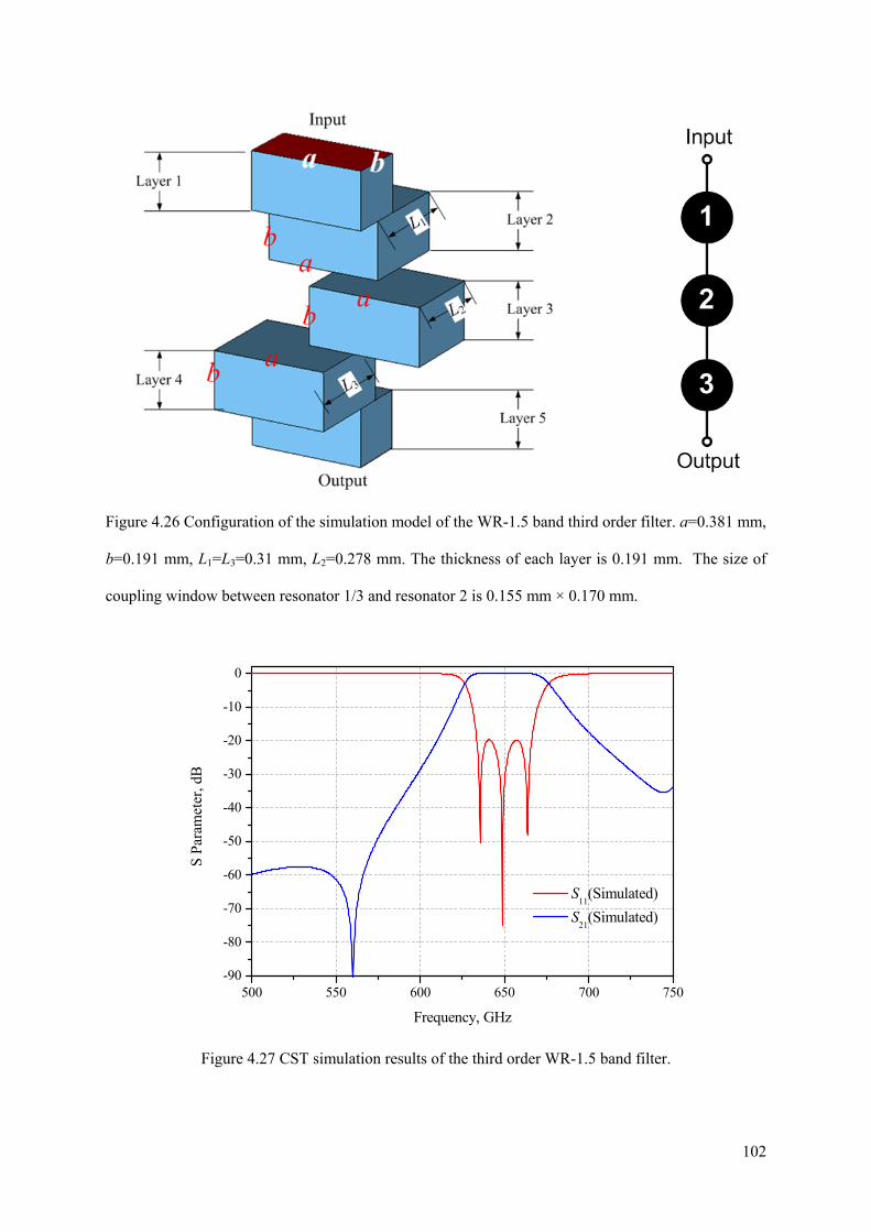
102
Figure 4.26 Configuration of the simulation model of the WR-1.5 band third order filter. a=0.381 mm,
b=0.191 mm, L1=L3=0.31 mm, L2=0.278 mm. The thickness of each layer is 0.191 mm. The size of
coupling window between resonator 1/3 and resonator 2 is 0.155 mm × 0.170 mm.
Figure 4.27 CST simulation results of the third order WR-1.5 band filter.
500 550 600 650 700 750-90
-80
-70
-60
-50
-40
-30
-20
-10
0
S P
aram
eter
, dB
Frequency, GHz
S11
(Simulated)
S21
(Simulated)

103
The simulation results of this filter are shown in Figure 4.27. As can be observed, there is an
unexpected transmission zero positioned at 560 GHz. This is due to the cancellation effect between
the signals transmitted through different paths from the input port to the output port. As shown in
Figure 4.28, after considering the cross coupling between resonators 1 and 3, the response obtained
from the calculated coupling matrix shows a good agreement with the simulation result.
Figure 4.28 The designed 3rd order WR-1.5 band filter’s S21 magnitude responses plotted using CST
simulation data (blue line) and the calculated coupling matrix (magenta line). For the calculation
model, a weak cross coupling m13 has been assumed and the rest coupling coefficients and external
quality factors are same as the specification.
During the measurement, the five layers of this WR-1.5 filter will be aligned using the pins from
flanges of the network analyzer. Then the screws from the flange will go through all five layers and fit
into the screw holes on the other flange. This will ensure a tight contact between all five SU-8 layers
as well as external flanges. Figure 4.29 shows two configurations of the third SU-8 layer and an
illustration of the measurement setup. This WR-1.5 band filter will be assembled and measured when
the measurement system is available.

104
Figure 4.29 (a) Configuration of the third layer of the WR-1.5 filter. (b) A photograph of the
fabricated third layer. (c) An illustration of the measurement setup for this WR-1.5 filter.
4.6 Conclusions
This chapter presents several SU-8 micromachined waveguide circuits with two integrated H-plane
back-to-back bends. These bends are employed to achieve a tight and accurate connection between the
micromachined circuits and external flanges from the network analyzer. Three kinds of bend
structures have been developed for the micromachined waveguides and filters operating at WR-10
band and WR-3 band. Both the separate SU-8 single-layer process and the joint two-layer process
have been employed to fabricate the WR-3 band waveguide circuits. Their measurement results have
been presented and compared.
References
[1] Li Y., Kirby P. L., Papapolymerou J.: ‘Silicon Micromachined W-Band Bandpass Filter Using
DRIE Technique,’ in Proc. 36th Eur. Microw. Conf., 2006, pp. 1271-1273.
[2] Sammoura F., Su Y.C., Cai Y., Chi C.Y.: ‘Plastic 95-GHz rectangular waveguides by Micro
Molding Technologies,’ Sens. Actuators A., Phys. 2006, 127, pp. 270-275.
[3] Sammoura F., Fuh Y.K., Lin L.: ‘Micromachined Plastic W-Band Bandpass Filters,’ Sens.
Actuators A., Phys. 2008, 147, pp. 47-51.

105
[4] Song S., Yoo C. S., Seo K. S.: ‘W-Band Bandpass Filter Using Micromachined Air-Cavity
Resonator with Current Probes,’ IEEE Microw. Wireless Components Lett. , 2010, 20, (4), pp. 205-
207.
[5] Chow W. H., Champion A., and Steenson D. P.: ‘Measurements to 320 GHz of millimetre-wave
waveguide components made by high precision and economic micro-machining techniques,’ High
Frequency Postgraduate Student Colloquium, 2003, pp. 90-93.
[6] Kerr A.R., Litton C., Petencin G., Koller D., and Shannon M.: ‘Loss of Gold plated Waveguides at
210-280 GHz’ ALMA MEMO 585, 2009, pp. 1-6
[7] Smith C. H., Barker N. S.: ‘SU-8 Micromachining Process for Millimeter and Submillimeter-
Wave Circuit Fabrication,’ in 33rd International Conf. on Infrared Millimeter and Terahertz Wave,
2008, pp. 1-2.
[8] Smith C. H., Sklavonuos A., Barker N. S.: ‘SU-8 Micromachining of Millimeter and
Submillimeter Waveguide Circuits,’ in IEEE MTT-S International, 2009, pp. 961-964.
[9] Stanec J. R. and Barker N. S., ‘Fabrication and Integration of Micromachined Millimeter-Wave
Circuits,’ IEEE Microw. and Wireless Component Letters, accepted for inclusion in the future issue of
this journal, according to IEEE explore
[10] Stanec J. R., Smith C. H., and Barker N. S., ‘Integrating Micromachined Circuits into
Submillimeter Systems,’ European Microwave Conference (EuMc), 2010, pp. 53-56
[11] CST Microwave Studio, CST GmbH, Darmstadt, Germany, 2006
[12] Kerr A.R.: ‘Elements for E-plane Split-Block Waveguide Circuits’, ALMA Memo 381
[13] http://www.home.agilent.com/upload/cmc_upload/All/Agilent_Waveguide_Overview1.pdf,
[14] Hong J., Lancaster M.J. ‘Microstrip filters for RF/microwave applications’ (John Wiley & Sons,
Inc, 2001)
[15] Alison W.B.W : ‘A handbook for the mechanical tolerancing of waveguide components’ (Artech
House, 1972)
[16] Ruiz-Cruz J. A., Zaki K. A., Montejo-Garai J. R. and Rebollar J. M.: ‘Rectangular waveguide
elliptic filters with capacitive and inductive irises and integrated coaxial excitation’, IEEE MTT-S Int.
Microw. Symp. Dig., Long Beach, CA, June 2005, pp. 269-272
[17] Rosenberg U., Amari S., and Bornemann J.: ‘Inline TM110- Mode filters with high-design
flexibility by utilizing bypass couplings of nonresonating TE10/01 modes’, IEEE Trans. Microw.
Theory Tech., 2003, 51, (6), pp. 1735-1742
[18] Craven G. F., Skedd R. F.: ‘Evanescent Mode Microwave Components’ (Artch House Inc., 1987)
[19] Skaik T., Wang Y., Ke M.L., Lancaster M.J.: ‘A Micromachined WR-3 Waveguide With
Embedded Bends for Direct Flange Connections,’ European Microw. Conf., Paris, 2010, pp.1225-
1228

106
Chapter 5
Micromachined Waveguide Circuits Measured with Block
Two different measurement methods for the SU-8 micromachined waveguide circuits are presented in
this thesis. The first one is achieved by using two micromachined H-plane back-to-back bends,
detailed in Chapter 4. The other one is accomplished by using a metal block, which is presented in
this chapter. This metal block measurement technology employs a conventionally machined metal
block, constructed from two separate pieces, in which to mount the micromachined circuits. A
waveguide choke flange has been adopted to eliminate the effect of air gap at the joints/interfaces
between the micromachined circuit and the metal block.
In this chapter Section 5.1 presents the general principles of the block measurement method. In
Section 5.2, the effect of the air gap at the interface between the micromachined device and the metal
block is investigated. Section 5.2 also includes a discussion of the photonic bandgap structure (PBG)
and the waveguide choke flange, both of which are proposed to address the problems caused by the
air gap at the joint. Section 5.3 describes the design and measurement performance of a straight
through waveguide and a 5th order Chebyshev filter obtained from the SU-8 single-layer fabrication
process. These two circuits have also been fabricated using the SU-8 two-layer process, and their
measurement performance is reported in Section 5.4. The WR-3 band eighth order dual-band filter,
described in Chapter 4, has been fabricated using the SU-8 two-layer process and measured using the
metal block technique. This dual-band filter is discussed in Section 5.4. In the final part of this chapter,
a conclusion is given in Section 5.5.
5.1 Principles of Block Measurement Method
In the work presented in this chapter, a conventional precision machined metal block comprised of
two separate pieces has been employed to mount the micromachined circuits, as illustrated in Figure
5.1.

107
Figure 5.1 (a) Overview of the measurement block, consisting of two separate pieces. Four screws are
employed to achieve intimate contact between Piece I and II. A plastic screw is introduced to
eliminate air gap between the micromachined circuit and Piece II. (b) Overview of the measurement
block (screw and pin holes are omitted for a clearer view). The micromachined circuit is also shown
(yellow). (c) Piece II of the metal block with half of the micromachined circuit. (d) Piece II of the
measure block. Four alignment pins are adopted for the alignment between the micromachined circuit
and the metal block. (e) A close up view of the micromachined circuit formed with four SU-8 layers.

108
The metal block is split along the E-plane of a WR-3 band waveguide so is in two separated pieces.
Four screws and four location pins across both pieces are used to provide an accurate and secure fit
between them. The micromachined circuits are placed in the middle of the block and standard WR-3
band waveguide flanges (i.e. UG-387) are connected to the block ends. The four alignment pins, as
illustrated in Figure 5.1 (d), address the accuracy to which the four SU-8 layers are aligned, as well as
the accuracy to which the micromachined circuit is aligned to Piece II of the metal block. A plastic
screw is utilised here to push the micromachined circuits towards Piece II.
The main advantages of this metal block measurement method are (i) the block can be used over and
over again on different WR-3 band micromachined SU-8 waveguide circuits; (ii) the loss of the metal
waveguide can be taken into consideration and removed through the use of a calibration metal block.
A shortcoming of this measurement approach is that it cannot avoid the air gap at the joints between
the SU-8 circuits and the metal block during assembling. This shortcoming can be overcome by
means of a waveguide choke flange or PBG structures at the interfaces/joints, as discussed in detail in
the following section.
5.2 Waveguide Choke Rings and PBG Connectors
Normally pins are used to align the circuits to the waveguide opening of the standard metal flange and
screws are used to ensure an intimate contact with them. However, for this configuration of measuring
micromachined devices, there is no convenient way to employ pins and screws to eliminate the air gap
at the interfaces between the micromachined circuit and the metal block. Therefore the existence of an
air gap between the micromachining circuit and the block is inevitable. To investigate the effect of the
air gap, CST simulations towards a simplified model, which only consists of an air gap at one
interface between the micromachined waveguide and the block, have been carried out. A gap of 25
μm at the interface has been assumed and the simulated S parameter responses are shown in Figure
5.2. It shows that without additional assistant structures, a 25 μm air gap at one interface would result
in a return loss higher than 17 dB and an insertion loss of 1.38 dB at some frequencies within the WR-

109
3 band. Obviously, the return loss and insertion loss will become worse if the discontinuity effects at
both interfaces are considered.
Figure 5.2 CST simulation results of a 25 µm air gap at the interface between the SU-8 waveguide
and the metal block for three different cases: with no assistant structures (i.e. only gap), with a choke
flange and with a photonic bandgap (PBG) structure.
5.2.1 Photonic bandgap structure
A photonic bandgap (PBG) structure has been investigated to mitigate the effects of the air gap. PBG
is a periodic distributed structure at the joint of waveguide connectors to suppress microwave fields
propagation and current flow in the joint over a wide frequency range [1]. The PBG structure is
capable of (i) significantly reducing the attenuation loss due to the discontinuities at the joints; (ii)
eliminating spectrally sharp features, caused by the presence of air gap at the interfaces, in the
circuit’s performance [1]. Normally PBG structure is periodically placed square pillars with a side
220 240 260 280 300 320
-40
-30
-20
-10
0
S P
aram
eter
, dB
S11(Only gap) S
21(Only gap)
S11
(Choke ring) S21
(Choke ring)
S11
(PBG) S21
(PBG)
Frequency, GHz

110
length and an interval of a quarter wavelength at the centre frequency. In [2] and [3], the basic
principle and theory of the PBG structure have been presented.
PBG structures have already been employed before to eliminate energy leakage in joints of waveguide
structures. In [1], experimental measurements toward an X-band waveguide are performed to
determine the effectiveness of the PBG structures. This straight through rectangular waveguide is split
along H-plane into two halves. PBG structures are machined on one surface of the joint to suppress
the current following into the joint. The measurement results show a remarkable reduction in the
waveguide loss using PBG structures against the same H-plane split waveguide without PBG
structures in the joint. Suggestions to the dimensions of the pillars (i.e. size, interval and height),
which offer the optimal performance, are given in [1]. Reference [4] reports a W-band waveguide
thermal isolator based on PBG structures. Excellent performance over the entire W-band has been
indicated by the simulation and measurement results of the thermal isolator. Reference [4] also states
that the gap between flanges with PBG structures can be as large as 3% of a wavelength without
seriously affecting the transmission and reflection responses throughout the whole W-band.
Additionally, by means of PBG structures, the thermal isolator becomes less sensitive to cocking and
misalignment during the connection [4].
In this work, CST simulations are carried out to determine the effectiveness of the photonic bandgap
structures. The PBG array is placed on the interface of the measurement metal block, whereas the
interface of the micromachined SU-8 circuit is flat, as shown in Figure 5.3. Due to the space
limitation at the interface of Piece II of the metal block, the pillars cannot be symmetrically placed.
According to CST simulations, this asymmetrical distribution has little effect on the performance of
the PBG array. Similar to the previous one, CST simulations are only performed on half of the metal
block with one through waveguide and the spacing between the pillars and the micromachined
waveguide is 25 µm. After CST optimisation, the size of pillars is chosen as d1 = d2 = w1 = w2 = 0.225
mm and the height of pillars h is selected as 0.075 mm. Their corresponding S parameter magnitude
responses can be found from Figure 5.2.
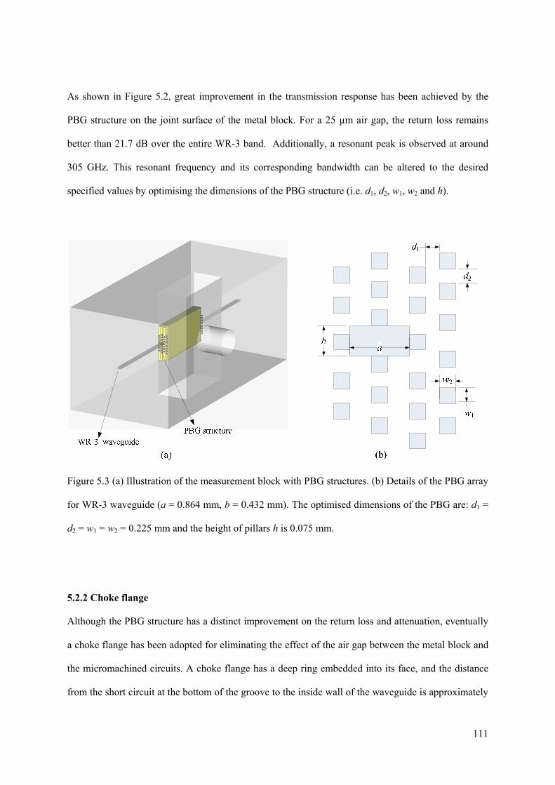
111
As shown in Figure 5.2, great improvement in the transmission response has been achieved by the
PBG structure on the joint surface of the metal block. For a 25 µm air gap, the return loss remains
better than 21.7 dB over the entire WR-3 band. Additionally, a resonant peak is observed at around
305 GHz. This resonant frequency and its corresponding bandwidth can be altered to the desired
specified values by optimising the dimensions of the PBG structure (i.e. d1, d2, w1, w2 and h).
Figure 5.3 (a) Illustration of the measurement block with PBG structures. (b) Details of the PBG array
for WR-3 waveguide (a = 0.864 mm, b = 0.432 mm). The optimised dimensions of the PBG are: d1 =
d2 = w1 = w2 = 0.225 mm and the height of pillars h is 0.075 mm.
5.2.2 Choke flange
Although the PBG structure has a distinct improvement on the return loss and attenuation, eventually
a choke flange has been adopted for eliminating the effect of the air gap between the metal block and
the micromachined circuits. A choke flange has a deep ring embedded into its face, and the distance
from the short circuit at the bottom of the groove to the inside wall of the waveguide is approximately
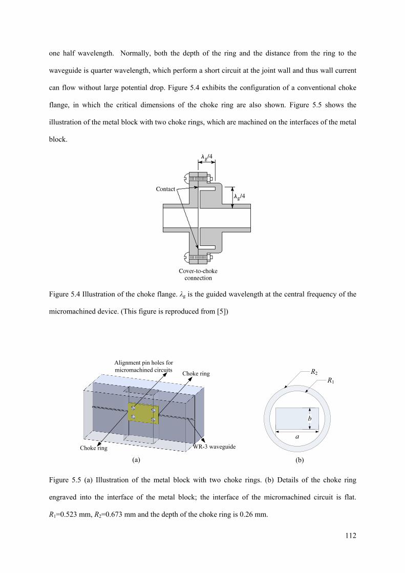
112
one half wavelength. Normally, both the depth of the ring and the distance from the ring to the
waveguide is quarter wavelength, which perform a short circuit at the joint wall and thus wall current
can flow without large potential drop. Figure 5.4 exhibits the configuration of a conventional choke
flange, in which the critical dimensions of the choke ring are also shown. Figure 5.5 shows the
illustration of the metal block with two choke rings, which are machined on the interfaces of the metal
block.
Figure 5.4 Illustration of the choke flange. λg is the guided wavelength at the central frequency of the
micromachined device. (This figure is reproduced from [5])
WR-3 waveguide
Choke ring
Alignment pin holes for micromachined circuits
(a) (b)
R1
R2
a
b
Choke ring
Figure 5.5 (a) Illustration of the metal block with two choke rings. (b) Details of the choke ring
engraved into the interface of the metal block; the interface of the micromachined circuit is flat.
R1=0.523 mm, R2=0.673 mm and the depth of the choke ring is 0.26 mm.
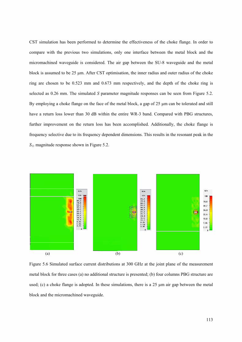
113
CST simulation has been performed to determine the effectiveness of the choke flange. In order to
compare with the previous two simulations, only one interface between the metal block and the
micromachined waveguide is considered. The air gap between the SU-8 waveguide and the metal
block is assumed to be 25 µm. After CST optimisation, the inner radius and outer radius of the choke
ring are chosen to be 0.523 mm and 0.673 mm respectively, and the depth of the choke ring is
selected as 0.26 mm. The simulated S parameter magnitude responses can be seen from Figure 5.2.
By employing a choke flange on the face of the metal block, a gap of 25 µm can be tolerated and still
have a return loss lower than 30 dB within the entire WR-3 band. Compared with PBG structures,
further improvement on the return loss has been accomplished. Additionally, the choke flange is
frequency selective due to its frequency dependent dimensions. This results in the resonant peak in the
S11 magnitude response shown in Figure 5.2.
(a) (b) (c)
Figure 5.6 Simulated surface current distributions at 300 GHz at the joint plane of the measurement
metal block for three cases (a) no additional structure is presented; (b) four columns PBG structure are
used; (c) a choke flange is adopted. In these simulations, there is a 25 µm air gap between the metal
block and the micromachined waveguide.
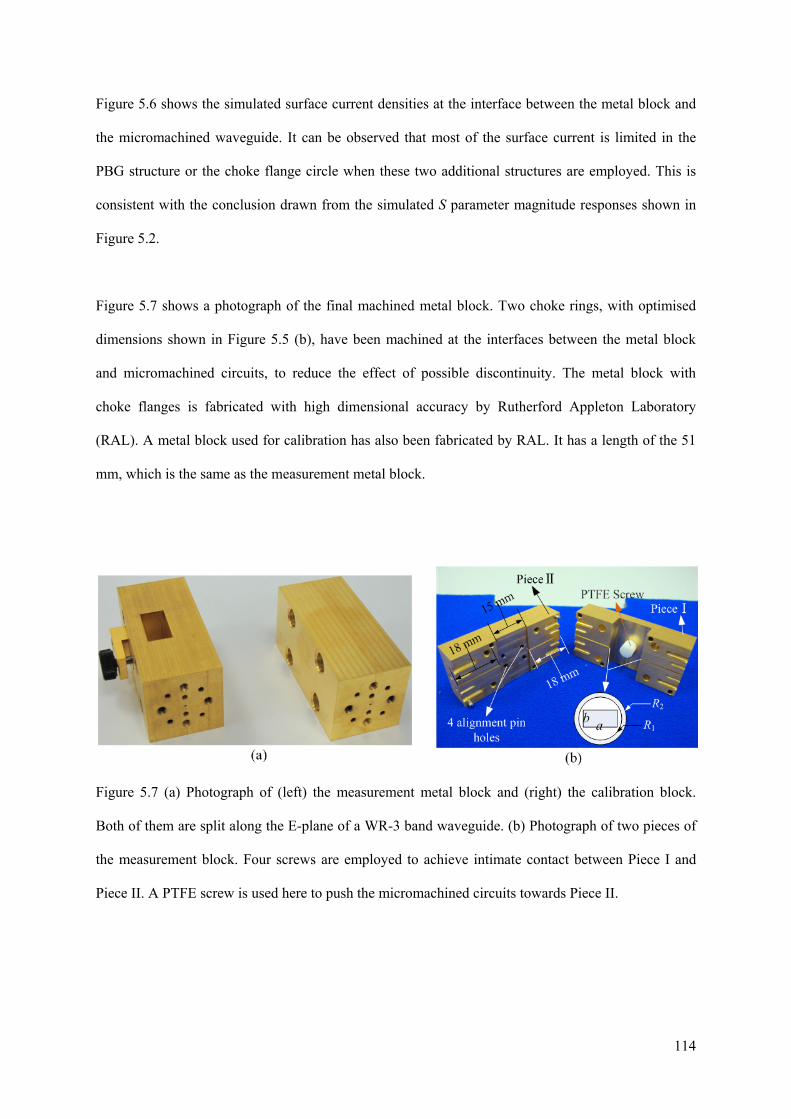
114
Figure 5.6 shows the simulated surface current densities at the interface between the metal block and
the micromachined waveguide. It can be observed that most of the surface current is limited in the
PBG structure or the choke flange circle when these two additional structures are employed. This is
consistent with the conclusion drawn from the simulated S parameter magnitude responses shown in
Figure 5.2.
Figure 5.7 shows a photograph of the final machined metal block. Two choke rings, with optimised
dimensions shown in Figure 5.5 (b), have been machined at the interfaces between the metal block
and micromachined circuits, to reduce the effect of possible discontinuity. The metal block with
choke flanges is fabricated with high dimensional accuracy by Rutherford Appleton Laboratory
(RAL). A metal block used for calibration has also been fabricated by RAL. It has a length of the 51
mm, which is the same as the measurement metal block.
Figure 5.7 (a) Photograph of (left) the measurement metal block and (right) the calibration block.
Both of them are split along the E-plane of a WR-3 band waveguide. (b) Photograph of two pieces of
the measurement block. Four screws are employed to achieve intimate contact between Piece I and
Piece II. A PTFE screw is used here to push the micromachined circuits towards Piece II.

115
5.3 WR-3 Band Circuits From SU-8 Single-Layer Process
5.3.1 WR-3 band through waveguide
Figure 5.8 Configuration of the layered WR-3 band through waveguide. (a) Illustration of the
structure which consists of four layers. The length of the waveguide L is 14.97 mm. Four alignment
pin holes are shown. (b) Front view of the micromachined waveguide, each layer has a thickness t of
0.432 mm. a=0.864 mm, b= 0.432 mm.
The micromachined WR-3 band straight through waveguide is comprised of four gold-coated SU-8
layers with a same thickness of 0.432 mm, as illustrated in Figure 5.8. These four layers are
fabricated using the SU-8 single-layer process. After obtaining the four separate SU-8 layers, the top
two layers (i.e. layer 1 and 2) are aligned and bonded on top of each other with silver loaded epoxy
around the edges. A second metal evaporation to the bonded layers is performed to minimize the
resistive loss and to avoid the effect of the possible air gaps. The same procedure is carried out for the
bottom two layers. It should be noted that a pair of temporary links through a tether structure is used
at the ends of the layer 2 or 3 in the fabrication procedure to fix the position of its two separate halves,
as shown in Figure 5.9. These links help hold the two halves in the alignment procedure, and are
removed after the bonding of layers 1 and 2, and layers 3 and 4.

116
Figure 5.9 Photograph of two SU-8 waveguide layers.
CST simulation results of this WR-3 waveguide are displayed in Figure 5.11. As mentioned before, a
conductivity of 1.86×10⁷ S/m has been employed here as the effective conductivity of
sputtered/evaporated gold outside the SU-8 layer. According to CST simulations, this equivalent
conductivity accounts for an average insertion loss of 0.4 dB for this 14.97 mm long straight through
waveguide, as shown in Figure 5.11.
Measurements are performed using an Agilent E8361A Network Analyzer with OML WR-3
extension modules subject to enhanced response calibrations. The metal calibration block with a
length of 51 mm is measured first and has an average insertion loss of 1 dB, corresponding to an
attenuation of 0.02 dB/mm, as shown in Figure 5.10. In this figure, the loss factor is included to
understand the source of loss in the calibration metal waveguide and it can be computed by [6]
2 2
11 21
2 2
10 11 21
Loss Factor(magnitude)
Loss Factor(dB) 20 log ( )
S S
S S
(5.1)
The loss factor for a lossless circuit will be 1.0 in magnitude or 0 in dB. Compared with insertion loss,
the loss factor is able to show the loss of the circuit more accurately since it also factors in the effect
of the return loss (i.e. S11). For a perfectly matched circuit, the loss factor is equal to the insertion loss.
Temporary links
Layer 1 or 4 Layer 2 or 3
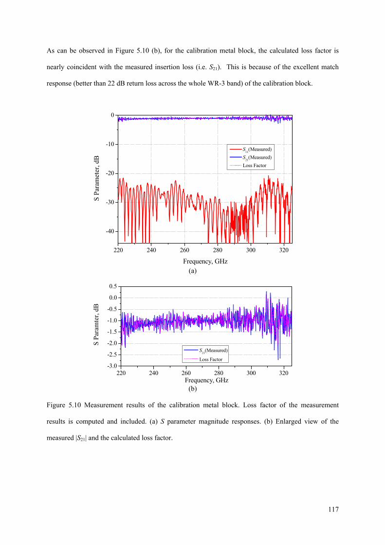
117
As can be observed in Figure 5.10 (b), for the calibration metal block, the calculated loss factor is
nearly coincident with the measured insertion loss (i.e. S21). This is because of the excellent match
response (better than 22 dB return loss across the whole WR-3 band) of the calibration block.
(a)
(b)
Figure 5.10 Measurement results of the calibration metal block. Loss factor of the measurement
results is computed and included. (a) S parameter magnitude responses. (b) Enlarged view of the
measured |S21| and the calculated loss factor.
220 240 260 280 300 320
-40
-30
-20
-10
0
S11
(Measured)
S21
(Measured)
Loss Factor
S P
aram
eter
, dB
Frequency, GHz
220 240 260 280 300 320-3.0
-2.5
-2.0
-1.5
-1.0
-0.5
0.0
0.5
S P
aram
ter,
dB
Frequency, GHz
S21
(Measured)
Loss Factor

118
For the measurement transmission responses of the micromachined waveguide circuits, the loss of the
36 mm long metal waveguide of the measurement block has been taken into consideration and
removed. It is accomplished by subtracting 36/51 of the loss factor (in dB) of the calibration block
from the SU-8 circuit’s measured S21 magnitude (in dB) results, at their corresponding frequency
points.
Figure 5.11 shows the measurement results of the 14.97 mm long micromachined SU-8 straight
through waveguide, in which an average insertion loss of 0.6 dB or 0.04 dB/mm and a return loss
better than 17 dB across the whole WR-3 band have been exhibited.
As described in Chapter 2, the waveguide (operating at TE10 mode) attenuation due to conductor loss
can be computed from the conductivity of the metal walls by
0
2 3 2 20 0
3 2 20 0 0 2
(2 4 ) 8.686 dB/m1
2 4c
f
b a f
a b f fa
(5.2)
where σ is the conductivity of the waveguide wall, a and b are waveguide dimensions, µ0 and ε0 are
the permeability and permittivity of free space, f is the operating frequency. As can be seen from
Figure 5.11 (a), the theoretical loss for σ=1.86×10⁷ S/m calculated by equation (5.2), agrees well with
the CST simulation result. Additionally, according to the theoretical loss calculation, an equivalent
conductivity of 7×10⁶ S/m gives the best fit to the measured insertion loss of the SU-8 through
waveguide.
It should be pointed out that, the length of the SU-8 waveguide is 14.97 mm. This leaves a 15 µm gap
at each interface between the SU-8 waveguide and the measurement metal block. This additional gap
relieved the SU-8 layers from bending during the very tightly fitting of the longer waveguide when
loading the micromachined waveguide. As discussed in Section 5.2.2, the choke rings at the interfaces

119
have the ability to reduce the effect of the 15 µm gap significantly. This has been verified by the SU-8
micromachined waveguide’s measurement results.
(a)
(b)
Figure 5.11 Measurement and simulation results of the 14.97 mm long SU-8 straight through
waveguide. (a) |S21| in dB. The best fitted measured insertion loss curve corresponds to a conductivity
σ of 7×10⁶ S/m. (b) |S11| in dB. A conductivity of 1.86 × 10⁷ S/m is employed in the CST simulation.
220 240 260 280 300 320-1.6
-1.4
-1.2
-1
-0.8
-0.6
-0.4
-0.2
0
0.2
Frequency, GHz
|S21
| , d
B
SimulatedMeasured
Calculated( = 1.86e7 S/m)Calculated( = 7.0 e6 S/m)
220 240 260 280 300 320
-110
-100
-90
-80
-70
-60
-50
-40
-30
-20
Frequency, GHz
|S11
| , d
B
SimulatedMeasured

120
5.3.2 WR-3 band single band filter
A 5th order Chebyshev filter with a ripple bandwidth of 9% centered at 300 GHz has been designed
following the approach described in Chapter 2. To meet the filter’s specifications, the external Q and
the coupling coefficients between resonators are calculated to be: Qext=10.793, k12=k45=0.078,
k23=k34=0.057. In order to be consistent with the direction of etching of this layered structure, all
capacitive coupling irises have been adopted here to provide the required external Q and coupling
coefficients. Full-wave modeling is carried out in CST, and Figure 5.12 illustrates the detailed
dimensions obtained after optimisation. The simulation results of this filter are shown in Figure 5.13.
It can be seen that relatively lower rejection has been revealed in the lower stop-band, which is due to
the characteristics of capacitive coupling irises, as discussed in Chapter 4. In order to provide bigger
coupling gaps between resonators, which facilitate the metal evaporation process, the irises have been
placed asymmetrically along the waveguide. This WR-3 waveguide filter has also been made of four
separated layers and then bonded, the first and second, and the third and fourth layer together to form
two halves. The length of this WR-3 band filter including the SU-8 connecting waveguide is designed
to be 14.97 mm.
Figure 5.12 A schematic side-view diagram of the fifth order iris coupled WR-3 filter. Drawing is not
to scale. Some critical dimensions of the filter: h1=0.178 mm, h2= 0.3 mm, h3=0.341 mm, L1=0.696
mm, L2=0.645 mm, L3=0.640 mm, t1=0.1 mm, t2=0.143 mm, b=0.432 mm.

121
Figure 5.13 Measurement and simulation results of the 5th order micromachined WR-3 band filter
with a length of 14.97 mm.
The measurement results of the micromachined WR-3 waveguide filter are shown in Figure 5.13,
which exhibits a 9.7% 3 dB fractional bandwidth at a central frequency of 298.5 GHz. The average
passband insertion loss is measured to be 2 dB and the return loss is better than 10 dB in the majority
of the passband. Compared with the simulated 3 dB bandwidth of 31.7 GHz centred at 299.3 GHz,
there is a 0.8 GHz centre frequency shift downwards and a 3 dB bandwidth reduction of 2.68 GHz.
It is worth mentioning that, due to the asymmetrical stopband performance of the designed filter, the
simulated 3 dB bandwidth center frequency is slightly shifted to 299.3 GHz from the designed ripple
bandwidth centre frequency of 300 GHz. Generally the measured performance of this filter agrees
well with simulations. It has been demonstrated that the unexpected bump between 296-298 GHz in
|S11| is due to the uneven pressure generated by the PTFE screw of the metal block. After inserting a 2
mm thick brass plate between the screw and the micromachined filter, the bump disappears
accompanied by a worse insertion loss which is believed to be a result of looser contact between layer
220 240 260 280 300 320-50
-40
-30
-20
-10
0
S11
(Simulated)
S21
(Simulated)
S11
(Measured)
S21
(Measured)
S P
aram
eter
, dB
Frequency , GHz

122
2 and layer 3. Time domain analyse (gating operation) has been employed to investigate the ripple of
the S11 magnitude response over the frequency range from 240 GHz to 260 GHz. It has been found
that these ripples are attributed to the mismatch inside the micromachined waveguide filter structure.
The dissipation of a Chebyshev bandpass filter designed from its low-pass prototype can be estimated
by [7]
A1
4.343 dBn
ci
i ui
L gFBWQ
(5.3)
where ∆LA is the insertion loss increase at the centre frequency of the filter, FBW is the fractional
bandwidth of the practical filter, Ωc (typically 1 rad/s) is the cut-off frequency of the low-pass
prototype, g is low-pass element values and Qu is the unload quality factor of the waveguide
resonators. All of the resonators of this filter are operating at the TE101 mode. By employing an
equivalent conductivity of 7×10⁶ S/m, obtained from the SU-8 through waveguide measurement
results as described in Section 5.3.1, Qu of each resonator can be calculated to be 547. Substitute these
data into equation (5.3) yields ∆LA= 0.57 dB. Additionally, there are two SU-8 waveguide sections
connecting at the ends of this filter. The total length of the two SU-8 waveguide sections is around 10
mm. This contributes 0.4 dB extra loss to the filter’s measured passband insertion loss. Therefore, the
expected passband insertion loss of this filter with two connecting waveguide sections is around 0.97
dB. The rest 1 dB loss is believed to be attributed to the radiation loss at the interface and the loss due
to the bonded layers (i.e. layers 1 and 2, or layers 3 and 4).
Equation (5.3) also demonstrates that the dissipative loss (in dB) is inversely proportional to (i) the
unloaded quality factor of the filter resonators; and (ii) the fractional bandwidth of the filter.
Additionally, according to equation (5.3), the passband dissipative loss is independent of the choice of
the practical bandpass filter’s centre frequency. However, given the same wall conductivity, the Qu of

123
the resonator varies with its operating frequency. Therefore, the dissipative loss of a bandpass filter is
still related to its operating centre frequency.
(a)
(b)
Figure 5.14 Theory calculated S Parameter responses of the 5th order WR-3 band filter for three
assumed conductivities, i.e. 1.86 × 10⁷ S/m, 7 × 10⁶ S/m and 6 × 10⁵ S/m. (a) S21 magnitude responses.
(b) S11 magnitude response.
As stated in [7], the decreased Qu will not only lead to an increased filter passband insertion loss, but
also result in a reduction in the filter’s fractional bandwidth. This can be observed in Figure 5.14. In
this figure, the filter responses are plotted at three conductivities, i.e. 1.86 × 10⁷ S/m, 7 × 10⁶ S/m and
6 × 10⁵ S/m, which are corresponding to the theoretical conductivity of the thin-film-gold, the
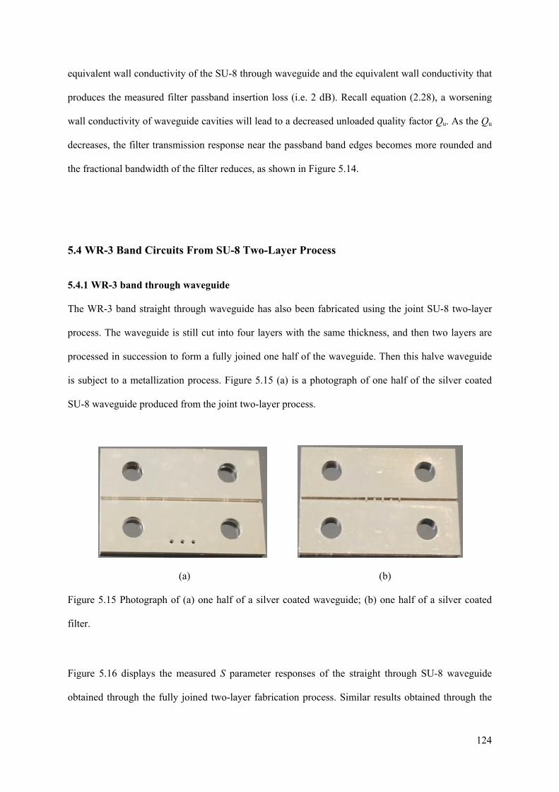
124
equivalent wall conductivity of the SU-8 through waveguide and the equivalent wall conductivity that
produces the measured filter passband insertion loss (i.e. 2 dB). Recall equation (2.28), a worsening
wall conductivity of waveguide cavities will lead to a decreased unloaded quality factor Qu. As the Qu
decreases, the filter transmission response near the passband band edges becomes more rounded and
the fractional bandwidth of the filter reduces, as shown in Figure 5.14.
5.4 WR-3 Band Circuits From SU-8 Two-Layer Process
5.4.1 WR-3 band through waveguide
The WR-3 band straight through waveguide has also been fabricated using the joint SU-8 two-layer
process. The waveguide is still cut into four layers with the same thickness, and then two layers are
processed in succession to form a fully joined one half of the waveguide. Then this halve waveguide
is subject to a metallization process. Figure 5.15 (a) is a photograph of one half of the silver coated
SU-8 waveguide produced from the joint two-layer process.
(a) (b)
Figure 5.15 Photograph of (a) one half of a silver coated waveguide; (b) one half of a silver coated
filter.
Figure 5.16 displays the measured S parameter responses of the straight through SU-8 waveguide
obtained through the fully joined two-layer fabrication process. Similar results obtained through the

125
separate single-layer process are also included for comparison. As shown in Figure 5.16 (b), the SU-8
waveguide from two-layer process shows an improvement in the insertion loss. This improved
insertion loss represents an average attenuation loss of 0.03 dB/mm, which is comparable to the
results of between 0.013 to 0.025 dB/mm obtained from the calibration metal block, as shown in
Figure 5.10. The measured return loss (i.e. |S11|) is better than 15 dB in majority of the WR-3 band.
The slightly worsened return loss is partially attributed to the improved insertion loss.
(a)
(b)
Figure 5.16 The measured S parameter magnitude performance (a) for the WR-3 waveguide with the
expanded view of |S21| shown in (b). The best fitted measured insertion loss curves of the SU-8
waveguides, obtained from the joint two-layer and the separate single-layer processes, correspond to a
conductivity σ of 1×10⁷ S/m and 7×10⁶ S/m, respectively.
220 240 260 280 300 320
-30
-20
-10
0
S11
(Two-Layer)
S21
(Two-Layer)
S11
(Single-Layer)
S21
(Single-Layer)
Frequency , GHz
S P
aram
eter
, dB
220 240 260 280 300 320-2.0
-1.5
-1.0
-0.5
0.0
0.5
|S21
| , d
B
Frequency , GHz
S21
(Two-Layer)
S21
(Single-Layer)
Calculated(=1e7 S/m) Calculated(=7e6 S/m)
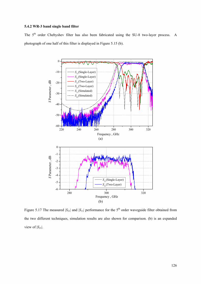
126
5.4.2 WR-3 band single band filter
The 5th order Chebyshev filter has also been fabricated using the SU-8 two-layer process. A
photograph of one half of this filter is displayed in Figure 5.15 (b).
(a)
(b)
Figure 5.17 The measured |S21| and |S11| performance for the 5th order waveguide filter obtained from
the two different techniques, simulation results are also shown for comparison. (b) is an expanded
view of |S21|.
220 240 260 280 300 320-60
-50
-40
-30
-20
-10
0
S11
(Single-Layer)
S21
(Single-Layer)
S11
(Two-Layer)
S21
(Two-Layer)
S11
(Simulated)
S21
(Simulated)
S Pa
ram
eter
, dB
Frequency , GHz
280 300 320-6
-5
-4
-3
-2
-1
0
S21
(Single-Layer)
S21
(Two-Layer)
S Pa
ram
eter
, dB
Frequency , GHz

127
Figure 5.17 displays the S parameter performance of the Chebyshev filter obtained from the two
different SU-8 fabrication techniques. The simulation responses are also included for comparison.
Both measured results exhibited a narrower-than-expected 3 dB bandwidth which is believed to be
due to the inaccuracies among the gaps of the coupling irises. The simulation results predicted a 3 dB
bandwidth of around 10.5%, while experimentally the results are 9.7% for separate single-layer
technique and about 8.2% for the joined two-layer one. The iris gaps is measured to be narrower than
designed by around 5% on average, this accounts for part of the observed narrowing (less than 0.5%)
according to CST simulations. The rest is likely due to the inaccuracies in other critical dimensions,
from the lengths of resonators to the width of the waveguide. The passband insertion loss improves
from an average of around 2 dB for the separate single-layer technique to about 1 dB for the joined
two-layer one. The return loss also shows an improvement for the joined two-layer device over the
separate single-layer one and is better than 12 dB within the passband. It is believed that the
improvements in both cases resulted from the fact that the two-layer technique produced more robust
coupling irises, where little movement is expected from them during the final bonding and assembly
stage, whereas in the separate single-layer case, the irises can move sideways when pressing them
together.

128
5.4.3 WR-3 band dual-band filter
The WR-3 band dual-band filter described in Chapter 4 has also been fabricated using the SU-8 two-
layer process and measured using the metal block measurement method. The configuration of the
dual-band filter is shown in Figure 5.18. As mentioned in Chapter 4, due to the two isolated features
within the circuit, this dual-band filter can only be fabricated using the joined two-layer process.
Figure 5.18 Configuration of the 8th order dual-band filter working at WR-3 band. a=0.864 mm,
b=0.432 mm, L=14.97 mm.
The measurement results of this dual-band filter are shown Figure 5.19. The measured filter centre
frequency has been shifted downward to around 275 GHz against the design/simulated 280 GHz. The
measured results exhibit an average passband insertion loss of around 4 dB and a passband return loss
below 10 dB. These measurement results are corresponding to the dual-band filter device produced
from the first attempt. It is believed that the second batch of the micromachined dual-band filter
would demonstrate a better measurement performance in terms of passband insertion loss and the
filter centre frequency.

129
(a)
(b)
Figure 5.19 Measured and simulated results of the WR-3 band dual-band filter with a length of 15 mm.
(a) S21 magnitude responses. (b) S11 magnitude responses. In this simulation, a conductivity of
1.86×10⁷ has been used.
5.5 Conclusions
This chapter explains the working principles of the metal block measurement technique. This is
followed by an introduction of the three WR-3 band micromachined waveguide circuits, which are a
straight through waveguide, a 5th order Chebyshev filter and an 8th order dual-band filter. Their
220 240 260 280 300 320-40
-30
-20
-10
0
|S11
| , d
B
Frequency , GHz
Simulated Measured
220 240 260 280 300 320-70
-60
-50
-40
-30
-20
-10
0
|S21
| , d
B
Frequency , GHz
Measured Simulated

130
measurement results are compared with their corresponding simulation results, and basically good
agreements have been shown by all these three circuits.
There is also a comparison between the results obtained from the two different SU-8 fabrication
processes, i.e. the separate single-layer process and the two-layer process. This comparison is also
performed in Chapter 4 for the WR-3 band waveguide circuits with bends. Basically, it can be
concluded that the joint SU-8 two-layer fabrication process produces a more robust device structures
which lead to an improved performance, especially for the filter device where the small iris structures
make the separate layer method less robust. This technique eliminates any possible air gaps between
the layer 1 and 2, or 3 and 4 due to inter-layer cross linking process. Additionally, this two-layer
fabrication technique is particularly suitable for devices consisting of isolated pieces/regions, such as
the dual band filter circuit presented in Section 5.4.3. Therefore, this SU-8 joint two-layer processing
technique provides extra flexibility in the circuit design procedure by allowing isolated features within
the circuits.
The devices presented in this thesis are designed to work in the frequency range of WR-3 band and
WR-10 band because of the availability of test equipment. The SU-8 fabrication techniques and these
two measurement techniques can be readily scaled to higher frequency ranges.
References
[1] Jeffrey Hesler: ‘A Photonic Crystal Joint (PCJ) for Metal Waveguides,’ IEEE MTT-s Digest,
pp.783-786, 2001.
[2] Matthaei G., Young L., and Jones E.M.T.:‘Microwave Filters, Impedance Matching Networks,
and Coupling Structures,’ (Norwood, MA, Artech House, Inc., 1980.)
[3] Joannopulous J.D., Winn R.N., ‘Photonic Crystals, Molding the Flow of Light,’ (Princeton NJ:
Princeton University, Press, 1995.)
[4] J.L. Hesler, A. R. Kerr and N. Horner: ‘A Broadband Waveguide Thermal Isolator,’ in 2003
International Symposium on Space THz Technology, Tucson AZ, April 2003.
[5] Pozar D.M.: ‘Microwave Engineering,’ (John Wiley & Sons, Inc., 2005)

131
[6] Sonnet User’s Manual, Release 12.54, Sonnet Soft Ware Inc.
[7] Hong J. S., Lancaster M. J. ‘Microstrip Filters for RF/Microwave Applications,’ (John Wiley &
Sons Inc., 2001)

132
Chapter 6
The Design of Multiple-Passband Filters using Coupling Matrix
Optimisation
6.1 Introduction
There are three available approaches to realize multi-passband frequency-selective circuits, as shown
in Figure 6.1. One way is to design N classical single-band bandpass filters and then connect them
together through input/output power splitter/combiner, as illustrated in Figure 6.1 (a). However, this
simple approach comes with a cost of overall circuit size and power loss due to the input-single
splitting process [1]. Figure 6.1 (b) shows the second approach which performs by introducing an
input multiplexer along with an output power adder. However, the wide-band power combiner and the
inter-module matching issues remain as shortcomings [1]. The third approach relies on designing a
single circuit realizing the multi-band characteristic, which is employed in the work presented in this
chapter. The advantage of the third approach is that it uses a single component incurring a lower mass
and volume and it also eliminates the need of inter-stage matching required by the other two schemes.
The superiority of the multi-band filter of the type in Figure 6.1 (c) has given impetus to the recent
development in design techniques, most of which are based on the coupling matrix theory. The cross-
coupled resonator filter is a popular choice in order to provide transmission zeros to divide the single
passband into multi-passband. The approach to calculate the coupling matrices for these cross-coupled
resonators filter specifications can be generally divided into two steps: (i) the synthesis of the
characteristic polynomials that fulfils the filter electrical specifications; (ii) the extraction of the
coupling matrix from these polynomials. These two steps will be discussed comprehensively later in
Sections 6.2 and 6.3. An implemented X-band (i.e. WR-90) dual-band waveguide filter is presented in
Section 6.4, which is followed by the conclusion part in Section 6.5.

133
Figure 6.1 Block diagrams of three multi-band bandpass frequency-selective circuit examples. (a)
Channelized filter network with input power splitter and output power combiner; (b) combine input
multiplex network with output power combiner; (c) multi-band filter circuit. [1]
6.2 Multi-Band Filter Polynomial Transfer Function Synthesis
This section describes the synthesis process for the characteristic polynomials to fulfil the multi-band
filters specifications. It is carried out by developing the polynomials for a lowpass multi-band
prototype filter (in the frequency domain Ω), which is normalized in terms of frequency, bandwidth
and impedance levels. This lowpass prototype retains the practical filter’s specifications, which are
typically defined by stopband attenuation levels, passband return loss levels, the locations and

134
fractional bandwidths of each passband and stopband. Figure 6.2 (a) illustrates S21 magnitude
response of an example lowpass prototype dual-band filter with two asymmetrical passbands at [-Ωc
Ωa] and [Ωb Ωc].
(a)
(b)
Figure 6.2 (a) S21 magnitude response of a lowpass prototype asymmetrical dual-band filter. Ωc
indicates the prototype filter’s angular cut-off frequency. In this work, Ωc has been assumed to be 1
rad /s. Ωa and Ωb are the band-edge frequencies of the first and second passband, respectively. (b) S21
magnitude response of the practical dual-band filter after lowpass-to-bandpass transformation.
135
Then the practical multi-band bandpass filter (in the frequency domain ω) over desired working centre
frequency (i.e. ω0) and bandwidth (i.e. ω2 - ω1) can be obtained by using the following lowpass-to-
bandpass transformation [2]:
0
0
( )c
s j jFBW
(6.1)
with
2 1
0
FBW
0 1 2 (6.2)
where FBW denotes the fractional bandwidth of the practical multi-band filter. It should be pointed
out that ω0 is slightly smaller than the centre of the passband calculated by (ω1+ω2)/2. For narrow
passband filter, these two values will roughly coincide with each other. Figure 6.2 (b) depicts the S21
magnitude response of the practical asymmetrical dual-band filter converted from its lowpass
prototype design shown in Figure 6.2 (a). It can be observed in Figure 6.2 that the passband and
stopband specifications are preserved during the lowpass-to-bandpass transformation.
Next, the synthesis of lowpass prototype filter’s characteristic polynomials will be explored. Note that,
in this work the prototype filter networks are assumed to be reciprocal (i.e. S21=S12), symmetric (i.e.
S11=S22) and lossless (i.e. |S11|2+|S21|
2=1). As mentioned previously in Chapter 2, a prototype filter’s
scattering parameters, S11(s) and S21(s), can be expressed in terms of the characteristic polynomials
F(s), E(s) and P(s) [3]:
11
( )( )
( )
F sS s
E s 21
( )( )
( )
P sS s
E s (6.3)
F(s) and E(s) are Nth-degree polynomials with highest-power coefficients equal to unity. P(s) has also
been normalized to its highest-power coefficient and its order is the same as the number of finite

136
transmission zeros. ε is the ripple constant of the multi-band filter which may be described in terms of
the characteristic polynomials and the prescribed return loss level in the ith passband, LRi,
R /10
1 ( )|
( )10 1bii s sL
P s
F s
(6.4)
where sbi is the passband band-edge frequency of the ith passband. From equation (6.3) it is readily
seen that the roots of P(s) and F(s) correspond to the filter’s transmission zeros (sTzP) and reflection
zeros (sRzP), respectively. The filter poles (sPP) common to S11(s) and S21(s) correspond to the roots of
E(s). After obtaining the positions of zeros and poles, the normalised polynomials can be determined
by the following equations.
TZ
TzP
1
( ) ( )N
i
P s s s
zPR
1
( ) ( )N
i
F s s s
(6.5)
PP
1
( ) ( )N
i
E s s s
where N is the order of the filter and NTZ is the number of finite transmission zeros (NTZ ≤ N-2).
Analytic techniques are already available for some well-known simple filters such as Chebyshev,
Butterworth and quasi-elliptic functions. Substantial work has been done to derive general
polynomial synthesis techniques for filters with arbitrary responses such as arbitrary distribution of
transmission zeros and/or equiripple passbands and stop-bands. Conventionally, by selecting the
required passband ripple and frequency locations of the transmissions zeros, recursive methods given
in [5] and [11] can be used to generate the polynomials for general Chebyshev single-band filters.
Polynomials of some dual and triple band filters can adopt the above two recursive methods using
frequency transformations [17-20], however, these methods are limited to dual- and triple-band filters

137
with fixed bandwidths and/or fixed positions of transmission zeros. In addition to these synthesis
techniques, optimisation on the positions of reflection zeros has been applied to produce the transfer
functions of dual-band filters [15-16]. In [24], an iterative method based on interpolation was
proposed to construct the polynomials for multi-passband filters with both symmetrical and
asymmetrical responses. However, convergence cannot be guaranteed when all parameters are
prescribed, this leads to an oversized problem, since the positions of transmission zeros, the order of
the filter, passband edge frequencies and the ripple levels of each passband are interdependent [25-26].
In this work, an iterative method for dual-band filter characteristic polynomials synthesis as reported
in [26] has been used to derive polynomials F(s) and P(s) for multi-band filters. This polynomial
synthesis procedure along with two examples is described in Appendix I.
After finding F(s) and P(s) using above iterative techniques, E(s) can be derived from the well-known
conservation of energy equation as follows:
* *11 11 21 21( ) ( ) ( ) ( ) 1S s S s S s S s or 2
1( ) ( ) ( ) ( ) ( ) ( )F s F s P s P s E s E s
(6.6)
where the star symbols superscript represent complex conjugate. By substituting F(s) and P(s) into
the left hand side of equation (6.6), the 2N roots of E(s)·E(s)* can be found. These roots are
symmetric about the imaginary axis of the complex s plane and the ones in the left half of the complex
plane correspond to the roots of E(s) (i.e. sPP), since E(s) is a strictly Hurwitz polynomial for lossless
passive circuit [3]. After obtaining the frequency locations of filter poles, equation (6.5) can be
applied to calculate polynomial E(s).
It is worth mentioning that there are a few rules associated with the distribution of zeros and poles of
multi-band filters, as summarized in the following [3]:
1. The roots of E(s) are in the left half of the complex plane, and they are symmetrical to the real
axis when the filter response is symmetrical (i.e. filter built from synchronously tuned

138
coupled resonators). These poles will not be symmetrical to real axis when the filter response
is asymmetrical (i.e. filter constructed with asynchronously tuned coupled resonators).
2. The roots of P(s) must lie on the imaginary axis or distributed symmetrically with respect to
the imaginary axis for physically realizable filter circuit [35]. Pure imaginary transmission
zeros, which are close to the passbands, are employed to offer improved selectivity or to
divide the single passband into multi-passband. Complex transmission zeros can be
introduced to provide group delay equalization.
3. The majority classes of filters for instance Chebyshev or Butterworth, the roots of F(s) will lie
on the imaginary axis. In this work, all the reflection zeros are assumed to be pure imaginary.
Complex reflection zeros have been adopted by certain specialized cases such as predistorted
filters [21], which are beyond the scope of this chapter.
As stated in equation (6.5), the characteristic polynomials can be directly formed using these zeros
and poles. Therefore, the above rules on positions of zeros and poles will lead to a few properties of
filter polynomials, as shown in the following.
1. For filters with symmetric responses, E(s) is a Nth degree polynomial with real coefficients.
For filters with asymmetrical responses, the coefficients of E(s) are complex values except
that the leading coefficient equals to one.
2. For symmetric filters, F(s) is an Nth degree even polynomial if N is even and odd polynomial
if N is odd. All the coefficients of F(s) are real if the filter response is symmetric. For
asymmetric filters, the coefficients of F(s) will change between purely real and purely
imaginary as the power of s increases [3].
3. P(s) is an NTZth degree polynomial, which has the same form as F(s), where NTZ is the number
of finite transmission zeros.
The group delay of the lowpass prototype filter could be entirely determined from the frequencies of
filter poles (i.e. sPP) using the following equation [3]:

139
LPF 2 2 2 21 1
Re( )
( ) ( )Re( ) Im( )
N Nk k
k k k kk k
d s
d s s
(6.7)
where sk=σk+jΩk represents the kth root of the E(s), Ω indicates the angular frequency. In this work,
the group delay is computed using above equation rather than by numerical derivative computation of
the S21 phase. Additionally, the group delay of the practical bandpass filter, which is transformed
from the lowpass prototype, can be derived as [3]
BPF LPF
d d d d
d d d d
(6.8)
Recall the lowpass-to-bandpass transformation equation (6.1), the above equation can be modified to
0BPF LPF 2
0
1( )c
FBW
Expand the expression of FBW to (ω2-ω1)/ω0 and assume a narrow fraction bandwidth (i.e. ω ≈ ω0),
resulting in [3]
0 0BPF LPF LPF2
2 1 0 2 1
1 2( )
( ) ( )c c
(6.9)
It can be observed from equation (6.9) that the bandpass filter group delay is directly related to its
absolute bandwidth and the group delay of its lowpass prototype filter, regardless of the chosen center
frequency.
6.3 Coupling Matrix Optimisation
After obtaining the characteristic polynomials of multi-band filter, attention is now focused on
generating the coupling matrix from these polynomials. The methods for deriving the coupling
matrices have been extensively explored such as [4-20] and these can be classified into two groups: (i)

140
methods based on direct synthesis combined with matrix rotations (i.e. similarity transformations)
[10-20], and (ii) methods based on optimisation of the coupling matrix [4-9]. Direct methods for one-
step coupling matrix synthesis are available for some special canonical topologies for instance the
wheel topologies [10], folded topologies [11], full topologies (i.e. all coupling coefficients are non-
zero) [11], and N+2 transversal network [12]. To achieve cascaded triplets and/or quadruplets from
the above canonical topologies, a sequence of matrix rotations is usually performed on the initial
coupling matrix. Unconstrained optimisation methods [13] or analytical methods [14] have been
introduced to determine the rotation angles of each rotation sequence. However, the above reported
studies involving coupling matrix rotations are tied to specific filter topologies. A general analytical
method of transferring the initial coupling matrix into arbitrary desired form is not available yet.
Optimisation, with iteration towards specifically specified non-zero elements of the coupling matrix,
is an alternative approach to extract the coupling matrix for filters with cross couplings of arbitrary
topologies. In this method, a cost function (i.e. fitness function) is evaluated at each iteration and a
gradient based algorithm is employed to seek the optimal set of coupling coefficients to fulfil the filter
specification. This optimisation based design technique allows easy control of the filter topology and
the signs and magnitudes of certain coupling elements which may benefit the physical implementation
[5-6]. This is the main reason for employing the optimisation approach to generate coupling matrix
for multiple-passband filters in this work.
6.3.1 Cost function for coupling matrix optimisation
It is clear that the efficiency of the cost function is critical to the success of optimisation approach
since the cost function is evaluated at each iteration. There are a wide range of available cost
functions, most of which are evaluating the values of the filter’s transfer functions at critical
frequencies such as reflection and transmission zeros and band edges, as reported in [4-9]. In [22], a
cost function which compares the eigenvalues of the coupling matrix and its principal sub-matrix was
reported; coupling matrices synthesis for high order pseudo-elliptical single band filters was
141
demonstrated in a few optimisation steps. In [23] a cost function, defined using locations of zeros and
poles, has been used in an EM simulation optimisation to acquire physical dimensions of Chebyshev
filters.
In this work, the cost function measures the difference of the frequency locations of reflection and
transmission zeros between the responses produced by the coupling matrix and by the ideal
polynomials, as given by:
TZ
RzM RzP TzM TzP2 2
1 1
( ) ( ) ( ) ( ) ( )N N
i i
C s i s i s i s i
x (6.10)
where sRzM and sTzM are the complex frequency locations of the reflection and transmission zeros
calculated from the coupling matrix, NTZ is the number of finite transmission zeros. The vector
variable x stands for the set of control variables at the current optimisation iteration, i.e. the coupling
coefficients. This cost function is a least-squares formulation which has the advantage of placing more
weight on larger errors than smaller ones. The ideal frequency locations of the zeros (i.e. sRzP and sTzP)
are obtained using the abovementioned polynomial iterative design procedure. The optimisation
algorithm works by iteratively changing the entries of the coupling matrix which leads to the change
in the reflection and transmission zeros, causing the cost function to decrease until it is within a
specified tolerance.
One advantage of the cost function (6.10) is that no weighing is required. In most of the previous
work, the cost function is obtained by calculating and comparing S11 and S21 produced by the current
coupling matrix at certain critical frequencies with the objective values [4-9]. However, to make the
cost function work for high order filters, an appropriate weight should be placed on S11 or S21 to
balance the discrepancy between the values of S11 at reflection zeros and S21 at transmission zeros [8].
An empirical weight has been given in [8] and used in [9] and obviously that one is not suitable for all
the possible cases. In this work, all the terms of the cost function compare the differences of

142
frequency locations, which are in the same order of magnitude. Therefore, a unity weight can be
placed for each term as depicted in equation (6.10).
Moreover, the cost function (6.10) is also efficient since the calculation of the reflection and
transmission zeros from coupling matrix can be done by extracting the eigenvalues of two matrixes
respectively, as described in the following section. Then the left computation in (6.10) is simple and
straightforward. However, to evaluate the cost functions in [4-9], complex matrix calculation needs to
be performed for each reflection zero and transmission zero which leads to a longer computing time.
In the following, the calculation of reflection and transmission zeros from the supplied coupling
matrix will be explored. As discussed earlier in Chapter 2, S parameters can be directly related to the
coupling matrix as follows [2]:
111
111
2(1 )
eS A
q
1
211
e1 eN
12
NS A
q q
(6.11)
where the matrix [A] is defined as:
[ ] [ ] [ ] [ ]A q s I j m (6.12)
Here [I] is the N×N unit matrix, [q] is the N×N matrix with all entries zero except for q11=1/qe1,
qNN=1/qeN, [m] is the coupling matrix, and s is the complex normalised frequency variable. Then the S
parameters can be rewritten as [8]:
1111
1
2 cof ([ ])(1 )
det([ ])e
AS
q A
121
e1 e
2 cof ([ ])
det([ ])
N
N
AS
Aq q
(6.13)

143
where det([A]) denotes the determinant of matrix [A] and cofmn([A]) is the cofactor of matrix [A]
obtained by removing its row m and column n and then taking the determinant of the resulting matrix
and multiplying (-1)m+n . By comparing equation (6.13) with equation (6.3), the characteristic
polynomials can be expressed as:
11
1
1
e1 e
2 cof ([ ( )])( ) det([ ( )])
( ) 2 cof ([ ( )])
( ) det([ ( )])
e
N
N
A sF s A s
q
P s A s
q q
E s A s
(6.14)
Then the coefficients of these polynomials can be expressed in terms of the normalised external
quality factors and the coupling coefficients. The roots of these three polynomials correspond to sRzM
(reflection zeros calculated from coupling matrix), sTzM (transmission zeros calculated from coupling
matrix) and sPM (filter poles calculated from coupling matrix), respectively.
As equation (6.14) is not explicitly a polynomial form, an eigenvalue method is used to find the roots
(the calculated critical frequencies). The eigenvalues of a matrix [T] are precisely the solutions λ to
the characteristic equation det([T]- λ[I])=0. This calculation can be performed using the MATLAB
function eig([T]), which will return a vector of the eigenvalues of matrix T [28]. It should be noted
that, the function eig([T],[B]) in MATLAB, is able to compute generalized eigenvalues λ of a matrix
[T], which are the solutions to equation det([T]- λ[B])=0. This generalized eigenvalues calculation
function has been employed in the filter’s zeros calculation, as discussed later. If equation (6.12) is
rewritten as
[ ] [ ] ( [ ] [ ]) [ ] [ ']A s I j m q s I M (6.15)
From equations (6.14) and (6.15), it can been seen that the roots of E(s) are the eigenvalues of the
matrix [M´]. Similarly the roots of P(s) are directly related to the roots of cof1N([A(s)], which are the
generalized eigenvalues of matrix [ M´´] determined by

144
det( [ '] [ '']) 0s I M (6.16)
where [ M´´] and [ I´ ] are obtained by deleting the first row and last column of matrix [M´] and [ I ],
respectively.
In contrast to the expressions of P(s) and E(s), polynomial F(s) is formed with two individual parts, as
shown in equation (6.14). The roots of F(s) are acquired in three steps: (i) extract the roots of
cof11([A(s)]) using the above generalized eigenvalues calculation method; (ii) transform cof11([A(s)])
to a polynomial form from the roots obtained in (i) by means of a function poly(roots) in MATLAB;
(iii) subtract the coefficients of 2cof11([A(s)])/qe1 from the coefficients of det([A(s)]), and then
compute the roots of the resulting polynomial coefficients (i.e. sRzM) using a function roots(coefficient)
in MATLAB.
Up to now, all the locations of zeros and poles have been calculated using the set of coupling
coefficients at current iteration. Then these computed zeros will be compared with the desired
frequency locations using cost function (6.10). The corresponding cost, which indicates the fitness of
this set of coupling coefficients, will be evaluated to direct the following optimisation operations (i.e.
jump to the next iteration or return this set of value).
6.3.2 Calculation of external quality factor
In this work, the two external quality factors (i.e. qe1, qeN) are assumed to have the same value and are
calculated directly. In [27] an equation has been given to calculate qe from normalized characteristic
polynomial E(s), however, that equation is limited to filters with symmetrical responses (i.e. without
self-couplings). Here this equation has been extended to a more general form which includes filters
with asymmetrical responses (i.e. filters with self-couplings). After expanding the expression for E(s)
in equation (6.14) using elements of the coupling matrix, it is readily found that:

145
Coefficient of 1Ns term of E(s) =
11 22
e1 e
1 1( ... )NN
Nj m m m
q q (6.17)
Therefore the external quality factors can be determined from the real part of the second highest
coefficient of E(s) which was generated in the polynomial synthesis procedure. The negative
imaginary part of the coefficient of sN-1 equals to the sum of all self-couplings. In the case of
symmetric filter, all the resonators are resonating at the same frequency (i.e. all the self-couplings are
zero), then equation (6.17) can be simplified to 1/qe1+1/qeN=coefficient of sN-1 term of E(s), which has
the same form as the one reported in [27].
6.3.3 Coupling matrix optimisation flowchart
The majority reported coupling matrix optimisation work [4-8] employ a local optimisation algorithm,
the convergence of which depends highly on the quality of the supplied initial value. The best solution
may not be returned if the initial value is not adequately close to the global minimum. A genetic
algorithm (GA), which is operating by emulating the evolutionary process, is able to solve this
problem by virtue of its global optimisation capability. In most cases, the global optimum will be
found by GA optimisation given sufficient iterations. The GA also maintains its diversity in the search
procedure. However, in some cases the genetic algorithm may be considered inefficient, as it suffers
from slow convergence and may lack accuracy in the final solution [9]. This shortcoming can be
overcome by combining a GA with a gradient based local search algorithm such as sequential
quadratic programming (SQP), since the GA is able to provide strong initial values for the following
local optimisation. This hybrid technique has been applied successfully to coupling matrix synthesis
of a 10th order symmetrical dual-band filter and a 7th order asymmetrical single band filter in [9].
Figure 6.3 illustrates the flowchart of the hybrid optimisation technique.
In order to achieve the best performance of GA, different options should be experimented through
trial and error. The following describes some important parameters of GA, which may be altered to
improve optimisation results, as:

146
1. Initial values (i.e. initial population): GA does not require initial values and normally it
creates a random initial population with a uniform distribution in the feasible region. An
initial range of the population, which specifies the lower and upper bounds of each individual
in the initial population, can be set to reduce the algorithm running time if the approximate
values of the control variables are known. In this work, GA has generated the initial
population without supplying specified initial range of the population.
2. Population size: This specifies the size of individuals at each generation. Increasing the
population size will offer a better-fitted result at the cost of longer computing time, since
larger population size will enable the GA to search the solution space more thoroughly. It is
found that for the coupling matrix optimisation work presented in this chapter, a population
size, which is around 3~4 times the number of control variables, will return adequate results
for the following SQP search without taking a prohibitive amount of time.
3. Generation: This determines the maximum number of iterations the genetic algorithm runs
will perform. It acts as one of the most important Stopping Criteria options of GA. Increasing
the generations will produce a better final result.
4. Elite count: This indicates the number of individuals that will contribute to the population at
the next generation. These selected individuals (i.e. elite children) have the best fitness values
in the current generation. Setting Elite count to a high value will lead to the fittest individuals
to dominate the population, which will reduce the search efficiency. In this wok, elite count
has been set to two, as suggested in [29].
5. Crossover fraction: This denotes the fraction of the population created by crossover at the
next generation, not including elite children. Crossover children are formed by extracting the
best genes from different individuals and recombined them into potentially better-quality
children.
6. Mutation fraction: This specifies the fraction of individuals in each subpopulation that
migrates to a different subpopulation. Mutation ensures the diversity of population by adding
new random genes into the entries of the parent. Crossover and mutation are two critical
processes of GA. They are working together to produce new genes (by mutation) and
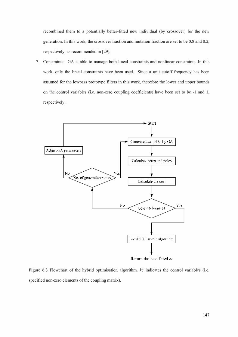
147
recombined them to a potentially better-fitted new individual (by crossover) for the new
generation. In this work, the crossover fraction and mutation fraction are set to be 0.8 and 0.2,
respectively, as recommended in [29].
7. Constraints: GA is able to manage both lineal constraints and nonlinear constraints. In this
work, only the lineal constraints have been used. Since a unit cutoff frequency has been
assumed for the lowpass prototype filters in this work, therefore the lower and upper bounds
on the control variables (i.e. non-zero coupling coefficients) have been set to be -1 and 1,
respectively.
Figure 6.3 Flowchart of the hybrid optimisation algorithm. kc indicates the control variables (i.e.
specified non-zero elements of the coupling matrix).

148
After obtaining the strong initial values using GA search, a local optimisation search function
‘fmincon’, is applied to seek the local minimum of the objective function(i.e. cost function) near the
starting point(i.e. initial values) in the feasible region defined through the constraints. ‘fmincon’ is a
gradient-based search method, which uses the second derivatives of the objective function to direct
the search for the minimum, and is available in Matlab optimisation toolbox. It is designed to find
minimum of constrained nonlinear multivariable objective functions and has been proved to be
effective in the field of nonlinear optimisation [37]. Since no analytical equation for the gradient of
the cost function has been provided in this work, ‘fmincon’ is working by estimating gradients via
finite differences calculation. This ‘fmincon’ search method is highly efficient and will normally
converge to the desired global minimum, because of the high quality initial values provided by GA.
It should be noted that GA is not gradient-based and it uses random number generators to produce the
next population.
6.3.4 Examples of coupling matrix optimisation
The above efficient cost function combined with the hybrid optimisation technique enable us to derive
coupling matrix for filters with complex responses and arbitrary desired topologies. In the following,
the capacity of this synthesis approach is demonstrated using four exemplar filters with increasing
complexity in terms of the order, topology, number of transmission zeros and number of passbands.
6.3.4.1 Example-A: Dual-Band filter with improved group delay
A 10th order asymmetrical dual-band filter with different passband return loss levels (LR1=20 dB,
LR2=40 dB) is illustrated as the first example. Three transmission zeros are placed at j0.205, j0.3,
j0.385 on the imaginary axis to produce two asymmetrical passbands located at [-j1, j0] and [j0.6, j1],
and the other pure imaginary transmission zero - j1.2 is used to provide a better rejection level on the
lower side of the passband. A complex pair of transmission zeros are placed at ± 0.4- j0.5 to offer

149
group delay equalization for the left passband. Using the iterative technique described in Section 6.2,
reflection zeros (sRzP) and filter poles (sPP) can be determined and then the filter polynomials are able
to be constructed. Table-6.1 illustrates the positions of zeros and poles after polynomials synthesis.
Their corresponding normalized characteristic polynomials F(s), E(s) and P(s) are calculated using
equation (6.5) and listed in Table-6.2.
Table-6.1 Zeros and poles locations of Example-A
TZs RZs Poles
-j 1.2 - j 0.9852 -0.0529 -j 1.0407
-0.4 –j 0.5 -j 0.8630 -0.1866 - j 0.9154
0.4 –j 0.5 -j 0.6460 -0.2308 - j 0.6448
j 0.205 -j 0.4063 -0.2312 -j 0.4172
j 0.3 -j 0.1656 -0.2413 - j 0.1152
j 0.385 -j 0.0176 -0.0590 + j 0.0494
j 0.6102 -0.0517 +j 0.5005
j 0.6943 -0.2276 + j 0.5274
j 0.8489 -0.4194+ j 0.8754
j 0.9803 -0.1952 + j 1.2306
Table-6.2 Normalised polynomial coefficients of Example-A
sn, n= P(s) F(s) E(s)
0 0.0116 -0.0002 0.0022-j 0.0005
1 j 0.0878 j 0.0146 0.0405+j 0.0062
2 -0.0779 0.0898 0.2451+j 0.0251
3 j 0.4015 j 0.0536 0.7896+j 0.1328
4 0.0921 0.7329 2.0385+j 0.3246
5 j 1.3100 j 0.0259 3.4199+j 0.5495
6 1 2.0759 5.0749+j 0.6166
7 -j 0.0632 4.7539+j 0.3344
8 2.4295 4.2264+j 0.1622
9 -j 0.0501 1.8958-j 0.0501
10 1 1
150
As shown in Table-6.2, the coefficients of E(s) are complex and those of F(s) and P(s) are changing
between pure real and purely imaginary as the power of s increases. These properties are due to the
asymmetrically located reflection and transmission zeros, as discussed in Section 6.2.
As stated in Section 6.3.2, the external quality factor is related to the second highest coefficient of
polynomial E(s), which has been highlighted in Table-6.2, via equation (6.17) as 2/qe1 =1.8958, after
rearranging this yields the external quality factor qe1=1.055.
A topology which cannot be synthesised directly has been chosen here for demonstration and is
shown in Figure 6.4. It should be noted that, the maximum number of transmission zeros for a given
coupling topology, can be determined by a simple rule:
The maximum number of finite transmission zero of a topology = N-Ns
where N is the degree of the filter and Ns is the number of resonators of the shortest path from the
input to the output port [3]. For this example, the shortest path is passing through four resonators (i.e.
1-4-7-10), therefore, the maximum number of accommodate transmission zeros is ten minus four,
which yields six. This rule can be employed to help the designer to select the proper topologies for
specified filter specifications. However, this shortest-path rule does not necessarily mean the
maximum number of transmission zeros is always achievable, since it also depends on the couplings
along other paths.
Optimisation is performed to obtain the corresponding coupling matrix and the final result is listed in
Table-6.3. Note that, the sum of all the self-couplings (i.e. m11, m22, m33, etc) in Table-6.3 equal to
0.0501, the negative of which coincides with the imaginary part of the second highest coefficient of
E(s), as listed in Table-6.2. This agreement is consistent with equation (6.17). Figure 6.5 (a) and (c)
show the responses (transmission/reflection loss and group delay) associated with the final coupling
matrix, as indicated as Case 1. In order to look into the effect of these two complex transmission zeros

151
(i.e. ± 0.4- j0.5) on the group delay, Case 2 which consists of six imaginary transmission zeros has
been considered and computed, as shown in Figure 6.5 (b). Case 1 and Case 2 have the same
bandwidths, passband return loss levels and the middle stopband rejection level. It should be pointed
out that another case, which has exactly the same magnitude responses as Case 1, is impossible to be
obtained because of the different positions of transmission zeros. With respect to S parameter
magnitude responses, Case 2 has been presented here as a very close representation of Case 1. As
shown in Figure 6.5 (c), by introducing a pair of complex transmission zeros at ± 0.4- j0.5, the group
delay variation of the left passband has been reduced.
Figure 6.4 Topology of Example-A
Table-6.3 Coupling matrix of Example-A
0.1357 -0.6232 -0.4024 -0.5083 0 0 0 0 0 0
-0.6232 -0.0280 0.5753 0 0 0 0 0 0 0
-0.4024 0.5753 0.1783 -0.3619 0 0 0 0.5093 0 0
-0.5083 0 -0.3619 -0.2984 0.4653 0 0.0599 0 0 0
0 0 0 0.4653 -0.1053 -0.0640 0 0 0 0
0 0 0 0 -0.0640 -0.0121 0.3198 0 0 0
0 0 0 0.0599 0 0.3198 -0.3412 0.5129 0 0.8137
0 0 0.5093 0 0 0 0.5129 -0.0287 -0.4145 0.3821
0 0 0 0 0 0 0 -0.4145 0.4141 0.0242
0 0 0 0 0 0 0.8137 0.3821 0.0242 0.1357
qe1=qe10=1.055

152
(a)
(b)
(c)
Figure 6.5 Computed responses of Example-A: (a) S parameter magnitude responses in dB of Case 1;
(b) S parameter magnitude response in dB of Case 2; (c) comparison between group delay responses
of Case 1 and Case 2.
Case 1: Transmission zeros= [ -0.4-j0.5 0.4-j0.5 -j1.2 j0.205 j0.3 j0.385 ];
Case 2: Transmission zeros= [ -j1.32 -j1.3 -j1.2 j0.205 j0.3 j0.385 ];
-2 -1.5 -1 -0.5 0 0.5 1 1.5 2-60
-50
-40
-30
-20
-10
0
Prototype Frequency, rad/s
S P
ara
met
er,
dB
S11(Case 1)S21(Case 1)
-2 -1.5 -1 -0.5 0 0.5 1 1.5 2-120
-100
-80
-60
-40
-20
0
Prototype Frequency, rad/s
S P
ara
met
er,
dB
S11(Case 2)
S21(Case 2)
-2 -1.5 -1 -0.5 0 0.5 1 1.5 20
5
10
15
20
25
30
35
40
45
50
Prototype Frequency, rad/s
Gro
up D
ela
y, s
Case 1Case 2
153
As discussed in Chapter 2, there is a trade-off between the filter’s selectivity in transmission response
and its group delay. In the case such as digital communication systems where a flat group delay is
essential, improved group delay can be achieved by introducing complex transmission zeros at the
expense of decreased stopband rejection. The effect of complex transmission zeros on group delay can
be adjusted by altering the real and imaginary parts of the complex transmission zeros.
6.3.4.2 Example-B: Dual-Band filter with wide middle stop-band
The abovementioned design approach is also capable of acquiring coupling matrices for filters with a
wide middle stopband. To demonstrate this, the following example is considered: an eighth order
asymmetrical filter with two passbands located at [-j1, - j 0.5] and [j0.65 j1]. Four transmission zeros,
which are located at -j0.4, -j0.22, j0.39, j0.55, have been employed to produce a wide stopband in the
middle passband. Two outside transmission zeros at -j1.6 and j1.35 are introduced to provide
increased selectivity in the near-out-of-passband region at the cost of lower attenuation in the far-out-
of-passband region. In this example, the return loss of the first passband is designed to be 20 dB and
the return loss of the second passband is calculated to be 25 dB.
The folded topology as shown in Figure 6.6 (a) has been adopted here to achieve the required
couplings. This kind of topology is popular and has two major advantages: (i) the maximum (N-2)
number of finite transmission zeros is feasible if necessary; (ii) it can be implemented easily, even the
diagonal couplings exist [3]. Figure 6.6 (b) shows a possible physical realization in coupled coaxial
resonator cavities for the filter topology in Figure 6.6 (a). Application of the design technique
described in the previous sections yields the coupling matrix that fulfils the desired specification, as
listed in Table-6.4. The external quality factor is calculated to be 2.0308. Their corresponding S
parameter responses are shown in Figure 6.7.
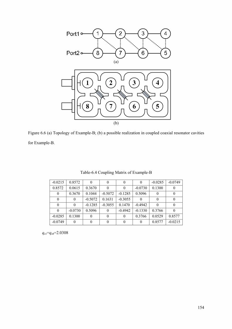
154
(a)
(b)
Figure 6.6 (a) Topology of Example-B; (b) a possible realization in coupled coaxial resonator cavities
for Example-B.
Table-6.4 Coupling Matrix of Example-B
-0.0215 0.8572 0 0 0 0 -0.0285 -0.0749
0.8572 0.0615 0.3670 0 0 -0.0730 0.1300 0
0 0.3670 0.1044 -0.5072 -0.1285 0.5096 0 0
0 0 -0.5072 0.1631 -0.3055 0 0 0
0 0 -0.1285 -0.3055 0.1470 -0.4942 0 0
0 -0.0730 0.5096 0 -0.4942 -0.1330 0.3766 0
-0.0285 0.1300 0 0 0 0.3766 0.0529 0.8577
-0.0749 0 0 0 0 0 0.8577 -0.0215
qe1=qe8=2.0308

155
Figure 6.7 Computed responses of Example-B
6.3.4.3 Example-C: Triple-Band filter with one notch stop-band
By placing two closer transmission zeros, notch stop-band can be produced for multi-band filters, as
depicted in the following Example-C. In this example, the three passband are located at [-j1 -j0.2], [j0
j0.46] and [j0.865 j1] and their passband return loss levels are LR1=20 dB, LR2=25 dB, LR3=30 dB. A
notch stopband has been produced by placing two close transmission zeros at -j0.102 and -j0.098
between the first and second passband. The other three transmission zeros at j0.61, j0.66 and j0.71
are introduced to separate the second and third passband.
The chosen topology is forming by cascading two quartets and a trisection, as shown in Figure 6.8 (a).
This topology can be realized either using the abovementioned coaxial resonator cavity resonators or
using shifted rectangular waveguide cavity resonators [38], as depicted in Figure 6.8 (b). After
optimisation, the resulting coupling matrix together with the calculated external quality factor is listed
in Table-6.5.
-2 -1 0 1 2-70
-60
-50
-40
-30
-20
-10
0
Prototype Frequency, rad/s
S P
ara
met
er,
dB
S11S21

156
(a)
(b)
Figure 6.8 (a) Topology of Example-C; (b) a possible realization in shifted rectangular waveguide
cavity resonators for Example-C.
Table-6.5 Coupling matrix of Example-C
-0.0845 -0.3474 0 -0.6924 0 0 0 0 0 0 0 -0.3474 0.3107 0.4320 0.0792 0 0 0 0 0 0 0
0 0.4320 0.3410 0.1137 0 0 0 0 0 0 0 -0.6924 0.0792 0.1137 -0.1393 0.5483 0 0 0 0 0 0
0 0 0 0.5483 -0.0476 -0.3207 -0.4904 0 0 0 0 0 0 0 0 -0.3207 0.6964 0.0557 0 0 0 0 0 0 0 0 -0.4904 0.0557 -0.1529 -0.5629 0 0 0 0 0 0 0 0 0 -0.5629 0.0073 0.2922 -0.0290 -0.7324 0 0 0 0 0 0 0 0.2922 0.6097 -0.1028 0 0 0 0 0 0 0 0 -0.0290 -0.1028 -0.0917 0.2522 0 0 0 0 0 0 0 -0.7324 0 0.2522 -0.0845
qe1=qe11=1.2162
The S parameter magnitude responses, associated with the above coupling matrix and external quality
factors, are exhibited in Figure 6.9. It is shown that a notch stopband has been achieved between the
first and second passband. Note that, the locations of this notch stoband can be easily adjusted by
altering the positions of its corresponding two transmission zeros.

157
Figure 6.9 Computed responses of Example-C
6.3.4.4 Example-D: Symmetrical Quad-Band Filter
By applying the same design approach, a 16th order quad-band filter with a symmetric response and a
compact topology, as shown in Figure 6.10, is demonstrated. This topology can be physically
implemented easily using for instance rectangular waveguide cavity resonators. The four
symmetrically located passbands of the filter are ± [j0.6, j1] and ± [j0.15, j0.3]. The return loss level
of the first and fourth passbands are designed to be 20 dB, and the return loss of the second and third
passbands are obtained as 30 dB, after the polynomials iterations synthesis. Twelve pure imaginary
transmission zeros are positioned at: ± j0.035, ± j0.075, ± j0.405, ± j0.45, ± j0.495, ± j1.5 to separate
different passbands.
After coupling matrix optimisation the resultant coupling coefficients (non-zero values) and
calculated external quality factors are shown below with their corresponding responses at normalized
frequency, which are given in Figure 6.11. Since this filter’s responses are symmetrical to the
prototype centre frequency, so there are no self-couplings in the coupling matrix.
-2 -1 0 1 2-60
-50
-40
-30
-20
-10
0
Prototype Frequency, rad/s
S P
ara
met
er,
dB
S11S21
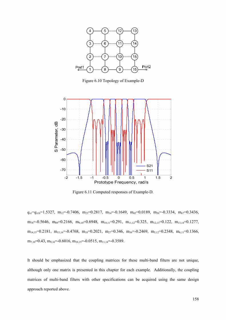
158
Figure 6.10 Topology of Example-D
Figure 6.11 Computed responses of Example-D.
qe1=qe16=1.5327, m12=-0.7406, m23=0.2817, m34=-0.1649, m45=0.0189, m56=-0.3334, m67=0.3436,
m78=-0.5646, m89=0.2166, m9,10=0.6948, m10,11=0.291, m11,12=0.325, m12,13=0.122, m13,14=0.1277,
m14,15=0.2181, m15,16=-0.4768, m18=0.2021, m27=0.346, m36=-0.2469, m5,12=0.2348, m6,11=0.1366,
m7,10=0.43, m9,16=-0.6016, m10,15=-0.0515, m11,14=-0.3589.
It should be emphasized that the coupling matrices for these multi-band filters are not unique,
although only one matrix is presented in this chapter for each example. Additionally, the coupling
matrices of multi-band filters with other specifications can be acquired using the same design
approach reported above.
-2 -1.5 -1 -0.5 0 0.5 1 1.5 2
-70
-60
-50
-40
-30
-20
-10
0
Prototype Frequency, rad/s
S P
aram
eter,
dB
S21S11

159
6.3.4.5 Numerical details of the optimisation process
Table-6.6 Details of numerical results of the coupling matrix optimisation
Multi-band filter
Number of kc
Generations for GA
Population for GA
Error after GA
Iterations for SQP
Error after SQP
Example-A 25 300 80 0.40 120 1e-11
Example-B 21 200 60 0.60 120 9e-13
Example-C 26 120 80 0.198 130 3e-13
Example-D 24 200 80 0.081 120 7e-12
Table-6.6 summarises some detailed parameters settings for the optimisation of the four examples
presented in this chapter. In this table, the errors represent the values of cost function at the end of
global and local optimisation algorithm. The time needed for each synthesis of these four examples is
less than 5 minutes on a personal computer with a processor with 2.66 GHz clock speed and 2 GB of
RAM. The majority of the time has been spent by GA optimisation to find the proper initial value for
the following local optimisation procedure. Although the above presented optimisation technique is
effective and robust for many tested examples in this work, it can fail to converge in a reasonable
amount of time when the number of control variables goes up to bigger than 30. It is believed that
this limit can be extended by adjusting the optimisation algorithm parameters for each specified case.
Besides, the convergence of the programme also depends on the chosen topology, which will
determine the distribution of coupling coefficients in the matrix. It has been found that folded
topologies, such as the one shown in Example-B, is more difficult to optimise than inline topologies,
given the same number of control variables.
6.3.5 Further discussions
6.3.5.1 All-pole multi-band filter
In additional to the above mentioned multi-band filters with finite transmission zeros which are
produced by introducing cross-couplings, there exists another kind of filters without the need of cross-
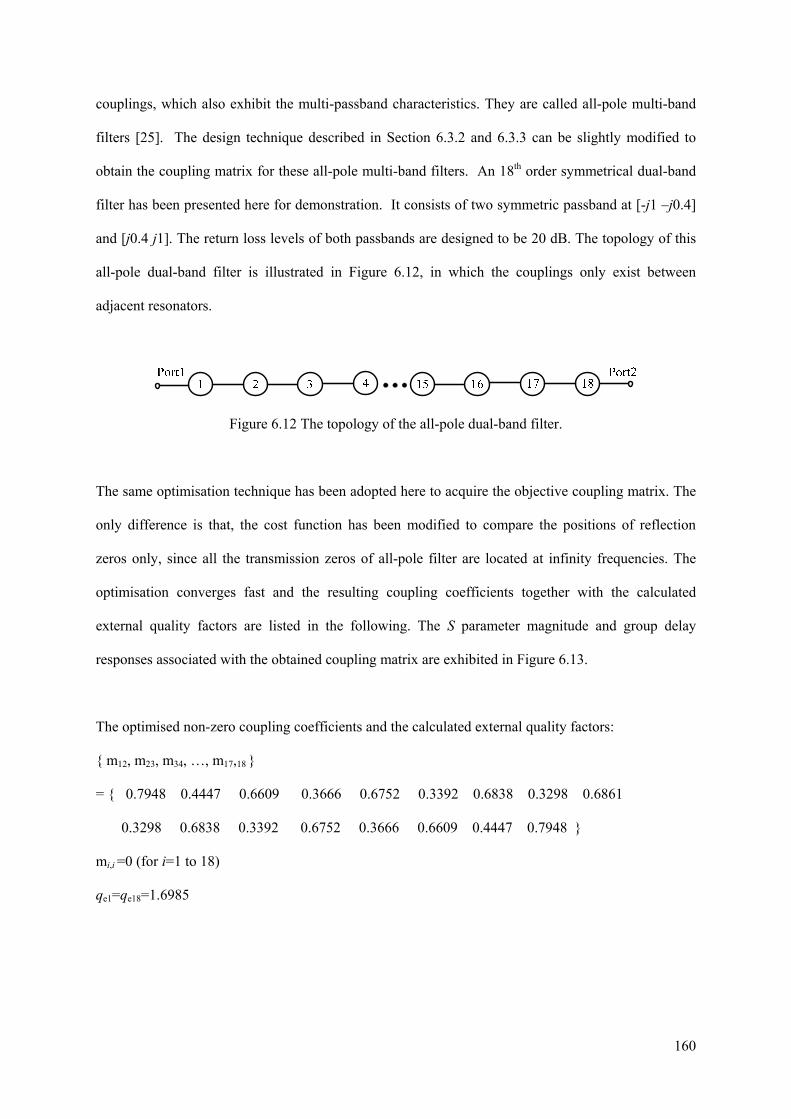
160
couplings, which also exhibit the multi-passband characteristics. They are called all-pole multi-band
filters [25]. The design technique described in Section 6.3.2 and 6.3.3 can be slightly modified to
obtain the coupling matrix for these all-pole multi-band filters. An 18th order symmetrical dual-band
filter has been presented here for demonstration. It consists of two symmetric passband at [-j1 –j0.4]
and [j0.4 j1]. The return loss levels of both passbands are designed to be 20 dB. The topology of this
all-pole dual-band filter is illustrated in Figure 6.12, in which the couplings only exist between
adjacent resonators.
Figure 6.12 The topology of the all-pole dual-band filter.
The same optimisation technique has been adopted here to acquire the objective coupling matrix. The
only difference is that, the cost function has been modified to compare the positions of reflection
zeros only, since all the transmission zeros of all-pole filter are located at infinity frequencies. The
optimisation converges fast and the resulting coupling coefficients together with the calculated
external quality factors are listed in the following. The S parameter magnitude and group delay
responses associated with the obtained coupling matrix are exhibited in Figure 6.13.
The optimised non-zero coupling coefficients and the calculated external quality factors:
m12, m23, m34, …, m17,18
= 0.7948 0.4447 0.6609 0.3666 0.6752 0.3392 0.6838 0.3298 0.6861
0.3298 0.6838 0.3392 0.6752 0.3666 0.6609 0.4447 0.7948
mi,i =0 (for i=1 to 18)
qe1=qe18=1.6985

161
(a)
(b)
Figure 6.13 Computed responses of the 18th order symmetrical all-pole dual-band filter. (a) S
parameter magnitude responses; (b) group delay response.
Figure 6.13 (a) shows the S parameter magnitude responses of this all-pole dual-band filter, which
looks similarly as a combination of two 9th order single band filters centred at -j0.7 and j0.7. The
primary advantage of all-pole dual-band filter is that it eliminates the need of power splitter/combiner
for these two single-band filters, which reduces the size and volume of the overall system. The
computed group delay response of this all-pole filter can be found in Figure 6.13 (b), in which large
-1.5 -1 0 1 1.50.4-0.4-70
-60
-50
-40
-30
-20
-10
0
Prototype Frequency, rad/s
S P
ara
met
er,
dB
S11S21
-2 -1 0 1 2-0.4 0.40
20
40
60
80
100
120
Prototype Frequency, rad/s
Gro
up D
ela
y, s

162
group delay variations especially at around the cut-off frequencies are attributed to the sharp
selectivity in the transmission magnitude responses.
Note that, the coupling coefficients presented in this example are all positive. Actually altering the
signs of these coupling coefficients does not affect the filter’s S parameter magnitude responses. This
is a common property shared by all filters with a single path topology, regardless of its passband
characteristics (i.e. single-band filter or multi-band filter). The flexibility of choosing signs of
coupling coefficients of all-pole multi-band filters may facilitate the physical implementations.
6.3.5.2 A general discussion of cross couplings
For the previous reported four examples, one may observe that the coupling coefficients of these
cross-coupled multi-band filters are of mixed signs, and may wonder the relationships between these
coupling coefficients and their corresponding magnitude responses. Briefly, the presence of finite
transmission zeros are attributed to the destructive interference between signals from different paths.
To generate finite transmission zeros, two essential requirements should be met, as (i) a phase shift
(i.e. 180 phase difference) between two paths; (ii) the same magnitude between these two paths,
which will ensure a zero magnitude after combining these two out-of-phase signals. The phase
difference between different paths are determined by the signs of coupling coefficients, and the signal
magnitudes of each path are controlled by the values of coupling coefficients.
Reference [39] has presented a simple rule to identify the positions of transmission zeros from the
signs of corresponding coupling coefficients. Cross-coupled coaxial cavity single passband filters
with various coupling topologies such as cascaded triplet and quadruplet have been discussed and
presented as verification examples. The same theory has been borrowed here to study multi-band
filters with multipath coupling diagrams. In order to simplify the problem, a sixth order symmetrical
dual-band filter, as shown in Figure 6.14, has been considered in this section as an example. It
consists of two passbands at [-j1 -j0.4] and [j0.4 j1]. The passband return loss levels are designed to
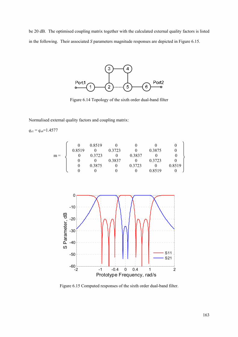
163
be 20 dB. The optimised coupling matrix together with the calculated external quality factors is listed
in the following. Their associated S parameters magnitude responses are depicted in Figure 6.15.
Figure 6.14 Topology of the sixth order dual-band filter
Normalised external quality factors and coupling matrix:
qe1 = qe6=1.4577
0 0.8519 0 0 0 0 0.8519 0 0.3723 0 0.3875 0 m = 0 0.3723 0 0.3837 0 0 0 0 0.3837 0 0.3723 0 0 0.3875 0 0.3723 0 0.8519 0 0 0 0 0.8519 0
Figure 6.15 Computed responses of the sixth order dual-band filter.
-2 -1 0 1 2-0.4 0.4-60
-50
-40
-30
-20
-10
0
Prototype Frequency, rad/s
S P
ara
met
er,
dB
S11S21

164
It can be observed that all the coupling coefficients of this dual-band filter are positive, the reason of
which will be explored in the following. Firstly, a lumped equivalent circuit model has been set up
for this dual-band prototype filter. In this model, the resonator is represented by a pair of shunt
capacitor and inductor, the positive coupling coefficients are modelled as a series capacitor and the
negative couplings are represented by a series inductor, as shown in Figure 6.16. Note that, for
physical implementation, the positive and negative coupling coefficient is relatively defined. This
means in Figure 6.16, the positive couplings can be represented by series inductors if negative
couplings are represented by series capacitors.
Figure 6.16 (a) A series capacitor, which is a dual of shunt inductor, represents positive coupling
coefficient in this example, the phase of S21: Φ21≈ +90. (b) A series inductor, which is a dual of
shunt capacitor, denotes negative coupling coefficient in this example, Φ21≈ -90. (c) Shunt capacitor
and inductor, which is employed to model the resonators of this filter in this example. Φ21≈ +90 (for
resonators below resonance, inductor dominants); Φ21≈ -90 (for resonators above resonance,
capacitor dominants); Φ21≈ 0 (for resonators at resonance).
For this example, transmitted signal will be split at resonator 2 and transferred from two different
paths (i.e. 2-3-4-5 and 2-5). Since resonators 1 and 6 have been shared by both paths, so these two
resonators have not been considered for phase calculation. Table 6.7 shows the total phase shift of
each path at four different frequency intervals, as listed in the following. It should be pointed out that
the passband used in this table corresponds to the entire passband of this prototype dual-band filter,
which ranges from -1 rad/s to 1 rad/s.

165
1. Passband-below resonance: this indicates the frequencies located inside the passband and
below the filter’s center frequency (i.e. -1 < Ω < 0 rad/s). For instance, the first transmission
zero in Figure 6.15 belongs to this interval. In this frequency interval, all the resonators are
resonating and thus do not contribute any phase shift.
2. Passband-above resonance: this represents the frequencies inside the passband and above the
filter’s center frequency (i.e. 0 < Ω < 1 rad/s). Similarly, resonators at this frequency interval
offer a zero phase shift.
3. Stopband-below resonance: this specifies the frequency points inside the left stopband (i.e. Ω
< -1 rad/s), at which each resonators provide a 90 phase shift.
4. Stopband-above resonance: similarly, this indicates the frequencies inside the right
stopband(i.e. Ω > 1 rad/s), at which each resonators give a -90 phase shift.
Compared with [39], two additional cases (i.e. the first and second case as listed above) have been
included and considered here due to the characteristics of dual-band filters (i.e. some transmission
zeros exist in the interval between [-1 1] rad/s).
Table 6.7 Phase difference between two paths
Passband
below resonance
Passband above
resonance
Stopband below
resonance
Stopband above
resonance Path 2-5 90 90 90 90
Path 2-3-4-5 90+90+90 90+90+90 90+90+90+90+90 90-90+90-90+90 Result Out phase Out phase In phase In phase
It is worth mentioning that the phase shift caused by the second and fifth resonator has been omitted
during the total phase calculation, because they are a common part of both paths. Besides, a few
conclusions with respect to this example can be drawn as
1. The sign of the coupling coefficient m12 and m56 can be freely altered without affecting the
filter’s response, since they are shared by all the paths and will not contribute any phase
difference.

166
2. Assigning negative signs to any two coupling coefficients among m23, m34 and m45, will
produce the exactly same filter responses as the one exhibited in Figure 6.15. Because that
alternation still result in an 180 phase difference between these two paths.
The discussion in this section is devoted to offering a very general method to understand the
relationships between coupling coefficients and their corresponding responses. Things will become
more complex in the case of asymmetrical filters, since the resonators will no longer resonate at the
same frequency. However, the transmission zeros are still produced as a result of destructive
interference between different transmit paths.
6.4 Practical Implementation of A Dual-Band Filter
The coupling matrix of an 8th order dual-band filter has been obtained using above optimisation
method and realized using waveguide technology to verify this design approach. This dual-band filter
is designed to operate at a centre frequency of 10 GHz with two symmetrically located passbands of
9.35 - 9.70 GHz and 10.30 - 10.65 GHz. The attenuation at the stopband is designed to be 45 dB and
achieved by introducing two transmission zeros at 9.88 GHz and 10.12 GHz. The return loss level of
both passbands is 20 dB. The topology of the filter is shown in Figure 6.17 (a). After getting the
characteristic polynomials of the lowpass prototype which fulfil the filter specifications, optimisation
was performed to generate the coupling matrix. The non-zero values of the coupling matrix after
optimisation and calculated external quality factor are: qe1 = qe8 =1.7278, m12=m78=0.6452,
m23=m67=0.0476, m34=m56=0.6623, m45=0.3786, m14=m58=-0.5389. The normalized coupling matrix
of the lowpass prototype is transformed to the practical frequency domain using the following
equation,
eieiq
QFBW
for i=1, N ; ij ijM FBW m for i =1 to N, j =1 to N (6.18)

167
where FBW is the fraction bandwidth of the dual-band filter. Giving Qe1=Qe8=13.2908,
M12=M78=0.0840, M23=M67=0.0062, M34=M56=0.0862, M45=0.0493, M14=M58=-0.0702. The physical
dimensions of this dual-band filter are acquired from these external quality factor and coupling
coefficients values by following an approach in [2]. These dimensions of the dual-band filter are
given in Figure 6.17 (b).
(a)
(b)
(c)
Figure 6.17 (a) Topology of the designed dual-band waveguide filter. (b) Configuration of the dual-
band filter with dimensions. This filter structure is symmetrical to the middle dotted line. b=10.16 mm.
L1 =46.5, L2 = L3 =20.72, L4 =23.6, L23 =9.53, ke=7.4, k12 =4.1, k23 =3.35, k34 =3.6, k45 =3, k14 =4.42, t1
=3, t2 =5. Unit: mm. (c) A photograph of one half of the dual-band filter with tuning screw holes,
b=10.16 mm. The first and eighth cavities operate at TE102 mode while the rest resonators operate at
conventional TE101 mode.
168
It should be noted that the cross couplings M14 and M58 have a negative sign as opposite to other
coupling coefficients. Normally in a rectangular waveguide these different signs are achieved by
using different coupling irises (i.e. capacitive or inductive irises). In this work, the coupling irises
used are exclusively capacitive, which makes the required negative coupling more difficult to realise.
As shown in Figure 6.17 (c), the negative couplings M14, M58 are achieved by employing two TE102
mode cavities 1 and 8, whereas the remaining six cavities operate with TE101 mode. A similar
principle has been used in [30] but in this case it is for all inductive coupling irises. The two desired
features for this kind of structure are: firstly, it is easy for CNC (Computer Numerical Control)
milling, since only two simple identical parts need to be fabricated and assembled. A good insertion
loss can be achieved using the E-plane split configuration. Secondly, this all-capacitive-iris split-block
structure is compatible with the multi-layer micromachining technology that has been developed for
fabricating millimetre-wave components, as discussed in Chapters 3 to 5. The design of this dual-band
filter has been scaled to WR-3 band and fabricated using this layered micromachining technology.
There are drawbacks of this all-capacitive coupling structure. It is not suitable for filters containing
small couplings. As the capacitive iris itself is a section of propagating waveguide, it causes a
relatively strong coupling even with small gaps [31]. Additionally, compared with an inductive-iris
filter, filters with capacitive irises have a higher rejection in the upper stopband, but a lower rejection
in the frequency range close to the cut-off of the feeding waveguide [32], as described in Chapter 4.
This results in the poorer-than-theory rejection at lower stopband. Moreover, standard X-band
waveguide resonator filters often suffer from poor higher stopband behaviour due to the appearance of
higher order modes and the resonances at higher harmonic frequencies, which occur at frequencies of
1.6 to 1.7 times the centre frequency. For the X-band filter presented in this work, situation becomes
worse since an extra resonance at 12.46 GHz introduced by the first and eighth cavity operating at the
unwanted TE103 mode was generated. This leads to the worse-than-theory attenuation performance at
the upper stopband.

169
The input/output of the filter is a WR-90 rectangular waveguide interface. The pieces were machined
from copper. The measured response before tuning was slightly shifted to higher frequencies. It was
identified that this shift was due to the round corners (with a radius of 1.6 mm) of each resonator,
which was not taken into account in the design. After adding tuning screws to the resonators and
coupling irises, the frequency shift was corrected and the measurement result showed excellent
agreement with the simulation as shown in Figure 6.18.
Figure 6.18 (c) shows the close-up view of measured and simulated passband responses, which have a
good agreement with each other. The simulated passband insertion loss, which is around 0.1 dB, is
mainly introduced by the finite unload quality factor (i.e. Qu) of the waveguide resonators. The effect
of this finite Qu on the filter’s transfer and reflection responses can be taken into account by adding a
real factor φ to the purely imaginary frequency variable s=jΩ to make it as s= φ+jΩ. φ is called
dissipation ratio and can be calculated from [3]
0 1
u u
f
BW Q FBW Q
(6.19)
where f0 is the filter centre frequency, BW is the designed bandwidth. As discussed previously in
Chapter 2, the unload quality factor Qu of a rectangular waveguide cavity with dimensions a, b and d
(i.e. length of resonator), operating in TE10l mode can be found as [36]
310
2 2 3 3 2 3 3
( ) 1
2 (2 2 )l
u
s
k ad bQ
R l a b bd l a d ad
(6.20)
where
2 210 ( ) ( )l
lk
a d
0
2sR
(6.21)

170
For this waveguide filter, six resonators are operating at TE101 mode and the other two are operating at
TE102 mode. By taking l=1 and 2 into equation (6.20), the Qu for the TE101 and TE102 mode can be
calculated as 7834 and 9196, respectively. The unloaded quality calculation does not factor in the
effect of the dielectric loss since nearly lossless air has been adopted as filling of the waveguide
cavities. Substituting an averaged unloaded quality factor 8175 and the fractional bandwidth 13.02%
into equation (6.19) yields a dissipation ratio φ of 9.4×10⁻⁴. Then the lowpass prototype filter’s S
parameter magnitude responses can be computed using the complex frequency variable s= φ+ jΩ.
Figure 6.19 shows the computed responses of three different unloaded quality factors, in which
Qu=2000 is considered for comparison purpose. It should be emphasized that, the practical bandpass
filter has the same insertion loss as its lowpass prototype at their corresponding frequency points. For
instance, the insertion loss of this X-band filter at the centre frequency of the first passband, is in
accordance with the insertion loss of the prototype filter at the normalized center frequency of its first
passband. It can be seen in Figure 6.19 (b) that the calculated average passband insertion loss of the
dual-band filter is around 0.1 dB, which is consistent with the CST simulation results. The above
presented method is applicable to predict the passband insertion loss of cross-coupled multi-band
filters implemented using other types of resonators.

171
(a)
(b)
(c)
Figure 6.18 The X-band dual-band filter performance obtained from CST simulation and
measurement after tuning. In the simulation, the conductivity of copper (σ = 5.813×10⁷ S/m) has been
used. (a) |S11| in dB. (b) |S21| in dB. (c) Detailed view of the S parameter responses at these two
passbands and the middle stopband.
8.5 9 9.5 10 10.5 11 11.5-50
-40
-30
-20
-10
0
Frequency, GHz
S11
, dB
SimulatedMeasured
8.5 9 9.5 10 10.5 11 11.5-80
-70
-60
-50
-40
-30
-20
-10
0
Frequency, GHz
S21
, dB
SimulatedMeasured
9.2 9.4 9.6 9.8 10.0 10.2 10.4 10.6 10.8-1.0
-0.8
-0.6
-0.4
-0.2
0.0
0.2
Simualted Measured
S P
ara
me
ter,
dB
Frequency, GHz
Passband S21Passband S21 Stopband S11
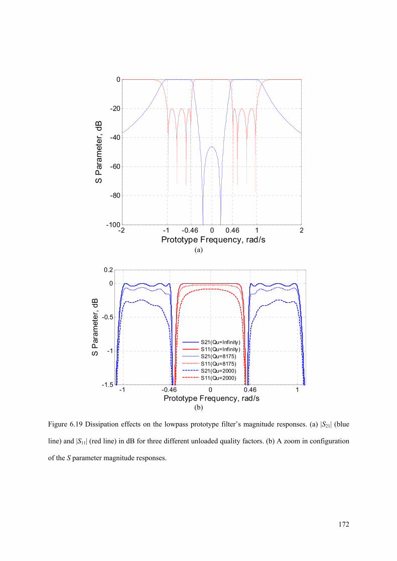
172
(a)
(b)
Figure 6.19 Dissipation effects on the lowpass prototype filter’s magnitude responses. (a) |S21| (blue
line) and |S11| (red line) in dB for three different unloaded quality factors. (b) A zoom in configuration
of the S parameter magnitude responses.
-2 -1 0 1 2-0.46 0.46-100
-80
-60
-40
-20
0
Prototype Frequency, rad/s
S P
ara
met
er,
dB
-1 0 1-0.46 0.46-1.5
-1
-0.5
0
0.2
Prototype Frequency, rad/s
S P
ara
met
er,
dB
S21(Qu=Infinity)S11(Qu=Infinity)S21(Qu=8175)S11(Qu=8175)S21(Qu=2000)S11(Qu=2000)
173
6.5 Conclusions
This chapter is devoted to describing a coupling matrix design approach based on a hybrid
optimisation algorithm which can be applied to cross-coupled multi-band filters having specified,
diverse topologies and responses. The characteristic polynomials fulfil the filter specifications are
generated by an iterative design technique based on polynomial fit. This iterative synthesis method
guaranteed convergence and is also able to generate polynomials for multi-band filter with different
return loss levels at each passband. After calculating the characteristic polynomials, a hybrid
optimisation technique is performed directly on the coupling matrix to seek the optimal set of
coupling coefficients. This hybrid optimisation technique employs a GA to choose strong initial
values for the following SQP search and was described in detail in [9]. At each optimisation iteration,
a novel and efficient cost function which measures the difference of the frequency locations of
reflection and transmission zeros is evaluated. This cost function eliminates the need of weighting
functions or searching. An equation to calculate external quality factors from polynomials has been
derived for filters with both symmetrical and asymmetrical responses and presented in this work. An
X-band dual-band waveguide filter has been designed, fabricated and measured to verify this design
approach; and excellent agreement between the simulation result and measured result has been
demonstrated. A novel technique to achieve both positive and negative couplings using the same kind
of coupling irises has been employed by the dual-band waveguide filter and presented.
References
[1] Roberto G. G. “Microwave Transversal Six-Band Bandpass Planar Filter for Multi-Standard
Wireless Applications”, IEEE RWS 2011
[2] Hong J.-S., Lancaster M.J.: ‘Microstrip filters for RF/ microwave applications’ (Wiley-
Interscience, 2001)

174
[3] Richard J. Cameron, Chandra M. Kudsia, Raafat R. Mansour: ‘Microwave Filter for
Communication Systems: Fundamentals, Design and Applications’ (Wiley, 2007)
[4] Atia W. A., Zaki. K. A, and Atia A. E.: ‘Synthesis of General Topology Multiple Coupled
Resonator Filters by Optimisation’, IEEE MTTS Int. Microw. Symp., Baltimore, USA, June 1998, pp.
821-824
[5] Amari S.: ‘Synthesis of Cross-Coupled Resonator Filters Using an Analytical Gradient-based
Optimisation Technique’, IEEE Trans. Microw. Theory Tech., 2000, 48, (9), pp. 1559–1564
[6] Mokhtaari M., Borenemann J., Rambabu K., Amari S.: ‘Coupling Matrix Design of Dual and
Triple Passband Filters’, IEEE Trans. Microw. Theory Tech., 2006, 54, (11), pp.3940-3946
[7] Amari S., Rosenberg U., and Bornemann J.: ‘Adaptive Synthesis and Design of Resonator Filters
With Souce/Load-Multiresonator Coupling’, IEEE Trans. Microw. Theory Tech., 2002, 50, (8),
pp.1969-1978
[8] Jayyousi A.B., Lancaster M. J.: ‘A Gradient-based Optimisation Technique Employing
Determinants for the Synthesis of Microwave Coupled Filters’, IEEE MTTS Int. Microw. Symp., Fort
Worth, USA, June 2004, pp. 1369-1372
[9] Nicholson G.L., Lancaster M. J.: ‘Coupling Matrix Synthesis of Cross-coupled Microwave Filters
using a Hybrid Optimisation Algorithm’, IET Microw. Antennas Propaga., 2009, 3, (6), pp. 950-958
[10] Bell H.C.: ‘Canonical Asymmetric Coupled-Resonator Filter’, IEEE Trans. Microw. Theory,
1982, 30, (9), pp.1335-1340
[11] Cameron R.J.: ‘General Coupling Matrix Synthesis Methods for Chebyshev Filtering Functions’,
IEEE Trans. Microw. Theory Tech., 1999, 47, (4), pp. 433–442
[12] Cameron R.J.: ‘Advanced Coupling Matrix Synthesis Techniques for Microwave Filters,’ IEEE
Trans. Microw. Theory, 2003, 51, (1), pp. 1-10
[13] Macchiarella G.: ‘Accurate Synthesis of In-Line Prototype Filters using Cascaded Triplet and
Quadruplet Sections’, IEEE Trans. Microw. Theory Tech., 2002, 50, (7), pp. 1779-1783
[14] Tamiazzo S., Macchiarella G.: ‘ An Analytical Technique for the Synthesis of Cascaded N-
Tuplets Cross-Coupled Resonator Microwave Filters Using Matrix Rotations’, IEEE Trans. Microw.
Theory Tech., 2005, 53, (5), pp. 1693-1698
[15] Lee J., Uhm M. S., Yorn I. B.: ‘A Dual-Passband Filter of Canonical Structure for Satellite
Application”, IEEE Microw. Wireless Compt. Letter, 2004
[16] Lenoir P., Bila S., Seyfert F., etc: ‘Synthesis and Design of Asymmetrical Dual-Band Bandpass
Filters Based on Equivalent Network Simplification’, IEEE Trans. Microw. Theory Tech., 2006, 54,
(7), pp. 3090-3097.
[17] Macchiarella G., Tamiazzo S.: ‘A Design Technique for Symmetric Dual-Band Filters’, IEEE
MTTS Int. Microw. Symp., 2005, pp. 115-118
[18] Macchiarella G., Tamiazzo S.: ‘Design Technique for Dual-Passband Filters’, IEEE Trans.
Microw. Theory Tech., 2005, 53, (11), pp.3265-3271

175
[19] Lee J., Sarabandi K.: ‘A Synthesis Method for Dual-Passband Microwave Filters’, IEEE Trans.
Microw. Theory Tech., 2007, 55, (6), pp.1163-1170
[20] Lee J., Sarabandi K.: ‘Design of Triple-Passband Microwave Filters Using Frequency
Transformations’, IEEE Trans. Microw. Theory Tech., 2008, 56, (1), pp.187-193
[21] Yu M., Tang W.C., Malarky A., Dokas V. Cameron R.J., and Wang Y.: “Predistortion technique
for cross-coupled filters and its application to satellite communication systems”, IEEE Trans.
Microwave Theory Tech., 2003, 51,(12), pp.2505-2515.
[22] Lamecki A., Kozakowski P., and Mrozowski M.: ‘Fast synthesis of coupled-resonator filters’,
IEEE Microw. Wireless Components Lett., 2004,14, (4), pp. 174-176
[23] Kozakowski P., Mrozowski M.: ‘Automated synthesis of coupled resonator filters with a given
topology’, 14th Int. Conf. Microw. Radar Wireless Communications, Gdansk, Poland, May 2002, pp.
373–376
[24] McGee W.: ‘Numerical Approximation Technique for Filter Characteristic Functions’, IEEE
Trans. Microw. Theory Tech., 1967, 14, (1), pp.92-94
[25] Deslandes Dominic, Boone Francois: ‘Iterative Design Techniques for All-Pole Dual-Bandpass
Filters’, IEEE Microw. Wireless Components Lett., 2007,17, (11), pp. 775-777
[26] Deslandes Dominic, Boone Francois: ‘An Iterative Design Procedure for the Synthesis of
Generalized Dual-Bandpass Filters’, International Journal of RF and Microw. Computer-aided
Engineering, 2009, 19, (5), pp.607-614
[27] Atia A. E., Williams A. E.: ‘Narrow-Bandpass waveguide filters’, IEEE Trans. Microw. Theory
Tech., 1972, 20, (4), pp. 258-265
[28] Matlab, the Math Works Inc., MA, USA
[29] Genetic Algorithm and Direct Search Toolbox User’s Guide, version 2, the MatchWorks
[30] Rosenberg U.: ‘New ‘Planar’ Waveguide cavity elliptic function filters’, Proc 25th Eur.
Microwave Conf., 1995, pp.524-527
[31] Ruiz-Cruz J. A., Zaki K. A., Montejo-GArai J. R. and Rebollar J. M.: ‘ Rectangular waveguide
elliptic filters with capacitive and inductive irises and integrated coaxial excitation’, IEEE MTTS Int.
Microw. Symp. Digest, June 2005, pp. 269-272
[32] Rosenberg U., Amari S., and Bornemann J.: ‘Inline TM110- Mode filters with high-design
flexibility by utilizing bypass couplings of nonresonating TE10/01 modes’, IEEE Trans. Microw.
Theory Tech., 2003, 51, (6), pp. 1735-1742
[33] F. Seyfert and S. Bila. General synthesis techniques for coupled resonator networks. IEEE
Microwave Magazine, 2007, (8) pp. 98-104.
[34] S. Amari, “On the maximum number of finite transmission zeros of coupled resonator filters with
a given topology,” IEEE Microwave Guided Wave Lett., 1999, vol. 9, no. 9, pp. 354–356.
[35] Herbert L. Thal, “Design of Microwave Filters with Arbitrary Responses,” International Journal
of Microwave and Millimeter-Wave Computer-Aided Engineering, 1997, vol.7, (3), pp. 208-221

176
[36] David Pozar: ‘ Microwave Engineering(3rd Edition)’ (John Wiley & Sons, Inc.)
[37] Optimisation Toolbox User’s Guide, version 6, the MatchWorks
[38] Pierre Jarry, Jacques Beneat: ‘Advanced Design Techniques and Realizations of Microwave and
RF Filters’ (John Wiley & Sons, Inc.)
[39] J. Brian Thomas, “Cross-Coupling in Coaxial Cavity Filters-A Tutorial Overview,” IEEE Trans.
Microw. Theory and Tech., 2003, 51, (4), pp.1368-1376

177
Chapter 7
Conclusions and Future Work
7.1 Conclusions
This thesis presented the work which can be broadly grouped into two separate categories: (i) SU-8
micromachined through waveguides and filters working at WR-10 band, WR-3 band and WR-1.5
band; (ii) design of coupling matrices for multiple passband filters using optimisation.
For the first part of the work, two thick SU-8 micromachining process procedures (i.e. single-layer
and two-layer processes), have been developed and applied successfully to the fabrication of terahertz
waveguide circuits. Additionally, two different measurement methods, namely, the integrated H-plane
back-to-back bends technique and the measurement metal block technique, have been utilised in this
work to achieve reliable and secure interconnection between the micromachined waveguide circuits
and the measurement network analysers. Nine terahertz waveguide components (i.e. through
waveguides, single-band filters and dual-band filters) have been designed, fabricated using the above
SU-8 micromachining techniques and measured using the two novel methods. These circuits are
measured to have excellent performance in terms of very low insertion losses. These results are
superior to the published work carried out by other research groups. This could be observed from the
comparisons shown in Figure 7.1 and Tables 7.1-7.2.
The SU-8 two-layer technique is based on two fully cross-linked SU-8 layers. In this work, this
technique has been employed to fabricate six WR-3 band waveguide circuits. The measurement
results of these circuits have been compared with the ones obtained from the previously developed
SU-8 single-layer technique. From the comparisons, it has been found that the two-layer technique
offers three major advantages over the single-layer process.
Firstly, this two-layer technique eliminates any possible air gaps between the layer 1 and 2, or 3 and 4
due to inter-layer cross-linking process. This produces better insertion loss performance for these
waveguide circuits, as shown in Figure 7.1, a comparison of the normalised insertion loss between six

178
different waveguide sections. Among them, the measured insertion loss of the SU-8 through
waveguide, obtained from two-layer process and mounted in the metal block, has reached a
comparable level with the commercially available CNC precision machined metal waveguide (i.e. the
calibration metal block fabricated by RAL). This SU-8 waveguide also shows better performance than
other WR-3 band micromachined waveguides published so far, as shown in Table 7.1.
Secondly, this two-layer technique produces a more robust device structures which lead to an
improved performance, especially for the filter device where the small iris structures make the
separate single-layer method less robust. As shown in Table 7.2, the filters obtained from two-layer
process show more than 1 dB improvement in the measured passband insertion loss.
Thirdly, this two-layer technique is particularly suitable for devices consisting of isolated
pieces/regions, such as the dual band filter circuit described in Chapters 4 and 5.
Therefore, it can be concluded that this SU-8 two-layer processing technique produces waveguide
circuits with improved performance as well as allows isolated regions/features within the circuits.
This enables the construction of more complex waveguide circuits in the future using this
micromachining technology.
In this thesis, two different measurement methods for SU-8 micromachined waveguide circuits are
provided in Chapters 4 and 5. Both of these two methods permit an accurate and reliable
interconnection with the standard flanges of the network analyzer. The main shortcoming associated
with the bend measurement method is the effect caused by the bend structures, whereas the main
drawback of the block measurement technique is that it cannot avoid the air gap at the interfaces
between the micromachined circuit and the metal block. The special bend structures and waveguide
choke flanges have been utilised by these two measurement techniques to address their associated
problems as mentioned above. According to the measurement performance of the SU-8 waveguides
and filters as reported in Chapters 4 and 5, it can be observed that both the bend structures and the
waveguide choke rings work well in terms of offering low insertion loss.

179
The comparisons in Tables 7.1 and 7.2 and in Figure 7.1 highlight that (i) the SU-8 through
waveguides and filters measured with the metal block have lower insertion losses; (ii) the SU-8
through waveguides with bends show sharply increased insertion losses at higher frequencies of the
WR-3 band, i.e. from around 300 GHz to 325 GHz.
The relatively higher insertion loss, exhibited by the SU-8 waveguide circuits with bends, can be
attributed to (i) the extra loss introduced by the bend structures at the two ends of the waveguide
circuits; (ii) the larger size of the SU-8 pieces for waveguide circuits with bends (i.e. 48 × 24 × 0.432
mm), which is more likely to result in localised air gap between SU-8 layers. The size of the SU-8
pieces of waveguide circuits mounted in the block is 14.97 × 10 × 0.432 mm. The former is around
seven times larger than the latter.
As shown in Figure 7.1, the SU-8 waveguides with bends are measured to have an insertion loss
which deteriorates at the frequencies above around 300 GHz. This transmission response shape is
shared by the SU-8 waveguides with bends obtained from both single-layer and two-layer fabrication
processes. This is caused by the presence of bend structures which are relatively more sensitive to
dimensional inaccuracy during the fabrication and misalignment during the assembling.
Briefly, both of these two measurement techniques have effect on the SU-8 micromachined circuit’s
performance. For the measurements using metal block, the loss of the metal waveguide sections can
be determined accurately through a calibration metal block and removed from SU-8 circuit’s
responses. The problems caused by the possible air gaps at the interfaces have also been addressed by
employing two waveguide choke flanges. However, for the measurements of bend devices, the effect
of the bend structures is more difficult to calculate accurately and remove. Therefore, for SU-8
waveguide circuits with bends, the presented measurement response is a result of both the SU-8
circuits and their integrated bends. This is the primary reason why the SU-8 circuits in the block have
better measured insertion losses than the ones with two bends.
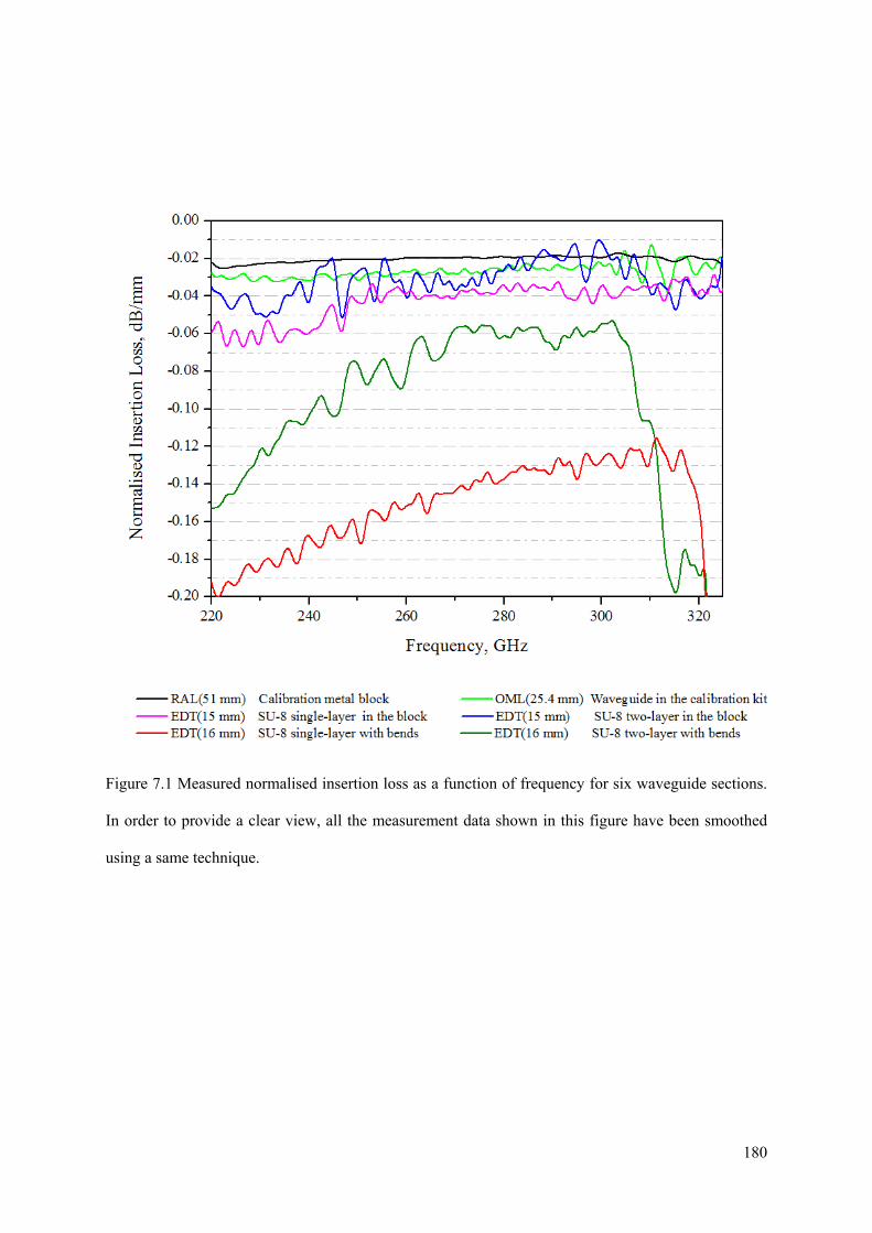
180
Figure 7.1 Measured normalised insertion loss as a function of frequency for six waveguide sections.
In order to provide a clear view, all the measurement data shown in this figure have been smoothed
using a same technique.
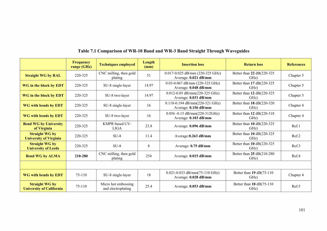
181
Table 7.1 Comparison of WR-10 Band and WR-3 Band Straight Through Waveguides
Frequency
range (GHz) Techniques employed
Length (mm)
Insertion loss Return loss References
Straight WG by RAL 220-325 CNC milling, then gold
plating 51
0.017-0.025 dB/mm (220-325 GHz) Average: 0.021 dB/mm
Better than 22 dB(220-325 GHz)
Chapter 5
WG in the block by EDT 220-325 SU-8 single-layer 14.97 0.03-0.067 dB/mm (220-325 GHz)
Average: 0.048 dB/mm Better than 17 dB(220-325
GHz) Chapter 5
WG in the block by EDT 220-325 SU-8 two-layer 14.97 0.012-0.05 dB/mm(220-325 GHz)
Average: 0.031 dB/mm Better than 12 dB(220-325
GHz) Chapter 5
WG with bends by EDT 220-325 SU-8 single-layer 16 0.118-0.194 dB/mm(220-321 GHz)
Average: 0.156 dB/mm Better than 18 dB(220-320
GHz) Chapter 4
WG with bends by EDT 220-325 SU-8 two-layer 16 0.056 -0.15 dB/mm(220-312GHz)
Average: 0.103 dB/mm Better than 12 dB(220-318
GHz) Chapter 4
Bend WG by University of Virginia
220-325 KMPR based UV-
LIGA 23.8 Average: 0.096 dB/mm
Better than 10 dB(220-325 GHz)
Ref.1
Straight WG by University of Virginia
220-325 SU-8 11.4 Average:0.263 dB/mm Better than 10 dB(220-325
GHz) Ref.2
Straight WG by University of Leeds
220-325 SU-8 8 Average: 0.75 dB/mm Better than 10 dB(220-325
GHz) Ref.3
Bend WG by ALMA 210-280 CNC milling, then gold
plating 254 Average: 0.015 dB/mm
Better than 25 dB(210-280 GHz)
Ref.4
WG with bends by EDT 75-110 SU-8 single-layer 18 0.021-0.033 dB/mm(75-110 GHz)
Average: 0.028 dB/mm Better than 19 dB(75-110
GHz) Chapter 4
Straight WG by University of California
75-110 Micro hot embossing
and electroplating 25.4 Average: 0.053 dB/mm
Better than 18 dB(75-110 GHz)
Ref.5

182
Table 7.2 Comparison of WR-10 Band and WR-3 Band Waveguide Filters
Frequency
range (GHz) Techniques employed
Filter Order
Measured fo and 3dB FBW
Passband Insertion loss Passband Return
loss References
Filter in the block by EDT
220-325 SU-8 single-layer 5 298.5 GHz,
9.7% 2 dB Better than 10 dB Chapter 5
Filter in the block by EDT
220-325 SU-8 two-layer 5 302.17GHz,
8.2% 1 dB Better than 12 dB Chapter 5
Filter with bends by EDT
220-325 SU-8 single-layer 4 293.2 GHz,
8.8% 3.3 dB Better than 16 dB Chapter 4
Filter with bends by EDT
220-325 SU-8 two-layer 4 295.02 GHz,
8.9% 1.5 dB Better than 10 dB Chapter 4
Filter by University of Virginia
220-325 KMPR based UV-
LIGA
Low-pass passband (220-275 GHz)
1.8 dB Better than 10 dB Ref.1
Filter with bends by EDT
75-110 SU-8 single-layer 4 88.47 GHz,
9.7% 1 dB Better than 15 dB Chapter 4
Filter by University of California
75-110 Micro hot embossing
and electroplating 5
96.77 GHz, 3.15%
1.22 dB Better than 9.3 dB Ref.6
Filter by Seoul National University
75-110 DRIE 4 93.7 GHz,
4.9% 1.3 dB Better than 16 dB Ref.7
Filter by Georgia Institute of Technology
75-110 DRIE 3 92.45 GHz,
4.83% 1.2 dB Better than 10 dB Ref.8

183
The second part of this thesis described a coupling matrix design procedure based on a hybrid
optimisation algorithm which can be applied to cross-coupled multi-band filters having specified,
diverse topologies and responses.
The characteristic polynomials fulfil the filter specifications are generated by an iterative design
technique based on polynomial fit. This iterative synthesis method guaranteed convergence and is also
able to generate polynomials for multi-band filter with different return loss levels at each passband.
After calculating the characteristic polynomials, a hybrid optimisation technique is performed directly
on the coupling matrix to seek the optimal set of coupling coefficients. At each optimisation iteration,
a novel and efficient cost function which measures the difference of the frequency locations of
reflection and transmission zeros is evaluated. This cost function eliminates the need of weighting
functions or searching; this yield faster and more reliable convergence of the optimisation. The
efficient cost function combined with the hybrid optimisation technique enables one to derive
coupling matrix for filters with complex responses and arbitrary topologies. Some optimisation
techniques do not converge for complex scenarios, and it has been demonstrated that the methods
presented in this thesis do by four examples. For instance Example-D descried in Chapter 6 is the first
ever demonstrated coupling matrix design for Quad-band filter with 16 resonators and 12 transmission
zeros.
Additionally, equation (6.17) has been derived to calculate external quality factors from polynomials
for filters with both symmetrical and asymmetrical responses.
An X-band dual-band waveguide filter has been designed, fabricated and measured to verify this
design approach; and excellent agreement between the simulation result and measured result has been
demonstrated. For this X-band dual-band filter, the negative cross couplings M14 and M58 are achieved
by altering the length of resonator 1 and 8 rather than using inductive coupling irises. This alternative
way to implement negative couplings is compatible with the layered micromachining technology
described in Chapter 3. The design of this X-band dual-band filter has been scaled to WR-3 band,

184
fabricated using the SU-8 micromachining techniques and measured using both the bends and metal
block measurement techniques, as described in Chapters 4 and 5.
7.2 Future Work
For the SU-8 micromachining work, further efforts can be made to (i) investigate waveguide circuit
structures which are less sensitive to the SU-8 layer thickness, such as inductive-iris-coupled filters;
(ii) look into possible mechanically tuning methods for these SU-8 micromachined waveguide circuits;
(iii) further improve the dimensional accuracy during fabrication process and the alignment accuracy
during assembling through process optimisation; (iv) further test the ability of this micromachining
technique by means of more complex circuits.
For the coupling matrix optimisation work discussed in the second part, it is suggested that the
following work should concentrate on studying methods for the calculation of multi-band filter’s
physical dimensions. Currently, after acquiring the initial dimensions through the design procedure
given in Chapter 2, a CST optimisation is performed to obtain the final dimensions of the multi-band
filter. However, for filters with large number of resonators and cross couplings, it is rather difficult to
acquire the desired physical dimensions within a reasonable time. For waveguide filters, mode
matching is a good potential solution to the above problem and it can be looked into in detail.
Additionally, the coupling matrix design approach presented in Chapter 6 can be extended to extract
coupling matrices for resonator coupled multiple-port circuits such as diplexers.
References
[1] Stanec J. R. and Barker N. S. “Fabrication and Integration of Micromachined Millimetre-Wave
Circuits” IEEE Microwave and Wireless component Letters, accepted for inclusion in the future issue
of this journal, according to IEEE explore

185
[2] Smith III C. H., Sklavounos A., and Barker N. S., “SU-8 Micromachining of Millimeter and
Submillimeter-wave Waveguide Circuits” Microwave Symposium Digest, 2009. IEEE MTT-S
International, 2009, pp. 961-964.
[3] Chow W. H., Champion A., and Steenson D. P.: ‘Measurements to 320 GHz of millimetre-wave
waveguide components made by high precision and economic micro-machining techniques,’ High
Frequency Postgraduate Student Colloquium, 2003, pp. 90-93.
[4] Kerr A.R., Litton C., Petencin G., Koller D., and Shannon M.: ‘Loss of Gold plated Waveguides at
210-280 GHz’ ALMA MEMO 585, 2009, pp. 1-6
[5] Sammoura F., Su Y.C., Cai Y., Chi C.Y.: ‘Plastic 95-GHz rectangular waveguides by Micro
Molding Technologies,’ Sens. Actuators A., Phys. 2006, 127, pp. 270-275.
[6] Sammoura F., Fuh Y.K., Lin L.: ‘Micromachined Plastic W-Band Bandpass Filters,’ Sens.
Actuators A., Phys. 2008, 147, pp. 47-51.
[7] Song S., Yoo C. S., Seo K. S.: ‘W-Band Bandpass Filter Using Micromachined Air-Cavity
Resonator with Current Probes,’ IEEE Microw. Wireless Components Lett. , 2010, 20, (4), pp. 205-
207.
[8] Li Y., Kirby P. L., Papapolymerou J.: ‘Silicon Micromachined W-Band Bandpass Filter Using
DRIE Technique,’ in Proc. 36th Eur. Microw. Conf., 2006, pp. 1271-1273
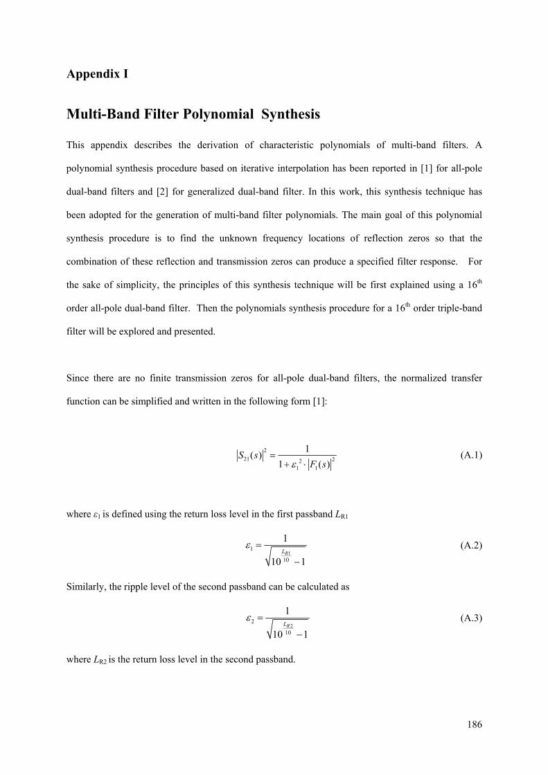
186
Appendix I
Multi-Band Filter Polynomial Synthesis
This appendix describes the derivation of characteristic polynomials of multi-band filters. A
polynomial synthesis procedure based on iterative interpolation has been reported in [1] for all-pole
dual-band filters and [2] for generalized dual-band filter. In this work, this synthesis technique has
been adopted for the generation of multi-band filter polynomials. The main goal of this polynomial
synthesis procedure is to find the unknown frequency locations of reflection zeros so that the
combination of these reflection and transmission zeros can produce a specified filter response. For
the sake of simplicity, the principles of this synthesis technique will be first explained using a 16th
order all-pole dual-band filter. Then the polynomials synthesis procedure for a 16th order triple-band
filter will be explored and presented.
Since there are no finite transmission zeros for all-pole dual-band filters, the normalized transfer
function can be simplified and written in the following form [1]:
2
21 221 1
1( )
1 ( )S s
F s
(A.1)
where ε1 is defined using the return loss level in the first passband LR1
11
10
1
10 1RL
(A.2)
Similarly, the ripple level of the second passband can be calculated as
22
10
1
10 1RL
(A.3)
where LR2 is the return loss level in the second passband.

187
It should be pointed out that F1(s) in this appendix has not been normalized to its highest-power
coefficient. This is different to the F(s) described in Chapter 6. The characteristic polynomial F1(s) of
an all-pole dual-band filter satisfies the following conditions [1]:
1. F1(s) is an Nth degree polynomial, which can be constructed using polynomial curve fitting by
interpolating through N+1 interpolated data points. N is the order of the filter.
2. F1(s) is oscillating in each passband. After normalizing the oscillation ripple level in the first
passband to 1, the ripple level of second passband can be expressed as ɛ2/ɛ1.
The synthesis of the polynomial F1(s) is achieved by use of the two properties above. Before
discussing the synthesis procedure in detail, an oversize problem of an all-pole dual-band filter will be
considered and two solutions to this over-defined problem will be explored. The characteristic
polynomial F1(s) of a 16th order all-pole asymmetrical dual-band filter is exhibited in Figure A.1,
which shows that F1(s) is oscillating between ±1 in the first passband [ -j1 -j0.25] and between ±ε2/ ε1
in the second passband [j0.358 j1].
The oscillating maxima and minima points of F1(s) are marked as green circles in Figure A.1. It
should be pointed out that four points at the passband band-edge frequencies (i.e. -j1, -j0.25, j0.358
and j1) are also identified as oscillating maxima/minima points of F1(s), although they are not actually
the extreme points. Figure A.2 illustrates the S parameter responses of this all-pole dual-band filter.
It can be observed from Figure A.1 and A.2 that, the locations of these maxima and minima points of
F1(s) coincide with the reflection maxima frequencies in the passbands. Additionally, the reflection
zeros of the S11 are occurring at the frequency locations where F1(s) equals to zero.

188
(a)
(b)
Figure A.1 Constructed polynomial F1(s) of the 16th order all-pole dual-band filter. The two
passbands are asymmetrically located at [-1 -0.25] rad/s and [0.358 1] rad/s. (a) F1(s) with critical
frequencies points; (b) detailed view of F1(s) at these two passbands.
-1 -0.5 0 1-0.25 0.358
0
5
10
15
20
25
30
35
40
45
Prototype Frequency, rad/s
F1(s
)
-1 -0.5 0 1-0.25 0.358-1.5
-1
-0.5
0
0.5
1
1.5
Prototype Frequency, rad/s
F1(s
)
ε2/ ε1
‐ε2/ ε1

189
Figure A.2 S parameter responses of the 16th order all-pole dual-band filter. The critical frequencies,
which are marked as green circles in this figure, are corresponding to the ones in Figure A.1
As shown in Figure A.1, the polynomial F1(s), with a degree of 16, could be built by polynomial
fitting these 18 extreme data points (as indicated by green circles). However, a perfect fitted 16th (i.e.
Nth) degree polynomial curve, which passes through all these 18 (i.e. N+2) points, cannot always be
obtained since only N+1 data points are needed for an exact fit of a Nth degree polynomial. To resolve
this oversized problem, one of the following interdependent parameters of a dual-band filter can be
relaxed [1].
1. The resonator number of each passband, which is not a good choice for solving the over-
defined problem since it only holds discrete values.
2. The bandwidth of each passband, which are determined by the band edge frequencies of each
passband. For the abovementioned all-pole dual-band filter, the 18th point can be abandoned
during the polynomial curve fitting. This will ensure the convergence and lead to the desired
ripple levels at each passband. However, the synthesised second passband bandwidth may be
different from specification since its upper band edge frequency (i.e. frequency of the 18th
point) has been set to be a flexible value.
-1.5 -1 -0.5 0 0.5 1 1.5
-60
-50
-40
-30
-20
-10
0
Prototype Frequency, rad/s
S P
ara
met
er,
dB
S11
S21

190
3. The return loss level of each passband, which are linked to the oscillating magnitude of each
passband via the ripple level. For instance, to synthesis the polynomial for the 16th order all-
pole filter, all the 18 points will be employed during the polynomial fitting. However, the
ripple level of the second passband will be relaxed, which implies that the second passband
will oscillate at an unknown value.
Both relaxing band edge frequencies and relaxing ripple levels methods have been discussed in [1].
In all the work presented in this thesis, the return loss level of one passband has been relaxed to offer
another degree of freedom, which will enable the convergence.
In the following, a detailed introduction will be given with regard to the generation of F1(s) from
these critical frequency points using an iterative technique. In the first passband, F1(s) is interpolated
through the nine maximum/minimum points. Their corresponding F1(s) values are altering between 1
and -1, as shown in Table-A1. The extreme points of the constructed polynomial F1(s) will be found
and their corresponding frequencies will be employed in the interpolation process for the following
iteration. As an illustration, the fitted data points at the third and fourth iteration have been computed
and presented. Figure A.3 shows the interpolated points at these two iterations. The new frequencies
(as indicates as ‘+’ in Figure A.3) of the first passband, at which maxima and minima of F1(s) occur,
are computed by differentiating the constructed polynomial curve F1(s) of Iteration 3 and equating it
to zero. These updated points, which are formed from calculated new frequencies and their
corresponding oscillation level (i.e. ±1), are used in Iteration 4 for the polynomial construction. The
initial frequencies of these interpolated points, as shown in Table-A.1, are computed by assuming
equal distribution in the passbands.

191
Table-A1 Interpolated points of F1(s) at some iterations
Iteration 1 Iteration 3 Iteration 4 Iteration 9
frequency F1(s) frequency F1(s) frequency F1(s) frequency F1(s)
First P
assban
d
-1.000 1 -1.0000 1 -1.0000 1 -1.0000 1
-0.9063 -1 -0.9858 -1 -0.9824 -1 -0.9817 -1
-0.8125 1 -0.9236 1 -0.9307 1 -0.9278 1
-0.7188 -1 -0.8139 -1 -0.8429 -1 -0.8407 -1
-0.6250 1 -0.6915 1 -0.7218 1 -0.7252 1
-0.5313 -1 -0.5603 -1 -0.5827 -1 -0.5883 -1
-0.4375 1 -0.4255 1 -0.4377 1 -0.4419 1
-0.3438 -1 -0.3051 -1 -0.3090 -1 -0.3105 -1
-0.2500 1 -0.2500 1 -0.2500 1 -0.2500 1
Secon
d P
assban
d
0.3981 0 0.3702 0 0.3697 0 0.3699 0
0.4784 0 0.4572 0 0.4488 0 0.4514 0
0.5586 0 0.5636 0 0.5688 0 0.5707 0
0.6389 0 0.6876 0 0.6913 0 0.6951 0
0.7191 0 0.7869 0 0.8056 0 0.8078 0
0.7994 0 0.8854 0 0.8945 0 0.8991 0
0.8796 0 0.9492 0 0.9576 0 0.9630 0
0.9599 0 0.9788 0 0.9907 0 0.9959 0

192
(a)
(b)
Figure A.3 Fitted polynomial curve F1(s) at the third iteration with the interpolated points. (a) A
general view. (b) Detailed view of these two passbands. Green/red circles indicate the interpolated
points of the first/second passband at the current iteration (i.e. Iteration 3); Blue plus signs represent
the frequencies for the next iteration (i.e. Iteration 4). For the first passband, two points at (-1, 1) and
(-0.25, 1) will be fixed during every iteration, since their frequencies are the first passband band-edge
frequencies.
-1 -0.5 0 0.5 1-5
0
10
20
30
40
50
Prototype Frequency, rad/s
F1(s
)
-1 -0.5 0 0.5 1-1.5
-1
-0.5
0
0.5
1
1.5
Prototype Frequency, rad/s
F1(s
)
193
In the second passband, where the ripple level is relaxed, the eight reflection zeros (i.e. where F1(s)
equals to zero) rather than the extreme value points, have been employed in the interpolation, since
the oscillating magnitude of the second passband is unknown. Table-A.1 has listed the eight zeros
points at Iteration 3, which are also shown in Figure A.3. The position of the reflection zeros in the
second passband, for the next iteration, can be calculated by linearizing the problem as [1]
8
, 11 , 1
( )jj j k k
k k k
F sy y s
s
for j=1 to 9 (A.4)
where yj represents the oscillating magnitude for the next iteration, which holds the same absolute
value for these nine extreme points. yj indicates the extreme values at the current iteration, sj are the
corresponding frequency locations of these yj, sk,k+1denote the frequency locations of reflection zeros
in the second passband. Equation (A.4) is a system of equations, which is formed with nine equations
and nine variables (i.e. ∆sk,k+1 (for k=1 to 8) and yj ).
The position of the zeros in the second passband, for the next iteration, sk,k+1 , can be obtained by
solving the system of equations (A.4), since they are linked via the following equation:
, 1 , 1 , 1k k k k k ks s s for k=1 to 8 (A.5)
The interpolated points of the second passband at the 4th iteration are computed using equations (A.4)
and (A.5), and are shown in Figure A.3 and Table-A.1. The polynomial F1(s) for the next iteration is
created by interpolating through these seventeen new data points. A cost function, which measures
the frequency location differences of the interpolated points between the current iteration and the
following iteration, has been calculated to evaluate the fitness of the constructed polynomial F1(s), as
given by

194
1
11
( ) ( )N
j j ji
cost s i s i
(A.6)
where sj(i) indicates the frequency location of the ith interpolated points at the jth iteration. The
convergence of this iterative technique is fast and only a few iterations are needed for acquiring the
desired polynomial F1(s), as shown in Figure A.4. The final cost (i.e. cost at Iteration 9) is 3.2e-11 and
the final seventeen interpolated data points are exhibited in Table-A.1. At Iteration 9 the calculated yj
(i.e. ε2/ε1 ) from equation (A.4) is 0.3148, from which the return loss level of the second passband LR2
can be computed as 30 dB.
Figure A.4 Cost of each iteration
The same iterative synthesis technique can be applied to obtain the polynomials for other all-pole
multi-band filters with more than two passbands. In that case, only the ripple level or bandwidth of
one passband needs to be relaxed to provide a degree of freedom to ensure the convergence.
Additionally, the same polynomial synthesis principles can be invoked to produce polynomials for
multi-band filters with finite transmission zeros (TZs). For filters with finite TZs, the transfer
function is given by [2]
1 2 3 4 5 6 7 8 90
0.1
0.2
0.3
0.4
0.5
0.6
Iteration
Co
st

195
2
21 2
2 11
1( )
( )1
( )
S sF sP s
(A.7)
where P(s) is the characteristic polynomial which can be expressed with a unit multiplying form as
TZ
TZP1( ) ( )
N
iP s s s
(A.8)
where NTZ is the number of finite transmission zeros and sTZP denotes the frequency locations of these
transmission zeros. The same interpolating principles as described above for all-pole dual-band filters,
can be employed to synthesis the polynomials of multi-band fitlers with finite transmission zeros here,
since polynomial F1(s)/P(s) is still oscillating in each passband. Therefore, a fitted polynomial curve
F1(s), which is passing through the extreme points [Ωi, ±1·P(Ωi)] in the first passband and points[Ωj,
±ɛk/ɛ1·P(Ωj)] in the kth passband can be constructed. Besides, the frequencies at which the extreme
values of F1(s)/P(s) appear can be calculated by differentiating F1(s)/P(s), which may be expressed as
1 1'( ) ( ) ( ) '( ) 0F s P s F s P s (A.9)
where the prime signs indicates the derivative of the polynomial.
Next the polynomials of a 16th order symmetrical triple-band filter will be presented as an example.
Figure A.5 shows the S parameter responses of this triple-band filter after polynomial synthesis. It has
been shown that the three passbands are symmetrical located at [-j1 -j0.6], [-j0.3 j0.3] and [j0.6 j1].
The return loss levels of the first and third passband LR1 is designed to be 20 dB and the return loss
levels of the second passband is designed to be 30 dB. Eight transmission zeros are positioned at
±j1.15, ±j0.5, ±j0.45, ±j0.405.

196
The final constructed polynomial F1(s), together with a graph of F1(s)/P(s) is illustrated in Figure A.6,
which shows that F1(s) is not oscillating with the same magnitude, whereas F1(s)/P(s) is oscillating
between an equal amplitude value in each passband. This property of F1(s)/P(s) has been used to
produce polynomial F1(s) by means of polynomial fitting technique, as described earlier.
The synthesis convergence is also fast, as exhibited in Figure A.7. After 14 iterations the cost
decreases to 4.5e-12.
Figure A.5 S parameter response of the 16th triple-band filter
-2 -1.5 -1 -0.5 0 0.5 1 1.5 2-70
-60
-50
-40
-30
-20
-10
0
Prototype Frequency, rad/s
S P
ara
met
er,
dB
S11S21
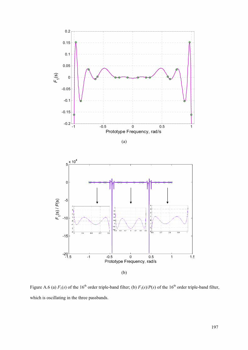
197
(a)
(b)
Figure A.6 (a) F1(s) of the 16th order triple-band filter; (b) F1(s)/P(s) of the 16th order triple-band filter,
which is oscillating in the three passbands.
-1 -0.5 0 0.5 1-0.2
-0.15
-0.1
-0.05
0
0.05
0.1
0.15
0.2
Prototype Frequency, rad/s
F1(s
)

198
Figure A.7 Cost of the 16th triple-band filter polynomial synthesis at each iteration.
It is worth mentioning that the above triple-band filter example has been specially chosen for
demonstration purpose. Actually, there will still be an oversized problem if all the parameters of the
multi-band filter are fixed. The positions of transmission zeros, which have a direct effect on the
rejection level of stopbands, is an extra adjustable factor for the filters with finite TZs. In this thesis,
the positions of TZs have been relaxed and adjusted to offer another degree of freedom, which ensures
the convergence of the polynomial synthesis procedure. It works following an approach as illustrated
in Figure A.8. The approach consists of a two layer synthesis procedure, in which the outer layer loop
specifies the positions of TZs and the inner layer loop uses the relax ripple iterative technique to
extract the objective polynomial F1(s) for the supplied set of TZs. By applying this synthesis
procedure, the passband bandwidths and return loss levels are preserved; however, the target rejection
levels of stopbands cannot always be achieved. One of the passband return loss levels or one of the
passband bandwidths can be relaxed to ensure the synthesis convergence in the case where the
stopband rejection is the most critical specification. This means that the last step of the flowchart in
1 2 3 4 5 6 7 8 9 10 11 120
0.1
0.2
0.3
0.4
0.5
0.6
0.7
Iteration
cost

199
Figure A.8 (i.e. “Compare LR with specification”) can be modified to “Compare attenuation with
specification” , when strict stopband specification is required. In some cases this modification will
result in a slightly out of specification return loss levels of one passband.
Figure A.8 Flowchart of the polynomial synthesis procedure for multi-band filters with finite TZs.
This synthesis procedure will guarantee the passband specifications (i.e. bandwidths, return loss
levels), however, the specification on stopband attenuation may not be satisfied.
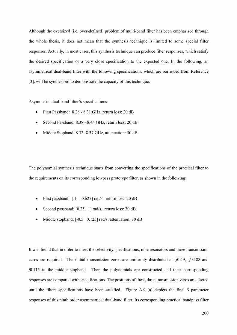
200
Although the oversized (i.e. over-defined) problem of multi-band filter has been emphasised through
the whole thesis, it does not mean that the synthesis technique is limited to some special filter
responses. Actually, in most cases, this synthesis technique can produce filter responses, which satisfy
the desired specification or a very close specification to the expected one. In the following, an
asymmetrical dual-band filter with the following specifications, which are borrowed from Reference
[3], will be synthesised to demonstrate the capacity of this technique.
Asymmetric dual-band filter’s specifications:
First Passband: 8.28 - 8.31 GHz, return loss: 20 dB
Second Passband: 8.38 - 8.44 GHz, return loss: 20 dB
Middle Stopband: 8.32- 8.37 GHz, attenuation: 30 dB
The polynomial synthesis technique starts from converting the specifications of the practical filter to
the requirements on its corresponding lowpass prototype filter, as shown in the following:
First passband: [-1 -0.625] rad/s, return loss: 20 dB
Second passband: [0.25 1] rad/s, return loss: 20 dB
Middle stopband: [-0.5 0.125] rad/s, attenuation: 30 dB
It was found that in order to meet the selectivity specifications, nine resonators and three transmission
zeros are required. The initial transmission zeros are uniformly distributed at -j0.49, -j0.188 and
j0.115 in the middle stopband. Then the polynomials are constructed and their corresponding
responses are compared with specifications. The positions of these three transmission zeros are altered
until the filters specifications have been satisfied. Figure A.9 (a) depicts the final S parameter
responses of this ninth order asymmetrical dual-band filter. Its corresponding practical bandpass filter

201
responses are shown in Figure A.9 (b). The return loss level of the second passband has been relaxed
and computed as 19.8 dB, which is extremely close to the expected 20 dB. The specification on the
middle stopband attenuation has also been satisfied, as shown in Figure A.9.
(a)
(b)
Figure A.9 (a) Final S parameter magnitude responses of the 9th order asymmetrical dual-band
prototype filter. The three transmission zeros are located at -j0.48, -j0.19 and j0.1. (b) S parameter
magnitude responses of the practical dual-band filter.
-1.5 -1 1 1.5-0.625 0.25-70
-60
-50
-40
-30
-20
-10
0
Prototype Frequency, rad/s
S P
ara
met
er,
dB
S11S21
8.28 8.448.31 8.38-70
-60
-50
-40
-30
-20
-10
0
Frequency, GHz
S P
ara
met
er,
dB
S11S21

202
References
[1] Deslandes Dominic, Boone Francois: ‘Iterative Design Techniques for All-Pole Dual-Bandpass
Filters’, IEEE Microw. Wireless Components Lett., 2007,17, (11), pp. 775-777
[2] Deslandes Dominic, Boone Francois: ‘An Iterative Design Procedure for the Synthesis of
Generalized Dual-Bandpass Filters’, International Journal of RF and Microw. Computer-aided
Engineering, 2009, 19, (5), pp.607-614
[3] Lunot V., Bila S., Seyfert F.: ‘Optimal Synthesis for Multi-Band Microwave Filters’, IEEE MTT-
S International, June 2007, pp. 115-118.

203
Appendix II
Publications
1. X. Shang, M. Ke, Y. Wang , M.J. Lancaster, “Micromachined W-band Waveguide and Filter with Two Embedded H-Plane Bends,” IET Microwave, Antenna & Propagation, 5, (3), pp. 334-339, 2011
2. X. Shang, M. Ke, Y. Wang , M. J. Lancaster, “A Micromachined WR-3 Waveguide Filter With Embedded Bends,” IET Electronics Letter, 47, (9), 2011
3. X. Shang, M.J. Lancaster, M. Ke, Y. Wang, “Measurements of Micromachined Sub-millimetre Waveguide Circuits,” 76th ARFTG conference, Clearwater, Florida, USA, December 2010
4. M. Ke, X. Shang, Y. Wang, M. J. Lancaster, “Improved Insertion Loss for a WR-3 Waveguide Using Fully Cross-Linked Two-layer SU8 Processing Technology,” the 12th
International Symposium on RF-MEMS and RF-Microsystems (MEMSWAVE 2011), Athens, Greece, June 27-29, 2011.
5. M. Ke, X. Shang, Y. Wang, M. J. Lancaster, “High Performance WR-3 Waveguide Devices using SU8 Photoresist Micromachining Technology,” Submitted to IEEE Transactions on MTT
6. X. Shang, Y. Wang, G.L. Nicholson, M.J. Lancaster, “ The Design of Multiple-Passband
Filters using Coupling Matrix Optimisation,” IET Microwave, Antenna & Propagation, Accepted subject to minor corrections
7. X. Shang, Y. Wang, M. J. Lancaster, “Coupling Matrix Optimisation of Triple-Passband Filters,” IET Proceeding of the 2nd Annual Seminar of Passive RF & Microwave Components, Glasgow, U.K., 30th March 2011
Note: Papers (1)-(3) are available at IEEE Xplore Digital Library;
Papers (4)-(7) are attached.

204
Improved Insertion Loss for a WR-3 Waveguide Using Fully Cross-Linked Two-layer SU8
Processing Technology
Maolong Ke, Xiaobang Shang, Yi Wang, Michael J. Lancaster
School of Electrical, Electronic and Computing Engineering, University of Birmingham, Birmingham, B15 2TT, UK, Tel: 0121 4147965
Abstract - Fully cross-linked two-layer SU8
photoresist technology has been successfully developed and used to fabricate a WR-3 waveguide with two back-to-back right-angle bends at both ends. The right angle bends are designed to facilitate accurate connection with external waveguides for measurement purpose. The insertion loss has shown significant improvement over previous results obtained using separate SU8 layers. It is believed that elimination of localized air gaps between the fully cross-linked interface of two adjacent SU8 layers contributed to the improvement. The two-layer SU8 processing technology can be extended into multi-layer technology, which will greatly expand the scope of device applications. The technology is particularly useful in devices which consist of isolated regions or weakly joint parts, which is very difficult to fabricate using previously reported separate layer processing technique.
I. Introduction
There is a growing interest in fabricating high performance components at millimetre wave and submillimetre wave frequencies using micromachining technologies. Among many reported so far [1], thick layer SU8 photoresist technology has displayed some important advantages in terms of near vertical sidewalls, very high aspect ratio (>30:1) as well as only relatively cheap and standard photolithographic equipment is needed, hence easily accessible to many. In contrast, other competing technologies, such as Si deep reactive ion etching (DRIE) [2] requires expensive etching machine, while LIGA process [3] requires synchrotron radiation source. In fact, SU8 has been successfully employed by us to make many high frequency components, including WR-3(220-325 GHz) waveguide, filter and slot antenna [4-6].
However, all the SU8 devices made so far are based on separate layers bonded/assembled together. Typically, for example, a waveguide device was split into 4 equally thick layers and all the layers were made in one mask processing. The
layers were then released from Si substrate, metal coated and then bonded/assembled together. The drawback of this method is that it is quite difficult to completely avoid localized air gaps between the different layers because the SU8 surfaces are not perfectly flat. When two uneven surfaces come into contact, air gaps will form among the lower surface regions. As is well known, air gaps have deleterious effect on device performance, resulting in current leakage and higher loss.
In this paper, we report results of a 300 GHz waveguide device with two back to back right angle bends obtained through a new fabrication method. The paper is organized as follows: in the next section (II), device details are reported, which is followed by a detailed description of the fabrication method (III). Measurements and discussions will be given in Section IV, which is followed by conclusions in Section V.
II. Device details
In order to facilitate measurement of a 300 GHz rectangular waveguide device, two H-plane back to back right angle bends were designed as shown in Fig. 1. This allows for reliable and accurate

205
(a)
(b)
(c)
Fig. 1: (a) WR-3 waveguide structure with two right angle bends (unit mm), (b) top view of the first/fourth layer, (c) top view of the second/third layer.
interconnection with standard waveguide flanges. Fig. 1(b) and (c) shows the top view of layer 1/4 and 2/3. The waveguide is only about 16 mm long by 0.432 mm wide. Each layer is, however, 48 mm long by 24 mm wide in order to fully accommodate all the alignment pin holes as wells as holes for flange screws (more details later).
III. Fabrications
Previously this device was fabricated using one mask photolithographic process, in which all four layers were printed onto one mask and processed together in one lithographic step. Each layer is then individually silver coated and bonded/assembled as described in [4]. The disadvantage of such a method is that localized air gaps may form after bonding due to the surface unevenness. These air gaps are likely to lead to increased insertion losses due to current leakage. In order to eliminate the air gaps, we have here developed two-layer SU8 processing technology. Instead of making four separate layers, two layers were processed together to form one half of the waveguide. The final device was formed by combining the two halves together. The fabrication details will be published elsewhere, here is a brief outline of how it was achieved. Two masks were used instead of one. In mask 1 only the layer 1 and 4 were printed with alignment marks, in mask 2 the layer 2 and 3 printed along with the same alignment marks. Firstly, a 432 µm thick layer of SU8 was spun onto a Si substrate, pre-baked, UV exposed with mask 1 and post-baked.
Then another 432 µm thick SU8 layer was added onto the top of the layer, pre-baked, UV exposed with mask 2 after careful alignment and post-baked again. During the second UV exposure, both the top and bottom layers were exposed together, hence the second post exposure bake will crosslink the two layers together to form one fully joint piece, hence eliminate the air gaps between the interface. Fig. 2 displays a photo of the processed SU8 device using this new technique where two layers were fully crosslinked together to form a half of the designed waveguide. Finally the waveguide was formed by aligning and bonding the two halves together after silver coating.
Fig. 2: A photo of the processed SU8 piece
where two layers were fully cross-linked together to form a half of the said waveguide
This method eliminates any air gaps between
layer 1/2 and 3/4 interfaces, but it can still leave some air gaps between the middle interface (layer 2/3). However, since the waveguide was designed to split in the E-plane and little current is expected to cross the middle interface, hence any air gaps there is not expected to have large adverse effect on the device performance.
IV. Measurements and discussions
During the measurement, the micromachined waveguide was sandwiched between two brass plates, as shown in Fig. 3. Standard waveguide flanges were inserted into the opening region on the clamping brass to connect directly with the micromachined waveguide circuits [4]. Screws on the flanges go straight through the micromachined waveguide and into nuts at the opposite plate. The alignment pins provide the accuracy to which the two halves are aligned as well as the accuracy to which the device is aligned to the external flange. The screws are used to clamp the layers together as well as fixing the external flange to the micromachined waveguide. The length of waveguide excluding the bends is 15.95 mm, which is made sufficiently long to allow adequate separation between the flanges of measurement equipment to avoid blocking of pins and screws from the other side. The measurements were carried out on an Agilent E8361A Network Analyzer with a WR-3 extension T/R module at test port 1 and a receive-only T module at test port
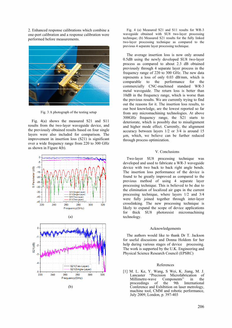
206
2. Enhanced response calibrations which combine a one-port calibration and a response calibration were performed before measurements.
Fig. 3 A photograph of the testing setup
Fig. 4(a) shows the measured S21 and S11 results from the two-layer waveguide device, and the previously obtained results based on four single layers were also included for comparison. The improvement in insertion loss (S21) is significant over a wide frequency range from 220 to 300 GHz as shown in Figure 4(b).
(a)
(b)
Fig. 4 (a) Measured S21 and S11 results for WR-3 waveguide obtained with SU8 two-layer processing technique; (b) Measured S21 results for the fully linked two-layer processing technique as compared to the previous 4 separate layer processing technique.
The average insertion loss is now only around
0.5dB using the newly developed SU8 two-layer process as compared to about 2.3 dB obtained previously through 4 separate layer process in the frequency range of 220 to 300 GHz. The new data represents a loss of only 0.03 dB/mm, which is comparable to the performance for the commercially CNC-machined standard WR-3 metal waveguide. The return loss is better than 10dB in the frequency range, which is worse than the previous results. We are currently trying to find out the reasons for it. The insertion loss results, to our best knowledge, are the lowest reported so far from any micromachining technologies. At above 300GHz frequency range, the S21 starts to deteriorate, which is possibly due to misalignment and higher mode effect. Currently, the alignment accuracy between layers 1/2 or 3/4 is around 15 µm, which, we believe can be further reduced through process optimization.
V. Conclusions
Two-layer SU8 processing technique was developed and used to fabricate a WR-3 waveguide device with two back to back right angle bends. The insertion loss performance of the device is found to be greatly improved as compared to the previous method of using 4 separate layer processing technique. This is believed to be due to the elimination of localized air gaps in the current processing technique, where layers 1/2 and 3/4 were fully joined together through inter-layer crosslinking. The new processing technique is likely to expand the scope of device applications for thick SU8 photoresist micromachining technology.
Acknowledgements
The authors would like to thank Dr T. Jackson for useful discusions and Donna Holdom for her help during various stages of device processing. The work is supported by the U.K. Engineering and Physical Science Research Council (EPSRC)
References
[1] M. L. Ke, Y. Wang, S Wei, K. Jiang, M. J. Lancaster “Precision Microfabrication of Millimetre-wave Components” in the proceedings of the 9th International Conference and Exhibition on laser metrology, machine tool, CMM and robotic performance, July 2009, London, p. 397-403
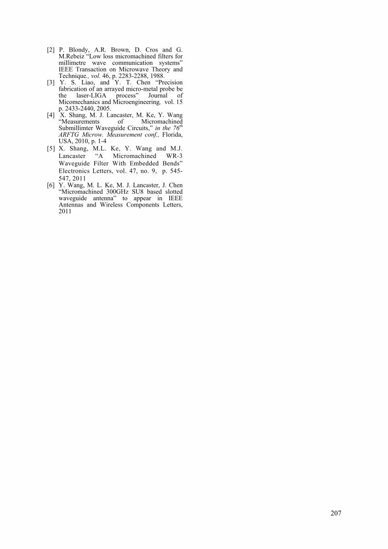
207
[2] P. Blondy, A.R. Brown, D. Cros and G. M.Rebeiz “Low loss micromachined filters for millimetre wave communication systems” IEEE Transaction on Microwave Theory and Technique., vol. 46, p. 2283-2288, 1988.
[3] Y. S. Liao, and Y. T. Chen “Precision fabrication of an arrayed micro-metal probe be the laser-LIGA process” Journal of Micomechanics and Microengineering, vol. 15 p. 2433-2440, 2005.
[4] X. Shang, M. J. Lancaster, M. Ke, Y. Wang “Measurements of Micromachined Submillimter Waveguide Circuits,” in the 76th ARFTG Microw. Measurement conf., Florida, USA, 2010, p. 1-4
[5] X. Shang, M.L. Ke, Y. Wang and M.J. Lancaster “A Micromachined WR-3 Waveguide Filter With Embedded Bends” Electronics Letters, vol. 47, no. 9, p. 545-547, 2011
[6] Y. Wang, M. L. Ke, M. J. Lancaster, J. Chen “Micromachined 300GHz SU8 based slotted waveguide antenna” to appear in IEEE Antennas and Wireless Components Letters, 2011
208
High Performance WR-3 Waveguide Devices using SU8 Photoresist Micromachining
Technology
Maolong Ke, Xiaobang Shang, Yi Wang, Member, IEEE and Mike J. Lancaster, Senior Member, IEEE
Abstract— This paper demonstrates a two-layer SU8
photoresist micromachining technology that has similar performance to conventionally machined metal. The technology is demonstrated in the WR-3 band, but has applicability up to and beyond 1 THz. Three different WR-3 band circuits, namely a WR-3 band waveguide, a bandpass filter and a dual-band filter are demonstrated. For the measurements, a conventionally precision machined metal block was used for the WR-3 band waveguide and the bandpass filter to achieve accurate interconnection with standard waveguide flanges. Whereas for the dual-band filter, two back-to-back right-angle bends were added in order to achieve reliable waveguide interconnection without using the metal block. A measured average insertion loss of 0.03 dB/mm has been achieved for the 14.97 mm long straight through waveguide. This is comparable to the loss of around 0.02 dB/mm for a standard metal waveguide at this frequency. The 5th order waveguide filter exhibits an 8% 3 dB bandwidth at a central frequency of around 300 GHz. The minimum passband insertion loss was measured to be around 1 dB and return loss was better than 10 dB throughout the passband. The results showed a notable improvement over those obtained from the separate SU8 layer technique which was also used to make the same devices for comparison. To further demonstrate the advantages of the new two-layer SU8 micromachining technique, the dual band filter included isolated regions in the waveguide channels which would have not been possible for micromachining using the previous separate single layer technique. The performance of the micromachined dual band filter was excellent in terms of very low insertion losses on both bands.
Index Terms—SU-8 micromachining, WR-3, waveguide, filter, millimeter wave devices, terahertz filters
I. INTRODUCTION HERE is a growing interest in millimeter-wave (mm-wave) and terahertz components in the frequency range from 100
GHz to 10 THz for their various potential applications in security scanning, atmospheric monitoring, medical imaging and ultrafast wireless communications [1-2]. Traditionally, metal milling is used to make passive components such as waveguides and filters. However, as the operating frequency continues to increase, and device dimensions continue to decrease, traditional metal milling methods are becoming increasingly time-consuming and expensive for making such components [3]. Photolithographic based micromachining technology has therefore attracted growing attention. Many different micromachining technologies have been reported in literature, among them three have been found most suitable for thick layer or three dimensional (3D) fabrication: namely Si
deep reactive ion etching (DRIE) [4-5]; LIGA based thick layer electroplating [6-7] and SU8 photoresist [8-12]. Previously we have compared these three technologies and found thick layer SU8 photoresist technology affords the best dimensional accuracy and at the same time with the least capital investment required [13], therefore making it a highly desirable choice for high precision and high performance applications. However, as the operating frequency rises to 300 GHz and above, device performance of micromachined circuits has not been comparable to the precision CNC machined circuits. For example, insertion loss for a precision CNC machined waveguide at 300GHz frequency is around 0.02 dB/mm, whereas best reported insertion losses so far from micromachined waveguides is typically an order of magnitude higher (> 0.2 dB/mm) as shown in Table 1. Performance improvement is therefore of high priority if the micromachined circuits are to compete with the traditional CNC precision machined circuits. As reported previously, we started our microfabrication investigation with a separate single-layer SU8 processing technique, and produced very good performance for a W-band waveguide and a waveguide filter [14], however as frequency moved up to around 300GHz, the device performance was less impressive [15-16]. The average sidewall roughness of our micromachined SU8 circuits has been measured with AFM to be very low [17], in the order of a few tens of nm, hence the roughness of the waveguide walls should not be a major factor for the reduced performance. The previous waveguides were formed by joining layers of metal coated SU8, and it is therefore believed that the joins may have an adverse effect on performance. We have therefore developed a fully joined two-layer SU8 processing technique which would be expected to produce better performing devices by removing critical joints. Previously, this type of joined SU8 multi-layers technique has found some applications in microfluidics [18-19], its use for millimetre wave circuits has been reported [11] but for different context circuits at 1.6THz, with no discussion of the attenuation.
In the separate single-layer micromachining process, a WR-3 waveguide device was split into 4 equally thick separate layers. SU8 is spun onto a silicon wafer and all the layers were made by photolithography using a single, one mask processing step. The layers were then released from Si substrate, metal coated and then bonded/assembled together. The drawback of this method is that it is difficult to avoid localized air gaps between the different layers because the
T

209
SU8 surfaces are not perfectly flat. Typically, surface roughness and thickness non-uniformity are in the order of several micrometers. When two uneven surfaces come into contact, air gaps can form along the joining surface regions. Air gaps have deleterious effect on device performance, resulting in current leakage and higher loss.
In this paper, a new multilayer SU8 processing technology is developed for 300 GHz components. The previous separate layers processing technique was also used to make the same devices for comparison. We then proceeded to design a dual band filter using the new fully joined SU8 two-layer processing technique, which is not possible for previous technique. The paper is organized as follows: The device design and structure details are presented in Section II, which is followed by a detailed description of fabrication procedure in Section III. Measurements and discussions will be presented in Section IV and finally conclusions in Section V.
II. DEVICE DESIGN AND STRUCTURE DETAILS
Both the WR-3 straight through waveguide and the 5th order bandpass filter consist of nominally 4 equally thick layers of
Fig. 1: A cross sectional view from either end of the waveguide and the bandpass filter devices which consists nominally four layers, each layer has a thickness of 432 µm. a=864 µm, b= 432 µm.
432 µm each. Fig. 1 illustrates their cross sectional view. Both devices were split in E-plane to minimise possible losses. For the bandpass filter, a 5th order Chebyshev type with a ripple bandwidth of 9% centered at 300 GHz has been designed following the approach in [20]. To meet the filter specification the external Q and the coupling coefficients between resonators are calculated to be: Qext=10.793, k12=k45=0.078, k23=k34=0.057 [17]. In order to be consistent with the micromachining process of this layered structure, all capacitive coupling irises have been adopted here to provide the required external Q and coupling coefficients. Full-wave modelling was carried out in CST [21], and Fig. 2 illustrates some critical dimensions achieved after optimization.
Fig. 2 A schematic side-view diagram of the fifth order iris coupled WR-3 filter. Drawing is not to scale. Some critical dimensions of the filter: h1=178
µm, h2= 300 µm, h3=341 µm, L1=696 µm, L2=645 µm, L3=640 µm, t1=100 µm, t2=143 µm, b=432 µm
Fig. 3 A schematic side-view diagram of the eighth order WR-3 band dual-band waveguide filter. This filter structure is symmetric to the middle dotted line. Some critical dimensions of the filter: L1=1580 µm, L2=L3=712 µm, L4=808 µm, L23=175 µm, t1=100 µm, t2=150 µm, g12=187 µm, g23=93 µm, g34=149 µm, g45=150 µm, g14=210 µm, ge=326 µm, b=432 µm
A WR-3 band eighth order dual-band waveguide filter, with a center frequency of 280 GHz and a fractional bandwidth of 13%, has also been designed and fabricated using the joined two-layer SU8 micromachining processing technology. The initial dimensions of this WR-3 filter are scaled from the design of an X-band (i.e. WR-90) dual-band waveguide filter, as reported in [22]. A full-wave optimisation was performed and the final dimensions are shown in Fig. 3. Two H-plane bends, as presented in [16], have been employed here for accurate and secure connection with measurement ports. Note that, there are two isolated parts in the second and third SU8 layer, as highlighted in Fig.3. If the circuit were made of four separate layers, then these isolated layers would not be connected and therefore could not be accurately positioned in the final circuit. This prevents the usage of single SU8 layer fabrication technique for this circuit.
III. FABRICATION DETAILS
Initially the through waveguide and the bandpass filter were fabricated using all four layers, each device was fabricated using one mask and processed in a standard photolithographic procedure. The four separate layers were then released from Si substrate, silver coated and finally bonded together by applying adhesive through device edges. As mentioned above, the disadvantage of such a method is that localized air gaps can exist after bonding because the surfaces of the SU8 layers were not perfectly flat. When two uneven surfaces were brought into contact, localized air gaps would form. These air gaps are likely to lead to increased insertion losses due to current leakage. In order to eliminate the air gaps, we have developed two-layer SU8 processing technology. Instead of making four separate layers and then bonding them together, two layers were processed in succession to form a fully joined one half of the waveguide or the filter. The full processing details are as follows. A 4” Si wafer of around 1000 µm in thickness was used as a substrate and 5.2 grams of SU8 50 photoresist were spun onto the substrate. Prebake was carried out on a precisely levelled hotplate and temperature was stepped from 650C for about 20 minutes to 950C for four and half hours. The main purpose of the initial baking step at 650C was to assist self planarization of the SU8 photoresist and improve the uniformity of the final processed layers. This

210
happens because the SU8 photoresist became less viscous at the elevated temperature and its mobility enhanced, therefore self planarization process proceeded on the precision levelled hotplate. The second baking step at 95oC was to dry out the solvent. The wafer was then exposed under a mercury lamp UV source from a Canon PLA-510 mask aligner. The mercury lamp emits three main beams at 365, 405 and 436 nm in addition to a broad but weak background level. Initially an L39 optical filter was used to filter out signals under 400 nm and the wafer was exposed 5 times 40 seconds in order to expose through the thick SU8 layer. It is well known that long wavelength signal lines such as the 405 nm line can penetrate much deeper into SU8 layer than 365 nm signal line, but it is less effective in generating a strong acid for cross linking purpose [10]. A PL360 optical filter was then used to filter out signals under 360 nm, so the main i-line 365nm signal was used to expose the SU8 photoresist for 3 times 40 seconds. Alignment marks are transferred from the first mask onto the first SU8 layer during this exposure stage, which will then be used to align with the second mask later. The wafer was then softly baked at 70oC for 15 minutes to allow for weak crosslinking to take place and at the same time avoid too much stress between the crosslinked SU8 and Si substrate. Another 5.2 grams of fresh SU8 was then added onto the sample and the fresh solvent was dried out at 70oC for about 9 hours. Once again this lower temperature baking was designed to reduce the stress between the SU8 and Si substrate. The sample was then carefully aligned under the mask aligner with the help of alignment marks, so that the second layer lain precisely on top of the first. The exposure details are the same as before for the first layer. After the second exposure, the wafer was post-exposure baked at 65oC for 5 minutes followed by 95oC for 30 minutes to allow for strong crosslinking across all the exposed areas. During the second exposure stage, the long wavelength signal lines from the mercury lamp will be able to penetrate all the way through both SU8 layers to reach Si substrate, hence both layers will be crosslinked and joined together during the second post-exposure baking stage. Finally the wafer was developed in EC solvent for 45 minutes with an in-house designed agitation jig and released from Si substrate through sodium hydroxide solution. Fig. 3 displays the schematic diagram of some key steps for the aforementioned SU8 two-layer processing procedure.
Fig. 3 A schematic diagram of some key steps for SU8 two-layer processing
The final product is a fully joined two SU8 layers forming one half of the waveguide/filter device. After cleaning thoroughly with running de-ionized water for 2 minutes followed by ultrasonic bath for 15 minutes, the pieces were then blown dry and loaded into a vacuum chamber for metallization. A Cressington 308 metal coater was used for metallization, which started with oxygen plasma cleaning for 45 seconds, followed by a thin Cr sputtering layer of around 5 nm for improved adhesion, and finally a 2 µm thick silver layer was thermally evaporated onto the device to form the main conducting layer. The sample holder rotated continuously at a tilted angle in order to coat the important sidewalls. Fig. 4 shows photos of one half of the silver coated waveguide (a) and filter (b).
a b
Fig. 4 (a) Photo of one half of a silver coated waveguide and (b) one half of a silver coated filter.
IV. MEASUREMENTS AND DISCUSSIONS
A conventionally machined metal block comprised of two separate pieces has been employed to mount the micromachined WR-3 band waveguide and the 5th order bandpass filter, as illustrated in Fig. 5. The metal block is split along the E-plane of a WR-3 waveguide so is in two separated pieces. Four screws and four location pins across both pieces are used to provide an accurate and secure fit between them. The micromachined waveguide and filter are placed in the middle of the block and standard WR-3 waveguide flanges (i.e. UG-387) are connected to the block ends. Two choke rings, with optimized dimensions, as given in Fig. 5, have been adopted at the interfaces between the metal block and micromachined circuits, to reduce the effect of possible interconnection gaps [14].

211
Fig. 5: Photograph of the measurement metal block which was split along the E-plane of a WR-3 waveguide. Four screws are employed to achieve intimate contact between Piece I and Piece II. A PTFE screw is used here to push the micromachined circuits towards Piece II. Dimensions of the choke ring are: R1=0.523 mm, R2=0.673 mm and the depth of the choke ring is 0.26 mm.
Measurements were performed using an Agilent E8361A
Network Analyzer with OML WR-3 extension modules subject to enhanced response calibration. A metal calibration block with a length of 51 mm was measured and had an average insertion loss of 1 dB, corresponding to an attenuation of 0.02 dB/mm. For the measurement results of the micromachined waveguide and filter, the loss of the 36 mm long metal waveguide of the measurement block has been taken into consideration and removed. Fig. 6a displays the measured S-parameter performance for the through waveguide device obtained through the fully joined two-layer processing procedure discussed here. Similar results obtained through separate layer processing technique are also shown for comparison. Both devices exhibited very low insertion loss. As shown clearly in Fig. 6(b), with an expanded scale for S21, both techniques produced a waveguide circuit with an insertion loss of around 0.5 dB, with the two-layer technique marginally superior. This insertion loss represented a loss of 0.03 dB/mm, which is comparable to the results of between 0.013 to 0.025 dB/mm obtained from gold plated CNC precision machined metal waveguides as given in Table 1. This represents, to our best knowledge, the best reported insertion loss in this frequency range from any micromachined technique. The return loss (S11) is better than 15dB in majority of the band.
a
b
Fig. 6 The measured S21 and S11 performance (a) for the WR-3 waveguide with the expanded view of S21 shown in (b).
Fig. 7 displays the S parameter performance for two WR-3
waveguide filters obtained again from the two different
a
b
Fig. 7 the measured S21 and S11 performance for the 5th order waveguide filter obtained from the two different techniques, simulation results are also shown for comparison. (b) is an expanded view of S21.
fabrication techniques. The simulation data is also shown for comparison. Both measured results exhibited a narrower-than-expected 3 dB bandwidth which is believed to be due to the inaccuracies among the gaps of the coupling irises. The simulation results predicted a 3 dB bandwidth of around 10.6%, while experimentally the results were 9.7% for separate layer technique and about 8.2% for the joined two-layer one. The iris gaps was measured to be narrower than designed by around 5% on average, this accounts for part of the observed narrowing (less than 0.5%) according to our
220 240 260 280 300 320
-30
-20
-10
0
S11
(Two-Layer)
S21
(Two-Layer)
S11
(Single-Layer)
S21
(Single-Layer)
Frequency (GHz)
S P
aram
eter
(dB
)
220 240 260 280 300 320-1.5
-1.0
-0.5
0.0
0.5
S 21(d
B)
Frequency(GHz)
S21
(Two-Layer)
S21
(Single-Layer)
220 240 260 280 300 320-60
-50
-40
-30
-20
-10
0
S11
(Single-Layer)
S21
(Single-Layer)
S11
(Two-Layer)
S21
(Two-Layer)
S11
(Simulated)
S21
(Simulated)
S Pa
ram
eter
(dB
)
Frequency(GHz)
280 300 320-6
-5
-4
-3
-2
-1
0
S21
(Single-Layer)
S21
(Two-Layer)
S P
aram
eter
(dB
)
Frequency(GHz)

212
simulation. The rest is likely due to the inaccuracies in other critical dimensions, from the lengths of resonators to the width of the waveguide. The insertion loss improved from an average of around 2 dB for the separate layer technique to about 1 dB with the joined two-layer one. The return loss also showed an improvement for the joined two-layer device over the separate layer one and was better than 10 dB throughout the passband. It is believed the improvements in both cases resulted from the fact that the jointed layer technique produced more robust coupling irises, where little movement is expected from them during the final bonding and assembly stage, whereas in the separate layer case, the irises can move sideways when pressing them together.
For the dual band filter measurement, the micromachined circuits were sandwiched between two brass plates as shown in figure 8. Standard waveguide flanges were inserted into the opening region on the clamping brass to connect directly with the micromachined circuits [14]. Screws on the flanges go straight through the micromachined circuits onto nuts at the opposite plate. The alignment pins provide the accuracy to which the two halves are aligned, as well as the accuracy to which the device is aligned to the external flange. The screws are used to clamp the layers together as well as fixing the external flange to the micromachined circuits. The length of circuits excluding the bends is 15.95 mm, which is made sufficiently long to allow adequate separation between the flanges of measurement equipment to avoid overlapping of pins and screws from the other side. The measurements were again carried out on the Agilent E8361A Network Analyzer with a WR-3 extension T/R module at test port 1 and a receive-only T module at test port 2. Enhanced response calibrations, which combine a one-port calibration and a response calibration were performed before measurements.
Fig. 8 A photograph of the testing setup
The measured performance is displayed in Fig. 9. It can be observed from Fig. 9 that, the filter responses have been shifted to the left hand side by around 5 GHz, whereas the measured average passband insertion loss is around 0.8 dB. The frequency shift is likely to be due to the thickness inaccuracy or variation across the device, especially the second layer thickness. At this stage we are unable to measure the second layer thickness accurately as it is way above our Daktak operating range (45µm). However, our simulation
shows a 20 µm thicker than the designed 432 µm layer would explain the observed 5GHz frequency shift.
Fig.9 Measurement and simulation results of the WR-3 band dual-band waveguide filer.
V. CONCLUSIONS
A fabrication technique based on two fully crosslinked SU8 layers is developed and used for the first time to fabricate a WR-3 straight waveguide and filter. The results are compared with the previously developed separate SU8 layer technique and found the technique produced a more robust device structures which lead to an improved performance, especially for the filter device where the small iris structures make the separate layer method less robust. This technique eliminates any possible air gaps between the layer 1 and 2, or 3 and 4 due to inter-layer crosslinking process. The measured insertion losses of around 0.03 dB/mm for through waveguides and around 1.0 dB for the filters are, to the best of the authors’ knowledge, the best performance ever demonstrated for any WR-3 micromachined straight through waveguide and resonator bandpass filter. The waveguide insertion loss has finally reached a comparable level with the commercially available CNC precision machined metal waveguide (~0.02
220 240 260 280 300 320-70
-60
-50
-40
-30
-20
-10
0
S 21(d
B)
Frequency(GHz)
S21
(Simulated)
S21
(Measured)
220 240 260 280 300 320
-40
-30
-20
-10
0S 11
(dB
)
Frequency(GHz)
S11
(Simulated)
S11
(Measured)

213
dB/mm). This new technique is particularly suitable for devices consisting of isolated pieces/regions, such as the dual band filter circuit. The high performance achieved for this dual band filter circuit demonstrated the key advantage of the new two-layer process over the previous separate layer one. The new processing technique offers added flexibility for device designers in their pursuit of ever increased performance by allowing isolated features within the circuits.
Techniques described here will in future allow very complex passive waveguide circuits to be constructed. Because of the photolithographic process there is no cost penalty for increasing complexity. Now that the low loss performance of the waveguide circuits has been proven, and with integration of active circuits, micromachined antennas and the inherent self packaging of the SU8 process, this technology is of considerable interest for terahertz circuits of the future.
REFERENCES [1] I. Hosako, N. Sekine, M. Patrashin and et al, “At the Dawn of a New
Era in Terahertz Technology,” Proceedings of the IEEE, vol. 95, No. 8, pp.1611 – 1623, 2007
[2] J. R. Stanec, C. H. Smith, and N. S. Barker “Integrating Micromachined circuits into Submillimeter Systems” European Microwave Conference (EuMc), 2010, pp. 53-56
[3] A. R. Kerr, C. Litton, G. Petencin, D. Koller, and M. Shannon “ Loss of Gold plated Waveguides at 210-280 GHz” ALMA MEMO 585, 2009, pp. 1-6
[4] P. Blondy, A. R. Brown, D. Cros, and G. M. Rebeiz “Low loss micromachined filters for millimetre wave communication systems” IEEE Transaction on Microwave Theory and Technique., vol. 46, pp. 2283-2288, 1998.
[5] Y. Li, P. Kirby, and J. Papapolymerou, “Silicon micromachined W band folded and straight waveguides using DRIE technique,” Microwave Symposium Digest, 2006. IEEE MTT-S International, June 2006, pp.
1915–1918, [6] Y. S. Liao and Y. T. Chen, ” Precision fabrication of an arrayed micro-
metal probe be the laser-LIGA process”, Journal of Micomechanics and Microengineering, vol. 15, pp. 2433-2440, 2005
[7] R. Arnaudov, B. Avdjiiski, A. Kostov, et al, “Novel micro-contacts in microwave chip carriers Developer by UV-LIGA process”, IEEE Transaction on Advanced Packaging, vol. 29, pp. 122-130, 2006
[8] H. Lorenz, M. Despont, N. Fahrni, N. Labianca, P. Vettiger, and P. Renaud, “EPON SU-8: A low-cost negative resist for MEMS,” in Proceedings of Micro Mechanics Europe, Barcelona, 1996, pp. 32-35.
[9] C. H. Smith III, A. Sklavounos, and N. S. Barker, “SU-8 Micromachining of Millimeter and Submillimeter-wave Waveguide Circuits” Microwave Symposium Digest, 2009. IEEE MTT-S International, 2009, pp. 961-964.
[10] J. D. Williams and W. Wang, “Study on the postbaking process and the effects on UV lithography of high aspect ratio SU-8 microstructures” Journal of Microlithography, Microfabrication, and Microsystems, vol. 3, pp. 563-568, 2004
[11] C. H. Smith III, Haiyong Xu, and N. S. Barker “Development of a multi- layer SU-8 process for terahertz frequency waveguide blocks” Microwave Symposium Digest, 2005. IEEE MTT-S International, 2005, pp. 439-442
[12] W. H. Chow, A. Champion, and D. P. Steenson, “Measurements to 320 GHz of millimetre-wave waveguide components made by high precision and economic micro-machining techniques” High Frequency Postgraduate Student Colloquium, 2003, pp. 90-93.
[13] M. L. Ke, Y. Wang, S Wei, K. Jiang, and M. J. Lancaster “Precision Microfabrication of Millimetre-wave Components” in the proceedings of the 9th International Conference and Exhibition on laser metrology, machine tool, CMM and robotic performance, July 2009, London, pp. 397-403
[14] X. Shang, M. Ke, Y. Wang, and M, J. Lancaster, “Micromachined W-Band Waveguide and Filter with Two Embedded H-plane Bends,” IET
Microw. Antennas Propagat., vol. 5, pp. 334-339, 2011 [15] X. Shang, M. J. Lancaster, M. Ke, and Y. Wang, “Measurements of
Micromachined Submillimter Waveguide Circuits,” in 76th ARFTG Microw. Measurement conf., Florida, USA, 2010
[16] X. Shang, M.L. Ke, Y. Wang, and M.J. Lancaster “A Micromachined WR-3 Waveguide Filter With Embedded Bends” Electronics Letters, vol. 47, no. 9, pp. 545-547, 2011
[17] Y. Wang, M. L. Ke, M. J. Lancaster, and J. Chen “Micromachined 300 GHz SU8 Based Slotted Waveguide Antenna” IEEE Antennas and wireless propagation letters, vol. 10, pp. 573-576, 2011
[18] J. Carlier, S. Arscott, V. Thomy, J. C. Fourrier, F. Caron, J. C. Camart, C. Druon, and P. Tabourier “Integrated microfluidics based on multi-layered SU-8 for mass spectrometry analysis” Journal of Micromechanics and Microengineering, Vol. 14, pp. 619-624, 2004
[19] A. Mata, A. J. Fleischman, and S. Roy “Fabrication of multi-layer SU-8 microstructures” Journal of Micromechanics and Microengineering, vol. 16, pp. 276-284, 2006
[20] U. Rosenberg, S. Amari, and J. Bornemann, “ Inline TM110 Mode Filters with High-design Flexibility By Utilizing Bypass Couplings of Nonrenonating TE10/01 modes,” IEEE Trans. Microw. Theory Tech., vol. 51, pp.1735-1742, 2003
[21] CST Microwave Studio Germany, CST GmbH, 2006. [22] X. Shang, Y. Wang, G. L. Nicholson, and M. J. Lancaster, “ The Design
of Multiole-Passband Filters using Coupling Matrix Optimisation”, submitted to IET Microw. Antennas Propagat.
[23] J. R. Stanec and N. S. Barker “Fabrication and Integration of Micromachined Millimeter-Wave Circuits” IEEE Microwave and Wireless component Letters, accepted for inclusion in the future issue of this journal, according to IEEE explore

214
Frequency Range
(GHz) Techniques Employed
Length (mm)
Insertion Loss Return Loss References
(Years)
Straight WG by RAL
220-325 CNC Milling,
then gold plating 51
0.017-0.025 dB/mm(220-325 GHz)
Average: 0.021 dB/mm
Better than 22 dB(220-325 GHz)
Our calibration
Straight WG by EDT
220-325 Single SU-8 layer 14.97 0.03-0.067 dB/mm (220-325
GHz) Average: 0.048 dB/mm
Better than 17 dB(220-325 GHz)
Presented here
Straight WG by EDT
220-325 Multiple SU-8
layer 14.97
0.012-0.05 dB/mm(220-325 GHz)
Average: 0.031 dB/mm
Better than 12 dB(220-325 GHz)
Presented here
Straight WG by University
of Virginia 220-325
KMPR based UV-LIGA
6.04 0.203-0.47 dB/mm(220-325
GHz) Average: 0.336 dB/mm
Average: 17.49 dB Ref.[23] (2010)
Straight WG by University
of Virginia 220-325 SU-8 11.4
0.088-0.438dB/mm(220-325GHz)
Average:0.263 dB/mm Average: 15 dB
Ref. [9] (2009)
A Gold Plated
Waveguide by ALMA
210-280 CNC Milling,
then gold plating 254
0.013-0.017dB/mm(210-280GHz)
Average: 0.015 dB/mm Better than 25 dB
Ref. [3] (2009)
Straight WG by University
of Leeds 220-325 SU-8 8
Average: 0.75 dB/mm
Average:12 dB
Ref. [12] (2003)
5th order Filter in the
block by EDT
220-325 Single SU-8 layer 14.97 Average passband insertion
loss: 1.5 dB
Passband return loss: Better than 10 dB
Presented here
5th order Filter in the
block by EDT
220-325 Multiple SU-8
layer 14.97
Average passband insertion loss:
1.0 dB
Passband return loss: Better than 12 dB
Presented here
Filter by University of
Virginia 220-325
KMPR based UV-LIGA
Average passband insertion
loss: 1.823 dB
Passband return loss: Better than 10 dB
Ref. [23] (2010)

215
This paper is a preprint of a paper accepted by IET Microwaves, Antennas and Propagation
and is subject to Institution of Engineering and Technology Copyright. When the final version
is published, the copy of record will be available at IET Digital Library.
The Design of Multiple-Passband Filters using Coupling Matrix Optimisation
Xiaobang Shang, Yi Wang, Gemma L. Nicholson, Mike J. Lancaster
School of Electrical, Electonic and Computer Engineering, the University of Birmingham, Edgbaston,
Birmingham, B15 2TT, U.K.
Email: [email protected]
Abstract
This paper presents the design of microwave filters based on the coupling matrix approach;
determination of the matrix is based on a hybrid optimisation algorithm which may be applied
to any cross-coupled microwave filters having diverse topologies. Various filter responses
from dual-band to quad-band are given as examples of the approach. The optimisation is
performed on the coupling matrix and a genetic algorithm (GA) is employed to generate
initial values for the control variables for a subsequent local optimisation (sequential
quadratic programming-SQP search). The novel cost function presented in this paper
measures the difference of the frequency locations of reflection and transmission zeros
between the response produced by the coupling matrix and the ideal response. The ideal
response in the form of characteristic polynomials is determined from the filter specifications
and generated by a recently developed iterative technique [22] which is capable of realizing
multi-band filters with different return loss levels. Convergence of the coupling matrix
optimisation is fast, and no initial values for the control parameters are required by the GA.
This is a general design technique for multi-band filters with either symmetrical or
asymmetrical responses. The technique also has the useful advantage in that it offers easy

216
control of the filter topology, and the signs and magnitudes of certain coupling coefficients.
An eighth-order X-band dual passband waveguide filter with all capacitive coupling irises has
been fabricated and measured to verify the design technique. Excellent agreement between
simulation and experimental result has been achieved.
1 Introduction
The design of multiple passband filters has been attracting more attention recently due to their
increasing use in modern wireless and satellite systems. Filter synthesis remains an active
topic of research, meeting the need for faster and more demanding systems. The cross-
coupled filter is a popular choice in order to provide transmission zeros to improve the
selectivity. It is also possible to divide the single passband into multi-band (by pure imaginary
transmission zeros) and flatten the group delay (by complex transmission zeros). The
methods for deriving the coupling matrices have been extensively explored such as [1-17] and
these can be classified into two groups: (i) methods based on direct synthesis combined with
matrix rotations (i.e. similarity transformations) [7-17], and (ii) methods based on
optimisation of the coupling matrix [1-6]. Direct methods for one-step coupling matrix
synthesis are available for some special canonical topologies for instance the wheel
topologies [7], folded topologies [8], full topologies (i.e. all coupling coefficients are non-
zero) [8], and N+2 transversal network [9]. To achieve cascaded triplets and/or quadruplets
from the above canonical topologies, a sequence of matrix rotations is usually performed on
the initial coupling matrix. Unconstrained optimisation methods [10] or analytical methods
[11] have been introduced to determine the rotation angles of each rotation sequence.
However, a general analytical method of transferring the initial coupling matrix into arbitrary
desired form is not available yet. Optimisation, with iteration towards specifically specified
non-zero elements of the coupling matrix, is an alternative approach to extract the coupling
matrix for filters with cross couplings of arbitrary topology. In this method a cost function
was evaluated at each iteration and a gradient based algorithm was employed to seek the

217
optimal set of coupling coefficients to fulfil the filter specification. This optimisation based
design technique allows ease control of the filter topology and the signs and magnitudes of
certain coupling elements which may benefit the physical implementation [2-3]. This is the
main reason for employing the optimisation approach to generate coupling matrix for
multiple-passband filters in this paper.
The efficiency of numerical methods employing local optimisation algorithms depends highly
on the quality of the initial value. The best solution may not be returned if the initial value is
not adequately close to the global minimum. A genetic algorithm (GA) is able to solve this
problem by virtue of its global optimisation capability. The optimisation tends to move
towards the global optimum given sufficient iterations. The GA also maintains its diversity in
the search procedure. However, in some cases the genetic algorithm may be considered
inefficient, as it suffers from slow convergence and may lack accuracy in the final solution [6].
This shortcoming can be overcome by combining a GA with a local search algorithm such as
sequential quadratic programming (SQP), since the GA is able to provide strong initial values
for the following local optimisation. This hybrid technique has been applied successfully to
coupling matrix synthesis of a 10th order symmetrical dual-band filter and a 7th order
asymmetrical single band filter in [6].
A highly-efficient and compact cost function also helps to accelerate the optimisation process
and ensure the convergence. In [1-6], cost functions which evaluate the values of the filter’s
transfer functions at critical frequencies such as reflection and transmission zeros and band
edges were used. In [18], a cost function which compares the eigenvalues of the coupling
matrix and its principal sub-matrix was reported; coupling matrices synthesis for high order
pseudo-elliptical single band filters was demonstrated in a few optimisation steps. In [19] a
cost function defined using locations of zeros and poles has been used to acquire physical
dimensions of Chebyshev filters. In this paper we present a cost function which measures the
difference of the frequency locations of reflection and transmission zeros between the

218
response produced by the coupling matrix and the ideal polynomials. Compared with the cost
functions in [1-6], this cost function eliminates the need to place weighting functions in front
of each term, and no complex matrix calculation is required. This yields faster and more
reliable convergence towards the desired responses.
Generally this paper demonstrates an approach with strong capability to acquire coupling
matrices for complex multi-band filters with arbitrary topologies, different return loss levels,
equalized group delay, and large number of resonators and passbands. In many optimisation
techniques as the problem gets more complex, with more variables, it becomes more difficult
to converge to a solution. We demonstrate that our technique is stable by two complex
examples. The cost function in this paper requires the positions of the transmission and
reflection zeros and these are found from standard polynomials. An iterative method for dual-
band filter characteristic polynomials synthesis, as reported in [22], has been used, extending
its use to derive polynomials for multi-band filters. An equation to calculate external quality
factors from polynomials has been derived for filters with both symmetrical and asymmetrical
responses and presented. For implementation an X-band symmetrical dual-band waveguide
filter coupled by all capacitive irises has been presented in Section 3. The negative cross
couplings are achieved by altering the length of resonator 1 and 8 rather than using inductive
coupling irises. This alternative way to implement negative couplings is compatible with the
layered micromachining technique. It is planned that this X-band dual-band filter design will
be scaled to 300 GHz and fabricated using micromachining techniques.
2 Design
The design of the multiple passband filters can be done in two steps: the synthesis of the filter
characteristic polynomial transfer functions, and then the optimization of the coupling matrix.

219
2.1 Ideal transfer function synthesis
A filter’s reflection function, S11, and transmission function, S21, may be expressed as ratios of
two polynomials [8]:
11( )
( )
F sS
E s , 21
( )
( )
P sS
E s (1)
where F(s), E(s), P(s) are known as the characteristic polynomials, ε is the ripple constant of
multi-band filter, which may be described in terms of the characteristic polynomials and the
prescribed return loss level in the ith passband, LRi,
R /10
1 ( )|
( )10 1bii s sL
P s
F s
(2)
where sbi is the band edge frequency of the ith passband. From equation (1) it is readily seen
that the roots of P(s) and F(s) correspond to the filter’s transmission zeros (sTzP) and reflection
zeros (sRzP), respectively. The poles common to S11 and S21 correspond to the roots of E(s).
Conventionally, by selecting the required passband ripple and frequency locations of the
transmissions zeros, recursive methods given in [2] and [8] can be used to generate the
polynomials for general Chebyshev single-band filters. Polynomials of some dual and triple
band filters can adopt the above two recursive methods using frequency transformations [14-
17], however, these methods are limited to dual- and triple-band filters with fixed bandwidths
and/or fixed positions of transmission zeros. In addition to these synthesis techniques,
optimisation on the positions of reflection zeros has been applied to produce the transfer
functions of dual-band filters [12-13]. In [20], an iterative method based on interpolation was
proposed to construct the polynomials for multi-passband filters with both symmetrical and
asymmetrical responses. However, convergence cannot be guaranteed when all parameters
are prescribed, this leads to an oversized problem, since the positions of transmission zeros,
the order of the filter, passband edge frequencies and the ripple levels of each passband are
interdependent [21-22]. In this paper we have used an iterative method for dual-band filter
characteristic polynomials synthesis as reported in [22] to derive polynomials for multi-band

220
filters. The positions of transmission zeros have been adjusted to fulfil the predetermined
specifications such as bandwidths and return loss levels. The technique used here is able to
generate transfer functions for multiple-band filters with both symmetrical and asymmetrical
characteristics, even and odd order degrees, passbands with different return losses levels,
arbitrarily located transmission zeros and/or group delay equalization zeros.
2.2 Optimisation of the coupling matrix
After obtaining the ideal polynomial transfer functions, the coupling matrix is then generated.
In this paper, the coupling matrices are optimised using a hybrid technique combining genetic
algorithm (GA) and local SQP-search. The effectiveness of the cost function is another
critical factor to the success of the optimisation. In this work, the cost function measures the
difference of the frequency locations of reflection and transmission zeros between the
responses produced by the coupling matrix and by the ideal polynomials, as given by:
RzM RzP TzM TzP2 2
1 1
( ) ( ) ( ) ( ) ( )N NT
i i
C s i s i s i s i
x (3)
where sRzM and sTzM are the complex frequency locations of the reflection and transmission
zeros calculated from the coupling matrix, NT is the number of finite transmission zeros. The
vector variable x stands for the set of control variables at the current optimisation iteration, i.e.
the coupling coefficients. This cost function is a least-squares formulation which has the
advantage of placing more weight on larger errors than smaller ones. The ideal frequency
locations of the zeros (i.e. sRzP and sTzP) are obtained using the abovementioned polynomial
iterative design procedure. The optimisation algorithm works by iteratively changing the
entries of the coupling matrix, which leads to the change in the reflection and transmission
zeros, causing the cost function to decrease until it is within a specified tolerance.

221
One advantage of the cost function (3) is that no weighing is required. In most of the previous
work, the cost function is obtained by calculating and comparing S11 and S21 produced by the
current coupling at certain critical frequencies with the objective values [1-6]. However, to
make the cost function work for high order filters, an appropriate weight [5] was placed on S11
or S21 to balance the discrepancy between the values of S11 at reflection zeros and S21 at
transmission zeros. An empirical weight has been given in [5] and used in [6] and obviously
is not suitable for all the possible cases. In this paper, all the terms of the cost function
compare the differences of frequency locations, which are in the same order of magnitude.
Therefore, a unity weight can be placed for each term as shown in equation (3).
Moreover, the cost function (3) is also efficient since the calculation of the reflection and
transmission zeros from coupling matrix can be done by extracting the eigenvalues of two
matrixes respectively. This is described in the following section. However, to evaluate the
cost function in [1-6], complex matrix calculation needs to be performed for each reflection
zero and transmission zero which leads to a longer computing time. The S parameters can be
directly related to the coupling matrix as follows [23]:
1
1111
1
2(1 )
eS A
q
121
1e1 eN
12
NS A
q q
(4)
where the matrix [A] is defined as:
[ ] [ ] [ ] [ ]A q s I j m (5)
Here [I] is the N×N unit matrix, [q] is the N×N matrix with all entries zero except for
q11=1/qe1, qNN=1/qeN, [m] is the coupling matrix, and s is the complex normalized frequency
variable. By comparing (4) with (1), the characteristic polynomials can be expressed as:
11
1
1
e1 e
2 cof ([ ( )])( ) det([ ( )])
( ) 2 cof ([ ( )])
( ) det([ ( )])
e
N
N
A sF s A s
q
P s A s
q q
E s A s
(6)

222
where det([A]) denotes the determinant of matrix [A] and cofmn([A]) is the cofactor of matrix
[A]. The roots of these three polynomials correspond to sRzM, sTzM and sPM , respectively. As
equation (6) is not explicitly a polynomial form, an eigenvalue method is used to find the
roots (the calculated critical frequencies). If equation (5) is rewritten as
[ ] [ ] ( [ ] [ ]) [ ] [ ']A s I j m q s I M (7)
From equations (6) and (7), it can been seen that the roots of E(s) are the eigenvalues of the
matrix [M´]. Similarly the roots of P(s) are directly related to the roots of cof1N([A(s)], which
are the generalized eigenvalues of matrix [ M´´] determined by
det( [ '] [ '']) 0s I M (8)
where [ M´´] and [ I´ ] are obtained by deleting the first row and last column of matrix [M´]
and [ I ], respectively. In the same way the roots of F(s) can be found by analysing cof11[A(s)]
and A(s). This fast and accurate eigenvalue calculation accelerates the optimisation procedure.
In this paper the two external quality factors (i.e. qe1, qeN) are assumed to have the same value
and are calculated directly. In [24] an equation has been given to calculate qe from
normalized characteristic polynomial E(s), however, that equation is limited to filters with
symmetrical responses (i.e. without self-couplings). Here we have extended this equation to a
more general form which includes filters with asymmetrical responses (i.e. filters with self-
couplings). After expanding the expression for E(s) in equation (6) using elements of the
coupling matrix, it is readily found that:
Coefficient of 1Ns term of E(s) =
11 22
e1 e
1 1( ... )NN
Nj m m m
q q (9)
223
Therefore the external quality factors can be determined from the real part of the second
highest coefficient of E(s) which was generated in the polynomial synthesis procedure.
The above efficient cost function combined with the hybrid optimisation technique enable us
to derive coupling matrix for filters with complex responses and arbitrary desired topologies.
In the following, two examples which cannot be synthesised analytically will be given to
demonstrate the capability of this design approach. Example-A describes an asymmetrical
dual-band filer with two different return loss levels and an improved group delay of the first
passband. Example-B shows a first ever demonstrated coupling matrix for a quad-band filter
with 16 resonators and 12 transmission zeros.
2.3 Example-A
A 10th order asymmetrical dual-band filter with different passband return loss levels (LR1=20
dB, LR2=40 dB) is illustrated as the first example. Three transmission zeros are placed at
j0.205, j0.3, j0.385 on the imaginary axis to produce two asymmetrical passbands and the
other pure imaginary transmission zero - j1.2 is used to provide a better rejection level on the
lower side of the passband. A complex pair of transmission zeros are placed at ± 0.4- j0.5 to
offer group delay equalization for the left passband. Using the iterative technique described in
section 2.1, reflection zeros (sRzP) and filter poles (sPP) can be determined and then the filter
polynomials are able to be constructed. The external quality factor qe1 is calculated to be
1.055 using equation (9).
A topology which cannot be synthesised directly has been chosen here for demonstration and
is shown in Figure 1. Optimisation is performed to obtain the corresponding coupling matrix
and the final result is listed in Table-1. Figure 2 shows the responses (transmission/reflection
loss and group delay) associated with the final coupling matrix. As shown in Figure 2(b), by

224
introducing a pair of complex transmission zeros at ± 0.4- j0.5, the group delay variation of
the left passband has been reduced.
Figure 1: Topology of Example-A
Table-1: Coupling Matrix of Example-A
0.1357 -0.6232 -0.4024 -0.5083 0 0 0 0 0 0
-0.6232 -0.0280 0.5753 0 0 0 0 0 0 0
-0.4024 0.5753 0.1783 -0.3619 0 0 0 0.5093 0 0
-0.5083 0 -0.3619 -0.2984 0.4653 0 0.0599 0 0 0
0 0 0 0.4653 -0.1053 -0.0640 0 0 0 0
0 0 0 0 -0.0640 -0.0121 0.3198 0 0 0
0 0 0 0.0599 0 0.3198 -0.3412 0.5129 0 0.8137
0 0 0.5093 0 0 0 0.5129 -0.0287 -0.4145 0.3821
0 0 0 0 0 0 0 -0.4145 0.4141 0.0242
0 0 0 0 0 0 0.8137 0.3821 0.0242 0.1357
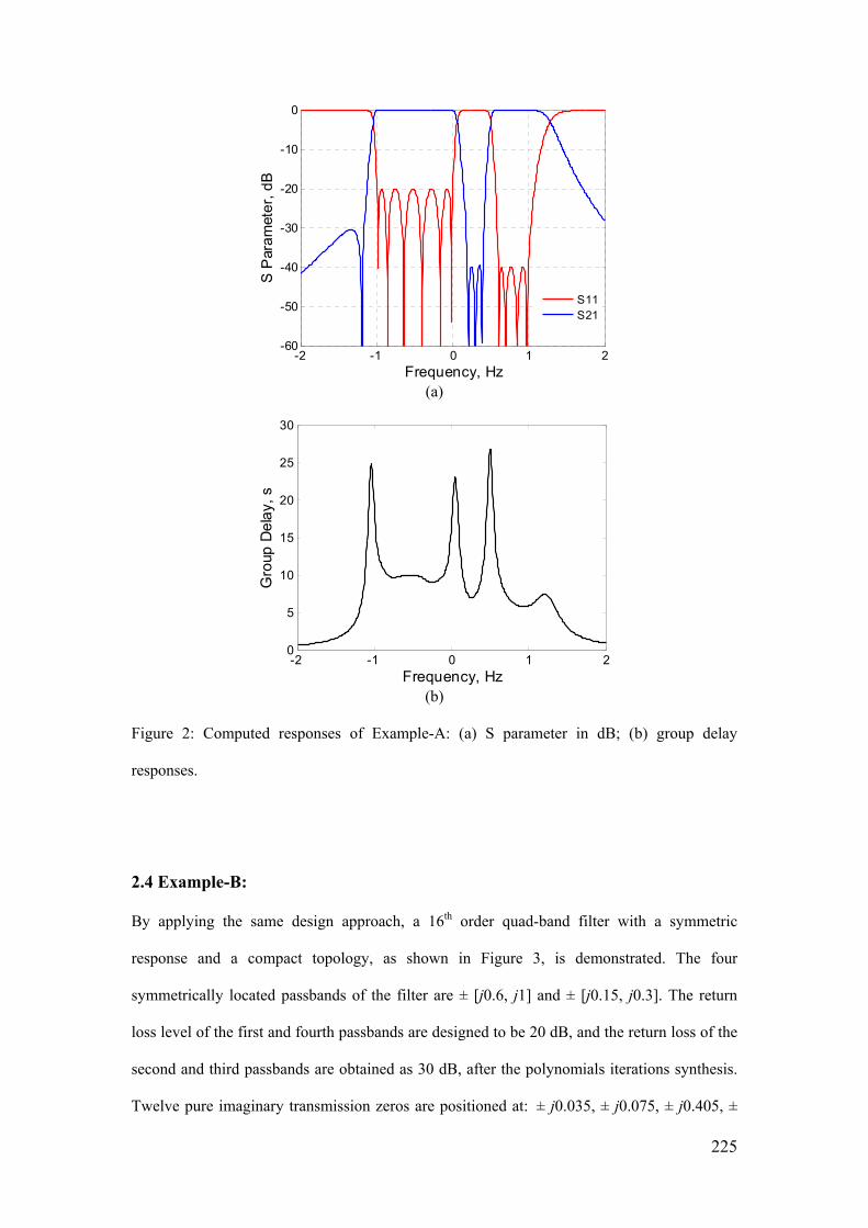
225
(a)
(b)
Figure 2: Computed responses of Example-A: (a) S parameter in dB; (b) group delay
responses.
2.4 Example-B:
By applying the same design approach, a 16th order quad-band filter with a symmetric
response and a compact topology, as shown in Figure 3, is demonstrated. The four
symmetrically located passbands of the filter are ± [j0.6, j1] and ± [j0.15, j0.3]. The return
loss level of the first and fourth passbands are designed to be 20 dB, and the return loss of the
second and third passbands are obtained as 30 dB, after the polynomials iterations synthesis.
Twelve pure imaginary transmission zeros are positioned at: ± j0.035, ± j0.075, ± j0.405, ±
-2 -1 0 1 2-60
-50
-40
-30
-20
-10
0
Frequency, Hz
S P
ara
met
er,
dB
S11S21
-2 -1 0 1 20
5
10
15
20
25
30
Frequency, Hz
Gro
up D
ela
y, s

226
j0.45, ± j0.495, ± j1.5 to separate different passbands. After coupling matrix optimisation the
resultant coupling coefficients (non-zero values) and calculated external quality factors are
shown below. Their corresponding S parameter responses at normalized frequency are given
in Figure 4.
Port1 Port2
4 5 12 13
3 6 11 14
2 7 10 15
1 8 9 16
Figure 3: Topology of Example-B
Figure 4: Computed responses of Example-B.
qe1=qe16=1.5327, m12=-0.7406, m23=0.2817, m34=-0.1649, m45=0.0189, m56=-0.3334,
m67=0.3436, m78=-0.5646, m89=0.2166, m9,10=0.6948, m10,11=0.291, m11,12=0.325,
m12,13=0.122, m13,14=0.1277, m14,15=0.2181, m15,16=-0.4768, m18=0.2021, m27=0.346, m36=-
0.2469, m5,12=0.2348, m6,11=0.1366, m7,10=0.43, m9,16=-0.6016, m10,15=-0.0515, m11,14=-0.3589.
The time needed for each design of the above two examples is less than 5 minutes on a
personal computer with a processor with 2.66 GHz clock speed and 2 GB of RAM. The
majority of the time has been spent by GA optimisation to find the proper initial value for the
followed SQP local optimisation procedure. It is worth pointing out that, to demonstrate the
-2 -1.5 -1 -0.5 0 0.5 1 1.5 2
-70
-60
-50
-40
-30
-20
-10
0
Frequency, Hz
S P
ara
me
ter,
dB
S21S11

227
advantages of the cost function (i.e. equation 3) proposed in this work, the cost function in [6]
has also been attempted to acquire the desired coupling matrices of Examples A and B using
the hybrid optimisation algorithm. However, the optimisation failed to converge in a
reasonable time for both examples. As mentioned in Section 2.2, the program may converge
to the desired solutions by altering the weighting functions of each terms of the cost function
in [6].
3 Experimental verifications
The coupling matrix of an 8th order dual-band filter has been obtained using above
optimisation method and realized using waveguide technology to verify this design approach.
This dual-band filter is designed to operate at a centre frequency of 10 GHz with two
symmetrically located passbands of 9.35 - 9.70 GHz and 10.30 - 10.65 GHz. The attenuation
at the stopband is designed to be 45 dB and achieved by introducing two transmission zeros
occur at 9.88 GHz and 10.12 GHz. The return loss of both passbands is 20 dB. The topology
of the filter is shown in Figure 5 (a). After getting the characteristic polynomials of the low-
pass prototype which fulfil the filter specifications, optimisation was performed to generate
the coupling matrix. The non-zero values of the coupling matrix after optimisation and
calculated external quality factor are: qe1 = qe8 =1.7278, m12=m78=0.6452, m23=m67=0.0476,
m34=m56=0.6623, m45=0.3786, m14=m58=-0.5389. The normalized coupling matrix of the low-
pass prototype is transformed to the real frequency domain, giving: Qe1=Qe8=13.2908,
M12=M78=0.0840, M23=M67=0.0062, M34=M56=0.0862, M45=0.0493, M14=M58=-0.0702. Their
corresponding prototype S parameter responses are shown in Figure 6. The approach in [23]
has been followed to acquire physical dimensions of this dual-band filter from these external
quality factor and coupling coefficients values.

228
It should be noted that the cross couplings M14 and M58 have a negative sign as opposite to
other coupling coefficients. Normally in a rectangular waveguide these different signs are
achieved by using different coupling irises (i.e. capacitive or inductive irises). In this paper,
the coupling irises used are exclusively capacitive, which makes the required negative
coupling more difficult to realise. As shown in Figure 5 (b), the negative couplings M14, M58
are achieved by employing two TE102 mode cavities 1 and 8, whereas the remaining six
cavities operate with TE101 mode. A similar principle has been used in [25] but in this case it
is for all inductive coupling irises. The two desired features for this kind of structure are:
firstly, it is easy for CNC (Computer Numerical Control) milling, since only two simple
identical parts need to be fabricated and assembled. A good insertion loss can be achieved
using the E-plane split configuration. Secondly, this all-capacitive-iris split-block structure is
compatible with the multi-layer micromachining technology that has been developed for
fabricating millimetre-wave components [26]. It is planned that the current design will be
scaled to 300 GHz and fabricated using this layered micromachining technology.
(a)
(b)
Figure 5: (a) Topology of the designed dual-band filter. (b) A photograph of one half of the
eighth-order symmetrical dual-band waveguide filter with tuning screw holes, b=10.16 mm.
The first and eighth cavities operate at TE102 mode while the rest resonators operate at
conventional TE101 mode.

229
There are drawbacks of this all-capacitive coupling structure. It is not suitable for filters
containing small couplings. As the capacitive iris itself is a section of propagating waveguide,
it causes a relatively strong coupling even with small gaps [27]. Additionally, compared with
an inductive-iris filter, filters with capacitive irises have a higher rejection in the upper
stopband, but a lower rejection in the frequency range close to the cut-off of the feeding
waveguide [28]. Since the capacitive irises are in fact resonant irises with their resonance
frequency centred at TE10 mode cut-off [29]. This results in the poorer-than-theory rejection
at lower stopband, as shown in Figure 6 (b). Additionally, standard X-band waveguide
resonator filters often suffer from poor higher stopband behaviour due to the appearance of
higher order modes and the resonances at higher harmonic frequencies, which occur at
frequencies of 1.6 to 1.7 times the centre frequency. For the X-band filter presented in this
paper, situation becomes worse since an extra resonance at 12.46 GHz introduced by the first
and eighth cavity operating at the unwanted TE103 mode was generated. This leads to the
worse-than-theory attenuation performance at the upper stopband, as shown in Figure 6 (b).
The input/output of the filter is a WR-90 rectangular waveguide interface. The pieces were
machined from copper. The measured response before tuning was slightly shifted to higher
frequencies. It was identified that this shift was due to the round corners (with a radius of 1.6
mm) of each resonator, which was not taken into account in the design. After adding tuning
screws to the resonators and coupling irises, the frequency shift was corrected and the
measurement result showed excellent agreement with the simulation as in Figure 6.

230
(a)
(b)
Figure 6: The symmetrical dual-band filter performance obtained from prototype coupling
matrix (i.e. ideal responses), CST simulation and the measurement after tuning. (a) S11 in dB.
(b) S21 in dB.
4 Conclusions
This paper presents a coupling matrix design procedure based on a hybrid optimisation
algorithm which can be applied to cross-coupled multi-band filters having specified, diverse
topologies and responses. The characteristic polynomials fulfil the filter specifications are
generated by an iterative design technique based on polynomial fit. This iterative synthesis
8.5 9 9.5 10 10.5 11 11.5-50
-40
-30
-20
-10
0
Frequency, GHz
S1
1,
dB
Simulated
Measured
Ideal
8.5 9 9.5 10 10.5 11 11.5-80
-70
-60
-50
-40
-30
-20
-10
0
Frequency, GHz
S2
1,
dB
SimulatedMeasuredIdeal

231
method guaranteed convergence and is also able to generate polynomials for multi-band filter
with different return loss levels at each passband. After calculating the characteristic
polynomials, a hybrid optimisation technique is performed directly on the coupling matrix to
seek the optimal set of coupling coefficients. This hybrid optimisation technique employs a
GA to choose strong initial values for the following SQP search and was described in detail in
[6]. At each optimisation iteration, a novel and efficient cost function which measures the
difference of the frequency locations of reflection and transmission zeros is evaluated. This
cost function eliminates the need of weighting functions or searching. An equation to
calculate external quality factors from polynomials has been derived for filters with both
symmetrical and asymmetrical responses and presented in this paper. Coupling matrices for a
complex dual-band and quad-band filter with topologies which cannot be synthesised
analytically have been demonstrated as two examples. An X-band dual-band waveguide filter
has been designed, fabricated and measured to verify this design approach; and excellent
agreement between the simulation result and measured result has been demonstrated. A novel
technique to achieve both positive and negative couplings using the same kind of coupling
irises has been employed by the dual-band waveguide filter and presented.
5 Acknowledement
This work was supported in part by the U.K. Engineering and Physical Science Research
Council (EPSRC), and by a fellowship from the Automatic RF Techniques Group. Many
constructive suggestions by reviews of this paper are also greatly appreciated.
6 References [1] Atia W. A., Zaki. K. A, and Atia A. E.: ‘Synthesis of General Topology Multiple Coupled
Resonator Filters by Optimisation’, IEEE MTTS Int. Microw. Symp., Baltimore, USA, June
1998, pp. 821-824

232
[2] Amari S.: ‘Synthesis of Cross-Coupled Resonator Filters Using an Analytical Gradient-
based Optimisation Technique’, IEEE Trans. Microw. Theory Tech., 2000, 48, (9), pp. 1559–
1564
[3] Mokhtaari M., Borenemann J., Rambabu K., Amari S.: ‘Coupling Matrix Design of Dual
and Triple Passband Filters’, IEEE Trans. Microw. Theory Tech., 2006, 54, (11), pp.3940-
3946
[4] Amari S., Rosenberg U., and Bornemann J.: ‘Adaptive Synthesis and Design of Resonator
Filters With Souce/Load-Multiresonator Coupling’, IEEE Trans. Microw. Theory Tech., 2002,
50, (8), pp.1969-1978
[5] Jayyousi A.B., Lancaster M. J.: ‘A Gradient-based Optimisation Technique Employing
Determinants for the Synthesis of Microwave Coupled Filters’, IEEE MTTS Int. Microw.
Symp., Fort Worth, USA, June 2004, pp. 1369-1372
[6] Nicholson G.L., Lancaster M. J.: ‘Coupling Matrix Synthesis of Cross-coupled
Microwave Filters using a Hybrid Optimisation Algorithm’, IET Microw. Antennas Propaga.,
2009, 3, (6), pp. 950-958
[7] Bell H.C.: ‘Canonical Asymmetric Coupled-Resonator Filter’, IEEE Trans. Microw.
Theory, 1982, 30, (9), pp.1335-1340
[8] Cameron R.J.: ‘General Coupling Matrix Synthesis Methods for Chebyshev Filtering
Functions’, IEEE Trans. Microw. Theory Tech., 1999, 47, (4), pp. 433–442
[9] Cameron R.J.: ‘Advanced Coupling Matrix Synthesis Techniques for Microwave Filters,’
IEEE Trans. Microw. Theory, 2003, 51, (1), pp. 1-10
[10] Macchiarella G.: ‘Accurate Synthesis of In-Line Prototype Filters using Cascaded Triplet
and Quadruplet Sections’, IEEE Trans. Microw. Theory Tech., 2002, 50, (7), pp. 1779-1783
[11] Tamiazzo S., Macchiarella G.: ‘ An Analytical Technique for the Synthesis of Cascaded
N-Tuplets Cross-Coupled Resonator Microwave Filters Using Matrix Rotations’, IEEE Trans.
Microw. Theory Tech., 2005, 53, (5), pp. 1693-1698
[12] Lee J., Uhm M. S., Yorn I. B.: ‘A Dual-Passband Filter of Canonical Structure for
Satellite Application”, IEEE Microw. Wireless Compt. Letter, 2004
[13] Lenoir P., Bila S., Seyfert F., etc: ‘Synthesis and Design of Asymmetrical Dual-Band
Bandpass Filters Based on Equivalent Network Simplification’, IEEE Trans. Microw. Theory
Tech., 2006, 54, (7), pp. 3090-3097.
[14] Macchiarella G., Tamiazzo S.: ‘A Design Technique for Symmetric Dual-Band Filters’,
IEEE MTTS Int. Microw. Symp., 2005, pp. 115-118
[15] Macchiarella G., Tamiazzo S.: ‘Design Technique for Dual-Passband Filters’, IEEE
Trans. Microw. Theory Tech., 2005, 53, (11), pp.3265-3271
[16] Lee J., Sarabandi K.: ‘A Synthesis Method for Dual-Passband Microwave Filters’, IEEE
Trans. Microw. Theory Tech., 2007, 55, (6), pp.1163-1170

233
[17] Lee J., Sarabandi K.: ‘Design of Triple-Passband Microwave Filters Using Frequency
Transformations’, IEEE Trans. Microw. Theory Tech., 2008, 56, (1), pp.187-193
[18] Lamecki A., Kozakowski P., and Mrozowski M.: ‘Fast synthesis of coupled-resonator
filters’, IEEE Microw. Wireless Components Lett., 2004,14, (4), pp. 174-176
[19] Kozakowski P., Mrozowski M.: ‘Automated synthesis of coupled resonator filters with a
given topology’, 14th Int. Conf. Microw. Radar Wireless Communications, Gdansk, Poland,
May 2002, pp. 373–376
[20] McGee W.: ‘Numerical Approximation Technique for Filter Characteristic Functions’,
IEEE Trans. Microw. Theory Tech., 1967, 14, (1), pp.92-94
[21] Deslandes Dominic, Boone Francois: ‘Iterative Design Techniques for All-Pole Dual-
Bandpass Filters’, IEEE Microw. Wireless Components Lett., 2007,17, (11), pp. 775-777
[22] Deslandes Dominic, Boone Francois: ‘An Iterative Design Procedure for the Synthesis of
Generalized Dual-Bandpass Filters’, International Journal of RF and Microw. Computer-
aided Engineering, 2009, 19, (5), pp.607-614
[23] Hong J.-S., Lancaster M.J.: ‘Microstrip filters for RF/ microwave applications’ (Wiley-
Interscience, 2001)
[24] Atia A. E., Williams A. E.: ‘Narrow-Bandpass waveguide filters’, IEEE Trans. Microw.
Theory Tech., 1972, 20, (4), pp. 258-265
[25] Rosenberg U.: ‘New ‘Planar’ Waveguide cavity elliptic function filters’, Proc 25th Eur.
Microwave Conf., 1995, pp.524-527
[26] Wang Y., Ke M., Lancaster M. J.: ‘Micromachined 38GHz cavity resonator and filter
with rectangular-coaxial feed-lines’, IET Microw. Antennas Propag., 2009,3, (1), pp. 125-129
[27] Ruiz-Cruz J. A., Zaki K. A., Montejo-GArai J. R. and Rebollar J. M.: ‘ Rectangular
waveguide elliptic filters with capacitive and inductive irises and integrated coaxial
excitation’, IEEE MTTS Int. Microw. Symp. Digest, June 2005, pp. 269-272
[28] Rosenberg U., Amari S., and Bornemann J.: ‘Inline TM110- Mode filters with high-design
flexibility by utilizing bypass couplings of nonresonating TE10/01 modes’, IEEE Trans.
Microw. Theory Tech., 2003, 51, (6), pp. 1735-1742
[29] Craven G. F., Skedd R. F.: ‘Evanescent Mode Microwave Components’ (Artech House
Inc., 1987)
234
Coupling Matrix Synthesis of Triple-Passband Filters using Optimisation
Xiaobang Shang*1, Yi Wang*2, Michael J. Lancaster*3
*School of Electronic, Electrical and Computer Engineering, the University of Birmingham, B15 2TT, U.K.
Email: [email protected], [email protected], [email protected]
Summarized Paper
The design of dual- and triple-passband filters has been attracting more and more attenuation recently due to their increasing use in modern wireless and satellite systems. In this paper a design methodology based on numerical optimisation which is capable of synthesis triple-passband filters with diverse topologies has been presented. Generally the design procedure comprises two steps: the synthesis of the filter characteristic polynomial transfer functions which meet the filter specification, followed by the coupling matrix synthesis procedure.
For the polynomial synthesis, an iterative design procedure based on polynomial fit similar to the method used in [1-3] has been employed to obtain the desired responses of the filter which meets the specifications. The frequency locations of transmission zeros (i.e. sTzP), reflection zeros (i.e. sRzP) and poles (i.e. sPP) of the filter can be easily calculated from these polynomials.
After obtaining the ideal polynomial transfer functions, an optimisation procedure is carried out to acquire the coupling matrix of the filter. The optimisation is performed directly on the coupling matrix and a Genetic algorithm (GA) is employed to generate strong initial values for the control variables for a local optimisation algorithm-Sequential Quadratic Programming (SQR) search. A fast and efficient cost function which measures the difference of the frequency locations of zeros and poles between the response produced by the coupling matrix and the ideal response is employed, as shown in the following:
RzM RzP TzM TzP PM PP2 2 2
1 1 1
( ) ( ) ( ) ( ) ( ) ( ) ( )N NT N
i i i
C s i s i s i s i s i s i
x (1)
where sRzM, sTzM and sPM are the frequency locations of the reflection and transmission zeros and the poles calculated from the coupling matrix. The vector variable x stands for the set of control variables at the current optimisation iteration, i.e. the coupling coefficients. This novel cost function is beneficial to accelerate the optimisation process.
The efficiency of numerical methods employing local optimisation algorithms depends highly on the quality of the initial value. A genetic algorithm is able to solve this problem by virtue of its global optimisation capability, however, in some case the genetic algorithm may be considered inefficient since it may suffers from slow convergence and lack accuracy in the final solution. Therefore, in this paper a GA and a local search algorithm has been combined to overcome their shortcomings. Convergence of the optimisation is proved to be fast and no initial values for the control parameters are required. In the following the coupling matrix synthesis of two exemplar filters has been presented.
Example-1: 16th order symmetrical triple-band filter with 8 transmission zeros
A coupling matrix for a 16th order symmetrical triple-band filter with a cascaded-quadruplet topology as shown in Fig.1 (a) was produced using the optimisation described above. The three passbands of the filter are [-1 -0.6], [-0.3 0.3] and [0.6 1]. The return loss of the first/third passband is 20 dB and the return loss for the second band has been chosen to be 30 dB. It should be pointed out that the return loss of the second passband can be adjusted to fit the required specification by altering the positions of transmission zeros and number of resonators of each passband. Equal return loss level at all passbands is just one special case and is easily achievable. After optimisation the non-zero elements of the resultant coupling matrix and external quality factors are show below and the corresponding responses at normalized frequency are given in Fig. 2(a).
qe1=qe16=1.2243, m12=0.328, m23=0.3619,m34=0.0851,m45=0.6119,m56=-0.2991,m67=-0.4906, m78 = 0.0662, m89=-0.635,m910=0.3626,m1011=0.3632, m1112=-0.0778,m1213=0.6,m1314=0.004,m1415=-0.6, m1516 = 0.418, m14=0.6738,m36=-0.309,m58=0.2792,m710=-0.3272, m912=0.2292, m1114=0.6991, m1316=0.622.

235
Example-2: 10th order asymmetrical triple-band filter with 6 transmission zeros
A coupling matrix for a 10th order asymmetrical triple-band filter with a canonical topology as shown in Fig.1 (b) was generated using the same optimisation approach. The three passbands of the filter are [-1 -0.4], [0 0.3] and [0.78 1]. The return loss of the three passbands is 20 dB. The coupling coefficients after optimisation and external quality factors are given below and the responses are shown in Fig. 2(b).
qe1=qe10=1.6594, m12=0.7386,m23=0.5615,m34=0.4399,m45=0.3614,m56=-0.1941,m67=0.3552,m78=-0.4623 , m89=-0.5623,,m910=-0.7386,m11=-0.138,m22=0.0655,m33=-0.0264, m44=0.0177, m55=0.208, m66=0.3104, m77=-0.0677,m88=0.0057,m99=0.0655,m1010=-0.138, m29=0.1025, m28=0.0287, m38=0.3146, m37=0.1677, m47=-0.1304,m46=-0.2116.
Fig.1 : (a) Topology of Example-1; (b) Topology of Example-2
Fig.2: Frequency responses at normalized frequency (a) Example-1; (b) Example-2
Conclusions In this paper a coupling matrix synthesis procedure based on optimisation which may be applied to cross-coupled microwave filters having diverse topologies and responses has been presented. For demonstration coupling matrices of two triple-band filters have been extracted using this optimisation procedure. Convergence of the optimisation is fast and no initial values for control parameters are required. The coupling matrix of other multiple-passband filter can also be obtained using the same design technique.
References [1] McGee W.: ‘Numerical Approximation Technique for Filter Characteristic Functions’, IEEE Trans.
Microw. Theory Tech., 1967, 14, (1), pp.92-94
[2] Deslandes Dominic, Boone Francois: ‘Iterative Design Techniques for All-Pole Dual-Bandpass Filters’,
IEEE Microw. Wireless Components Lett., 2007,17, (11), pp. 775-777
[3] Deslandes Dominic, Boone Francois: ‘An Iterative Design Procedure for the Synthesis of Generalized
Dual-Bandpass Filters’, International Journal of RF and Microw. Computer-aided Engineering, 2009, 19,
(5), pp.607-614