readout techniques for high-q micromachined vibratory … · readout techniques for high-q...
TRANSCRIPT
Readout Techniques for High-Q MicromachinedVibratory Rate Gyroscopes
Chinwuba David Ezekwe
Electrical Engineering and Computer SciencesUniversity of California at Berkeley
Technical Report No. UCB/EECS-2007-176
http://www.eecs.berkeley.edu/Pubs/TechRpts/2007/EECS-2007-176.html
December 21, 2007

Copyright © 2007, by the author(s).All rights reserved.
Permission to make digital or hard copies of all or part of this work forpersonal or classroom use is granted without fee provided that copies arenot made or distributed for profit or commercial advantage and that copiesbear this notice and the full citation on the first page. To copy otherwise, torepublish, to post on servers or to redistribute to lists, requires prior specificpermission.
Readout Techniques for High-Q Micromachined Vibratory RateGyroscopes
by
Chinwuba David Ezekwe
B.S. (University of California, Berkeley) 2000
A dissertation submitted in partial satisfactionof the requirements for the degree of
Doctor of Philosophy
in
Engineering - Electrical Engineering and Computer Sciences
in the
GRADUATE DIVISION
of the
UNIVERSITY OF CALIFORNIA, BERKELEY
Committee in charge:
Professor Bernhard E. Boser, ChairProfessor Kristofer S. J. Pister
Professor Roberto Horowitz
Fall 2007
The dissertation of Chinwuba David Ezekwe is approved.
Chair Date
Date
Date
University of California, Berkeley
Fall 2007
Readout Techniques for High-Q Micromachined Vibratory Rate Gyroscopes
Copyright c© 2007
by
Chinwuba David Ezekwe
Abstract
Readout Techniques for High-Q Micromachined Vibratory Rate Gyroscopes
by
Chinwuba David Ezekwe
Doctor of Philosophy in Engineering - Electrical Engineering and Computer Sciences
University of California, Berkeley
Professor Bernhard E. Boser, Chair
Inexpensive MEMS gyroscopes are enabling a wide range of automotive and consumer
applications. Examples include image stabilization in cameras, game consoles, and
improving vehicle handling on challenging terrain. Many of these applications impose
very stringent requirements on power dissipation. For continued expansion into new
applications it is imperative to reduce power consumption of present devices by an
order-of-magnitude.
Gyroscopes infer angular rate from measuring the Coriolis force exerted on a
vibrating or rotating mass. For typical designs and inputs, this signal is extremely
small, requiring ultralow noise pickup electronic circuits. This low noise requirement
directly translates into excessive power dissipation.
This work describes a solution that combines a new low-power electronic readout
circuit with mechanical signal amplification using a technique called mode-matching.
The electronic circuit continuously senses the resonance frequency of the mechanical
sense element and electrically tunes it to maximize the output signal. A new and
robust feedback controller is used to accurately control the scaling factor and band-
width of the gyroscope while at the same time guaranteeing stability in the presence
of undesired parasitic resonances.
1

The circuit has been fabricated in a 0.35µm CMOS process and consumes less than
1mW. The spot noise is 0.004 /s/√
Hz.
Professor Bernhard E. BoserDissertation Committee Chair
2

To my late father.
i
Contents
Contents ii
Acknowledgements iv
1 Introduction 1
2 Power-Efficient Coriolis Sensing 4
2.1 Review of Vibratory Gyroscopes . . . . . . . . . . . . . . . . . . . . . 4
2.2 Electronic Interface . . . . . . . . . . . . . . . . . . . . . . . . . . . . 5
2.3 Readout Interface . . . . . . . . . . . . . . . . . . . . . . . . . . . . . 7
2.4 Improving Readout Interface Power Efficiency . . . . . . . . . . . . . 9
2.5 Exploiting the Sense Resonance . . . . . . . . . . . . . . . . . . . . . 11
3 Mode Matching 15
3.1 Estimating the Mismatch . . . . . . . . . . . . . . . . . . . . . . . . . 16
3.2 Tuning Out the Mismatch . . . . . . . . . . . . . . . . . . . . . . . . 21
3.3 Closing the Tuning Loop . . . . . . . . . . . . . . . . . . . . . . . . . 22
3.4 Practical Considerations . . . . . . . . . . . . . . . . . . . . . . . . . 24
3.4.1 Practical Signal Synthesis, Demodulation, and Filtering . . . . 24
3.4.2 Finite Force Feedback Open-Loop Gain . . . . . . . . . . . . . 27
3.4.3 Interference from Large Inertial Forces . . . . . . . . . . . . . 28
3.5 Summary . . . . . . . . . . . . . . . . . . . . . . . . . . . . . . . . . 30
4 Position Sensing 31
4.1 Force Feedback Loop Stability Consideration . . . . . . . . . . . . . . 31
4.2 Sampling and Noise Folding . . . . . . . . . . . . . . . . . . . . . . . 32
ii

4.3 Boxcar Sampling . . . . . . . . . . . . . . . . . . . . . . . . . . . . . 35
4.4 Removing Switch kT/C Noise and Amplifier 1/f Noise . . . . . . . . 39
4.5 Other Practical Considerations . . . . . . . . . . . . . . . . . . . . . 40
4.6 Summary . . . . . . . . . . . . . . . . . . . . . . . . . . . . . . . . . 43
5 Force Feedback 45
5.1 Mode-Matching Consideration . . . . . . . . . . . . . . . . . . . . . . 45
5.2 Preliminary System Architecture and Model for Stability Analysis . . 47
5.3 Accommodating Parasitic Resonances . . . . . . . . . . . . . . . . . . 48
5.3.1 Traditional Lead Compensation . . . . . . . . . . . . . . . . . 50
5.3.2 Positive Feedback Technique . . . . . . . . . . . . . . . . . . . 51
5.4 Positive Feedback Architecture . . . . . . . . . . . . . . . . . . . . . 55
5.4.1 Setting the Open-Loop DC Gain . . . . . . . . . . . . . . . . 55
5.4.2 Accommodating Sensor Offset . . . . . . . . . . . . . . . . . . 58
5.4.3 System Design . . . . . . . . . . . . . . . . . . . . . . . . . . 60
5.5 Summary . . . . . . . . . . . . . . . . . . . . . . . . . . . . . . . . . 63
6 An Experimental Readout Interface 65
6.1 Implementation . . . . . . . . . . . . . . . . . . . . . . . . . . . . . . 65
6.1.1 Front-End and 3-Bit DAC . . . . . . . . . . . . . . . . . . . . 67
6.1.2 Compensator . . . . . . . . . . . . . . . . . . . . . . . . . . . 68
6.2 Experimental Results . . . . . . . . . . . . . . . . . . . . . . . . . . . 72
6.3 Summary . . . . . . . . . . . . . . . . . . . . . . . . . . . . . . . . . 77
7 Conclusions 78
7.1 Results . . . . . . . . . . . . . . . . . . . . . . . . . . . . . . . . . . . 78
7.2 Future Work . . . . . . . . . . . . . . . . . . . . . . . . . . . . . . . . 79
Bibliography 80
iii
Acknowledgements
I would like to thank Professor Bernhard E. Boser for his continuing support, guidance
and encouragement and for giving me the independence to follow my ideas wherever
they led. His constant but constructive criticisms were key in the successful outcome
of this study. I would like to thank Professor Kristofer S. J. Pister for his continuing
support and guidance. He challenged me while I was an undergraduate, recommended
me for graduate study, and steered me in the direction most suited to my strengths.
I would also like to thank Professor Seth R. Sanders and Professor Steven D. Glaser
for listening to my ideas and providing me with useful feedback during my qualifying
examination and Professor Roberto Horowitz for reading my dissertation.
I conducted a major portion of this work at the Robert Bosch Research and Tech-
nology Center, where I had the benefit of receiving tremendous help from Christoph
Lang, Vladimir P. Petkov, Johan P. Vanderhaegen, Xinyu Xing and others, and Ger-
hard Schneider, who provided all necessary accommodations to facilitate my work at
Bosch. I extend special thanks to them all.
I thank my friends and colleagues in the Berkeley EECS department. Sarah
Bergbreiter, Baris Cagdaser, Octavian Florescu, Steven M. Lanzisera, Matthew E.
Last, Brian S. Leibowitz, Travis L. Massey, Ankur M. Mehta, Mike D. Scott, George
W. Shaw, Karl R. Skucha, Jason T. Stauth, Subramaniam Venkatraman, David Zats
and others in the department made my graduate school experience very enjoyable.
I thank Ruth Gjerde and Mary K. Byrnes in the Graduate Student Affairs offices
for their eagerness to extend help on numerous occasions.
I am very grateful to my wife for her love, support, encouragement, and under-
standing. Her sacrifice gave me the freedom to concentrate on, and complete, this
study. I am forever indebted to my late father, my mother, and my sister for their
many sacrifices. I thank my daughter for being patient with me while I was writing
this dissertation. I thank my and my wife’s extended family for their support.
This research was funded by Robert BOSCH LLC.
iv

v
Chapter 1
Introduction
Motion sensing is finding increasing application in various equipments such as
cameras that compensate for image blur caused by camera shake and vehicles that
prevent loss of control on sudden swerving by the driver. In the vehicle, as in the
camera, compensation for the undesired movement is enabled by a micromachined
angular rate sensor, a complex system consisting of a mechanical element that senses
the physical motion and electronic circuits that read out the motion.
While the application domain of micromachined angular rate sensors, or gyro-
scopes as they are commonly called, has continued to expand, for example into in-
ertial navigation and virtual reality, the power dissipation of the electronic circuits,
failing to keep pace with general improvements expected with each electronic device
generation, is becoming too prohibitive for present applications and is threatening the
emergence of new ones. Whether it is in the hand-held consumer electronics space
where battery life is the principal consideration or in the automotive arena where
the power dissipated and the consequent heat produced by the sensor cluster call
for expensive packaging and constrain the expansion of sensing capability, the power
dissipation of current state-of-the-art micromachined gyroscopes is quickly becoming
a limiting factor.
This work focuses on achieving the substantial improvements in power efficiency
essential for the continued expansion of micromachined gyroscopes into new applica-
tion. Proposed in this dissertation is a readout architecture which, with only a modest
1
increase in the complexity of the electronic circuits, exploits opportunities inherent in
the sensor and elsewhere to reduce power dissipation by orders-of-magnitude without
compromising any aspect of sensor performance.
After providing a brief review of vibratory gyroscopes, the most prevalent kind
of micromachined angular rate sensors, the next chapter begins consideration of the
electronics with particular emphasis on the readout interface. The chapter proposes
matching the drive and sense resonance modes of the sense element as a means to
substantially reduce power dissipation and further proposes force feedback as a means
to overcome the difficulties that have until now prevented the full exploitation of
mode-matching.
Full exploitation of mode-matching requires a level of frequency matching beyond
manufacturing limits. Chapter 3 introduces a resonance frequency calibration tech-
nique to overcome the limits imposed by manufacturing tolerances. Unlike previously
reported schemes, this technique continuously and automatically tunes the resonance
frequencies while the sense element is an active force feedback loop, avoiding costly
in-factory calibration.
Feedback generally relaxes the requirements of the blocks in the forward path.
Focusing on the position sense front-end, the block that dominates active power
dissipation, Chapter 4 proposes a front-end architecture that exploits the presence of
the front-end in the forward path of the force feedback to achieve additional reductions
in power dissipation.
Designing the force feedback loop in a way that is compatible with other aspects
of the proposed architecture is essential for the whole system to work. Chapter 5
focuses on the design of the force feedback loop with particular emphasis on preserving
analog simplicity while ensuring that the loop is compatible with the mode-matching
algorithm and the highly underdamped resonances of a vacuum packaged sensor.
The techniques discussed in Chapters 3, 4, and 5 are applied in Chapter 6 towards
the implementation of an experimental readout interface in a 0.35µm CMOS process.
The interface consumes less than 1mW and achieves a spot noise of 0.004 /s/√
Hz
over a 50Hz band.
2
The last chapter, Chapter 7, summarizes the main results of this work and con-
cludes with suggestions for future research.
3
Chapter 2
Power-Efficient Coriolis Sensing
After a brief review of the basic operating principle of vibratory gyroscopes, this
chapter focuses on the electronic interface in search of opportunities to lower its
power dissipation. The chapter proposes mode-matching as a means to reduce power
dissipation by orders of magnitude from the levels set by state-of-the-art interfaces
and presents the basic elements of a readout architecture that enables the effective
exploitation of the proposed means.
2.1 Review of Vibratory Gyroscopes
Figure 2.1 illustrates the basic operating principle of vibratory gyroscopes. A
proof mass suspended by springs to a frame is maintained in a steady-state oscilla-
tory motion along the drive axis. Rotation of the frame in the plane formed by the
drive and sense axes produces, along the sense axis, a Coriolis acceleration that is
proportional to the product of the drive velocity and the angular rate. If we express
the drive oscillation as xd = xd0 cos(ωdt) where xd0 and ωd are respectively the am-
plitude and angular frequency of the drive oscillation, then the Coriolis acceleration
4
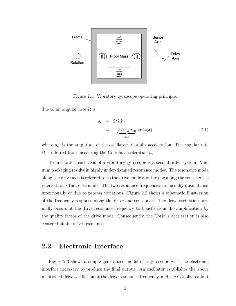
Drive
Axis
Sense
Axis
Proof Mass
Frame
Rotationdx
sx
Figure 2.1. Vibratory gyroscope operating principle.
due to an angular rate Ω is
ac = 2 Ω xd
= − 2 Ωωd xd0︸ ︷︷ ︸ac0
sin(ωdt) (2.1)
where ac0 is the amplitude of the oscillatory Coriolis acceleration. The angular rate
Ω is inferred from measuring the Coriolis acceleration ac.
To first order, each axis of a vibratory gyroscope is a second-order system. Vac-
uum packaging results in highly under-damped resonance modes. The resonance mode
along the drive axis is referred to as the drive mode and the one along the sense axis is
referred to as the sense mode. The two resonance frequencies are usually mismatched
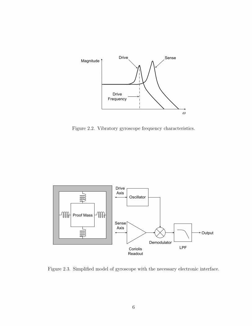
intentionally or due to process variations. Figure 2.2 shows a schematic illustration
of the frequency response along the drive and sense axes. The drive oscillation nor-
mally occurs at the drive resonance frequency to benefit from the amplification by
the quality factor of the drive mode. Consequently, the Coriolis acceleration is also
centered at the drive resonance.
2.2 Electronic Interface
Figure 2.3 shows a simple generalized model of a gyroscope with the electronic
interface necessary to produce the final output. An oscillator establishes the above
mentioned drive oscillation at the drive resonance frequency, and the Coriolis readout
5
Drive Sense
Drive
Frequency
Magnitude
ω
Figure 2.2. Vibratory gyroscope frequency characteristics.
Proof Mass
Oscillator
Drive
Axis
Sense
Axis
Demodulator
Coriolis
Readout
LPF
Output
Figure 2.3. Simplified model of gyroscope with the necessary electronic interface.
6
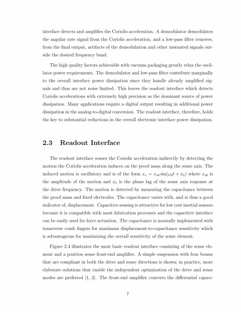
interface detects and amplifies the Coriolis acceleration. A demodulator demodulates
the angular rate signal from the Coriolis acceleration, and a low-pass filter removes,
from the final output, artifacts of the demodulation and other unwanted signals out-
side the desired frequency band.
The high quality factors achievable with vacuum packaging greatly relax the oscil-
lator power requirements. The demodulator and low-pass filter contribute marginally
to the overall interface power dissipation since they handle already amplified sig-
nals and thus are not noise limited. This leaves the readout interface which detects
Coriolis accelerations with extremely high precision as the dominant source of power
dissipation. Many applications require a digital output resulting in additional power
dissipation in the analog-to-digital conversion. The readout interface, therefore, holds
the key to substantial reductions in the overall electronic interface power dissipation.
2.3 Readout Interface
The readout interface senses the Coriolis acceleration indirectly by detecting the
motion the Coriolis acceleration induces on the proof mass along the sense axis. The
induced motion is oscillatory and is of the form xs = xs0 sin(ωdt + φs) where xs0 is
the amplitude of the motion and φs is the phase lag of the sense axis response at
the drive frequency. The motion is detected by measuring the capacitance between
the proof mass and fixed electrodes. The capacitance varies with, and is thus a good
indicator of, displacement. Capacitive sensing is attractive for low cost inertial sensors
because it is compatible with most fabrication processes and the capacitive interface
can be easily used for force actuation. The capacitance is normally implemented with
transverse comb fingers for maximum displacement-to-capacitance sensitivity which
is advantageous for maximizing the overall sensitivity of the sense element.
Figure 2.4 illustrates the most basic readout interface consisting of the sense ele-
ment and a position sense front-end amplifier. A simple suspension with four beams
that are compliant in both the drive and sense directions is shown; in practice, more
elaborate solutions that enable the independent optimization of the drive and sense
modes are preferred [1, 2]. The front-end amplifier converts the differential capaci-
7
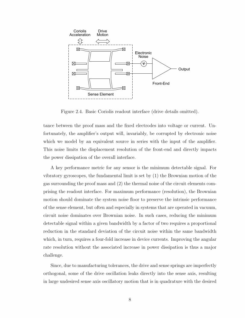
Sense Element
CoriolisAcceleration
DriveMotion
Output
ElectronicNoise
Front-End
Figure 2.4. Basic Coriolis readout interface (drive details omitted).
tance between the proof mass and the fixed electrodes into voltage or current. Un-
fortunately, the amplifier’s output will, invariably, be corrupted by electronic noise
which we model by an equivalent source in series with the input of the amplifier.
This noise limits the displacement resolution of the front-end and directly impacts
the power dissipation of the overall interface.
A key performance metric for any sensor is the minimum detectable signal. For
vibratory gyroscopes, the fundamental limit is set by (1) the Brownian motion of the
gas surrounding the proof mass and (2) the thermal noise of the circuit elements com-
prising the readout interface. For maximum performance (resolution), the Brownian
motion should dominate the system noise floor to preserve the intrinsic performance
of the sense element, but often and especially in systems that are operated in vacuum,
circuit noise dominates over Brownian noise. In such cases, reducing the minimum
detectable signal within a given bandwidth by a factor of two requires a proportional
reduction in the standard deviation of the circuit noise within the same bandwidth
which, in turn, requires a four-fold increase in device currents. Improving the angular
rate resolution without the associated increase in power dissipation is thus a major
challenge.
Since, due to manufacturing tolerances, the drive and sense springs are imperfectly
orthogonal, some of the drive oscillation leaks directly into the sense axis, resulting
in large undesired sense axis oscillatory motion that is in quadrature with the desired
8
Coriolis acceleration induced motion. The demodulation signal from the oscillator
circuit normally has substantial phase noise which the so called quadrature error can
mix down reciprocally, raising the overall interface noise floor beyond that set by the
front-end. Fortunately, most but not all of the quadrature error can be nulled using
special quadrature nulling electrodes [3]. The residual error can be rejected during
the demodulation process by using an appropriately phased demodulation signal since
the error is in quadrature with the desired signal. Achieving a high degree of rejection
requires a well defined phase relationship between the quadrature error and the drive
oscillation from which the demodulation signal is normally derived. Ensuring that the
phase relationship is well defined is the second significant challenge for the readout
interface.
There is also the Coriolis offset which comes from leakage of the drive force into
the sense axis due to misalignment of the drive combs. This error is minimized by
vacuum packaging since the increased quality factors enable the use of smaller drive
forces which result in smaller forces feeding through to the sense axis [4].
Other challenges include obtaining a wide enough signal bandwidth and ensuring
that the overall gain (scale factor) is stable over fabrication tolerances and ambient
variations. A wide bandwidth is necessary especially in control applications such as
vehicle stability control where sensors with minimum phase lag are required.
2.4 Improving Readout Interface Power Efficiency
In a vibratory gyroscope, rotation is converted to Coriolis acceleration that is
detected by measuring the consequent motion of the proof mass. A “rate grade”
resolution of 0.1 /s/√
Hz translates into a displacement resolution on the order of
100 fm/√
Hz in typical gyroscope designs. Current state-of-the art interfaces resolve
60 fm/√
Hz while dissipating 30 mW [2]. Applications such as image stabilization in
cameras and vehicle stability control require an order of magnitude better angular
rate resolution for similar or lower power dissipation. Unfortunately, power dissipa-
tion in a noise limited readout interface is, to first order, inversely proportional to
the square of the displacement resolution. Thus, while 0.01 /s/√
Hz can be achieved
9
through traditional means by simply resolving 10 fm/√
Hz, the 1 W of power required
makes such a noise floor impractical in the target applications. Essentially, the read-
out interface power efficiency must be improved to enable the use of high-resolution
angular rate sensors in power constrained applications. Increasing the signal-to-noise
ratio (SNR) passively requires increasing the sense element’s angular rate-to-sense
motion sensitivity (∆xs0/∆Ω) so that the same angular rate produces a larger sense
motion amplitude.
The angular rate-to-sense motion sensitivity can be expressed as the product of
two factors:∆xs0∆Ω
=
(∆ac0∆Ω
)(∆xs0∆ac0
). (2.2)
The first factor is the angular rate-to-Coriolis acceleration sensitivity which indicates
the amplitude of the Coriolis acceleration produced by a given angular rate. This
factor is normally maximized by a large drive oscillation amplitude. The second
factor is the Coriolis acceleration-to-sense motion sensitivity which indicates the sense
motion amplitude resulting from a given Coriolis acceleration amplitude. The drive
and sense resonance frequencies are normally mismatched either by design or due
to fabrication tolerances and ambient variations. However, if they were perfectly
matched, the Coriolis acceleration would be centered at the sense mode frequency,
and because of the consequent amplification by the sense mode quality factor, the
same Coriolis acceleration, and consequently the same angular rate, would produce a
much larger sense motion [5]. Continuing with the previous example and assuming a
ten fold increase in Coriolis acceleration-to-sense motion sensitivity, an angular rate
resolution of 0.01 /s/√
Hz would require a displacement resolution on the order of
100 fm/√
Hz rather than the more stringent 10 fm/√
Hz, which translates into two
orders of magnitude power dissipation reduction over the original example.
Based on the foregoing discussion, we propose to exploit the free mechanical am-
plification provided by the sense resonance to greatly relax the noise requirements,
and therefore substantially reduce the power dissipation, of the readout interface.
10
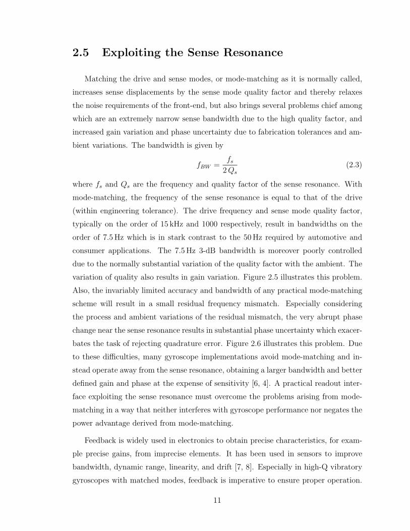
2.5 Exploiting the Sense Resonance
Matching the drive and sense modes, or mode-matching as it is normally called,
increases sense displacements by the sense mode quality factor and thereby relaxes
the noise requirements of the front-end, but also brings several problems chief among
which are an extremely narrow sense bandwidth due to the high quality factor, and
increased gain variation and phase uncertainty due to fabrication tolerances and am-
bient variations. The bandwidth is given by
fBW =fs
2Qs
(2.3)
where fs and Qs are the frequency and quality factor of the sense resonance. With
mode-matching, the frequency of the sense resonance is equal to that of the drive
(within engineering tolerance). The drive frequency and sense mode quality factor,
typically on the order of 15 kHz and 1000 respectively, result in bandwidths on the
order of 7.5 Hz which is in stark contrast to the 50 Hz required by automotive and
consumer applications. The 7.5 Hz 3-dB bandwidth is moreover poorly controlled
due to the normally substantial variation of the quality factor with the ambient. The
variation of quality also results in gain variation. Figure 2.5 illustrates this problem.
Also, the invariably limited accuracy and bandwidth of any practical mode-matching
scheme will result in a small residual frequency mismatch. Especially considering
the process and ambient variations of the residual mismatch, the very abrupt phase
change near the sense resonance results in substantial phase uncertainty which exacer-
bates the task of rejecting quadrature error. Figure 2.6 illustrates this problem. Due
to these difficulties, many gyroscope implementations avoid mode-matching and in-
stead operate away from the sense resonance, obtaining a larger bandwidth and better
defined gain and phase at the expense of sensitivity [6, 4]. A practical readout inter-
face exploiting the sense resonance must overcome the problems arising from mode-
matching in a way that neither interferes with gyroscope performance nor negates the
power advantage derived from mode-matching.
Feedback is widely used in electronics to obtain precise characteristics, for exam-
ple precise gains, from imprecise elements. It has been used in sensors to improve
bandwidth, dynamic range, linearity, and drift [7, 8]. Especially in high-Q vibratory
gyroscopes with matched modes, feedback is imperative to ensure proper operation.
11
GainVariation
0°
-90°
-180°
Phase
Magnitude
DriveFrequency
ω
ω
Figure 2.5. Gain (scale factor) variation with quality factor.
GainVariation
0°
-90°
-180°
Phase
Magnitude
ResidualMismatch
PhaseVariation
DriveFrequency
ω
ω
Figure 2.6. Gain and phase variation with residual mismatch.
12
SenseDynamics
Front-End
Compensator Output
ForceTransducer
Input
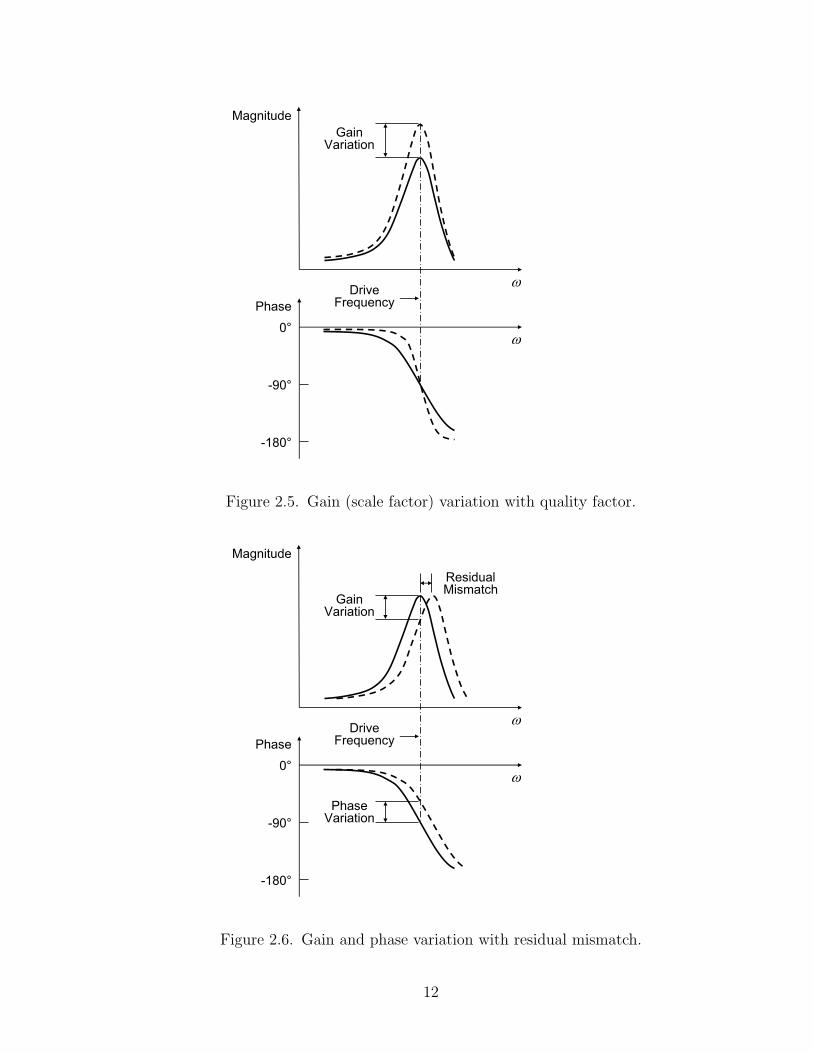
Figure 2.7. Basic force feedback loop.
Figure 2.7 shows the sense element enclosed in a force feedback loop. A compen-
sator and a force transducer are added to the basic open-loop interface to form a
closed-loop interface. Based on the motion sensed by the front-end, the compensator
produces an estimate of the Coriolis force which the force transducer applies with
opposite polarity on the proof mass to null the sense motion. Perfect nulling of the
proof mass motion implies that the feedback force is exactly equal and opposite to
the Coriolis force. While this is impossible to achieve over all frequencies in prac-
tice, adequate nulling is possible within a limited frequency band where the force
feedback open-loop gain is sufficiently high. Within that frequency band, the output
of the closed-loop interface is an accurate representation of the Coriolis acceleration.
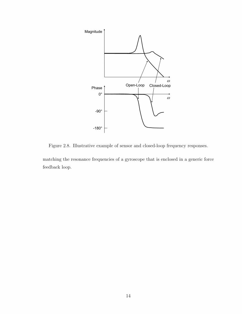
Figure 2.8 compares the frequency responses of the open-loop sensor and that of a
closed-loop interface that has a high open-loop gain over a frequency range that ex-
tends beyond the resonance of the sense element. Electronic circuits implementing
the compensator provide the necessary open-loop gain. Regardless of the variations of
the sensor parameters, the closed-loop response remains flat and stable over a much
wider frequency range. Thus, the traditional tradeoff of mechanical sensitivity for
larger bandwidth and better defined gain and phase is unnecessary.
With force feedback, the sense resonance can be fully exploited without sacri-
ficing other important aspects of system performance. However, successful use of
the closed-loop architecture depends on key implementation details. The next three
chapters further develop the architecture to address various details ignored by the
simple discussion presented so far. Leaving the problem of force feedback loop design
aside for a later chapter, the next chapter focuses on the problem of automatically
13
0°
-90°
-180°
Phase
Magnitude
Open-Loop Closed-Loop
ω
ω
Figure 2.8. Illustrative example of sensor and closed-loop frequency responses.
matching the resonance frequencies of a gyroscope that is enclosed in a generic force
feedback loop.
14

Chapter 3
Mode Matching
As argued in the previous chapter, matching the resonance frequencies of the
drive and sense modes amplifies the sense displacement and hence has the potential
to reduce the power dissipation of the readout interface. Maximizing the signal-to-
noise ratio (SNR) improvement requires the frequency matching error to be less than
the reciprocal of the sense mode quality factor. For example, a sense mode quality
factor of 1000 requires less than 0.1% matching error. Process tolerances and ambient
variations limit the minimum matching error achievable with precision manufacturing
to about 2% [4], mandating resonance frequency calibration.
One way to perform the calibration is to fully characterize the dependence of fre-
quency matching on physical parameters such as temperature and then use the data
to calibrate the sense resonance frequency at runtime. Besides the added complexity
of integrating additional sensors to measure the influential physical parameters, the
high cost of fully characterizing the sense element at the factory puts this technique
at odds with the cost constraints of MEMS gyroscope applications. The alternative
and preferred way is to monitor sensor properties that vary with frequency matching.
Previously proposed calibration schemes using the preferred approach determine fre-
quency matching by monitoring sensor properties such as gain and phase lag [1, 9].
Unfortunately, those properties are not easily measurable when the sense element is
part of a force feedback loop. Since force feedback is imperative to ensure proper
15
s
1
sb
s
1
sm
1 sx&&
sx&
sx
sF
sk
sF
sx( )sH
s
sk
Figure 3.1. Second-order sense dynamics with variable stiffness.
operation of a mode matched gyroscope, we need to develop a way to measure the
relevant sensor properties in a way that is compatible with closed-loop sensing.
3.1 Estimating the Mismatch
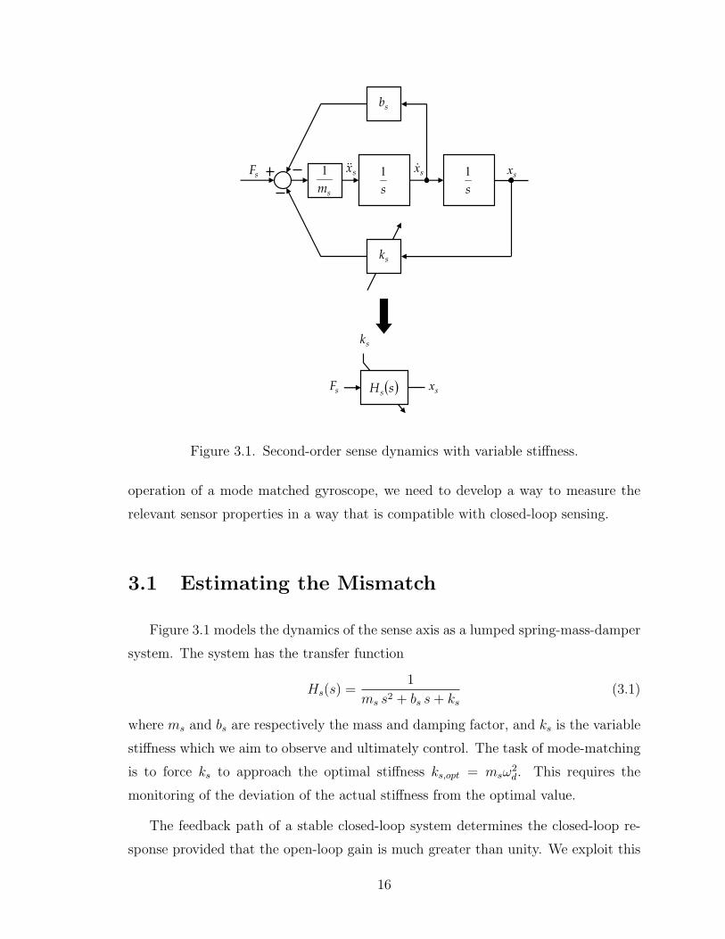
Figure 3.1 models the dynamics of the sense axis as a lumped spring-mass-damper
system. The system has the transfer function
Hs(s) =1
ms s2 + bs s+ ks(3.1)
where ms and bs are respectively the mass and damping factor, and ks is the variable
stiffness which we aim to observe and ultimately control. The task of mode-matching
is to force ks to approach the optimal stiffness ks,opt = msω2d. This requires the
monitoring of the deviation of the actual stiffness from the optimal value.
The feedback path of a stable closed-loop system determines the closed-loop re-
sponse provided that the open-loop gain is much greater than unity. We exploit this
16
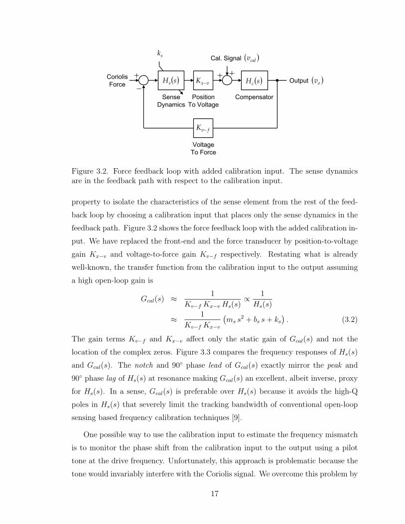
OutputCoriolis
Force
Cal. Signal
Position
To Voltage
Sense
Dynamics
Compensator
vxK −( )sHs ( )sHc
Voltage
To Force
fvK −
( )calv
( )ov
sk
Figure 3.2. Force feedback loop with added calibration input. The sense dynamicsare in the feedback path with respect to the calibration input.
property to isolate the characteristics of the sense element from the rest of the feed-
back loop by choosing a calibration input that places only the sense dynamics in the
feedback path. Figure 3.2 shows the force feedback loop with the added calibration in-
put. We have replaced the front-end and the force transducer by position-to-voltage
gain Kx−v and voltage-to-force gain Kv−f respectively. Restating what is already
well-known, the transfer function from the calibration input to the output assuming
a high open-loop gain is
Gcal(s) ≈1
Kv−f Kx−vHs(s)∝ 1
Hs(s)
≈ 1
Kv−f Kx−v
(ms s
2 + bs s+ ks). (3.2)
The gain terms Kv−f and Kx−v affect only the static gain of Gcal(s) and not the
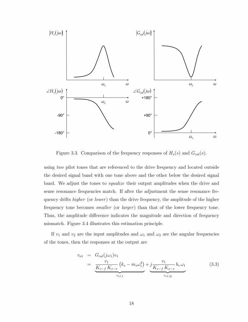
location of the complex zeros. Figure 3.3 compares the frequency responses of Hs(s)
and Gcal(s). The notch and 90 phase lead of Gcal(s) exactly mirror the peak and
90 phase lag of Hs(s) at resonance making Gcal(s) an excellent, albeit inverse, proxy
for Hs(s). In a sense, Gcal(s) is preferable over Hs(s) because it avoids the high-Q
poles in Hs(s) that severely limit the tracking bandwidth of conventional open-loop
sensing based frequency calibration techniques [9].
One possible way to use the calibration input to estimate the frequency mismatch
is to monitor the phase shift from the calibration input to the output using a pilot
tone at the drive frequency. Unfortunately, this approach is problematic because the
tone would invariably interfere with the Coriolis signal. We overcome this problem by
17
0°
-90°
-180°
( )jωHs
( )jωHs∠
ω
ω
sω
sω+180°
+90°
0°
( )jωGcal
( )jωGcal∠
ω
ω
sω
sω
Figure 3.3. Comparison of the frequency responses of Hs(s) and Gcal(s).
using two pilot tones that are referenced to the drive frequency and located outside
the desired signal band with one tone above and the other below the desired signal
band. We adjust the tones to equalize their output amplitudes when the drive and
sense resonance frequencies match. If after the adjustment the sense resonance fre-
quency drifts higher (or lower) than the drive frequency, the amplitude of the higher
frequency tone becomes smaller (or larger) than that of the lower frequency tone.
Thus, the amplitude difference indicates the magnitude and direction of frequency
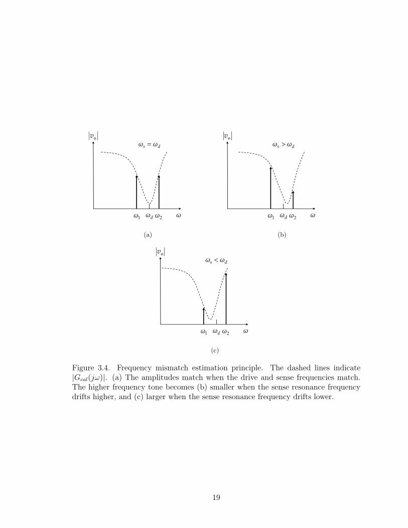
mismatch. Figure 3.4 illustrates this estimation principle.
If v1 and v2 are the input amplitudes and ω1 and ω2 are the angular frequencies
of the tones, then the responses at the output are
vo1 = Gcal(jω1)v1
=v1
Kv−f Kx−v
(ks −msω
21
)︸ ︷︷ ︸
vo1,I
+ jv1
Kv−f Kx−vbs ω1︸ ︷︷ ︸
vo1,Q
(3.3)
18
dω ω
1ω
2ω
dsωω =
ov
(a)
dω ω
1ω
2ω
dsωω >
ov
(b)
ov
dω ω
1ω
2ω
dsωω <
(c)
Figure 3.4. Frequency mismatch estimation principle. The dashed lines indicate|Gcal(jω)|. (a) The amplitudes match when the drive and sense frequencies match.The higher frequency tone becomes (b) smaller when the sense resonance frequencydrifts higher, and (c) larger when the sense resonance frequency drifts lower.
19
Coriolis
Force
Position
To Voltage
Sense
Dynamics
Compensator
vxK −( )sHs ( )sHc
Voltage
To Force
fvK −
( ) ( )4444 34444 21tωvtωv2211
coscos +
errv
sk ( ) ( )444 3444 21tt21
coscos ωω +
errveKsk
s,optk
Estimator
Gain
Figure 3.5. Estimator realization and linearized model.
and
vo2 = Gcal(jω2)v2
=v2
Kv−f Kx−v
(ks −msω
22
)︸ ︷︷ ︸
vo2,I
+ jv2
Kv−f Kx−vbs ω2︸ ︷︷ ︸
vo2,Q
. (3.4)
The in-phase terms vo1,I and vo2,I are useful since they are modulated by ks. The
quadrature terms vo1,Q and vo2,Q are useless and are rejected by synchronously de-
modulating the in-phase terms. Their rejection makes this approach insensitive to
damping factor variations to first order. Another welcome feature of synchronous
demodulation is that it preserves the signs of the in-phase terms. This, combined
with the phase inversion beyond the sense resonance frequency, allows amplitude
differencing to be realized by simply summing vo1,I and vo2,I.
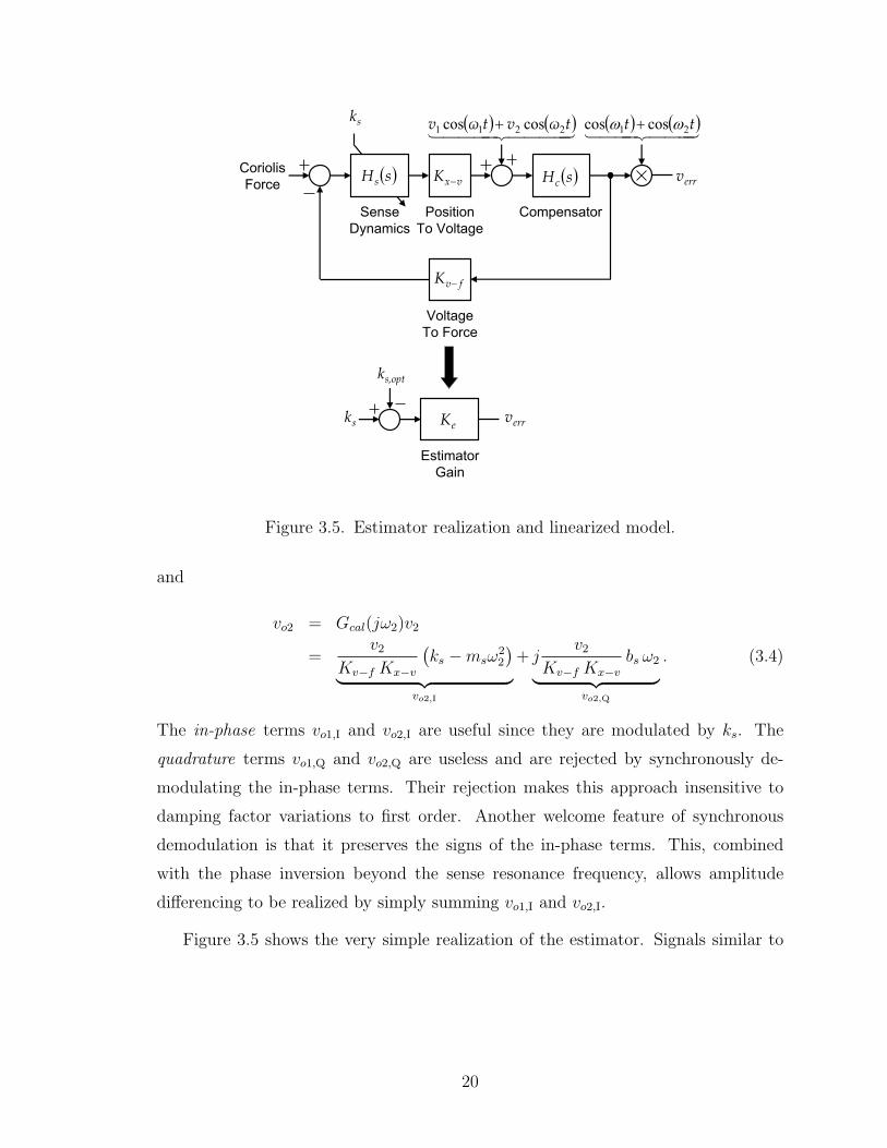
Figure 3.5 shows the very simple realization of the estimator. Signals similar to
20
the pilot tones are used in the demodulation. The final error signal is
verr = vo1,I + vo2,I
=v1 + v2
Kv−f Kx−v︸ ︷︷ ︸estimator gain
ks −ms
ω21
1 +v2
v1
+ω2
2
1 +v1
v2
︸ ︷︷ ︸
reference stiffness
. (3.5)
We adjust the pilot tone parameters as previously mentioned such that the reference
stiffness is equal to the optimal stiffness ks,opt. If we fix the tone frequencies to
ω1 = ωd − ωcal and ω2 = ωd + ωcal, then the amplitudes must satisfy
v2
v1
=2ωd − ωcal2ωd + ωcal
. (3.6)
The unequal amplitudes account for the logarithmic nature of frequency behavior
and the asymmetry between the low and high frequency responses of Gcal(s). The
constraint results in an error signal that is exactly proportional to the difference
between the actual stiffness and the optimal stiffness, i.e. verr = Ke (ks − ks,opt)where Ke is the estimator gain.
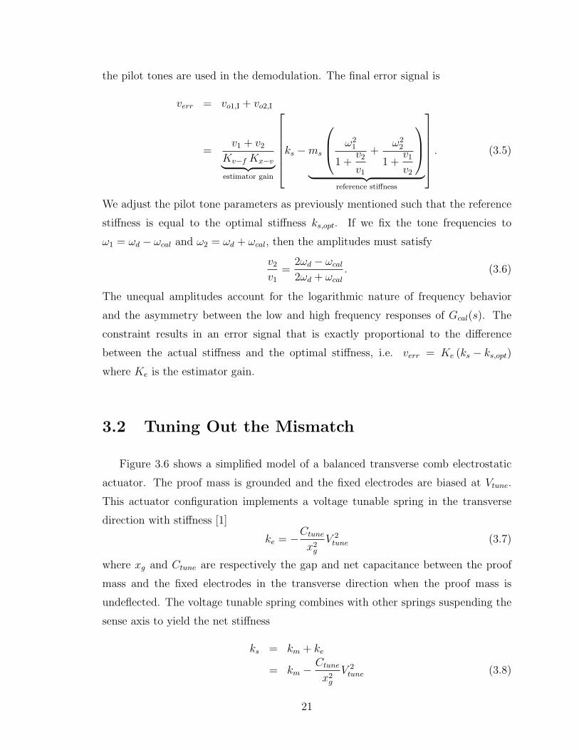
3.2 Tuning Out the Mismatch
Figure 3.6 shows a simplified model of a balanced transverse comb electrostatic
actuator. The proof mass is grounded and the fixed electrodes are biased at Vtune.
This actuator configuration implements a voltage tunable spring in the transverse
direction with stiffness [1]
ke = −Ctunex2g
V 2tune (3.7)
where xg and Ctune are respectively the gap and net capacitance between the proof
mass and the fixed electrodes in the transverse direction when the proof mass is
undeflected. The voltage tunable spring combines with other springs suspending the
sense axis to yield the net stiffness
ks = km + ke
= km −Ctunex2g
V 2tune (3.8)
21
tuneV
sx
Figure 3.6. Voltage tunable spring implemented by a balanced transverse comb elec-trostatic actuator.
where km is the combined stiffness of the other springs consisting mainly of flex-
tures and parasitic springs from electrostatic force feedback and quadrature nulling.
Since the tunable spring only softens ks, it is important to design the flextures to be
stiffer than the optimal stiffness by sufficient margin to accommodate force feedback
and quadrature nulling induced spring softening in addition to process and ambient
variations.
The position sense electrodes are normally realized by transverse combs and thus
can double as tuning combs, eliminating the need for a set of electrodes dedicated
to stiffness tuning only. Time multiplexing position sensing and stiffness tuning at
a sufficiently high rate is one way to share the electrodes. In this case, the effective
electrostatic stiffness is scaled by the duty factor of the stiffness tuning phase. From
the point of view of minimizing power dissipation, however, a dedicated set of tuning
combs is preferable to avoid the typically substantial power penalty associated with
charging and discharging the sense capacitors at a high rate.
3.3 Closing the Tuning Loop
The frequency mismatch estimator and voltage tunable spring comprise the nec-
essary elements to implement automatic resonance frequency tuning. The only re-
maining element is a controller to close the tuning loop. The controller should drive
the frequency mismatch estimate to zero and remain stable at all operating points.
22
errv
eKsk
s,optk
( )sH f
Estimator
Gain
Loop
Filter
Tunable
Spring
( )2*tune2
tune Vx
C
g
−
Inverse
Nonlinearity
( )tunerefVVsqrt
*tuneV
tuneVmk
ek
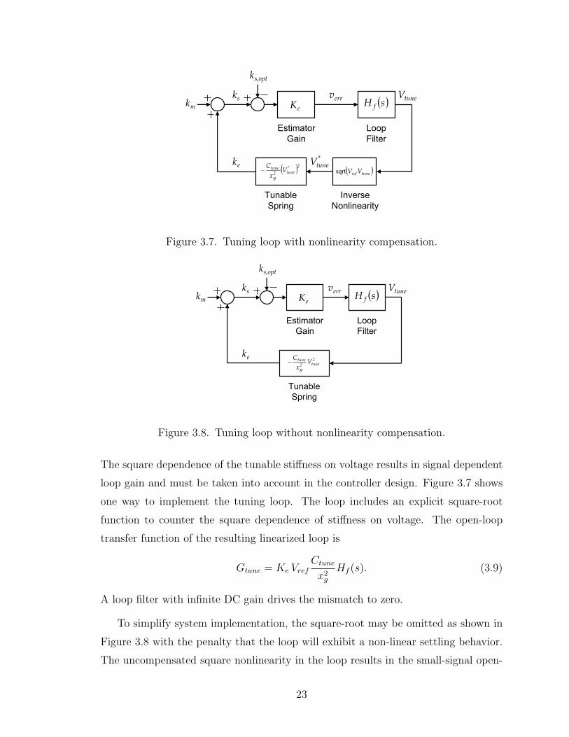
Figure 3.7. Tuning loop with nonlinearity compensation.
errv
eK ( )sH f
Estimator
Gain
Loop
Filter
Tunable
Spring
2
tune2tune Vx
C
g
−
tuneV
s,optk
mksk
ek
Figure 3.8. Tuning loop without nonlinearity compensation.
The square dependence of the tunable stiffness on voltage results in signal dependent
loop gain and must be taken into account in the controller design. Figure 3.7 shows
one way to implement the tuning loop. The loop includes an explicit square-root
function to counter the square dependence of stiffness on voltage. The open-loop
transfer function of the resulting linearized loop is
Gtune = Ke VrefCtunex2g
Hf (s). (3.9)
A loop filter with infinite DC gain drives the mismatch to zero.
To simplify system implementation, the square-root may be omitted as shown in
Figure 3.8 with the penalty that the loop will exhibit a non-linear settling behavior.
The uncompensated square nonlinearity in the loop results in the small-signal open-
23
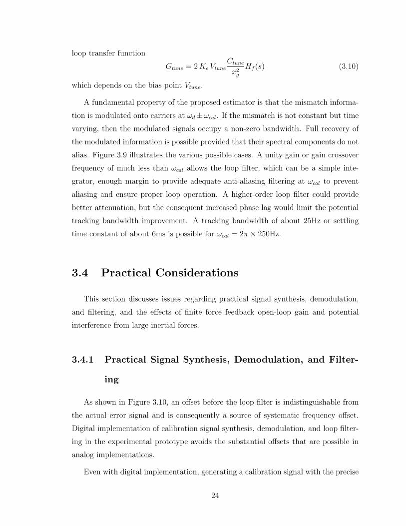
loop transfer function
Gtune = 2Ke VtuneCtunex2g
Hf (s) (3.10)
which depends on the bias point Vtune.
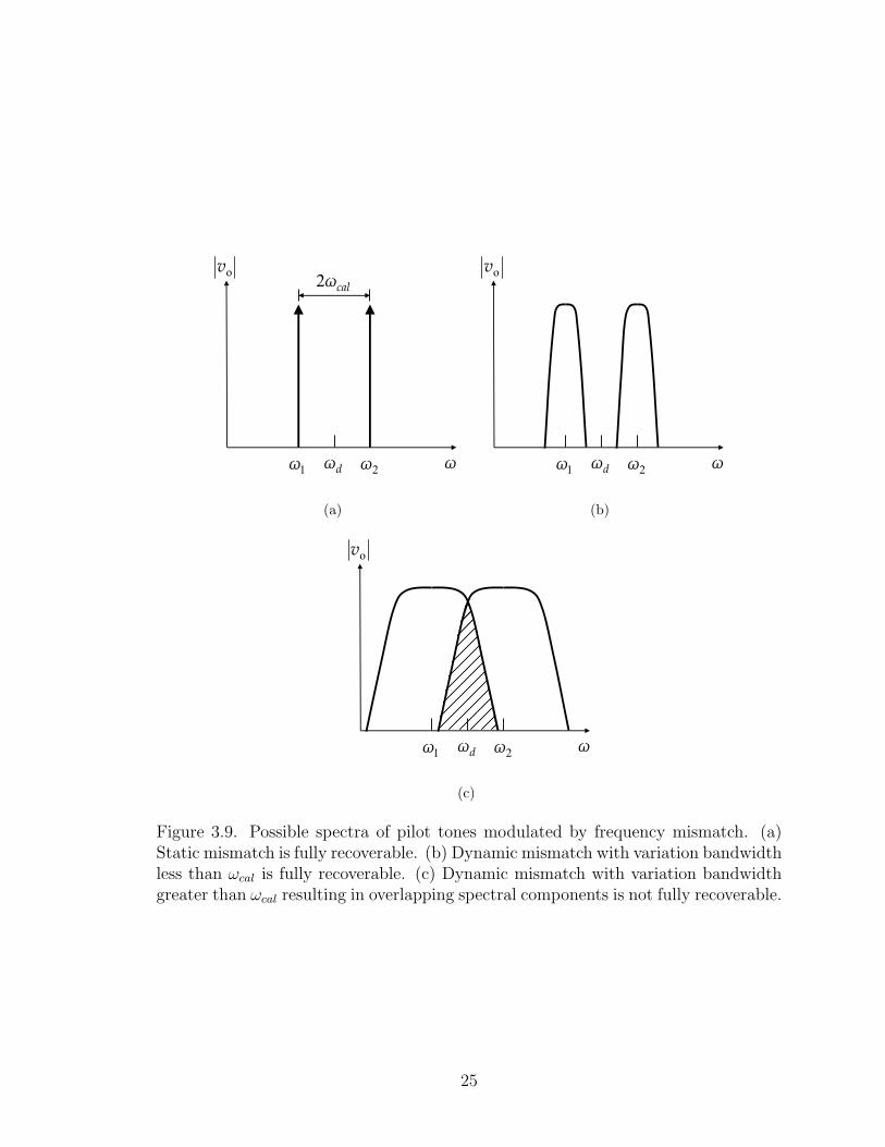
A fundamental property of the proposed estimator is that the mismatch informa-
tion is modulated onto carriers at ωd±ωcal. If the mismatch is not constant but time
varying, then the modulated signals occupy a non-zero bandwidth. Full recovery of
the modulated information is possible provided that their spectral components do not
alias. Figure 3.9 illustrates the various possible cases. A unity gain or gain crossover
frequency of much less than ωcal allows the loop filter, which can be a simple inte-
grator, enough margin to provide adequate anti-aliasing filtering at ωcal to prevent
aliasing and ensure proper loop operation. A higher-order loop filter could provide
better attenuation, but the consequent increased phase lag would limit the potential
tracking bandwidth improvement. A tracking bandwidth of about 25Hz or settling
time constant of about 6ms is possible for ωcal = 2π × 250Hz.
3.4 Practical Considerations
This section discusses issues regarding practical signal synthesis, demodulation,
and filtering, and the effects of finite force feedback open-loop gain and potential
interference from large inertial forces.
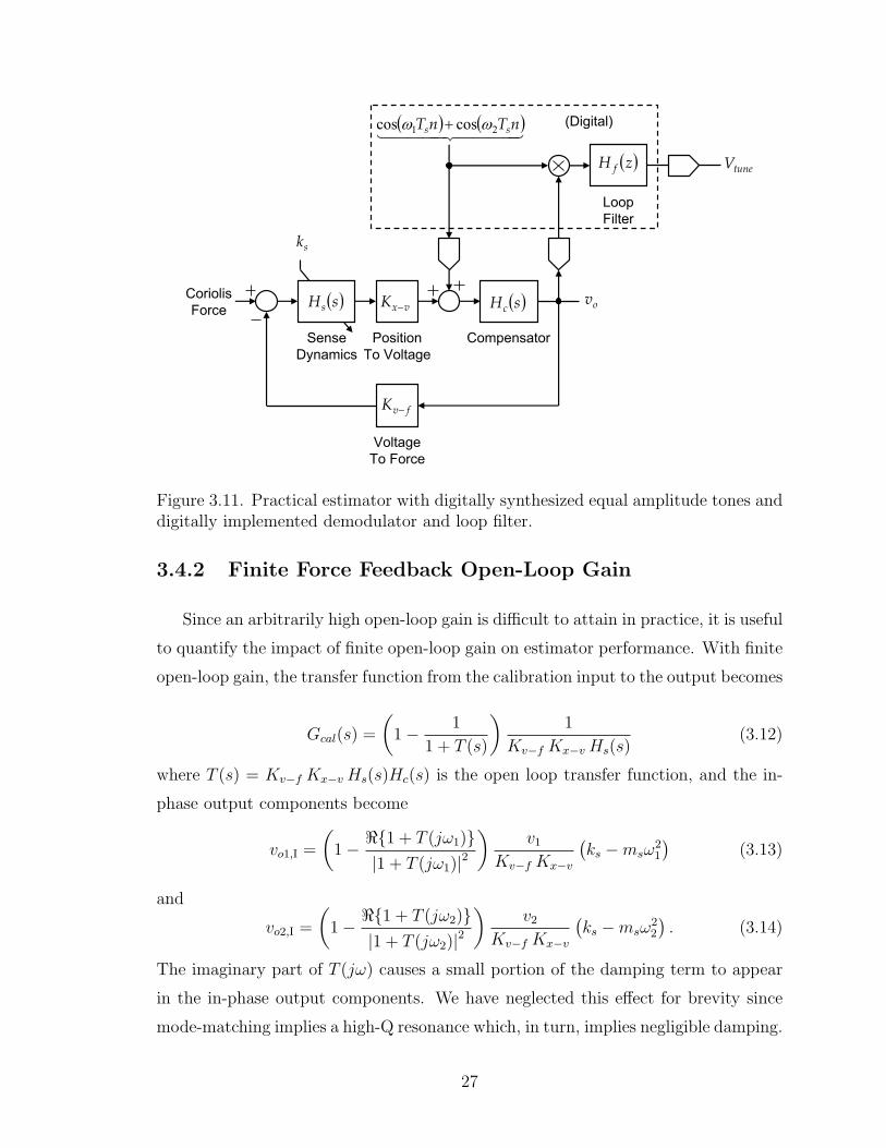
3.4.1 Practical Signal Synthesis, Demodulation, and Filter-
ing
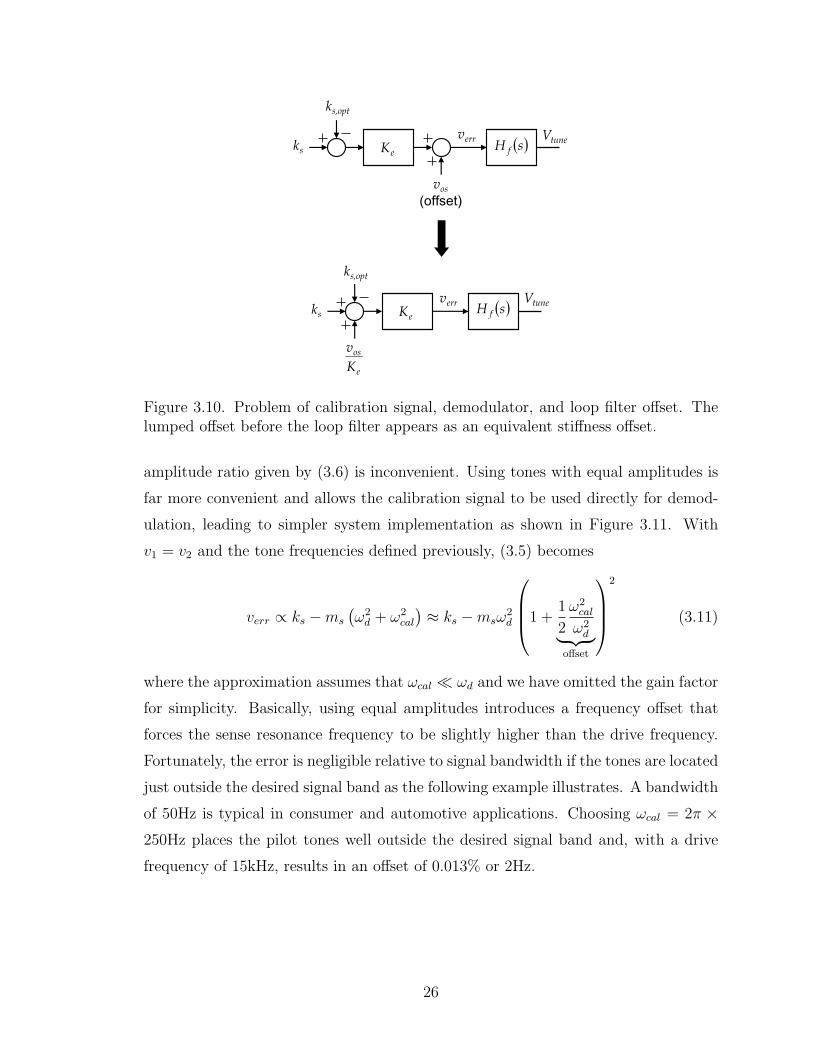
As shown in Figure 3.10, an offset before the loop filter is indistinguishable from
the actual error signal and is consequently a source of systematic frequency offset.
Digital implementation of calibration signal synthesis, demodulation, and loop filter-
ing in the experimental prototype avoids the substantial offsets that are possible in
analog implementations.
Even with digital implementation, generating a calibration signal with the precise
24
dω
ov
ω1ω
2ω
calω2
(a)
ov
dω ω
1ω
2ω
(b)
ov
dω ω
1ω
2ω
(c)
Figure 3.9. Possible spectra of pilot tones modulated by frequency mismatch. (a)Static mismatch is fully recoverable. (b) Dynamic mismatch with variation bandwidthless than ωcal is fully recoverable. (c) Dynamic mismatch with variation bandwidthgreater than ωcal resulting in overlapping spectral components is not fully recoverable.
25
eKsk
s,optk
( )sH ftuneV
e
os
K
v
eKsk
s,optk
( )sH f
(offset)
tuneV
osv
errv
errv
Figure 3.10. Problem of calibration signal, demodulator, and loop filter offset. Thelumped offset before the loop filter appears as an equivalent stiffness offset.
amplitude ratio given by (3.6) is inconvenient. Using tones with equal amplitudes is
far more convenient and allows the calibration signal to be used directly for demod-
ulation, leading to simpler system implementation as shown in Figure 3.11. With
v1 = v2 and the tone frequencies defined previously, (3.5) becomes
verr ∝ ks −ms
(ω2d + ω2
cal
)≈ ks −msω
2d
1 +1
2
ω2cal
ω2d︸ ︷︷ ︸
offset
2
(3.11)
where the approximation assumes that ωcal ωd and we have omitted the gain factor
for simplicity. Basically, using equal amplitudes introduces a frequency offset that
forces the sense resonance frequency to be slightly higher than the drive frequency.
Fortunately, the error is negligible relative to signal bandwidth if the tones are located
just outside the desired signal band as the following example illustrates. A bandwidth
of 50Hz is typical in consumer and automotive applications. Choosing ωcal = 2π ×250Hz places the pilot tones well outside the desired signal band and, with a drive
frequency of 15kHz, results in an offset of 0.013% or 2Hz.
26
Coriolis
Force
Position
To Voltage
Compensator
vxK −( )sHs ( )sHc
fvK −
sk
( ) ( )4444 34444 21nTnT ss 21
coscos ωω +
ov
(Digital)
( )zH f
Loop
Filter
tuneV
Sense
Dynamics
Voltage
To Force
Figure 3.11. Practical estimator with digitally synthesized equal amplitude tones anddigitally implemented demodulator and loop filter.
3.4.2 Finite Force Feedback Open-Loop Gain
Since an arbitrarily high open-loop gain is difficult to attain in practice, it is useful
to quantify the impact of finite open-loop gain on estimator performance. With finite
open-loop gain, the transfer function from the calibration input to the output becomes
Gcal(s) =
(1− 1
1 + T (s)
)1
Kv−f Kx−vHs(s)(3.12)
where T (s) = Kv−f Kx−vHs(s)Hc(s) is the open loop transfer function, and the in-
phase output components become
vo1,I =
(1− <1 + T (jω1)
|1 + T (jω1)|2
)v1
Kv−f Kx−v
(ks −msω
21
)(3.13)
and
vo2,I =
(1− <1 + T (jω2)
|1 + T (jω2)|2
)v2
Kv−f Kx−v
(ks −msω
22
). (3.14)
The imaginary part of T (jω) causes a small portion of the damping term to appear
in the in-phase output components. We have neglected this effect for brevity since
mode-matching implies a high-Q resonance which, in turn, implies negligible damping.
27
It is evident from the above equations that finite open-loop gain introduces errors
in the tone amplitudes. Only a negligible estimator gain error arises if the amplitude
errors in vo1,I and vo2,I match, otherwise a frequency offset also arises. Assuming a
minimum open-loop gain of Tmin, the worst case mismatch occurs when T (jω1) = Tmin
and T (jω2) = −Tmin or vice versa. In this case, the error signal is
verr ∝ ks −ms
(ω2d +
2
Tminωdωcal
)≈ ks −msω
2d
1 +1
Tmin
ωcalωd︸ ︷︷ ︸
offset
2
. (3.15)
Fortunately, the offset is negligible for any reasonable open-loop gain. Continuing
with the previous example where ωcal = 2π × 250Hz, a minimum open-loop gain of
40dB results in a worst case offset of 0.017% or 2.5Hz.
3.4.3 Interference from Large Inertial Forces
Since there is no filter to limit the bandwidth of Coriolis and other inertial forces
that appear on the sense axis, spectral components of those forces around ωd ± ωcalcan interfere with the pilot tones and produce signal dependent frequency offset. The
use of a tuning fork structure largely rejects the linear acceleration component leaving
the Coriolis acceleration component. In the following analysis, we quantify the worst
case error that the Coriolis acceleration component can contribute.
The Coriolis acceleration can be expressed as
ac = 2 Ω xd + Ωxd. (3.16)
The Ωxd term captures an often neglected higher order effect that is important in
the following analysis. The worst case interference occurs when the angular rate is
sinusoidally varying at ωcal in which case the angular rate can be expressed as
Ω = Ω0 cos(ωcalt+ φΩ). (3.17)
where Ω0 is the amplitude and φΩ is the phase which can assume any value. If the
drive axis oscillates according to xd = xd0 cos(ωdt), then the Coriolis acceleration
28
resulting from the angular rate is
ac = − 2 Ω0 ωd xd0 cos(ωcalt+ φΩ) sin(ωdt)︸ ︷︷ ︸2 Ω xd
−Ω0 ωcal xd0 sin(ωcalt+ φΩ) cos(ωdt)︸ ︷︷ ︸Ωxd
.
(3.18)
The acceleration appears at the output of the force feedback loop scaled by ms/Kv−f
(see Figure 3.2). The 2 Ω xd term dominates by far since it is multiplied by ωd while the
Ωxd term is multiplied by the much smaller ωcal. It is therefore important to generate
the calibration and demodulation signals by using a sinusoid at ωcal to modulate the
amplitude of a carrier that is in phase with the drive displacement (and thus in
quadrature with the drive velocity) to enable the rejection of the dominant 2 Ω xd
term. After demodulation, the Ωxd term remains and the error signal becomes
verr = Ke
(ks −msω
2d
)− ms
Kv−fΩ0 ωcal xd0︸ ︷︷ ︸
worst case
. (3.19)
The consequent offset error is minimized by maximizing the estimator gain Ke which
requires the use of large amplitude pilot tones. The amplitudes can not be arbi-
trarily large, however, since the resulting output signals must live within the force
feedback loop’s limited output range. As we have already seen in Figure 3.4, the out-
put amplitudes of the tones vary substantially with frequency mismatch. Since the
amplitudes at worst case frequency mismatch can be substantially higher than with
perfect matching, the amplitudes should be small enough to avoid overloading the
output during startup when the system has the worst case frequency mismatch. As
frequency matching improves, the amplitudes, and consequently the estimator gain,
may be increased to minimize the impact of Coriolis interference. It is important to
reciprocally lower some other gain factor while increasing estimator gain to maintain
an optimal tracking bandwidth. If the pilot tones are maximized, then for full-scale
Coriolis acceleration sinusoidally varying at the worst frequency and with the worst
phase, the resulting fractional matching error is on the order of ω2cal/ω
2d, which is
similar to the magnitude of the other errors.
29
3.5 Summary
This chapter introduces a technique for detecting and tuning out the mismatch
between the drive and sense resonance frequencies of a force balanced gyroscope. The
technique estimates the frequency mismatch by injecting out-of-band pilot tones into
an appropriate point in the force feedback. Electrostatic spring softening using a
balanced transverse comb electrostatic actuator enables the fine tuning of the sense
resonance. A loop filter with infinite DC gain drives the mismatch to zero. Digital
synthesis of the calibration signal and implementation of the demodulator and loop
filter prevents the presence of a large systematic frequency offset. Yet to be presented
is the design of the force feedback loop, the crucial element upon which the proposed
mode-matching technique depends. The next chapter begins consideration of the
design of the force feedback loop with particular focus on the position sense front-
end.
30
Chapter 4
Position Sensing
As discussed in Chapter 2, the position sense front-end sets the electronic noise
floor and dominates the power dissipation of the readout interface, and as further
discussed, mode-matching is the most effective way to improve the power efficiency of
the overall readout interface. Another yet to be explored, but potentially rewarding
way is to directly improve the power efficiency of the dominant power dissipator, the
position sense front-end. Since feedback in general relaxes certain accuracy require-
ments of the blocks in the forward path, force feedback presents a special opportunity
to trade the well defined and highly linear gain of state-of-the-art front-ends for much
lower noise given the same bias current. This chapter focuses on the subject of directly
improving the power efficiency of the front-end.
4.1 Force Feedback Loop Stability Consideration
As argued in a previous chapter, force feedback enables effective exploitation of the
sense resonance. Unfortunately, with feedback comes the problem of possible closed-
loop instability. Previous work has shown that stability at atmospheric pressure is no
guarantee of stability in vacuum [10, 11]. The problem is caused by the so far neglected
but usually present higher-order resonance modes of the mechanical structure arising
from resonances of the suspension or electrostatic drive and sense comb fingers for
31
example. While normally over-damped at atmospheric pressure, these modes are
highly under-damped in vacuum where they destabilize loops employing traditional
lead compensation [12].
The force feedback loop is said to employ collocated control if position sensing
and force feedback share the same set of electrodes. Conversely, it is said to employ
non-collocated control if they each use dedicated electrodes. In the latter case, the
dynamics between the position sensing and force feedback electrostatic comb fingers
introduce additional unwelcome phase lag into the response of the mechanical struc-
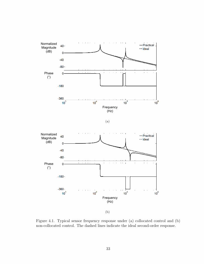
ture [13]. Figure 4.1 illustrates the frequency responses that are possible under both
configurations with a higher-order resonance at 100kHz. The flipping of the order-
ing of the resonance and anti-resonance, possible only in the case of non-collocated
control, results in the phase lag approaching 360 near the second resonance peak.
Collocated control is preferable since it guarantees the presence of a phase restoring
anti-resonance between any pair of successive resonances. The anti-resonance pre-
vents the phase lag from exceeding 180 near resonance peaks and thereby facilitates
force feedback loop compensation.
While frequency-multiplexing position sensing and force feedback onto the same
set of electrodes realizes collocated control [8], the inherently continuous-time tech-
nique requires the use of proportional feedback which complicates the task of mode-
matching as will be explained in the next chapter. Bang-bang feedback avoids the
complication but is only possible if time-multiplexing is used. The discontinuous-time
operation inherent in time-multiplexing implies the use of a sampling front-end.
4.2 Sampling and Noise Folding
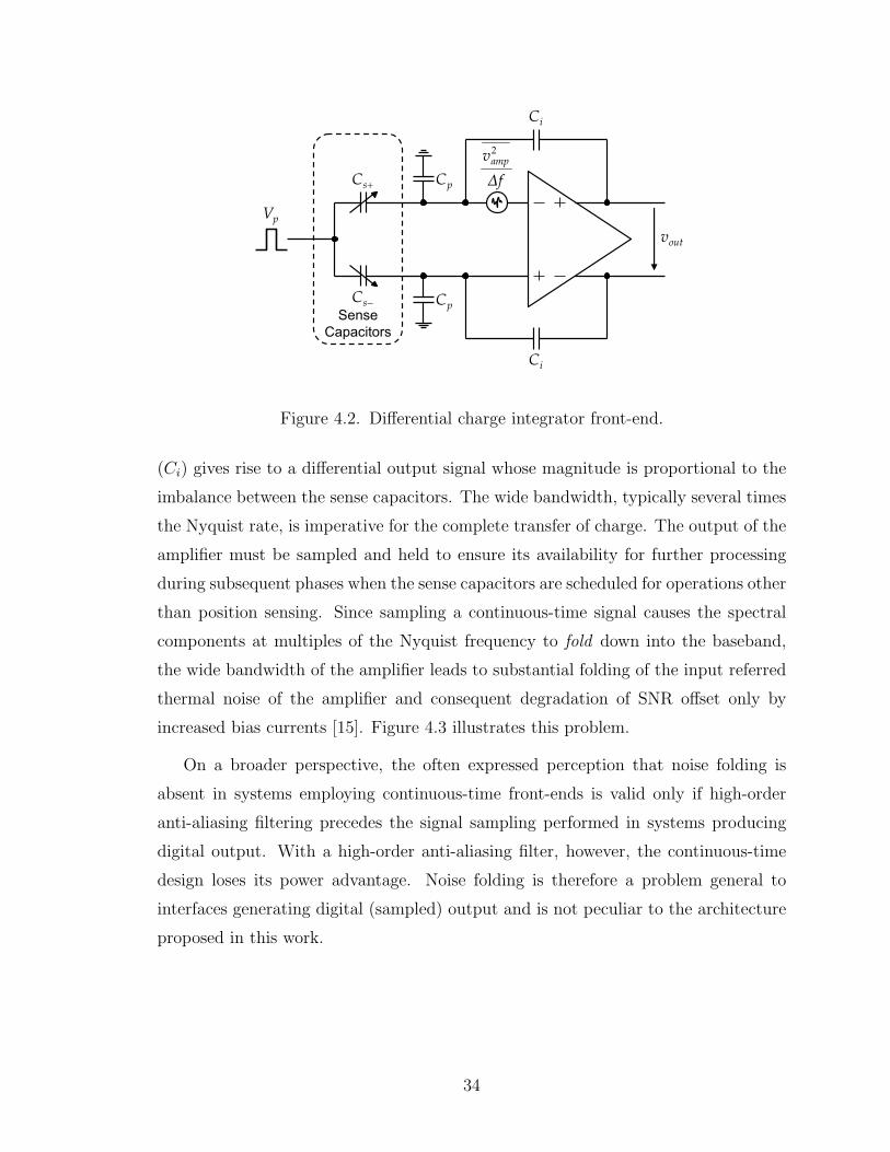
Figure 4.2 shows the traditional front-end used to convert an imbalance between
the sense capacitors to voltage [14]. Based on charge integration, the front-end uses
a wideband capacitive feedback amplifier to provide a highly accurate gain that is
insensitive to ambient variations. During the position sensing phase of the time-
multiplexing operation, a voltage pulse is applied on the proof mass node. The
resulting transfer of charge from the sense capacitors to the integration capacitors
32
Frequency
(Hz)
Normalized
Magnitude
(dB)
Phase
(°)
Frequency
(Hz)
Normalized
Magnitude
(dB)
Phase
(°)
(a)
Frequency
(Hz)
Normalized
Magnitude
(dB)
Phase
(°)
Frequency
(Hz)
Normalized
Magnitude
(dB)
Phase
(°)
(b)
Figure 4.1. Typical sensor frequency response under (a) collocated control and (b)non-collocated control. The dashed lines indicate the ideal second-order response.
33
−sC
+sC
pC
pC
outv
∆f
vamp2
iC
iC
Sense
Capacitors
pV
Figure 4.2. Differential charge integrator front-end.
(Ci) gives rise to a differential output signal whose magnitude is proportional to the
imbalance between the sense capacitors. The wide bandwidth, typically several times
the Nyquist rate, is imperative for the complete transfer of charge. The output of the
amplifier must be sampled and held to ensure its availability for further processing
during subsequent phases when the sense capacitors are scheduled for operations other
than position sensing. Since sampling a continuous-time signal causes the spectral
components at multiples of the Nyquist frequency to fold down into the baseband,
the wide bandwidth of the amplifier leads to substantial folding of the input referred
thermal noise of the amplifier and consequent degradation of SNR offset only by
increased bias currents [15]. Figure 4.3 illustrates this problem.
On a broader perspective, the often expressed perception that noise folding is
absent in systems employing continuous-time front-ends is valid only if high-order
anti-aliasing filtering precedes the signal sampling performed in systems producing
digital output. With a high-order anti-aliasing filter, however, the continuous-time
design loses its power advantage. Noise folding is therefore a problem general to
interfaces generating digital (sampled) output and is not peculiar to the architecture
proposed in this work.
34
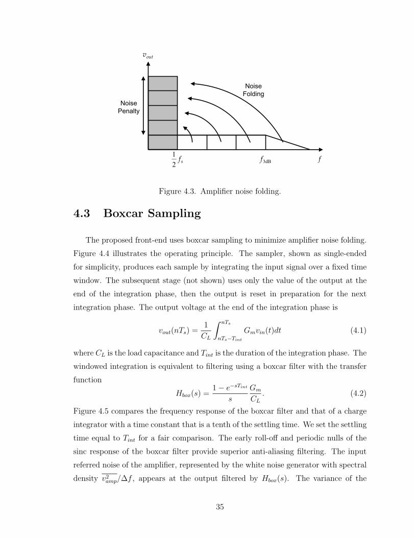
fsf2
1dB3f
Noise
Penalty
Noise
Folding
outv
Figure 4.3. Amplifier noise folding.
4.3 Boxcar Sampling
The proposed front-end uses boxcar sampling to minimize amplifier noise folding.
Figure 4.4 illustrates the operating principle. The sampler, shown as single-ended
for simplicity, produces each sample by integrating the input signal over a fixed time
window. The subsequent stage (not shown) uses only the value of the output at the
end of the integration phase, then the output is reset in preparation for the next
integration phase. The output voltage at the end of the integration phase is
vout(nTs) =1
CL
∫ nTs
nTs−Tint
Gmvin(t)dt (4.1)
where CL is the load capacitance and Tint is the duration of the integration phase. The
windowed integration is equivalent to filtering using a boxcar filter with the transfer
function
Hbox(s) =1− e−sTint
s
Gm
CL. (4.2)
Figure 4.5 compares the frequency response of the boxcar filter and that of a charge
integrator with a time constant that is a tenth of the settling time. We set the settling
time equal to Tint for a fair comparison. The early roll-off and periodic nulls of the
sinc response of the boxcar filter provide superior anti-aliasing filtering. The input
referred noise of the amplifier, represented by the white noise generator with spectral
density v2amp/∆f , appears at the output filtered by Hbox(s). The variance of the
35
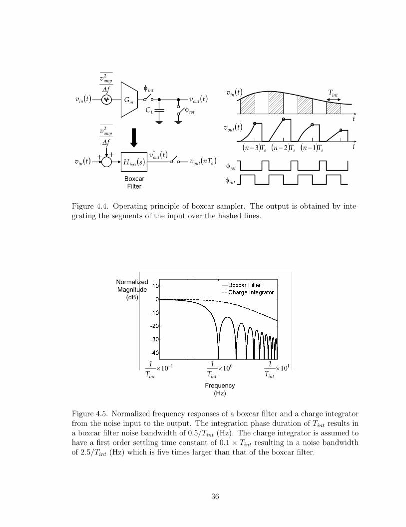
mG
rstφ
intφ
( )tvin
LC
( )tvout
rstφ
intφ
( )tvin
( )tvout
intT
t
t( ) sTn 1−( ) sTn 2−( ) sTn 3−
( )sHbox
Boxcar
Filter
( )tv*out( )tvin ( )sout nTv
∆f
vamp2
∆f
vamp2
Figure 4.4. Operating principle of boxcar sampler. The output is obtained by inte-grating the segments of the input over the hashed lines.
110
−×
intT
1 010×
intT
1 110×
intT
1
Frequency
(Hz)
Normalized
Magnitude
(dB)
110
−×
intT
1 010×
intT
1 110×
intT
1
Frequency
(Hz)
Normalized
Magnitude
(dB)
Figure 4.5. Normalized frequency responses of a boxcar filter and a charge integratorfrom the noise input to the output. The integration phase duration of Tint results ina boxcar filter noise bandwidth of 0.5/Tint (Hz). The charge integrator is assumed tohave a first order settling time constant of 0.1 × Tint resulting in a noise bandwidthof 2.5/Tint (Hz) which is five times larger than that of the boxcar filter.
36
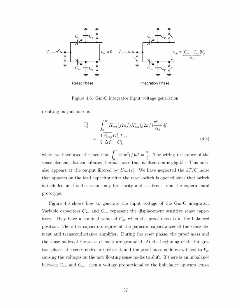
−sC
pV
+sC
0=inv
pC
pC
( ) p
∆C
ssin VCCv
s
43421 −+ −∝
Reset Phase
−sC
pV
+sC
pC
pC
Integration Phase
Figure 4.6. Gm-C integrator input voltage generation.
resulting output noise is
v2n =
∫ ∞0
Hbox(j2πf)H∗box(j2πf)v2amp
∆fdf
=1
2
v2amp
∆f
G2mTintC2L
(4.3)
where we have used the fact that
∫ ∞0
sinc2(f)df =π
2. The wiring resistance of the
sense element also contributes thermal noise that is often non-negligible. This noise
also appears at the output filtered by Hbox(s). We have neglected the kT/C noise
that appears on the load capacitor after the reset switch is opened since that switch
is included in this discussion only for clarity and is absent from the experimental
prototype.
Figure 4.6 shows how to generate the input voltage of the Gm-C integrator.
Variable capacitors Cs+ and Cs− represent the displacement sensitive sense capac-
itors. They have a nominal value of Cs0 when the proof mass is in the balanced
position. The other capacitors represent the parasitic capacitances of the sense ele-
ment and transconductance amplifier. During the reset phase, the proof mass and
the sense nodes of the sense element are grounded. At the beginning of the integra-
tion phase, the sense nodes are released, and the proof mass node is switched to Vp,
causing the voltages on the now floating sense nodes to shift. If there is an imbalance
between Cs+ and Cs−, then a voltage proportional to the imbalance appears across
37
the sense nodes with the value
vin = (Vp − Vcm)∆Cs
Cs0 + Cp
=
1− Cs0Cs0 + Cp︸ ︷︷ ︸gain error
∆CsCs0 + Cp
Vp (4.4)
where ∆Cs = Cs+ − Cs−. The shift in the common mode voltage of the sense nodes
reduces the effective voltage across the sense capacitors, causing a gain error that
can be minimized using common-mode feedback (CMFB). In our implementation, we
forgo CMFB to avoid the additional power dissipation and loading of the sense nodes
by the CMFB circuit since in the experimental prototype, the parasitic capacitance
dominates over the sense capacitance, resulting in only a modest common-mode shift.
The voltage given by (4.4) is subsequently boxcar sampled. Since the imbalance
between Cs+ and Cs− is essentially static within the relatively short integration inter-
val, the time integration performed by the boxcar sampler reduces to multiplication
by the integration time, and thus
vout =GmTintCL
vi
=GmTintCL
(1− Cs0
Cs0 + Cp
)∆Cs
Cs0 + CpVp. (4.5)
Comparing the SNR of the boxcar sampler and switch-capacitor charge integrator
for the same bias current helps quantify the relative merits of the two techniques.
In the charge integrator (see Figure 4.2), the input referred noise of the amplifier
appears at the output with variance [14]
v2n,sc =
1
4
v2amp
∆f
(Cs0 + Ci + Cp
Ci
)21
τamp. (4.6)
where Ci and τamp are respectively the integration capacitance and settling time
constant of the amplifier, and an imbalance in the sense capacitors results in the
output voltage
vout,sc =
(1− Cs0
Cs0 + Ci + Cp
)∆CsCi
Vp. (4.7)
38
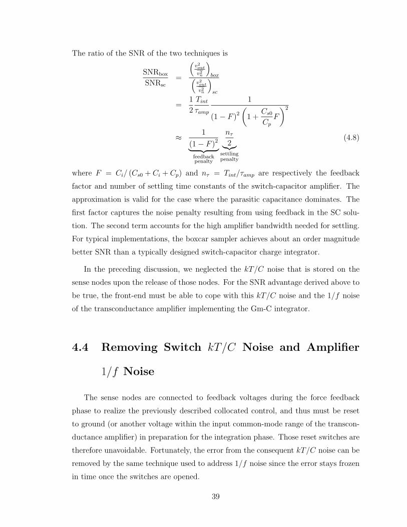
The ratio of the SNR of the two techniques is
SNRbox
SNRsc
=
(v2out
v2n
)box(
v2out
v2n
)sc
=1
2
Tintτamp
1
(1− F )2
(1 +
Cs0Cp
F
)2
≈ 1
(1− F )2︸ ︷︷ ︸feedbackpenalty
nτ2︸︷︷︸
settlingpenalty
(4.8)
where F = Ci/ (Cs0 + Ci + Cp) and nτ = Tint/τamp are respectively the feedback
factor and number of settling time constants of the switch-capacitor amplifier. The
approximation is valid for the case where the parasitic capacitance dominates. The
first factor captures the noise penalty resulting from using feedback in the SC solu-
tion. The second term accounts for the high amplifier bandwidth needed for settling.
For typical implementations, the boxcar sampler achieves about an order magnitude
better SNR than a typically designed switch-capacitor charge integrator.
In the preceding discussion, we neglected the kT/C noise that is stored on the
sense nodes upon the release of those nodes. For the SNR advantage derived above to
be true, the front-end must be able to cope with this kT/C noise and the 1/f noise
of the transconductance amplifier implementing the Gm-C integrator.
4.4 Removing Switch kT/C Noise and Amplifier
1/f Noise
The sense nodes are connected to feedback voltages during the force feedback
phase to realize the previously described collocated control, and thus must be reset
to ground (or another voltage within the input common-mode range of the transcon-
ductance amplifier) in preparation for the integration phase. Those reset switches are
therefore unavoidable. Fortunately, the error from the consequent kT/C noise can be
removed by the same technique used to address 1/f noise since the error stays frozen
in time once the switches are opened.
39
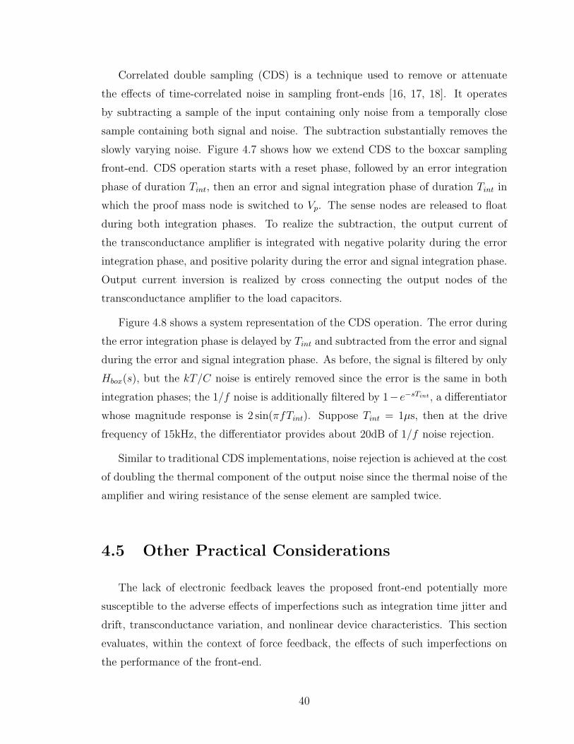
Correlated double sampling (CDS) is a technique used to remove or attenuate
the effects of time-correlated noise in sampling front-ends [16, 17, 18]. It operates
by subtracting a sample of the input containing only noise from a temporally close
sample containing both signal and noise. The subtraction substantially removes the
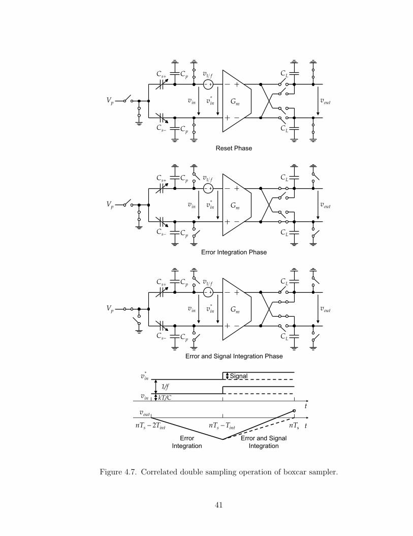
slowly varying noise. Figure 4.7 shows how we extend CDS to the boxcar sampling
front-end. CDS operation starts with a reset phase, followed by an error integration
phase of duration Tint, then an error and signal integration phase of duration Tint in
which the proof mass node is switched to Vp. The sense nodes are released to float
during both integration phases. To realize the subtraction, the output current of
the transconductance amplifier is integrated with negative polarity during the error
integration phase, and positive polarity during the error and signal integration phase.
Output current inversion is realized by cross connecting the output nodes of the
transconductance amplifier to the load capacitors.
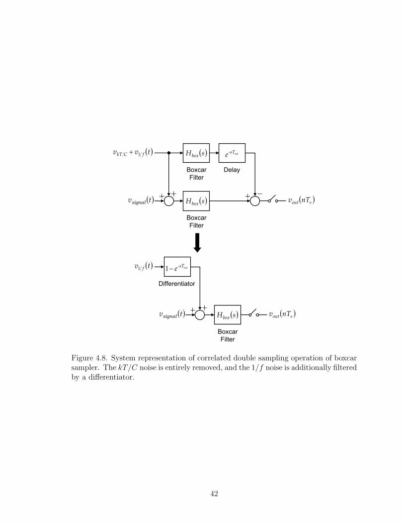
Figure 4.8 shows a system representation of the CDS operation. The error during
the error integration phase is delayed by Tint and subtracted from the error and signal
during the error and signal integration phase. As before, the signal is filtered by only
Hbox(s), but the kT/C noise is entirely removed since the error is the same in both
integration phases; the 1/f noise is additionally filtered by 1−e−sTint , a differentiator
whose magnitude response is 2 sin(πfTint). Suppose Tint = 1µs, then at the drive
frequency of 15kHz, the differentiator provides about 20dB of 1/f noise rejection.
Similar to traditional CDS implementations, noise rejection is achieved at the cost
of doubling the thermal component of the output noise since the thermal noise of the
amplifier and wiring resistance of the sense element are sampled twice.
4.5 Other Practical Considerations
The lack of electronic feedback leaves the proposed front-end potentially more
susceptible to the adverse effects of imperfections such as integration time jitter and
drift, transconductance variation, and nonlinear device characteristics. This section
evaluates, within the context of force feedback, the effects of such imperfections on
the performance of the front-end.
40
−sC
pV
+sC
pC
pC
mG
LC
LC
outv*inv
fv1
inv
Error and Signal Integration Phase
*inv
tsnTints TnT −
Signal
kT/C
1/f
ints TnT 2−
inv
outvt
Error and Signal
Integration
Error
Integration
−sC
pV
+sC
pC
pC
mG
LC
LC
outv
fv1
Error Integration Phase
*invinv
−sC
pV
+sC
pC
pC
Reset Phase
mG
fv1
LC
LC
outv*invinv
Figure 4.7. Correlated double sampling operation of boxcar sampler.
41
( )sHbox
Boxcar
Filter
( )tvsignal ( )sout nTv
( )sHbox
Boxcar
Filter
( )tvv fCkT 1+ int-sTe
Delay
( )sHbox
Boxcar
Filter
( )tvsignal ( )sout nTv
int-sTe−1
Differentiator
( )tv f1
Figure 4.8. System representation of correlated double sampling operation of boxcarsampler. The kT/C noise is entirely removed, and the 1/f noise is additionally filteredby a differentiator.
42
Suppose the integration time is nominally Tint with a small variation ∆Tint, then
vout =GmTintCL
vin
1 +∆TintTint︸ ︷︷ ︸error
. (4.9)
Similar to how force feedback rejects the error due to the sense mode quality factor
drift, force feedback rejects the error resulting from the slow drift of the integration
time. Of concern is the random jitter, which mixes with vin to produce a random
error. To avoid degrading the intrinsic noise floor of the amplifier, the variance of the
error should be well below the RMS noise of the amplifier or
v2in
(∆TintTint
)2
v2amp
∆f
fs2. (4.10)
where fs is the system sampling rate. In the experimental prototype, v2amp/∆f =(
70nV/√
Hz)2
and fs = 480kHz resulting in an RMS noise of 48µV. Thanks to force
feedback, the full-scale vin in the experimental prototype is only on the order of 5mV.
Assuming an RMS jitter of 100ppm, which is very easy to achieve, the variance of the
resulting error is 500nV, two orders of magnitude lower than the intrinsic amplifier
noise.
Transconductance variation, due, for example, to bias current noise and drift, also
gives rise to dynamic gain variation. The nonlinearity of the differential pair used to
realize the transconductance amplifier results in additional signal dependent errors.
As in the case of integration time jitter and drift, the very small input signal level
keeps the resulting errors well within acceptable limits.
4.6 Summary
The traditional position sense front-end suffers from substantial noise folding re-
sulting in the degradation of SNR offset only by increased bias currents. This chapter
proposes boxcar sampling as a way to minimize the noise folding and thereby achieve
significantly higher SNR for the same bias current. Force feedback was proposed in
Chapter 2 as a means to increase the tolerance for process and ambient variations of
the sense element. This chapter extends the idea to the next block in the forward
43
path, the front-end, to enable an order of magnitude improvement in SNR above
and beyond that derived from mode-matching. The next chapter builds upon the
discussion begun in this chapter on force feedback loop design.
44

Chapter 5
Force Feedback
Force feedback is key to effectively exploiting mode-matching and boxcar sampling
for several orders-of-magnitude reduction in overall interface power dissipation. In
the design of the force feedback loop, care must be taken to avoid design choices that
conflict with mode-matching or leave the system susceptible to closed-loop instability.
This chapter focuses on the design of the force feedback loop with particular emphasis
on minimizing analog complexity and power while addressing the above concerns.
5.1 Mode-Matching Consideration
Figure 5.1 shows how to drive the proof mass and position sense electrodes during
the force feedback phase to realize differential actuation. The proof mass is grounded,
and the top and bottom electrodes are biased at Vbias and driven differential by the
feedback voltage vfb. In another approach, the top and bottom electrodes are biased
at Vbias and −Vbias respectively and the proof mass is driven by vfb. Both approaches
produce similar results. However, the first approach is preferable since it requires
only one bias voltage. In any case, the feedback force applied on the proof mass for
45
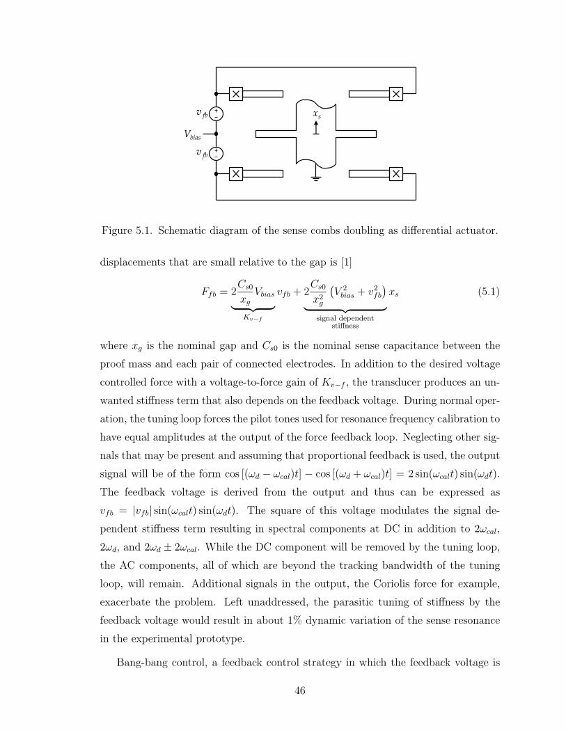
sx
biasV
fbv
fbv
Figure 5.1. Schematic diagram of the sense combs doubling as differential actuator.
displacements that are small relative to the gap is [1]
Ffb = 2Cs0xg
Vbias︸ ︷︷ ︸Kv−f
vfb + 2Cs0x2g
(V 2bias + v2
fb
)︸ ︷︷ ︸
signal dependentstiffness
xs (5.1)
where xg is the nominal gap and Cs0 is the nominal sense capacitance between the
proof mass and each pair of connected electrodes. In addition to the desired voltage
controlled force with a voltage-to-force gain of Kv−f , the transducer produces an un-
wanted stiffness term that also depends on the feedback voltage. During normal oper-
ation, the tuning loop forces the pilot tones used for resonance frequency calibration to
have equal amplitudes at the output of the force feedback loop. Neglecting other sig-
nals that may be present and assuming that proportional feedback is used, the output
signal will be of the form cos [(ωd − ωcal)t] − cos [(ωd + ωcal)t] = 2 sin(ωcalt) sin(ωdt).
The feedback voltage is derived from the output and thus can be expressed as
vfb = |vfb| sin(ωcalt) sin(ωdt). The square of this voltage modulates the signal de-
pendent stiffness term resulting in spectral components at DC in addition to 2ωcal,
2ωd, and 2ωd ± 2ωcal. While the DC component will be removed by the tuning loop,
the AC components, all of which are beyond the tracking bandwidth of the tuning
loop, will remain. Additional signals in the output, the Coriolis force for example,
exacerbate the problem. Left unaddressed, the parasitic tuning of stiffness by the
feedback voltage would result in about 1% dynamic variation of the sense resonance
in the experimental prototype.
Bang-bang control, a feedback control strategy in which the feedback voltage is
46
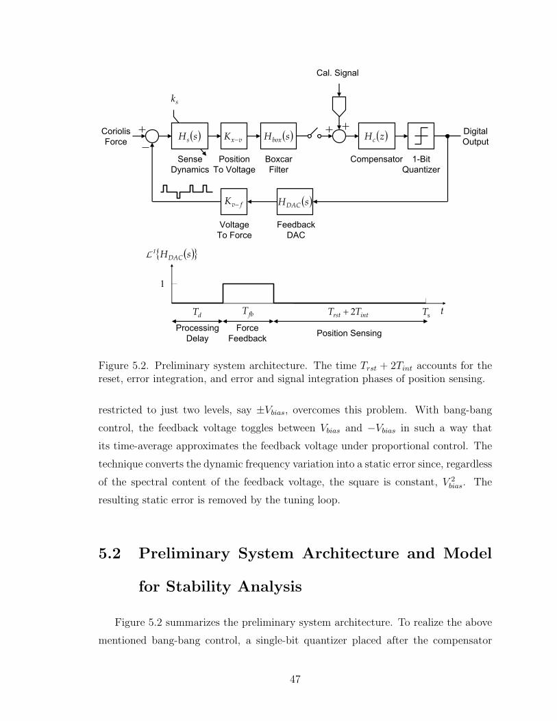
Coriolis
Force
Compensator
vxK −( )sHs ( )zHc
fvK −
sk
Sense
Dynamics
1-Bit
Quantizer
( )sHbox
Boxcar
Filter
Cal. Signal
Voltage
To Force
Digital
Output
Feedback
DAC
( )sHDAC
( ) sHDAC-1L
t
Position SensingForce
Feedback
Processing
Delay
dT fbT sT
1
intrst TT 2+
Position
To Voltage
Figure 5.2. Preliminary system architecture. The time Trst + 2Tint accounts for thereset, error integration, and error and signal integration phases of position sensing.
restricted to just two levels, say ±Vbias, overcomes this problem. With bang-bang
control, the feedback voltage toggles between Vbias and −Vbias in such a way that
its time-average approximates the feedback voltage under proportional control. The
technique converts the dynamic frequency variation into a static error since, regardless
of the spectral content of the feedback voltage, the square is constant, V 2bias. The
resulting static error is removed by the tuning loop.
5.2 Preliminary System Architecture and Model
for Stability Analysis
Figure 5.2 summarizes the preliminary system architecture. To realize the above
mentioned bang-bang control, a single-bit quantizer placed after the compensator
47
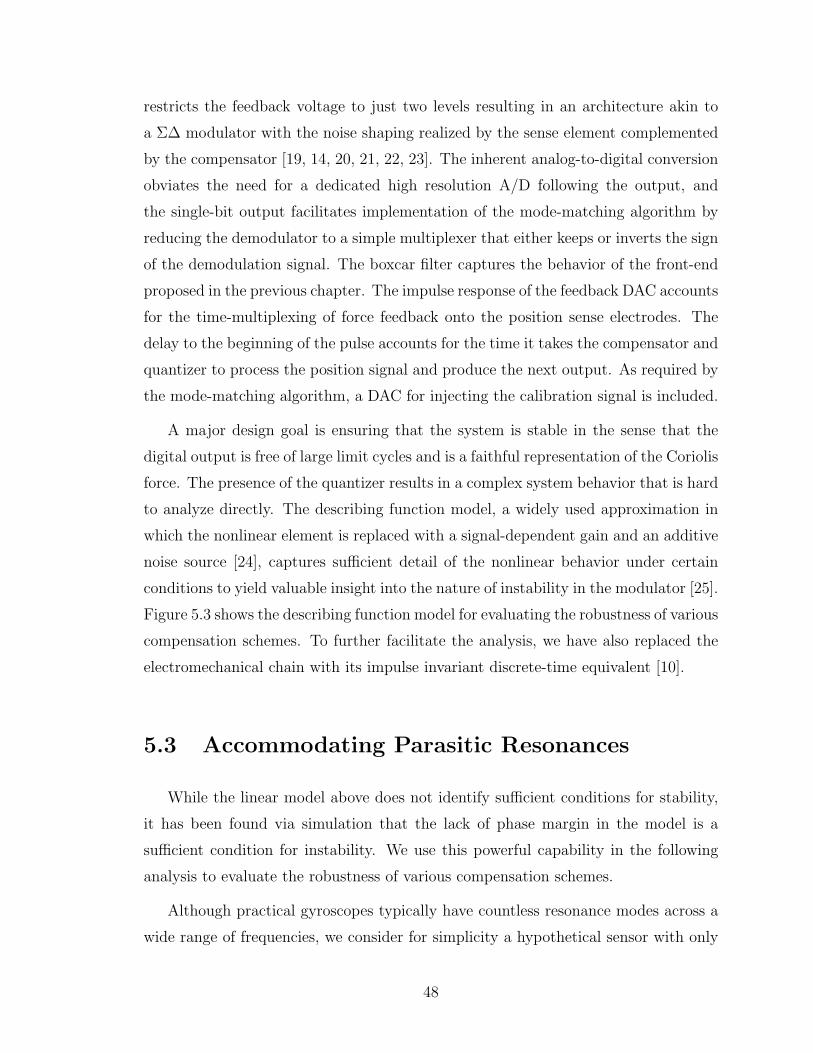
restricts the feedback voltage to just two levels resulting in an architecture akin to
a Σ∆ modulator with the noise shaping realized by the sense element complemented
by the compensator [19, 14, 20, 21, 22, 23]. The inherent analog-to-digital conversion
obviates the need for a dedicated high resolution A/D following the output, and
the single-bit output facilitates implementation of the mode-matching algorithm by
reducing the demodulator to a simple multiplexer that either keeps or inverts the sign
of the demodulation signal. The boxcar filter captures the behavior of the front-end
proposed in the previous chapter. The impulse response of the feedback DAC accounts
for the time-multiplexing of force feedback onto the position sense electrodes. The
delay to the beginning of the pulse accounts for the time it takes the compensator and
quantizer to process the position signal and produce the next output. As required by
the mode-matching algorithm, a DAC for injecting the calibration signal is included.
A major design goal is ensuring that the system is stable in the sense that the
digital output is free of large limit cycles and is a faithful representation of the Coriolis
force. The presence of the quantizer results in a complex system behavior that is hard
to analyze directly. The describing function model, a widely used approximation in
which the nonlinear element is replaced with a signal-dependent gain and an additive
noise source [24], captures sufficient detail of the nonlinear behavior under certain
conditions to yield valuable insight into the nature of instability in the modulator [25].
Figure 5.3 shows the describing function model for evaluating the robustness of various
compensation schemes. To further facilitate the analysis, we have also replaced the
electromechanical chain with its impulse invariant discrete-time equivalent [10].
5.3 Accommodating Parasitic Resonances
While the linear model above does not identify sufficient conditions for stability,
it has been found via simulation that the lack of phase margin in the model is a
sufficient condition for instability. We use this powerful capability in the following
analysis to evaluate the robustness of various compensation schemes.
Although practical gyroscopes typically have countless resonance modes across a
wide range of frequencies, we consider for simplicity a hypothetical sensor with only
48
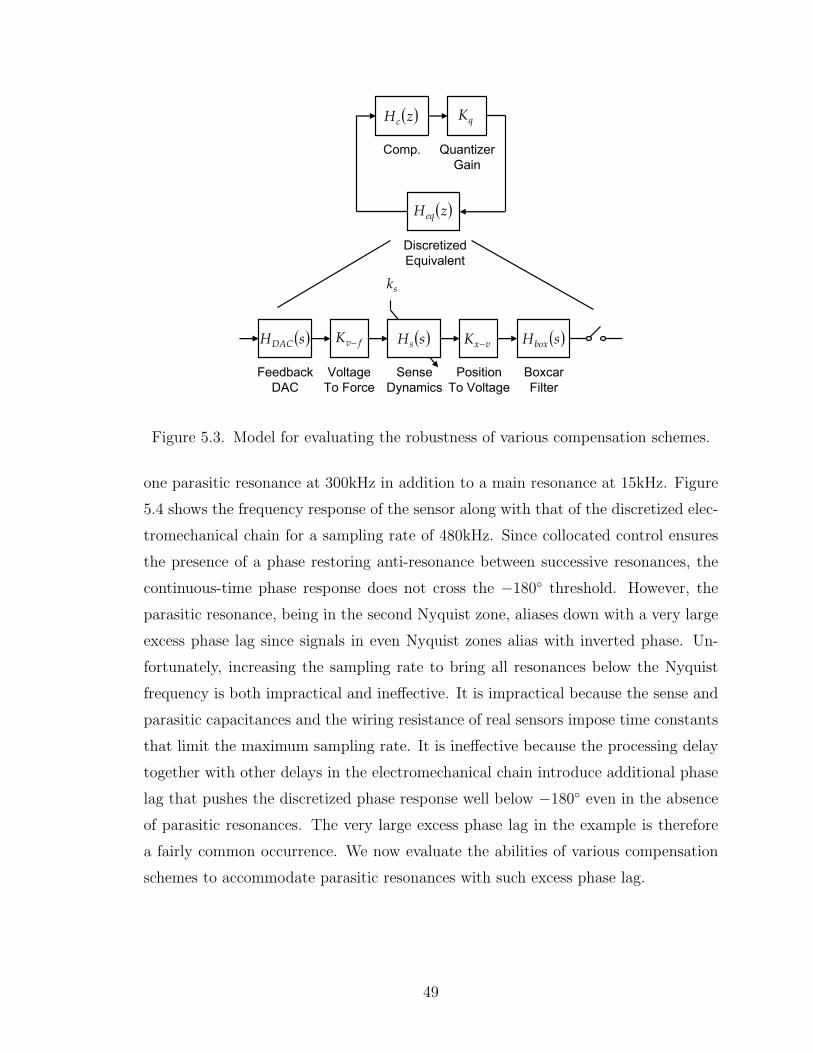
Comp.
( )zHc
Quantizer
Gain
Discretized
Equivalent
( )zH eq
qK
vxK −( )sHsfvK −
sk
Sense
Dynamics
( )sHbox
Boxcar
Filter
Voltage
To Force
Feedback
DAC
( )sHDAC
Position
To Voltage
Figure 5.3. Model for evaluating the robustness of various compensation schemes.
one parasitic resonance at 300kHz in addition to a main resonance at 15kHz. Figure
5.4 shows the frequency response of the sensor along with that of the discretized elec-
tromechanical chain for a sampling rate of 480kHz. Since collocated control ensures
the presence of a phase restoring anti-resonance between successive resonances, the
continuous-time phase response does not cross the −180 threshold. However, the
parasitic resonance, being in the second Nyquist zone, aliases down with a very large
excess phase lag since signals in even Nyquist zones alias with inverted phase. Un-
fortunately, increasing the sampling rate to bring all resonances below the Nyquist
frequency is both impractical and ineffective. It is impractical because the sense and
parasitic capacitances and the wiring resistance of real sensors impose time constants
that limit the maximum sampling rate. It is ineffective because the processing delay
together with other delays in the electromechanical chain introduce additional phase
lag that pushes the discretized phase response well below −180 even in the absence
of parasitic resonances. The very large excess phase lag in the example is therefore
a fairly common occurrence. We now evaluate the abilities of various compensation
schemes to accommodate parasitic resonances with such excess phase lag.
49
Excess Lag
Aliased
Resonance
Frequency
(kHz)
Normalized
Magnitude
(dB)
Phase
(°)
Excess Lag
Aliased
Resonance
Frequency
(kHz)
Normalized
Magnitude
(dB)
Phase
(°)
Figure 5.4. Frequency responses of a sensor with a parasitic resonance at 300kHz thataliases down to 180kHz with increased excess phase lag in the discretized frequencyresponse.
5.3.1 Traditional Lead Compensation
Readout interfaces employing Σ∆ force feedback must reject the quantization
noise in the desired signal band to a very high degree to satisfy stringent resolution
requirements. Because the frequency shaping provided by the sense element alone is
always insufficient to reject quantization noise to a level below that set by the posi-
tion sense front-end [10], the widely used second-order modulator, the architecture in
which the sense element is the sole provider of frequency shaping and the compen-
sator only supplies phase lead, always has a degraded SNR. The degradation can be
quite substantial, for example 20dB in [23]. It is possible to realize a second-order ar-
chitecture that avoids the SNR degradation by using multi-bit rather than single-bit
quantization. Among the disadvantages of this approach are the difficulty of applying
the required multi-bit force-feedback in a way that is compatible with the previously
mentioned bang-bang control, the increased complexity of the demodulator used by
the mode-matching algorithm, and the increased complexity of the decimator used to
process the oversampled multi-bit output. Additional frequency shaping provided by
the compensator in the fourth-order modulator reported in [22] eliminates the SNR
50
degradation with minimal added complexity. We consider only the forth-order archi-
tecture since it preserves the SNR improvements with only a very modest increase in
the overall system complexity.
The compensator used in the fourth-order architecture is of the form
Hc(z) =z + a
z︸ ︷︷ ︸lead
comp.
z2 + b1z + b2
z2 + cz + 1︸ ︷︷ ︸frequencyshaping
. (5.2)
The pair of imaginary poles controlled by c provides the above mentioned frequency
shaping, and the pair of complex zeros controlled by b1 and b2 compensates the phase
lag of the imaginary poles. The zero at a provides phase lead at high frequencies
to compensate the phase lag of the discretized system. The pole at the origin, un-
avoidable since a physically realizable system cannot have more zeros than poles,
unfortunately negates the phase lead provided by the zero, limiting the available
phase lead near the Nyquist frequency. Figure 5.5 shows the resulting open-loop fre-
quency response for typical coefficient values. As one might expect, the system is
stable without the parasitic resonance. With the parasitic resonance, however, the
system possesses three unity gain frequencies the last of which is characterized by
a large negative phase margin. Unfortunately, the system cannot be stabilized by
simply lowering the overall gain since doing so introduces negative phase margin at
a different frequency. Even after lowering the gain to a point where the available in-
band loop gain is far too low to be useful, the system remains unstable. Lacking the
large phase lead needed to accommodate high-Q parasitic resonances, compensators
of this kind are inadequate for practical vacuum packaged gyroscopes.
5.3.2 Positive Feedback Technique
A block whose output is simply the negative of the input is normally thought of
as introducing 180 of phase lag at all frequencies. Equally valid is thinking of the
block as introducing 180 of phase lead at all frequencies since e±jπ = −1. The 180
of phase lead is free to be exploited provided that the consequent positive feedback is
handled with care. To prevent the positive feedback from leading to instability, the
open-loop DC gain must be set below unity and a lag compensator must be included
51
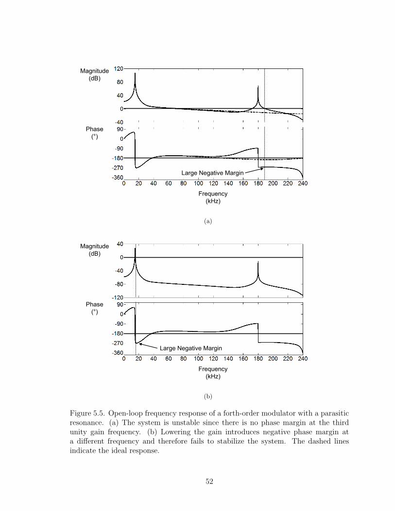
Frequency
(kHz)
Magnitude
(dB)
Phase
(°)
Large Negative Margin
Frequency
(kHz)
Magnitude
(dB)
Phase
(°)
Large Negative Margin
(a)
Frequency
(kHz)
Magnitude
(dB)
Phase
(°)
Large Negative Margin
Frequency
(kHz)
Magnitude
(dB)
Phase
(°)
Large Negative Margin
(b)
Figure 5.5. Open-loop frequency response of a forth-order modulator with a parasiticresonance. (a) The system is unstable since there is no phase margin at the thirdunity gain frequency. (b) Lowering the gain introduces negative phase margin ata different frequency and therefore fails to stabilize the system. The dashed linesindicate the ideal response.
52
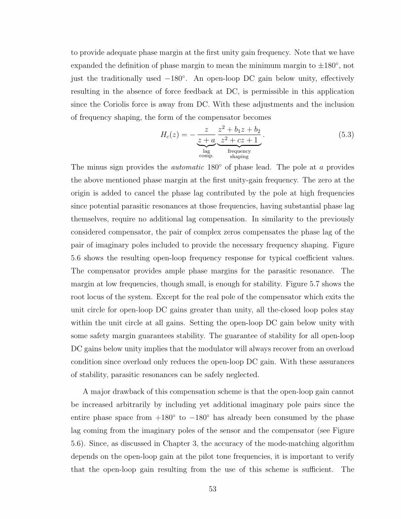
to provide adequate phase margin at the first unity gain frequency. Note that we have
expanded the definition of phase margin to mean the minimum margin to ±180, not
just the traditionally used −180. An open-loop DC gain below unity, effectively
resulting in the absence of force feedback at DC, is permissible in this application
since the Coriolis force is away from DC. With these adjustments and the inclusion
of frequency shaping, the form of the compensator becomes
Hc(z) = − z
z + a︸ ︷︷ ︸lag
comp.
z2 + b1z + b2
z2 + cz + 1︸ ︷︷ ︸frequencyshaping
. (5.3)
The minus sign provides the automatic 180 of phase lead. The pole at a provides
the above mentioned phase margin at the first unity-gain frequency. The zero at the
origin is added to cancel the phase lag contributed by the pole at high frequencies
since potential parasitic resonances at those frequencies, having substantial phase lag
themselves, require no additional lag compensation. In similarity to the previously
considered compensator, the pair of complex zeros compensates the phase lag of the
pair of imaginary poles included to provide the necessary frequency shaping. Figure
5.6 shows the resulting open-loop frequency response for typical coefficient values.
The compensator provides ample phase margins for the parasitic resonance. The
margin at low frequencies, though small, is enough for stability. Figure 5.7 shows the
root locus of the system. Except for the real pole of the compensator which exits the
unit circle for open-loop DC gains greater than unity, all the-closed loop poles stay
within the unit circle at all gains. Setting the open-loop DC gain below unity with
some safety margin guarantees stability. The guarantee of stability for all open-loop
DC gains below unity implies that the modulator will always recover from an overload
condition since overload only reduces the open-loop DC gain. With these assurances
of stability, parasitic resonances can be safely neglected.
A major drawback of this compensation scheme is that the open-loop gain cannot
be increased arbitrarily by including yet additional imaginary pole pairs since the
entire phase space from +180 to −180 has already been consumed by the phase
lag coming from the imaginary poles of the sensor and the compensator (see Figure
5.6). Since, as discussed in Chapter 3, the accuracy of the mode-matching algorithm
depends on the open-loop gain at the pilot tone frequencies, it is important to verify
that the open-loop gain resulting from the use of this scheme is sufficient. The
53
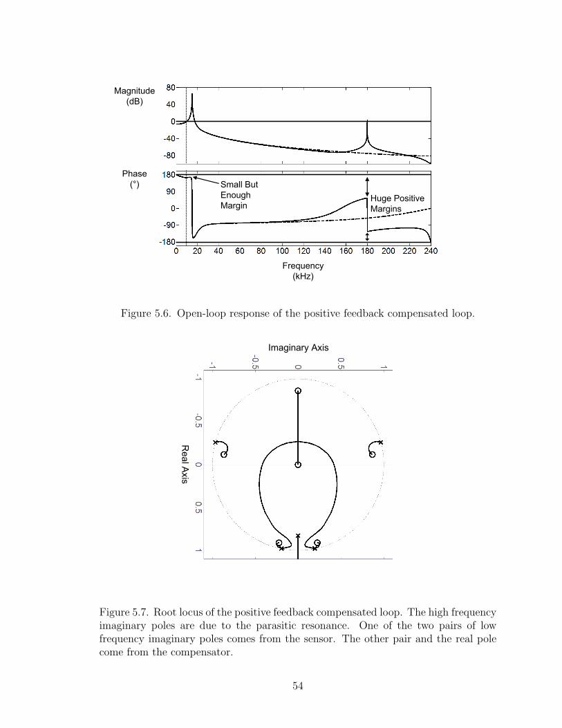
Frequency
(kHz)
Magnitude
(dB)
Phase
(°) Small But
Enough
MarginHuge Positive
Margins
Frequency
(kHz)
Magnitude
(dB)
Phase
(°) Small But
Enough
MarginHuge Positive
Margins
Figure 5.6. Open-loop response of the positive feedback compensated loop.
Real Axis
Imaginary Axis
Real Axis
Imaginary Axis
Figure 5.7. Root locus of the positive feedback compensated loop. The high frequencyimaginary poles are due to the parasitic resonance. One of the two pairs of lowfrequency imaginary poles comes from the sensor. The other pair and the real polecome from the compensator.
54
maximum achievable open-loop gain at a frequency offset ∆f from the drive frequency
is given by
Gmax =d
4
(fd∆f
)2
(5.4)
where d is a correction factor with a typical value of 0.25 to account for the less than
unity DC gain and the in-band gain reduction coming from the real pole and pair
of complex zeros of the compensator. The achievable gain of 47dB at a 250Hz offset
from 15kHz surpasses the open-loop gain requirement in the experimental prototype.
5.4 Positive Feedback Architecture
A practical positive feedback based Σ∆ architecture must be capable of forcing
the open-loop DC gain below unity and must be tolerant of potential offsets in the
sensor. In this section, we derive one such architecture.
5.4.1 Setting the Open-Loop DC Gain
Scaling the signal levels in the force feedback loop does nothing to the open-
loop gain because the quantizer gain simply adjusts to keep it constant. Since, as
mentioned previously, the quantizer gain is signal dependent, it is possible to force
the DC gain below unity by injecting an appropriate amount of dither before the
quantizer. Since the input variance of the quantizer increases while the output remains
constant, the quantizer gain decreases, lowering with it the open-loop gain. A pseudo-
random binary sequence is a good dither signal since it also helps to remove the
tonal behavior of the modulator and is easily generated using a linear feedback shift
register. The sequence does not degrade the overall interface noise floor since, like
the quantization noise, it appears at the output frequency-shaped by both the sensor
and the compensator. The dither signal can also be injected before the compensator,
in which case it is important to inject dither that has undergone frequency-shaping
to makeup for the loss of frequency shaping by the compensator. Figure 5.8 shows
the alternative solutions. In the experimental prototype, the dither is injected before
the compensator to reuse the DAC used to inject the calibration signal.
55
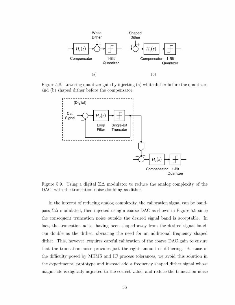
Compensator
( )zHc
1-Bit
Quantizer
White
Dither
(a)
Compensator
( )zHc
1-Bit
Quantizer
Shaped
Dither
(b)
Figure 5.8. Lowering quantizer gain by injecting (a) white dither before the quantizer,and (b) shaped dither before the compensator.
Compensator
( )zHc
1-Bit
Quantizer
Cal.
Signal( )zHd
Loop
Filter
Single-Bit
Truncator
(Digital)
Figure 5.9. Using a digital Σ∆ modulator to reduce the analog complexity of theDAC, with the truncation noise doubling as dither.
In the interest of reducing analog complexity, the calibration signal can be band-
pass Σ∆ modulated, then injected using a coarse DAC as shown in Figure 5.9 since
the consequent truncation noise outside the desired signal band is acceptable. In
fact, the truncation noise, having been shaped away from the desired signal band,
can double as the dither, obviating the need for an additional frequency shaped
dither. This, however, requires careful calibration of the coarse DAC gain to ensure
that the truncation noise provides just the right amount of dithering. Because of
the difficulty posed by MEMS and IC process tolerances, we avoid this solution in
the experimental prototype and instead add a frequency shaped dither signal whose
magnitude is digitally adjusted to the correct value, and reduce the truncation noise
56
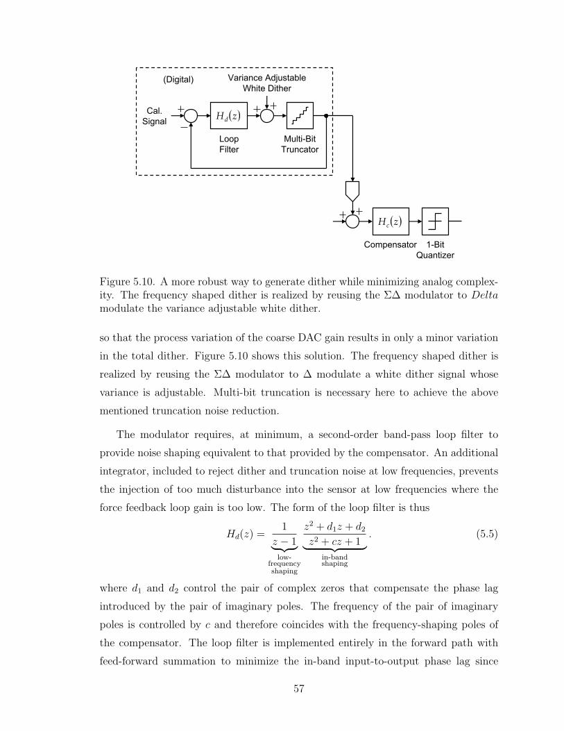
Compensator
( )zHc
1-Bit
Quantizer
Cal.
Signal( )zHd
Loop
Filter
Multi-Bit
Truncator
Variance Adjustable
White Dither(Digital)
Figure 5.10. A more robust way to generate dither while minimizing analog complex-ity. The frequency shaped dither is realized by reusing the Σ∆ modulator to Deltamodulate the variance adjustable white dither.
so that the process variation of the coarse DAC gain results in only a minor variation
in the total dither. Figure 5.10 shows this solution. The frequency shaped dither is
realized by reusing the Σ∆ modulator to ∆ modulate a white dither signal whose
variance is adjustable. Multi-bit truncation is necessary here to achieve the above
mentioned truncation noise reduction.
The modulator requires, at minimum, a second-order band-pass loop filter to
provide noise shaping equivalent to that provided by the compensator. An additional
integrator, included to reject dither and truncation noise at low frequencies, prevents
the injection of too much disturbance into the sensor at low frequencies where the
force feedback loop gain is too low. The form of the loop filter is thus
Hd(z) =1
z − 1︸ ︷︷ ︸low-
frequencyshaping
z2 + d1z + d2
z2 + cz + 1︸ ︷︷ ︸in-bandshaping
. (5.5)
where d1 and d2 control the pair of complex zeros that compensate the phase lag
introduced by the pair of imaginary poles. The frequency of the pair of imaginary
poles is controlled by c and therefore coincides with the frequency-shaping poles of
the compensator. The loop filter is implemented entirely in the forward path with
feed-forward summation to minimize the in-band input-to-output phase lag since
57
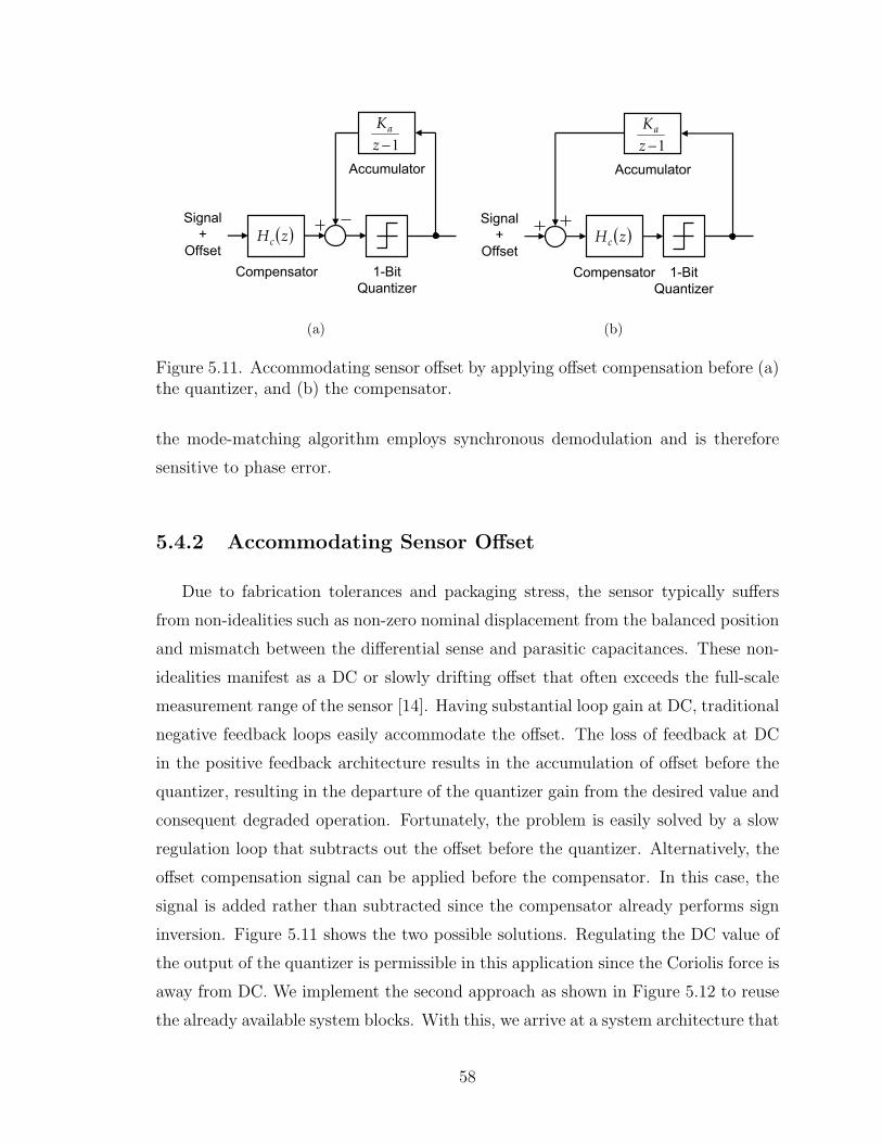
Compensator
( )zHc
1-Bit
Quantizer
Accumulator
1−z
Ka
Signal
+
Offset
(a)
Compensator
( )zHc
1-Bit
Quantizer
Accumulator
1−z
Ka
Signal
+
Offset
(b)
Figure 5.11. Accommodating sensor offset by applying offset compensation before (a)the quantizer, and (b) the compensator.
the mode-matching algorithm employs synchronous demodulation and is therefore
sensitive to phase error.
5.4.2 Accommodating Sensor Offset
Due to fabrication tolerances and packaging stress, the sensor typically suffers
from non-idealities such as non-zero nominal displacement from the balanced position
and mismatch between the differential sense and parasitic capacitances. These non-
idealities manifest as a DC or slowly drifting offset that often exceeds the full-scale
measurement range of the sensor [14]. Having substantial loop gain at DC, traditional
negative feedback loops easily accommodate the offset. The loss of feedback at DC
in the positive feedback architecture results in the accumulation of offset before the
quantizer, resulting in the departure of the quantizer gain from the desired value and
consequent degraded operation. Fortunately, the problem is easily solved by a slow
regulation loop that subtracts out the offset before the quantizer. Alternatively, the
offset compensation signal can be applied before the compensator. In this case, the
signal is added rather than subtracted since the compensator already performs sign
inversion. Figure 5.11 shows the two possible solutions. Regulating the DC value of
the output of the quantizer is permissible in this application since the Coriolis force is
away from DC. We implement the second approach as shown in Figure 5.12 to reuse
the already available system blocks. With this, we arrive at a system architecture that
58
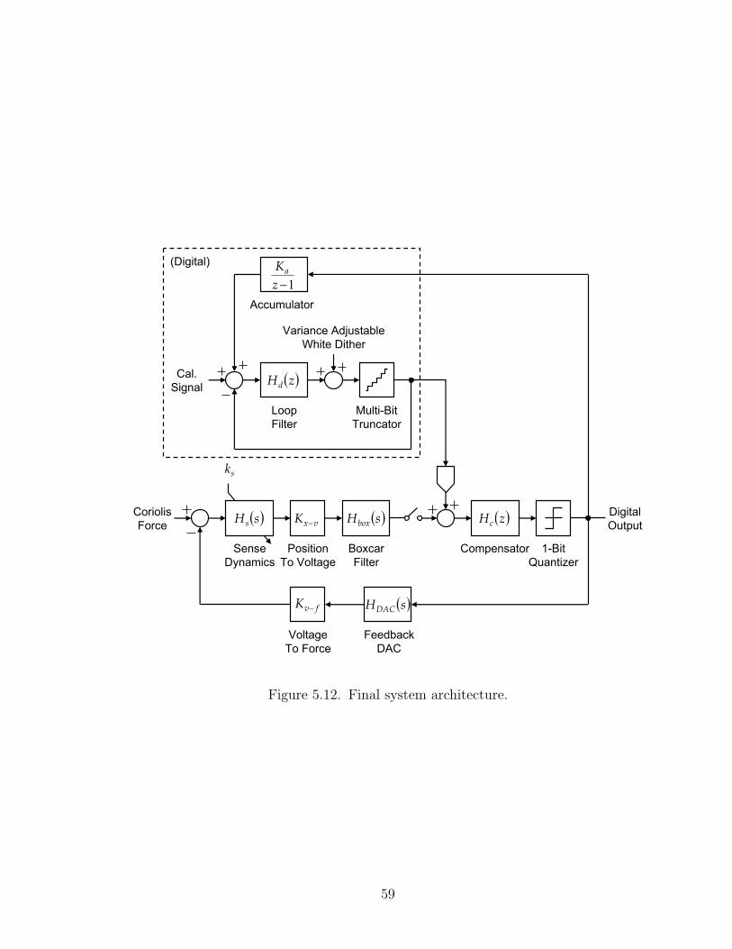
Compensator
( )zHc
1-Bit
Quantizer
Cal.
Signal( )zHd
Loop
Filter
Multi-Bit
Truncator
Variance Adjustable
White Dither
(Digital)
Accumulator
1−z
Ka
Coriolis
Force vxK −( )sHs
fvK −
sk
Sense
Dynamics
( )sHbox
Boxcar
Filter
Voltage
To Force
Digital
Output
Feedback
DAC
( )sHDAC
Position
To Voltage
Figure 5.12. Final system architecture.
59
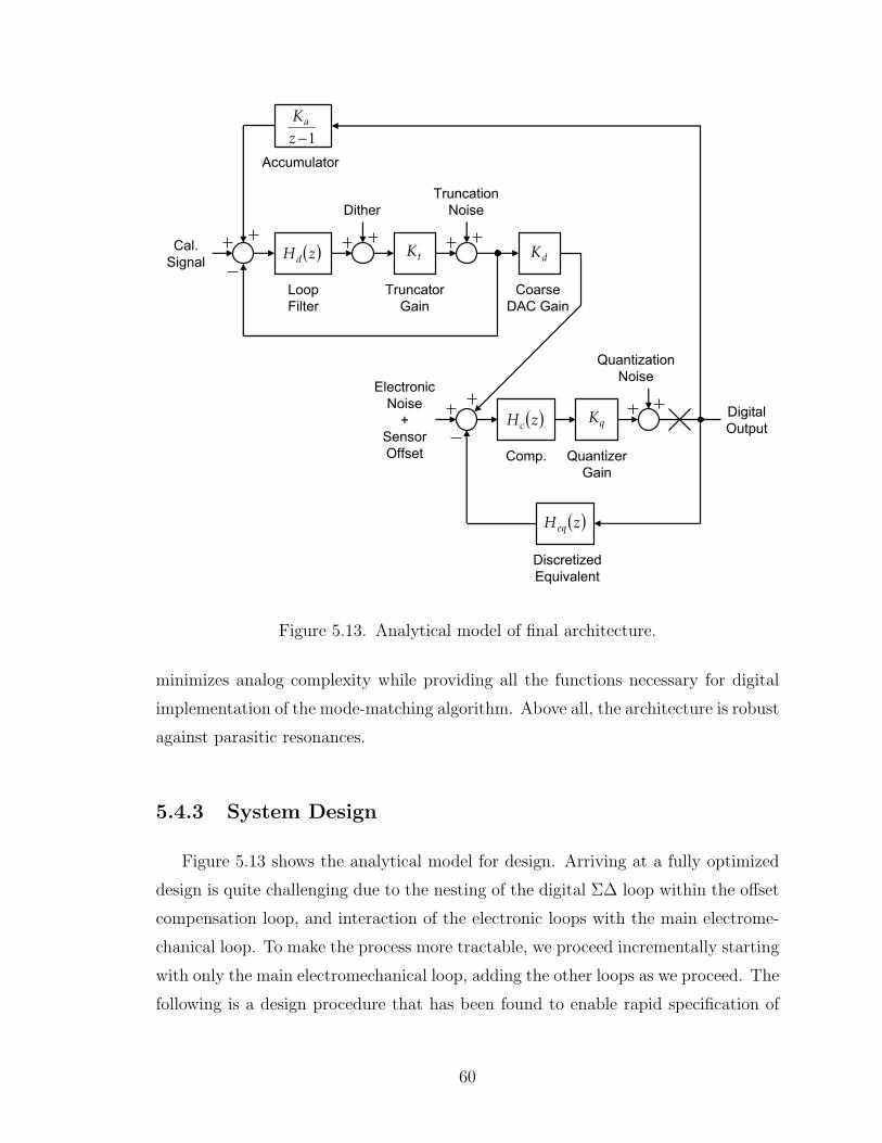
Comp.
( )zHc
Quantizer
Gain
Cal.
Signal( )zHd
Loop
Filter
Truncator
Gain
Accumulator
1−z
Ka
Discretized
Equivalent
( )zH eq
qK
dKtK
Coarse
DAC Gain
Digital
Output
Electronic
Noise
+
Sensor
Offset
Quantization
Noise
Truncation
NoiseDither
Figure 5.13. Analytical model of final architecture.
minimizes analog complexity while providing all the functions necessary for digital
implementation of the mode-matching algorithm. Above all, the architecture is robust
against parasitic resonances.
5.4.3 System Design
Figure 5.13 shows the analytical model for design. Arriving at a fully optimized
design is quite challenging due to the nesting of the digital Σ∆ loop within the offset
compensation loop, and interaction of the electronic loops with the main electrome-
chanical loop. To make the process more tractable, we proceed incrementally starting
with only the main electromechanical loop, adding the other loops as we proceed. The
following is a design procedure that has been found to enable rapid specification of
60
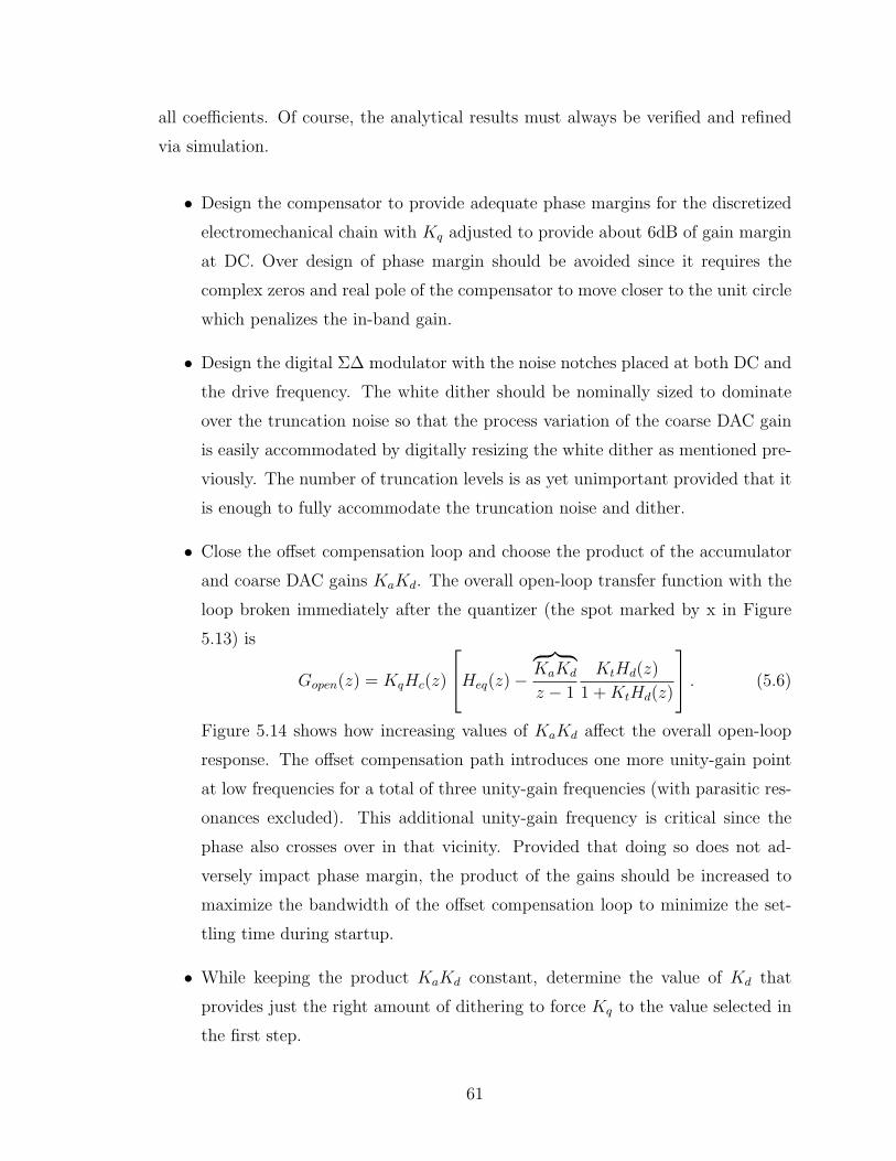
all coefficients. Of course, the analytical results must always be verified and refined
via simulation.
• Design the compensator to provide adequate phase margins for the discretized
electromechanical chain with Kq adjusted to provide about 6dB of gain margin
at DC. Over design of phase margin should be avoided since it requires the
complex zeros and real pole of the compensator to move closer to the unit circle
which penalizes the in-band gain.
• Design the digital Σ∆ modulator with the noise notches placed at both DC and
the drive frequency. The white dither should be nominally sized to dominate
over the truncation noise so that the process variation of the coarse DAC gain
is easily accommodated by digitally resizing the white dither as mentioned pre-
viously. The number of truncation levels is as yet unimportant provided that it
is enough to fully accommodate the truncation noise and dither.
• Close the offset compensation loop and choose the product of the accumulator
and coarse DAC gains KaKd. The overall open-loop transfer function with the
loop broken immediately after the quantizer (the spot marked by x in Figure
5.13) is
Gopen(z) = KqHc(z)
Heq(z)−︷ ︸︸ ︷KaKd
z − 1
KtHd(z)
1 +KtHd(z)
. (5.6)
Figure 5.14 shows how increasing values of KaKd affect the overall open-loop
response. The offset compensation path introduces one more unity-gain point
at low frequencies for a total of three unity-gain frequencies (with parasitic res-
onances excluded). This additional unity-gain frequency is critical since the
phase also crosses over in that vicinity. Provided that doing so does not ad-
versely impact phase margin, the product of the gains should be increased to
maximize the bandwidth of the offset compensation loop to minimize the set-
tling time during startup.
• While keeping the product KaKd constant, determine the value of Kd that
provides just the right amount of dithering to force Kq to the value selected in
the first step.
61
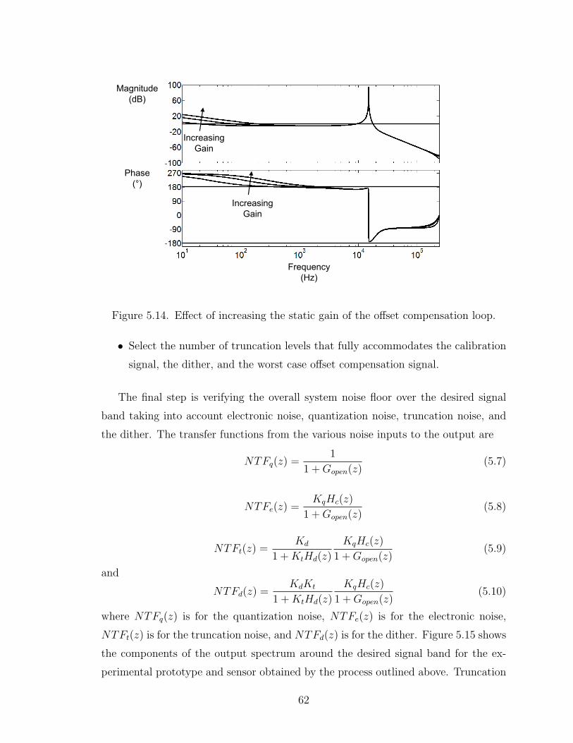
Frequency
(Hz)
Magnitude
(dB)
Phase
(°)
Increasing
Gain
Increasing
Gain
Frequency
(Hz)
Magnitude
(dB)
Phase
(°)
Increasing
Gain
Increasing
Gain
Figure 5.14. Effect of increasing the static gain of the offset compensation loop.
• Select the number of truncation levels that fully accommodates the calibration
signal, the dither, and the worst case offset compensation signal.
The final step is verifying the overall system noise floor over the desired signal
band taking into account electronic noise, quantization noise, truncation noise, and
the dither. The transfer functions from the various noise inputs to the output are
NTFq(z) =1
1 +Gopen(z)(5.7)
NTFe(z) =KqHc(z)
1 +Gopen(z)(5.8)
NTFt(z) =Kd
1 +KtHd(z)
KqHc(z)
1 +Gopen(z)(5.9)
and
NTFd(z) =KdKt
1 +KtHd(z)
KqHc(z)
1 +Gopen(z)(5.10)
where NTFq(z) is for the quantization noise, NTFe(z) is for the electronic noise,
NTFt(z) is for the truncation noise, and NTFd(z) is for the dither. Figure 5.15 shows
the components of the output spectrum around the desired signal band for the ex-
perimental prototype and sensor obtained by the process outlined above. Truncation
62
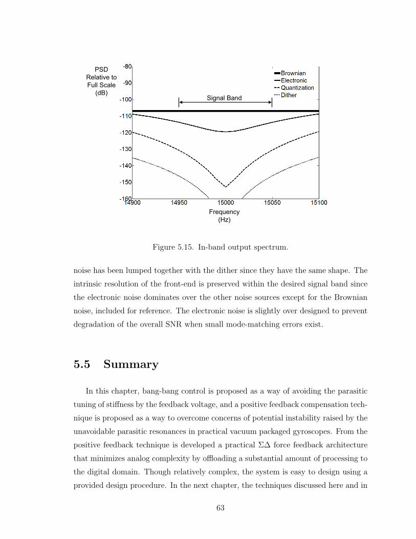
Frequency
(Hz)
PSD
Relative to
Full Scale
(dB)Signal Band
Frequency
(Hz)
PSD
Relative to
Full Scale
(dB)Signal Band
Figure 5.15. In-band output spectrum.
noise has been lumped together with the dither since they have the same shape. The
intrinsic resolution of the front-end is preserved within the desired signal band since
the electronic noise dominates over the other noise sources except for the Brownian
noise, included for reference. The electronic noise is slightly over designed to prevent
degradation of the overall SNR when small mode-matching errors exist.
5.5 Summary
In this chapter, bang-bang control is proposed as a way of avoiding the parasitic
tuning of stiffness by the feedback voltage, and a positive feedback compensation tech-
nique is proposed as a way to overcome concerns of potential instability raised by the
unavoidable parasitic resonances in practical vacuum packaged gyroscopes. From the
positive feedback technique is developed a practical Σ∆ force feedback architecture
that minimizes analog complexity by offloading a substantial amount of processing to
the digital domain. Though relatively complex, the system is easy to design using a
provided design procedure. In the next chapter, the techniques discussed here and in
63

previous chapters are applied towards the design of an experimental readout interface
for a high-Q micromachined vibratory gyroscope.
64
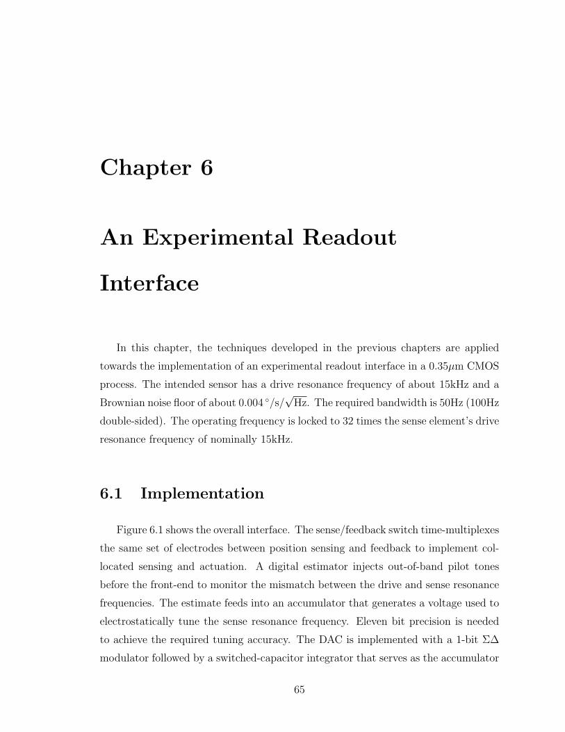
Chapter 6
An Experimental Readout
Interface
In this chapter, the techniques developed in the previous chapters are applied
towards the implementation of an experimental readout interface in a 0.35µm CMOS
process. The intended sensor has a drive resonance frequency of about 15kHz and a
Brownian noise floor of about 0.004 /s/√
Hz. The required bandwidth is 50Hz (100Hz
double-sided). The operating frequency is locked to 32 times the sense element’s drive
resonance frequency of nominally 15kHz.
6.1 Implementation
Figure 6.1 shows the overall interface. The sense/feedback switch time-multiplexes
the same set of electrodes between position sensing and feedback to implement col-
located sensing and actuation. A digital estimator injects out-of-band pilot tones
before the front-end to monitor the mismatch between the drive and sense resonance
frequencies. The estimate feeds into an accumulator that generates a voltage used to
electrostatically tune the sense resonance frequency. Eleven bit precision is needed
to achieve the required tuning accuracy. The DAC is implemented with a 1-bit Σ∆
modulator followed by a switched-capacitor integrator that serves as the accumulator
65
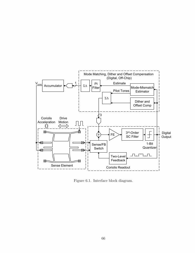
Sense/FB
Switch
FE
Two-Level
Feedback
3rd-Order
SC Filter
1-Bit
Quantizer
3
Accumulator
Σ∆
Dither and
Offset Comp
Mode-Mismatch
EstimatorPilot Tones
EstimateΣ∆
Vtune1
Digital
Output
Mode Matching, Dither and Offset Compensation
(Digital, Off-Chip)
Sense Element
Coriolis
Acceleration
Drive
Motion
PI
Filter
Coriolis Readout
Figure 6.1. Interface block diagram.
66
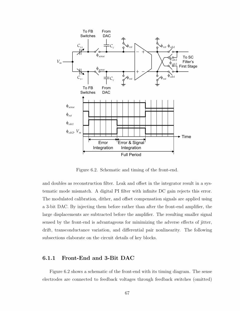
senseφ
From
DAC
From
DAC
To SC
Filter’s
First Stage
senseφ
rstφ
rstφ
rstφ
rstφ1cdsφ
1cdsφ
2cdsφ2cdsφ
−sC
+sC
cC
cC
To FB
Switches
To FB
Switches
mV
Error
Integration
Error & Signal
Integration
φrst
φsense
φcds2, Vm
φcds1
Full Period
Time
Figure 6.2. Schematic and timing of the front-end.
and doubles as reconstruction filter. Leak and offset in the integrator result in a sys-
tematic mode mismatch. A digital PI filter with infinite DC gain rejects this error.
The modulated calibration, dither, and offset compensation signals are applied using
a 3-bit DAC. By injecting them before rather than after the front-end amplifier, the
large displacements are subtracted before the amplifier. The resulting smaller signal
sensed by the front-end is advantageous for minimizing the adverse effects of jitter,
drift, transconductance variation, and differential pair nonlinearity. The following
subsections elaborate on the circuit details of key blocks.
6.1.1 Front-End and 3-Bit DAC
Figure 6.2 shows a schematic of the front-end with its timing diagram. The sense
electrodes are connected to feedback voltages through feedback switches (omitted)
67
uC
To
Front-End
0d
0d
uC
1d
1d
uC
6d
6d
rstφ
mV
Figure 6.3. Simplified schematic of 3-bit DAC. Actual implementation is differential.
during the feedback phase and to the front-end amplifier through the sense switches
during the sense phase. The output of the amplifier is connected directly to the
following switched-capacitor filter through the CDS switches during the two integra-
tion phases and reset to ground when the front-end is inactive. The output of the
3-bit DAC is capacitively coupled to the input of the amplifier. The coupling ca-
pacitor is only 70fF, negligible compared to the 8pF of combined sense and parasitic
capacitances.
Figure 6.3 shows the 3-bit DAC. It is shown as single-ended for simplicity, but
the actual implementation is differential. It consists of seven unit elements that,
depending on the input code, are connected to either ground or the proof mass node.
When the pulse is applied on the proof mass, a voltage proportional to the capacitance
imbalance between the sense capacitors, together with a voltage dependent on the
input code of the DAC, develops at the input of the amplifier. The proof mass and
DAC are excited by the same voltage pulse to keep the displacement to voltage gain
and the DAC gain ratiometric.
Figure 6.4 shows the transistor-level circuit diagram of the front-end OTA. A
folded cascode with PMOS inputs is chosen to enable an input common-mode level
of Vss (since the sense electrode are reset in preparation for position sensing). The
double cascodes provide high output impedance.
6.1.2 Compensator
The first step in implementing the compensator is the synthesis of the transfer
function out of only unit delay and gain elements. Figure 6.5 shows a realization that
68
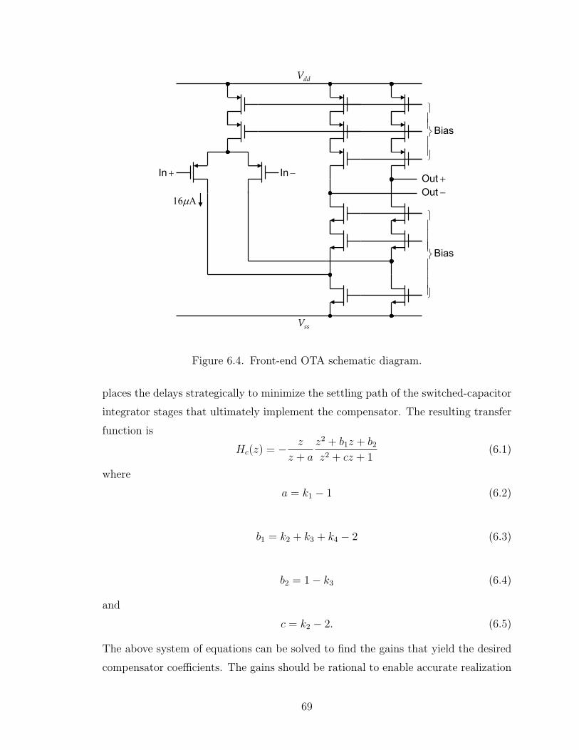
+In+Out
ddV
ssV
A16µ
Bias
−Out
−In
Bias
Figure 6.4. Front-end OTA schematic diagram.
places the delays strategically to minimize the settling path of the switched-capacitor
integrator stages that ultimately implement the compensator. The resulting transfer
function is
Hc(z) = − z
z + a
z2 + b1z + b2
z2 + cz + 1(6.1)
where
a = k1 − 1 (6.2)
b1 = k2 + k3 + k4 − 2 (6.3)
b2 = 1− k3 (6.4)
and
c = k2 − 2. (6.5)
The above system of equations can be solved to find the gains that yield the desired
compensator coefficients. The gains should be rational to enable accurate realization
69
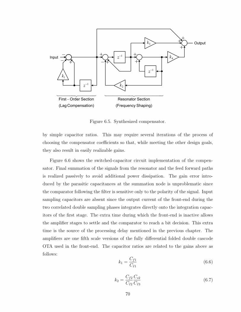
Output
Input
1k
1−z
1−z
1−z
2k
4k
3k
4444 34444 21
on)Compensati (Lag
Section OrderFirst −
444444 3444444 21
Shaping) (Frequency
Section Resonator
Figure 6.5. Synthesized compensator.
by simple capacitor ratios. This may require several iterations of the process of
choosing the compensator coefficients so that, while meeting the other design goals,
they also result in easily realizable gains.
Figure 6.6 shows the switched-capacitor circuit implementation of the compen-
sator. Final summation of the signals from the resonator and the feed forward paths
is realized passively to avoid additional power dissipation. The gain error intro-
duced by the parasitic capacitances at the summation node is unproblematic since
the comparator following the filter is sensitive only to the polarity of the signal. Input
sampling capacitors are absent since the output current of the front-end during the
two correlated double sampling phases integrates directly onto the integration capac-
itors of the first stage. The extra time during which the front-end is inactive allows
the amplifier stages to settle and the comparator to reach a bit decision. This extra
time is the source of the processing delay mentioned in the previous chapter. The
amplifiers are one fifth scale versions of the fully differential folded double cascode
OTA used in the front-end. The capacitor ratios are related to the gains above as
follows:
k1 =Cf1
CI1(6.6)
k2 =Cf2
CI2
Cs2CI3
(6.7)
70
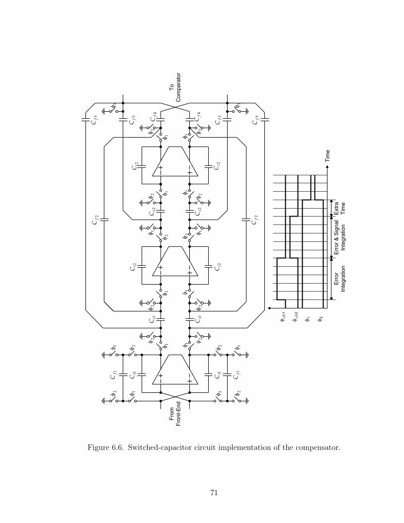
Error
Integration
Error & Signal
Integration
φcds2
φcds1
φ2
φ1
Time
Extra
Time
1φ
1iC
1iC
1fC
1fC
2φ
2φ
1φ
2φ
1φ
1φ
2φ
1φ
1φ
2φ
2φ
2φ
2φ
1φ
1φ
1sC
1sC
2iC
2iC
1φ
1φ
2φ
2φ
1φ
1φ
2φ
2φ
2sC
2sC
2iC
2iC
2f
C
2f
C
1φ
1φ
2φ
2φ
1φ
1φ
4f
C
3f
C
3f
C
5f
C
5f
C
4f
C
From
Front-End
To
Comparator
Figure 6.6. Switched-capacitor circuit implementation of the compensator.
71
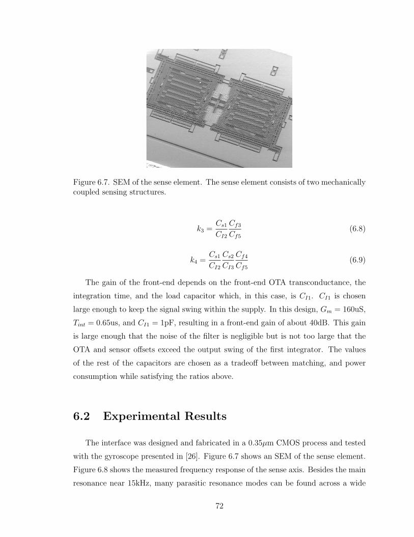
Figure 6.7. SEM of the sense element. The sense element consists of two mechanicallycoupled sensing structures.
k3 =Cs1CI2
Cf3
Cf5
(6.8)
k4 =Cs1CI2
Cs2CI3
Cf4
Cf5
(6.9)
The gain of the front-end depends on the front-end OTA transconductance, the
integration time, and the load capacitor which, in this case, is CI1. CI1 is chosen
large enough to keep the signal swing within the supply. In this design, Gm = 160uS,
Tint = 0.65us, and CI1 = 1pF, resulting in a front-end gain of about 40dB. This gain
is large enough that the noise of the filter is negligible but is not too large that the
OTA and sensor offsets exceed the output swing of the first integrator. The values
of the rest of the capacitors are chosen as a tradeoff between matching, and power
consumption while satisfying the ratios above.
6.2 Experimental Results
The interface was designed and fabricated in a 0.35µm CMOS process and tested
with the gyroscope presented in [26]. Figure 6.7 shows an SEM of the sense element.
Figure 6.8 shows the measured frequency response of the sense axis. Besides the main
resonance near 15kHz, many parasitic resonance modes can be found across a wide
72
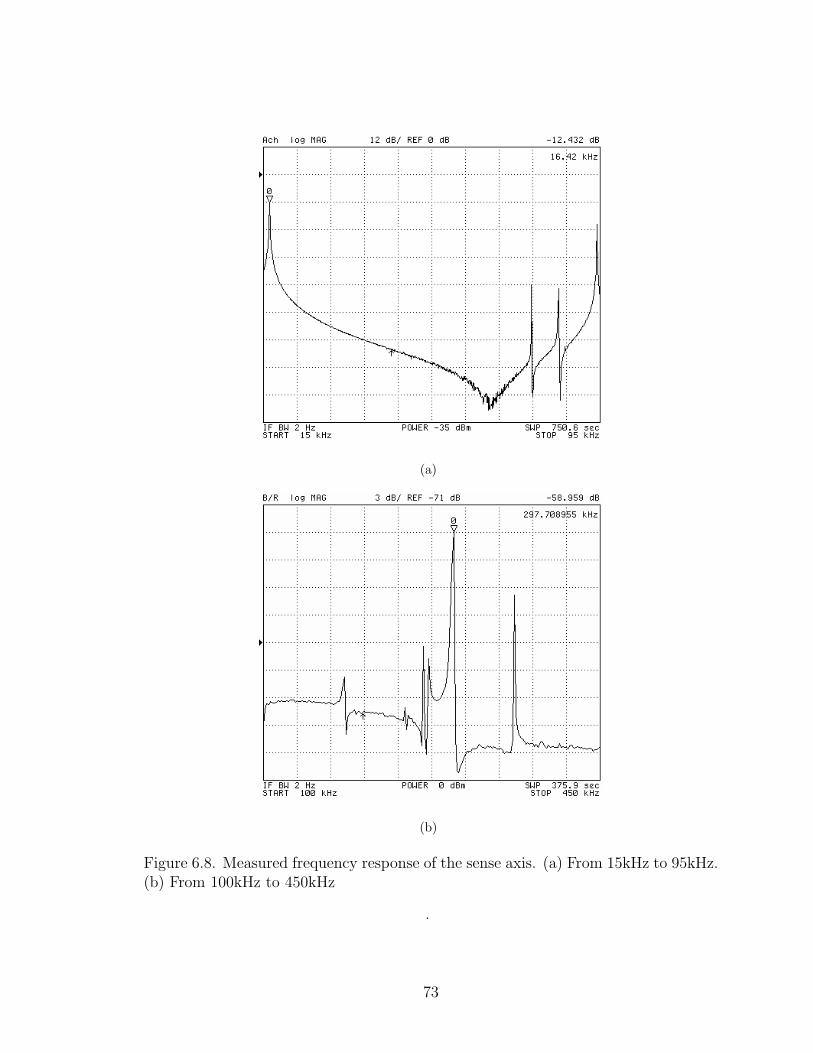
(a)
(b)
Figure 6.8. Measured frequency response of the sense axis. (a) From 15kHz to 95kHz.(b) From 100kHz to 450kHz
.
73
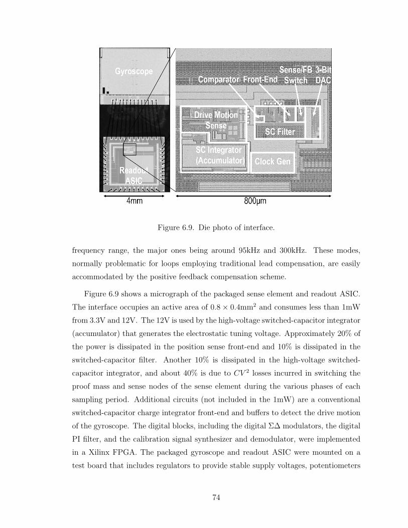
Figure 6.9. Die photo of interface.
frequency range, the major ones being around 95kHz and 300kHz. These modes,
normally problematic for loops employing traditional lead compensation, are easily
accommodated by the positive feedback compensation scheme.
Figure 6.9 shows a micrograph of the packaged sense element and readout ASIC.
The interface occupies an active area of 0.8× 0.4mm2 and consumes less than 1mW
from 3.3V and 12V. The 12V is used by the high-voltage switched-capacitor integrator
(accumulator) that generates the electrostatic tuning voltage. Approximately 20% of
the power is dissipated in the position sense front-end and 10% is dissipated in the
switched-capacitor filter. Another 10% is dissipated in the high-voltage switched-
capacitor integrator, and about 40% is due to CV 2 losses incurred in switching the
proof mass and sense nodes of the sense element during the various phases of each
sampling period. Additional circuits (not included in the 1mW) are a conventional
switched-capacitor charge integrator front-end and buffers to detect the drive motion
of the gyroscope. The digital blocks, including the digital Σ∆ modulators, the digital
PI filter, and the calibration signal synthesizer and demodulator, were implemented
in a Xilinx FPGA. The packaged gyroscope and readout ASIC were mounted on a
test board that includes regulators to provide stable supply voltages, potentiometers
74
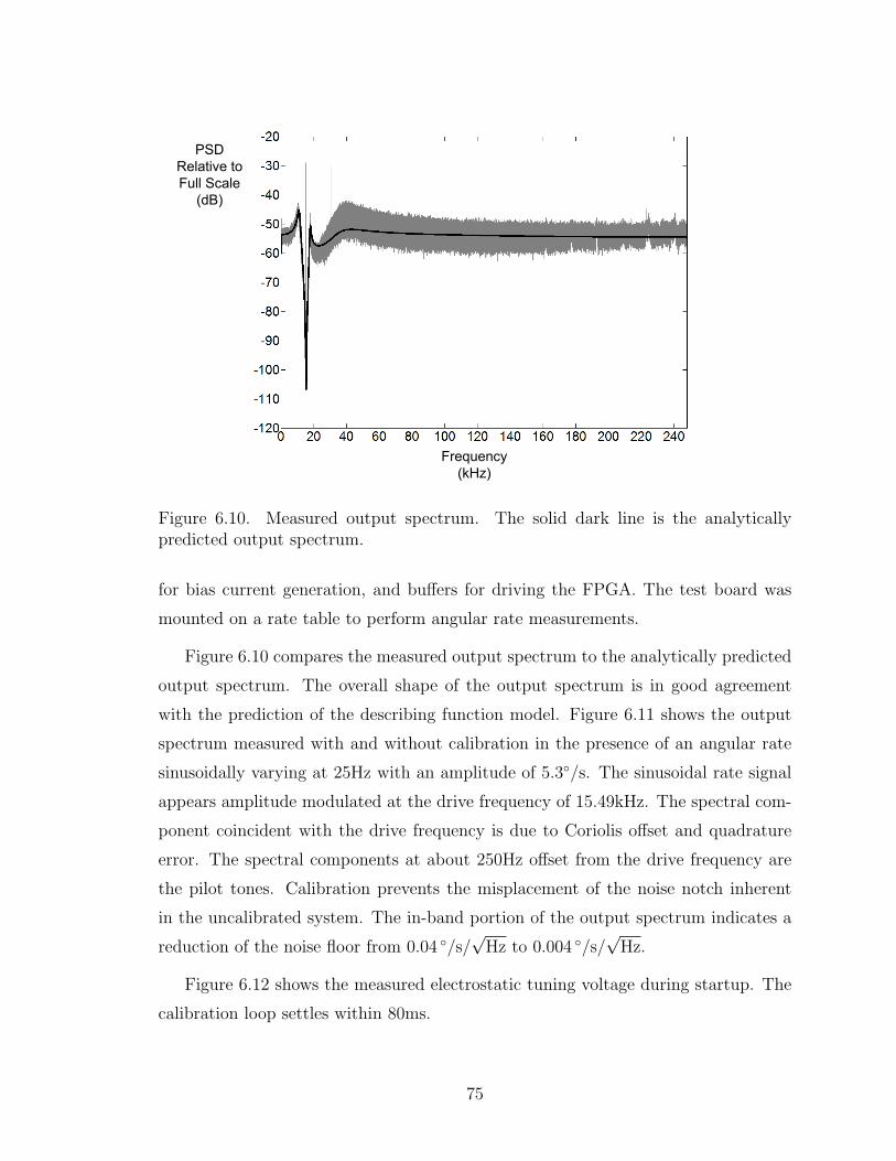
Frequency
(kHz)
PSD
Relative to
Full Scale
(dB)
Frequency
(kHz)
PSD
Relative to
Full Scale
(dB)
Figure 6.10. Measured output spectrum. The solid dark line is the analyticallypredicted output spectrum.
for bias current generation, and buffers for driving the FPGA. The test board was
mounted on a rate table to perform angular rate measurements.
Figure 6.10 compares the measured output spectrum to the analytically predicted
output spectrum. The overall shape of the output spectrum is in good agreement
with the prediction of the describing function model. Figure 6.11 shows the output
spectrum measured with and without calibration in the presence of an angular rate
sinusoidally varying at 25Hz with an amplitude of 5.3/s. The sinusoidal rate signal
appears amplitude modulated at the drive frequency of 15.49kHz. The spectral com-
ponent coincident with the drive frequency is due to Coriolis offset and quadrature
error. The spectral components at about 250Hz offset from the drive frequency are
the pilot tones. Calibration prevents the misplacement of the noise notch inherent
in the uncalibrated system. The in-band portion of the output spectrum indicates a
reduction of the noise floor from 0.04 /s/√
Hz to 0.004 /s/√
Hz.
Figure 6.12 shows the measured electrostatic tuning voltage during startup. The
calibration loop settles within 80ms.
75
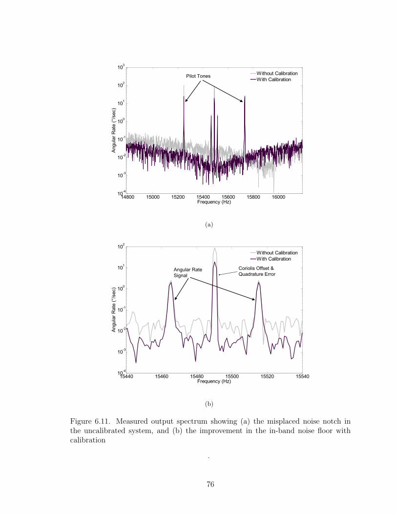
14800 15000 15200 15400 15600 15800 1600010-4
10-3
10-2
10-1
100
101
102
103
Frequency (Hz)
Angular Rate (°/sec)
Without Calibration
With CalibrationPilot Tones
14800 15000 15200 15400 15600 15800 1600010-4
10-3
10-2
10-1
100
101
102
103
Frequency (Hz)
Angular Rate (°/sec)
Without Calibration
With CalibrationPilot Tones
(a)
15440 15460 15480 15500 15520 1554010-4
10-3
10-2
10-1
100
101
102
Frequency (Hz)
Angular Rate (°/sec)
Without Calibration
With Calibration
Angular Rate
Signal
Coriolis Offset &
Quadrature Error
15440 15460 15480 15500 15520 1554010-4
10-3
10-2
10-1
100
101
102
Frequency (Hz)
Angular Rate (°/sec)
Without Calibration
With Calibration
Angular Rate
Signal
Coriolis Offset &
Quadrature Error
(b)
Figure 6.11. Measured output spectrum showing (a) the misplaced noise notch inthe uncalibrated system, and (b) the improvement in the in-band noise floor withcalibration
.
76
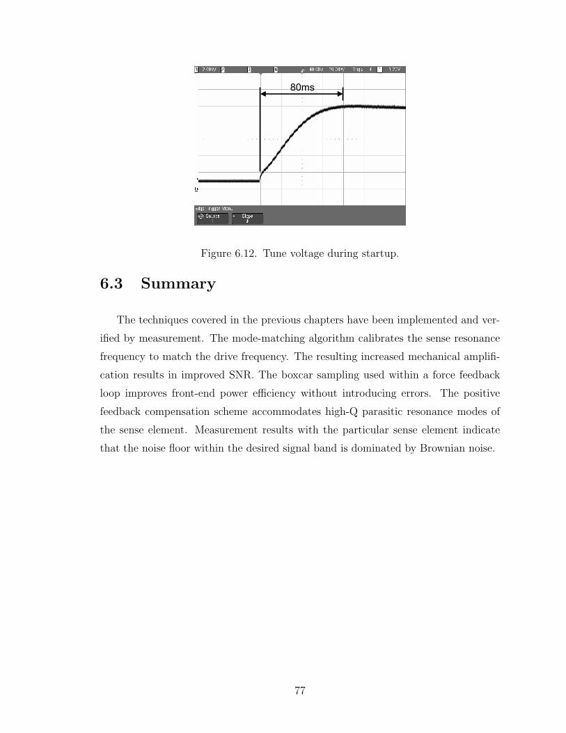
80ms
Figure 6.12. Tune voltage during startup.
6.3 Summary
The techniques covered in the previous chapters have been implemented and ver-
ified by measurement. The mode-matching algorithm calibrates the sense resonance
frequency to match the drive frequency. The resulting increased mechanical amplifi-
cation results in improved SNR. The boxcar sampling used within a force feedback
loop improves front-end power efficiency without introducing errors. The positive
feedback compensation scheme accommodates high-Q parasitic resonance modes of
the sense element. Measurement results with the particular sense element indicate
that the noise floor within the desired signal band is dominated by Brownian noise.
77
Chapter 7
Conclusions
7.1 Results
Matching the drive and sense resonance frequencies of a vibratory gyroscope en-
ables substantial improvements in the power efficiency of the readout interface, but
implies certain architectural choices. This dissertation presents the architecture and
circuits used to exploit the sense resonance to achieve more than 30dB improvement
in the Coriolis acceleration noise floor over traditional solutions dissipating the same
amount of power. 20dB of the power savings comes from the mechanical amplification
provided by the sense resonance. The remaining 10dB comes from the use of boxcar
sampling.
The system architecture developed here uses background calibration to match the
drive and sense resonance frequencies beyond fabrication tolerances to enable the full
exploitation of the sense resonance. It uses force feedback to overcome challenges
such as limited sense bandwidth and poor scale factor stability brought about by
mode-matching. It uses bang-bang control to prevent the feedback voltage from
inadvertently tuning the sense resonance, and uses a positive feedback compensation
technique to ensure that the force feedback loop remains stable and robust against
the parasitic resonance modes of the sense element. The ultimate result is the first
78
experimentally verified 1mW gyroscope readout interface with a 0.004 /s/√
Hz noise
floor over a 50Hz band.
7.2 Future Work
With the several order-orders-of-magnitude improvement in the readout interface
power efficiency, the impact of the drive circuit power dissipation gains in signifi-
cance. Research into low-power drive circuits is therefore a logical next step. Besides
power dissipation, other important metrics for the drive circuit are the temperature
stability of the drive amplitude and the time from startup to steady-state oscillation.
Temperature stability is especially critical in inertial navigation applications where
the variation of the scale factor in the presence of a Coriolis offset can appear as a
large bias drift. The time from startup to steady-state oscillation is important in
image stabilization applications where the gyroscope is usually only briefly activated
when a picture is being taken. Achieving good temperature stability and fast startup
at much lower power than is used presently is one of the major challenges for future
research.
79
Bibliography
[1] W. A. Clark, Micromachined Vibratory Rate Gyroscopes. PhD thesis, ElectricalEngineering and Computer Sciences, University of California, Berkeley, 1997.
[2] J. A. Geen, S. J. Sherman, J. F. Chang, and S. R. Lewis, “Single-chip surfacemicromachined integrated gyroscope with 50/h Allan deviation,” IEEE Journalof Solid-State Circuits, vol. 37, pp. 1860–1866, Dec. 2002.
[3] W. A. Clark, R. T. Howe, and R. Horowitz, “Surface micromachined Z-axisvibratory rate gyroscope,” in Technical Digest of the Solid-State Sensor andActuator Workshop, (Hilton Head Island, SC), pp. 283–287, 1996.
[4] M. S. Weinberg and A. Kourepenis, “Error sources in in-plane silicon tuning-fork MEMS gyroscopes,” Journal of Microelectromechanical Systems, vol. 15,pp. 479–491, June 2006.
[5] M. W. Putty and K. Najafi, “A micromachined vibrating ring gyroscope,” inTechnical Digest of the Solid-State Sensor and Actuator Workshop, (Hilton HeadIsland, SC), pp. 213–220, 1994.
[6] J. Choi, K. Minami, and M. Esashi, “Silicon resonant angular rate sensor byreactive ion etching,” in Technical Digest of the 13th Sensor Symposium, (Tokyo,Japan), pp. 177–180, 1995.
[7] W. Yun, R. T. Howe, and P. R. Gray, “Surface micromachined, digitally force-balanced accelerometer with integrated CMOS detection circuitry,” in TechnicalDigest of the Solid-State Sensor and Actuator Workshop, (Hilton Head Island,SC), pp. 126–131, 1992.
[8] Analog Devices, One Technology Way, Norwood, MA 02062, ADXL50: Mono-lithic accelerometer with signal conditioning.
[9] A. Sharma, M. Zaman, and F. Ayazi, “A 0.2/hr mirco-gyroscope with automaticCMOS mode matching,” in ISSCC Digest of Technical Papers, (San Fransisco,CA), pp. 386–387, 2007.
[10] X. Jiang, Capacitive Position-Sensing Interface for Micromachined Inertial Sen-sors. PhD thesis, Electrical Engineering and Computer Sciences, University ofCalifornia, Berkeley, 2003.
80
[11] V. P. Petkov, High-Order Σ∆ Interface for Micromachined Inertial Sensors. PhDthesis, Electrical Engineering and Computer Sciences, University of California,Berkeley, 2004.
[12] J. I. Seeger, X. Jiang, M. Kraft, and B. E. Boser, “Sense finger dynamics in aΣ∆ force-feedback gyroscope,” in Technical Digest of the Solid-State Sensor andActuator Workshop, (Hilton Head Island, SC), pp. 296–299, 2000.
[13] A. Preumont, Vibration Control of Active Structures: An Introduction. KluwerAcademic Publishers, 2nd ed., 2002.
[14] M. Lemkin and B. E. Boser, “A three-axis micromachined accelerometer with aCMOS position-sense interface and digital offset-trim electronics,” IEEE Journalof Solid-State Circuits, vol. 34, pp. 456–468, Apr. 1999.
[15] J. Wu, G. K. Fedder, and L. R. Carley, “A low-noise low-offset capacitive sens-ing amplifier for a 50-µg/
√Hz monolithic CMOS MEMS accelerometer,” IEEE
Journal of Solid-State Circuits, vol. 39, pp. 722–730, May 2004.
[16] C. C. Enz and G. C. Temes, “Circuit techniques for reducing the effects ofop-amp imperfections: autozeroing, correlated double sampling, and chopperstabilization,” Proceedings of the IEEE, vol. 84, pp. 1584–1614, Nov. 1996.
[17] M. Lemkin, Micro Accelerometer Design with Digital Feedback Control. PhDthesis, Electrical Engineering and Computer Sciences, University of California,Berkeley, 1997.
[18] C. Lang and R. Tielert, “A low noise accelerometer with digital PID-type con-troller and multibit force feedback,” in Proceedings of the 25th European Solid-State Circuits Conference, (Neuily sur Seine, France), pp. 250–253, 1999.
[19] T. Smith, O. Nys, M. Chevroulet, Y. DeCoulon, and M. Degrauwe, “A 15b elec-tromechanical sigma-delta converter for acceleration measurements,” in ISSCCDigest of Technical Papers, (San Fransisco, CA), pp. 160–161, 1994.
[20] X. Jiang, J. I. Seeger, M. Kraft, and B. E. Boser, “A monolithic surface micro-machined Z-axis gyroscope with digital output,” in Symposium on VLSI CircuitsDigest of Technical Papers, (Honolulu, HI), pp. 16–19, 2000.
[21] H. Kulah, A. Salian, N. Yazdi, and K. Najafi, “A 5V closed-loop second-ordersigma-delta micro-g micro accelerometer,” in Technical Digest of the Solid-StateSensor and Actuator Workshop, (Hilton Head Island, SC), pp. 219–222, 2002.
[22] V. P. Petkov and B. E. Boser, “A fourth-order Σ∆ interface for micromachinedinertial sensors,” IEEE Journal of Solid-State Circuits, vol. 40, pp. 1602–1609,Aug. August 2005.
81
[23] H. Kulah, J. Chae, N. Yazdi, and K. Najafi, “Noise analysis and characterizationof a sigma-delta capacitive microaccelerometer,” IEEE Journal of Solid-StateCircuits, vol. 41, pp. 352–361, Feb. 2006.
[24] J.-J. E. Slotine and W. Li, Applied Nonlinear Control. Prentice Hall, 1991.
[25] S. R. Norsworthy, R. Schreier, and G. C. Temes, eds., Delta-Sigma Data Con-verters: Theory, Design, and Simulation. IEEE Press, 1997.
[26] U.-M. Gomez, B. Kuhlmann, J. Classen, W. Bauer, C. Lang, M. Veith, E. Esch,J. Frey, F. Grabmaier, K. Offterdinger, T. Raab, H.-J. Faisst, R. Willig, andR. Neul, “New surface micromachined angular rate sensor for vehicle stabilizingsystems in automotive applications,” in Proceedings of the 13th InternationalConference on Solid State Sensors, Actuators and Microsystems, (Seoul, Korea),pp. 184–187, 2005.
82