study 12-bit segmented current-steering digital-to-analog
TRANSCRIPT

March 2015, Volume 2, Issue 3 JETIR (ISSN-2349-5162)
JETIR1503004 Journal of Emerging Technologies and Innovative Research (JETIR) www.jetir.org 427
Study 12-bit Segmented Current-Steering Digital-to-Analog
Converter 1Deepkant Kumar Mishra 2Vivek Dubey 3Ravimohan
1Research scholar 2Assistant Professor 3H.O.D,
Department of Electronics &Communication
Shri Ram Institute of Technology & Science, Jabalpur
Abstract—This Paper proposes a 12-bit Digital-to-Analog Converter (DAC) using CMOS technology for mixed-signal
applications. A segmented current steering architecture for the DAC is proposed using binary weighted architecture. For
this work a 4 Bit Resistor String DAC has been designed, and simulated, which will be used in 12 Bit Segmented DAC. This
architecture is the most optimized in terms of speed, resolution and power. A novel static performance testing method is
proposed. In current steering DACs, the transistor mismatch limits the accuracy of the signal and bias current sources.
These tolerances translate to mismatch among the parallel current cells, causing DAC static and dynamic non-linearity. For
good transistor matching, the transistors need to be made big and laid out close to each other. The tool used for simulation
is Tanner EDA SEdit and T-Spice.
Keywords— CMOS Analog Circuits, Current Steering, Digital to Analog Conversion, Mixed Analog -Digital Integrated
Circuits.
1. INTRODUCTION
The recent research trends of SOC systems and wireless communication systems have led to a high demand for frontend and
back-end mixed-signal circuits. High-speed, high accuracy digital-to-analog converters (DACs), typically with 12-bit or higher
resolution and sampling rates of up to hundreds of MHz, are the key building blocks that usually dominate the performance of these
systems. CMOS current-steering DACs are ideal candidates for use in these applications. Since no internal nodes with large
capacitances need to be charged or discharged, they are inherently fast and can offer a large spurious free dynamic range (SFDR)
up to high frequenciesŒ1•. Furthermore, they can drive an output resistive load directly without requiring the extra use of buffers.
CMOS technology dissipates less power compare to other design. CMOS architecture can be easily scaled down for the major
three factors:
1) Area
2) Speed
3) Power [01].
Furthermore, CMOS circuits proved to have a low fabrication cost. The low cost of fabrication and the possibility of placing
both analog and digital circuits on the same chip so as to improve the overall performance and/or reduce the cost of packaging
made CMOS technology attractive.
Thus CMOS technologies become mainstream technologies for mixed-signal integration due to the advantages of high speed,
low power and high integration density. Over the past three decades, CMOS technology scaling has been a primary driver of the
electronics industry and has provided a path toward both denser and faster integration. The transistors manufactured today are 20
times faster and occupy less than 1% of the area of those built 20 years ago [1].
Current steering DACs are based on an array of matched current sources, which are steered to the output depending on the decoded
digital codes. According to the organization of the current sources with different weights, DACs are divided into three classes,
namely binary, unary and segmented architecture. Binary architecture has advantages in its simplicity and small silicon area, but
a large glitch and a large DNL error are intrinsically linked with this architecture. However, unary architecture has a low glitch
and guarantees good monotonicity.
Its major disadvantage is its complex thermometer decoder, which not only occupies a large silicon area, but also consumes a lot
of power. In order to obtain a tradeoff between the two types, most current steering DACs are implemented in a segmented
architecture. In this architecture, unary current sources are used for the most significant bits while the least significant bits are
composed by small binary current sources. Thus a balance between small glitch energy, DNL error on one side and a reasonable
area, decoder power and complexity on the other side can be made its major disadvantage is its complex thermometer decoder,
which not only occupies a large silicon area, but also consumes a lot of power. In order to obtain a tradeoff between the two types,
most current steering DACs are implemented in a segmented architecture. In this architecture, unary current sources are used for
the most significant bits while the least significant bits are composed by small binary current sources. Thus a balance between
small glitch energy, DNL error on one side and a reasonable area, decoder power and complexity on the other side can be made.
In electronics, a Digital-to-Analog converter (DAC or D-to-A) is a device that converts a digital (usually binary) code to an analog
signal (current, voltage, or electric charge). Signals are easily stored and transmitted in digital form, but a DAC is needed for the
signal to be recognized by human senses or other non-digital systems.
A common use of digital-to-analog converters is generation of audio signals from digital information in music players [2].
Digital video signals are converted to analog in televisions and cell phones to display colors and shades. Digital-to-analog
conversion can degrade a signal, so conversion details are normally chosen so that the errors are negligible.

March 2015, Volume 2, Issue 3 JETIR (ISSN-2349-5162)
JETIR1503004 Journal of Emerging Technologies and Innovative Research (JETIR) www.jetir.org 428
Due to cost and the need for matched components, DACs are almost exclusively manufactured on Integrated Circuits (ICs) [2].
There are many DAC architectures which have different advantages and disadvantages. The suitability of a particular DAC for an
application is determined by a variety of measurements including speed and resolution.
2. DAC DESIGN
Current sources are the fundamental cells of current steering DACs. Both PMOS and NMOS transistors are potential candidates.
PMOS transistors are implemented in an N-well so that they have better matching properties, while NMOS transistors have the
advantage of a large bandwidth. As a high working frequency is one of the main aims of our design, NMOS transistors are selected
while improved layout techniques are used to compensate the matching errors.
To achieve good performance, it is very important to choose an appropriate segmentation. The number of binary weighted bits has
to be kept small in order to avoid large glitch energy and DNL errors. Meanwhile, every extra bit in MSBs will considerably
increase the routing complexity and digital logic delay, thus degrading DAC performance at high frequency. The proposed 12-bit
DAC employs three- segmented architecture. Four least significant bits (LSB) are implemented in a binary configuration and six
most significant bits (MSB) in a unary configuration. The remaining two intermediately significant bits (ISB) are also unary-
weighted, while the unit current is a quarter that of the MSBs. The DAC’s structure can be functionally divided into two sub-circuit
entities, the digital part and the analog part. Figure 1 shows the block diagram of the realized DAC.
The analog part includes current cells and switches. It provides well-matched reference currents and switches them to the
output. Static errors and linearity behavior are mainly determined by this part.
The digital part consists of the decoding logic and the latch. The decoders process the applied code and generate the control signals
for the switches. High-speed latches are inserted between the current cell and the decoding logic to support timing synchronization.
The digital part is also designed manually at transistor level.
2.1 Analog Part
Static nonlinearity mainly comes from three sources:
(1) Finite and code-dependent output impedance;
(2) Random errors caused by current cell mismatch.
(3) Systematic and graded errors due to layout and process problems. To achieve good statistic performance, all the problems
mentioned above have to be tackled carefully.
2.1.1 Finite impedance
The finite output impedance is one of the major sources of static nonlinearity because the total impedance at the output node varies
with the number of the current sources switched to the output. The relation between integral nonlinearity (INL) and output
impedance is expressed by:
Where: RL the load resistor, ILSB the LSB current, Zimp the impedance seen from the drain of the switch transistors, and N the
resolution of the DAC. To reduce the influence on INL, a large Zimp is desired.
On the other hand, output impedance will degrade at a high operating frequency due to the parasitic capacitive load. Therefore, the
cascode and switch transistors should be as small as possible. The cascode transistor is also useful in lowering glitch errors caused
by drain voltage variation of the current source.
2.1.2 Random errors
For a current-steering DAC, the random variation of current sources is another dominant source of DNL and INLŒ2•.
The adequate area of the current source transistors can be determined by using a statistical model related to the mismatch
properties [3]. The minimum area is given by:
Where: σ(I) /=I is the relative standard deviation of an LSB current source; AB and AVT are process mismatch parameters. The
other parameters W, L, VGS and VT are the width, length, gate to-source voltage, and threshold voltage of the current source
transistor, respectively. The gate overdrive voltage (VGS – VT/ is limited by the fact that both the cascode and the switch transistors

March 2015, Volume 2, Issue 3 JETIR (ISSN-2349-5162)
JETIR1503004 Journal of Emerging Technologies and Innovative Research (JETIR) www.jetir.org 429
have to operate in the saturation region. The INL specification leads to the first constraint for the dimensions, W and L, of the
current source. The full-scale current leads to another.
Systematic and graded errors
For a DAC with a resolution of 12-bits or even higher, the dimensions of the current source array become so large that
process, temperature, and electrical gradients have to be taken into consideration. The nonlinearity errors introduced by these
systematic gradients can be partially compensated by employing a carefully designed layout. Until now, the most linearity efficient
switching scheme reported was the Q 2 random walk switching schemeŒ4•. It is suggested that the current source
transistors should not only be arranged in a specific sequence in a matrix, but also each of them split into several units in
different locations to average the systematic error spatially.
2.2 Performance indices of DAC
2.2.1 Static Performance
Due to non-ideal circuit elements in the actual implementation of a data converter the code transition points in the transfer
function will be moved as illustrated in Figure 2.1.
Fig. 1 Nonlinearity of DAC
To distinguish between the actual and ideal values in the data converters, all actual values are indicated with a ~. This means
that corresponds to the ideal analog value for digital code while corresponds to the actual value. [4]
2.2.2 Differential Nonlinearity (DNL)
The step size in the non-ideal data converter deviates from the ideal size and this error is called the differential
nonlinearity (DNL) error. For a DAC the DNL can be defined as the difference between two adjacent analog outputs minus the
ideal step size, i.e.
The DNL is often normalized with respect to the step size to get the relative error, i.e.
The above definitions are often most practical for DACs since the analog values can be directly measured at the output. For
ADCs it may however be more practical to define the DNL based on the difference between transition points. The normalized
DNL of the ADC can be expressed as
2.2.3 Integral Nonlinearity (INL)
The total deviation of an analog value from the ideal value is called integral nonlinearity (INL). The normalized INL can
be expressed as
For both ADCs and DACs. The relation between INL and DNL is given by
The nonlinearity errors are usually measured using a low frequency input signal to exclude dynamic errors appearing at high
signal frequencies. The DNL and INL are therefore usually used to characterize the static performance. In some applications offsets

March 2015, Volume 2, Issue 3 JETIR (ISSN-2349-5162)
JETIR1503004 Journal of Emerging Technologies and Innovative Research (JETIR) www.jetir.org 430
and linear gain errors are acceptable and it is then common to specify the INL with respect to a best fit line rather than to the ideal
transfer function. Hence, offsets and linear gain errors will not appear in the INL. [4]
2.2.4 Offset Error
The offset, , of the converter can be found for all k , by minimizing the expression
, with the least square method. To find the minimum we first find where
the derivative with respect to is zero, i.e.
Which gives
This corresponds to a minimum and the offset is thus given by (2.7). We see that the offset corresponds to the average of all the
errors in the converter. To eliminate the offset from the INL calculations, the offset should be subtracted from all the analog values,
. [4]
2.2.5 Gain Error
The gain can be linear or non-linear as illustrated in Figure 2.2. Compared to the ideal straight line,
Figure 2 (a) Linear (b) Non-Linear Gain Error
the actual output has a linear gain error (Figure 2a) and also non-linearity (Figure 2b). Linear gain error does not Fig 2
Characteristics of a) linear and b) nonlinear gain error introduce distortion as long as the output signal does not clip. The actual
output with a linear gain and offset error can be written as
Where A is the gain error while the actual output for a non-linear gain can be expressed as
The non-linear errors can sometimes be reduced by using pre-distortion. The actual gain and the offset, A and are found
by using the least square method. We first find where the derivative with respect to and A are zero, i.e.
&
By using (2.9) and (2.10) the gain and offset can be shown to be
&
where indicates a mean value, i.e. Here we assume that the analog mid-point in the ideal transfer function is 0, which
implies that the mean value The above expressions can then be simplified as
The line is the best-fit straight line with respect to the actual output values, the compensated values, can now
be used to find the DNL and INL errors that are not affected by offset and linear gain errors. The INL can for instance be
calculated as [4]

March 2015, Volume 2, Issue 3 JETIR (ISSN-2349-5162)
JETIR1503004 Journal of Emerging Technologies and Innovative Research (JETIR) www.jetir.org 431
(2.15)
2.2.6 Monotonicity
If the analog amplitude level of the converter increases with increasing digital code, the converter is monotonic. An
example of a non-monotonic DAC is shown in Figure 2.3. Nonmonotonicity in an ADC results in missing output codes that
never appears for any analog input signal. Monotonicity is guaranteed if the deviation from the best-fit straight line is less than
half a LSB , i.e.
This implies that the DNL errors are less than one LSB , i.e.
Fig 2.3 A Nonmonotonic DAC
It should be noted that the above relations are sufficient to guarantee monotonicity, but it is possible to have a monotonic
converter that does not meet the relations in (2.16) and (2.17). There are some data converters architectures that are monotonic
by design, e.g. a thermometer coded DAC.[4]
2.3 Dynamic Performance
In addition to the static errors that are caused by mismatch in the components in the data converter, several other error
sources will appear when the input signal change rapidly. These dynamic errors are often signal and frequency dependent and
increases with signal amplitude and frequency. They appear in both ADCs and DACs but are usually more critical in DACs
since the shape of the analog wave form determines the performance.
2.4 Settling Errors in DACs
In the previous sections the data converters have been regarded as discrete-time circuits that operate on analog values
only at discrete time instants. For the ADC this is true, but for the DAC, however, we must also consider the shape of the analog
waveform at the output. A number of dynamic effects arise when the output signal is changed between two samples. These
dynamic error sources will have a large impact on the DAC performance, especially at high clock and signal frequencies. The
ADC is affected by dynamic errors as well, but as long as the final value at the end of the sampling period has a low enough
error the performance is not degraded.
Fig 2.4 Actual output signal and ideal output signal (dashed) of a DAC
When the input of the DAC is changed, the analog output should ideally change from the ideal start value, to the
ideal final value, , see Figure 2.4. Due to circuit imperfections the actual start and final values are
respectively. The output signal of an actual DAC cannot change its value instantly. The time it takes for the output to settle
within a certain accuracy of the final value, for instance 0.1%, is called the settling time, TS, and determines the highest possible
speed of the circuit. The settling can be divided in two phases, a non-linear slewing phase and a linear settling phase. The
slewing phase should be as small as possible since it both increases the settling time and introduces distortion in the analog
waveform. The slewing is normally caused by a too small bias current in the circuit driving the output and is therefore increased
and

March 2015, Volume 2, Issue 3 JETIR (ISSN-2349-5162)
JETIR1503004 Journal of Emerging Technologies and Innovative Research (JETIR) www.jetir.org 432
for large steps when more current is needed. There may be additional dynamic error sources in the DAC that can both change
the final value and the shape of the waveform, such as glitches and clock Feedthrough (CFT). [4]
2.5 Glitches in DACs
Glitches occur when the switching time of different bits in a binary weighted DAC is unmatched. For a short period
of time a false code could appear at the output. For example if the code transition is and the MSB switches faster than the LSBs,
the code 11... 111 may be present for a short time. This code represents the maximum value and hence a large glitch appears at
the output. The glitch adds a signal dependent error to the output signal that degrades the performance. The effect on the output
signal is determined by the energy of the glitch. If the glitch is modeled as a pulse, as shown in Figure 2.5, with a certain
amplitude height, and with a time duration, the normalized average power, of the glitch distributed over the shortest
possible code duration, i.e., the clock period, is
Assume that the maximum peak glitch amplitude, i.e., the amplitude of the MSB, is
which gives the maximum glitch power over one clock cycle
This should be compared with the power of the quantization noise, during the
The power of the glitch should be smaller than the quantization in order not to decrease the SNR. Hence
which gives a bound on the time duration of the glitch as:
It should be noted that the glitches are difficult to model accurately and the above result is only a coarse approximation.
Sometimes the glitch impulse is also specified by the glitch area with the unit pV.s.
Fig 2.5 Glitch modeled as Pulse [4]
2.6 Clock Feedthrough (CFT) in DACs
Due to capacitive coupling in switches the clock (or digital switching signals) affects the analog output signal. The clock
feedthrough (CFT) can introduce both harmonic distortion and distortion tones at multiples of the clock signal. For current-steering
DACs the CFT error can be modelled in a similar way as glitches, while in e.g. SC DACs the CFT will give an error in the final
value. The CFT is reduced when reducing the capacitive coupling and therefore the switch transistor sizes should be small to
decrease the size of the parasitic capacitances. However, with a smaller transistor, the on-resistance increases which may degrade
the performance due to an increased settling time.
2.7 Time Uncertainty in DACs
Due to noise and other non-ideal effects in the circuit the time between two samples will change. This sampling time
variation gives an error in the output that is determined by the size of the output step and the time variation. The average power
of this error can be calculated as
where I the step size, the sampling time error and the sampling period. The step size is determined by the difference
between two consecutive samples, i.e.
For a sinusoidal signal the step size is proportional to the signal frequency, and hence the error in (2.25) will increase at
higher signal frequencies since the step size gets larger. The largest possible step size is

March 2015, Volume 2, Issue 3 JETIR (ISSN-2349-5162)
JETIR1503004 Journal of Emerging Technologies and Innovative Research (JETIR) www.jetir.org 433
which gives the maximum error power
The error power should be smaller than the quantization noise and therefore we have
which gives an upper bound on the sampling time error
2.8 Dynamic Errors in ADCs
The dynamic errors in ADCs are mainly caused by the same effects as in DACs, but only their effect on the final value
at the end of the sampling period is important. This means that it does not matter if the settling is non-linear or if there are
glitches as long as the remaining settling error is small enough. The settling time is, however, in most cases increased when the
settling is slew rate limited.
II.b Digital Part
The dynamic performance of a current-steering DAC may be limited by several factors Œ2•. Some important issues that
have been identified to cause dynamic degradation are: (1) voltage fluctuation at the common node of the differential switches;
(2) feed-through of switch control signals to the analog outputs; and (3) imperfect synchronization of switch control signals.
To minimize these negative effects, latches are generally placed in front of the differential switches. Since NMOS current
switch transistors are used, the differential output control signals of the latch must have a high crossing point to keep the
switches from being simultaneously in the off state, thus reducing voltage fluctuation at the common node. The latches are
controlled by the clock signal to ensure synchronization of the switching signals. In this case, the sampling rate of the DAC is
limited by the speed of the decoder.
III. DIFFERENT DAC ARCHITECTURES
A Particularly all the high speed D/A converters are based on the current steering architecture due to its capability of driving
resistive loads without buffering. This architecture also provides good static characteristics with reduced power dissipation and
area. But the main disadvantage with this architecture is the rapid increase in harmonic distortion caused by the glitches generated
from the current switches when the signal frequency is increased [4].
The current steering architecture can be implemented by either binary or unary architecture. In this paper an attempt has been
made to optimize the segmentation between the unary and binary implementation in this architecture so to achieve a good linearity
with reduced power and area [3].
III. SEGMENTED CURRENT-STEERING ARCHITECTURE
All The binary-weighted (or binary-encoded or binary scaled) DAC utilizes a number of elements (current sources, resistors,
or capacitors) that are binary weighted.
One of the drawbacks with the binary-weighted architecture is that for a larger number of bits, the difference between the MSB
and LSB weights is large and the DAC becomes sensitive to mismatch errors and glitches [08]. If the matching errors are too large,
monotonicity cannot be guaranteed. A solution to minimize the influence of these problems is to encode the binary code into a
thermometer code [9]. The advantage with the binary-weighted DAC is that the number of switches and digital encoding circuits
is kept at a minimum.
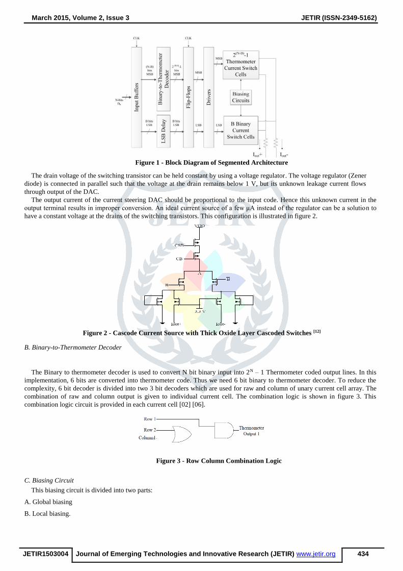
IV. DAC BUILDING BLOCKS
Figure 1 shows the block diagram for the ―(N-B)(MSB) + B(LSB)‖ segmentation. The digital inputs are first clocked into input
registers. Then the first (N-B)/2 MSB’s are column decoded, the next (N-B)/2 bits are row decoded, and the final B bits are
sent to the decoding logic for the Bbit LSB section.
The LSB section is implemented by binary weighted current cells. The main building blocks in this prototype are the unit
current cells, the biasing for the current cells and the thermometer decoder design.
A. Unit Current Cell
The current cell configuration used here is a thick oxide layer transistor for the switch cascode [12].
March 2015, Volume 2, Issue 3 JETIR (ISSN-2349-5162)
JETIR1503004 Journal of Emerging Technologies and Innovative Research (JETIR) www.jetir.org 434
Figure 1 - Block Diagram of Segmented Architecture
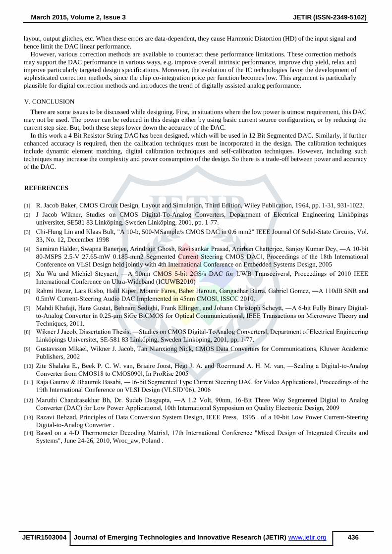
The drain voltage of the switching transistor can be held constant by using a voltage regulator. The voltage regulator (Zener
diode) is connected in parallel such that the voltage at the drain remains below 1 V, but its unknown leakage current flows
through output of the DAC.
The output current of the current steering DAC should be proportional to the input code. Hence this unknown current in the
output terminal results in improper conversion. An ideal current source of a few μA instead of the regulator can be a solution to
have a constant voltage at the drains of the switching transistors. This configuration is illustrated in figure 2.
Figure 2 - Cascode Current Source with Thick Oxide Layer Cascoded Switches [12]
B. Binary-to-Thermometer Decoder
The Binary to thermometer decoder is used to convert N bit binary input into 2N – 1 Thermometer coded output lines. In this
implementation, 6 bits are converted into thermometer code. Thus we need 6 bit binary to thermometer decoder. To reduce the
complexity, 6 bit decoder is divided into two 3 bit decoders which are used for raw and column of unary current cell array. The
combination of raw and column output is given to individual current cell. The combination logic is shown in figure 3. This
combination logic circuit is provided in each current cell [02] [06].
Figure 3 - Row Column Combination Logic
C. Biasing Circuit
This biasing circuit is divided into two parts:
A. Global biasing
B. Local biasing.

March 2015, Volume 2, Issue 3 JETIR (ISSN-2349-5162)
JETIR1503004 Journal of Emerging Technologies and Innovative Research (JETIR) www.jetir.org 435
As shown in figure 4, the global biasing is used to bias the local biasing. The global biasing is provided outside the
current source array, while the local biasing is provided in all current sources. Using global and local biasing avoids problems
with voltage drops across the different interconnects used in the array. The resistor R used in this circuit is off-chip.
Figure 4 - Cascoded Current Mirror based Biasing Circuit [8]
V. PROPOSED DESIGN
FOUR BIT RESISTOR STRING DAC
The major part of design for this resistor string architecture can be categorized as Digital Circuitry (Binary Decoder) and the
resistor string part and the switches to pass the voltages at different nodes to the output. Major problems for this architecture
observed by simulated result are:
1. Glitches
2. Non Linearity
3. Offset
4. Longer Settling time
Figure 4 Schematic of 4 Bit resistor string DAC
Figure 5: Simulation result for Figure 4
The input for this simulation is monotonically increasing 4 bit binary sequence with every step having a width of 25ns. The
two shortcomings glitches and nonlinearity are observable. The glitches have two main reasons first is asynchronous control
signal by digital control circuit. The arrival of unwanted switching signal at the time of transition causes glitching and the
other reason is the voltage difference between the input and output node at the time of transition due to single transistor
switch. Then second one is nonlinearity that is mainly due to the mismatch between the resistors. In this particular
architecture we always have 2N-1 number of switches connected to output that causes a larger parasitic capacitance at output
node and hence also charge accumulation. That’s why we get an offset over their at output and also the response is slower.
VI. CHALLENGES AND FUTURE ENHANCEMENTS
Modern DACs only partially benefit from the recent developments of the CMOS IC processes. While their speeds, e.g.
sampling rates and utilized signal bandwidth, are expected to continue rising, their accuracy, occupied silicon area and
production costs are expected to remain problematic design bottlenecks.
In current steering DACs, the transistor mismatch limits the accuracy of the signal and bias current sources. These tolerances
translate to mismatch among the parallel current cells, causing DAC static and dynamic non-linearity. For good transistor
matching, the transistors need to be made big and laid out close to each other. Other performance limitations include clock-
feedthrough, data-feedthrough, data-dependent disturbances of the substrate and power rails, systematic parasitic due to the
March 2015, Volume 2, Issue 3 JETIR (ISSN-2349-5162)
JETIR1503004 Journal of Emerging Technologies and Innovative Research (JETIR) www.jetir.org 436
layout, output glitches, etc. When these errors are data-dependent, they cause Harmonic Distortion (HD) of the input signal and
hence limit the DAC linear performance.
However, various correction methods are available to counteract these performance limitations. These correction methods
may support the DAC performance in various ways, e.g. improve overall intrinsic performance, improve chip yield, relax and
improve particularly targeted design specifications. Moreover, the evolution of the IC technologies favor the development of
sophisticated correction methods, since the chip co-integration price per function becomes low. This argument is particularly
plausible for digital correction methods and introduces the trend of digitally assisted analog performance.
V. CONCLUSION
There are some issues to be discussed while designing. First, in situations where the low power is utmost requirement, this DAC
may not be used. The power can be reduced in this design either by using basic current source configuration, or by reducing the
current step size. But, both these steps lower down the accuracy of the DAC.
In this work a 4 Bit Resistor String DAC has been designed, which will be used in 12 Bit Segmented DAC. Similarly, if further
enhanced accuracy is required, then the calibration techniques must be incorporated in the design. The calibration techniques
include dynamic element matching, digital calibration techniques and self-calibration techniques. However, including such
techniques may increase the complexity and power consumption of the design. So there is a trade-off between power and accuracy
of the DAC.
REFERENCES
[1] R. Jacob Baker, CMOS Circuit Design, Layout and Simulation, Third Edition, Wiley Publication, 1964, pp. 1-31, 931-1022.
[2] J Jacob Wikner, Studies on CMOS Digital-To-Analog Converters, Department of Electrical Engineering Linköpings
universitet, SE581 83 Linköping, Sweden Linköping, 2001, pp. 1-77.
[3] Chi-Hung Lin and Klaas Bult, "A 10-b, 500-MSample/s CMOS DAC in 0.6 mm2" IEEE Journal Of Solid-State Circuits, Vol.
33, No. 12, December 1998
[4] Samiran Halder, Swapna Banerjee, Arindrajit Ghosh, Ravi sankar Prasad, Anirban Chatterjee, Sanjoy Kumar Dey, ―A 10-bit
80-MSPS 2.5-V 27.65-mW 0.185-mm2 Segmented Current Steering CMOS DAC‖, Proceedings of the 18th International
Conference on VLSI Design held jointly with 4th International Conference on Embedded Systems Design, 2005
[5] Xu Wu and Michiel Steyaert, ―A 90nm CMOS 5-bit 2GS/s DAC for UWB Transceivers‖, Proceedings of 2010 IEEE
International Conference on Ultra-Wideband (ICUWB2010)
[6] Rahmi Hezar, Lars Risbo, Halil Kiper, Mounir Fares, Baher Haroun, Gangadhar Burra, Gabriel Gomez, ―A 110dB SNR and
0.5mW Current-Steering Audio DAC Implemented in 45nm CMOS‖, ISSCC 2010.
[7] Mahdi Khafaji, Hans Gustat, Behnam Sedighi, Frank Ellinger, and Johann Christoph Scheytt, ―A 6-bit Fully Binary Digital-
to-Analog Converter in 0.25-μm SiGe BiCMOS for Optical Communications‖, IEEE Transactions on Microwave Theory and
Techniques, 2011.
[8] Wikner J Jacob, Dissertation Thesis, ―Studies on CMOS Digital-ToAnalog Converters‖, Department of Electrical Engineering
Linköpings Universitet, SE-581 83 Linköping, Sweden Linköping, 2001, pp. 1-77.
[9] Gustavsson Mikael, Wikner J. Jacob, Tan Nianxiong Nick, CMOS Data Converters for Communications, Kluwer Academic
Publishers, 2002
[10] Zite Shalaka E., Beek P. C. W. van, Briaire Joost, Hegt J. A. and Roermund A. H. M. van, ―Scaling a Digital-to-Analog
Converter from CMOS18 to CMOS090‖, In ProRisc 2005
[11] Raja Gaurav & Bhaumik Basabi, ―16-bit Segmented Type Current Steering DAC for Video Applications‖, Proceedings of the
19th International Conference on VLSI Design (VLSID’06), 2006
[12] Maruthi Chandrasekhar Bh, Dr. Sudeb Dasgupta, ―A 1.2 Volt, 90nm, 16-Bit Three Way Segmented Digital to Analog
Converter (DAC) for Low Power Applications‖, 10th International Symposium on Quality Electronic Design, 2009
[13] Razavi Behzad, Principles of Data Conversion System Design, IEEE Press, 1995 . of a 10-bit Low Power Current-Steering
Digital-to-Analog Converter .
[14] Based on a 4-D Thermometer Decoding Matrix‖, 17th International Conference "Mixed Design of Integrated Circuits and
Systems", June 24-26, 2010, Wroc_aw, Poland .