high-speed current-steering digital-to-analog converters
TRANSCRIPT

»ñø;.
é.é@~X
ÿ¡Z
>éøS0Póvf»ð
High-Speed Current-Steering Digital-to-AnalogConverters
@~ß : *¼0>0 : Ò+/
ºÓ»×¾O0`
>éøS0Póvf»ð
High-Speed Current-Steering Digital-to-AnalogConverters
@~ß : * Student : Wei-Hsin Tseng¼0>0 : Ò+/ Advisor : Jieh-Tsorng Wu
»ñø;.
é^.o é. é@~X
ÿ¡Z
A DissertationSubmitted to Department of Electronics Engineering
and Institute of ElectronicsCollege of Electrical and Computer Engineering
National Chiao-Tung Universityin partial Fulfillment of the Requirements
for the Degree ofDoctor of Philosophy
inElectronics Engineering
June 2011Hsin-Chu, Taiwan, Republic of China
ºÓ»×¾O0`

>éøS0Póvf»ð
.ß : * ¼0>0 : Ò+/
»ñø;.
é^.o é. é@~X
`
;GÙ9óÝ£GÎ3óV§¬Î9°£Gs Õ+²
`m»ÕvfÝVãµ®FXáóvf»ð Cvfó
»ð ÎÙÄ6Ý s9°»ð Î=#`²?ûÝn"Bð§
×Ý;GÙÝ>Þã.h´VPÝ»ð Îbú¦mO
Ý
Í¡ZÞ½¥3óvf»ð (Digital-to-Analog Converters, DACs)î¾
>E®éøS0PÚxν2àÝ.Í>§×μyíÐ&é
/I.hb¿y>E®Q&§Ýéø6ð§×ÝPÓ÷VP
(spurious-free dynamic range, SFDR)Ý´íáó*r¾`PÓ÷
VPô¦>ìª Ý1¹?ÝPÓ÷VPh¡Zè5óP
Bóhë° (Digital Random Return-to-Zero, DRRZ)6
Ý@Í¡ZèÝ5óPBóhë°6Ìß@¨×Íâ-NJè
0Íãøóvf»ð ¸àÜè!P[éþhó
vf»ð <®íá`ÍPÓ÷VP8y0è5àíá
¾°F0>+v8y"è"5àÕíᣠâ>+£
i

ÜèmÝ
ÝéøS0Póvf»ð ÎÄ6`éøÙµÿ<g
©PÍÝÇ «ã«SRÝͲéÓ÷éô.
0l´ìª;h¨éÝH5 ¸à´«ÝéøÙQ«éø
ÙÞSR¥Ý<gÍ¡Zè×ÍeÿlÑ*¼1@Þã
ßÍ¡ZèÝeÿlѧ¡Ìß@¨×ÍèÞ-óvf»ð
¸àÜè[éþvéøÙ«©b§¡ÂÝ°y5×hó
vf»ð £ ×yÞèâmÝb[« ××y¶Úy"è
E®>¾NJèÞF"Íãø£¾">+`hóvf
»ð b8yÚè5PÓ÷VP
ii
High-Speed Current-Steering Digital-to-AnalogConverters
Student : Wei-Hsin Tseng Advisor : Jieh-Tsorng Wu
Department of Electronics Engineering
and Institute of Electronics
National Chiao-Tung University
Abstract
In communication systems, most of the information processing is performed in the
digital domain, but the signal carrying the information must be transmitted using analog
signals. Therefore, the use of digital-to-analog(DA) and analog-to-digital(AD) converters
are unavoidable. Data converters are critical for connecting signals to the real world,
often limiting the accuracy and speed of the overall system. As a result, wide-band high-
dynamic-range converters are in high demand.
This thesis focuses on the Digital-to-Analog Converters (DACs). The current-steering
structure has been widely used in high-speed DACs, since in this structure the main
speed limitation comes from the output node, and high sampling speed is thus easily
achieved. However, the non-ideal switching limits the bandwidth of spurious-free dy-
namic range(SFDR). The SFDR decreases rapidly with increasing input frequency. There-
fore, Digital Random Return-to-Zero(DRRZ) is proposed for the high sampling rate current-
steering DAC to maintain high SFDR at high frequency.
iii
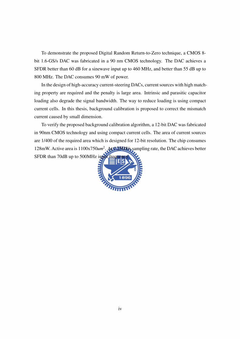
To demonstrate the proposed Digital Random Return-to-Zero technique, a CMOS 8-
bit 1.6-GS/s DAC was fabricated in a 90 nm CMOS technology. The DAC achieves a
SFDR better than 60 dB for a sinewave input up to 460 MHz, and better than 55 dB up to
800 MHz. The DAC consumes 90 mW of power.
In the design of high-accuracy current-steering DACs, current sources with high match-
ing property are required and the penalty is large area. Intrinsic and parasitic capacitor
loading also degrade the signal bandwidth. The way to reduce loading is using compact
current cells. In this thesis, background calibration is proposed to correct the mismatch
current caused by small dimension.
To verify the proposed background calibration algorithm, a 12-bit DAC was fabricated
in 90nm CMOS technology and using compact current cells. The area of current sources
are 1/400 of the required area which is designed for 12-bit resolution. The chip consumes
128mW. Active area is 1100x750um2. At 1.25GS/s sampling rate, the DAC achieves better
SFDR than 70dB up to 500MHz input frequency.
iv

*
´&E&ݼ0>0>Ò+/>0lîtÝݯ3&
ÿ° Íì2&¼0ÜÃ|C@~§FîÝ£[!`ô3/
î.êÕÝ@~ÝVõ§®ÞÝ]°9°Å(K¸&åÇ9¬vÕ
ßp
307@±¼Ý.6øAdoM¡?Ñr
Ço@'KÁH<D¡èøݯ&|5¿Wh¡
Z
307!.|C.rú]¿Òh8ùâÅ"ù
ãO³¬Û?t8å|CÄ6|Æ39¿O@~Ä
Ê`ÝQÃ3hlî05Ý
¨²&æI*CкéÝÜÃèº&%®þnÝ^º¯
&ÿ|Þ&Ýx; @jÝW`
h²&©½&ÝY|C&Ýß. ¯ÆÝ9OY¹
<¸Ý&bæW9@~3h=T2Æ
*
»ñø;.
ºÓ»×¾O0`
v

vi
Contents
Z` i
English Abstract iii
* v
List of Tables ix
List of Figures xi
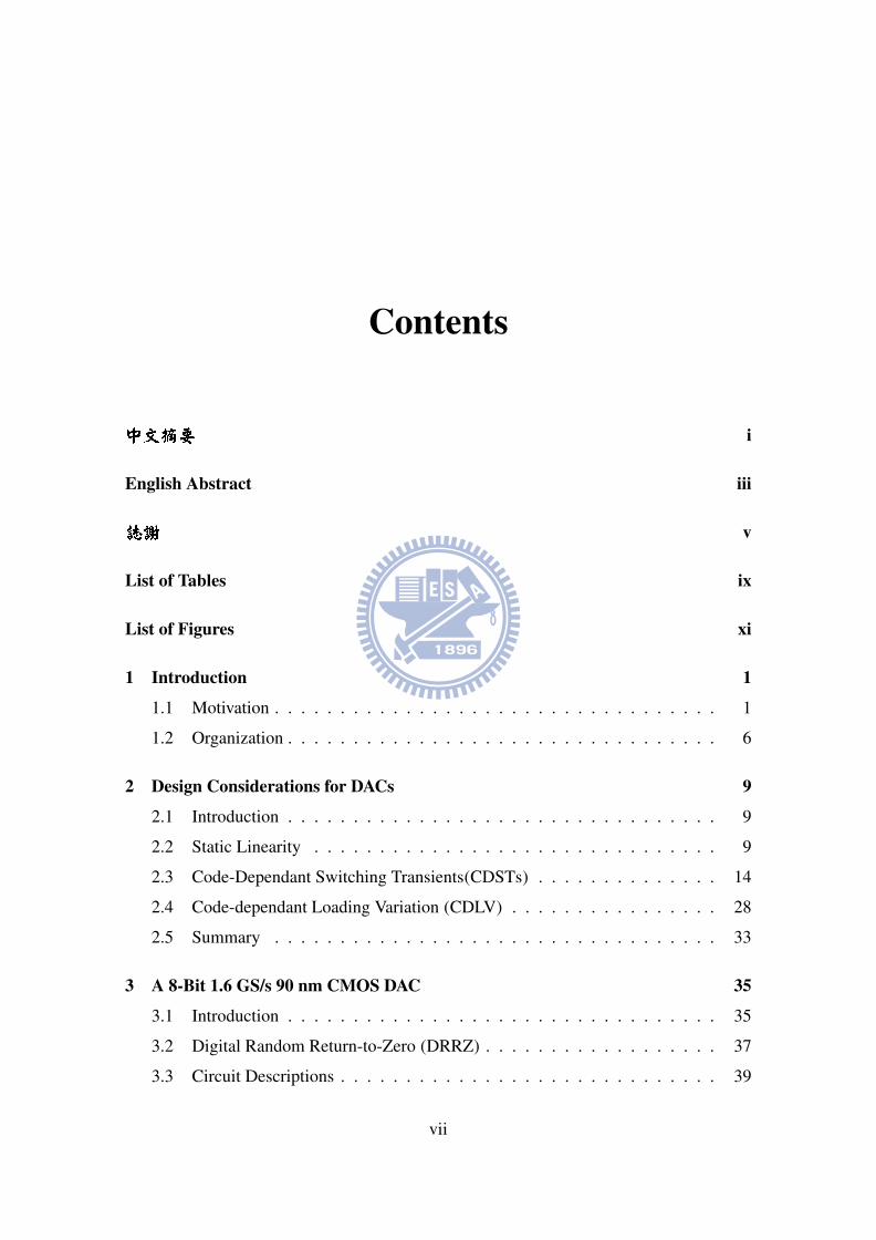
1 Introduction 1
1.1 Motivation . . . . . . . . . . . . . . . . . . . . . . . . . . . . . . . . . . 1
1.2 Organization . . . . . . . . . . . . . . . . . . . . . . . . . . . . . . . . . 6
2 Design Considerations for DACs 9
2.1 Introduction . . . . . . . . . . . . . . . . . . . . . . . . . . . . . . . . . 9
2.2 Static Linearity . . . . . . . . . . . . . . . . . . . . . . . . . . . . . . . 9
2.3 Code-Dependant Switching Transients(CDSTs) . . . . . . . . . . . . . . 14
2.4 Code-dependant Loading Variation (CDLV) . . . . . . . . . . . . . . . . 28
2.5 Summary . . . . . . . . . . . . . . . . . . . . . . . . . . . . . . . . . . 33
3 A 8-Bit 1.6 GS/s 90 nm CMOS DAC 35
3.1 Introduction . . . . . . . . . . . . . . . . . . . . . . . . . . . . . . . . . 35
3.2 Digital Random Return-to-Zero (DRRZ) . . . . . . . . . . . . . . . . . . 37
3.3 Circuit Descriptions . . . . . . . . . . . . . . . . . . . . . . . . . . . . . 39
vii
3.4 Experimental Results . . . . . . . . . . . . . . . . . . . . . . . . . . . . 43
3.5 Summary . . . . . . . . . . . . . . . . . . . . . . . . . . . . . . . . . . 53
4 A 12-Bit 1.25-GS/s Background Calibrated DAC 55
4.1 Introduction . . . . . . . . . . . . . . . . . . . . . . . . . . . . . . . . . 55
4.2 Design for High Signal Bandwidth . . . . . . . . . . . . . . . . . . . . . 57
4.3 DAC Architecture . . . . . . . . . . . . . . . . . . . . . . . . . . . . . . 60
4.4 Current-Cell Background Calibration . . . . . . . . . . . . . . . . . . . . 65
4.5 Experimental Results . . . . . . . . . . . . . . . . . . . . . . . . . . . . 77
4.6 Summary . . . . . . . . . . . . . . . . . . . . . . . . . . . . . . . . . . 90
5 Conclusions and Future Works 93
5.1 Conclusions . . . . . . . . . . . . . . . . . . . . . . . . . . . . . . . . . 93
5.2 Recommendations for Future Investigation . . . . . . . . . . . . . . . . . 94
Bibliography 95
F 101
Publication List 102
viii

List of Tables
2.1 Maximum INL of a 8-bit 5-3 segment DAC . . . . . . . . . . . . . . . . 12
2.2 The required area versus different gate overdrive . . . . . . . . . . . . . . 12
2.3 The relationship between yield and sigma . . . . . . . . . . . . . . . . . 12
2.4 Different segmentations for —HD3—=70dB . . . . . . . . . . . . . . . 30
3.1 DAC Performance Summary . . . . . . . . . . . . . . . . . . . . . . . . 51
4.1 Dimensions of MOSFETs in the M-DAC . . . . . . . . . . . . . . . . . . 63
4.2 DAC specifications . . . . . . . . . . . . . . . . . . . . . . . . . . . . . 89
4.3 Comparison of Published High-Speed DACs. . . . . . . . . . . . . . . . 90
ix

x

List of Figures
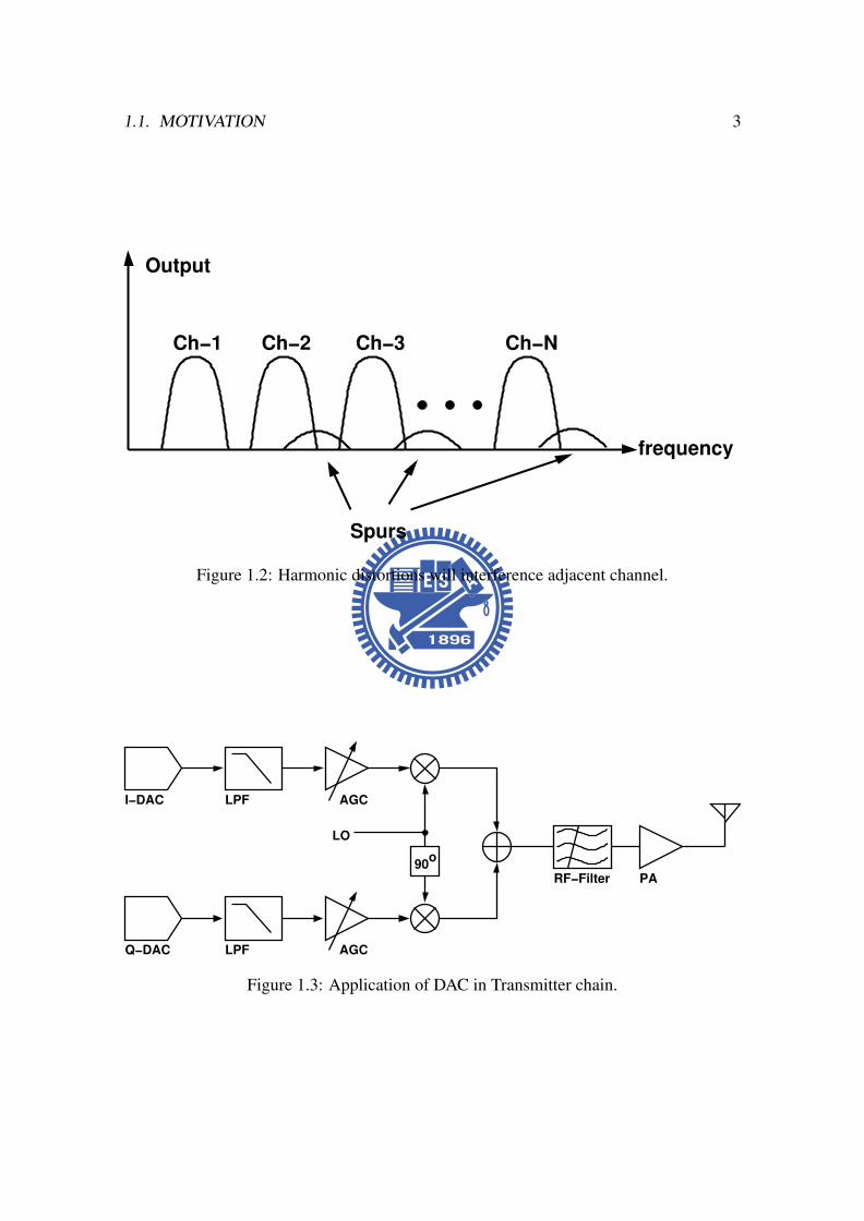
1.1 Block diagram of multi channel transmitter for cable modem. . . . . . . . 2
1.2 Harmonic distortions will interference adjacent channel. . . . . . . . . . 3
1.3 Application of DAC in Transmitter chain. . . . . . . . . . . . . . . . . . 3
1.4 The ARZ can be expressed as an equivalent switch at output node. . . . . 4
1.5 Code-dependent loading variation (CDLV). . . . . . . . . . . . . . . . . 5
2.1 A DAC with worse DNL and INL . . . . . . . . . . . . . . . . . . . . . 10
2.2 When the INL is as large as 10LSB in Figure 2.1, the spectrum is spurious
with odd and even order harmonic distortions. . . . . . . . . . . . . . . . 11
2.3 A 3-bit 3-layer DEM DAC . . . . . . . . . . . . . . . . . . . . . . . . . 13
2.4 Calibrated DAC architecture proposed by Cong . . . . . . . . . . . . . . 15
2.5 Calibrated DAC architecture proposed by Q. Huang . . . . . . . . . . . . 15
2.6 Code-dependent switching transient (CDST). . . . . . . . . . . . . . . . 16
2.7 Unit current cell with ideal current source, resistor and latch driver. The
current switches are thick oxide device. . . . . . . . . . . . . . . . . . . 18
2.8 Simulated Spectrum with sample rate 1GS/s switches size W=2.44um
L=0.24um and SFDR 52.5dB. . . . . . . . . . . . . . . . . . . . . . . . 19
2.9 Simulated Spectrum with sample rate 1GS/s switches size W=1.44um
L=0.24um and SFDR 55.3dB. . . . . . . . . . . . . . . . . . . . . . . . 20
2.10 Simulated Spectrum with sample rate 200MS/s switches size W=2.44um
L=0.24um and SFDR 64.7dB. . . . . . . . . . . . . . . . . . . . . . . . 21
2.11 SFDR summary of different switch sizes and sampling rates. . . . . . . . 22
2.12 3 cells out of 63 with 10ps clk skew. . . . . . . . . . . . . . . . . . . . . 24
xi

2.13 3 cells out of 63 with 10ps clk skew. . . . . . . . . . . . . . . . . . . . . 25
2.14 Spectra of the DAC’s output signal. 6-6 segmentation only one latch with
weak driving strength of 80ps of rising/falling time and others with 50ps. 26
2.15 The latch’s differential output cross-point dominate the voltage fluctuation
of the internal node. . . . . . . . . . . . . . . . . . . . . . . . . . . . . . 27
2.16 Code-dependent loading variation (CDLV). . . . . . . . . . . . . . . . . 27
2.17 Zu is the simulated output impedance of one current cell when one switch
is off. . . . . . . . . . . . . . . . . . . . . . . . . . . . . . . . . . . . . 29
2.18 The frequency response of Zu . . . . . . . . . . . . . . . . . . . . . . . 29
2.19 The required output impedance versus specified SFDR for 12-bit DAC.
The degree of segmentation does not influence the output impedance re-
quirement. . . . . . . . . . . . . . . . . . . . . . . . . . . . . . . . . . . 30
2.20 Output impedance requirement of unit current cell vs. bit number of DAC.
The CDLV caused HD2, HD3 must larger than 70dB and RL is 50ohm. . 31
2.21 Output impedance requirement of unit current cell vs. bit number of DAC.
The single ended INL caused by CDLV must small than 0.5LSB and RL
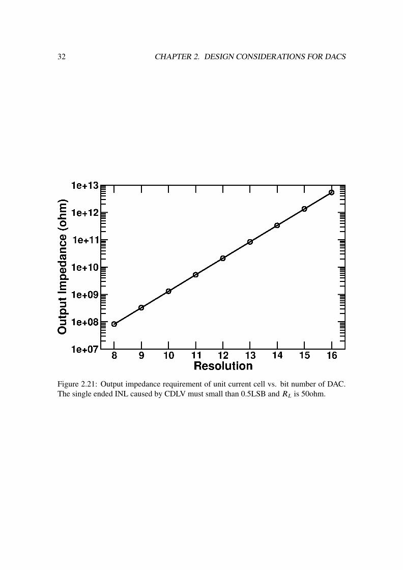
is 50ohm. . . . . . . . . . . . . . . . . . . . . . . . . . . . . . . . . . . 32
3.1 A current-steering DAC. . . . . . . . . . . . . . . . . . . . . . . . . . . 36
3.2 Non-return-to-zero (NRZ) output waveform of a current-steering DAC. . 37
3.3 Waveforms of a return-to-zero (RZ) DAC. . . . . . . . . . . . . . . . . . 37
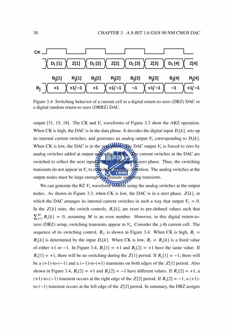
3.4 Switching behavior of a current cell in a digital return-to-zero (DRZ)
DAC or a digital random return-to-zero (DRRZ) DAC. . . . . . . . . . . 38
3.5 DAC block diagram. . . . . . . . . . . . . . . . . . . . . . . . . . . . . 40
3.6 Current cell schematic. . . . . . . . . . . . . . . . . . . . . . . . . . . . 42
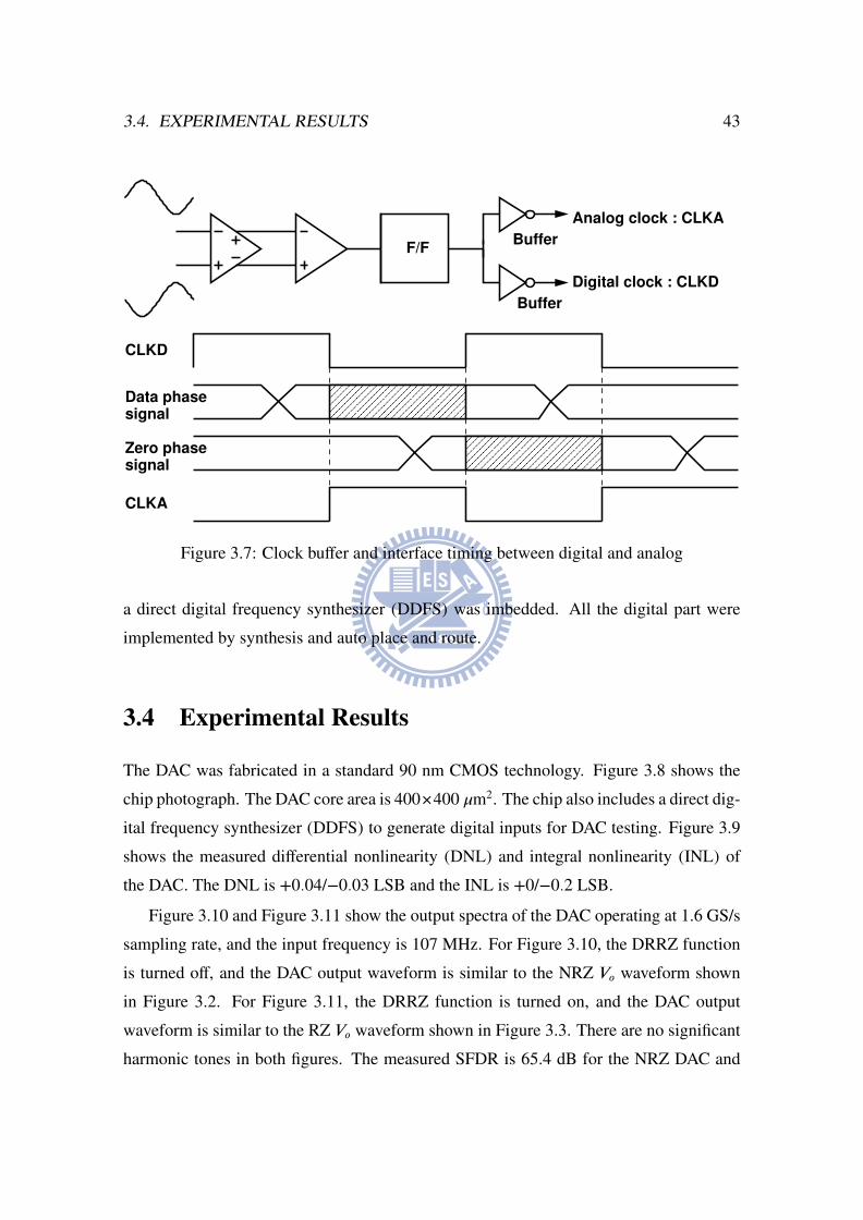
3.7 Clock buffer and interface timing between digital and analog . . . . . . . 43
3.8 Microphotograph of the DRRZ DAC . . . . . . . . . . . . . . . . . . . . 44
3.9 Measured differential nonlinearity (DNL) and integral nonlinearity (INL). 45
3.10 Output spectrum of the DAC with NRZ. Sampling rate is 1.6 GS/s, input
frequency is 107 MHz. . . . . . . . . . . . . . . . . . . . . . . . . . . . 46
xii
3.11 Output spectrum of the DAC with DRRZ. Sampling rate is 1.6 GS/s, input
frequency is 107 MHz. . . . . . . . . . . . . . . . . . . . . . . . . . . . 47
3.12 Output spectrum of the DAC with NRZ. Sampling rate is 1.6 GS/s, input
frequency is 731 MHz. . . . . . . . . . . . . . . . . . . . . . . . . . . . 48
3.13 Output spectrum of the DAC with DRRZ. Sampling rate is 1.6 GS/s, input
frequency is 731 MHz. . . . . . . . . . . . . . . . . . . . . . . . . . . . 49
3.14 Measured SFDR at different signal frequencies. . . . . . . . . . . . . . . 50
3.15 Dynamic performance comparison of published DACs. . . . . . . . . . . 52
4.1 A current-steering DAC. . . . . . . . . . . . . . . . . . . . . . . . . . . 56
4.2 Code-dependent switching transient (CDST). . . . . . . . . . . . . . . . 58
4.3 Code-dependent loading variation (CDLV). . . . . . . . . . . . . . . . . 59
4.4 A segmented 12-bit DAC. . . . . . . . . . . . . . . . . . . . . . . . . . . 61
4.5 Pseudo random number generator (PRNG). . . . . . . . . . . . . . . . . 62
4.6 Schematic of the j-th M-DAC current cell. . . . . . . . . . . . . . . . . . 64
4.7 Zero-phase current-mismatch modulation . . . . . . . . . . . . . . . . . 66
4.8 Zero-phase current-mismatch modulation . . . . . . . . . . . . . . . . . 67
4.9 DAC block diagram. . . . . . . . . . . . . . . . . . . . . . . . . . . . . 68
4.10 Various waveforms in calibration signal path. . . . . . . . . . . . . . . . 69
4.11 The C-DAC and BUS master. . . . . . . . . . . . . . . . . . . . . . . . . 70
4.12 The C-DAC and transfer function. . . . . . . . . . . . . . . . . . . . . . 71
4.13 Dm-to-Da mapping function. . . . . . . . . . . . . . . . . . . . . . . . . 72
4.14 Schematic of the calibration analog signal path. . . . . . . . . . . . . . . 73
4.15 Mismatch information loss due to the finite output port bandwidth . . . . 75
4.16 Calibration cycle vs. output port bandwidth . . . . . . . . . . . . . . . . 77
4.17 Microphotograph of the DAC. . . . . . . . . . . . . . . . . . . . . . . . 78
4.18 Measured DNL and INL before current-cell calibration. . . . . . . . . . . 80
4.19 Measured DNL and INL after current-cell calibration. . . . . . . . . . . . 80
4.20 Measured DAC full-scale transient response. . . . . . . . . . . . . . . . . 81
4.21 Measured DAC output spectrum without calibration and DRRZ. Sampling
rate is 1.25 GS/s. Input frequency is 40 MHz. . . . . . . . . . . . . . . . 82
xiii

4.22 Measured DAC output spectrum after calibration but without DRRZ. Sam-
pling rate is 1.25 GS/s. Input frequency is 40 MHz. . . . . . . . . . . . . 83
4.23 Measured DAC output spectrum after calibration but without DRRZ. Sam-
pling rate is 1.25 GS/s. Input frequency is 477 MHz. . . . . . . . . . . . 84
4.24 Measured DAC output spectrum after calibration and with DRRZ. Sam-
pling rate is 1.25 GS/s. Input frequency is 477 MHz. . . . . . . . . . . . 85
4.26 Measured SFDR versus input frequencies . . . . . . . . . . . . . . . . . 87
4.27 Measured SNDR versus input frequencies. The SNDR of the DAC is
limited by the Signal Analyzer . . . . . . . . . . . . . . . . . . . . . . . 88
4.28 SFDR performance comparison. . . . . . . . . . . . . . . . . . . . . . . 89
xiv
Chapter 1
Introduction
1.1 Motivation
In communication systems, most of the information processing is performed in the digital
domain, but the signal carrying the information must be transmitted using analog signals.
Therefore, the use of digital-to-analog(DA) and analog-to-digital(AD) converters are un-
avoidable. Data converters are critical for connecting signals to the real world, often
limiting the accuracy and speed of the overall system and this work focuses on the DACs.
Wide-band high-dynamic-range DACs are in high demand, especially for multicarrier ra-
dio applications [1, 2]. A simplified architecture of a cable modem head end transmitter is
shown in Figure 1.1. The cable modem system consists of multiple channels, where each
channel contains a digital modulator and a DAC. When multiple channels are combined
simultaneously, as shown in Figure 1.2, the SFDR of the DAC should meet a minimum
SFDR. If the SFDR is worse than the requirement,signals in one channel will be corrupted
by spurious components from other channels. Therefore, the major challenge for design-
ing DAC of frequency domain applications is to obtain a wide-band SFDR. Moreover,
if the DAC can provide a high sampling rate and large SFDR bandwidth, the multiple
channel signal can be combined in digital domain. Then, the digital code can be delivered
by one DAC. Figure 1.3 [3] shows another example, a signal transmission over radio fre-
quency (RF) involves a complex system design. A baseband message, typically digital, is
converted to an analog signal through a DAC at the beginning of the transmission system
1

2 CHAPTER 1. INTRODUCTION
Modulator
Modulator
ModulatorChannel_1
Channel_2
Channel_N
DAC Output
Figure 1.1: Block diagram of multi channel transmitter for cable modem.
and a series of analog processing which filtering the signal suitable for RF transmission.
If the DACs are designed with good high frequency SFDR, the requirement of filter can
be relaxed [4].
In recent years, many arts have been published on high-speed DAC design [1, 5, 6, 7,
8, 4, 9, 10, 11, 12]. Most of these designs concentrate on obtaining good low-frequency
performance, but they do not perform well at higher frequencies. In [9], the spectrum
shows that spurs, almost harmonic distortions, can be improved because they are higher
than the noise floor. Therefore, the goal of this work is to reduce the harmonic distor-
tions at high and low frequency. We should know the key points that cause harmonic
distortions. At low frequency, the performance is limited by static linearity, DNL and
INL, the nonlinearity source is from mismatch of current cells. To design a DAC, de-
signers take care of matching by matching properties of MOSFET [13] or use techniques
such as calibration [14, 15, 16, 17, 5, 18, 19, 20, 21, 22, 23], dynamic element matching
[24, 25, 26, 27, 28], and random walks [29, 30]. That is, several ways can be used to have
a good static linearity.
In [17], the measured DNL and INL are good, but SFDR still drops at high frequen-
cies. The reason is that the DACs cause more switching transients. Switching transient
is the non-ideal temporary waveform at output node when switching occurs. Each cur-
1.1. MOTIVATION 3
frequency
Output
Ch−1 Ch−3
Spurs
Ch−NCh−2
Figure 1.2: Harmonic distortions will interference adjacent channel.
90o
LPF AGC
LPF AGC
Q−DAC
LO
I−DAC
PARF−Filter
Figure 1.3: Application of DAC in Transmitter chain.

4 CHAPTER 1. INTRODUCTION
Di Di Di Di
Vo
Iu
jB
Di Vo1 Vo2
RZ
[1] [2] [3] [4]
[k]
Dec
oder
[k]
CK
t
RZ
Latc
h
CK
M
Figure 1.4: The ARZ can be expressed as an equivalent switch at output node.

1.1. MOTIVATION 5
rent cell has different switching transients due to clock skew, drivers mismatch, signal
feed-through, and internal node fluctuation. In other words, they are cell dependant, also
called code-dependant, and will result in harmonic distortions. This is why the prior arts
perform well at low frequencies but not well at high frequencies. In [31], analog return-
to-zero(ARZ) was proposed to mitigate this effect. As shown in Figure 1.4, ARZ can be
expressed as an equivalent switch at output node and controlled by the signal RZ. The RZ
signal has a phase delay with clock. When RZ is low, the switch will short the output and
force the differential current to zero. If switching transient occurs at this state, they would
be hidden by the switch. However, the switch is on the signal path, the turn-on resistor
must be small for good linearity. Most of high speed DACs output 16 mA of current. It
means that the switch will pass 8mA, the area cost of this switch is very high and induce
parasitic capacitor, which is a serious disadvantage for high sampling rate.
In this thesis, we proposed a digital return-to-zero (DRZ). It can be realized by only
replacing the latch architecture and digital input sequence. Moreover, random sequence
is inserted into the digital return-to-zero. Then, the switch transients are randomized into
noise floor, and SFDR will be improved. This new technique is digital random return-to-
zero, called DRRZ. A lower resolution, 8-bit, DACs was fabricated in 90nm COMS to
verify the DRRZ [32], and the sampling rate is 1.6GS/s.
Iu
Vo1 Vo2
LRLR
IuuR Cu
Vo1 Vo2
LR LR
Vo1 Vo2
LR LR
Co1o1R o2RCo2 Io2Io1
Figure 1.5: Code-dependent loading variation (CDLV).
Figure 1.5 shows another source of harmonic distortion. Each current cell is modeled
as an ideal switch on top of an ideal current source Iu in parallel with a resistor Ru and
a capacitor Cu. The resistor Ru represents the output resistance of the current source.
6 CHAPTER 1. INTRODUCTION
The capacitor Cu represents the capacitance associated with the output node of the current
source, including the gate capacitance of the current switch. Both Ru and Cu are con-
nected to either the Vo1 node or the Vo2 node, depending on the state of the switch. As a
result, the total loadings for output nodes Vo1 and Vo2 vary with digital input Di[k]. This
code-dependent loading variation (CDLV) effect introduces harmonic distortion in the
differential output Vo = Vo1 − Vo2. Increasing Ru and reducing Cu can mitigate the CDLV
effect. Adding cascode stage to a current source can increase Ru. In most designs, the
CDLV effect at high frequencies is dominated by Cu. The Cu capacitance is determined
by the device dimensions of the current switch and the current source, while the device di-
mensions are governed by the matching requirements. The CDLV effect can be mitigated
by adding an additional cascode stage following the current switch in each current cell
[33, 7, 34]. The MOSFETs in those cascode stages need to have large transconductances
to achieve good high-frequency performance [34, 12].
For this work, instead of adding additional cascode stages, we simply use smaller
devices for both the current sources and the current switches to reduceCu. Smaller devices
lead to larger mismatches. However, due to the use of DRRZ, the matching requirement
for the current switches is relaxed. We also propose a new calibration algorithm for the
using of smaller current cells which will reduce parasitic capacitor; therefore, the DACs
would be operated in higher sampling rate. A 12-bit 1.25GS/s DAC[35] is implemented
as a design example.
1.2 Organization
The organization of the thesis is described as follows:
Chapter 2 discusses the highlight to design a high speed high performance current-
steering DACs. Including transient effect, finite output impedance effect and static linear-
ity. And introduce the techniques to improve the static and dynamic performances.
Chapter 3 describes a 8-bit and with a high sampling rate of 1.6GS/s DAC. This DAC
is designed to demonstrate the digital random return-to-zero(DRRZ) can improve the high
output frequency SFDR.
In Chapter 4, base on the DRRZ technique, we develop a background calibration

1.2. ORGANIZATION 7
technique to overcome the mismatch due to small size. Since small size is used for high
speed and wide SFDR bandwidth.
Finally, conclusions and recommendations for future works will be given in Chapter 5.

8 CHAPTER 1. INTRODUCTION
Chapter 2
Design Considerations for DACs
2.1 Introduction
This chapter lists three sections for designing a high performance of current-steering DAC.
The first is basic resolution requirement or static linearity. In general design, the matching
is guaranteed by large size and gate over-drive voltage. The second and the third are code-
dependant switching transient (CDST) and code-dependant loading variation(CDLV) re-
spectively. The static linearity impacts the both signal to noise ratio (SNR) and SFDR.
The effects of CDST and CDLV will result in the degradation of SFDR.
2.2 Static Linearity
The DAC static linearity is specified as differential nonlinearity (DNL) and integral non-
linearity (INL). In the design of high-accuracy current steering DACs, the matching prop-
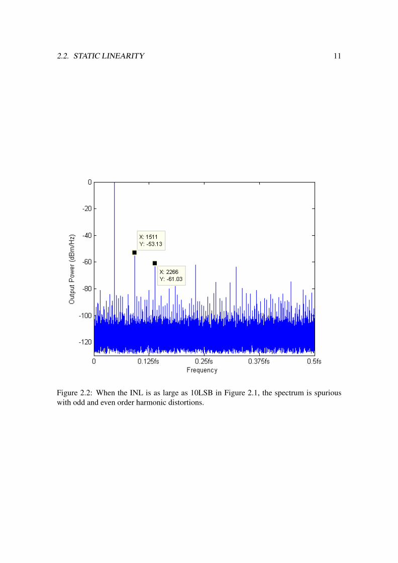
erties are the first issue that should be concerned. For example, the DNL and INL of a
DAC are shown in Figure 2.1. While the INL is as large as 10LSBs, the spectrum shown
in Figure 2.2 is spurious with odd and even order harmonic distortions. As a result, the
dynamic performance of a current-steering DAC is limited by not only frequency but also
static linearity. This section will discuss the technique for good static linearity.
I. Matching property
In a simple design, we can choose proper device sizes for the matching of transistors
9

10 CHAPTER 2. DESIGN CONSIDERATIONS FOR DACS
Figure 2.1: A DAC with worse DNL and INL
2.2. STATIC LINEARITY 11
Figure 2.2: When the INL is as large as 10LSB in Figure 2.1, the spectrum is spuriouswith odd and even order harmonic distortions.
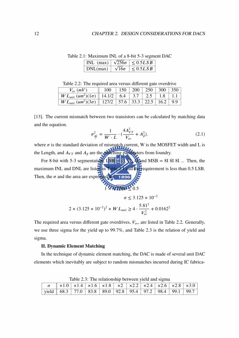
12 CHAPTER 2. DESIGN CONSIDERATIONS FOR DACS
Table 2.1: Maximum INL of a 8-bit 5-3 segment DACINL (max)
√256σ ≤ 0.5LSB
DNL(max)√
16σ ≤ 0.5LSB
Table 2.2: The required area versus different gate overdriveVov (mV ) 100 150 200 250 300 350
WLunit (um2)(1σ) 14.1/2 6.4 3.7 2.5 1.8 1.1WLunit (um2)(3σ) 127/2 57.6 33.3 22.5 16.2 9.9
[13]. The current mismatch between two transistors can be calculated by matching data
and the equation.
σ2∆II
=1
W · L· (
4A2V T
Vov+ A2
β), (2.1)
where σ is the standard deviation of mismatch current, W is the MOSFET width and L is
the Length, and AV T and Aβ are the matching parameters from foundry.
For 8-bit with 5-3 segmentation, LSB = 1I, 2I, 4I and MSB = 8I 8I 8I ... Then, the
maximum INL and DNL are listed in Table 2.1 and the requirement is less than 0.5 LSB.
Then, the σ and the area are expressed as
1 ×√
256σ ≤ 0.5
σ ≤ 3.125 × 10⁻²
2 × (3.125 × 10−2)2 ×WLunit ≥ 4 ·5.812
V 2ov
+ 0.01622
The required area versus different gate overdrives, Vov, are listed in Table 2.2. Generally,
we use three sigma for the yield up to 99.7%, and Table 2.3 is the relation of yield and
sigma.
II. Dynamic Element Matching
In the technique of dynamic element matching, the DAC is made of several unit DAC
elements which inevitably are subject to random mismatches incurred during IC fabrica-
Table 2.3: The relationship between yield and sigmaσ ×1.0 ×1.4 ×1.6 ×1.8 ×2 ×2.2 ×2.4 ×2.6 ×2.8 ×3.0
yield 68.3 77.0 83.8 89.0 92.8 95.4 97.2 98.4 99.1 99.7
2.2. STATIC LINEARITY 13
S 1,2
S 1,1
S 1,4
S 1,3
S 2,1
S 2,2
S 3,1
1−bitDAC
1−bitDAC
1−bitDAC
1−bitDAC
1−bitDAC
1−bitDAC
1−bitDAC
1−bitDAC
x[n] 3
10
1
1
1
1
1
1
1
1
2
2
2
2
3
3
Layer1
Layer2
Layer3
y[n]
b k
b k
b k
b k−1b k−2
b 0 1
11
11
1
R[n]
y [n]
y [n]
y [n]
y [n]
y [n]
y [n]
y [n]
y [n]
1
2
3
4
5
6
7
8
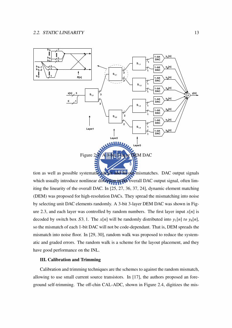
Figure 2.3: A 3-bit 3-layer DEM DAC
tion as well as possible systematic circuit and layout mismatches. DAC output signals
which usually introduce nonlinear distortion in the overall DAC output signal, often lim-
iting the linearity of the overall DAC. In [25, 27, 36, 37, 24], dynamic element matching
(DEM) was proposed for high-resolution DACs. They spread the mismatching into noise
by selecting unit DAC elements randomly. A 3-bit 3-layer DEM DAC was shown in Fig-
ure 2.3, and each layer was controlled by random numbers. The first layer input x[n] is
decoded by switch box S3, 1. The x[n] will be randomly distributed into y1[n] to y8[n],
so the mismatch of each 1-bit DAC will not be code-dependant. That is, DEM spreads the
mismatch into noise floor. In [29, 30], random walk was proposed to reduce the system-
atic and graded errors. The random walk is a scheme for the layout placement, and they
have good performance on the INL.
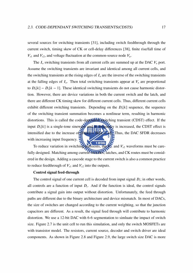
III. Calibration and Trimming
Calibration and trimming techniques are the schemes to against the random mismatch,
allowing to use small current source transistors. In [17], the authors proposed an fore-
ground self-trimming. The off-chin CAL-ADC, shown in Figure 2.4, digitizes the mis-
14 CHAPTER 2. DESIGN CONSIDERATIONS FOR DACS
match of each MSB current cells at star-up step. Then, the mismatch are stored in memory
and a CAL-DAC is used to compensate the total mismatch of the MSB current cells. And
in [5], the authors also proposed an off-line self-trimming technique which is based on
the trimmable floating gate. The gate can be charged and discharged, and then the current
is changed. However, the foreground self-trimming techniques lack of tracking ability of
supply and temperature variation. There would be a 0.7 LSB drift over temperature varia-
tion form -40 to 85 degrees [20]. As a result, the author proposed background calibration
technique which can work under the normal operation. The floating current sources [15]
provide the current from the tail node, so the current calibration does not interrupt the
normal operation. In [18], the floating source and an analog calibration loop are shown in
Figure 2.5. The current comparator locates at right-half side, and the total current of the
current source injects into comparator at node A. The cell current and IB are summed to
be compared with IR. If IR is larger than the total current, the Cstore will be discharged.
During the guard time between two consecutive calibration phases when MSB cells are
switched, the parasitic capacitance at node B may discharge due to the temporary current
imbalance. To prevent subsequent charge-sharing from causing glitches, the latter is sam-
pled by a common tracking capacitor Chold during the phase before the particular MSB
be calibrated. This pre-sampled voltage VHi is then used to hold the voltage on node B
through a buffer during the guard time to make the transition seamless.
2.3 Code-Dependant Switching Transients(CDSTs)
At the beginning of this section, we define and introduce what code-dependant switching
transient is.
Figure 2.6 shows the operation of a single current cell. The current cell contains a
current source Iu and a MOSFET current switch M1-M2. Upon the rising edge of clock
CK, the binary input Bj[k] is loaded into the latch. Its two complementary outputs, Vs1and Vs2, drive the current switch, directing the Iu current to either output node Vo1 or output
node Vo2. Figure 2.6 also shows the transient response of the differential output current
Io = Io1 − Io2. The output current Io is a combination of an ideal transient response
and switching transients. Switching transients occur only when Bj[k] varies. There are
2.3. CODE-DEPENDANT SWITCHING TRANSIENTS(CDSTS) 15
Bias Gen.
Latc
hLa
tch
14−BitDAC
8+2−bitCAL−DAC
Calibration Controller
CAL−ADC
Dec
oder
RAM
Din
VDD
Figure 2.4: Calibrated DAC architecture proposed by Cong
IRIB
Chold
Strim
Cstore
Ssample SpchrgB
A
VHi
VDD
VDD
Figure 2.5: Calibrated DAC architecture proposed by Q. Huang

16 CHAPTER 2. DESIGN CONSIDERATIONS FOR DACS
Io
Io
Io
Vs1
Vs2
Vo1 Vo2
Io1 Io2
Vs1 Vs2Va
Iu
jB
Transient Response
Ideal Transient Response
Switching Transients
[k] t
t
t
CK
Latch
M1 M2
CK
Figure 2.6: Code-dependent switching transient (CDST).
2.3. CODE-DEPENDANT SWITCHING TRANSIENTS(CDSTS) 17
several sources for switching transients [31], including switch feedthrough through the
current switch, timing skew of CK or cell-delay differences [38], finite rise/fall time of
Vs1 and Vs2, and voltage fluctuation at the common-source node Va.
The Io switching transients from all current cells are summed up at the DAC Vo port.
Assume the switching transients are invariant and identical among all current cells, and
the switching transients at the rising edges of Io are the inverse of the switching transients
at the falling edges of Io. Then total switching transients appear at Vo are proportional
to Di[k] −Di[k − 1]. These identical switching transients do not cause harmonic distor-
tion. However, there are device variations in both the current switch and the latch, and
there are different CK timing skew for different current cells. Thus, different current cells
exhibit different switching transients. Depending on the Di[k] sequence, the sequence
of the switching transient summation becomes a nonlinear term, resulting in harmonic
distortions. This is called the code-dependent switching transient (CDST) effect. If the
input Di[k] is a single-tone sinewave and its frequency is increased, the CDST effect is
intensified due to the increase of |Di[k] − Di[k − 1]|. Thus, the DAC SFDR decreases
with increasing input frequency.
To reduce variation in switching transients, the Vs1 and Vs2 waveforms must be care-
fully designed. Matching among current switches, latches, and CK routes must be consid-
ered in the design. Adding a cascode stage to the current switch is also a common practice
to reduce feedthrough of Vs1 and Vs2 into the outputs.
Control signal feed-through
The control signal of one current cell is decoded from input signal Di; in other words,
all controls are a function of input Di. And if the function is ideal, the control signals
contribute a signal gain into output without distortion. Unfortunately, the feed through
paths are different due to the binary architecture and device mismatch. In most of DACs,
the size of switches are changed according to the current weighting, so that the junction
capacitors are different. As a result, the signal feed through will contribute to harmonic
distortion. We use a 12-bit DAC with 6-6 segmentation to simluate the impact of switch
size. Figure 2.7 is the unit cell to run this simulation, and only the switch MOSFETs are
with transistor model. The resistors, current source, decoder and switch driver are ideal
components. As shown in Figure 2.8 and Figure 2.9, the large switch size DAC is more

18 CHAPTER 2. DESIGN CONSIDERATIONS FOR DACS
Vo1 Vo2
Iu : Ideal CS 4uA
R=25ohm
VDD =2.5V
& Latch DriverBehavior Decoder
VDD VDD
Figure 2.7: Unit current cell with ideal current source, resistor and latch driver. Thecurrent switches are thick oxide device.
2.3. CODE-DEPENDANT SWITCHING TRANSIENTS(CDSTS) 19
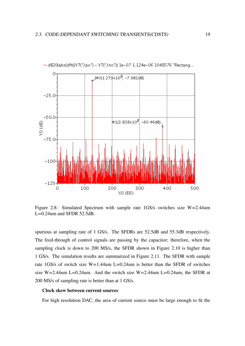
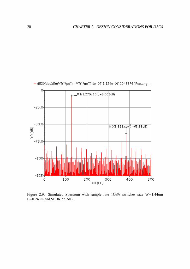
Figure 2.8: Simulated Spectrum with sample rate 1GS/s switches size W=2.44umL=0.24um and SFDR 52.5dB.
spurious at sampling rate of 1 GS/s. The SFDRs are 52.5dB and 55.3dB respectively.
The feed-through of control signals are passing by the capacitor; therefore, when the
sampling clock is down to 200 MS/s, the SFDR shown in Figure 2.10 is higher than
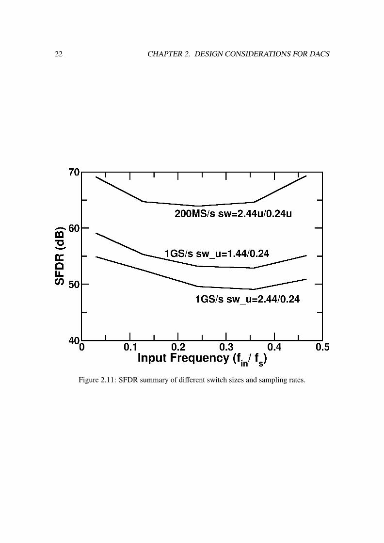
1 GS/s. The simulation results are summarized in Figure 2.11. The SFDR with sample
rate 1GS/s of switch size W=1.44um L=0.24um is better than the SFDR of switches
size W=2.44um L=0.24um. And the switch size W=2.44um L=0.24um, the SFDR at
200 MS/s of sampling rate is better than at 1 GS/s.
Clock skew between current sources
For high resolution DAC, the area of current source must be large enough to fit the
20 CHAPTER 2. DESIGN CONSIDERATIONS FOR DACS
Figure 2.9: Simulated Spectrum with sample rate 1GS/s switches size W=1.44umL=0.24um and SFDR 55.3dB.

2.3. CODE-DEPENDANT SWITCHING TRANSIENTS(CDSTS) 21
Figure 2.10: Simulated Spectrum with sample rate 200MS/s switches size W=2.44umL=0.24um and SFDR 64.7dB.
22 CHAPTER 2. DESIGN CONSIDERATIONS FOR DACS
Figure 2.11: SFDR summary of different switch sizes and sampling rates.

2.3. CODE-DEPENDANT SWITCHING TRANSIENTS(CDSTS) 23
matching property if the DAC is designed with calibration. The matching property equa-
tion Equation (2.2), where σ2∆II
is the standard deviation of mismatch current of two cur-
rent cells, AV T is the foundry parameter to model the variation of threshold voltage and
A2β is for the size dimension.
σ2∆II
=1
W · L· (
4A2V T
Vov+ A2
β) (2.2)
From the equation, we can know that the increasing 1 bit resolution the area is 4
times larger. That is, the core area of the DAC is growing. Therefore, the imbalance of
the clock line becomes serious. The layout of clock line must be tree shaped for timing
synchronization. However, buffer in the clock tree may be with variation and wire loading
may be different, resulting in clock skew. The clock delay for each current cells are
invariant. In other words, the clock skew is cell-dependant, also called code-dependant,
and will result in harmonic distortion. We run simulation based on the 12-bit DAC with 6-
6 segmentation to examine the impact of clock skew. Assume that, 3 out of the 63 equally
weighted MSB cells are suffered with clock skew of 10psec. And the DAC current cells
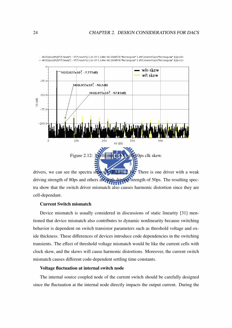
are all ideal devices including switches, resistors and current sources. Figure 2.12 shows
that the black line is the spectrum of DAC output without clock skew, and the yellow
color one is the spectrum of DAC output with clock skew. It’s clearly, that the clock skew
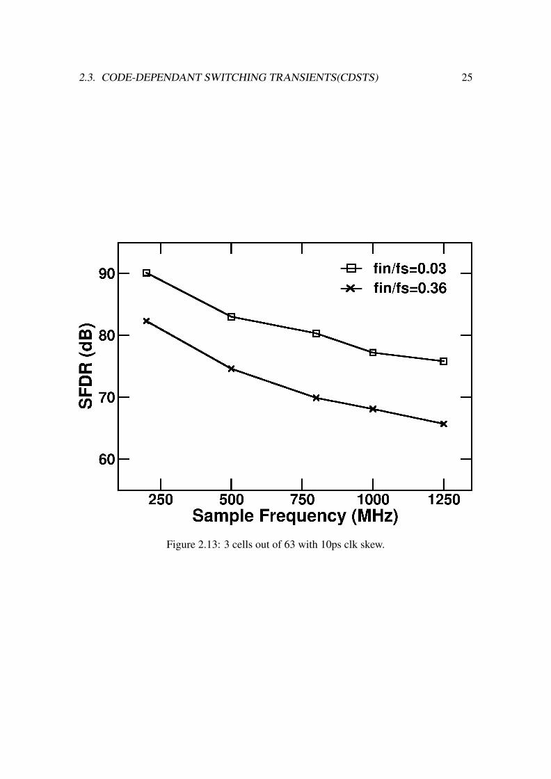
induces harmonic distortions. In Figure 2.13, x axis is sampling frequency and y axis
is SFDR. The upper line is the SFDR of DAC with lower output frequency. When the
sampling clock, Fs, is 250 MHz, the lower output frequency of 0.03Fs is with a 90dBc of
SFDR and the higher one of 0.36Fs is 82dBc. Because the clock skew is cell-dependant,
the high frequency input will have more switching switches. As the sampling frequency
increased, the SFDR of the both line drops dramatically due to the shorter clock period.
Switch driver mismatch
Switch driver mismatch may result in different rising time and falling time or asym-
metry rising/falling time [39, 28]. Then, the glitch area or glitch energy becomes cell-
dependant. This phenomenon is severe for the high-speed DAC since the glitch area of
one sampling period increases with the sampling frequency. Next, we run a simulation
by a 12-bit DAC with 6-6 segmentation. The simulation condition is with ideal current
sources and behavioral switch drivers. By setting different driving strength of the switch
24 CHAPTER 2. DESIGN CONSIDERATIONS FOR DACS
Figure 2.12: 3 cells out of 63 with 10ps clk skew.
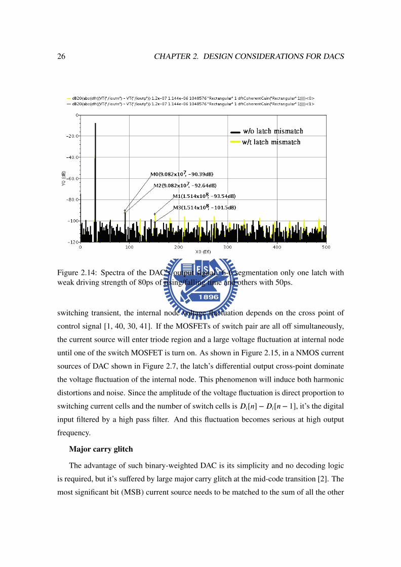
drivers, we can see the spectra shown in Figure 2.14. There is one driver with a weak
driving strength of 80ps and others are with driving strength of 50ps. The resulting spec-
tra show that the switch driver mismatch also causes harmonic distortion since they are
cell-dependant.
Current Switch mismatch
Device mismatch is usually considered in discussions of static linearity [31] men-
tioned that device mismatch also contributes to dynamic nonlinearity because switching
behavior is dependent on switch transistor parameters such as threshold voltage and ox-
ide thickness. These differences of devices introduce code dependencies in the switching
transients. The effect of threshold voltage mismatch would be like the current cells with
clock skew, and the skews will cause harmonic distortions. Moreover, the current switch
mismatch causes different code-dependent settling time constants.
Voltage fluctuation at internal switch node
The internal source coupled node of the current switch should be carefully designed
since the fluctuation at the internal node directly impacts the output current. During the
2.3. CODE-DEPENDANT SWITCHING TRANSIENTS(CDSTS) 25
Figure 2.13: 3 cells out of 63 with 10ps clk skew.
26 CHAPTER 2. DESIGN CONSIDERATIONS FOR DACS
Figure 2.14: Spectra of the DAC’s output signal. 6-6 segmentation only one latch withweak driving strength of 80ps of rising/falling time and others with 50ps.
switching transient, the internal node voltage fluctuation depends on the cross point of
control signal [1, 40, 30, 41]. If the MOSFETs of switch pair are all off simultaneously,
the current source will enter triode region and a large voltage fluctuation at internal node
until one of the switch MOSFET is turn on. As shown in Figure 2.15, in a NMOS current
sources of DAC shown in Figure 2.7, the latch’s differential output cross-point dominate
the voltage fluctuation of the internal node. This phenomenon will induce both harmonic
distortions and noise. Since the amplitude of the voltage fluctuation is direct proportion to
switching current cells and the number of switch cells is Di[n]−Di[n− 1], it’s the digital
input filtered by a high pass filter. And this fluctuation becomes serious at high output
frequency.
Major carry glitch
The advantage of such binary-weighted DAC is its simplicity and no decoding logic
is required, but it’s suffered by large major carry glitch at the mid-code transition [2]. The
most significant bit (MSB) current source needs to be matched to the sum of all the other

2.4. CODE-DEPENDANT LOADING VARIATION (CDLV) 27
Cross−A Cross−B Cross−C Cross−D
Internal NodeFluctuation
Latch’s
Cross−point
Figure 2.15: The latch’s differential output cross-point dominate the voltage fluctuationof the internal node.
Iu
Vo1 Vo2
LRLR
IuuR Cu
Vo1 Vo2
LR LR
Vo1 Vo2
LR LR
Co1o1R o2RCo2 Io2Io1
Figure 2.16: Code-dependent loading variation (CDLV).
current sources to within 0.5 LSB’s (least significant bits). That is, the maximum DNL
locates at the mid-code transition. The miscode glitch contains highly nonlinear signal
components and will manifest itself as spurs in the frequency domain. Thermometer
weighted DAC can avoid this major carry glitch, but the cost is unacceptable for high
resolution DACs. The DACs are designed with less major carry glitch and lower cost than
thermometer weighted by segmentation. The degree of segmentation influence on both
the structure of the converter and on its performance.

28 CHAPTER 2. DESIGN CONSIDERATIONS FOR DACS
2.4 Code-dependant Loading Variation (CDLV)
Figure 2.16 shows another source of harmonic distortion. Each current cell is modeled
as an ideal switch on top of an ideal current source Iu in parallel with a resistor Ru and
a capacitor Cu. The resistor Ru represents the output resistance of the current source.
The capacitor Cu represents the capacitance associated with the output node of the cur-
rent source, including the gate capacitance of the current switch. Both Ru and Cu are
connected to either the Vo1 node or the Vo2 node, depending on the state of the switch.
As a result, the total loadings for output nodes Vo1 and Vo2 vary with digital input Di[k].
This code-dependent loading variation (CDLV) effect introduces harmonic distortion in
the differential output Vo = Vo1 − Vo2. When Di[k] is a sinewave, the 3rd-order harmonic
distortion caused by the CDLV effect is [42, 43, 34, 12]
HD3 =[
M
4·RL.d
|Zu|
]2
(2.3)
where M is the total number of current cells, RL,d = 2RL is the differential resistance of
the DAC output loads, and Zu is the output impedance of a single current cell, where
1Zu
=1
Ru + jωCu. (2.4)
In single-ended application, the CDLV would cause second harmonic distortion
HD2 = −20log[(
MRL
4Zu + 2MRL
)]
(2.5)
For NMOS DAC shown in Figure 2.17, theZu in Equation (2.4) is the output impendence
look into the current cell. The simulated results of Zu is drawn in Figure 2.18. The Zo
is dominated by Ru at low frequency, as the frequency is increased then Zu is dominated
by Cu. The slope of Zo versus frequencies in log scale is -1. If the DAC is 12-bit with
6-6 segmentation, there are 63 MSB’s current cells and 6 LSB’s current cells which can
be treated as one MSB cell. In other words, M is 64 in Equation (4.1). Assume that
RL.d is 50 Ω. The -70 dB HD3 requirement is that Zu must larger than 45 kΩ. Refer to
the Figure 2.18, the Zu is 45 kΩ at output frequency equal to 84 MHz. The -70dB HD3
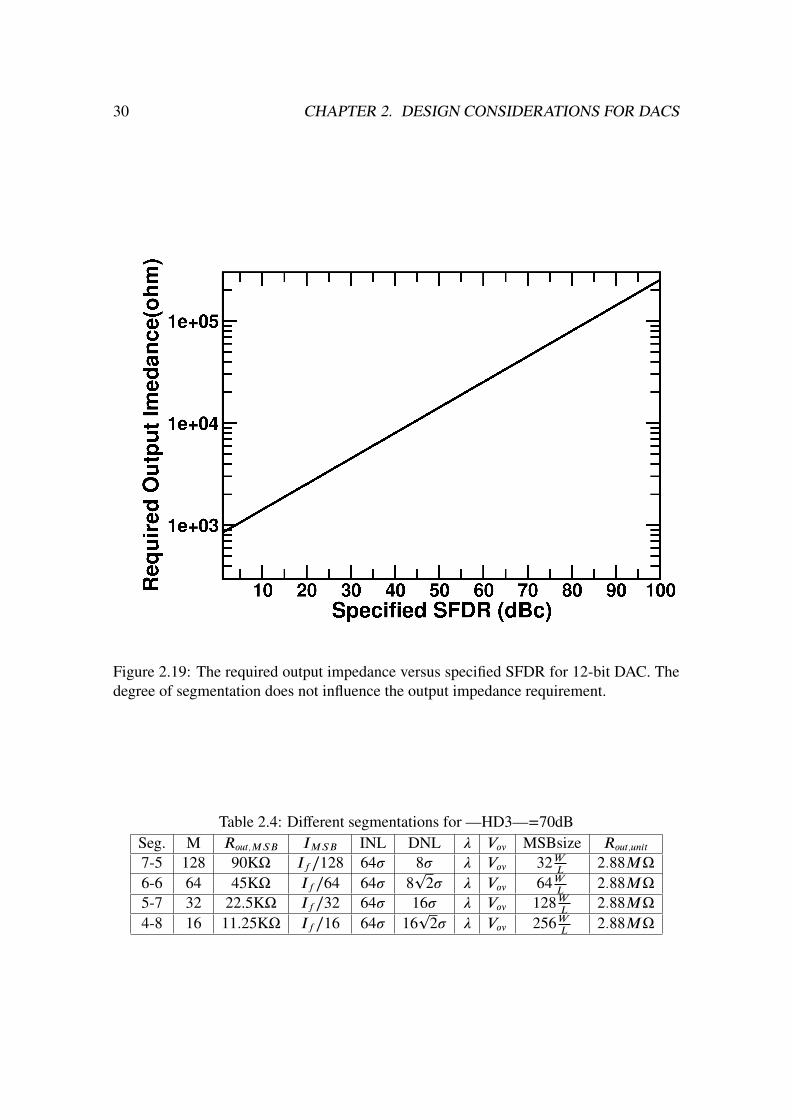
bandwidth is limited by the large Cu. For the 12-bit, 6-6 segmentation DAC, Figure 2.19
shows the required output impedance versus specified SFDR. If the target SFDR is higher,

2.4. CODE-DEPENDANT LOADING VARIATION (CDLV) 29
Zo
Figure 2.17: Zu isthe simulated outputimpedance of onecurrent cell when oneswitch is off.
Figure 2.18: The frequency response of Zu
output impedance requirement is more strict. In Figure 2.21, we also plot the limitation
of HD2 and HD3 which are described in Equation (2.5) and Equation (4.1).
The equation describes the maximum single-end INL at middle code [44].
INL =IunitR
2LM
2
4Rout
(2.6)
This is the CDLV effect in static performance. If the INL of DAC is specified to 0.5 LSB,
the required output impedance can be obtained from the equation Equation (2.6). The re-
quired impedance of different resolutions are plotted in Figure 2.21 [42, 43]; nevertheless,
the required impedance challenge is not for static linearity since the impedance is easy to
be reached.
As shown in Table 2.4, segmentation does not impact the output impedance require-
ment. For example, a 12-bit DAC with 7-5 segmentation needs 90 KΩ, and the unit
current cell needs 2.88 MΩ. However, 12-bit DAC with 4-8 segmentation has the same
impedance requirement for the unit current cell.
Increasing Ru and reducing Cu can mitigate the CDLV effect. Adding cascode stage
to a current source can increase Ru. In most designs, the CDLV effect at high frequencies
30 CHAPTER 2. DESIGN CONSIDERATIONS FOR DACS
Figure 2.19: The required output impedance versus specified SFDR for 12-bit DAC. Thedegree of segmentation does not influence the output impedance requirement.
Table 2.4: Different segmentations for —HD3—=70dBSeg. M Rout,MSB IMSB INL DNL λ Vov MSBsize Rout,unit
7-5 128 90KΩ If/128 64σ 8σ λ Vov 32WL
2.88MΩ6-6 64 45KΩ If/64 64σ 8
√2σ λ Vov 64W
L2.88MΩ
5-7 32 22.5KΩ If/32 64σ 16σ λ Vov 128WL
2.88MΩ4-8 16 11.25KΩ If/16 64σ 16
√2σ λ Vov 256W
L2.88MΩ
2.4. CODE-DEPENDANT LOADING VARIATION (CDLV) 31
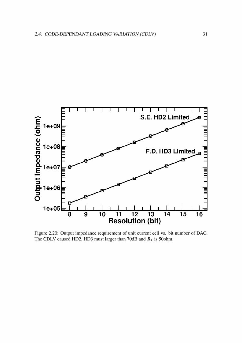
Figure 2.20: Output impedance requirement of unit current cell vs. bit number of DAC.The CDLV caused HD2, HD3 must larger than 70dB and RL is 50ohm.
32 CHAPTER 2. DESIGN CONSIDERATIONS FOR DACS
Figure 2.21: Output impedance requirement of unit current cell vs. bit number of DAC.The single ended INL caused by CDLV must small than 0.5LSB and RL is 50ohm.
2.5. SUMMARY 33
is dominated by Cu. The Cu capacitance is determined by the device dimensions of the
current switch and the current source, while the device dimensions are governed by the
matching requirements.
The CDLV effect can be mitigated by adding an additional cascode stage following the
current switch in each current cell [33, 7, 34]. The MOSFETs in those cascode stages need
to have large transconductances to achieve good high-frequency performance [34, 12].
2.5 Summary
In this section, we discuss most of the design considerations for high speed current-
steering DACs. The key point is to reduce the parasitic loading on the signal path for high
signal bandwidth. And carefully chose the size of switch, cross point the switches, layout
matching and tree-shape routing for same time constant. Moreover, techniques such as
calibration, DEM and return-to-zero can be used but must evaluate the extra penalty.

34 CHAPTER 2. DESIGN CONSIDERATIONS FOR DACS

Chapter 3
A 8-Bit 1.6 GS/s 90 nm CMOS DAC
3.1 Introduction
The current-steering digital-to-analog converts (DACs) can achieve high sampling rate,
and thus are commonly used in generating high-frequency signals [6, 1, 7, 10, 34]. Fig-
ure 3.1 shows a generic current-steering DAC. It consists of M equally-weighted cur-
rent cells. Each current cell contains a current source of Iu output current, a p-channel
MOSFET pair functioning as a current switch, and a digital latch controlled by a clock
CK. The complementary outputs of the latch control the current switch, directing the Iucurrent to either the RL load at Vo1 or the one at Vo2. A decoder converts the DAC dig-
ital input Di[k] into M thermometer-code signals Bj[k], where 1 ≤ j ≤ M , such that
Di[k] =∑M
j=1 Bj[k]. The Bj[k] signal has a binary value of either +1 or −1. Figure 3.2
illustrates the DAC differential non-return-to-zero (NRZ) output waveform Vo = Vo1−Vo2.
The Vo has a voltage range between +MIuRL and −MIuRL, and a step size of 2IuRL.
The DAC static linearity, specified as differential nonlinearity (DNL) and integral non-
linearity (INL), is mainly determined by the matching of Iu among different current cells
and the output resistances of the Iu current sources. There are techniques to improve
the static linearity, which will not be covered in this section. However, even with ideal
Iu current sources, dynamic nonlinearity still occurs. It is manifested as spurious-free
dynamic range (SFDR) degradation shown in the Vo output spectrum when the Di[k]
input is a single-tone sinewave. The SFDR decreases rapidly with increasing input fre-
35

36 CHAPTER 3. A 8-BIT 1.6 GS/S 90 NM CMOS DAC
LRLR
Vo1 Vo2
jB
Di
Iu
[k]
[k]
Dec
oder
CK
Latc
h
Figure 3.1: A current-steering DAC.
quency. The sources of dynamic nonlinearity are numerous and complex, including code-
dependent switching transients [31, 38] and capacitive output impedance of the current
cells [42, 34, 43].
The return-to-zero (RZ) technique has been proposed to improve the DAC dynamic
performance [31, 15, 18]. The technique adds an output buffer to isolate the output loads
from the current switches and executes current switching operation during the zero phase.
The DAC dynamic performance can also be improved by modifying the current switching
operation to make the switching transients uncorrelated with the input sequence [45, 1,
24].
In this section, we propose a digital random return-to-zero (DRRZ) technique to miti-
gate the effect of switching transients on the DAC dynamic performance. A 8-bit 1.6-GS/s
current-steering DAC chip was designed to demonstrate the proposed technique.

3.2. DIGITAL RANDOM RETURN-TO-ZERO (DRRZ) 37
Di Di Di Di
Vo
[1] [2] [3] [4]
CK
t
Figure 3.2: Non-return-to-zero (NRZ) output waveform of a current-steering DAC.
Vo
Di Di Di Di[1] [2] [3] [4]
CK
t
Z[1] Z[2] Z[3] Z[4]
Figure 3.3: Waveforms of a return-to-zero (RZ) DAC.
3.2 Digital Random Return-to-Zero (DRRZ)
Consider the j-th current cell of the DAC shown in Figure 3.1. Its current switch is
driven by Bj[k] ∈ −1,+1. When CK changes from low to high, the current switch
may remain unchanged or undergo a (−1)-to-(+1) switching or a (+1)-to-(−1) switching.
When the current switch makes a switching, the DAC output Vo experiences a transient
disturbance called switching transient. The (−1)-to-(+1) switching transient and (+1)-
to-(−1) switching transient have opposite polarities. For the NRZ DAC, the switching
of the current cells is determined by the input Di[k]. Thus, the switching transients are
input-dependent and will result in DAC dynamic distortion.
Analog return-to-zero (ARZ) has been used to hide the switching transients from the
38 CHAPTER 3. A 8-BIT 1.6 GS/S 90 NM CMOS DAC
Di Di Di Di
Bj
Bj Bj BjBj Rj Rj Rj Rj
[1] [2] [3] [4]Z[1] Z[2] Z[3] Z[4]
1 11 1 1 1 1 1 1 11 1
CK
[2] [3] [4][1] [1] [2] [3] [4]
Figure 3.4: Switching behavior of a current cell in a digital return-to-zero (DRZ) DAC ora digital random return-to-zero (DRRZ) DAC.
output [31, 15, 18]. The CK and Vo waveforms of Figure 3.3 show the ARZ operation.
When CK is high, the DAC is in the data phase. It decodes the digital input Di[k], sets up
its internal current switches, and generates an analog output Vo corresponding to Di[k].
When CK is low, the DAC is in the zero phase. The DAC output Vo is forced to zero by
analog switches added at output nodes Vo1 and Vo2. The current switches in the DAC are
switched to reflect the next input Di[k + 1] during the zero phase. Thus, the switching
transients do not appear in Vo to contribute dynamic distortion. The analog switches at the
output nodes must be large enough to eliminate switching transients.
We can generate the RZ Vo waveform without using the analog switches at the output
nodes. As shown in Figure 3.3, when CK is low, the DAC is in a zero phase, Z[k], in
which the DAC arranges its internal current switches in such a way that output Vo = 0.
In the Z[k] state, the switch controls, Bj[k], are reset to pre-defined values such that∑M
j=1 Bj[k] = 0, assuming M is an even number. However, in this digital return-to-
zero (DRZ) setup, switching transients appear in Vo. Consider the j-th current cell. The
sequence of its switching control, Bj, is shown in Figure 3.4. When CK is high, Bj =
Bj[k] is determined by the input Di[k]. When CK is low, Bj = Rj[k] is a fixed value
of either +1 or −1. In Figure 3.4, Bj[1] = +1 and Bj[2] = +1 have the same value. If
Rj[1] = +1, there will be no switching during the Z[1] period. If Rj[1] = −1, there will
be a (+1)-to-(−1) and a (−1)-to-(+1) transients on both edges of the Z[1] period. Also
shown in Figure 3.4, Bj[2] = +1 and Bj[2] = −1 have different values. If Rj[2] = +1, a
(+1)-to-(−1) transient occurs at the right edge of the Z[2] period. If Rj[2] = −1, a (+1)-
to-(−1) transient occurs at the left edge of the Z[2] period. In summary, the DRZ assigns
3.3. CIRCUIT DESCRIPTIONS 39
a constant to Rj[k], i.e., Rj[k] = +1 for all k or Rj[k] = −1 for all k. The current switch
transitions are determined by the Bj[k] sequence alone. Their strong correlation with the
input Di[k] yields distortion in Vo. The DRZ in fact introduces more input-dependent
switching transients than the NRZ.
We propose the digital random return-to-zero (DRRZ) technique to randomize the
switching transients appearing in DRZ. In this scheme, the switch controls Bj[k] in
the Z[k] phase are dictated by a pseudo random number generator (PRNG), such that∑M
j=1 Bj[k] = 0. Consider the j-th current cell and the operation sequence shown in Fig-
ure 3.4. When CK is high, Bj = Bj[k] is determined by the input Di[k]. When CK is
low, Bj = Rj[k] becomes a binary random variable which has a value of either +1 or −1.
In Figure 3.4, Bj[1] = +1 and Bj[2] = +1 have the same value. Switch transitions occur
only if Rj[1] = −1. Also shown in Figure 3.4, Bj[2] = +1 and Bj[2] = −1 have different
values. A switch transition occurs at the right edge of the Z[2] period if Rj[2] = +1. On
the other hand, a switch transition occurs at the left edge of theZ[2] period ifRj[2] = −1.
In summary, the DRRZ makes Rj[k] a random sequence, which randomizes the current
switch transitions. When the switching transients are not correlated with the input Di[k],
they appear as noises in Vo and will not cause distortion.
3.3 Circuit Descriptions
Figure 3.5 shows the block diagram of the 8-bit DAC. It is segmented into a 5-bit equally-
weighted MSB DAC (M-DAC) and a 3-bit binary-weighted LSB DAC (L-DAC). The
M-DAC comprises 31 identical current cells. Each current cell can output an current of
8I , where I is the DAC unit current. The L-DAC comprises 4 current cells which output
an current of 1I , 1I , 2I , and 4I respectively. There are two 1I current cells in the L-DAC
so that a differential output of zero can be realized. The node Io1 and node Io2 of all current
cells are tied together respectively to form the two differential DAC output terminals. The
two output terminals are connected to two RL resistors to generate the differential Vo as
illustrated in Figure 3.1. When CK is high, the decoder controls both the M-DAC and the
L-DAC. The current of the extra 1I current cell in the L-DAC is always directed to the
Io1 node. The DAC output is expressed as Vo[k] = (Di[k] − 127) × 2IRL, where Di[k]

40 CHAPTER 3. A 8-BIT 1.6 GS/S 90 NM CMOS DAC
Di
jR
jB
Io1 Io2
Io1 Io232R
Dec
od
er
[k]
PR
NG
[k]
[k]
[k]
31
8
4
32
31
CK
MU
X L
at
31 MSB Current Celles
CK
MU
X L
at
2I 4I
8I
1I1I
Figure 3.5: DAC block diagram.

3.3. CIRCUIT DESCRIPTIONS 41
is an integer from 0 to 255. In our design, I = 80 µA and RL = 25 Ω yield a Vo with a
differential signal range of 1 Vpp.
In this work the devices were sized to fit the 8-bit linearity by matching equation
Equation (3.1).
σ2∆II
=12×
1W · L
· (4A2
V T
Vov+ A2
β) (3.1)
For 8-bit with 5-3 segmentation, LSB = 1 2 4, MSB = 8 8 8 ...
INL (max)√
256σ ≤ 0.5LSB
DNL(max)√
16σ ≤ 0.5LSB
1 ×√
256σ ≤ 0.5
σ ≤ 3.125 × 10⁻²
2 × (3.125 × 10−2)2 ×WLunit ≥ 4 ·5.812
V 2ov
+ 0.01622
Vov (mV ) 100 150 200 250 300 350
WLunit (um2)(1σ) 14.1/2 6.4 3.7 2.5 1.8 1.1
WLunit (um2)(3σ) 127/2 57.6 33.3 22.5 16.2 9.9
σ ×1.0 ×1.4 ×1.6 ×1.8 ×2 ×2.2 ×2.4 ×2.6 ×2.8 ×3.0
yield 68.3 77.0 83.8 89.0 92.8 95.4 97.2 98.4 99.1 99.7
As shown in Figure 3.5, each current cell contains a multiplexing latch. When CK is
high, the latch selects the Bj[k] control from the Di[k] decoder for normal DAC output.
When CK is low, the latch selects the Rj[k] control from a PRNG. The PRNG is a 16-bit
linear feedback shift register. Its 16 outputs and their complements form the 32 Rj[k]
zero-phase controls. This arrangement ensures that∑32
j=1 Rj[k] = 0. During the zero

42 CHAPTER 3. A 8-BIT 1.6 GS/S 90 NM CMOS DAC
VB1
VB2
Io1 Io2
jBjB jR jR
CK
[k][k]
CK
VDD=1.2VMUX−Latch
M1
M2
M3 M4
[k] [k]
M11 M12 M16M15
M13 M17M14 M18
VDD=2.5V
Figure 3.6: Current cell schematic.
phase, the entire L-DAC is treated as a single MSB current cell controlled by a single
R32[k] signal.
Figure 3.6 shows the circuit schematic of a current cell. MOSFETs M1 and M2 form
a cascode current source. M3 and M4 together function as a current switch. The current
source is operated under a 2.5 V supply. M1–M4 are MOSFETs with thick gate oxide.
MOSFETs M11–M18 and the two inverters form a level-sensitive MUX-latch. When CK
is high, the Bj[k] signal is loaded into the latch. When CK is low, the Rj[k] signal is
loaded into the latch. The MUX-latch is operated under a 1.2 V supply.
As shown in Figure 3.7 sine-wave was translated to fully differential by off-chip trans-
former, and a internal differential to single ended amplifier was used before flip-flop which
divided the clock by two. With the division function, duty cycle of clock is near to fifty
percentages to avoid timing error between digital and analog interface. The digital circuit
dealt with data phase signal at rising edge of digital clock and zero phase signal at the
falling edge. The analog clock was above 180 degree differ from digital clock; there-
fore, level-sensitive MUX-Latch could catch the proper digital signal. For measurement,
3.4. EXPERIMENTAL RESULTS 43
Digital clock : CLKD
Analog clock : CLKA
F/F
Data phasesignal
Zero phasesignal
Buffer
Buffer
CLKD
CLKA
Figure 3.7: Clock buffer and interface timing between digital and analog
a direct digital frequency synthesizer (DDFS) was imbedded. All the digital part were
implemented by synthesis and auto place and route.
3.4 Experimental Results
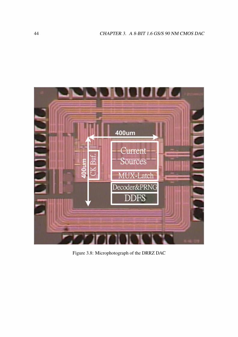
The DAC was fabricated in a standard 90 nm CMOS technology. Figure 3.8 shows the
chip photograph. The DAC core area is 400×400 µm2. The chip also includes a direct dig-
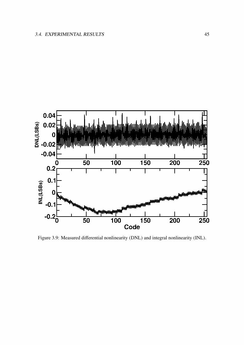
ital frequency synthesizer (DDFS) to generate digital inputs for DAC testing. Figure 3.9
shows the measured differential nonlinearity (DNL) and integral nonlinearity (INL) of
the DAC. The DNL is +0.04/−0.03 LSB and the INL is +0/−0.2 LSB.
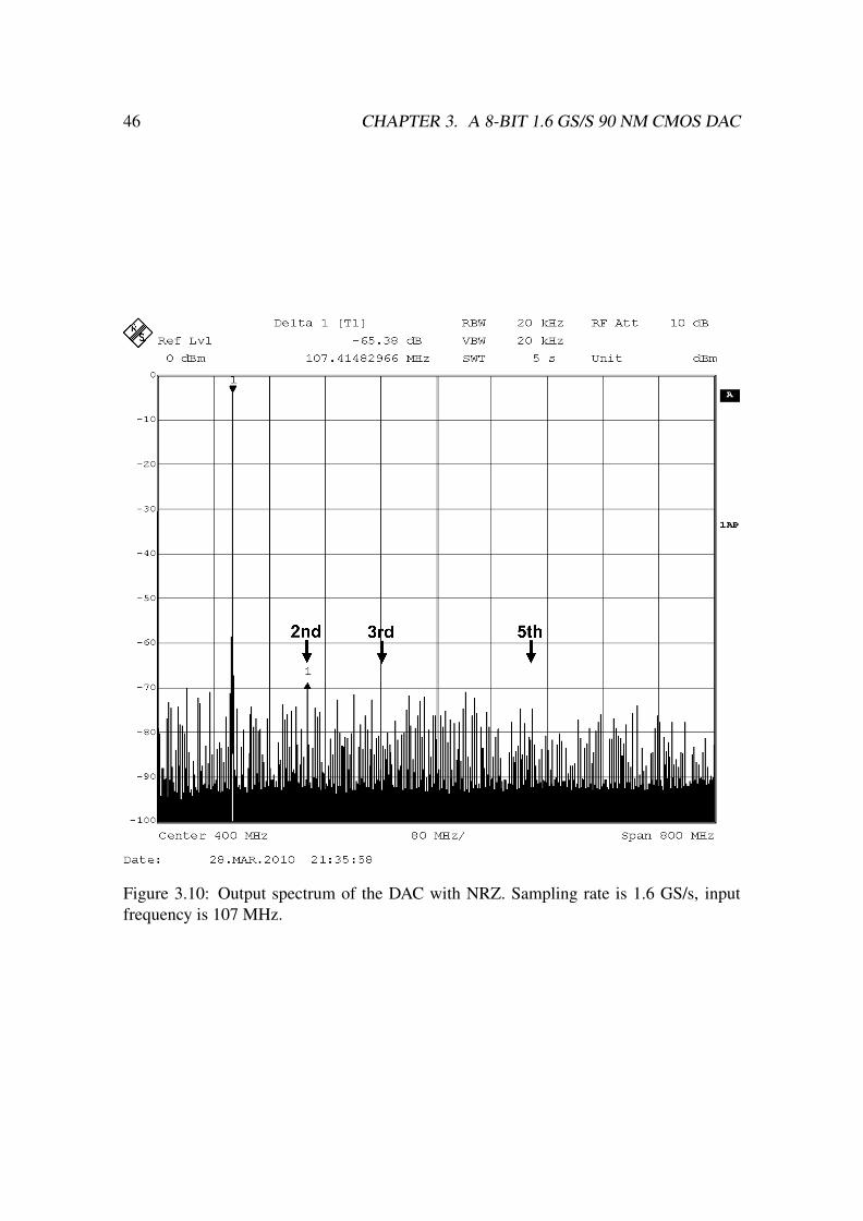
Figure 3.10 and Figure 3.11 show the output spectra of the DAC operating at 1.6 GS/s
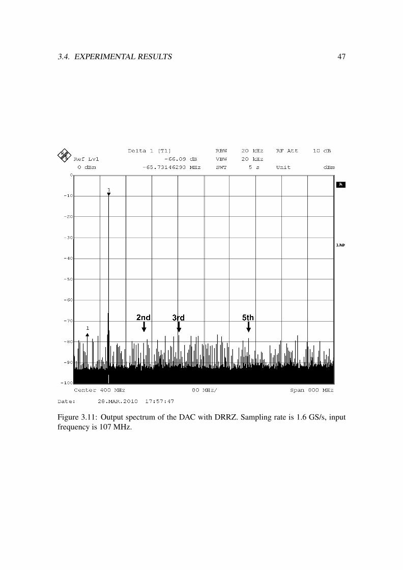
sampling rate, and the input frequency is 107 MHz. For Figure 3.10, the DRRZ function
is turned off, and the DAC output waveform is similar to the NRZ Vo waveform shown
in Figure 3.2. For Figure 3.11, the DRRZ function is turned on, and the DAC output
waveform is similar to the RZ Vo waveform shown in Figure 3.3. There are no significant
harmonic tones in both figures. The measured SFDR is 65.4 dB for the NRZ DAC and
44 CHAPTER 3. A 8-BIT 1.6 GS/S 90 NM CMOS DAC
Figure 3.8: Microphotograph of the DRRZ DAC
3.4. EXPERIMENTAL RESULTS 45
Figure 3.9: Measured differential nonlinearity (DNL) and integral nonlinearity (INL).
46 CHAPTER 3. A 8-BIT 1.6 GS/S 90 NM CMOS DAC
Figure 3.10: Output spectrum of the DAC with NRZ. Sampling rate is 1.6 GS/s, inputfrequency is 107 MHz.
3.4. EXPERIMENTAL RESULTS 47
Figure 3.11: Output spectrum of the DAC with DRRZ. Sampling rate is 1.6 GS/s, inputfrequency is 107 MHz.

48 CHAPTER 3. A 8-BIT 1.6 GS/S 90 NM CMOS DAC
Figure 3.12: Output spectrum of the DAC with NRZ. Sampling rate is 1.6 GS/s, inputfrequency is 731 MHz.
66 dB for the DRRZ DAC. When the input frequency of the DAC is low, the total number
of current switches forced to switch is low in each clock cycle. The overall switching tran-
sients have little effect on the harmonic distortion of the DAC. Thus, the DRRZ function
shows little improvement in SFDR.
Figure 3.12 and Figure 3.13 are DAC output spectra under similar conditions except
the input frequency is raised to 731 MHz. When the input frequency of the DAC is
high, the total number of current switches forced to switch is high in each clock cycle.
The effect of switching transients becomes large and is revealed as the harmonic tones in
Figure 3.12. The SFDR is 43 dB and is dominated by the third harmonic. The harmonic
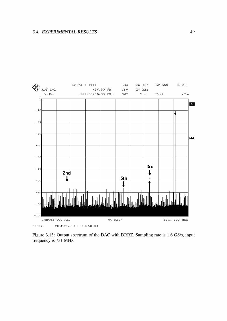
3.4. EXPERIMENTAL RESULTS 49
Figure 3.13: Output spectrum of the DAC with DRRZ. Sampling rate is 1.6 GS/s, inputfrequency is 731 MHz.

50 CHAPTER 3. A 8-BIT 1.6 GS/S 90 NM CMOS DAC
0 200 400 600 800Output Signal Frequency (MHz)
40
50
60
70
80
SF
DR
(d
B)
DRRZ
DRZ
NRZ
|20log HD3|
Figure 3.14: Measured SFDR at different signal frequencies.
tones are suppressed by the DRRZ operation as illustrated in Figure 3.13. The SFDR is
improved to 56.5 dB.
Figure 3.14 shows the measured SFDR of the DAC operated at 1.6 GS/s sampling rate
and with different input frequencies. The DAC has three different configurations, which
are NRZ, DRZ, and DRRZ. For the NRZ DAC, the measured SFDR is degraded from
65 dB to 42 dB as input frequency increases toward 800 MHz. Employing the DRRZ
operation, the DAC can maintain a SFDR larger than 60 dB up to 460 MHz and a SFDR
larger than 55 dB up to 800 MHz. Figure 3.14 also shows the measured SFDR of the DRZ
DAC. The DRZ setup cannot improve SFDR at all. At low frequencies, the DRZ DAC
exhibits a SFDR even worse than the NRZ DAC. This is because, at low frequencies, DRZ
introduces more switching transients than NRZ.
Also shown in Figure 3.14 is a theoretical HD3 calculation by considering only the

3.4. EXPERIMENTAL RESULTS 51
Table 3.1: DAC Performance SummaryTechnology CMOS 90 nmResolution 8 BitsSampling Rate fs 1.6 GS/sDNL +0.04 / −0.03 LSBINL +0.0 / −0.2 LSBSFDR @fin = 100 MHz 64.5 dBSFDR @fin = 700 MHz 57.0 dBLoad Current 20 mAOutput Swing 1 VppSupply Voltage (Analog/Digital) 2.5 V / 1.2 VPower Consumption 90 mWCore Area 0.16 mm2
output impedance of current cells [42, 34, 43]. It is expressed as
HD3 =[
M
4·RL,d
|Zo|
]2
(3.2)
where RL,d = 50 Ω is the differential resistance of the DAC output loads, M = 32 is the
total number of M-DAC current cells, andZo is the output impedance of a M-DAC current
cell. The L-DAC is treated as a single M-DAC current cell. Referring to Figure ??, Zo
is the output impedance looking into the Io1 terminal when M3 is turned on and M4 is
off. The Zo in our design can be modeled as a resistor Ro = 1.9 MΩ in parallel with a
capacitor Co = 10.8 fF. Figure 3.14 indicates that the HD3 of Equation (3.2) is the major
distortion source for the DRRZ DAC with input frequencies higher than 300 MHz. This
type of distortion cannot be removed by DRRZ.
The DAC specifications are summarized in Table 4.2. Figure 3.15 compares the dy-
namic performance of this DAC against other published DAC works. In order to compare
DACs of different sampling rates, the dynamic performance is defined as SFDR × fs,
where SFDR is expressed in power ratio and fs is sampling rate in Hz. Note the reported
DAC is only an 8-bit design. But its dynamic performance is competitive at high signal
frequencies.

52 CHAPTER 3. A 8-BIT 1.6 GS/S 90 NM CMOS DAC
10 100 1000Output Signal Frequency (MHz)
108
109
1010
1011
SFD
R x
f s
[11][5]
[1]
[6]
[9]
[8]
[3]
This Work
Figure 3.15: Dynamic performance comparison of published DACs.

3.5. SUMMARY 53
3.5 Summary
A CMOS 8-bit 1.6-GS/s current-steering DAC was presented to demonstrate the proposed
digital random return-to-zero (DRRZ) technique. The technique requires only a small
overhead in digital circuits. The improvement in SFDR of the DAC is 14 dB when the
input frequency is 800 MHz.

54 CHAPTER 3. A 8-BIT 1.6 GS/S 90 NM CMOS DAC
Chapter 4
A 12-Bit 1.25-GS/s Background
Calibrated DAC
4.1 Introduction
The current-steering digital-to-analog converts (DACs) can achieve high sampling rate,
and thus are commonly used in generating high-frequency signals [6, 1, 7, 8, 4, 10, 34,
12]. Figure 4.1 shows a generic current-steering DAC. It consists of M equally-weighted
current cells. Each current cell contains a current source of Iu output current, a MOSFET
pair functioning as a current switch, and a digital latch controlled by a clock CK. The
complementary outputs of the latch control the current switch, directing the Iu current
to either the RL load at Vo1 or the one at Vo2. A decoder converts the DAC digital input
Di[k] into M thermometer-code signals Bj[k], where 1 ≤ j ≤ M . We define the Bj[k]
signal has a binary value of either +1 or −1. Figure 4.1 illustrates the DAC differential
non-return-to-zero (NRZ) output waveform Vo = Vo1 − Vo2. The Vo has a voltage range
between +MIuRL and −MIuRL, and a step size of 2IuRL.
The DAC static linearity, specified as differential nonlinearity (DNL) and integral non-
linearity (INL), is mainly determined by the matching of Iu among different current cells
and the output resistances of the Iu current sources. Cascode technique is usually used
to increase the output resistance of a current source. The dimension of the transistors
in the current sources must be large enough to ensure good Iu matching [13]. There
55

56 CHAPTER 4. A 12-BIT 1.25-GS/S BACKGROUND CALIBRATED DAC
Vo1 Vo2
LRLR
jB
Di
Iu
Di Di Di Di
Vo
[k]
Dec
oder
[k]
[1] [2] [3] [4]
Latc
h
CK
M
CK
t
Figure 4.1: A current-steering DAC.
4.2. DESIGN FOR HIGH SIGNAL BANDWIDTH 57
are techniques that can relax the device matching requirements, including calibrations
[14, 15, 17, 18, 20] and dynamic element matching [24].
Besides static linearity, dynamic performance is also crucial for a high-speed DAC.
The DAC dynamic performance is manifested as spurious-free dynamic range (SFDR)
degradation shown in the output spectrum of Vo when the Di[k] input is a single-tone
sinewave. As for a DAC with poor dynamic performance, its SFDR decreases rapidly with
increasing input frequency. The DAC dynamic performance is related to the switching
operation of the internal current switches. It induces the code-dependent switch transient
(CDST) effect [31, 38, 28] and the code-dependent loading variation (CDLV) effect [42,
34, 43, 12].
This section describes a 12-bit 1.25-GS/s current-steering DAC [35]. We employ the
digital random return-to-zero (DRRZ) technique [32] to mitigate the CDST effect and
relax matching requirement for current switches. The DRRZ operation also enables a
current-cell background calibration. The calibration relaxes the device matching require-
ments for the Iu current sources, allowing a more compact design of the current cells. The
compact current cell design directly reduces the CDLV effect. The DAC was fabricated
using a standard 90 nm CMOS technology. At 1.25 GS/s sampling rate, this DAC chip
achieves a SFDR better than 70 dB up to 500 MHz input frequency.
4.2 Design for High Signal Bandwidth
Figure 4.2 shows the operation of a single current cell. The current cell contains a current
source Iu and a MOSFET current switch M1-M2. Upon the rising edge of clock CK,
the binary input Bj[k] is loaded into the latch. Its two complementary outputs, Vs1 and
Vs2, drive the current switch, directing the Iu current to either output node Vo1 or output
node Vo2. Figure 4.2 also shows the transient response of the differential output current
Io = Io1 − Io2. The output current Io is a combination of an ideal transient response and
switching transients. Switching transients occur only whenBj[k] varies. There are several
sources for switching transients [31], including switch feedthrough through the current
switch, timing skew of CK, finite rise/fall time of Vs1 and Vs2, and voltage fluctuation at
the common-source node Va.
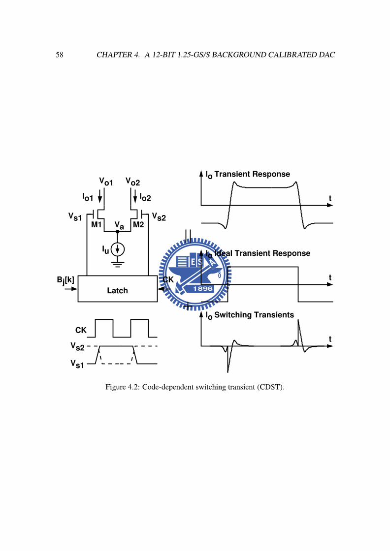
58 CHAPTER 4. A 12-BIT 1.25-GS/S BACKGROUND CALIBRATED DAC
Io
Io
Io
Vs1
Vs2
Vo1 Vo2
Io1 Io2
Vs1 Vs2Va
Iu
jB
Transient Response
Ideal Transient Response
Switching Transients
[k] t
t
t
CK
Latch
M1 M2
CK
Figure 4.2: Code-dependent switching transient (CDST).

4.2. DESIGN FOR HIGH SIGNAL BANDWIDTH 59
Iu
Vo1 Vo2
LRLR
IuuR Cu
Vo1 Vo2
LR LR
Vo1 Vo2
LR LR
Co1o1R o2RCo2 Io2Io1
Figure 4.3: Code-dependent loading variation (CDLV).
The Io switching transients from all current cells are summed up at the DAC Vo port.
Assume the switching transients are invariant and identical among all current cells, and
the switching transients at the rising edges of Io are the inverse of the switching transients
at the falling edges of Io. Then total switching transients appearing at Vo are proportional
to Di[k] − Di[k − 1]. These identical switching transients do not cause harmonic dis-
tortion. However, there are device variations in both the current switch and the latch,
and there are different CK timing skew for different current cells. Thus, different cur-
rent cells exhibits different switching transients. Depending on the Di[k] sequence, the
sequence of the switching transient summation becomes a nonlinear term, resulting in
harmonic distortions. This is called the CDST effect. If the input Di[k] is a single-tone
sinewave and its frequency is increased, the CDST effect is intensified due to the increase
of |Di[k] −Di[k − 1]|. Thus, the DAC SFDR decreases with increasing input frequency.
To reduce variation in switching transients, the Vs1 and Vs2 waveforms must be care-
fully designed. Matching among current switches, latches, and CK routes must be consid-
ered in the design. Adding a cascode stage to the current switch is also a common practice
to reduce feedthrough of Vs1 and Vs2 to the outputs.
Figure 4.3 shows another source of harmonic distortion. Each current cell is modeled
as an ideal switch on top of an ideal current source Iu in parallel with a resistor Ru and
a capacitor Cu. The resistor Ru represents the output resistance of the current source.
The capacitor Cu represents the capacitance associated with the output node of the cur-
rent source, including the gate capacitance of the current switch. Both Ru and Cu are

60 CHAPTER 4. A 12-BIT 1.25-GS/S BACKGROUND CALIBRATED DAC
connected to either the Vo1 node or the Vo2 node, depending on the state of the switch.
As a result, the total loadings for output nodes Vo1 and Vo2 vary with digital input Di[k].
This code-dependent loading variation (CDLV) effect introduces harmonic distortion in
the differential output Vo = Vo1 − Vo2. When Di[k] is a sinewave, the 3rd-order harmonic
distortion caused by the CDLV effect is [42, 43, 34, 12]
HD3 =[
M
4·RL.d
|Zu|
]2
(4.1)
where M is the total number of current cells, RL,d = 2RL is the differential resistance
of the DAC output loads, and Zu is the output impedance of a single current cell, where
1/Zu = 1/Ru + jωCu.
Increasing Ru and reducing Cu can mitigate the CDLV effect. Adding cascode stage
to a current source can increase Ru. In most designs, the CDLV effect at high frequencies
is dominated by Cu. The Cu capacitance is determined by the device dimensions of the
current switch and the current source, while the device dimensions are governed by the
matching requirements. The CDLV effect can be mitigated by adding an additional cas-
code stage following the current switch in each current cell [33, 7, 34]. The MOSFETs in
those cascode stages need to have large transconductances to achieve good high-frequency
performance [34, 12].
For this work, instead of adding additional cascode stages, we simply use smaller de-
vices for both the current sources and the current switches to reduce Cu. Smaller devices
lead to larger mismatches. However, due to the use of DRRZ, the matching requirement
for the current switches is relaxed. The mismatches among the current sources are cor-
rected by the current-cell background calibration described in Section 4.4.
4.3 DAC Architecture
Figure 4.4 shows the 12-bit DAC architecture. The DAC is segmented into a 6-bit equally-
weighted MSB DAC (M-DAC) and a 6-bit binary-weighted LSB DAC (L-DAC). The
differential output currents from both the M-DAC and the L-DAC are tied together and
connected to two external resistive loads RL1 and RL2 to produce the differential output
voltage Vo = Vo1 − Vo2. The M-DAC comprises 63 identical current cells. Each current

4.3. DAC ARCHITECTURE 61
Di[k]
jR [k]
Ic,j
Vo2Vo1
Lj[k]
0R [k]
Vo1 Vo2
Bj[k]
PR
NG
Dec
oder
48I
MU
X−L
atch
16I
M−DAC: 63 Equally−Weighted Current Cells
MU
X−L
atch
L−DAC: 7 Binary−Weighted Current Cells
64
63
63
CK
7
CK 8I, 16I, 32I1I, 1I, 2I, 4I
Figure 4.4: A segmented 12-bit DAC.
62 CHAPTER 4. A 12-BIT 1.25-GS/S BACKGROUND CALIBRATED DAC
1Q 2Q 32Q
0R 1R 2R 3R 63R
32Q31Q5Q4Q
D QD Q[k]
D Q[k] [k]
[k] [k] [k] [k] [k]
SwitchControl
[k][k]
[k][k]
CKCK CK
Switch Box
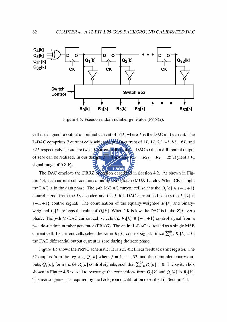
Figure 4.5: Pseudo random number generator (PRNG).
cell is designed to output a nominal current of 64I , where I is the DAC unit current. The
L-DAC comprises 7 current cells which output an current of 1I , 1I , 2I , 4I , 8I , 16I , and
32I respectively. There are two 1I current cells in the L-DAC so that a differential output
of zero can be realized. In our design, I = 4 µA and RL1 = RL2 = RL = 25 Ω yield a Vosignal range of 0.8 Vpp.
The DAC employs the DRRZ operation described in Section 4.2. As shown in Fig-
ure 4.4, each current cell contains a multiplexing latch (MUX-Latch). When CK is high,
the DAC is in the data phase. The j-th M-DAC current cell selects the Bj[k] ∈ −1,+1
control signal from the Di decoder, and the j-th L-DAC current cell selects the Lj[k] ∈
−1,+1 control signal. The combination of the equally-weighted Bj[k] and binary-
weighted Lj[k] reflects the value of Di[k]. When CK is low, the DAC is in the Z[k] zero
phase. The j-th M-DAC current cell selects the Rj[k] ∈ −1,+1 control signal from a
pseudo-random number generator (PRNG). The entire L-DAC is treated as a single MSB
current cell. Its current cells select the same R0[k] control signal. Since∑63
j=0 Rj[k] = 0,
the DAC differential output current is zero during the zero phase.
Figure 4.5 shows the PRNG schematic. It is a 32-bit linear feedback shift register. The
32 outputs from the register, Qj[k] where j = 1, · · · , 32, and their complementary out-
puts, Qj[k], form the 64 Rj[k] control signals, such that∑63
j=0 Rj[k] = 0. The switch box
shown in Figure 4.5 is used to rearrange the connections from Qj[k] and Qj[k] to Rj[k].
The rearrangement is required by the background calibration described in Section 4.4.
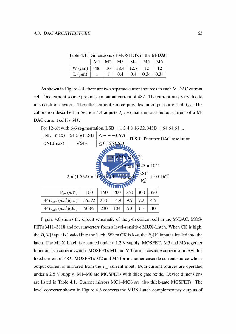
4.3. DAC ARCHITECTURE 63
Table 4.1: Dimensions of MOSFETs in the M-DACM1 M2 M3 M4 M5 M6
W (µm) 48 16 38.4 12.8 12 12L (µm) 1 1 0.4 0.4 0.34 0.34
As shown in Figure 4.4, there are two separate current sources in each M-DAC current
cell. One current source provides an output current of 48I . The current may vary due to
mismatch of devices. The other current source provides an output current of Ic,j. The
calibration described in Section 4.4 adjusts Ic,j so that the total output current of a M-
DAC current cell is 64I .
For 12-bit with 6-6 segmentation, LSB = 1 2 4 8 16 32, MSB = 64 64 64 ...INL (max) 64 × 1
2TLSB ≤ − − −LSB
DNL(max)√
64σ ≤ 0.125LSBTLSB: Trimmer DAC resolution
1 ×√
64σ ≤ 0.125
σ ≤ 1.5625 × 10⁻²
2 × (1.5625 × 10−2)2 ×WLunit ≥ 4 ·5.812
V 2ov
+ 0.01622
Vov (mV ) 100 150 200 250 300 350
WLunit (um2)(1σ) 56.5/2 25.6 14.9 9.9 7.2 4.5
WLunit (um2)(3σ) 508/2 230 134 90 65 40
Figure 4.6 shows the circuit schematic of the j-th current cell in the M-DAC. MOS-
FETs M11–M18 and four inverters form a level-sensitive MUX-Latch. When CK is high,
the Bj[k] input is loaded into the latch. When CK is low, theRj[k] input is loaded into the
latch. The MUX-Latch is operated under a 1.2 V supply. MOSFETs M5 and M6 together
function as a current switch. MOSFETs M1 and M3 form a cascode current source with a
fixed current of 48I . MOSFETs M2 and M4 form another cascode current source whose
output current is mirrored from the Ic,j current input. Both current sources are operated
under a 2.5 V supply. M1–M6 are MOSFETs with thick gate oxide. Device dimensions
are listed in Table 4.1. Current mirrors MC1–MC6 are also thick-gate MOSFETs. The
level converter shown in Figure 4.6 converts the MUX-Latch complementary outputs of
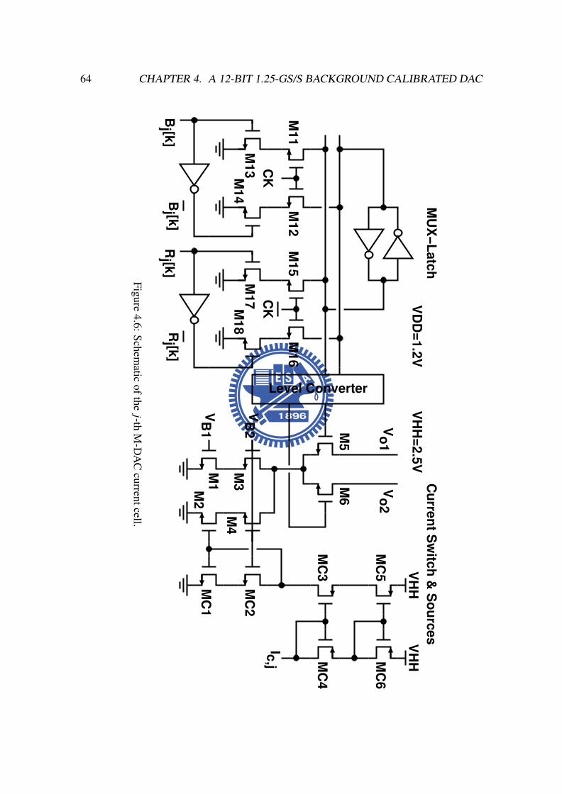
64 CHAPTER 4. A 12-BIT 1.25-GS/S BACKGROUND CALIBRATED DAC
Vo1
Vo2
VB
1
VB
2
Ic,j
jR
jB
jB
jR
CK
Level Converter[k]
[k][k]
[k]
M16
M15
M17M
18
M5
M6
M3
M4
M1
MC
2
MC
1
MC
6
MC
4
MC
5
MC
3
M2
Current S
witch &
Sources
VD
D=1.2V
VH
H=2.5V
MU
X−Latch
CK
M11
M12
M13M
14
VH
HV
HH
Figure4.6:Schem
aticofthe
j-thM
-DA
Ccurrentcell.

4.4. CURRENT-CELL BACKGROUND CALIBRATION 65
1.2 V swing into signals of 2.5 V swing to drive the M5-M6 current switch. Each signal
path in the level converter is a cascade of 3 inverters. The supply voltage for the last
inverter is 2.5 V.
From post-layout simulation result shown in Figure 4.7, we obtain Ru = 19 MΩ and
Cu = 6.3 fF. From Equation (4.1) with M = 64 and RL,d = 50 Ω, the HD3 due to the
CDLV effect is less than −70 dB if the input frequency is lower than 560 MHz.
Consider only the M1 and M2 current sources of the current cell shown in Figure 4.6.
Its total output current Iu exhibits a standard deviation of σ(Iu) = 2.56I due to device
variation, where I is the LSB current of the DAC. To achieve 12-bit resolution and an
INL less than 0.5, σ(Iu) < 0.125I is required. Calibration described in the next section is
used to meet the requirement.
4.4 Current-Cell Background Calibration
For the M-DAC current cell shown in Figure 4.6 with the device dimensions listed in
Table 4.1, its output current variation does not meet the resolution requirement due to
the device variation. In this work, we use background calibration to correct the current
variation.
Figure 4.8 shows the proposed calibration principle. The total L-DAC current is IL.
There are 63 M-DAC current cells whose currents are IM,1 to IM,63 respectively. The
calibration choose IL as a reference and adjusts IM,j to make IM,j = IL, where j =
1, · · · , 63. The M-DAC and the L-DAC execute the regular DRRZ operation described
in Section 4.2. During the Z[k] zero phase, all M-DAC current cells and the L-DAC are
controlled byRj[k] from the PRNG. The output current of the entire L-DAC isR0[k]×IL.
The output current of the j-th M-DAC current cell is Rj[k]× IM,j. When the j-th M-DAC
current cell is under calibration, the switch box shown in Figure 4.5 rearranges its zero-
phase control such that
Rj[k] = R0[k] (4.2)

66 CHAPTER 4. A 12-BIT 1.25-GS/S BACKGROUND CALIBRATED DAC
Figure4.7:Z
ero-phasecurrent-m
ismatch
modulation
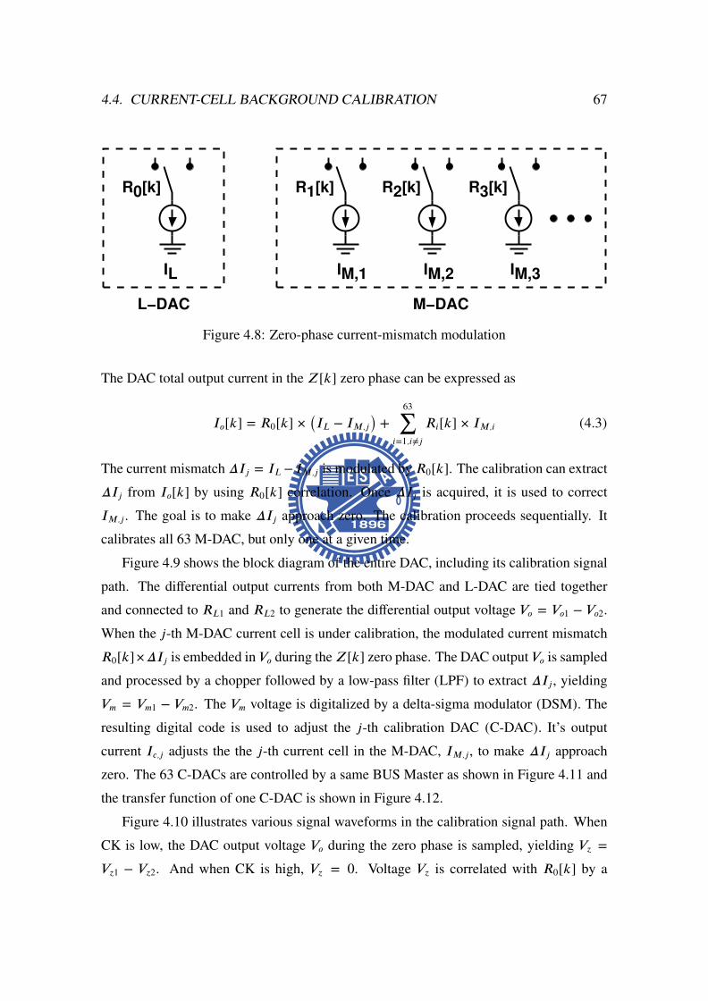
4.4. CURRENT-CELL BACKGROUND CALIBRATION 67
IL
0R
IM,1 IM,2 IM,3
1R 2R 3R[k] [k] [k] [k]
L−DAC M−DAC
Figure 4.8: Zero-phase current-mismatch modulation
The DAC total output current in the Z[k] zero phase can be expressed as
Io[k] = R0[k] ×(
IL − IM,j
)
+63∑
i=1,i 6=j
Ri[k] × IM,i (4.3)
The current mismatch ∆Ij = IL−IM,j is modulated by R0[k]. The calibration can extract
∆Ij from Io[k] by using R0[k] correlation. Once ∆Ij is acquired, it is used to correct
IM,j. The goal is to make ∆Ij approach zero. The calibration proceeds sequentially. It
calibrates all 63 M-DAC, but only one at a given time.
Figure 4.9 shows the block diagram of the entire DAC, including its calibration signal
path. The differential output currents from both M-DAC and L-DAC are tied together
and connected to RL1 and RL2 to generate the differential output voltage Vo = Vo1 − Vo2.
When the j-th M-DAC current cell is under calibration, the modulated current mismatch
R0[k]×∆Ij is embedded in Vo during theZ[k] zero phase. The DAC output Vo is sampled
and processed by a chopper followed by a low-pass filter (LPF) to extract ∆Ij, yielding
Vm = Vm1 − Vm2. The Vm voltage is digitalized by a delta-sigma modulator (DSM). The
resulting digital code is used to adjust the j-th calibration DAC (C-DAC). It’s output
current Ic,j adjusts the the j-th current cell in the M-DAC, IM,j, to make ∆Ij approach
zero. The 63 C-DACs are controlled by a same BUS Master as shown in Figure 4.11 and
the transfer function of one C-DAC is shown in Figure 4.12.
Figure 4.10 illustrates various signal waveforms in the calibration signal path. When
CK is low, the DAC output voltage Vo during the zero phase is sampled, yielding Vz =
Vz1 − Vz2. And when CK is high, Vz = 0. Voltage Vz is correlated with R0[k] by a
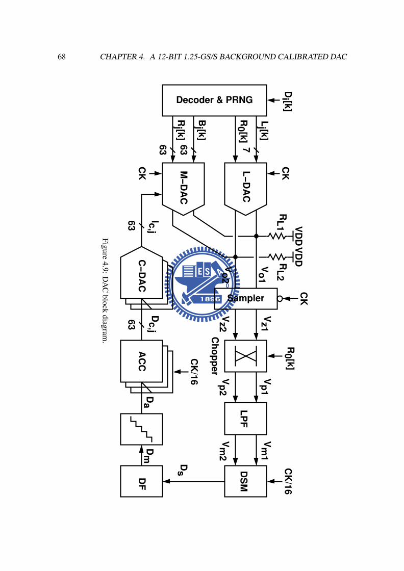
68 CHAPTER 4. A 12-BIT 1.25-GS/S BACKGROUND CALIBRATED DAC
L1R
L2RV
o1
Vo2
[k]R
0
Vp1
jR
[k]
Bj [k]
Lj [k][k]R
0
Dc,j
Dm
Ds
Di [k]
Ic,j
Vp2
Vz1
Vz2
Vm
2
Vm
1
Da
Sampler
CK
L−DA
CLP
FD
SM
CK
/16
M−D
AC
76363
Decoder & PRNG
CK
CK
C−D
AC
AC
C63
DF
Chopper
CK
/16
63 VD
DV
DD
Figure4.9:D
AC
blockdiagram
.
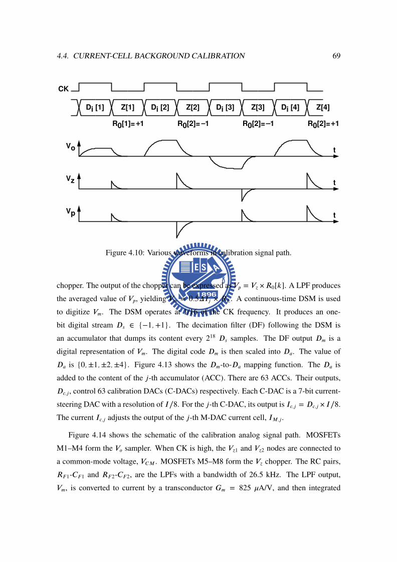
4.4. CURRENT-CELL BACKGROUND CALIBRATION 69
Di Di Di Di
Vo
Vz
Vp
R0 R0 R0R0
[1] [2] [3] [4]
11 1 1
CK
Z[2] Z[3] Z[4]Z[1]
[2]= [2]= [2]=[1]=
t
t
t
Figure 4.10: Various waveforms in calibration signal path.
chopper. The output of the chopper can be expressed as Vp = Vz×R0[k]. A LPF produces
the averaged value of Vp, yielding Vm = 0.5∆Ij × RL. A continuous-time DSM is used
to digitize Vm. The DSM operates at 1/16 of the CK frequency. It produces an one-
bit digital stream Ds ∈ −1,+1. The decimation filter (DF) following the DSM is
an accumulator that dumps its content every 218 Ds samples. The DF output Dm is a
digital representation of Vm. The digital code Dm is then scaled into Da. The value of
Da is 0,±1,±2,±4. Figure 4.13 shows the Dm-to-Da mapping function. The Da is
added to the content of the j-th accumulator (ACC). There are 63 ACCs. Their outputs,
Dc,j, control 63 calibration DACs (C-DACs) respectively. Each C-DAC is a 7-bit current-
steering DAC with a resolution of I/8. For the j-th C-DAC, its output is Ic,j = Dc,j×I/8.
The current Ic,j adjusts the output of the j-th M-DAC current cell, IM,j.
Figure 4.14 shows the schematic of the calibration analog signal path. MOSFETs
M1–M4 form the Vo sampler. When CK is high, the Vz1 and Vz2 nodes are connected to
a common-mode voltage, VCM . MOSFETs M5–M8 form the Vz chopper. The RC pairs,
RF1-CF1 and RF2-CF2, are the LPFs with a bandwidth of 26.5 kHz. The LPF output,
Vm, is converted to current by a transconductor Gm = 825 µA/V, and then integrated
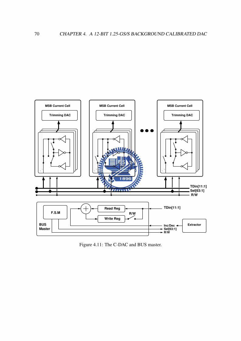
70 CHAPTER 4. A 12-BIT 1.25-GS/S BACKGROUND CALIBRATED DAC
MSB Current Cell
Trimming DAC
MSB Current Cell
Trimming DAC
MSB Current Cell
Trimming DAC
Write Reg
Read RegR/W
Sel[63:1]TDin[11:1]
R/W
Extractor
F.S.M
MasterBUS
TDin[11:1]
R/WSel[63:1]Inc/Dec
Figure 4.11: The C-DAC and BUS master.

4.4. CURRENT-CELL BACKGROUND CALIBRATION 71
TM7=
2LS
BTM
1=2L
SB
TL4=
1LS
BTL
3=0.
5LS
BTL
2=0.
25LS
BTL
1=0.
125L
SB
TDin
[11:
1]
Wri
te_B
us
TDin
[11:
1]
Wri
te[K
]
246810121416 016
3248
6480
9611
212
8TDin
Tout
(LS
B)
0.5L
SB
Mis
mat
ch <
0.5
LSB
TM7=
1.5L
SB
0.5L
SB
Loca
l Lat
ch &
Bus
_Sla
ve
Figu
re4.
12:T
heC
-DA
Can
dtr
ansf
erfu
nctio
n.
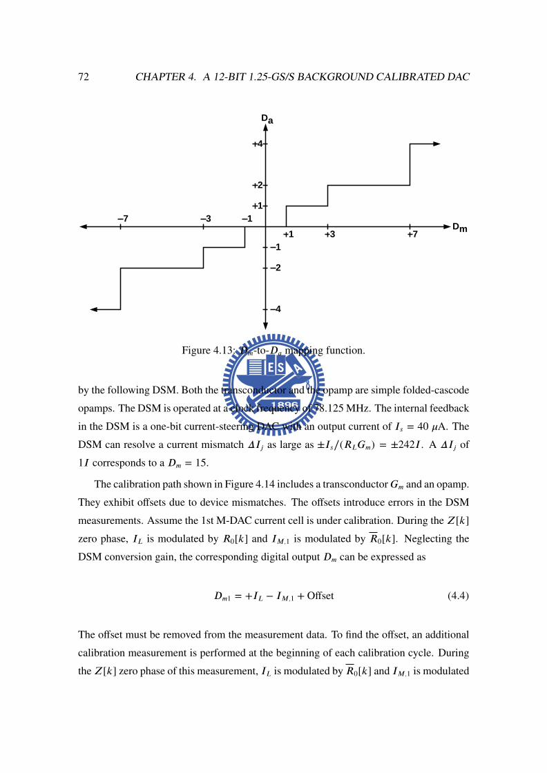
72 CHAPTER 4. A 12-BIT 1.25-GS/S BACKGROUND CALIBRATED DAC
Da
Dm
1
2
4
1
4
2
1 3 7
137
Figure 4.13: Dm-to-Da mapping function.
by the following DSM. Both the transconductor and the opamp are simple folded-cascode
opamps. The DSM is operated at a clock frequency of 78.125 MHz. The internal feedback
in the DSM is a one-bit current-steering DAC with an output current of Is = 40 µA. The
DSM can resolve a current mismatch ∆Ij as large as ±Is/(RLGm) = ±242I . A ∆Ij of
1I corresponds to a Dm = 15.
The calibration path shown in Figure 4.14 includes a transconductorGm and an opamp.
They exhibit offsets due to device mismatches. The offsets introduce errors in the DSM
measurements. Assume the 1st M-DAC current cell is under calibration. During the Z[k]
zero phase, IL is modulated by R0[k] and IM,1 is modulated by R0[k]. Neglecting the
DSM conversion gain, the corresponding digital output Dm can be expressed as
Dm1 = +IL − IM,1 + Offset (4.4)
The offset must be removed from the measurement data. To find the offset, an additional
calibration measurement is performed at the beginning of each calibration cycle. During
theZ[k] zero phase of this measurement, IL is modulated byR0[k] and IM,1 is modulated

4.4. CURRENT-CELL BACKGROUND CALIBRATION 73
CK
Vo1
Vo2
VC
M
VC
M
0R
[k]
0R
[k]
0R
[k]
Vp1
Vp2
F1R
F2R
mG
C1
C2
sD
I s
Vm
1
Vm
2
sD
Ω1
M
Ω1
MCF1
CF2
Vz1
Vz2
Low
−Pas
sFi
lter
CK
CK
M3
Sam
pler
M7
M8
Cho
pper
Del
ta−S
igm
a M
odul
ator
825
uA/V
S1
S2
40 u
A
CK
/16
6 pF
6 pF
M4
M1
M5
M2
M6 Fi
gure
4.14
:Sch
emat
icof
the
calib
ratio
nan
alog
sign
alpa
th.
74 CHAPTER 4. A 12-BIT 1.25-GS/S BACKGROUND CALIBRATED DAC
by R0[k]. The resulting digital output Dm can be expressed as
Dm2 = −IL + IM,1 + Offset (4.5)
Thus, the offset is obtained by applying (Dm1 + Dm2)/2. This acquired offset is sub-
tracted from the subsequent measurement data. Every calibration cycle includes one off-
set measurement and 63 mismatch measurements. The acquired offset is updated in every
calibration cycle.
As shown in Figure 4.10, due to the finite bandwidth of the Vo port, the sampled signal
Vz contains the return-to-zero tails of Vo. They are scrambled byR0[k] and reduced by the
following LPF and DF. The remaining residues cause calibration errors. The residues can
be reduced by increasing the DF down-sampling ratio. For this design, 218 consecutiveDs
data are accumulated for every Dm. This DF down-sampling ratio allows the worst-case
Vz, in which the sampled Vo holds its last data-phase value throughout the zero phase and
never decays.
With a DF down-sampling ratio of 218, one calibration measurement takes 3.34 msec.
Since one calibration cycle requires 64 measurements, it takes 214 msec to complete one
calibration cycle. During power up, it takes 9 calibration cycles or 1.93 sec for the calibra-
tion to converge if the initial M-DAC current cell mismatches are as large as 4.5I . After
that, the calibration only need to track the environmental variations, such as supply volt-
age and temperature variations. Although not implemented in this design, the calibration
time for the initial power up can be reduced by setting input Di[k] = 0 and then reducing
the DF down-sampling ratio.
The calibration technique collects mismatch from output signal, and the output wave-
form is not in a square shape due to the finite output port bandwidth. As shown in Fig-
ure 4.10, Vz is the sampled residue during zero phase. After the chopper, the residue is
moved to high frequency and mismatch information back to DC. In Figure 4.15, the high
frequency residue is the calibration noise should be eliminated by LPF and DF, and the
output port also cuts the shape of mismatch information. We define ηe as the collected
gain ratio of mismatch information in one clock period. Assume that the output port is
single pole dominated and ηe can be expressed in Equation (4.6).
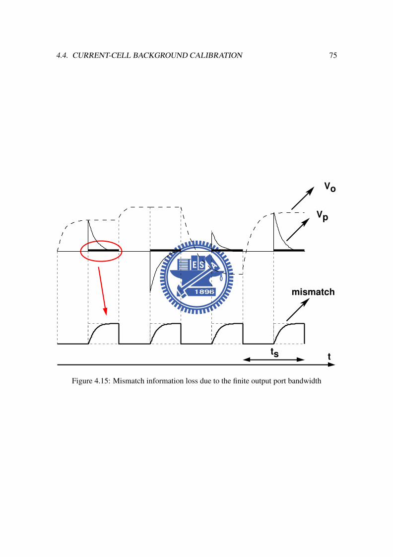
4.4. CURRENT-CELL BACKGROUND CALIBRATION 75
Vp
oV
ts t
mismatch
Figure 4.15: Mismatch information loss due to the finite output port bandwidth
76 CHAPTER 4. A 12-BIT 1.25-GS/S BACKGROUND CALIBRATED DAC
ηe =
∫ ts/20 RL(IL − IM,j)(1 − e−tτ )dt
RL(IL − IM,j) · ts=
ts2 + τe
−ts2τ − τts
(4.6)
where ts is the sampling clock and τ is the time constant of output pole. The calibration
noise is the zero phase residue which can be treated as RC discharging and the initial
voltage is the data phase signal, then the residue power ratio η in one clock period is
expressed as
η =
∫ ts/20
(
Vo(t) · e−tτ
)2dt
V 2o (t) · ts/2
=τ
ts(1 − e
−tsτ ) (4.7)
These two factors, ηe and η, are calculated in time domain; moreover, they can be
used in frequency domain. Assume that the output signal power spectrum density (PSD)
is So(f ), and the PSD of Vz is Sz(f ), the node shown in Figure 4.14. Vz is the Vo with
return-to-zero function and given by
Sz(f ) = So(f ) ·12sinc(
f
2fs) · η. (4.8)
The PSD of Vp is given by
Sp(f ) = Sz(f ) ∗ Sc(f ) (4.9)
where Sc(f ) is PSD of chopper signal which is a random binary sequence and given by
Sc(f ) =1
L2c
δ(f ) +1 + LcL2c
∞∑
n=−∞,n6=0
sinc2(n
Lc)δ(f −
n
Lcfs). (4.10)
In Equation (4.10), Lc is the period of the random sequence. Then, the high frequency
residue will be filtered by LPF and anti-alias filter of the DSM. Mismatch information
is moved back to DC, thus it’s mean can pass these two filters. The DSM and DF will
accumulate the power of filtered residue and the mean amplitude of mismatch information.
The in-band residue power denote as σ2n which is easy to find in frequency domain. The
decision equation is derived as
3 ·√
Mc · σn < Mc ·12· (I
8· RL · ηe) (4.11)
where Mc is the accumulation periods refer to DSM clock, 1/16 of the system clock, the
last term is the unit step of the calibration DAC through the calibration path. When output
signal Vo is low frequency, we need longer Mc to extract the mismatch.
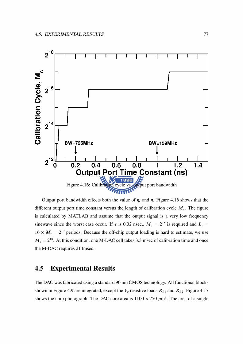
4.5. EXPERIMENTAL RESULTS 77
Figure 4.16: Calibration cycle vs. output port bandwidth
Output port bandwidth effects both the value of ηe and η. Figure 4.16 shows that the
different output port time constant versus the length of calibration cycle Mc. The figure
is calculated by MATLAB and assume that the output signal is a very low frequency
sinewave since the worst case occur. If τ is 0.32 nsec., Mc = 215 is required and Lc =
16 ×Mc = 219 periods. Because the off-chip output loading is hard to estimate, we use
Mc = 218. At this condition, one M-DAC cell takes 3.3 msec of calibration time and once
the M-DAC requires 214msec.
4.5 Experimental Results
The DAC was fabricated using a standard 90 nm CMOS technology. All functional blocks
shown in Figure 4.9 are integrated, except the Vo resistive loads RL1 and RL2. Figure 4.17
shows the chip photograph. The DAC core area is 1100 × 750 µm2. The area of a single

78 CHAPTER 4. A 12-BIT 1.25-GS/S BACKGROUND CALIBRATED DAC
Figure 4.17: Microphotograph of the DAC.
4.5. EXPERIMENTAL RESULTS 79
M-DAC current cell is 90 × 12 µm2. The chip also includes a direct digital frequency
synthesizer (DDFS) to generate digital inputs for DAC dynamic testing. The synthesizer
can also generates ramp waveforms for DNL and INL measurements.
The measured DNL and INL before calibration is shown in Figure 4.18. In our design,
the device dimensions and bias conditions for the L-DAC current cells are different from
those for the M-DAC current cells. In addition, this DAC floor plan does not employ
common-centroid scheme to reduce the gradient effects. As a result, the raw DNL and
INL are poor. The DNL is +4.5/−0.5 LSB and the INL is +10.2/−7.1 LSB. Figure 4.18
shows the measured DNL and INL after current-cell calibration. The DNL is improved
up to +0.47/−0.51 LSB and the INL is improved up to +1.0/−1.2 LSB.
Figure 4.20 shows the measured DAC full-scale transient response. The 10%-to-90%
rising time is 0.5 nsec, which corresponds to an output-port bandwidth of 700 MHz. For
this DAC, the DRRZ operation is applied to its differential output current Io. Its differen-
tial output voltage Vo may not return to zero due to the finite output-port bandwidth. Both
the DRRZ and the current-cell background calibration can operate and be effective under
any output-port bandwidth. They put no restriction on choosing output-port bandwidth.
The DAC output spectra are measured during the single-tone tests. The DAC is oper-
ated at 1.25 GS/s sampling rate. shows the output spectrum of the DAC without calibration
and DRRZ. The spectrum is spurious with the 2nd, 3rd and 5th order distortions which
are cause by the static linearity. We measured the output voltage of each digital input and
then use MATLAB to run a FFT test shown in Figure 4.25. This the first step to check
if the measurement environment for dynamic test is ready. Figure 4.22 shows the output
spectrum when the input frequency is 40 MHz. The DAC is calibrated and the DRRZ is
turned off. The SFDR is 73.3 dB. At low input frequencies, the CDST effect is low. The
SFDR is dictated by the DAC static linearity. In this design, the static linearity is achieved
by calibration. Figure 4.23 shows the DAC output spectrum with the input frequency in-
creased to 477 MHz. The SFDR is degraded to 58.8 dB by the CDST effect. Figure 4.24
shows the DAC output spectrum with the DRRZ enabled. The SFDR recovers to 73.6 dB.
The DRRZ mitigates the CDST effect.
Several sources contribute the random noises at DAC output. They are estimated as
follows. (1) The total quantization noise power is I2n1 = I2/12. Assume the signal band-

80 CHAPTER 4. A 12-BIT 1.25-GS/S BACKGROUND CALIBRATED DAC
Figure 4.18: Measured DNL and INL before current-cell calibration.
Figure 4.19: Measured DNL and INL after current-cell calibration.
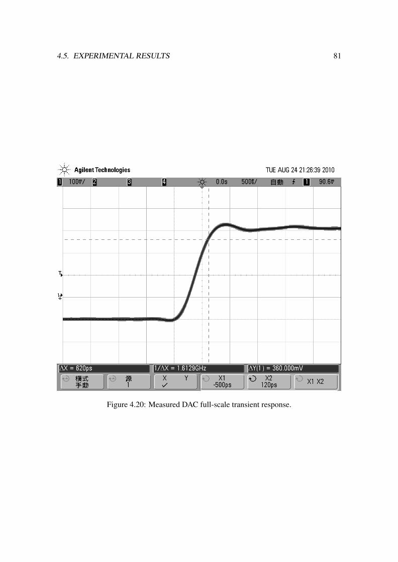
4.5. EXPERIMENTAL RESULTS 81
Figure 4.20: Measured DAC full-scale transient response.
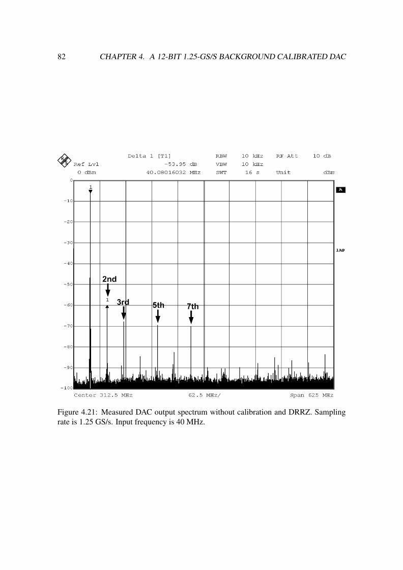
82 CHAPTER 4. A 12-BIT 1.25-GS/S BACKGROUND CALIBRATED DAC
Figure 4.21: Measured DAC output spectrum without calibration and DRRZ. Samplingrate is 1.25 GS/s. Input frequency is 40 MHz.
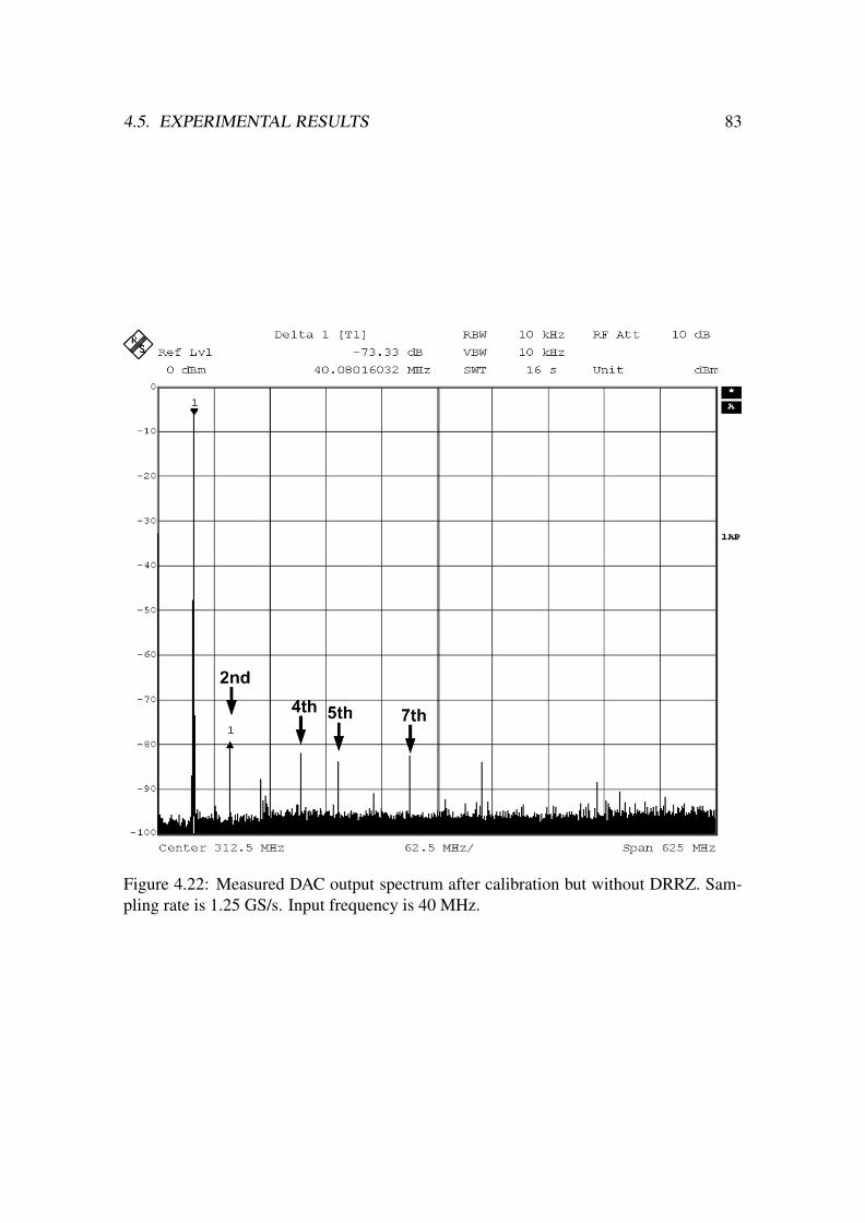
4.5. EXPERIMENTAL RESULTS 83
Figure 4.22: Measured DAC output spectrum after calibration but without DRRZ. Sam-pling rate is 1.25 GS/s. Input frequency is 40 MHz.

84 CHAPTER 4. A 12-BIT 1.25-GS/S BACKGROUND CALIBRATED DAC
Figure 4.23: Measured DAC output spectrum after calibration but without DRRZ. Sam-pling rate is 1.25 GS/s. Input frequency is 477 MHz.
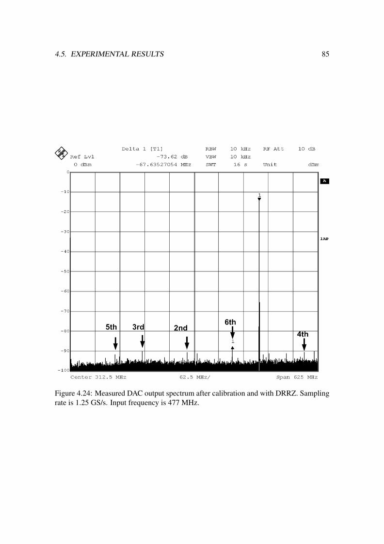
4.5. EXPERIMENTAL RESULTS 85
Figure 4.24: Measured DAC output spectrum after calibration and with DRRZ. Samplingrate is 1.25 GS/s. Input frequency is 477 MHz.
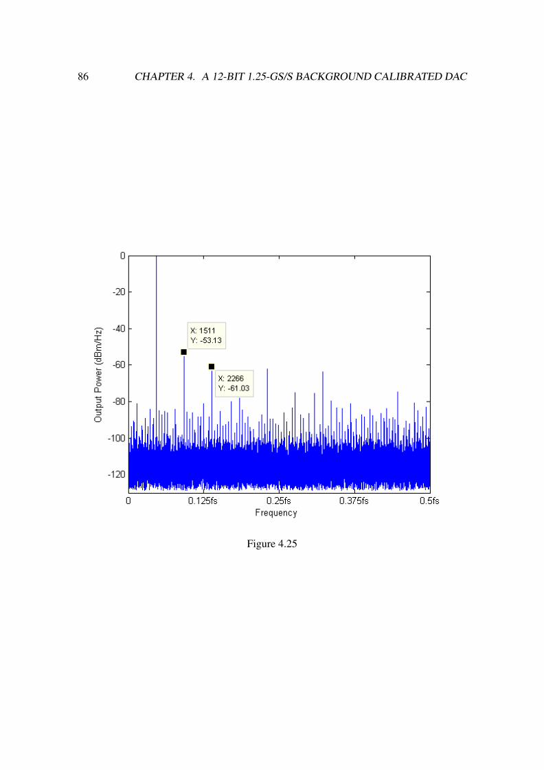
86 CHAPTER 4. A 12-BIT 1.25-GS/S BACKGROUND CALIBRATED DAC
Figure 4.25

4.5. EXPERIMENTAL RESULTS 87
Figure 4.26: Measured SFDR versus input frequencies
width is 625 MHz. The current power density is I2n1/∆f = 2.13×10⁻²¹ A2/Hz. The corre-
sponding noise spectral density (NSD) received by the SA is NSD1 = −165.74 dBm/Hz.
(2) The current sources in the DAC contain device thermal noises. From simulation,
the total DAC output current density due to these thermal noises is I2n2/∆f = 2.05 ×
10−21 A2/Hz. The corresponding NSD received by the SA is NPD2 = −171.93 dBm/Hz.
(3) Comparing Figure 4.23 to Figure 4.22, the power increase in the harmonics is ∆Pst =
10−7 mW as input frequency is increased. Assume ∆Pst is induced entirely by the CDST
effect, and it is spread from 0 Hz to fs/2 by the DRRZ. The resulting NSD is NSD3 =
∆Pst/(fs/2) = −158 dBm/Hz. The SA in our measurement setup has a noise floor of
−140 dBm/Hz by itself. It is too high for the SA to measure the DAC output noises
directly.
Figure 4.26 shows the measured SFDR versus input frequencies. If the DAC is not

88 CHAPTER 4. A 12-BIT 1.25-GS/S BACKGROUND CALIBRATED DAC
Figure 4.27: Measured SNDR versus input frequencies. The SNDR of the DAC is limitedby the Signal Analyzer
calibrated, the SFDR exhibits no significant change by varying input frequency. The DAC
static linearity dominates the SFDR performance. Once the DAC is calibrated, and if the
DRRZ is turned off, the CDST effect is the main source of SFDR degradation. When the
DAC is calibrated and the DRRZ is turned on, the SFDR is better than 70 dB for input
frequencies up to 500 MHz. Also shown in Figure 4.26 is the CDLV effect calculated
with Equation (4.1). In this design, the CDLV effect becomes relevant only when the
input frequency is higher than 550 MHz.
Table 4.2 summarizes the DAC specifications. Figure 4.28 compares the SFDR per-
formances of several high-speed DAC published in recent years. Our design has the best
dynamic performance.
Figure 4.28 compares the SFDR performance of several high-speed DAC of which the
sampling rate is higher than 0.5 GS/s and the resolution is better than 12 bits. Table 4.3
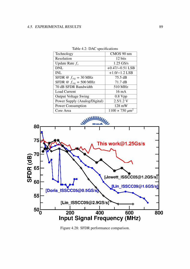
4.5. EXPERIMENTAL RESULTS 89
Table 4.2: DAC specificationsTechnology CMOS 90 nmResolution 12 bitsUpdate Rate fs 1.25 GS/sDNL +0.47/−0.51 LSBINL +1.0/−1.2 LSBSFDR @ fsig = 30 MHz 75.5 dBSFDR @ fsig = 500 MHz 71.7 dB70 dB SFDR Bandwidth 510 MHzLoad Current 16 mAOutput Voltage Swing 0.8 VppPower Supply (Analog/Digital) 2.5/1.2 VPower Consumption 128 mWCore Area 1100 × 750 µm2
Figure 4.28: SFDR performance comparison.
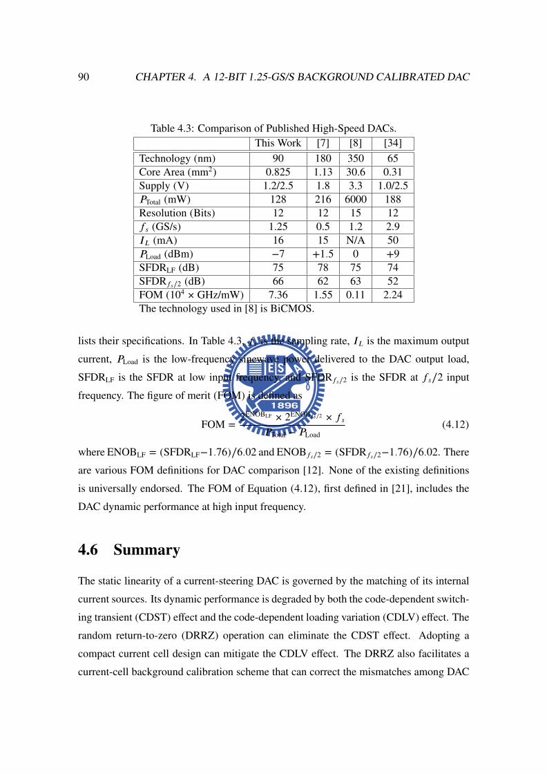
90 CHAPTER 4. A 12-BIT 1.25-GS/S BACKGROUND CALIBRATED DAC
Table 4.3: Comparison of Published High-Speed DACs.This Work [7] [8] [34]
Technology (nm) 90 180 350 65Core Area (mm2) 0.825 1.13 30.6 0.31Supply (V) 1.2/2.5 1.8 3.3 1.0/2.5PTotal (mW) 128 216 6000 188Resolution (Bits) 12 12 15 12fs (GS/s) 1.25 0.5 1.2 2.9IL (mA) 16 15 N/A 50PLoad (dBm) −7 +1.5 0 +9SFDRLF (dB) 75 78 75 74SFDRfs/2 (dB) 66 62 63 52FOM (104 × GHz/mW) 7.36 1.55 0.11 2.24The technology used in [8] is BiCMOS.
lists their specifications. In Table 4.3, fs is the sampling rate, IL is the maximum output
current, PLoad is the low-frequency sinewave power delivered to the DAC output load,
SFDRLF is the SFDR at low input frequency, and SFDRfs/2 is the SFDR at fs/2 input
frequency. The figure of merit (FOM) is defined as
FOM =2ENOBLF × 2ENOBfs/2 × fs
PTotal − PLoad(4.12)
where ENOBLF = (SFDRLF−1.76)/6.02 and ENOBfs/2 = (SFDRfs/2−1.76)/6.02. There
are various FOM definitions for DAC comparison [12]. None of the existing definitions
is universally endorsed. The FOM of Equation (4.12), first defined in [21], includes the
DAC dynamic performance at high input frequency.
4.6 Summary
The static linearity of a current-steering DAC is governed by the matching of its internal
current sources. Its dynamic performance is degraded by both the code-dependent switch-
ing transient (CDST) effect and the code-dependent loading variation (CDLV) effect. The
random return-to-zero (DRRZ) operation can eliminate the CDST effect. Adopting a
compact current cell design can mitigate the CDLV effect. The DRRZ also facilitates a
current-cell background calibration scheme that can correct the mismatches among DAC

4.6. SUMMARY 91
internal current sources due to device variations. We designed a CMOS 12-bit 1.25-GS/s
current-steering DAC to demonstrate the above design techniques. As a result, the DAC
achieves a SFDR better than 70 dB up to 500 MHz input frequency.

92 CHAPTER 4. A 12-BIT 1.25-GS/S BACKGROUND CALIBRATED DAC

Chapter 5
Conclusions and Future Works
5.1 Conclusions
High-speed and high-performance DACs require large signal bandwidth and low switch-
ing noise. In this thesis, we proposed background calibration which allows the use of
small size current cells. Then, the signal bandwidth can extend. The DAC is insensitive
to the PVT variations and slow time-variant error. We also proposed a Digital Random
Return-to-Zero to randomize the code-dependant switching transients rather than elimate
the transients. The switching transients contribute to harmonic distortions and would
damage the adjcent channel. The DRRZ technique relax the spur-expression requirement
of reconstruction filter. Moreover, the induced noise power is spread into all the Nyquist
band, and only a portion of noise into the channel power.
Finally, all the experimental Results were verified by these two high-speed DACs. The
results show the theory was truth and can be implemented in silicon. The 8-bit 1.6-GS/s
current-steering DAC shows an 14 dB improvement in SFDR when the input frequency is
800 MHz. The 12-bit 1.25-GS/s current-steering DAC achieves a SFDR better than 70 dB
up to 500 MHz input frequency.
93
94 CHAPTER 5. CONCLUSIONS AND FUTURE WORKS
5.2 Recommendations for Future Investigation
This section presents several suggestions for future investigations for these high-speed
and high-resolution DACs.
• To develop technique to improve the output power efficiency. The RZ output loss
6 dB signal power; however, anti-droop filter can be avoided in RZ DACs.
• To analysis the additional noise power caused by DRRZ.
• The CAL-DAC design optimization is needed. The mismatch information of the M-
DAC cells are saved in local latch which occupied large area. Also the CAL-DAC
can be implemented in more low cost way.

Bibliography
[1] B. Schafferer and R. Adams, “A 3V CMOS 400mW 14b 1.4GS/s DAC for multi-
carrier applications,” in IEEE International Solid-State Circuits Conference Digest
of Technical Papers, Feb. 2004, pp. 360–362.
[2] C.-H. Lin and K. Bult, “A 10-b, 500-MSample/s CMOS DAC in 0.6 mm2,” IEEE J.
Solid-State Circuits, vol. 33, no. 12, pp. 1948 –1958, Dec. 1998.
[3] N. Ghittori, A. Vigna, P. Malcovati, S. D’Amico, and A. Baschirotto, “1.2-
V low-power multi-mode DAC+Filter blocks for reconfigurable (WLAN/UMTS,
WLAN/Bluetooth) transmitters,” IEEE J. Solid-State Circuits, vol. 41, no. 9, pp.
1970 –1982, Sep. 2006.
[4] M.-J. Choe, K.-H. Baek, and M. Teshome, “A 1.6-GS/s 12-bit return-to-zero GaAs
RF DAC for multiple nyquist operation,” IEEE J. Solid-State Circuits, vol. 40,
no. 12, pp. 2456 – 2468, Dec. 2005.
[5] J. Hyde, T. Humes, C. Diorio, M. Thomas, and M. Figueroa, “A 300-MS/s 14-bit
digital-to-analog converter in logic CMOS,” IEEE J. Solid-State Circuits, vol. 38,
no. 5, pp. 734–740, May 2003.
[6] A. van den Bosch, M. Borremans, M. Steyaert, and W. Sansen, “A 10-bit 1-
GSample/s nyquist current-steering CMOS D/A converter,” IEEE J. Solid-State Cir-
cuits, vol. 36, no. 3, pp. 315 –324, Mar. 2001.
[7] K. Doris, J. Briaire, D. Leenaerts, M. Vertregt, and A. van Roermund, “A 12b
500MS/s DAC with >70dB SFDR up to 120MHz in 0.18mum CMOS,” in IEEE
International Solid-State Circuits Conference Digest of Technical Papers, Feb. 2005.
95
96 BIBLIOGRAPHY
[8] B. Jewett, J. Liu, and K. Poulton, “A 1.2GS/s 15b DAC for precision signal gen-
eration,” in IEEE International Solid-State Circuits Conference Digest of Technical
Papers, Feb. 2005, pp. 110–112.
[9] K. Gulati, M. Peng, A. Pulincherry, C. Munoz, M. Lugin, A. Bugeja, J. Li, and
A. Chandrakasan, “A highly integrated CMOS analog baseband transceiver with
180 MSPS 13-bit pipelined CMOS ADC and dual 12-bit DACs,” IEEE J. Solid-State
Circuits, vol. 41, no. 8, pp. 1856 –1866, Aug. 2006.
[10] X. Wu, P. Palmers, and M. S. J. Steyaert, “A 130 nm CMOS 6-bit full nyquist 3 GS/s
DAC,” IEEE J. Solid-State Circuits, vol. 43, pp. 2396–2403, Nov. 2008.
[11] C.-H. Lin, F. M. L. van der Goes, J. R. Westra, J. Mulder, Y. Lin, E. Arslan,
E. Ayranci, X. Liu, and K. Bult, “A 12 bit 2.9 GS/s DAC with IM3 < -60dBc be-
yond 1 GHz in 65nm CMOS,” IEEE J. Solid-State Circuits, vol. 44, no. 12, pp.
3285–3293, Dec. 2009.
[12] P. Palmers and M. S. J. Steyaert, “A 10-bit 1.6-GS/s 27-mw current-steering D/A
converter with 550-Mhz 54-db SFDR bandwidth in 130-nm CMOS,” IEEE Trans.
Circuits Syst. I, vol. 57, no. 11, pp. 2870–2879, Nov. 2010.
[13] M. Pelgrom, A. Duinmaijer, and A. Welbers, “Matching properties of MOS transis-
tors,” IEEE J. Solid-State Circuits, vol. 24, no. 5, pp. 1433–1439, Oct. 1989.
[14] D. Groeneveld, H. Schouwenaars, H. Termeer, and C. Bastiaansen, “A self-
calibration technique for monolithic high-resolution D/A converters,” IEEE J. Solid-
State Circuits, vol. 24, no. 6, pp. 1517 –1522, Dec. 1989.
[15] A. R. Bugeja and B.-S. Song, “A self-trimming 14-b 100-MS/s CMOS DAC,” IEEE
J. Solid-State Circuits, vol. 35, no. 12, pp. 1841–1852, Dec. 2000.
[16] M. Tiilikainen, “A 14-bit 1.8-v 20-mw 1-mm2 CMOS DAC,” IEEE J. Solid-State
Circuits, vol. 36, no. 7, pp. 1144 –1147, Jul. 2001.
BIBLIOGRAPHY 97
[17] Y. Cong and R. L. Geiger, “A 1.5v 14b 100MS/s self-calibrated DAC,” in IEEE
International Solid-State Circuits Conference Digest of Technical Papers, Feb. 2003,
pp. 128–130.
[18] Q. Huang, P. A. Francese, C. Martelli, and J. Nielsen, “A 200MS/s 14b 97mW DAC
in 0.18µm CMOS,” in IEEE International Solid-State Circuits Conference Digest of
Technical Papers, Feb. 2004.
[19] H.-H. Chen, J. Lee, J. Weiner, Y.-K. Chen, and J.-T. Chen, “A 14-b 150 MS/s CMOS
DAC with digital background calibration,” in VLSI Circuits, 2006. Digest of Techni-
cal Papers. 2006 Symposium on, 2006.
[20] D. Mercer, “Low-power approaches to high-speed current-steering digital-to-analog
converters in 0.18-µm CMOS,” IEEE J. Solid-State Circuits, vol. 42, no. 8, pp. 1688
–1698, Aug. 2007.
[21] M. Clara, W. Klatzer, B. Seger, A. Di Giandomenico, and L. Gori, “A 1.5V
200MS/s 13b 25mW DAC with randomized nested background calibration in 0.13
µm CMOS,” in IEEE International Solid-State Circuits Conference Digest of Tech-
nical Papers, Feb. 2007, pp. 250 –600.
[22] D.-L. Shen, Y.-C. Lai, and T.-C. Lee, “A 10-bit binary-weighted DAC with digital
background LMS calibration,” in Solid-State Circuits Conference, 2007. ASSCC ’07.
IEEE Asian, Nov. 2007, pp. 352 –355.
[23] J.-H. Chi, S.-H. Chu, and T.-H. Tsai, “A 1.8-V 12-bit 250-MS/s 25-mW self-
calibrated DAC,” in ESSCIRC, 2010 Proceedings of the, Sep. 2010, pp. 222 –225.
[24] K. L. Chan, J. Zhu, and I. Galton, “Dynamic element matching to prevent nonlinear
distortion from pulse-shape mismatches in high-resolution DACs,” IEEE J. Solid-
State Circuits, vol. 43, no. 9, pp. 2607–2078, Sep. 2008.
[25] H. Jensen and I. Galton, “An analysis of the partial randomization dynamic element
matching technique,” Circuits and Systems II: Analog and Digital Signal Processing,
IEEE Transactions on, vol. 45, no. 12, pp. 1538 –1549, Dec. 1998.

98 BIBLIOGRAPHY
[26] J. Welz and I. Galton, “Necessary and sufficient conditions for mismatch shaping
in a general class of multibit DACs,” Circuits and Systems II: Analog and Digital
Signal Processing, IEEE Transactions on, vol. 49, no. 12, pp. 748 – 759, Dec. 2002.
[27] D.-H. Lee, Y.-H. Lin, and T.-H. Kuo, “Nyquist-rate current-steering digital-to-
analog converters with random multiple data-weighted averaging technique and ro-
tated walk switching scheme,” Circuits and Systems II: Express Briefs, IEEE Trans-
actions on, vol. 53, no. 11, pp. 1264 –1268, Nov. 2006.
[28] M.-H. Shen, J.-H. Tsai, and P.-C. Huang, “Random swapping dynamic element
matching technique for glitch energy minimization in current-steering DAC,” IEEE
Trans. Circuits Syst. II, vol. 57, no. 5, pp. 1433–1439, May 2010.
[29] R. Radke, A. Eshraghi, and T. Fiez, “A spurious-free delta-sigma DAC using rotated
data weighted averaging,” in Custom Integrated Circuits, 1999. Proceedings of the
IEEE 1999, 1999.
[30] G. Van Der Plas, J. Vandenbussche, W. Sansen, M. Steyaert, and G. Gielen, “A 14-
bit intrinsic accuracy q2 random walk CMOS DAC,” IEEE J. Solid-State Circuits,
vol. 34, no. 12, pp. 1708 –1718, Dec. 1999.
[31] A. R. Bugeja, B.-S. Song, P. L. Rakers, and S. F. Gillig, “A 14-b, 100-MS/s CMOS
DAC designed for spectral performance,” IEEE J. Solid-State Circuits, vol. 34,
no. 12, pp. 1719–1732, Dec. 1999.
[32] W.-H. Tseng, J.-T. Wu, and Y.-C. Chu, “A CMOS 8-bit 1.6-GS/s DAC with digital
random return-to-zero,” IEEE Trans. Circuits Syst. II, vol. 58, no. 1, pp. 1–5, Jan.
2011.
[33] J. Deveugele and M. Steyaert, “A 10b 250MS/s binary-weighted current-steering
DAC,” in IEEE International Solid-State Circuits Conference Digest of Technical
Papers, Feb. 2004, pp. 362–364.
[34] C.-H. Lin, F. M. L. van der Goes, J. R. Westra, J. Mulder, Y. Lin, E. Arslan,
E. Ayranci, X. Liu, and K. Bult, “A 12 bit 2.9 GS/s DAC with IM3 < -60dBc be-

BIBLIOGRAPHY 99
yond 1 GHz in 65nm CMOS,” IEEE J. Solid-State Circuits, vol. 44, no. 12, pp.
3285–3293, Dec. 2009.
[35] W.-H. Tseng, C.-W. Fan, and J.-T. Wu, “A 12b 1.25GS/s DAC in 90nm CMOS with
>70db SFDR up to 500MHz,” in IEEE International Solid-State Circuits Conference
Digest of Technical Papers, Feb. 2011, pp. 192–193.
[36] H. Jiang, D. Chen, and R. Geiger, “Deterministic DEM DAC performance analysis,”
in Circuits and Systems, 2007. ISCAS 2007. IEEE International Symposium on, May
2007, pp. 3860 –3863.
[37] K. L. Chan, J. Zhu, and I. Galton, “A 150MS/s 14-bit segmented DEM DAC with
greater than 83dB of SFDR across the Nyquilst band,” in VLSI Circuits, 2007 IEEE
Symposium on, Jun. 2007, pp. 200 –201.
[38] T. Chen and G. G. E. Gielen, “The analysis and improvement of a current-steering
DACs dynamic SFDR–I: The cell-dependent delay differences,” IEEE Trans. Cir-
cuits Syst. I, vol. 53, no. 1, pp. 3–15, Jan. 2006.
[39] K. Andersson and M. Vesterbacka, “Modeling of glitches due to rise/fall asymme-
try in current-steering digital-to-analog converters,” Circuits and Systems I: Regular
Papers, IEEE Transactions on, vol. 52, no. 11, pp. 2265 – 2275, Nov. 2005.
[40] J. Bastos, A. Marques, M. Steyaert, and W. Sansen, “A 12-bit intrinsic accuracy
high-speed CMOS DAC,” IEEE J. Solid-State Circuits, vol. 33, no. 12, pp. 1959
–1969, Dec. 1998.
[41] W. Schofield, D. Mercer, and L. Onge, “A 16b 400MS/s dac with <-80dBc IMD
to 300mhz and <-160dBm/Hz noise power spectral density,” in IEEE International
Solid-State Circuits Conference Digest of Technical Papers, Feb. 2003, pp. 126 –
482 vol.1.
[42] A. V. den Bosch, M. Steyaert, and W. Sansen, “SFDR-bandwidth limitations for
high-speed high-resolution current-steering CMOS D/A converters,” Proc. IEEE
Int. Conf. Electronics, Circuits and Systems (ICECS), pp. 1193–1196, Sep. 1999.
100 BIBLIOGRAPHY
[43] S. Luschas and H.-S. Lee, “Output impedance requirements for DACs,” in IEEE
International Symposium on Circuits and Systems Digest of Technical Papers, May
2003.
[44] B. Razavi, Principles of Data Conversion System Design. IEEE Press, 1995, no.
ISBN 0-7803-1093-4.
[45] S. Park, G. Kim, S.-C. Park, and W. Kim, “A digital-to-analog converter based on
differential-quad switching,” IEEE J. Solid-State Circuits, vol. 37, no. 10, pp. 1335–
1338, Oct. 2002.

F
Wei-Hsin received the B.S. degree from the department of electrical engineering, National
Cheng Kung University(NCKU), Tainan, Taiwan, R.O.C., in 2002. From 2002 to 2011,
he worked toward the M.S. and Ph.D. degree in electronics engineering with the National
Chiao-Tung University, Hsinchu. His current research interest is high-speed high- resolu-
tion data converters design.
In 2010, he joined the MediaTek where he was engaged in the design of analog and
mixed-signal ICs.
ë: R;¨¨)D 166r
Í¡Z¸à LATEX1 Ù4Ì.
1LATEX Î TEX ìÝ macros /. TEX Î American Mathematical Society ÝÛ¤ý. Í¡ZmacrosÝæ®ïÎ Dinesh Das, Department of Computer Sciences, The University of Texas at Austin.øZÌÝ®ïÎÒ+/,ø;.é.,±z,¬È.
101
Publication List• Journal Paper:
– W.-H. Tseng, J.-T. Wu, and Y.-C. Chu,E A CMOS 8-bit 1.6-GS/s DAC with
digital random return-to-zero,F IEEE Trans. Circuits Syst. II, vol. 58, no. 1,
pp. 1 5, Jan. 2011.
– W.-H. Tseng, C.-W. Fan, and J.-T. Wu,E A 12-Bit 1.25-GS/s DAC in 90nm
CMOS with > 70dB SFDR up to 500MHz,F Submitted to the invited Special
Issue of ISSCC.
• Conference Paper:
– W.-H. Tseng, C.-W. Fan, and J.-T. Wu,E A 12-Bit 1.25-GS/s DAC in 90nm
CMOS with > 70dB SFDR up to 500MHz,F in IEEE International Solid-
State Circuits Conference Digest of Technical Papers, Feb. 2011, pp. 192
193.