studies on wo 3 thin films prepared by dip-coating...
TRANSCRIPT

STUDIA UNIVERSITATIS BABE -BOLYAI, CHEMIA, LIV, 3, 2009
STUDIES ON WO3 THIN FILMS PREPARED BY DIP-COATING METHOD
ECATERINA BICAa,b, LAURA ELENA MURE ANa, LUCIAN BARBU-TUDORANc, EMIL INDREAd, IONEL C T LIN POPESCUb AND
ELISABETH-JEANNE POPOVICIa
ABSTRACT. WO3 films obtained by dip-coating technique were investigated to evidence the properties of tungsten trioxide films for water splitting applications. The deposition solution containing peroxo-tungstic acid was prepared by sol-gel method. The films were deposited on conductive glass substrates and were annealed at 250-550
0C. The properties of WO3 films were investigated
by UV-Vis Spectroscopy, X-Ray diffraction (XRD) and Scanning Electron Microscopy (SEM).
Keywords: Tungsten trioxide films; ITO support; Dip-coating.
INTRODUCTION
Tungsten oxide (WO3) is a wide – band gap semiconductor of great interest because of its applications in optoelectronics, catalysis and environmental engineering [1-3]. On the other hand, it was demonstrated that WO3 thin films exhibits chemical sensing properties such as H2S, NOx, [4-7]. Moreover, WO3 thin films electrodes are reversible and have fast electrochromic properties [8].
Tungsten oxide films can be synthesized by several physical and chemical routes such as sputtering [9], acid precipitation method [10] and sol-gel processing [11-14].
Application of tungsten trioxide (WO3) thin films strongly depends on morpho-structural characteristics that are regulated during the synthesis.
The aim of this study is to obtain high quality WO3 thin films for photo-catalysis and water splitting applications. The performed study presents the influence of some preparative conditions on the morpho-structural characteristics
a Babe -Bolyai University, “Raluca Ripan” Institute for Research in Chemistry, Fantanele 30,
Cluj-Napoca, Romania, [email protected] b Babe -Bolyai University, Faculty of Chemistry and Chemical Engineering, Arany Janos 11,
Cluj-Napoca, Romania c Babe -Bolyai University, Electronic Microscopy Centre, Clinicilor 5-7, Cluj-Napoca, Romania
d National Institute for R&D of Isotopic and Molecular Technologies, Donath 30, Cluj-Napoca,
Romania
E. BICA, L.E. MURE AN, L. BARBU-TUDORAN, E. INDREA, I.C. POPESCU, E.-J. POPOVICI
16
of WO3 films, and put in evidence that the quality of the dip-coating solution and the thermal treatment play an important role on the properties of conductive glass supported WO3 films. RESULTS AND DISCUSSIONS
WO3/ITO/Glass/WO3 heterostructures containing tungsten oxide thin films were obtained using the dip-coating method, from peroxo-tungstic acid sol. The multilayer technique was used to prepare films with variable thickness
whereas the thermal treatment was performed at 250 - 550 C (Table 1).
Film thickness varies between 35 and 135 nm, in parallel with the number of dip coating deposition cycles; it seems that the thickness is not influenced by the annealing regime.
Table 1. Synthesis conditions of WO3 thin films prepared from
peroxo-tungstic acid sol (dip-coating method)
Sample code Thermal treatment
(0C)
Number of layers
WO3 weight (g)
Film thickness (nm)
R4 I1 350 1 0.55 x 10⁻³
35
R4 I2 350 2 0.94 x 10⁻³
60
R4 I3 350 3 1.62 x 10⁻³
95
R4 I4 350 4 1.97 x 10⁻³
125
R4 I5 350 5 2.20x 10⁻³
135
R3.1 I2 250 1 0.30 x 10⁻³
20
R3.1 I3 350 1 0.56 x 10⁻³
35
R3.1 I4 550 1 0.50 x 10⁻³
35
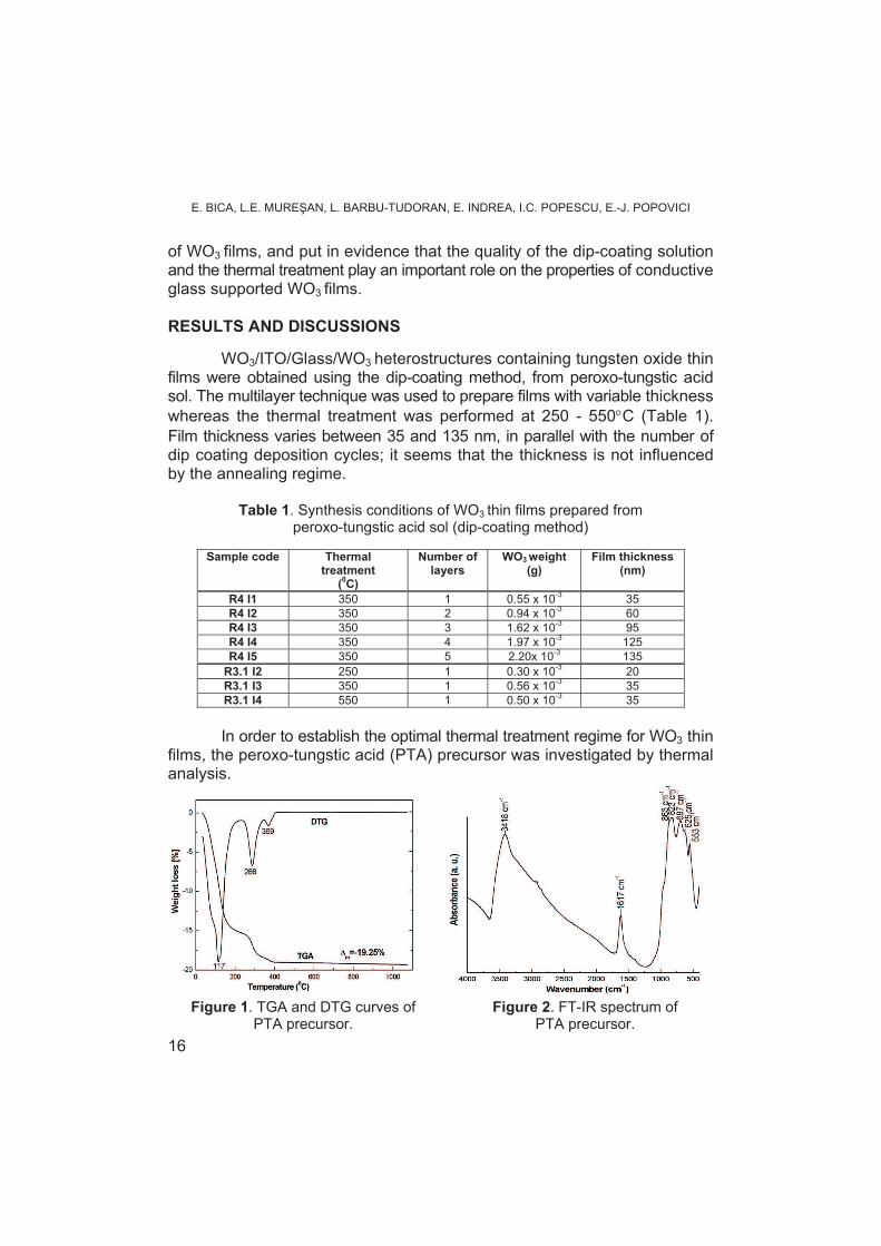
In order to establish the optimal thermal treatment regime for WO3 thin
films, the peroxo-tungstic acid (PTA) precursor was investigated by thermal analysis.
Figure 1. TGA and DTG curves of
PTA precursor. Figure 2. FT-IR spectrum of
PTA precursor.

STUDIES ON WO3 THIN FILMS PREPARED BY DIP-COATING METHOD
17
The TGA and DTG curves of PTA precursor indicate three most
important weight loss steps i.e. (1) -14.92% at 20-200 C (removal of physical
adsorbed water and alcohol); (2) -3.35% at 235-345 C (removal of H2O2, i.e.
peroxo-tungstic acid decomposition) and (3) -1.05% at 345-405 C (removal of
chemically bonded water i.e. tungstic acid decomposition) (Fig.1).The weight loss steps are accompanied by weak endo- and exo- thermal effects.
The FT-IR spectrum of the precursor powder (that corresponds to the as- deposited WO3 film), illustrates the hydrated and the hydroxilated nature of the WO3 deposit (Figure 2). Water presence is signalled by the
3418 cm-1 { (OH)} and 1617 cm-1 { (HOH)} bands. Because the (OH) appears
as a single featureless band, it is difficult to isolate the independent contributions from structural water, hydroxyl groups, hydrogen bonded and adsorbed species. Despite the complexity of the W-O stretching bands region (400-1000cm-1), it
gives important information about the precursor. Besides the specific (W-Ointra-W)
and (W-Ointer-W) bridging stretches ( 863-823 cm-1 and 687 -625 cm-1), the
stretching vibrations of W(O2) and W-O could be noticed (959 cm-1 and 553 cm-1), thus indicating the formation of [(O2)2W(O).O.W(O)(O2)2]2- complex associated with the peroxo-tungstic acid [15-17].
The optical properties of WO3 films were evaluated from UV-Vis transmission (Figure 3) and reflection (Figure 4) spectra.
a. b.
Figure 3. Transmission spectra of WO3 films obtained in different conditions:
a) multilayer films treated at 350 C; b) monolayer films annealed at 250 – 550 C.
The monolayer WO3 film (R4I1) shows an almost constant transmittance
of about 80% on the entire visible domain. As expected, the multilayer films R4I2, R4I3, R4I4 and R4I5 have a lower transmittance (50 -80 %) as compared with the monolayer heterostructures. The absorption edge shifts from 300 nm to 315 nm as the film thickness increases (Figure 3a).

E. BICA, L.E. MURE AN, L. BARBU-TUDORAN, E. INDREA, I.C. POPESCU, E.-J. POPOVICI
18
The thermal treatment determines the decreases of the transmittance, in parallel with the temperature increase (Figure 3b). The thermal treatment also produces the color change of transparent films from colorless to yellow-pale, thus suggesting some morpho-structural variation.
Figure 4. Reflectance spectra for the multilayer WO3 film (R4I5) measured on ITO face.
The specular reflectance (80-00) spectrum is obtained by the difference
between the total reflectance (80) and diffuse reflectance (00) spectra. The reflection maximum is situated in the blue range of the spectral domain.
In order to determine the optical energy band gap of WO3 films, the Bardeen equation [18] was used:
where: is the absorption coefficient, Eg is the energy band gap of the
semiconductor, h is the Plank’s constant, A is a parameter that depends
on the transition probability and r is a number that characterises the transition process. Depending on the semiconductor type, r values could be: r =2 and 2/3 for direct allowed and forbidden transitions, respectively, and r=1/2 and 1/3 for indirect allowed and forbidden transitions, respectively [18]. The
absorption coefficient was calculated using the formula (2):
where: d is the film thickness (see table 1), and T is the measured transmittance [19].
)()( g
r EhAh (1)
Td )exp( (2)

STUDIES ON WO3 THIN FILMS PREPARED BY DIP-COATING METHOD
19
From the transmittance spectra of WO3 films (calculated without substrate), the band gap energy (Eg) was evaluated using the Tauc plot’s,
by extrapolation of the straight line in the plot ( h )1/2 vs h (Figure 5).
The determined band gap of dip-coated WO3 films varies between 2.9 and 3.2eV, in agreement with the literature data [20, 21]. The plot feature illustrates that the as obtained WO3 films behaves as an indirect semiconductor between about 3.3 and 4.0 eV [20].
Figure 5. Plot of ( h )1/2
vs h for WO3 films.
The X-ray diffraction indicates that peroxotungstic acid precursor is amorphous, whereas the WO3 films deposited on conductive glass are crystallized (Figure 6).
Figure 6. XRD patterns for PTA precursor and the corresponding heterostructure WO3/ITO/Glass/WO3 (film R4I5).

E. BICA, L.E. MURE AN, L. BARBU-TUDORAN, E. INDREA, I.C. POPESCU, E.-J. POPOVICI
20
The XRD pattern contains the characteristic diffraction lines of the conductive substrate identified as being cubic SnO2 (JCPDS 33-1374) and the diffraction lines of monoclinic WO3 (JCPDS 72-0677). One can be noted that, due to the crystalline structure of the substrate, the growth of WO3 films seams to be oriented alongside the (200) reflection plane.
The SEM images illustrate that WO3 film consists on nano-metric particles that creates a homogeneous surface (Figure 7). A small tendency toward the increase of cracks number with the number of layers could be noticed. More than that, the increase of the annealing temperature from 3500C to 5500C, leads to the formation of larger crakes in the WO3 film.
a b
c
Figure 7. SEM images of WO3 film surface: (a) one layer (350 C)
(b) five layers (3500C) and (c) one layer (550
0C).
CONCLUSIONS
Homogeneous and adherent WO3 thin films were obtained by dip coating technique, on conductive glass substrates from aqueous solution of peroxotungstic acid obtained by dissolving fresh prepared tungstic acid into hydrogen peroxide solution. Film thickness increases from ~35 to 135 nm as the number of dip coating deposition cycles increases.

STUDIES ON WO3 THIN FILMS PREPARED BY DIP-COATING METHOD
21
Thermal analysis and FT-IR spectroscopy suggest that the precursor isolated from the colloidal dip-coating solution, corresponds to peroxotungstic acid.
The optical transmittance of WO3 films is influenced by the number of layers. In this respect, the WO3/ITO/Glass/WO3 monolayer has a good transmittance between 450-1000 nm and it decreases as the film thickness increases. The thermal treatment deteriorates the transmission of WO3 films. The calculated values of the optical band gap energy (Eg) vary between 2.9 and 3.2eV, in accordance with the literature data. The reflectance of the as obtained WO3 films is dominant in the blue domain of visible spectra.
SEM images put in evidence that WO3 film morphology depends on the layer number as well as the thermal treatment that both determine the number of cracks and their size.
EXPERIMENTAL SECTION
Preparation. In order to obtain WO3 thin films, the sol-gel solution was prepared starting from an 0.5M aqueous solution of sodium tungstate (Na2WO4 2H2O – Aldrich), which was passed through a cationic exchange
resin (~2 ml/min) to yield a yellow pale solution of H2WO4. The freshly prepared tungstic acid was dissolved in hydrogen peroxide (H2O2, Merck) and the as obtained peroxo-tungstic acid (PTA) was stabilized with ethanol addition. In the meantime, the conductive glass substrates (30x30x1mm, Optical Filters Ltd.) were cleaned in acidic bath and alcohol, and dried. From this peroxo-tungstic acid sol, WO3 films were deposited on the conductive support (notated ITO), by dip-coating method, using an withdrawal speed of 4cm/min. The films were dried at 1100C, and annealed at 350-5500C for 30 minutes, in air. Several dipping-drying cycles were used to consolidate the WO3 structure.
Sample characterization. The PTA precursor (dried at ~70 C) was
investigated by thermal analysis (Mettler Toledo TGA/SDTA851; heating rate 50C/min; nitrogen atmosphere) and FT-IR Spectroscopy (JASCO 610 Spectrometer; KBr pellets technique).
UV-Vis spectroscopy (UNICAM Spectrometer UV4, with RSA-UC-40 integrating sphere accessory), X-ray diffraction (DRON 3M Diffractometer, CoK radiation) and scanning electronic microscopy (JEOL-JSM 5510LV Microscope Au coated samples) were used to characterize the WO3 thin films. The films thickness was estimated by micro-weighing method (Saltec Balance).
ACKNOWLEDGEMENTS
This work was supported by the Romanian Ministry of Education, Research and Innovation (Project: 71-047).
E. BICA, L.E. MURE AN, L. BARBU-TUDORAN, E. INDREA, I.C. POPESCU, E.-J. POPOVICI
22
REFERENCES
1. J. Luo, M. Hepel, Electrochim. Acta, 2001, 46, 2913.
2. S. Wang, X. Shi, G. Shao, S. Duan, H. Yang, T. Wang, J. Phys. Chem. Solid., 2008, 69, 2396.
3. J.-C. Yang, P. K. Dutta, Sensors and Actuators, 2008, 136, 523.
4. A. K. Chawla, S. Singhal, H. O. Gupta, R. Chandra, Thin Solid Films, 2008, 517, 1042
5. C. Santato, M. Odziemkowski, M. Ullman, J. Augustinski, J. Am. Chem. Soc., 2001, 123, 10639.
6. A. I. Gavrilyuk, Electrochim. Acta, 1999, 44, 3027.
7. P. M. S. Monk, R. D. Partridge, R. Janes, C. G. Granqvist, Solar Energ. Mater. Solar Cell., 2000, 60, 201-262.
8. G. Leftheriotis, P. Yianoulis, Solid State Ionics, 2008, 179, 2192.
9. S. Supothina, P. Seeharaj, S.Yoriya, M. Sriyudthsak, Ceramics International, 2007, 33, 931.
10. M. Deepa, R. Sharma, A. Basu, S. A. Agnihotry, Electrochim. Acta, 2005, 50, 3545.
11. Y. Suda, H. Kawasaki, T. Ohshima, Y. Yagyuu, Thin Solid Films, 2008, 516, 4397.
12. B. Yang, P. R. F. Barnes, W. Bertram, V. Luca, J. Mater. Chem., 2007, 17, 2722.
13. L. Muresan, E. J. Popovici, A. R. Tomsa, L. Silaghi-Dumitrescu, L. Barbu-Tudoran, E. Indrea, J. Optoelec. Adv. Mater., 2008, 10, 2261.
14. K. Huang, J. Jia, Q. Pan, F. Yang, D. He, Physica B, 2007, 396, 164.
15. B. Pecquenard, H. Lecacheux, J. Livage, C. Julien, J. Solid State Chem., 1998, 135, 159.
16. A. Novinrooz, M. Sharbatdaran, H. Noorkojouri, Central European J. Phys, 2005, 3, 456.
17. M. F. Daniel, B. Desbat, J. Solid State Chem., 1992, 67, 235.
18. M. G. Hutchins, O. Abu-Alkhair, M. M. El-Nahass, K. Abd El-Hady, Mater.Chem. Phys, 2006, 98, 401.
19. P. Sharma, V. Sharma, S. C. Katyal, Chalcogenide Letters, 2006, 3, 73.
20. K. J. Lethy, D. Beena, R. V. Kumar, V. P. Mahadevan Pillai, V. Ganesan, V. Sathe, Applied Surface Sci., 2008, 254, 2369.
21. M. Deepa, A. K. Srivastava, M. Kar, S. A. Agnitory, J. Phys. D: Applied Phys., 2006, 39, 1885.