structure and electron-electron interactions in copper … the effect of matrix elements, ... 40...
TRANSCRIPT

SSU-SEL-64-053
NBand Structure and Electron-Electron Interactionsin Copper and Silver-Photoemission Studies
byC. N. Berglund
June 1964
Technical Report No. 5205-1Prepared underCenter for Materials ResearchContract SD 87-4850-47 "
SOLID-STA1TE ELECTRONIS LHBORATORV
STANFORD ELEITROnI(S LNBORA1TORIESSTAnFORD UNlUERSITY - STanFORD, CALIFORnIA
1,!11 !•1 ,-p.
4'A
SEL-64-053
BAND STRUCTURE AND ELECTRON-ELECTRON INTERACTIONSIN COPPER AND SILVER--PHOTOEMISSION STUDIES
by
C. N. Berglund
June 1964
Reproduction in whole or in partis permitted for any purpose ofthe United States Government.
Technical Report No. 5205-1
Prepared under
Center for Materials ResearchContract SD 87-4850-47
Solid-State Electronics LaboratoryStanford Electronics Laboratories
Stanford University Stanford, California

ABSTRACT£!
Photoemission studies are used to determine in detail many of the
electronic properties of the metals copper and silver over an energy
range from the bottom of the d-band (approximately 6 ev below the Fermi
level, to 11.5 ev above the Fermi level. Measurements of the spectral
distribution of the quantum yield and of the energy distribution of
photoemitted electrons from copper and silver under monochromatic radia-
tion are described and interpreted in terms of the energy-band structure
of the metals and the inelastic-scattering mechanisms for energetic
electrons.
The effects on the photoemission measurements of direct and indirect
optical transitions, electron-electron scattering, lifetime broadening,
and the Auger process are described. These processes are identified in
the experimental data, and used to obtain information on the density of
tes, the effect of matrix elements, the optical selection rules, the
.n F--e paths for scattering of energetic electrons, and the energy
loss scattering event in both copper and silver. In addition, infor-
mation is gained on the effect of the plasma frequency in 'ilver at
4 = 3.85 ev.
- iii - SEL-64-053

7
CONTENTS
Page
I. INTRODUCTION .......................... ... 1
II. THEORY OF PHOTOEMISSION ........ ................. 3
A. Optical Excitation ......... .................. 3
1. Direct Transitions ........ ................ 32. Indirect Transitions ...................... 53. Relation of Transition Probability to the
Optical Constants ........ ................ 7
B. Inelastic Scattering ......... ............... 8
C. Probability of Electron Escape .... ............ . 12
1. Effect of Inelastic Scattering ... .......... . 122. Effect of Elastic Scattering ... .......... .. 15
D. Energy Distribution of the Photoemitted Electrons . . 17
E. Quantum Yield ........ .................... .. 21
III. EXPERIMENTAL PROCEDURE ....... ................. .. 22
A. The Phototube ........ .................... .. 22
B. Energy-Distribution Measurements ... ........... ... 27
C. Quantum-Yield Measurements ..... .............. . 33
IV. PHOTOEMISSION FROM COPPER ...... ................ .. 36
A. The Calculated Band Structure of Copper . ....... . 36
B. The Quantum Yield ....... .................. . 37
C. Energy Distribution of Photoemitted Electrons--A.,. < 3.7 ev ........ .................... 39
D. Transitions from the d-Bands .... ............. ... 41
E. Indirect and Direct Transitions in Copper . ...... . 42
F. The Copper Density of States ..... ............ . 46
G. The Effect of Electron-Electron Scattering ....... . 50
1. Lifetime Broadening ..... ............... . 502. Contribution of Once-Scattered Electrons ..... ... 52
H. The Optical Constants of Copper ... ........... . 57
I. Reproducibility of Results ..... .............. . 59
SEL-64-053 - iv -

CONTENTS (Continued)
Page
V. PHOTOEMISSION FROM SILVER ...... ................ . 62
A. The Calculated Band Structure of Silver . ....... . 62
B. The Quantum Yield ....... ................. . 62
C. Energy Distribution of Photoemitted Electrons--
fiw< 3.5 ev .... .... ...................... ... 65
D. Evidence of the Auger Process .... ............ . 67
E. Indirect and Direct Transitions in Silver ...... .. 71
F. Transitions from the d-Bands .... ............. ... 72
G. The Silver Density of States .... ............. ... 74
H. The Threshold Function C(E) for Silver ........ ... 76
I. Effect of Electron-Electron Scattering .. ........ . 77
J. Effect of the Plasma Resonance at icp = 3.85 ev . . . 79p
VI. DISCUSSION AND CONCLUSIONS ...... ................ . 81
APPENDIX
A. Probability of Electron Escape After One Scattering
Event .......... ........................ .. 84
REFERENCES ........... ........................... .. 88
ILLUSTRATIONS
Figure
1 Indirect transitions involving phonons ..... .......... 7
2 Excitation and escape of electron in semi-infinite
photoemitter ......... ....................... ... 13
3 Correction factor K ....... ................ . 15
4 Attenuation length L calculated using Monte Carlo
method ..... ...... .......................... .. 17
5 Photograph of experimental phototube ... ........... ... 22
6 Diagram of piototube showing typical dimensions ...... . 23
7 Photograph of collector can in phototube .. ......... ... 23
- v - SEL-64-053

ILLUSTRATIONS (Continued)
Figure Page
8 Photograph of emitter plate and evaporator filamentin phototube .......... ...................... .. 24
9 Typical window transmission characteristics . ....... . 25
10 Circuit for measuring electron energy distributions--< 6 ev . . . . . . . . . . . . . . . . . . . . . . .. 28
11 Circuit for measuring electron energy distributions inthe vacuum ultraviolet ...... .................. ... 29
12 Transistorized amplifier and 60-cps rejection filter . . . 30
13 Photograph of typical energy distribution measurementin copper . .......... ....................... ... 31
14 Photograph of typical energy distribution measurementin silver .......... ........................ .. 31
15 Illustration of potential in phototube between emitterand collector ......... ...................... .. 32
16 Energy distribution curves measured at a single photonenergy at several light intensities I ... ........ 33
17 Circuit for measuring relative quantum yield--fi < 6 ev . 34
18 Calculated band structure of copper ... ........... . 37
19 Quantum yield of copper ...... ................. . 38
20 Evaluation of work function of copper with cesium on thesurface ........... ........................ .. 39
21 Energy distribution of photoemitted electrons fromcopper--6.,5 3.7 ev ....... ................... ... 40
22 Indirect transitions in copper ..... .............. . 40
23 Energy distribution of photoemitted electrons fromcopper--hMi= 3.7 ev, 3.9 ev ..... ............... . 41
24 Energy distribution of photoemitted electrons fromcopper-nK e = 4.7 ev, 5.6 ev ..................... .. 42
25 Energy distribution of photoemitted electrons fromcopper plotted vs E - 11w ...... ............... ... 43
26 Portion of band structure of copper showing directand indirect transitions ...... ................ ... 44
27 Experimental evidence of direct and indirect transitionsin copper .......... ........................ .. 45
28 Energy of initial states responsible for high-energypeak in photoemission data ..... ................ ... 45
29 Estimated density of states of copper ... .......... . 47
SEL-64-053 - vi -
ILLUSTRATIONS (Continued)
Figure Page
30 Calculated and measured energy distribution ofphotoemitted electrons--ic = 4.0 ev . .... . . . ..... 48
31 Calculated and measured energy distribution ofphotoemitted electrons--A&= 3.0 ev ... ........... ... 49
32 Measured and calculated quantum yield for copper ..... ... 50
33 Density of states of copper ..... ............... .. 51
34 Density of states of d-band of copper .............. .. 51
Z5 Illustration of lifetime broadening in copper ....... . 52
36 Energy distribution of photoemitted electrons fromcopper--Kw= 7.1 ev .......... .................. 53
37 Energy distribution of photoemitted electrons fromcopper--fiw= 8.9 ev ................... .......... 53
38 Function g(E' - E) for copper .... ............. ... 54
39 Calculated P (E') for copper ..... .............. ... 55
40 Calculated mean free path for electron-electronscattering for copper ......................... ... 55
41 Calculated and measured energy distribution of
photoemitted electrons--Kw = 7.5 ev ... ........... ... 56
42 Calculated and measured energy distribution ofphotoemitted electrons--Kw = 11.0 ev .... ......... .. 57
43 Energy distribution of photoemitted electrons from
copper--li > 0 ev ....... ................... ... 58
44 Imaginary part of the dielectric constant e2 for copper . 60
45 Energy distributions of photoemitted electrons for
several copper phototubes--ki( = 3.9 ev ... ......... .. 61
46 Energy distributions of photoemitted electrons forseveral copper phototubes--hw = 5.7 ev ... ......... .. 61
47 Calculated band structure of silver .... .......... ... 63
48 Quantum yield of silver ...... ................ .. 63
49 Evaluation of work function of silver with cesiumon the surface ......... ...................... .. 64
50 Absorption coefficient a for silver .............. .. 65
51 Energy distribution of photoemitted electrons fromsilver--hjb 3.5 ev ......... ................ ... 66
52 The Auger process in silver ..... ............... .. 67
53 Energy distribution of photoemitted electrons to be
expected due to Auger process ..... .............. .69
- vii - SEL-64-053
ILLUSTRATIONS (Continued)
Figure Page
54 Energy distribution of photoemitted electrons fromsilver--K = 4.1 ev to 5.4 ev ...... ........... .. 70
55 Energy distribution of photoemitted electrons fromsilver--w near the plasma frequency ............. .. 70
56 Energy of initial states responsible for high-energypeak in photoemission data ....... ............. .. 72
57 Energy distribution of photoemitted electrons fromsilver--1w = 5.7 ev, 6.3 ev ...... ............. .. 73
58 Energy distribution of photoemitted electrons fromsilver--w = 7.8 ev ........ ................. ... 73
59 Energy distribution of photoemitted electrons fromsilver--11, = 8.4 ev .......... ................. 74
60 Estimated density of states for silver ... ......... 75
61 Imaginary part of the dielectric constant e2 for silver. 75
62 Evaluation of threshold function C(E) for silver . ... 76
63 Threshold function C(E) for silver ... ............. 77
64 Energy distribution of photoemitted electrons fromsilver--w > 9 ev ........ .................... ... 78
65 Energy distribution of photoemitted electrons fromsilver--iw = 11.4 ev ...... .................... 78
66 Electron escaping from photoemitter after scatteringonce .......... ............... ...... ..... .. 85
LIST OF SYMBOLS
A constant
B constant
B(E) threshold function
c velocity of light in free space
C0 constant
C(E) threshold function
e electronic charge
E electron energy
EF Fermi energy
EV electron energy with respect to vacuum level
SEL-64-053 - viii -
LIST OF SYMBOLS (Continued)
EW work function
FS k unit vector in the k direction
Famplitude of electric vector of electromagneticfield
f oscillator strength
F(E ) Fermi function
g scattering function
G electron generation rate
G optical electron generation rate
G sc scattering electron generation rate
A reduced Planck's constant = h/2r
H Hamiltonian
H I interaction Hamiltonian
H osc plasma-oscillation Hamiltonian
H short-range Hamiltonian
k extinction coefficient
k momentum vector
k cutoff wave vectorcK correction factorK relative dielectric constant
emean free path for electron-electron scattering
L attenuation length for energetic electrons
m free electron mass.
m electron- effective mass
n index of refraction
n photon flux
N number of electrons photoemitted per photonper unit energy
N A number of electrons excited by Auger process
N number of electrons photoemitted per photonper unit energy at frequency w
NT transition rate
p electron momentum
PC critical momentum for electron escape inphotoemission
- ix - SEL-64-053
LIST OF SYMBOLS (Continued)
P esc electron escape probability
PlO momentum matrix element
P k conjugate momentum
p electron-electron scattering probability
P(El,kl;E 0 ,k0 ) transition probability--initial state to finalstate
P integrated electron-electron scattering
probability
qk collective coordinate
r position vector
R electron escape rate
Re reflectivity
T absolute temperature in degrees Kelvin
v electron group velocity
Y quantum yield per absorbed photon
YI quantum yield per incident photon
aabsorption coefficient
5 delta function
differential vector operator with respect to k
6 0 permittivity of free space
EI1 real part of dielectric constant
E 2 imaginary part of dielectric constant
A frequency associated with lifetime forscattering
p density of states
T lifetime of carrier in electronic state
W angular frequency of electromagnetic radiation
P mobility
aconductivity
SEL-64-053 - x -
.. ~ ,

ACKNOWLEDGMENT
The author wishes to express his deep appreciation to
Professor W. E. Spicer for his excellent guidance, suggestions, and
encouragement throughout the course of this work. He also wishes to
thank N. B. Kindig for his help in setting up the vacuum ultraviolet
monochromator and for many valuable discussions of the work, and
Phillip McKernan for providing the experimental phototubes and for
solving many of the problems associated with their construction.
- xi - SEL-64-053
X -" - -

I. INTRODUCTION
The electronic properties of metals have been subjects of both
experimental and theoretical study for many years. Copper in particular
has been of considerable interest because of its close relation to the
magnetic metals, and more recently because of its possible application
in novel amplifiers (Ref. 1).
There has been considerable progress in the theoretical treatment of
electrons in metals. Two independent energy-band calculations for copper
have recently been made using different methods and assuming slightly
different potentials [Refs. 2, 3]. The agreement of these calculations
with each other and with experiment is relatively good. It had pre-
viously been widely believed that the band structure of metals having
high-lying d levels similar to copper was very sensitive to details of
the crystal potential employed. The band calculations indicate that
such is not the case. Electron-scattering processes in metals have been
treated quantum-mechanically by Bohm and Pines (Ref. 4], and electron-
electron scattering in particular has been considered by Motizuki and
Sparks (Ref. 5] and Quinn [Ref. 6].
Many experimental techniques are available for studying the
electronic properties of metals. Methods such as de Haas-van Alphen,
cyclotron resonance, magnetoacoustic, high-field magnetoresistance, and
anomalous skin-effect measurements (Refs. 7-11] give a great deal of
information on states near the Fermi surface. Studies of thin metal
films on semiconductors give information on the range and mean free path
for scattering of hot electrons in metals (Ref. 12]. Soft X-ray emission
and absorption measurements give some information on some of the important
features of the band structure [Ref. 13], and optical absorption and
reflectivity measurements can be interpreted in detail if the band
structure and selection rules are well known (Ref. 14]. However, all of
these techniques are restricted either in the energy range over which
they can be used or in the detail with which the measurements can be
interpreted.
As a technique for studying electronic properties of solids,
photoemission has several advantages over other experimental methods
(Ref. 15]. In contrast to other optical measurements, the energy of
- 1 - SEL-64-053
V%. .
r%*

the electrons can be measured after excitation in photoemission studies,
and information gained on the initial and final states involved in
optically excited transitions. In addition, since photoemission is a
two-step process involving optical excitation of electrons in the solid
followed by electron transport to the surface of the solid and escape
into vacuum (with or without electron scattering), information can be
obtained both on the optical transition probabilities including selection
rules, matrix elements, and densities of states, and on the scattering
mechanisms including mean free paths and energy loss per collision. This
information is available over a very wide energy range centered about
the Fermi level.
The purpose of this work was to use photoemission to study in
detail the optical and electronic processes in the metals copper and
silver over a range of photon energy from 1.5 ev to 11.5 ev. Copper
was chosen because of the wide general interest in its properties as
ilJustrated by the extensive theoretical investigations and recent range
measurements, and because of the ease with which it can be worked and
obtained in high purity. Silver was the logical second metal to study
because its strong similarity to copper allows comparison and checks
of the interpretation and analysis of the data. In Chapters II and III,
the experimental techniques used and the applicable theory of photo-
emission are described; in Chapters IV and V, the experimental results
for copper and silver including descriptions and analyses of the data
are given; and in Chapter VI, the results are discussed and a comparison
of the band structure and electronic properties of silver and copper is
made.
SEL-64-053 - 2 -
Il. THEORY OF PHOTOEMISSION
A. OPTICAL EXCITATION
Optical absorption in solids can be divided into three types
according to the mechanism (Ref. 16]: 1) lattice absorption,
2) absorption involving localized states such as impurities and lattice
defects, and 3) fundamental absorption involving electronic interband
or intraband transitions. Lattice absorption occurs in the infrared
region of the spectrum and results in the creation of phonons. This
process does not result in energetic electrons which can escape from the
solid: and is not important in photoemission. Absorption involving
impurities or lattice defects may be important in semiconductors at
photon energies less than band-gap energy; however, in metals this absorp-
tion process can usually be neglected. Absorption due to electronic
transitions can be divided into that due to intraband transitions and
chat due to interband transitions. Intraband absorption, commonly
referred to as free carrier absorption, has been treated quantum-
mechanically by Kronig [Ref. 17], and considered more rigorously by Fan
and Becker [Ref. 18] and others. Ehrenreich and Philipp [Ref. 193 have
shown that the effect of intraband transitions can be separated from
other effects in most metals, and in the case of copper and silver has
negligible effect on the optical properties at photon energies above
2.1 ev and 3.5 ev respectively. Absorption due to optically excited
interband transitions is most important in photoemission studies and will
be considered in detail.
1. Direct Transitions
The probability per second of an electron in state (E0, ko) in
a solid absorbing a photon can be determined from first-order time-
dependent perturbation theory it the wave functions of the initial and
final states are known. If thii calculation is carried out, the probability
per second of an electron being excited to state (El, kl) is given by(Ref, 20)
Aflo AP(EI, 1 ;Eo ,ko) 10 o 2 A 1 (1)
ito R E 1 _- E 0 - )2 A]3 SEL-64-053
I r;
where F0 is the magnitude of the electric vector of the monochromatic
incident radiation at frequency cu, A is a constant for any give, material,
A is the frequency associated with the lifetime for scattering of an
electron in the excited state, T, and f10 is the oscillator strength
for the transition as given by Smith in terms of the momentum matrix
element p1 0 [Ref. 21]
2
S21p 1 (2)f10 - mko0
If the frequency A is much smaller than the bandwidth of the
exciting radiation, and if f10 is a slowly varying function of the
energy of the final state, Eq. (i) may be integrated over the continuum
of final states, giving
Afl0so2(El - E 0
P(EI,kl;Eo,ko) = 10 o 1 0 - 1Xb) (3)
where the delta function assures conservation of energy in the optically
excited transition. When A is not small compared to the bandwidth of
the radiation, a "lifetime broadening" occurs. This phenomenon is
observed in photoemission studies of both copper and silver, and will
be described in later chapters.
If the two states involved in the transition can be represented by
Bloch functions, it is found that the momentum matrix element in
Eq. (3) is large only when the initial- and final-state k-vectors are
equal [Ref. 213. Applying this condition to Eq. (3), the first-order
probability of a transition between the two states is significant only
when energy and k-vector are conserved. Transitions of this kind are
usually referred to as vertical or direct transitions.
In a real solid, the total number of transitions per second per
unit volume is given by Eq. (3) multiplied by the density of states
available for the transitions under the restrictions of energy and
k-vector conservation. Since the number of states per unit volume
between energy E and (E + dE) is
p(E)dE f dE ds (4)
SEL-64-053 - 4 -
where the integration is performed over the constant energy surface
El, the joint density of states required in Eq. (3) for direct transi-
tions is
2dE 1 (E1 - E0 - ) ds
( E0) d 1 =f 87% 3117k [El1(k) - E 0(k)] (5
giving for the number of transitions per second per unit volume
Af10o2
NT(EI'E0) dE = - p(EI,E 0 )F(Eo)[1 - F(EI)] dE1 (6)
where F(E) is the Fermi function.
2. Indirect Transitions
It has been suggested by several authors that conservation of
k-vector may not be an important selection rule for transitions involv-
ing some electronic states in solids. Herring [Ref. 22) has shown that
if the following condition is not satisfied, detailed application of band
theory (which requires conservation of k) to the electronic states of the
carriers may not be valid:
m* 1000 2m cm /v sec, (7)
where V is the carrier mobility, m* is the effective carrier mass,
and T is the absolute temperature in degrees Kelvin. Experimental
results have indicated that conservation of k is not important in
optically excited transitions in Cs 3Sb, CdS, and other semiconductors
(Refs. 23, 24). These results are consistent with Eq. (7). In this
work, transitions in which conservation of k-vector is unimportant will
be considered as indirect transitions.
If conservation of k-vector is not necessary for the matrix
element in Eq. (2) to be finite, the transition rate will no longer be
given by Eq. (6). The transition rate will be proportional to the density
of filled states at E0, the density of empty states at El, and the
transition probability given by Eq. (3). Therefore, within a constant
factor
- 5 - SEL-64-053
Af 090 2
NT (El,Eo) dE1 = p p(E0 )F(E0 )p(EI)(l - P(E1)36(E 1 - E0 -t) dE1 (8)
When conservation of k-vector is a strong selection rule, indirect
transitions may occur if some additional process accompanies the transi-
tion which conserves k-vector. In real solids, scattering by defects or
emission or absorption of phonons may accomplish conservation of k-vector.
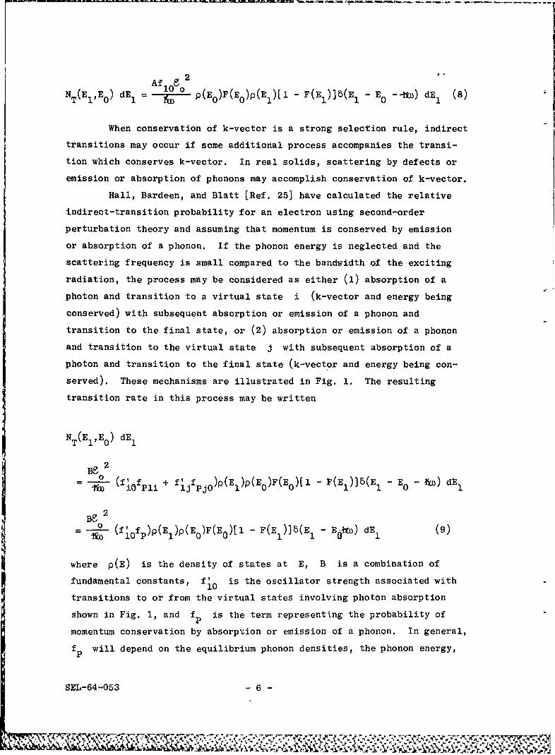
Hall, Bardeen, and Blatt [Ref. 25] have calculated the relative
indirect-transition probability for an electron using second-order
perturbation theory and assuming that momentum is conserved by emission
or absorption of a phonon. If the phonon energy is neglected and the
scattering frequency is small compared to the bandwidth of the exciting
radiation, the process may be considered as either (1) absorption of a
photon and transition to a virtual state i (k-vector and energy being
conserved) with subsequent absorption or emission of a phonon and
transition to the final state, or (2) absorption or emission of a phonon
and transition to the virtual state j with subsequent absorption of a
photon and transition to the final state (k-vector and energy being con-
served). These mechanisms are illustrated in Fig. 1. The resulting
transition rate in this process may be written
NT(E1,E0 ) dE1
- (f! f + f Wfj)P(E)p(E)F(Eo)[l -F(E1)]b(E 1 - Eo - )dE-rxb i0 Phi ljfPjO 1 00 111
BF 2
- (fjofp)p(EI)p(E0)F(E0)[l - F(EI)]5(E - E.ftu) dE (9)
where p(E) is the density of states at E, B is a combination of
fundamental constants, fO is the oscillator strength associated with
transitions to or from the virtual states involving photon absorption
shown in Fig. 1, and f is the term representing the probability of
momentum conservation by absorption or emission of a phonon. In general,
f will depend on the equilibrium phonon densities, the phonon energy,
SEL-64-053 - 6 -

E
S PHONON EMISSION
f! OR ABSORPTION fl|$ a f P jo .
k
FIG. 1. INDIRECT TRANSITIONS INVOLVINGPHONONS.
and the deformation potential in the solid being considered. As a
result, it may be temperature dependent.
3. Relation of Transition Probability to the Optical Constants
At photon energies where excitation of electronic interband
transitions is the predominant absorption process in a solid, the transi-
tion probabilities derived above can be related to the optical constants.
The power absorbed per unit volume by the excitation of transitions is
given by
00
Power = 4f NT(El,EO) dE1 (10)
0
where N T(EEo) is the transition rate per unit volume due to
radiation at frequency w. Remembering that the conductivity 0- is
defined classically in terms of the absorption of power O~o2/2 per
unit volume,
- 7 - SEL-64-053

- 2 NT(EI,Eo) dE1 (ii)
0 0
Since copper and silver are nonmagnetic, 1 90 and a and Ke
are related to the index of refraction n and the extinction coefficient
k by [Ref. 20]
n2 - k2 = K and 2nk (12)e 0
One can consider Maxwell's equations in terms of a real and an imaginary
dielectric constant, El and 62 respectively, where
E1 = K and E2 - G (13)
e 2 wE0
The absorption coefficient a is defined as 49k/A, and may be written,
using Eq. (12), as
n- 0 (14)nce 0
where c is the velocity of light in free space.
Much of the information obtained from photoemission measurements
involves the absorption coefficient. In order to relate these data
through Eqs. (14)and (11) to the transition probabilities and the densities
of states, 't is often necessary to know the indeN of refraction n
as a functibn of a). Although n may be determined from K andethrough Eq. (12), and theoretical expressions for K and o- are
eavailable, the wave functions and selection rules in a solid are not
generally known well enough to permit accurate calculation of n. For
both copper and silver, n has been measured for photon energies from
1 to 25 ev, and where it is required their data will be used in reduc-
tion of the experimental results [Ref. 19].
B. INELASTIC SCATTERING
Inelastic scattering of energetic electrons in a solid can have a
pronounced effect on experimental results obtained from photoemission
studies. In addition to the lifetime broadening effect described pre-
viously, strong scattering reduces the probability of electrons escaping
from the solid without scattering and increases the probability of
SEL-64-053 -8 -
*j~j~. ~, ~' ;J. *1i~''.i~

electrons escaping from the solid after having scattered one or more
times. As a result of this scattering process, information on the energy
of the electron, after optical excitation, is destroyed to some extent,
since it is sometimes difficult to determine which of the escaping
electrons have not been scattered before escaping. It will be shown
that one of the most important electron-scattering mechanisms in a metal
is electron-electron scattering. In order to interpret photoemission
data, as quantitative a knowledge as possible of the effect of this
scattering process is necessary.
Consider a gas of electrons imbedded in a background of uniform
positive charges whose density is equal to that of the electrons. The
Hamiltonian of the system is
-2
H -E i 1 (15)2m -r.'
Siigj J
where the first term is the sum of the electron kinetic energies and the
second term corresponds to their coulomb interaction. The coulomb.th .th
interaction between the i and j electrons may be expanded in a
Fourier series in a box of unit volume
e - = 2 "e " exp ik - ij)] (16)
r -r k 2
Placing Eq. (16) in Eq. (15) gives
2
Pi exp(ik • (r. - r )H + 2 (17)
i kk
By introducing collective coordinates q and conjugate momenta p
the Hamiltonian in Eq. (17) has been expressed by Bohn and Pines (Ref. 4]
in terms of a long-range organized collective oscillation, H osc;
short-range screened coulomb interaction, Hsr; and the interaction
between collective fields and individual electrons, HI *
- 9 - SEL-64-035
_2
-+H + H (18)2m osc sr
H osc (Pk-k + cup qkq_k ) (19)k-'k
c
2 exp[i r - (20)
sr eE a k 2
k>k
c
ik~kC
where k is the cutoff wave vector,-or screening parameter, beyond
which organized oscillation is not possible, w is the plasma frequency,
and 8k denotes a unit vector in the k direction. Bohm and Pines
showed that the HI term is almost always negligible compared to 1sr,
and Quinn (using a self-energy or quasi-particle approach) shwed that
the mean free path for plasmon creation in aluminum, for electrons with
energies less than twice the Fermi energy, is much larger than the mean
free path for electron-electron scattering [Ref. 6. Assuming the same
is true in copper and silver,' the dominant interaction term in Eq. (18)
is that associated with electron-electron scattering, H sr over the
range of electron energy considered (0 to 11.5 ev above Fermi energy) in
the photoemission work to be described.
The free-electron-gas model assumed above is not a good approxima-
tion to metals such as copper and silver because of the d-bands which are
located only a few electron volts below the Fermi level. However, from
the experimental results, it seems most reasonable that the Hamiltonian
of these metals can be separated into components similar to those of the
free electron gas, and that H will again be the dominant interactionterm.sr
If H is considered as a small perturbation, the probability
per second of an electron in state (E',k') being scattered to state
term,
SEL-64-035 - 10 -
. . . .. . .

(E,k) and exciting an electron in state (Eo,ko) to state (El,kl)
is (Ref. 12i
P : < k',k 0 I k,k, > 2 (E' - E - + E0 ) (22)
To find the total probability of an electron with energy E' being
scattered to some other energy, Eq. (22) must be summed over all possiblestates corresponding to ko, k, k, kl, E, E,, and E O . This summation
may be carried out if the squared matrix element in Eq. (22) is known.
However, many features of the scattering process can be determined with-
out knowing the matrix element. The summation can be changed to an
integral by including the appropriate densities of states and Fermi
functions in the standard way. Using this approach, the probability per
second of an electron with energy E' being scattered to an energy
between E and (E + dE) is
PS(E',E) dE =f~ IM 1p(E)p(E 0)p(E 0 + El - E)F(E 0)(1. - F(E 0 + El - E)I0
[1 - F(E)] dE 1 dE0 (23)
12where IM j is the squared matrix element in Eq. (22). Defining
g(E',E) 2 -IM Ip(Eo)p(Eo + El - E)F(Eo)[l - F(E 0 + E' - E)] dE00
(24)
Eq. (23) becomes
PS(E',E) dE = p(E)[l - F(E)]g(E',E) dE (25)
and the probability of an electron with energy ' being scattered to
any energy is
E'
Ps(E') p(E)[l - F(E))g(E',E) dE (26)
01-- 11 - SEL-64-053

Motizuki and Sparks [Ref. 5) have calculated Ps(EI) exactly for a free
electron gas, assuming the Fermi function at absolute zero and Hsr
given by the Yukawa potential [Ref. 26]. They obtained for tne scatter-
ing probability for electrons with energy near the Fermi energy
(El - EF)2Ps(E')c (27)
where EF is the Fermi energy. For comparison, Eq. (26) calculated
assuming M to be a constant and assuming constant density of states
is
Ps (E') - (E' - EF) 2 (28)
The close agreement between Eqs. (27) and (28) indicates that the strong
energy dependence of the scattering probability is due to a large extent
to the summation over the states available to take part in the scatter-
ing, rather than to the matrix element.
The reciprocal of the transition probability given by Eq. (26)
is defined as the lifetime for scattering, T. Assigning an average
group velocity v (E') to electrons with energy E', the mean free pathg
for electron-electron scattering is
v (E')I(E') = v 9 (E')T(E') = (29)
C. PROBABILITY OF ELECTRON ESCAPE
1. Effect of Inelastic Scattering
Consider an electron excited to some energy E and momentum p
at a distance x from the surface of a semi-infinite solid as shown in
Fig. 2. This electron may have been either directly excited to this state
by absorption of a photon, or scattered to it by some scattering process.
In order for the electron to escape from the solid without any locs of
energy, it must 1) reach the surface without suffering an inelastic
collision, and 2) have a momentum component perpendicular to the surface
SEL-64-053 - 12 -
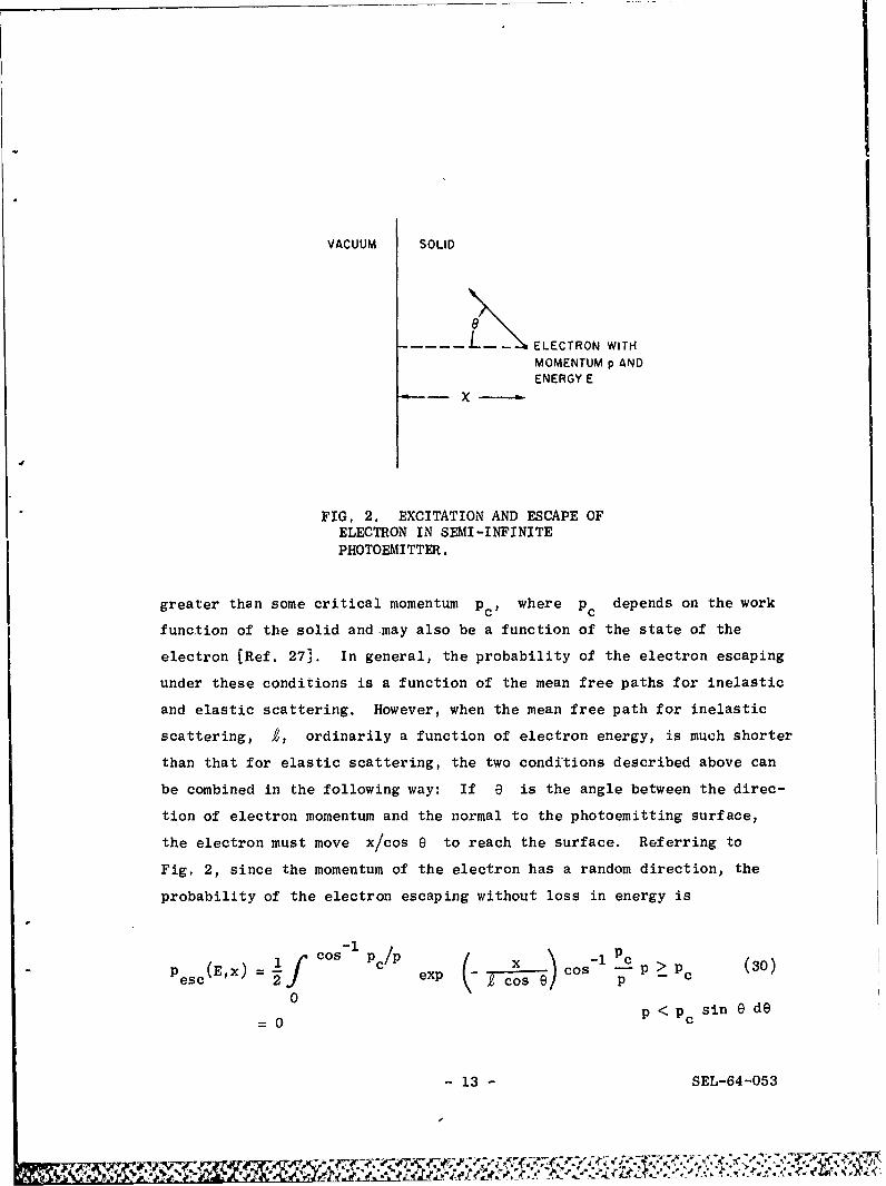
VACUUM SOLID
8 -ELECTRON WITH
MOMENTUM p AND
ENERGY E
FIG. 2. EXCITATION AND ESCAPE OFELECTRON IN SEMI-INFINITEPHOTOEMITTER.
greater than some critical momentum pc) where PC depends on the work
function of the solid and-may also be a function of the state of the
electron (Ref. 273. In general, the probability of the electron escaping
under these conditions is a function of the mean free paths for inelastic
and elastic scattering. However, when the mean free path for inelastic
scattering, 1, ordinarily a function of electron energy, is much shorter
than that for elastic scattering, the two conditions described above can
be combined in the following way: If 9 is the angle between the direc-
tion of electron momentum and the normal to the photoemitting surface,
the electron must move x/cos e to reach the surface. Referring to
Fig, 2, since the momentum of the electron has a random direction, the
probability of the electron escaping without loss in energy is
-I
If COlP PcPesc (E,x)= c exp Cos 9) cos - P > Pc (30)
=0P < P sin 0 dO
- 13 - SEL-64-053

Changing variables so that z = cos 0,
1
Pesc (E, x) = f exp - )dz P > PCpc/p
= 0 P < PC (31)
In optical absorption, the rate at which electrons are excited to
energies between E and (E + dE), in a slab of width dx located a
distance x from the photoemitting surface of a semi-infinite solid,
is of the form
G(Ex) dE dx = G (E)e dE dx (32)
where a is the absorption coefficient. From Eqs. (3) and (32), the
rate of escape of electrons with energy between E and (E + dE) is
00
R(E) dE = Go(E) dE f e-ax Pesc(E,x) dx (33)
0
Carrying out the integrations in Eq. (33) with respect to x and z
G 0(E) dE PC 1c 1+C 1
R(E) dE= -26 n - - -c ] (34)20 p OL 1 + (PC /p) 0:2,1
Defining as a threshold function C(E) = (i12)(1 - (pc/p)], Eq. (34)
can be simplified to
= KC(E)G (E) dE
a + (l/, )
where K, a correction factor, varies from 1/2 to 1 and is the function
of C(E) and a plotted in Fig. 3. The function C(E) is zero for
electron energies less than the work function above the Fermi level,
and has a maximum value of 0.5. The measurements on both silver and
SEL-64-053 - 14 -
S~c~a k'
~
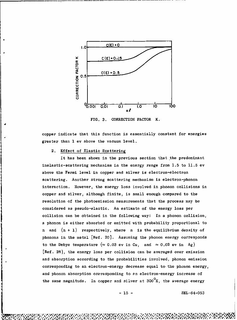
1.0o C(E) 0
C (E) zO.Ld5
C(E) 0.5z 0.50
Uw
0
o .. I I I
0.001 0.01 0.1 1.0 10 100=1
FIG. 3. CORRECTION FACTOR K.
copper indicate that this function is essentially constant for energies
greater than 1 ev above the vacuum level.
2. Effect of Elastic Scattering
It has been shown in the previous section that .the predominant
inelastic-scattering mechanism in the energy range from 1.5 to 11.5 ev
above the Fermi level in copper and silver is electron-electron
scattering. Another strong scattering mechanism is electron-phonon
interaction. However, the energy loss involved in phonon collisions in
copper and silver, although finite, is small enough compared to the
resolution of the photoemission measurements that the process may be
considered as pseudo-elastic. An estimate of the energy loss per
collision can be obtained in the following way: In a phonon collision,
a phonon is either absorbed or emitted with probability proportional to
n and (n + 1) respectively, where n is the equilibrium density of
phonons in the metal [Ref. 20). Assuming the phonon energy corresponds
to the Debye temperature (, 0.03 ev in Cu, and - 0.02 ev in Ag)
[Ref. 28), the energy loss per collision can be averaged over emission
and absorption according to the probabilities involved, phonon emission
corresponding to an electron-energy decrease equal tothe phonon energy,
and phonon absorption corresponding to sn electron-energy increase of
the same magnitude. In copper and silver at 300°K, the average energy
- 15 - SEL-64-053
-,?r W
I MUNLMOM .Nd~f XF ]L -" WSAI IJ - - -I~'
loss per collision is g 0.016 ev and - 0.0075 ev respectively. These
values justify the assumption that phonon collisions are lossless.
The process of electron escape from a photoeinitter when the mean
free path for elastic scattering is comparable to that for inelastic
scattering is difficult to describe exactly in closed mathematical form.
However, it has been found that the probability of escape of an electron
with energy E a distance x from the surface of a photoemitter can
be approximated in this case by
Pesc (E,x) = B(E)ex/L (36)
where B(E) is a function which takes into account the threshold, and
L is an attenuation length which depends on the mean free paths for
inelastic and elastic collisions [Ref. 29]. Using Eq. (36), calculations
similar to those resulting in Eq. (35) give
B(E)G0(E) dER(E) dE : (37)
a+ (l/L)
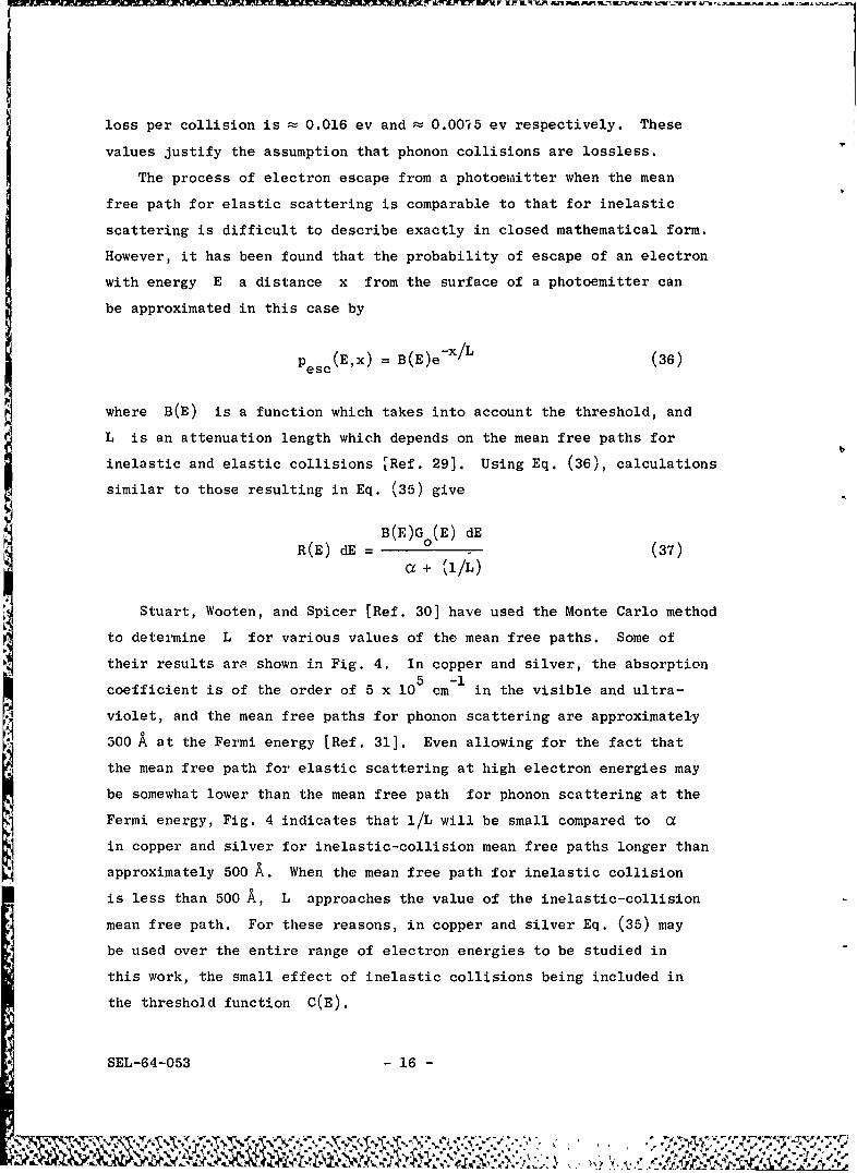
Stuart, Wooten, and Spicer [Ref. 30] have used the Monte Carlo method
to determine L for various values of the mean free paths. Some of
their results are shown in Fig. 4. In copper and silver, the absorption5-1coefficient is of the order of 5 x 105 cm in the visible and ultra-
violet, and the mean free paths for phonon scattering are approximately
300 A at the Fermi energy [Ref. 311. Even allowing for the fact that
the mean free path for elastic scattering at high electron energies may
be somewhat lower than the mean free path for phonon scattering at the
Fermi energy, Fig. 4 indicates that l/L will be small compared to a
in copper and silver for inelastic-collision mean free paths longer than
approximately 500 A. When the mean free path for inelastic collision
is less than 500 A, L approaches the value of the inelastic-collision
mean free path. For these reasons, in copper and silver Eq. (35) may
be used over the entire range of electron energies to be studied in
this work, the small effect of inelastic collisions being included in
the threshold function C(E).
SEL-64-053 - 16 -

I I i
1400-
40 4001
200
zo- o io 5o oozo
100 0 10 50 0020
FIG. 4. ATTENUATION LENGTH L CALCULATED USING MONTE CARLOMETHOD AS A FUNCTION OF ELECTRON-ELECTRON MEAN FREE PATHI6 AND ELECTRON-PHONON MEAN FREE PATH j .
D. ENERGY DISTRIBUTION OF THE PHOTOEMITTED ELECTRONS
Consider electrons in a solid with energy between E and (E + dE)
several electron volts above the Fermi level. Electrons may result in
this energy range due to either scattering from other energies or
photon excitation from states below the Fermi level. Defining
G opt (E,x) dE dx and G sc (E,x) dE dx as the rate of generation per
unit area due to optical excitation and to scattering respectively in
a slab of material of width dx a distance x from the photoemitting
surface, the contribution of each to the photoemission may be determined.
The absorption coefficient of a solid, a, at frequency CU may be
defined as
f(al)w= ] dE (38)E F
17 -SEL-64-053

where, a'(wE) dE is that part of a(w) due to electronic transitions
to energy states between E and (E + dE) (the Fermi function at O0K
has been assumed). If n is the flux of photons that is absorbed byPthe photoemitting material per unit area at frequency te, then
G (pt ,x) dE dx = np a'(,E) dE e<- x dx (39)
In both copper and silver, the effect of scattering is small enough
over the electron energy range studied that only those electrons which
escape without scattering and those which scatter once before escaping
need be considered. The probability of an electron scattering once
before escaping is derived exactly in Appendix A. However, the
following simple model of the process gives results which agree closely
to the detailed calculations, and illustrates the important features.
Suppose that the mean free path for scattering at energy E' is
small compared to the absorption depth so that a negligible fraction
of electrons excited optically to that energy escapes without scattering.
From Eqs. (25) and (26), a fraction [ps(E',E) dE]/Ps(E') of the
electrons optically excited to E' are scattered once to an energy
between E and (E + dE). If this scattering takes place in a distance
small compared to the absorption depth so that the spatial distribution
of the electrons after scattering is essentially the same as after
optical excitation, then the generation rate at E due to once-scattering
of electrons optically excited to El is
Ps(E,E') dE Gop(E',x) dx
Gsc(E,x) dE dx = opt (40)P (E')
The total generation rate at E due to scattering is given by (40)
integrated over all E.
E44a,EFfi Ps(EE')G ot(E' x) dE'
Gsc(E,x) dE dx = dx dE f so pt ) (41)E P (E')
E s
SEL-64-053 - 18 -
1M * ~~ -' A _V

Electrons with energy E' can produce electrons at energy E either
by themselves being scattered to E or by scattering electrons from
states below the Fermi level to E. The probability for these two events
can easily be shown to be equal, so the generation rate at E due to
scattering is twice that given by Eq. (41).
Combining Eqs. (39) and (41), and substituting in Eq. (35), the
number of electrons per absorbed photon that escape from a photoemitter
with energy between E and (E + dE) at frequency wn isEN(E) dE = KC(E)(,E) dE + 2 Ps (E',E) 7('(,E')(cc) + I (7E() ,
(42)
The energy distribution of photoemitted electrons may be related
to densities of states and transition probabilities by noting, from
Eqs. (11) and (14), that
CO
ncOPo 0
Comparing Eq. (43) to Eq. (38)
2tiNT (.,E )
a' E 26,E) = TE 1 E ) (44)
ncE0 0
An interesting special case occurs when L(E) is long compared to
1/[a(w)] and the fraction of electrons that escape after scattering is
negligible. This occurs in copper and silver for A1ro up to a few
electron volts larger than the work function. From Fig. 3, K is
unity for al >> 1, so Eq. (42) reduces to
N (E) dE C(E)ai(aO E) dE (45)
= a()(
- 19 - SEL-64-053

Using Eqs. (43) and (44)
N (E) dE = C(E)NT(E,Eo) dE (46)C() CE: (8
f NT(E',Eo) dEi0
If conservation of k-vector is not important for the optically excited
transitions, the expression for NT(E,E0 ) given in Eq. (8) can be used
in Eq. (46). Assuming the Fermi function at absolute zero, this
becomes
N (E) dE = C(E)f 1 0 p(E)p(E - r) dEEF+
f flOp,(E')p(E' - hiw) dE'EF
and if f is energy independent,
NW(E) dE = C(E)p(E)p(E - L) dE (48)
EF+kf p(E')p(E' - hw) dE'
EF
where EF is the Fermi energy. It is the expression for the energy
distribution given in Eq. (48) that is used to determine the density
of states in copper and silver over the energy range for which the
assumptions are valid.
The E used in Eq. (42) is the electron energy measured inside the
photoemitting material. This energy is related to the electron energy
in vacuum, Ev, which is determined from photoemission studies by
Ev = E - EF - EW (49)
where E is the work function of the photoemitting metal.
SEL-64-053 - 20 -

E. QUANTUM YIELD
The quantum yield is defined as the total number of electrons that
escape into vacuum from a photoemitting material per absorbed photon.
From this definition, and since C(E) in Eq. (42) is zero for E less
than (EF + EW), the quantum yield is
Y(rii) f N (E) dE (50)
E +EEFW
where N (E) dE is given by Eq. (42). From quantum-yield measurements,
the value of EW may be determined and a comparison between the
strengths of transitions to staLes above the vacuum level to those
between the vacuum level and the Fermi level may be made.
The yield pcr absorbed photon Y is related to the yield per
incident photon Y' through the reflectivity Re
Y = [1 - R(fW))Y( (u) (51)
- 21 - SEL-64-053
I V, I., -0,

HII. EXPERIMENTAL PROCEDURE
A. THE PHOTOTUBE
A picture of a phototube used in the photoemission studies is shown
in Fig. 5, and a diagram showing typical dimensions is shown in Fig. 6.
The stem presses, made of uranium glass, have eight 0.050-in. tungsten
pins, and the envelope of the tube is pyrex. Nonex glass was originally
used in the tubes, but it was found that in tubes using this glass it
was difficult to deposit and maintain a monolayer of cesium on the sur-
face of the photocathodes, apparently due to reaction between Cs and
envelope. This difficulty disappeared when uranium or pyrex glass was
used.
The collector can is formed from 0.005-in. sheet nichrome and
cleaned in trichlorethylene, acetone, distilled water, and alcohol.
After drying, it is fired in dry hydrogen for 10 min at 1000 C, then
mounted on a stem as shown in Fig. 7. There is a metal shield inside
the can to prevent copper or silver from depositing on the window of
the tube during evaporation. Two cesium channels, obtained from Radio
Corporation of America, Princeton, N.J., are shown in the figure.
These channels consist of approximately four parts of pure Si or Zr
powder and one part of Cs2CrO4 powder rolled in thin nickel sheet
and crimped. Cesium is given off when a channel is heated to
Pa
FIG. 5. PHOTOGRAPH OF EXPERIMENTAL PHOTOTUBE.
SEL-64-053 - 22 -
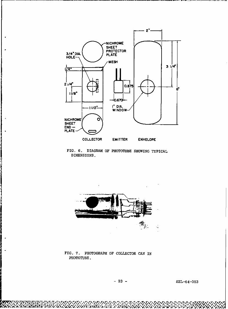
NICHROMESHEET
PCPROTECTOR3/4" DIA. PLATEHOLE
Q / -MESH 114'
21/4" 0 ..2'Li
F IG. 6.D A I DIA.WINDOW
NICHROMEN 0SHEETEND -PLATE7Q-
COLLECTOR EMITTER ENVELOPE
FIG. 6. DIAGRAM OF PHOTOTUBE SHOWING TYPICALDIMENSIONS.
FIG. 7. PHOTOGRAPH OF COLLECTOR CAN INPHOTOTUBE.
- 23 - SEL-64-053
?v
approximately 700 C. The plate between the cesium channels and the
collector can prevents impurities in the channels from getting
directly onto the photocathode.
The photocathode is cut from 0.050-in. grade A nickel, and polished
on progressively finer emery paper ending with 4/0. The plate is
polished to a mirror finish with diamond paste and mounted on a stem
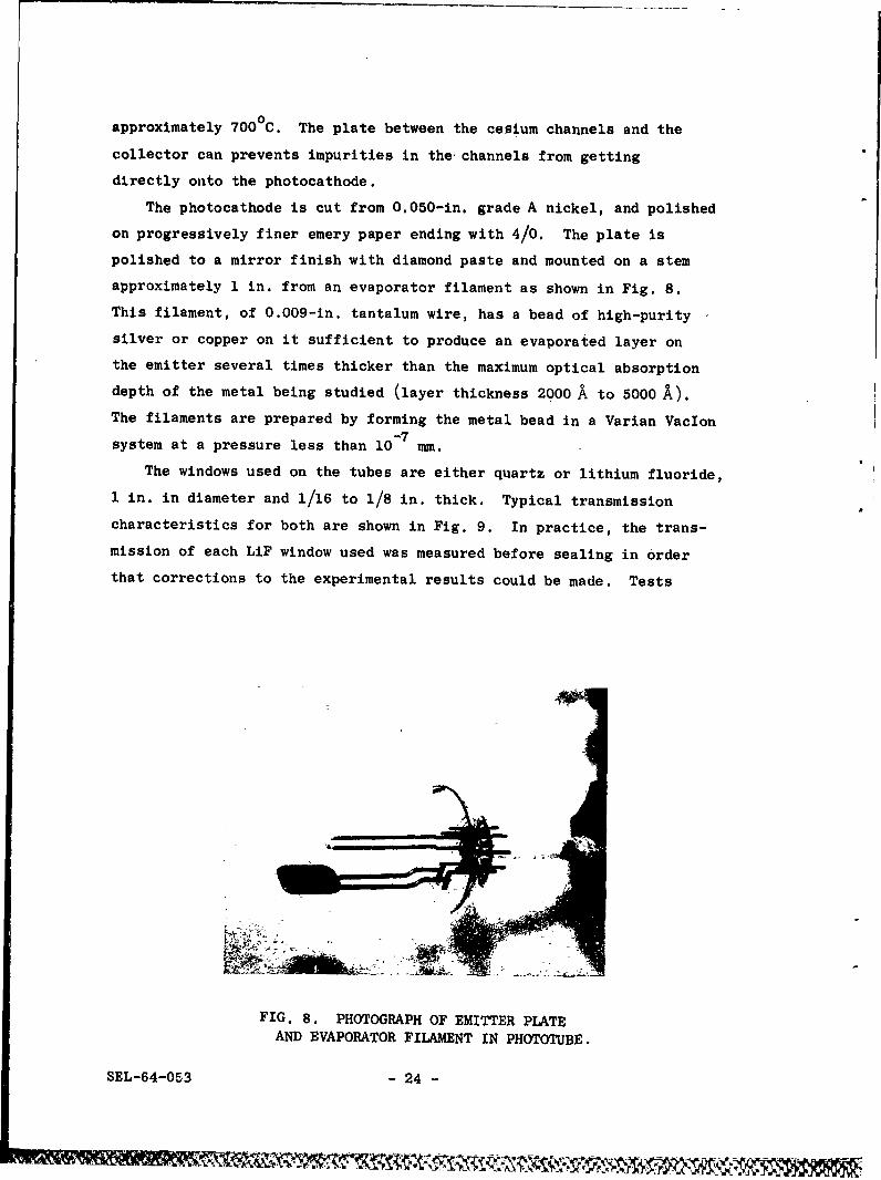
approximately 1 in. from an evaporator filament as shown in Fig. 8.
This filament, of 0.009-in. tantalum wire, has a bead of high-purity
silver or copper on it sufficient to produce an evaporated layer on
the emitter several times thicker than the maximum optical absorption
depth of the metal being studied (layer thickness 2000 A to 5000 A).The filaments are prepared by forming the metal bead in a Varian VacIon
-7system at a pressure less than 10 mm.
The windows used on the tubes are either quartz or lithium fluoride,
1 in. in diameter and 1/16 to 1/8 in. thick. Typical transmission
characteristics for both are shown in Fig. 9. In practice, the trans-
mission of each LiF window used was measured before sealing in order
that corrections to the experimental results could be made. Tests
FIG. 8. PHOTOGRAPH OF EMITTER PLATEAND EVAPORATOR FILAMENT IN PHOTOTUBE.
SEL-64-053 - 24 -

100
C
z 50
0 2 3 4 5 6 7 8 9 10 II 12
PHOTON ENERGY (eV)
FIG. 9. TYPICAL WINDOW TRANSMISSION CHARACTERISTICS.
indicated that no measurable change in window transmission characteristics
occurs in the sealing process. The quartz windows can be sealed directly
to the pyrex envelopes using AgCl but, due to the large expansion
coefficient of LiF, the LiF windows must be sealed first to a thin
(0.010-in.) high-purity silver ring which is then sealed to the
envelopes.
Prior to sealing, the windows are prepared by sandblasting a 1/8-in.
ring on the edge of one surface with fine alumina powder. The surfaces
to be sealed are painted with a thin coat of Hanovia 0.05 liquid bright
platinum paint which is fired on at 500 C. While hot, the painted areas
of the window and envelope are "tinned" with silver chloride, which
melts at approximately 500 C. The silver ring is prepared by annealing
in a hydrogen furnace for 10 min at 750°C.
To seal the quartz windows, the window is placed on the envelope in
the correct position, and the temperature raised until the silver
chloride just melts. Additional silver chloride is "painted" around
the seal, and the oven is allowed to-cool overnight. A similar pro-
cedure is followed for the LiF windows, except that the silver rings
are included in the sealing process.
The stem carrying the eiaitter plate is mounted in a vacuum bell jar
and covered by a molybdenum cylinder. The cylinder is heated with radio
frequency to approximately 850 C for 15 min to clean the plate, then
- 25 - SEL-64-053
~~%~p~~yjy -A-%~ -_M Z4

removed. The two stems and the envelope are sealed together under a
constant flush of 90/10m forming gas to retard oxidation of the metal
parts, and the tube sealed on a pump station for processing.
Processing of the tubes is done in the following manner. After
evacuation and baking at 2500C for several hours (pressure - 10-8mm),
the cesium channels are outgassed by slowly increasing the current
passed through them. When a current is reached where cesium is beginning
to be given off, as determined by the onset of measurable photoemission
from the photocathode, the current through the cesium channels is shut
off. The metal to be studied is then evaporated onto the photocathode.
After evaporation, the cesium channels are fired again, the photo-
current as a function of time being measured. Since the work function
of silver or copper is reduced to a minimum when approximately a uniform
monatomic layer of cesium is on the surface of the sample, the photo-
current should reach a peak, then begin to decrease as a function of
time. When the peak in photocurrent is reached, the cesium channels
are shut off and the tube is baked at 1000C. This baking process allows
the cesium to spread uniformly throughout the tube. In addition, the
last atomic layer of cesium on a surface is generally much more difficult
to remove than additional layers due to the strong attraction between
cesium and most other substances. For these reasons, essentially all
but the last layer of cesium atoms are pumped away during this baking
process. This is verified by measuring the photoemission as a function
of time during the bake. It is found that the emission current gradually
increases to approximately the same maximum value as measured during
the depositing of the cesium. The tube is then cooled to room tempera--8
ture and sealed off, generally at a pressure of about 10 mm or better.
The way in which the tubes are processed assu'es that a reasonably
uniform layer of cesium is deposited on the cathode and collector, and
that the work function of the collector is approximately the same as
that of the cathode. By using a microscope lamp focused to a small
area on the photocathode or collector, and by measuring the photocurrent,
this variation of the work function with position can be determined.
In all tubes used for these studies, the variation was small.
SEL-64-053 - 26 -
* ?'~L
B. ENERGY-DISTRIBUTION MEASUREMENTS
Suppose N (E) dE electrons are emitted per second in the energy
range between E and (E + dE) by a photoemitter due to radiation at
a frequency 0), the energy being measured in vacuum. The photocurrent
that flows when a voltage V is applied to a collecting electrode is
00
I W(V) = e J NC(E) dE (52)
-eV
where the voltage V includes the difference in contact potential
between the collector and cathode. In this expression, the effect of
space charge in the region between the collector and the photoemitter
has been neglected. (The errors involved in this assumption will be
described later.) The small-signal conductance of the tube at voltage
V is0
dI(V° ) 2gW(V dI ) dV) = e2 N(-eV) (53)
indicating that the energy distribution of photoemitted electrons can
be determined by simply measuring the phototube small-signal condactance
as a function of retarding potential.
Measurements of the energy distribution of photoemitted electrons
have been made by carefully measuring the I-V curve of a phototube
illuminated with light at the desired frequency, and graphically
differentiating the curve with respect to voltage [Ref. 32). This tech-
nique requires extremely accurate determination of the I-V curve, and
any small noises in the measurements generally lead to significant errors.
Spicer has used an ac method to perform the differentiation electroni-
cally, thus directing measuring the energy distribution of the photo-
emitted electrons and obtaining more accurate results with less sensitive
equipment (Ref. 33]. A new system based on the one described by Spicer,
but including some modifications and improvements, was used in this
work and will be described in detail.
- 27 - SEL-64-053
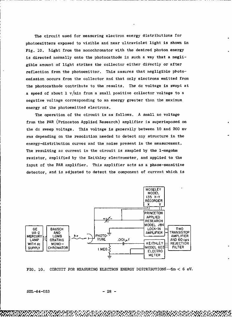
The circuit used for measuring electron energy distributions for
photoemitters exposed to visible and near ultraviolet light is shown in
Fig. 10. Light from the monochromator with the desired photon energy
is directed normally onto the photocathode in such a way that a negli-
gible amount of light strikes the collector either directly or after
reflection from the photoemitter. This assures that negligible pboto-
emission occurs from the collector and that only electrons emitted from
the photocathode contribute to the results. The dc voltage is swept at
a speed of about 1 v/min from a small positive collector voltage to a
negative voltage corresponding to an energy greater than the maximum
energy of the photoemitted electrons.
The operation of the circuit is as follows. A small ac voltage
from the PAR (Princeton Applied Research) amplifier is superimposed on
the dc sweep voltage. This voltage is generally between 10 and 200 mv
rms depending on the resolution needed to detect any structure in the
energy-distribution curves and the noise present in the measurement.
The resulting ac current in the circuit is sampled by the 1-megohm
resistor, amplified by the Keithley electrometer, and applied to the
input of the PAR amplifier. This amplifier acts as a phase-sensitive
detector, and is adjusted to detect the component of current which is
MOSELEYMODEL
135 X-YRECORDERx Y
PRINCETONE APPLIED- RESEARCH
MODEL JB41
GE BAUSCH LOCK-IN - TWOUA-2 AND AMPLIFIER TRANSISTORMERCURY LOMB hy ' PHOTO--/ 1MPLIIER
LAMP GRATING 1-TUBE .O01'af IAND60OcpsWITH dc MONO- H IKEITHLEY REJECTIONLAP GRTN TB MODEL AND FILTER
SUPPLY CHROMATOR I MEG MODEL 603 FILTER
-- -- METER
FIG. 10. CIRCUIT FOR MEASURING ELECTRON ENERGY DISTRIBUTIONS--fit < 6 eV.
SEL-64-053 - 28 -
proportional to the small.-signal conductance of the phototube. The
phase of the PAR amplifier is adjusted by turning off the light to the
phototube and settin, the phase control of the instrument for zero out-
put. Since the ac da-rk current of the tube is essentially all capaci-
tive, this adjustment assures that only the conductive component of
current is detected.
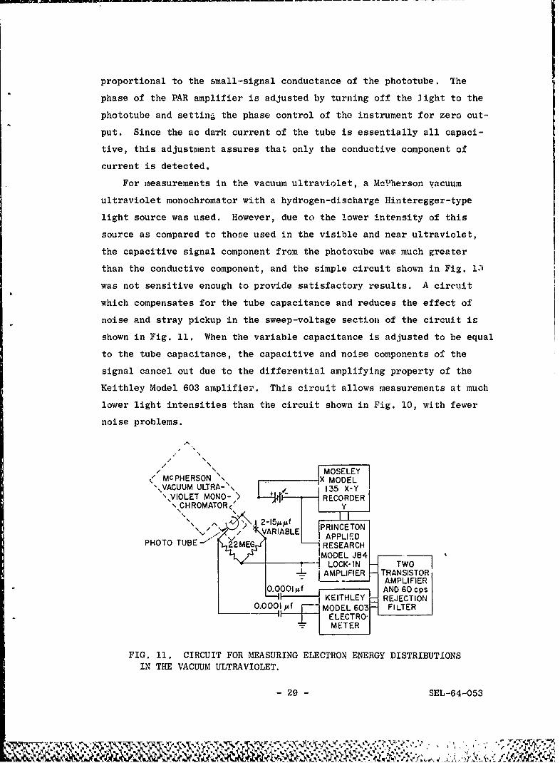
For measurements in the vacuum ultraviolet, a McPherson vacuum
ultraviolet monochromator with a hydrogen-discharge Hinteregger-type
light source was used. However, due to the lower intensity of this
source as compared to those used in the visible and near ultraviolet,
the capacitive signal component from the phototube was much greater
than the conductive component, and the simple circuit shown in Fig. 1
was not sensitive enough to provide satisfactory results. A circuit
which compensates for the tube capacitance and reduces the effect of
noise and stray pickup in the sweep-voltage section of the circuit is
shown in Fig. 11. When the variable capacitance is adjusted to be equal
to the tube capacitance, the capacitive and noise components of the
signal cancel out due to the differential amplifying property of the
Keithley Model 603 amplifier. This circuit allows measurements at much
lower light intensities than the circuit shown in Fig. 10, with fewer
noise problems.
/%
/ M MOSELEY<' MCPHERSON ", X MODEL
,VACUUM ULTRA-\ 135 X-Y',VIOLET MONO- > --- RECORDER\ CHROMATOR< Y
\ \/ ',2-15p j~f PRINCETON".,,E/" .,'" "VARIABLE APPLlrD
PHOTO 22MEG RESEARCH
MODEL JB4"t "LOCK- IN - TWO
_L jAMPLIFIER - TRANSISTOR- . - AMPLIFIER
O.O00f AND 60 cps- KEITHLEY REJECTION
0.0001 MODEL 603 FTERELECTRO-
- METER
FIG. 11. CIRCUIT FOR MEASURING ELECTRON ENERGY DISTRIBUTIONS
IN THE VACUUM ULTRAVIOLET.
- 29 -SEL-64-053
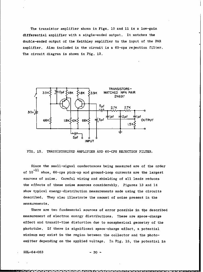
The transistor amplifier shown in Figs. 10 and 11 is a low-gain
differential amplifier with a single-ended output. It matches the
double-ended output of the Keithley amplifier to the input of the PAR
amplifier. Also included in the circuit is a 60-cps rejection filter.
The circuit diagram is shown in Fig. 12.
TRANSISTORS -3.9K 1 IO 8K 1.8K 3.9K MATCHED NPN PAIR
2N697
+ 2.7K 2.7K
1.5 K68K .8K OK 68K} 1501.5K UTU
INPUT
FIG. 12. TRANSISTORIZED AMPLIFIER AND 60-CPS REJECTION FILTER.
Since the small-signal conductances being measured are of the order-11
of 10 mhos, 60-cps pick-up and ground-loop currents are the largest
sources of noise. Careful wiring and shielding of all leads reduces
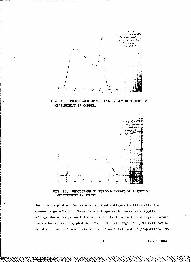
the effects of these noise sources considerably. Figures 13 and 14
show typical energy-distribution measurements made using the circuits
described. They also illustrate the amount of noise present in the
measurements.
There are two fundamental sources of error possible in the described
measurement of electron energy distributions. These are space-charge
effect and transit-time distortion due to nonspherical geometry of the
phototube. If there is significant space-charge effect, a potential
minimum may exist in the region between the collector and the photo-
emitter depending on the applied voltage. In Fig. 15, the potential in
SEL-64-053 - 30,
/ '
FIG. 13. PHOTOGRAPH OF TYPICAL ENERGY DISTRIBUTION
MEASUREMENT IN COPPER.
-- Z
FIG. 14. PHOTOGRAPH OF TYPICAL ENERGY DISTRIBUTIONMEASUREMENT IN SILVER.
the tube is plotted for several applied voltages to illustrate the
space-charge effect. There is a voltage region near zero applied
voltage where the potential minimum in the tube is in the region between
the collector and the photoemitter. In this range Eq. (52) will not be
valid and the tube small-signal conductance will not be proportional to
- 31 - SEL-64-053

vc POSITiVE
+w
J V NEAR ZERO
0 MINIMUM
V- N VOTENTIAL
EMITTER DISTANCE COLLECTOR
FIG. 15. ILLUSTRATION OF POTENTIAL IN PHOTOTUBEBETWEEN EMITTER AND COLLECTOR SHOWING POTENTIALMINIMUM DUE TO SPACE CHARGE.
the energy distribution of the photoemitted electrons. Reducing the
emission rate of electrons by decreasing the incident light intensity
will limit the voltage range over which distortion occurs, and at
sufficiently low light intensities the distortion will be negligible.
Figure 16 shows energy-distribution measurements made on a phototube at
various light intensities, and illustrates the distortion which can
result due to space-charge effects. In all the measurements reported
in this work, care has been taken to use light intensities low enough
to keep distortion due to space charge negligible.
The second fundamental source of error in the measurement of N (E)
is the transit-time effect. If the tube geometry is nonspherical,
there will be a spread in transit times for electrons emitted in different
directions or from different areas of the cathode. If the difference
in transit time is comparable to the period of the small ac voltage
used in the measurements, the small-signal conductance of the photctube
will not be proportional to N (E). An estimate of the distortion due
to this effect can be obtained by calculating the transit time of an
electron for the longest trajectory in the tube as a function of
emission energy, assuming that the electron just reaches the collector
with zero velocity. In the phototubes used, the maximum distance from
SEL-64-053 - 32 -
P,'* . '-

1,,1 I°<11 <12<Ia
z
z
0
w
ELECTRON ENERGY
FIG. 16. ENERGY DISTRIBUTION CURVES MEASURED
AT A SINGLE PHOTON ENERGY AT SEVERAL LIGHT
INTENSITIES I.
emitter to collector is of the order of 3 cm, giving for a calculated
transit time approximately
= 3 x 1O-4 se (54),/E-
where E is in electron volts. Since the ac measurements are made at
20 cps, this time must be comparable to 1/20 sec for this effect to
cause significant distortion. This only occurs for E within about
0.001 ev of zero, and for this reason the effect is neglected.
C. QUANTUM-YIELD MEASUREMENTS
The circuit for measuring relative quantum yield in the visible
and near ultraviolet region of the spectrum is shown in Fig. 17.
Chopped light at 20 cps is directed onto the phototube at the desired
photon energy, and the resulting 20 cps photocurrent that flows is
measured using the Keithley electrometer as a preamplifier and using
the lock-in amplifier as an amplitude detector. The collector of the
phototube during measurement is maintained at a sufficiently positive
voltage so that all electrons emitted from the cathode are collected
- 33 - SEL-64-053

PRINCETONPHOTODIODE APPLIED30v O W1f RESEARCH
f~I MODELLIGHT %B4 LOCK-INCHOPPER IMeg AMPLIFIER
20cpsL 1Zv O.O0I I
HIGH U GRATIG htL 603SOURCE AND I MONOCHRO - )N7 Meg ELECTRO-
IPOWER Y MATOR PHOTO METERCOR I G U-
COLOR FLTER
MEASUREMENT OF PHOTO TUBE RESPONSE
.... IPRINCETONPHOTDD~uIODE APPLIED
\30V_ O.O01,uf RESEARCHLIGHT + ~ll=- -("-' MODEL
CHOPPER I>Me ["-JB4 LOCK-IN2o0P[ g MeI AMPLIFIER
_ _I IIPEK XENON h BAUSCH iD BOLOMETERH4(IH PRESSURE GR hyw __
lSOURCEAN I MOW2%'OCHRPOWERSU / MATOR THERMOPILE
CORNINGCOLOR FILTER
MEASUREMENT OF RESPONSE OF STANDARD
FIG. 17. CIRCUIT FOR MEASURING RELATIVE QUANTUM YIELD--Ib < 6 ev.
and no electrons emitted from the collector reach the cathode (about
12 v). The photodiode in the circuit provides a signal for the PAR
amplifier that is at the same frequency as the chopping frequency.
The response of the phototube under study is compared to either a
Reeder Model RHL-7 thermopile or to a Barnes thermistor bolometer type
S 50-S. The response of both of these devices is proportional to the
incident power of the radiation over a wide range of light frequency.
Since at a given photon energy the photocurrent I from the photo-ph
tube is proportional to the rate of electron emission, and the response
of the thermopile or bolometer S is proportional to the number of
incident photons per second multiplied by the photon energy, the quantum
yield in electrons per incident photon of the phototube is
Y =K I S (55)1 S
SEL-64-053 -34
zY~ M , <(- - ' .-- ,- -e
where K is a constant. Using Eq. (55), the relative yield at
different photon energies can be determined by measuring S and Iph
at various incident light frequencies.
The constant K in Eq. (55) is determined at a single photon energy
by comparing the phototube under study to an RCA 934 phototube which
had been calibrated for absolute yield at a photon energy of 3.0 ev
by W. E. Spicer, and checked by H. R. Phillip at General Electric
Research Laboratories (Ref. 34).
When the photon energy is only slightly greater than the work
function of the photoemitter, the yield is many orders of magnitude
smaller than at much higher photon energies. For this reason, care must
be taken when making measurements near the photoemission threshold that
no scattered light of higher photon energy gets into the phototube.
Scattered light can be eliminated by placing Corning-glass color filters
between the light source and the monochromator, as shown in Fig. 17.
These filters are chosen to pass only the light with photon energy equal
to or less than the photon energy of the measurement.
Under incident radiation with photon energies greater than 4 ev,
it has been found that sodium salicylate fluoresces near 4200 A, giving
very nearly one photon at that wavelength per incident photon for inci-
dent photon energy greater than 4 ev. A phototube or photomultiplier
coated with sodium salicylate will have a response nearly proportional
to the number of incident photons per second for light with photon energy
greater than 4 ev. This property has been used to measure the quantum
yield of phototubes at photon energies greater than 4 ev, and is de-
scribed in detail by Kindig (Ref. 35]. The relative quantum yield
determined in this way is matched to the known absolute quantum yield
measured using the bolometer or thermopile.
- 35 - SEL-64-053
-%" 4'

IV. PHOTOEMISSION FROM COPPER
A. THE CALCULATED BAND STRUCTURE OF COPPER
Calculations of the energy-band structure of copper have recently
been made by Segall and Burdick [Refs. 2, 31. It is of importance to
describe the crystal potentials that were used in these calculations,
since the extremely close agreement between the calculated band structure
and the experimental results reported here indicates that the potential
was very accurately approximated.
In Segall's work, the band structure was calculated twice by the
Green's function method iRef. 36) using two different potentials. One
of the potentials used was that constructed by Chodorow [Ref. 37], andis the one which yields the 3d electron Hartree-Fock functions for the
free Cu+ ion. To this Segall added the contribution of a "metallic"
s electron function (the s function- for an electron of average energy).
The use of this potential implies the WVigner-Seitz approximation that
all conduction electrons, except those for the ui*!' cell under considera-
tion, are excluded from the cell by correlation and exchange interactions.
The potential might be expected to be most accurate for the d electrons.
Also, it includes the approximation that the same potential applies to
all angular momentum components of the wave function.
The core and d-electron Hartree-Fock functions for neutral copper
were renormalized in the Wigner-Seitz sphere and used for the second
potential. The coulomb and exchange contributions to the potential for
the various values of 2 were computed for a configuration which
included, in addition to the core and d electrons, a renormalized 's
function.
Segall fotind that the band structures calculated for the two different
potentials were very similar. The positions of the bands were somewhat
different, but the general features were the same.
Burdick calculated the band structure by the APW method [Ref. 38]
using the Chodorow potential described above. His results agreed with
those of Segall for the same potential to within 0.15 ev.
The band structure along the various symmetry axes in the reduced
zone calculated by Segall using the 2-dependent potential is shown in
SEL-64-053 - 36 -

Fig. 18. This band structure will be used in discussing the photo-
emission data. (Detailed comparisons of the data to the calculations
of both Segall and Burdick will be given in the text.) In Fig. 18
the points of symmetry are labeled according to the notation of Bouckaert,
Smoluchowski, and Wigner (Ref. 39). The relatively flat bands located
approximately 2 to 6 ev below the Fermi level are the d-bands. Because
of the flatness of the bands, they are characterized by a relatively
high density of states. The difference in energy between the vacuum
level marked on the figure and the Fermi level is the work function of
copper with approximately a monolayer of cesium on the surface. This
energy is determined by studying the quantum yield of a suitably treated
copper photoemitter as a function of photon energy.
(0.0.0 , (..0) (,.O ;1 f , 59.o.o c(j30 _(.00
02 W,
X4 ' 0. , L
a ,,
FIG. 18. CALCULATED BAND STRUCTURE
OF COPPER.
B. THE QUANTUM YIELD
Figure 19 shows the quantum yield of a copper photoemitter with
cesium on the surface. The solid curve is the measured yield per inci-
dent photon, corrected for the transmission of the LiF window of the
phototube. The dashed curve is the yield per absorbed photon determined
from the measured yield and the reflectivity of copper [Ref. 19).
In a theoretical treatment of photoemission from metals, Fowler
(Ref. 40) has derived the following equation for the quantum yield near
the threshold of photoemission:
37 SEL-64-053
.33 ~ ' A 3 3

I0"
- ELECTRONS /INCIDENT PHOTON
S..---- ELECTRONS/ABSORBED PHOTON
wIo"
! t.| 10!
W0I
0 1 2 3 4 5 6 7 8 9 0 If 12PH( )N ENERGY (eV)
FIG. 19. QUANTUM YIELD OF COPPER.
Y (4UEw) -> E
0 tiW < EW (56)
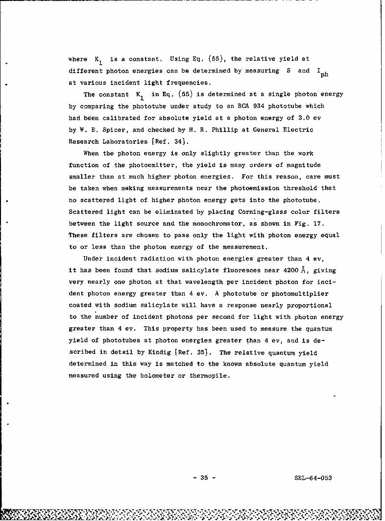
where Ew is the work function of the metal. From Eq. (56) a plot of
the square root of the yield as a function of photon energy should give
a straight line extrapolating to the work function for zero yield. Such
a plot for copper is shown in Fig. 20. The work function for copper
determined from Fig. 20 is 1.55 ev.
The general features of the quantum-yield curve shown in Fig. 19
are due to the d-bands. This can most easily be demonstrated by thefollowing argument. If scattering effects are negligible, the quantumyield can be written approximately as [Ref. 291
ay cc a (57)
a+aa b
where a is that part of the absorption coefficient due to transitionsa
to states above the vacuum level, and a b is that part due to transitions
to states between the Fermi level and the vacuum level. The decrease in
yield in Fig. 19 at about 2.1 ev photon energy is due principally to an
increase in ab, since at this energy electrons from the d-bands are
starting to be excited to states just above the Fermi level. At 3.7 ev
photon energy, d-band electrons can be excited to states above the vacuum
SEL-64-053 - 38 -
zrIn
- ,
z0DQ
Co
I-
-J
EW 1.55 eV
zE = II
0 1.4 1.5 1.6 1.7 1.8 1.9 2.0PHOTON ENERGY (eV)
FIG. 20. EVALUATION OF WORK FUNCTION OF COPPER WITH
CESIUM ON THE SURFACE.
level resulting in an increase in a a and in the yield. The slow
increase in yield at photon energies greater than 6 ev is due to
scattering, and will be explained in detail in Sec. G,
C. ENERGY DISTRIBUTION OF PHOTOEMITTED ELECTRONS--!4o 3.7 ev
At photon energies less than 3.7 ev, electrons excited from the
d-bands do not gain enough energy to be able to escape, and structure
in the energy distribution of photoemitted electrons is due almost
entirely to transitions from the p-like states just below the Fermi
level to s-like states just above the vacuum level. Details of the
band structure in these energy regions can be determined by studying
the energy distribution of photoemitted electrons.
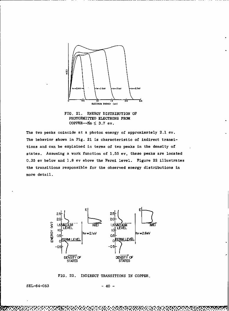
Figure 21 shows the energy distributions which result for photon
energies from 2.1 ev to 3.7 ev. Two peaks appear in the distribution,
one fixed in energy independent of Iic at about 0.25 ev above the
vacuum level, and the other with energy E given by
E = 1c - 1.90 ev (58)
- 39 - SEL-64-053
. .~, *
hy-2,16V hy.2 SeV In'.3 IOV h&'-3.7eV
05 io 15 20 2.5
ELECTRON ENERGY WcV)
FIG. 21. ENERGY DISTRIBUTION OFPHOTOEMITTED ELECTRONS FROMCOPPER--1f i 3.7 ev.
The two peaks coincide at a photon energy of approximately 2.1 ev.
The behavior shown in Fig. 21 is characteristic of indirect transi-
tions and can be explained in terms of two peaks in the density of
states. Assuming a work function of 1.55 ev, these peaks are located
0.35 ev below and 1.8 ev above the Fermi level. Figure 22 illustrates
the transitions responsible for the observed energy distributions in
more detail.
2.51 2.52.0 2.0
>.1.5 CUUM N(ELEVEL LEVEL
> 0- 1.0S0hv=2.IeV hy=2.8eV0.5- Q5_
LEVE RMILEVEL
-0.5 -05
DENSITY OF DENSITY OFSTATES STATES
FIG. 22. INDIRECT TRANSITIONS IN COPPER.
SEL-64-053 - 40 -

Comparing this experimentally determined density of states to the
calculated band structure in Fig. 18, it is evident that the peak 0.35
ev below the Fermi level is associated with symmetry point L' and that2
the peak 1.8 ev above the Fermi level is associated with symmetry point
4, since high densities of states result at symmetry points in the
band structure. Segall (Ref. 2] and Burdick (Ref. 33 indicate critical
points at X (2.3 or 2.0 ev, respectively, above the Fermi surface)
and at L' (0.8 or 0.6 ev, respectively, below the Fermi surface). The
energies at the symmetry points attributed to Segall are those calculated
assuming the 2-dependent potential.
D. TRANSITIONS FROM THE d-BANDS
At photon energies greater than 3.7 ev, electrons can be optically
excited from the d-bands to states above the vacuum level. These
electrons will appear in the energy distribution of the photoemitted
electrons at these photon energies. Figure 23 shows the energy distri-
butions for photon energies of 3.7 and 3.9 ev. At 3.7 ev there is very
little evidence of d-band electrons being excited to states above the
vacuum level. At 3.9 ev, however, a large number of slow electrons
0 05 10 15 20 2.5
ELECTRON ENERGY (eV)
FIG. 23. ENERGY DISTRIBUTION OF PHOTOEMITTED
ELECTRONS FROM COPPER--Ila) = 3.7 ev, 3.9 ev
- 41 - SEL-64-053
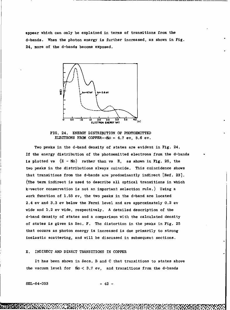
appear which can only be explained in terms of transitions from the
d-bands. When the photon energy is further increased, as shown in Fig.
24, more of the d-bands become exposed.
• hV, TeV hv,5.G*V
0 I .0 . 2.0 2.5 3.0 3. 4
ELECTRON ENERGY (I) 4(a)
FIG. 24. ENERGY DISTRIBUTION OF PHOTOEMITTED
ELECTRONS FROM COPPER--Kw= 4.7 ev, 5.6 ev.
Two peaks in the d-band density of states are evident in Fig. 24.
If the energy distribution of the photoemitted electrons from the d-bands
is plotted vs (E - YO) rather than vs E, as shown in Fig. 25, the
two peaks in the distributions always coincide. This coincidence shows
that transitions from the d-bands are predominantly indirect [Ref. 23].
(The term indirect is used to describe all optical transitions in which
k-vector conservation is not an important selection rule.) Using a
work function of 1.55 ev, the two peaks in the d-band are located
2.4 ev and 3,3 ev below the Fermi level and are approximately 0.2 ev
wide and 1.2 ev wide, respectively. A detailed description of the
d-band density of states and a comparison with the calculated density
of states is given in See. F. The distortion in the peaks in Fig. 25
that occurs as photon energy is increased is due primarily to strong
inelastic scattering, and will be discussed in subsequent sections.
E. INDIRECT AND DIRECT TRANSITIONS IN COPPER
It has been shown in Sees. B and C that transitions to states above
the vacuum level for &0< 3.7 ev, and transitions from the d-bands
SEL-64-053 - 42
0;F 0 . 0 1. 2. 2.v. . .

hz'=iO.4 eV
hv=8.6eV
hv,=6.2e
Z
hv=59eV
hv 5.5eV hp=5OeVhv=4.4eV
-6.0 -5.5 -5.0 -4.5 -4.0 -3.5E-hv (eV)
FIG. 25. ENERGY DISTRIBUTION OF PHOTOEMITTED
ELECTRONS FROM COPPER PLOTTED VERSUS E-Mo.
to states above the vacuum level can be adequately explained in terms
of indirect transitions. There is no evidence of direct transitions
in these cases. However, for photon energies above 4.1 ev, direct
transitions contribute to the observed results.
Referring to Figs. 21 and 24, the peak near the maximum electron
energy attributed to transitions from states near 12 in the calculated
band structure grows in size at -KM = 4.7 ev, and splits into two peaks
as shown for 1u = 5.6 ev. This behavior can be interpreted in terms
of indirect and direct transitions, and is illustrated using the calcu-
lated band structure in Fig. 26. When the photon energy Kw& is just
equal to the energy difference between L and L't a strong peak in1 2'
the energy distribution should occur near the maximum electron energy
due to the sum of both indirect and direct transitions from L'. At a
higher photon energy, KIf 2 , two peaks in the energy distribution should
appear, one due to direct transitions from states near L to states
- 43 - SEL-64-053
TirW~~
r ,e , . " . ,, --., .. . . .. .. ..

A
--. . - -- VAUUM LEVEL
"--FERMI LEVEL
X W L
FIG. 26. PORTION OF BAND STRUCTURE OF COPPER SHOWINGDIRECT AND INDIRECT TRANSITIONS.
near L (labeled A in Fig. 26), and one due to indirect transitions
from the high density of states near L' (labeled B). The peak due
to direct transitions will not have an energy given by Eq. (58-) since
the energy of the initial states will depend on 11W (see Fig. 26). In
general, it Will be found that the energy of the peak due to direct
transitions will increase in energy with lico more slowly than that
given by Eq. (58), but the peak due to indirect transitions will follow
Eq:. (58).
Figure 27 shows the portion of the energy distributions near the
maximum electron energy for several values of hw. The estimated frac-
tion of electrons due to direct transitions is shown by the cross-
hatched area. From this figure, it is apparent that the probability of
electrons being involved in indirect transitions is somewhat stronger
than that for direct transitions in the copper samples studied, a result
which is the complete opposite of the behavior in the semiconductors
Si and Ge [Ref. 14). No other evidence of direct transitions in
copper was found over the range of electron energy studied. In Fig. 28
the energy at the symmetry point L1 is determined. The vertically
plotted energy in the figure is the energy of the initial states
SEL-64-053 - 44 -
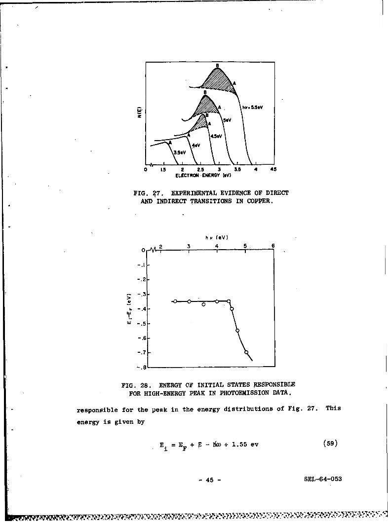
Ya
A
A 4 5 V4V
3.50V
0 1.5 2 2.5 3 3.5 4 43ELECTRON-ENERGY (eV)
FIG. 27. EXPERIMENTAL EVIDENCE OF DIRECT
AND INDIRECT TRANSITIONS IN COPPER.
hv (V)2 3 4 , . 6
I I I
-.1
S-.4
o.3 0 0
w -.5
FIG. 28. ENERGY OF INITIAL STATES RESPONSIBLE
FOR HIGH-ENERGY PEAK IN PHOTOEMISSION DATA.
responsible for the peak in the energy distributions of Fig. 27. This
energy is given by
E = F + E -liw + 1.55 ev (59)
- 45 - SEL-64-053
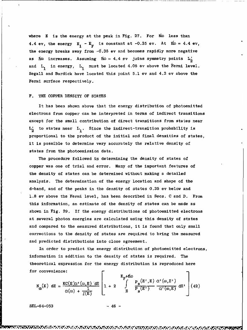
where E is the energy at the peak in Fig. 27, For Kto less than
4.4 ev, the energy Ei - EF is constant at -0.35 ev. At 16) = 4.4 ev,
the energy breaks away from -0.35 ev and becomes rapidly more negative
as fim increases. Assuming 11W = 4,.4 ev joins symmetry points L
and L 1 in energy, L 1 must be located 4.05 ev above the Fermi level.
Segall and Burdick have located this point 5.1 ev and 4.2 ev above the
Fermi surface respectively.
F. THE COPPER DENSITY OF STATES
It has been shown above that the energy distribution of photoemitted
electrons from copper can be interpreted in terms of indirect transitions
except for the small contribution of direct transitions from states near
LL to states near L . Since the indirect-transition probability is
proportional to the product of the initial and final densities of states,
it is possible to determine very accurately the relative density of
states from the photoemission data.
The procedure followed in determining the density of states of
copper was one of trial and error. Many of the important features of
the density of states can be determined without making a detailed
analysis. The determination of the energy location and shape of the
d-band, and of the peaks in the density of states 0.35 ev below and
1.8 ev above the Fermi level, has been described in Secs. C and D. From
this information, an estimate of the density of states can be made as
shown in Fig. 29. If the energy distributions of photoemitted electrons
at several photon energies are calculated using this density of states
and compared to the measured distributions, it is found that only small
corrections to the density of states are required to bring the measured
and predicted distributions into close agreement.
In order to predict the energy distribution of photoemitted electrons,
information in addition to the density of states is required. The
theoretical expression for the energy distribution is reproduced here
for convenience:
I E++2
NS(E) dE = -4-0(53E) +2 f p (E') a'(oE) cE' (42)1E Ps J a (oE
SEL-64-053 - 46 -

0
zW
FERMI VACUUMLL I LEVEL
I I I ! I I I I
-8 -6 -4 -2 0 2 4 6 a 10
ENERGY-FERMI ENERGY (eV)
FIG. 29. ESTIMATED DENSITY OF STATES OF COPPER.
The threshold function C(E) in copper is difficult to determine because
of the peak in the density of states just above the vacuum level. How-
ever, C(E) for silver is relatively easy to determine, and will be
used here (see Fig. 63 in Chapter V). Since silver and copper are very
similar metals, this assumption should result in only a small error,
The absorption coefficient a(bi) for copper is given in the literature
[Ref. 19]. The scattering parameters ps(E',E), Ps(E'), and L(E)
can be estimated using the density of states. (A detailed description
of these calculations is given in Sec. G.) The function c'(w,E) is
given in Eq. (44), and for indirect transitions is proportional to the
product of the initial and final densities of states if the squared
momentum matrix element is assumed constant.
Figures 30 and 31 show the measured and predicted energy-distribution
curves at two photon energies to illustrate the degree of accuracy
obtained after corrections to the density of states had been made. These
curves are indicative of the agreement obtained over the photon energy
- 47 - SEL-64-053
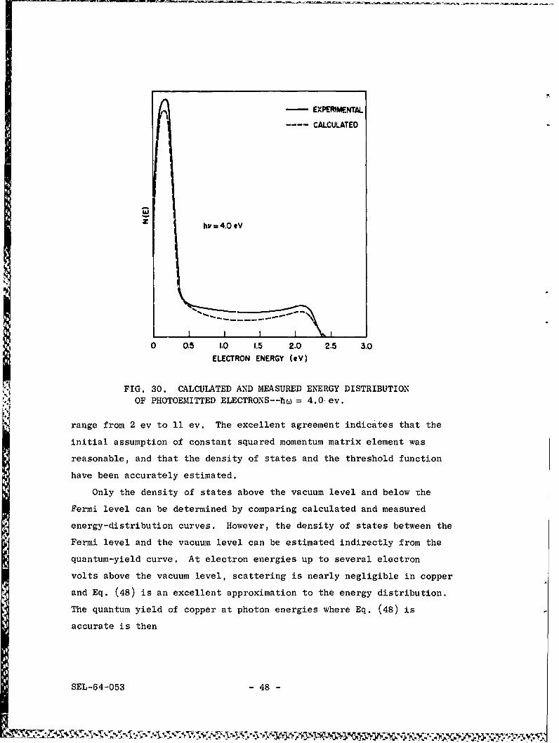
EXPERIMENTAL
---- CALCULATED
Z hy 4.0 eV
0 0.5 1.0 1.5 2.0 2.5 3.0
ELECTRON ENERGY (V)
FIG. 30. CALCULATED AND MEASURED ENERGY DISTRIBUTIONOF PHOTOEMITTED ELECTRONS--hw = 4.0- ev.
range from 2 ev to 11 ev. The excellent agreement indicates that the
initial assumption of constant squared momentum matrix element was
reasonable, and that the density of states and the threshold function
have been accurately estimated.
Only the density of states above the vacuum level and below the
Fermi level can be determined by comparing calculated and measured
energy-distribution curves. However, the density of states between the
Fermi level and the vacuum level can be estimated indirectly from the
quantum-yield curve. At electron energies up to several electron
volts above the vacuum level, scattering is nearly negligible in copper
and Eq. (48) is an excellent approximation to the energy distribution.
The quantum yield of copper at photon energies where Eq. (48) is
accurate is then
SEL-64-053 - 48 -
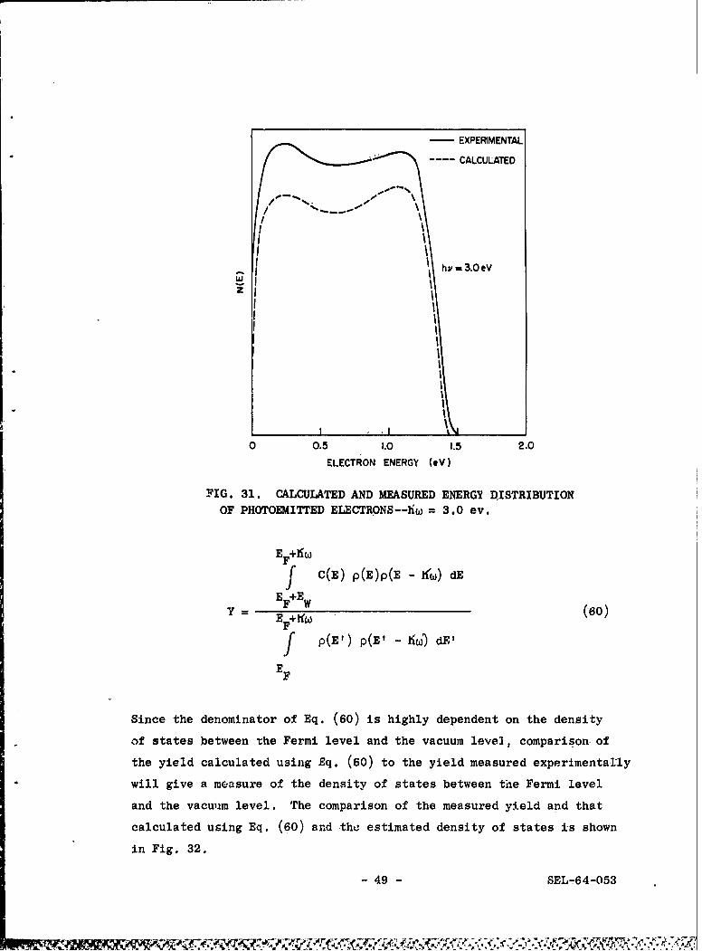
-EXPERIMENTAL
CALCULATED
hv ,3.0 eVZz
0 0.5 1.0 1.5 2.0ELECTRON ENERGY We)
FIG. 31. CALCULATED AND MEASURED ENERGY DISTRIBUTIONOF PHOTOEMITTED ELECTRONS--liw = 3.0 ev.
EF+E1W
Y= E.., W (60)
E F
Since the denominator of Eq. (60) is highly dependent on the density
of states between the Fermi level and the vacuum level, comparison-of
the yield calculated using Eq. (60) to the yield measured experimentally
will give a measure of -the density of states between the Fermi level
and the vacuum level. The comparison of the measured yield and that
calculated using Eq. (60) and the estimated density of states is shown
in Fig. 32.
ET 49 N SEL-64-053
FIG.31.CALCLATD A1D MASURD EERGYDITRIBTI7

% It
JO I O
CALCULATED
QJ CORRECTED FOR_ REFLECTION
W
.J
I-
0 1 2 3 4 5PHOTON ENERGY (e V Y)
FIG. 32. MEASURED AND CALCULATED QUANTUMYIELD FOR COPPER.
The dnsity of states derived from the trial and error methods
described is shown in Fig. 33 and compared to the density of sta'es
calcuated for copper by Burdick. The estimated accuracy in the
experimentally determined density of states is 15 percent. A more
detailed comparison of the d-band density of states determined here
with that cacuated by Burdick is given in Fig. 34.
G. THE EFFECT OF ELECTRON-ELECTRON SCATTERING
1. Lifetime Broadening
Electron-eectron scattering affects the photoemission data in
two ways. From Eq. (1), it is evident that if the scattering frequency
A of the states involved in optically excited transitions is arge
compared to the resoution of the measurements, a lifetime broadening
will occu. From Eq. (42), it can be seen that a short eectron-eectron
mean free path compared to 1/a will result in distortion of the
energy-distribution curves and will also result in an increased number of
electrons which escape after scattering one or more times.
SEL-64-053 50

EXPERIMENTAL-- BURDICK
WI,
F-l
It:t
L/ I
-8 -6 -4 -2 0 2 4 6 8 10 12 14 16 18ENERGY- FERMI ENERGY (eV)
FIG. 33. DENSITY OF STATES OF COPPER.
EXPERIMENT
F. 34.DESIT UOLATES O
Figures 25 and 35 illustrate the way in which the narrow peak near
the top of the d-band is broadened due to lifetime broadening as the
electrons are excited to higher energies. It is estimated that at
approximately 6 ev above the Fermi surface the peak is broadened to a
width of 0.3 ev from a width at low energies of 0.2 ev. Assuming at
this energy that A in Eq. (1) corresponds to an energy of 0.1 ev
lA= 0.1 ev (61)
- 51 - SEL-64-053
C=_-,
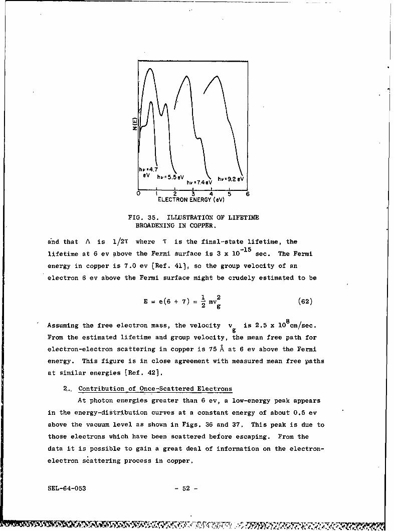
z
h =4.7eV hL=5.5eV hv=9.2 eV
- -I I t0 I 2 3 4 5 6
ELECTRON ENERGY (eV)
FIG. 35. ILLUSTRATION OF LIFETIME
BROADENING IN COPPER.
and that A is 1/2T where T is the final-state lifetime, the
lifetime at 6 ev above the Fermi surface is 3 x 10- 1 5 sec. The Fermi
energy in copper is 7.0 ev (Ref. 41), so the group velocity of an
electron 6 ev above the Fermi surface might be crudely estimated to be
1 2E = e(6 + 7) = - my (62)
Assuming the free electron mass, the velocity v is 2.5 x 10 8cm/sec.gFrom the estimated lifetime and group velocity, the mean free path for
electron-electron scattering in copper is 75 A at 6 ev above the Fermi
energy. This figure is in close agreement with measured mean free paths
at similar energies (Ref. 421.
2.. Contribution of Once-Scattered Electrons
At photon energies greater than 6 ev, a low-energy peak appears
in the energy-distribution curves at a constant energy of about 0.5 ev
above the vacuum level as shown in Figs. 36 and 37. This peak is due to
those electrons which have been scattered before escaping. From the
data it is possible to gain a great deal of information on the electron-
electron scattering process in copper.
SEL-64-053 - 52 -

10 2.0 30 40 50 60ELECTRON ENERGY (eV)
FIG. 36. ENERGY DISTRIBUTION OF PHOTOEMITTEDELECTRONS FROM COPPER--Kw = 7.1 ev.
he- 8.9 eV
O 2.0 30 40 50 60 7,0ELECTRON ENERGY (#V)
FIG. 37. ENERGY DISTRIBUTION OF PHOTOEMITTEDELECTRONS FROM COPPER--IW = 8.9 ev.
A theoretical expression for the energy distribution of photo-
emitted electrons including scattering is given approximately by
Eq. (42) and more exactly in Appendix A. In order to use these
expressions and the density of states to predict the energy distributions,
it is necessary to know the matrix element M for the scattering
probability in Eq. (23). Since the selection rules and wave functions
involved in the scattering process are not well known, and since the
Born approximation used in deriving Eq. (23) may not be valid in metals
such as copper and silver [Ref. 51, it is not in general possible to
- 53 - SEL-64-053
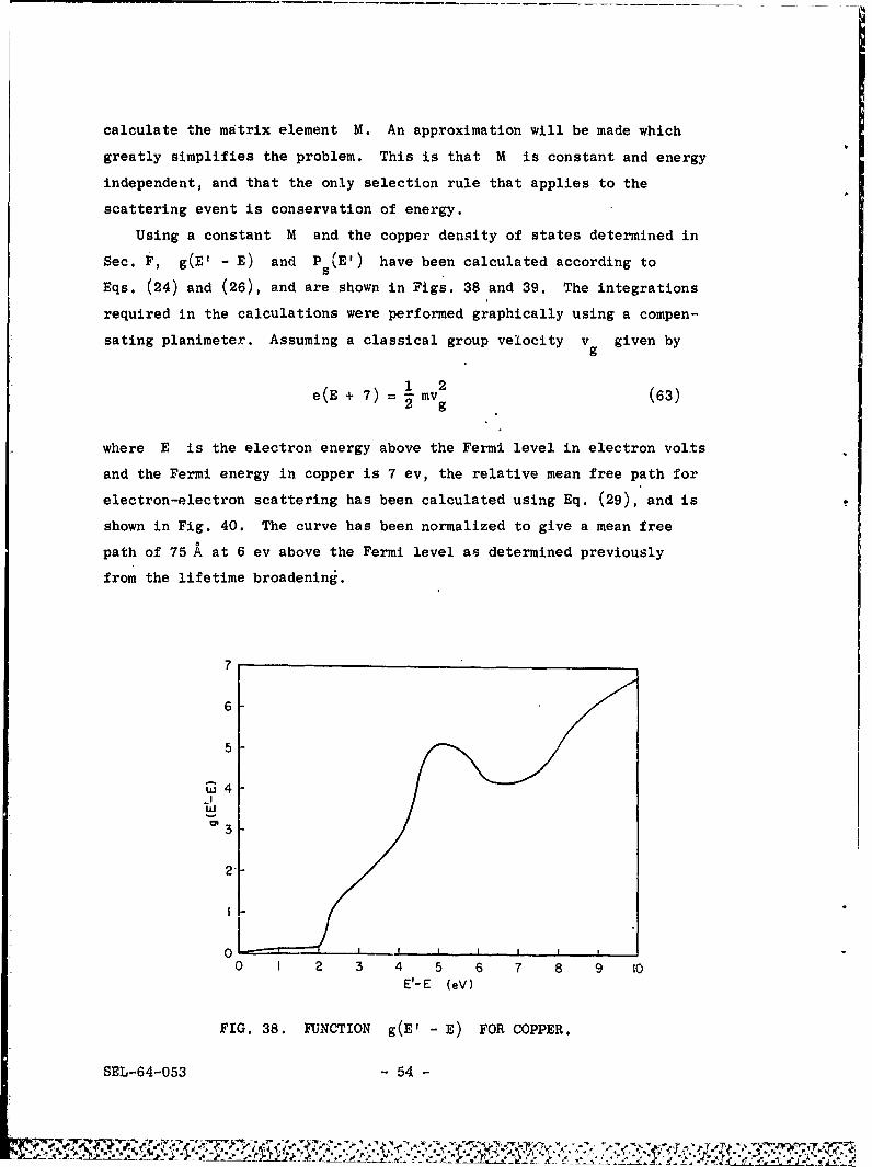
calculate the matrix element M. An approximation will be made which
greatly simplifies the problem. This is that M is constant and energy
independent, and that the only selection rule that applies to the
scattering event is conservation of energy.
Using a constant M and the copper density of states determined in
Sec. F, g(E' - E) and P (Er) have been calculated according to
Eqs. (24) and (26), and are shown in Figs. 38 and 39. The integrations
required in the calculations were performed graphically using a compen-
sating planimeter. Assuming a classical group velocity v given byg
e(E + 7) = 1 my2 (63)g (3
where E is the electron energy above the Fermi level in electron volts
and the Fermi energy in copper is 7 ev, the relative mean free path for
electron-electron scattering has been calculated using Eq. (29), and is
shown in Fig. 40. The curve has been normalized to give a mean free
path of 75 A at 6 ev above the Fermi level as determined previouslyfrom the lifetime broadening.
7
6
5
w4
2
0 1 2 3 4 5 6 7 8 9 10
E'-E (eV)
FIG. 38. FUNCTION g(E' - E) FOR COPPER.
SEL-64-053 54 -
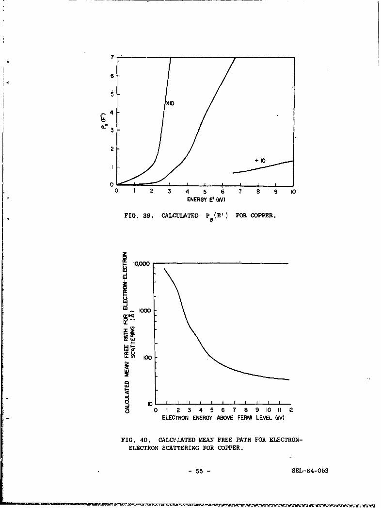
X10
-4
2
+10
00 I 2 3 4 5 6 7 a 9 10
ENERGY E' COy)
FIG. 39, CALCULATED P s(El) FOR COPPER.
100
w1-1
0w 2 3 4 7 8 9 0 111
ELCRN NRY BV FR EVLJV
IG.4.CL0LDMA REPT O LCRN
ELOTONSATRNFOCPE.
55SL6-5

Using the values of g(E' - E), Ps(E') and 2(E) in Figs. 38,
39, and 40 respectively, and the copper density of states in Fig. 33,
the energy distribution of photoemitted electrons was predicted according
to Eq. (42) at photon energies of 7.5 ev and 11.0 ev. The comparisons
between the predicted curves and the theoretical curves are shown in
Figs, 41 and, 42. The contribution of once-scattered electrons to the
curves is shown shaded to illustrate the magnitude.
The surprisingly good agreement in Figs. 41 and 42 verifies that the
low-energy peak is due to scattered electrons, and that the assumption
of constant M is reasonable. The disappointing feature of the results
is that the theory fails to predict the structurc qppearing at about
3 ev above the vacuum level in the curve of lfw = 11.0 ev. This failure
is probably due to the fact that M is not a constant; however, the
possibility that this structure is due to additional structure in the
density of states cannot be presently ruled out.
-MEASURED
-mm -CALCULATED
ONCE- SCAT-
TERED ELEC-
TRONS
Wz
0 I 2 3 4 5 6 7ELECTRON ENERGY (V)
FIG. 41. CALCULATED AND MEASURED ENERGY DISTRIBUTION
OF PHOTOEMITTED ELECTRONS--kfw = 7.5 ev.
SEL-64-053 - 56 -

-MEASURED--- CALCULATED
ONCE-SCATTEREDELECTRONS
z
O 1 2 3 4 5 6 7 8 9 toELECTRON ENERGY (eV)
FIG. 42. CALCULATED AND MEASURED ENERGY DISTRIBUTIONOF PHOTOEMITTED ELECTRONS--Kw = 11.0 ev.
Figure 43 shows energy-distribution curves at photon energies
where this peak occurs. It is evident that the peak moves to higher
energies in increments equal to the increase in h1w, and appears to
be about 4 ev lower in energy than that part of the distribution due
to excitation of d-band electrons. Referring to the density of states
of copper shown in Fig. 33, the peak appearing in Fig. 43 may be due to
electrons initially excited from the d-bands which scatter before
escaping by exciting the electrons at the top of the d-bands to the high
density of.states 1.8 ev above the.Fermi level. The energy loss involved
in this process is 4 ev, so a strong probability for this type of
scattering would result in the observed behavior. The electron excited
from the d-band by the scattering event may also escape, resulting in
the increale in yield shown in Fig. 19 in this photon energy range.
H. THE OPTICAL CONSTANTS OF COPPER
The photoemission data have shown that conservation of k-vector in
optically excited transitions is important for only a small fraction of
the optical transitions in copper. Because of this, it has been possible
to determine accurately the density of states from the bottom of the
d-bands to more than 6 ev above the Fermi level. The information on
- 57 - SEL-64-053
>
'
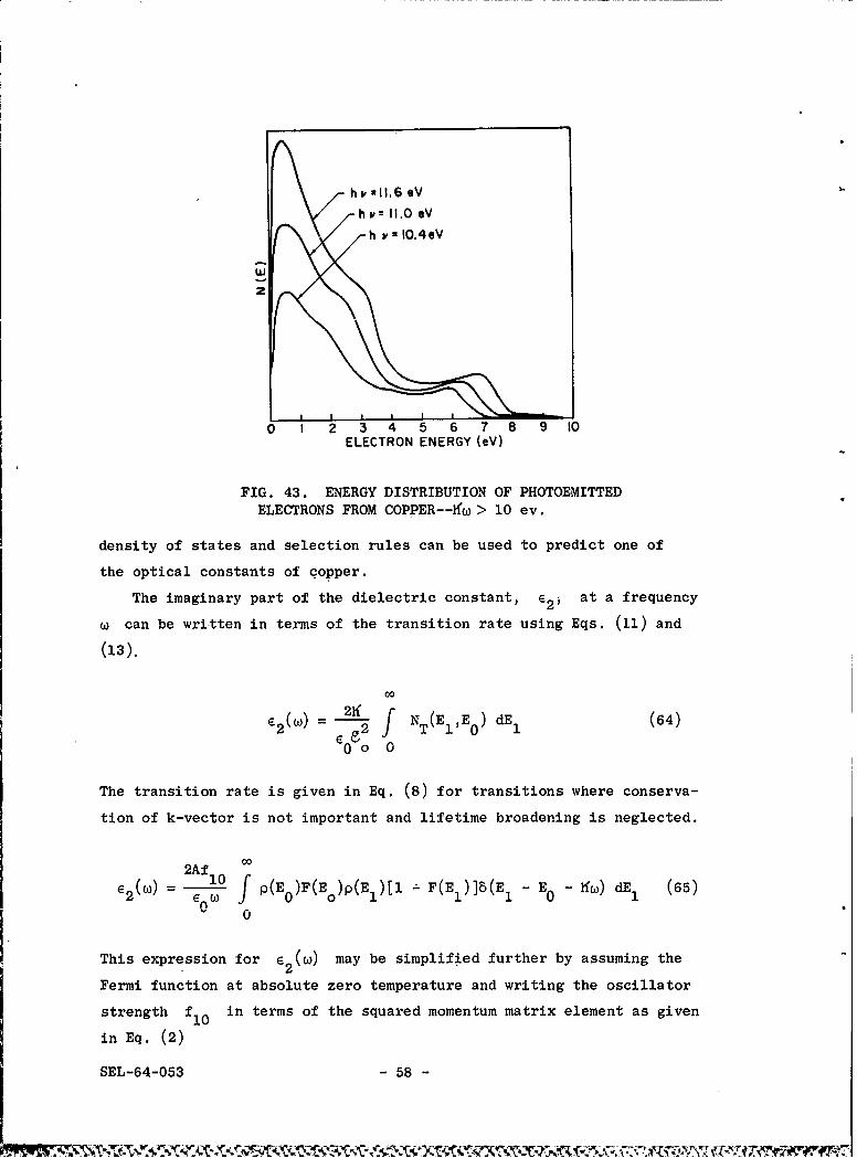
hv xII.6 eV
hP=' 11.0 eV
h 1O.4eV
Z
0 I 2 3 4 5 6 7 8 9 10ELECTRON ENERGY (eV)
FIG. 43. ENERGY DISTRIBUTION OF PHOTOEMITTED
ELECTRONS FROM COPPER--4 > 10 ev.
density of states and selection rules can be used to predict one of
the optical constants of copper.
The imaginary part of the dielectric constant, E2 at a frequency
w can be written in terms of the transition rate using Eqs. (11) and
(13).
co
000
The transition rate is given in Eq. (8) for transitions where conserva-
tion of k-vector is not important and lifetime broadening is neglected.
2Af100o= f p(E0 )F(Eo)p(E1 )[l _ F(EI)]b(El - EO _ K) dEl (65)
This expression for e () may be simplified further by assuming the2
Fermi function at absolute zero temperature and writing the oscillator
strength f10 in terms of the squared momentum matrix element as given
in Eq. (2)
SEL-64-053 - 58 -

2 EF+
6 2(w) f p(E - h&)p(El) dEl (66)me01(m0 EF
The photoemission data have shown that the squared momentum matrix
element lo 12 does not depend strongly on the energies of the initial
and final states involved in the optical transitions. It will be assumed2here that IPlo I is a constant. Although not correct in detail, such
an assumption has been shown to be a good first approximation [Ref. 14].
Under the assumption of constant momentum matrix element, Eq. (66)
can be written
E +Iiw
€2( D 2 f (E)p(E - Aw) d (07)EF
where D is a constant. The imaginary part of the dielectric constant
has been calculated from Eq. (67) using the experimentally determined
density of states. The integration involved was performed graphically
using a compensating planimeter. Curves of e 2() calculated using
the experimental data and using Burdick's density of states (Ref. 3]
are shown in Fig. 44, and are compared to e2(w) obtained by Kramers-
Kronig analysis of copper reflectance data [Ref. 19]. The calculated
curves have been normalized for best fit.
The remarkably close agreement between the calculated curves in
Fig. 44 and the curve obtained from the reflectance data indicates
that the assumption of constant momentum matrix element is a very good
approximation. It also gives further proof of the conclusion reached
directly from the photoemission data that conservation of k-vector
is not important in optically excited transitions in copper.
I. REPRODUCIBILITY OF RESULTS
Data were taken from four copper phototubes. Except for minor
differences in the sizes of peaks in the density of states, the results
from all the tubes were the same.
- 59 - SEL-64-053

N
.C EHRENREICH AND PHIILIPP
% ~CALCULATEC- EXERIMENTALZ DENSITY OF STATES
o 1.5.- i I CALCULATEC-EURDICK DENSITYOF STATES
U.,
I-
2 4 6 8 10 12 14 16PHOTON ENERGY (eV)
FIG. 44. IMAGINARY PART OF THE DIELECTRICCONSTANT e 2 FOR COPPER.
Figures 45 and 46 show energy-distribution curves for the four
tubes at photon energies of 3.9 and 5.7 ev to illustrate the differences
that did occur. At 3.9 ev, the small differences between the tubes
can be attributed to a slight difference in the threshold function
C(E). At 5.7 ev, the peaks in the d-band density of states occur at
the same energies, but the relative sizes of the peaks vary slightly
from tube to tube.
SEL-64-053 - 60 -
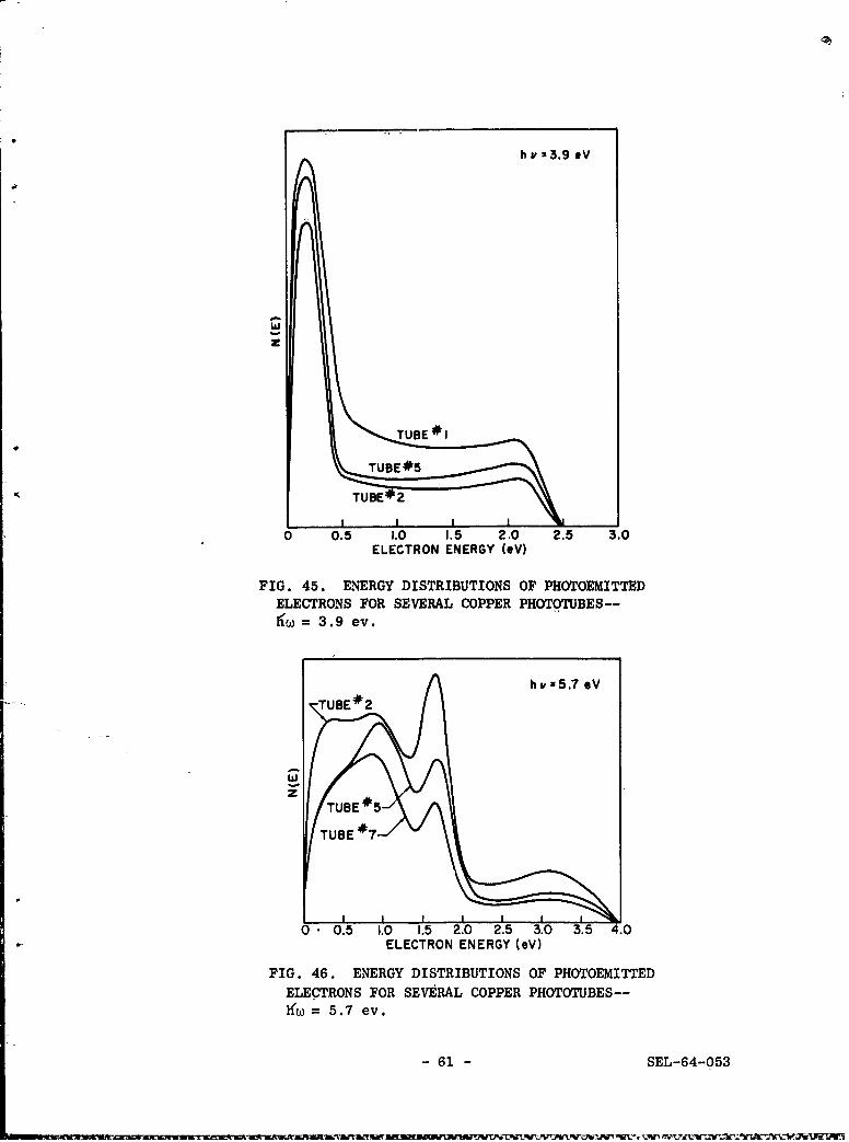
h v =3.9 eV
w
TUE
0 0.5 1.0 1.5 2.0 2.5 3.0ELECTRON ENERGY (V)
FIG. 45. ENERGY DISTRIBUTIONS OF PHOTOEMITTED
ELECTRONS FOR SEVERAL COPPER PHOTOTUBES--w= 3.9 ev.
ha' 5.7 eVTUBE*2
z TUBE #5
TUBE #7
0- 0.5 1.0 1.5 2.0 2.5 3.0 3.5 4.0ELECTRON ENERGY (eV)
FIG. 46. ENERGY DISTRIBUTIONS OF PHOTOEMITTED
ELECTRONS FOR SEVERAL COPPER PHOTOTUBES--KW = 5.7 ev.
- 61 - SEL-64-053
V. PHOTOEMISSION FROM SILVER
A. THE CALCULATED BAND STRUCTURE OF SILVER
The band structure of silver is somewhat more difficult to calculate
accu.rately than that of copper. Because of the fact that silver is a
moder,.tely heavy atom, the use of nonrelativistic atomic-wave functions
and the potential based on them will lead to more error.
Segall [Ref. 43] has calculated the band structure of silver,
ignoring relativistic effects, using two different potentials. The+
first was determined from the free ion Ag Hartree functions in the
same manner as that for copper, and the second used the Hartree-Fock
free-ion function. The results for the two fairly different potentials
were not too dissimilar, their main difference being that the d-bands
were located in different positions--2.2 ev and 5.2 ev below the Fermi
level for the Hartree and Hartree-Fock methods respectively. This
result is to be expected, since it is well known that the Hartree-Fock
orbitals are more tightly bound than the Hartree functions. The band
structure above and just below the Fermi level was very similar for the
two calculations.
From the calculations, Segall concluded that the band structure of
silver was relatively insensitive to the detai]s of the potential used
for the calculation. Knowing that the d-bands are located in silver
about 4 ev below the Fermi level, he simply shifted the d-bands in an
ad hoc way to their proper location, and assumed that all other features
of the band structure were correct. The resulting band structure is
shown in Fig. 47.
B. THE QUANTUM YIELD
Comparing the band structure of silver in Fig. 47 to that of copper
in Fig. 18, the only major difference appears to be in the location of
the d-bands. For this reason, very similar results in the quantum-yield
measurement might be expected. Referring to Fig. 48, there is no strong
similarity between the silver and copper quantum yield. The silver
yield increases from threshold to a peak at Mw 3.5 ev, then has a
SEL-64-053 - 62 -
,,. , ,

(00,0) '1,0,) (1, 00 1) (o,o0) f 0( I,0)
10
I0. A, , w; ,Z,
6 W K,a, Z8 . ,
4 Iz0\ . ,RMI LEVEL
0 AA
-2 A
-4 X6 Z W AS K
-8 -4 X K
r X W L r K X
FIG. 47. CALCULATED BAND STRUCTURE OF SILVER
10"4
10"-
--------------------------------------------- -- --- ELECTRONS/ASORBEOPI4OTON
1 4 5 6 7 a 9 10 AI 1
PHOTON ENERGY (eV)
FIG. 48. QUANTUM YIELD OF SILVER.
very sharp minimum in yield at Hf = 3.85 ev. At w = 5.6 ev, the
yield begins to increase slowly as a result of the d-band electrons
which are beginning to be excited to states above the vacuum level.
However, the increase in yield is not as great as it was in copper.
The quantum yield near threshold can be used to determine the work
function of silver (wi-th a monatomic layer of cesium on the surface) in
a manner similar to that used for copper. Figure 49 shows the square
- 63 - SEL-64-053
*~ ~ ~ _____ ____~'H~'~'~"N~ .,
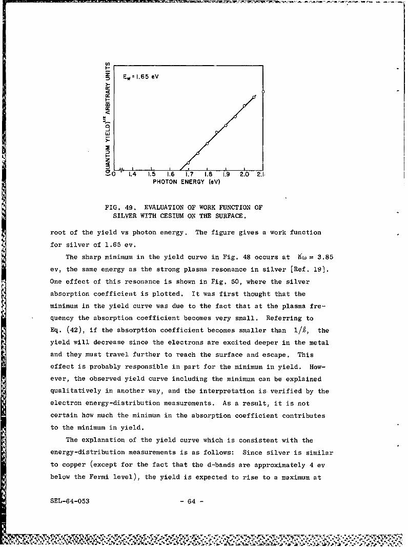
D Ew :.65 eV
n,-
CD
cJ
zD j-0 1.4 1.5 1.6 1.7 1.8 1.9 2.0 2.1-
PHOTON ENERGY (eV)
FIG. 49. EVALUATION OF WORK FUNCTION OF
SILVER WITH CESIUM ON THE SURFACE.
root of the yield vs photon energy. The figure gives a work function
for silver of 1.65 ev.
The sharp minimum in the yield curve in Fig. 48 occurs at Kiw = 3.85
ev, the same energy as the strong plasma resonance in silver [Ref. 19].One effect of this resonance is shown in Fig. 50, where the silver
absorption coefficient is plotted. It was first thought that the
minimum in the yield curve was due to the fact that at the plasma fre-
quency the absorption coefficient becomes very small. Referring to
Eq. (42), if the absorption coefficient becomes smaller than 1/2, the
yield will decrease since the electrons are excited deeper in the metal
and they must travel further to reach the surface and escape. This
effect is probably responsible in part for the minimum in yield. How-
ever, the observed yield curve including the minimum can be explained
qualitatively in another way, and the interpretation is, verified by the
electron energy-distribution measurements. As a result, it is not
certain how much the minimum in the absorption coefficient contributes
to the minimum in-yield.
The explanation of the yield curve which is consistent with the
energy-distribution measurements is as follows: Since silver is similar
to copper (except for the fact that the d-bands are approximately 4 ev
below the Fermi level), the yield is expected to rise to a maximum at
SEL-64-053 - 64 -
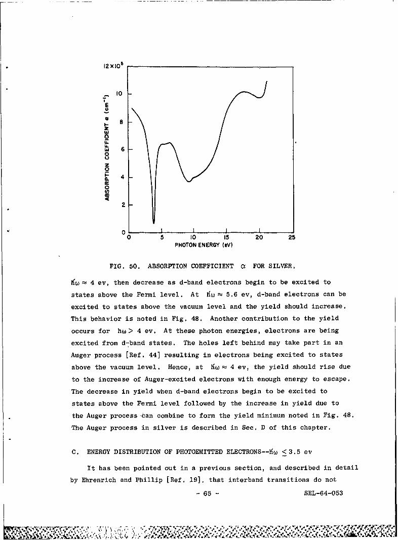
12 X 10
10T
E
zw
IA.w 60.
z0
40
2
0 5 10 15 20 25PHOTON ENERGY (V)
FIG. 50. ABSORPTION COEFFICIENT a FOR SILVER.
Kw 4 ev, then decrease as d-band electrons begin to be excited to
states above the Fermi level. At w 5.6 ev, d-band electrons can be
excited to states above the vacuum level and the yield should increase.
This behavior is noted in Fig. 48. Another contribution to the yield
occurs for hw > 4 ev. At these photon energies, electrons are being
excited from d-band states. The holes left behind may take part in an
Auger process [Ref. 44) resulting in electrons being excited to states
above the vacuum level. Hence, at Aw 1 4 ev, the yield should rise due
to the increase of Auger-excited electrons with enough energy to escape.
The decrease in yield when d-band electrons begin to be excited to
states above the Fermi level followed by the increase in yield due to
the Auger process can combine to form the yield minimum noted in Fig. 48.
The Auger process in silver is described in Sec. D of this chapter.
C. ENERGY DISTRIBUTION OF PHOTOEMITTED ELECTRONS--Aw < 3.5 ev
It has been pointed out in a previous section, and described in detail
by Ehrenrich and Phillip [Ref. 19), that interband transitions do not
- 65 - SEL-64-053
AM ~~~A v 7 SV
11Y ?sXArjA.

become dominant in silver until iw > 3.5 ev. The energy distribution
of photoemitted electrons from silver for iw < 3.5 ev shown in Fig. 51
demonstrates this. A peak near the maximum electron energy becomes more
apparent as 46b increases, but does not dominate the distribution.
This peak is due to indirect transitions from the peak in the density
of states at L2 in the calculated band structure (Fig. 47). The
remainder of the distribution curves is due to the characteristic"free" electron contribution.
The peak near the maximum electron energy for hw < 4.0 ev follows
the relation
E = 1iW - 1.95 ev (68)
where E is the energy of the peak with respect to the vacuum level.
Since the work function of silver is 1.65 ev, the peak in the energy
distributions is due to a peak in the density of states at L2' located
0.3 ev below the Fermi level. Figure 51 indicates that a larger peakin the density of states is associated with symmetry point L t in
2silver than in copper.
In the photoemission data of silver, there is no evidence of a peak
in the density of states at X ' 1 .8 ev above the Fermi level, as has
4
0 0 I0 1.5 2.0£LCTRON ENERGY (ev)
FIG. 51. ENERGY DISTRIBUTION OF PHOTOEMITTEDELECTRONS FROM SILVER--liw 3.5 ev.
SEL-64-053 - 66 -
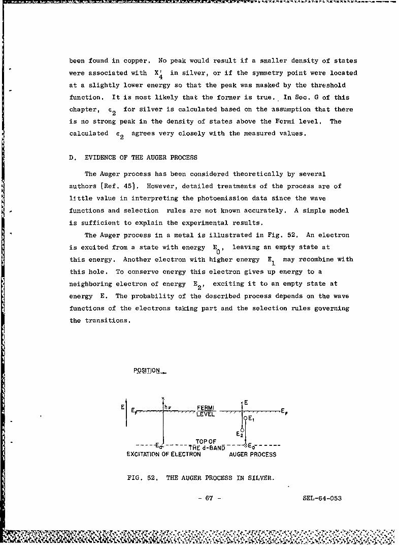
been found in copper. No peak would result if a smaller density of states
were associated with X in silver, or if the symmetry poin't were located
at a slightly lower energy so that the peak was masked by the threshold
function. It is most likely that the former is true. In Sec. G of this
chapter, e2 for silver is calculated based on the assumption that there
is no strong peak in the density of states above the Fermi level. The
calculated e2 agrees very closely with the measured values.
D. EVIDENCE OF THE AUGER PROCESS
The Auger process has been considered theoretically by several
authors [Ref. 45]. However, detailed treatments of the process are of
little value in interpreting the photoemission data since the wave
functions and selection rules are not known accurately. A simple model
is sufficient to explain the experimental results.
The Auger process in a metal is illustrated in Fig. 52. An electron
is excited from a state with energy E0 , leaving an empty state at
this energy. Another electron with higher energy E1 may recombine with
this hole. To conserve energy this electron gives up energy to a
neighboring electron of energy E2, exciting it to an empty state at
energy E. The probability of the described process depends on the wave
functions of the electrons taking part and the selection rules governing
the transitions.
P.OSITION.
xEE hFERMI
ELEVEL Ejh;EF
TOP OF.... '- . .. RE d-BAND .... ,07
EXCITATION OF ELECTRON AUGER PROCESS
FIG. 52. THE AUGER PROCESS IN SILVER.
- 67 - SEL-64-053
jmvrr
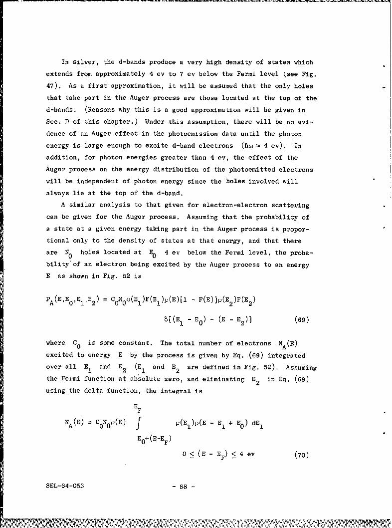
In silver, the d-bands produce a very high density of states which
extends from approximately 4 ev to 7 ev below the Fermi level ksee Fig.
47). As a first approximation, it will be assumed that the only holes
that take part in the Auger process are those located at the top of the
d-bands. (Reasons why this is a good approximation will be given in
Sec. D of this chapter.) Under this assumption, there will be no evi-
dence of an Auger effect in the photoemission data until the photon
energy is large enough to excite d-band electrons (h& - 4 ev). In
addition, for photon energies greater than 4 ev, the effect of the
Auger process on the energy distribution of the photoemitted electrons
will be independent of photon energy since the holes involved will
always lie at the top of the d-band.
A similar analysis to that given for electron-electron scattering
can be given for the Auger process. Assuming that the probability of
a state at a given energy taking part in the Auger process is propor-
tional only to the density of states at that energy, and that there
are N holes located at E0 4 ev below the Fermi level, the proba-
bility of an electron being excited by the Auger process to an energy
E as shown in Fig. 52 is
P A (E, E 0E ) = C0N 0O(E )F(E )p(E)[l - F(E)]p(E 2)F(E 2)
-(E1 E0 ) - (E - E2 )] (69)
where C is some constant. The total number of electrons N A(E)
excited to energy E by the process is given by Eq. (69) integrated
over all E1 and E2 (E1 and E2 are defined in Fig. 52). Assuming
the Fermi function at absolute zero, and eliminating E2 in Eq. (69)
using the delta function, the integral is
E F
NA(E) = C0N0 (E) f p(E1 )P(E - E1 + E0 ) dEl
E0+ (E-EF)
0 < (E - EF) < 4 ev (70)
SEL-64-053 - 68 -
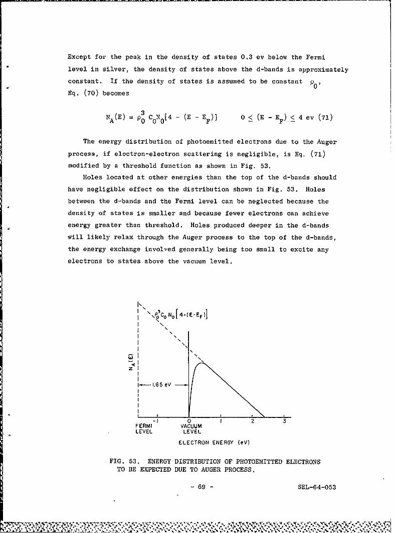
Except for the peak in the density of states 0.3 ev below the Fermi
level in silver, the density of states above the d-bands is approximately
constant. If the density of states is assumed to be constant p10
Eq. (70) becomes
NA(E) = p0 CoN 0 (4 - (E - EF)) 0 < (E - EF) < 4 ev (71)
The energy distribution of photoemitted electrons due to the Auger
process, if electron-electron scattering is negligible, is Eq. (71)
modified by a threshold function as shown in Fig. 53.
Holes located at other energies than the top of the d-bands should
have negligible effect on the distribution shown in Fig. 53. Holes
between the d-bands and the Fermi level can be neglected because the
density of states is smaller and because fewer electrons can achieve
energy greater than threshold. Holes produced deeper in the d-bands
will likely relax through the Auger process to the top of the d-bands,
the energy exchange involved generally being too small to excite any
electrons to states above the vacuum level.
\ \Co No[-(E-EF)I
\0 1
N
I-1.65 eV
FERMI VACUUM
LEVEL LEVEL
ELECTRON ENERGY (eV)
FIG 53 ENRGYDISTRIBUTION OF PHOTOEMITTED ELECTRONSTBE EXPECTED DUE TO AUGER PROCESS.
69 -SEL-64--053
%
I !4

Figure 53 indicates that the Auger process will result in an energy
distribution of electrons decreasing with energy to a maximum energy of
approximately 2.4 ev above the vacuum level. Figure 54 shows the experi-
mentally determined energy distribution curves for silver for photon
energies of 4.1, 4.3, 4.8, and 5.4 ev. The distributions have been
normalized to coincide at low energies. Figure 55 shows the energy
distributions at photon energies of 3.6, 3.8, and 4.0 ev. Except for
the high-energy peak associated previously with a peak in the density
of states 0.3 ev below the Fermi level, the energy distributions shown
in Figs. 54 and 55 are very similar to the distributions predicted on
h-4eV
, ~v 4 30
hl5.4 4V
ELECTRON ENERGY (V)
FIG. 54. ENERGY DISTRIBUTION OF PHOTOEMITTED
ELECTRONS FROM SILVER--iw = 4.1 ev to 5.4 ev.
h,, 3.6 Wj
I h v',-4.0 eV,-
0, 0.s 1!0 t5 2.0 2.5
ELECTRON ENERGY (IV)
FIG. 55. ENERGY DISTRIBUTION OF PHOTOEMITTEDELECTRONS FROM SILVER--w NEAR THE PLASMAFREQUENCY.
SEL-64-053 - 70 -
|L

the simple model of the Auger process. A low-energy peak due to the
Auger process begins to appear when the photon energy is approximately
4 ev, and the distribution at higher photon energies is essentially
independent of photon energy, extrapolating to an energy of 2.5 ev as
shown in Fig. 54.
The broad peak in Fig. 54 6,c ted between 1.5 ev and 2.5 ev can be
explained in terms of the peak in the density of states at L2' A very
probable event is for electrons near L' to recombine with holes at the
top of the d-band, energy being given up to neighboring electrons also
near L2 . The energies are such that this process will result in a
peak approximately 1.8 ev above the vacuum level.
The simple model for the Auger process that has been used also
explains why the process is negligible in copper. Since the d-bands
in copper are only 2 ev below the Fermi level, a negligible fraction of
the Auger-excited electrons is excited to energies above the vacuum
level.
E. INDIRECT AND DIRECT TRANSITIONS IN SILVER
The high-energy peak in the electron energy distributions in Fig.
54 exhibits the same behavior as that noted for the similar peak in
copper. At a photon energy of approximately 4.1 ev, the peak is a
maximum, and at higher photon energies it splits into two peaks. One
of the peaks moves to higher energy in increments equal to the change
in photon energy, while the other moves to higher energy at a somewhat
slower rate. The amplitudes of the peaks get smaller as the peaks are
excited to high energies because of strong energy-dependent scattering.
The peaks in the energy distributions can be explained in terms of
direct and indirect transitions in the same way as the similar peaks
were explained in copper. Figure 56 shows the energy of the iniotial
states responsible for the largest peak in the distributions of Fig. 54
plotted vs Kw. The peak is due to indirect transitions from the peak
in the density of states at L2 for photon energies less than 3.5 ev.
From the figure, it is evident that L2 is located 0.3 ev below the2
Fermi level. At w = 3.5 ev, the direct transition is beginning to
contribute. The initial states involved in the direct transition lie
- 71 - SEL-64-053
"Ai

hi, (eV)
0 .2 3 4 5 6VII I I
-01
-0.2- 0
-03-
-0.4-
- 0.5
-0 6
-0.7-
-0 8
FIG. 56. ENERGY OF INITIAL STATES RESPONSIBLEFOR HIGH-ENERGY PEAK IN PHOTOEMISSION DATA.
above L" for 3.5 < 1v < 4.2 ev. As a result, the curve in Fig. 562
goes through a maximum at h'&= 4.0 ev. At h', = 4.2 ev, the transition
is -.Z"rring again from initial states at L2, 0.3 ev below the Fermi
level. jince the peak at H,, = 4.2 ev is due to direct transitions
from L' to L1, L1 is located 3.9 ev above the Fermi level.
F. TRANSITIONS FROM THE d-BANDS
Since the d-bands in silver are located approximately 4 ev below
the Fermi A-vel, at photon energies greater than 5.7 ev, d-band elec-
trons should be excited to states above the vacuum level. Figure 57
shows the electron energy distributions from silver for photon energies
of 5.7 ev and 6.3 ev. At 5.7 ev there is no evidence of d-band elec-
trons in the distribution, but at 6.3 ev a low-energy peak appears
which is due to transitions from the d-bands. The energy distributions
at li. = 7.8 ev and 8.4 ev are shown in Figs. 58 and 59. The narrow
peak in the distributions is due to a peak in the d-band density of
states, and the peak following the first peak at approximately 1 ev
lower energy is also due to the d-bands. The low-energy peak appearing
in the curve at l1w = 7.8 ev, and more strongly in the curve at
h.,= 8.4 ev, is due to scattering.
SEL-64-053 - 72 -
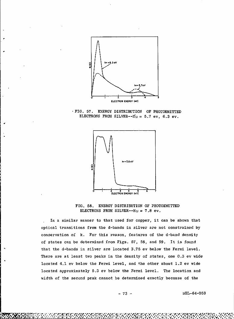
hy 6.3 eV
h 5,7eV
0 I 2 3 4 5
ELECTRON ENERGY (OV)
.FIG. 57. ENERGY DISTRIBUTION OF PHOTOEMITTEDELECTRONS FROM SILVER-- = 5.7 ev, 6.3 ev.
-Lhy -7.8 OV
0 I 2 3 4 5 6 7ELECTRON ENERGY (OV)
FIG. 58. ENERGY DISTRIBUTION OF PHOTOEMITTED
ELECTRONS FROM SILVER--Hw. = 7.8 ev.
In a similar manner to that used for copper, it can be shown that
optical transitions from the d-bands in silver are not constrained by
conservation of k. For this reason, features of the d-band density
of states can be determined from Figs. 57, 58, and 59. It is found
that the d-bands in silver are located 3.75 ev below the Fermi level.
There are at least two peaks in the density of states, one 0.3 ev wide
located 4.1 ev below the Fermi level, and the other about 1.2 ev wide
located approximately 5.3 ev below the Fermi level. The location and
width of the second peak cannot be determined exactly because of the
- 73 - SEL-64-053

i h.' 8.4 ev
0 I 2 3 4 5 0 7ELECTRON ENERGY (eV
FIG. 59'. "NERGY' DISTRIBUTION OF PHOTOEMITTED
ELECTRONS FROM SILVER-, = 8.4 ev.
masking due to scattered electrons. When the magnitude of the scattered
peak is estimated using Eq. (42) and subtracted from the distributions
shown in Figs. 58 and 59, there is no evidence of further structure in
the d-bands. Because of this, it is likely that the silver d-band
density of states consists of only the two peaks mentioned above.
G. THE SILVER DENSITY OF STATES
The density of states of silver is considerably more difficult to
determine exactly from the photoemission data than that of copper.
At photon energies less than 3.5 ev, the electron energy distributions
are dominated by the free electron effects: at photon energies between
3.8 ev and 6.5 ev, the distributions are dominated by the Auger effect;
and at photon- energies above 7.0 ev, the distributions are distorted
badly due to scattering. However, several important features of the
density of states can be determined. The location and density of states
of part of the d-band can be estimated, and two peaks in the density of
states identified. The only other evidence of structure in the density
of states is the peak at L' 0.3 ev below the Fermi level. From
these considerations, a silver density of states has been estimated and
is shown in Fig. 60. The accuracy of the density of states in Fig. 60
is not as good as that for copper. However, the general features are
correct as indicated in Fig. 61 where the imaginary part of the dielectric
SEL-64-053 - 74 -

UI
U)
LJ
I-
0
I-.
z
L
-8 -6 -4 -2 0 2 4 6 8 10 12
ENERGY-FERMI ENERGY (eV!
FIG. 60. ESTIMATED DENSITY OF STATES FOR
SILVER.
1.5 - EHRENREICH AND PHILIPP---- CALCULATED - EXPERIMENTAL
DENSIYY OF STATES
z
uI.
i\
to
U
0 2 4 6 a 10 12 14PHOTON ENERGY (IV)
FIG. 61. IMAGINARY .PART OF THE DIELECTRIrCCONSTANT e2 FOR SILVER.
- 75 - SEL-64-053
, /'.,;%TF, . . ?.-, " . '.? .Y ,K ..- '- , , v,. ." L" ; ;'':''""7- € ' T-'--"; 0-- '
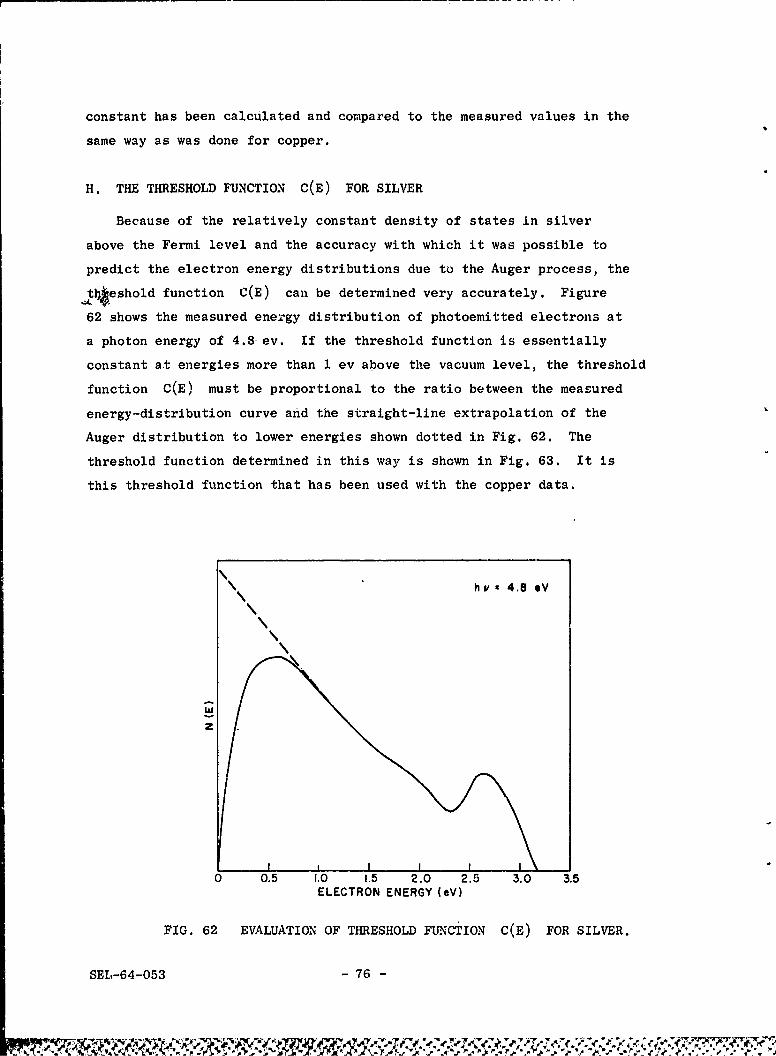
constant has been calculated and compared to the measured values in the
same way as was done for copper.
H. THE THRESHOLD FUNCTION C(E) FOR SILVER
Because of the relatively constant density of states in silver
above the Fermi level and the accuracy with which it was possible to
predict the electron energy distributions due to the Auger process, the
t4eshold function C(E) can be determined very accurately. Figure
62 shows the measured energy distribution of photoemitted electrons at
a photon energy of 4.3-ev. If the threshold function is essentially
constant at energies more than 1 ev above the vacuum level, the threshold
function C(E) must be proportional to the ratio between the measured
energy-distribution curve and the straight-line extrapolation of the
Auger distribution to lower energies shown dotted in Fig. 62. The
threshold function determined in this way is shown in Fig. 63. It is
this threshold function that has been used with the copper data.
h v x 4.0 eV
z
0 0.5 1.0 1.5 2.0 2.5 3.0 3.5ELECTRON ENERGY We)
FIG. 62 EVALUATION OF THRESHOLD FUNCTION C(E) FOR SILVER.
SEL-64-053 -76-
W Z'_1XZz -6A\

W
Z
LJ
Z
U.
0
I-
0 .2 .4 .6 .8 1.0 1.2 1.4ENERGY ABOVE THRESHOLD (eV)
FIG. 63. THRESHOLD FUNCTION C(E)FOR SILVER.
I. EFFECT OF ELECTRON-ELECTROIN SCATTPERING
Electron-electron scattering in silver affects the photoemission
data in a similar way to that in copper. Figure 54 shows the high-
energy peak in the energy distribution being reduced in size as the
peak is excited to higher energy, but the quantum yield in this photon-
energy range is relatively constant. One would expect that, since
direct transitions Lre beginning to occur, the height of the peak should
increase rather than decrease. The observed behavior is due to the fact
that the mean free path is a decreasing function of energy, and the
probability of escape without scattering of a high-energy electron is
correspondingly smaller than that of a lower energy electron. Figures
58 and 59 show the low-energy peak in the energy distribution which is
due to the scattering of high-energy electrons. Figures 64 and 65 are
the energy distributions of photoemitted electrons from silver at photon
energies of 9.3, 10.5, and 11.4 ev, and show the lifetime broadening of
the high-energy d-band peak (labeled C).
77 -SEL-64-053
Oxy 5 "i 0 R "-W .l

hv , 10.5 iV
C
hv 9.3 eV
0 3 4 5 6 7 8 9ELECTRON ENERGY (eV)
FIG. 64. ENERGY DISTRIBUTION OF PHOTOEMITTED ELECTRONSFROM SILVER--K1 > 9 ev.
z
ELECTRON ENERGY (Nv)
FIG. 65. ENERGY DISTRIBUTION OF PHOTOEMITTED ELECTRONSFROM SILVER--hw = 11.4 ev.
The mean free path at one energy can be estimated from the lifetime
broadening of the sharp d-band peak in silver. This has been done in
the same way as was done for copper in Sec. Gi of Chapter IV, but using
a Fermi energy of 5.5 ev [Ref. 41). The estimated mean free path for
electron-electron scattering at 5.5 ev above the Fermi level is 70 A.Since it was not possible to determine the density of states in
silver with the accuracy achieved with copper, no detailed calculations
of I(E), ps(E,E), and PS(E') were carried out. However, several
of the important features of the scattering and their effect on the
SEL-64-053 - 78 -
"R

energy distribution of photoemtted electrons can be described without
detailed calculations.
There is a high density of states in silver in the d-band approxi-
mately 4 ev below the Fermi level. When electrons have enough energy
to scatter with these d-electrons and excite them to states above the
Fermi level, there will be a large probability for scattering (short
electron-electron mean free path). Referring to Fig. 54, it can be
seen that strong scattering begins to reduce the size of the high-energy
peak in the energy-distribution curves when the peak corresponds to
electron energies more than 2.3 ev above the vacuum level, or 3.95 ev
above the Fermi level, in close agreement with the intuitive argument.
In addition, since the density of states in silver is relatively con-
stant above the Fermi level, no structure in the scattering peak similar
to that appearing in Fig. 43 for copper is to be expected, and none is
observed (see Fig. 65).
J. EFFECT OF THE PLASMA RESONANCE AT ft = 3.85 ev
The plasma frequency at hw = 3.85 ev in silver may affect the
photoemission data in several ways. The decrease in yield at incident
light frequencies near the plasma frequency which can be brought about
by a decrease in the absorption coefficient has already been described.
It might be expected that a further decrease in yield should result
because photons absorbed in producing plasma oscillations do not directly
produce photoelectrons. However, if photoelectrons are produced by the
relaxation of these plasma oscillations, this effect will not occur.
A further effect of the plasma resonance in silver has been mentioned
briefly in Chapter IIB. Energetic electrons may lose energy in traveling
through the metal by exciting plasma oscillations. In this scattering
mechanism, the energy loss per scattering event is approximately equal
to the energy corresponding to the plasma frequency. Hence, if this
scattering process were strong in silver, there would be a large
the photoemission data, this would result, for instance, in a strong
scattered peak in the energy-distribution curves following by 3.85 ev
the sharp peak in the distributions due to optical excitation of electrons
- 79 - SEL-64-053
,~.e''P,. -A

from the top of the d-band. Since no such structure is observed in the
energy-distribution curves of silver, it is concluded that scattering
of energetic electrons by the creation of plasma oscillations is a weak
scattering process compared to electron-ele'ctron scattering over the
range of electron energy studied. This conclusion is in agreement with
the theoretical results of Quirhn ('Ref. 6].
SEL-64-053 - 80 -
42-

VI. DISCUSSION AND CONCLUSIONS
One of the most significant features of the experimental results
is the evidence that conservation of k-vector in most optically excited
transitions is not important in copper and silver. For transitions
from the s- and p-like bands just below the Fermi level, this behavior
is not unexpected since the same mechanism that conserves k-vector in
the "free carrier" absorption referred to in the literature [Ref. 19]
may be expected to do so for these transitions. However, when the
photon energy is such that a strong direct transition should occur,
direct transitions are observed, but it is found that the direct transi-
tions are not as strong as the indirect transitions. In addition, no
evidence is found for direct transitions from the d-bands.
There are several possible explanations for the observed behavior.
The second-order transition probability involving phonons [Eq. (9)] may
be large enough in the metals to result in indirect transitions being
stronger than direct transitions. This behavior may occur even if the
second-order matrix element is smaller than the first-order matrix
element because of the larger number of electrons available to take
part in phonon-assisted transitions. However, measurements of the
quantum yield per incident photon of a copper phototube from threshold
to hw = 3.5 e, at room temperature and at 770 K, showed no noticeable
difference in yield. If phonons were strongly involved in the transi-
tions, a change in yield-would have occurred.
Another possible explanation for the observations is that a large
probability exists for some other mechanism such as defects [Ref. 46]
to conserve k-vector. This mechanism would not be expected to have a
strong temperature dependence in agreement with the yield measurements
at roop temperature and at 770 K.
There is the additional possibility that the Bloch-wave representa-
tion of some of the electronic states in copper and silver may not be
adequate [Refs. 22, 23]. In particular, this may be true for the d-band
states because of the fact that no evidence of direct transitions from
the d-bands was found. This possibility cannot be ruled out on the basis
of the close agreement between the measured density of states and that
- 81 - SEL-64-053
12

calculated assuming Bloch-wave solutions for the wave equation [Ref. 3).
The density of states if the Bloch-wave representation is not correct
will be very similar to that calculated using the Bloch-wave representa-
tion because the density of states is much more dependent on the crystal
potential than on the representation of the wave function.
The experimental results of the photoemission study can be used to
compare th6 metals copper and silver. It has already been mentioned
that k-vector conservation is not a strong selection rule in either of
the metals for many optical transitions. The band structure and density
of states of both are very similar, the major difference being that the
d-bands are located 4 ev below the Fermi level in silver and 2 ev below
the Fermi level in copper. Both have two peaks in the d-band density
of states, a sharp peak near the top of the band and a broader peak
deeper in the band, and both d-bands are approximately 3.5 ev wide. The
p- and s-like bands above and just below the Fermi level appear to be
similar. The symmetry points L' and L differ in energy by less2 1than 0.2 ev. However, the difference between copper and silver in the
density of states at L' and the difference in the way in which the
effect of the direct transition from L' to L1 varies with photon
energy (Figs. 28 and 56), in addition to the lack of evidence of a peak
in the silver density of states at X4, indicate that the shape of
the bands in the two metals is somewhat different. These results bear
out Segall's conclusion [Ref. 44) that the band structure of silver is
very similar to that of copper, the only major difference being that
the d-bands are moved to a lower energy 4 ev below the Fermi level.
Electron-electron scattering is the strongest inelastic-scattering
mechanism in both silver and copper for electrons with energies from
1.5 ev to 11.5 ev above the Fermi level. There is no evidence of
scattering due to plasmon creation. The mean free path for electron-
electron scattering for copper is a decreasing function of electron
energy. From lifetime-broadening considerations a value of approximately
75 A is found for the mean free path against this scattering for electrons6 ev above the Fermi surface. The mean free path for silver appears to
be a more sharply decreasing function of electron energy, and is slightly
shorter than that for copper at energies more than 5 ev above the Fermi
level.
SZL-64-053 - 82 -
The close agreement between the calculated imaginary part of the
dielectric constant e2 (based on the experimental observation) and
the measured e2 indicates that the observations are not peculiar to
the photoemission process, but are characteristic of the metals
studied.
It was possible to explain the photoemission data from both copper
and silver in detail. In particular, it was possible to predict with
considerable accuracy the energy distribution of photoemitted electrons
to be expected at any photon energy from 1.5 to 11.5 ev. It should be
pointed out, however, that total agreement between the predicted and
the measured distributions could have been achieved by slight changes
in the densities of states and matrix elements involved in the transi-
tions. Such adjustments in the data were not made in order to illustrate
the ease and accuracy with which photoemission results can be interpreted,
and to indicate the vast amount of information that can be gained with-
out a detailed analysis.
- 83 - SEL-64-053
W I 'r

APPENDIX A. PROBABILITY OF ELECTRON ESCAPE AFTER ONE SCATTERING EVENT
The probability of an electron with energy E a distance x from
a photoemitting surface escaping into vacuum without suffering an
inelastic collision has been derived in Sec. Cl of Chapter II. The
probability of this electron escaping after scattering once is also
of interest.
Consider an electron excited to energy E' a distance x from
the photoemitting surface, as shown in Fig. 66. The probability of this
electron escaping with energy between E and (E + dE) is the product
of three probabilities:
1. The probability that it will scatter after moving a distance r
in the solid at an angle e with respect to the normal to the
photoemitting surface.
2. The probability that it will be scattered to an energy between
E and (E + dE).
3. The probability that it will escape after this scattering eventwithout further scattering.
Referring to Fig. 66, the first probability, assuming random electron
velocity direction, is
1 -r/s' dr (72)P1 = e sin de-
where ' is the mean free path for inelastic scattering for electrons
with energy E'. The probability of producing an electron with energy
between E and (E + dE) in the scattering event was derived in
Chapter IID.
2ps(E',E) dE
P2 - P (E')s
The third probability is given by Eq. (31), where the distance of the
electron from the photoemitting surface is (x - r cos 0).
1
P 3 = f exp(x + r cos dz (74)
Pc /p~
SEL-64-053 - 84 -
%i
Changing variables so that y = cos e, and integrating Eq. (75) over
r gives
ec(El E (E',E)dE f 1 df z
ese ~ ~~~ ~ ~ 2P E2)zE='dyf d-1 pc/p Z -z
+ dy f dz 1_ _ y_
0 pc/p T &z
(76)
Electrons are optically excited to energy E' according to Eq. (32),
so the rate of escape of electrons with energy between E and '(E + dE)
is
00
R'(EtE) dE f (G0 (E')e-C Xp ' (E',E) dE] dx (77)
0
Substituting Eq. (76) in Eq. (77) and carrying out the integration over
x gives
R'(E',E) dE G 0 (Ips E,) 0dy f dz12PPs f f - - +(Et
1c/ 11 F ~
+fdyf dz (7 7 (78)
Simplifying Eq. (78) and performing the y integration, one obtains
SEL-64-053 - 86 -

Changing variables so that y = cos 0, and integrating Eq. (75) over
r gives
pe(E',E,x) dE s f dy f dz 1 - zec2 Ps (E' ) f _
- p ' z
1 1 -exp + 2s- exp -
+ dyf dz 12y
0 pc/p z
(76)
Electrons are optically excited to energy E' according to Eq. (32),
so the rate of escape of electrons with energy between E and I(E + dE)
is
O
R'(E',E) dE =f [G 0 (E')e--a p I E',E) dE] dx (77)
0
Substituting Eq. (76) in Eq. (77) and carrying out the integration over
x gives
RG(E',E) dE = (E')p s(E',E) dE 0 dzs -i ~~pc/p v- +T
1 dz I/y (78)
Simplifying Eq. (78) and performing the y integration, one obtains
SEL-64-053 - 86 -
RG(E',E) dE 0- ( + )
2Ps (E') fC
\I dz
; n +z -(79)
.z
This integration may be carried out exactly, but the result is rather
difficult to interpret. A considerable simplification can be made
with very little loss in accuracy as follows: The major contribution
to the integral occurs for z near unity. Since in metals i' is
generally shorter than A, and x An (l + (l/x)] is a very slowly
varying function of x for x large, very little error is introduced
by inserting z = 1 in the Az/' An [1 + (P'/iz)] term of Eq. (79).
Under this approximation, Eq. (79) becomes, from Eq. (35),
R'(E',E) dE = K0 ) A An (1 + a ') + LT n +Ps(,)( + . Tit
(80)
For a ' and A'/A much less than unity, [I/ai']n (1 + ai') =12
[A/P')An [1 + (2'/2)] and Eq. (80) gives the same result as derived in
Eq. (42) using the very simple model.
The expression given in Eq. (80) for the rate of escape of elec-
trons after scattering once is easily interpreted. The (A/ ')in [1+1'/I]
term represents those electrons initially excited to energy E' which
are moving away from the photoemitting surface. These electrons eventually
will be scattered regardless of the value of the mean free path for
scattering, and their probability of escaping after scattering once will
depend on the ratio of the mean free paths 2/2'. This interpretation
suggests that inelastic scattering will always affect photoemission data
irrespective of the mean free paths. The (l/ai') An (1 + aA') term
represents those electrons initially excited to energy E' which are
moving toward the photoemitting surface. The probability of these
electrons escaping after scattering once will depend on the probability
of their scattering once before reaching the surface. If 2' >> 1/a,
most of these electrons will escape without scattering. If A' << 1/a,
few will escape without scattering.
- 87 - SEL-64-053
N't SA .
23. W. E. Spicer, Ohys. Rev. Lett., 11, 1963, p. 1-3.
24. W. E. Spicer and N. B. Kindig, Solid State Communications, 2, 1964,p. 13.
25. L. H. Hall, J. Bardeen, and F. J. Blatt, Phys. Rev., 95, 1954,p. 559.
26. K. Sawada, et al, Phys. Rev., 108, 1957, p. 507.
27. E. 0. Kane, Phys. Rev., 127, 1962, p. 131.
28. C. Kittel, Introduction to Solid State Physics, John Wiley and
Sons, Inc., New York, 1960.
29. W. E. Spicer, J. Appl. Phys., 31, 1960, p. 2077.
30. R. N. Stuart, F. Wooten, and W. E. Spicer, Phys. Rev. Lett., 10,
1963, p. 1-3.
31. C. Kittel, Elementary Solid State Physics, John Wiley and Sons,
Inc., New York, 1962, p. 112.
32. F. I. Vilesov, Soviet Physics, 6, 1962, p. 1078.
33. W. E. Spicer, J. Phys. Chem. Solids, 22, 1961, p. 365.
34. W. E. Spicer, personal communication.
35. B. Kindig, "Photoemission Studies of CdS," to be published.
36. ohn and N. Rostoker, Phys. Rev., 94, 1954, p. 1111.
37. M. Ch ow, Phys. Rev., 55, 1939, p. 675; Ph.D. Thesis, M.I.T.,1939, ku.,,Vublished).
38. J. C. Slater, Phys. Rev., 51, 1937, p. 846; Phys. Rev., 92, 1953,p. 603.
39. L. P. Bouckaert, R. Smoluchowski, and E. Wigner, Phys. Rev., 50,
1936, p. 58.
40. R. H. Fowler, Phys. Rev., 38, 1931, p. 45.
41. A. J. Dekker, Solid State Physics, Prentice-Hall, Inc., N. J.,1957, p. 215.
42. C. A. Mead, personal communication.
43. B. Segall, "Theoretical Energy Band Structures for the NobleMetals," Report No. 61-RL-(2785G), General Electric ResearchLaboratory, Schenectady, N. Y., Jul 1961.
44. J. Blakemore, Semiconductor Statistics, Pergamon Press, New York,1962, p. 214.
45. H. D. Hagstrum, Phys. Rev., 96, 1954, p. 336.
46. D. L. Dexter, Photoconductivity Conference, edited by R. G.Breckenridge and B. R. Russel, John Wiley and Sons, Inc.,New York, 1956, p. 155.
- 89 - SEL-64-053

SOLID STATE DISTRIBUTION LIST
February 1964
GOVER~NMENT
USAELRDL Commanding Officer U.S. Naval Weapons Lab.Ft. Monmouth, New Jersey ONR Branch Office Dahlgren, Va.
1 Attn: SIGRA/SL-PF 207 West 24th St. 1 Attn: Technical LibraryDr. Harold Jacobs New York 11, N.Y. 1 Attn: G.H. Gleissner,
1 Attn: Dr. I. Rowe Computation Div.Commanding GeneralUSAELRDL, Bldg. 42 U.S. Naval Applied Science Lab. U.S. Naval ORD Test StationFt. Monmouth, New Jersey Tech. Library Pasadena Annex
5 Attn: SIGRA/SL-SC Bldg. 291, Code 9832 3202 E. Foothill Blvd.Naval Base Pasadena, Calif.
Commanding Officer 1 Brooklyn, N.Y. 11251 1 Attn: Tech. Library (Code P80962)USAELRDLFt. Monmouth, New Jersey Officer-in-Charge U.S. Army R and D Lab.
1 Attn: SIGRA/TNR Office of Naval Research Ft. Belvoir, Va.1 Attn: Data Equipment Branch Navy No. 100, Box 39 1 Attn: Tech. Doc. Ctr.
Fleet Post OfficeCommanding Officer 16 New York, N.Y. U.S. Naval Weapons Lab.U.S. Army Electronics Research Dahlgren, Va.
Dev't. Lab. U.S. Naval Research Lab. 1 Attn: Computation and AnalysisFt. Monmouth, New Jersey 2 Washington 25, D.C. Lab.
1 Attn: SIGFM/AL/PEP 6 Attn: Code 2000R. A. Gerhold 1 Attn: Code 5240 U.S. Naval Ordance Lab.
I Attn: SIGttA/SL-PRT, M. Zinn I Attn: Code 5430 Corona, Calif.1 Attn: SIGRA/SL-PRT, L.N. 1 Attn: Code 5200 1 Attn- Robert Conger, 423
Heynlck 1 Attn: Code 5300 1 Attn: H. H. Wieder 4231 Attn: Code 5400
Engineering Procedures Br. 1 Attn: Code 5266, G. Abraham CommanderU.S. Army Signal Materiel 1 Attn: Code 5160 U.S. Naval Air Devel. Center
Support Agency 1 Attn: Code 6430 Johnsville, Pa.Ft. Monmouth, N.J. 1 Attn: NADC Library
1 Attn: Millard Rosenfeld Chief, Bureau of ShipsNavy Dept. U.S. Naval Avionics Facility
Commanding Officer 2 Washington 25, D.C. Indianapolis-18, Ind.Frankford Arsenal 1 Attn: Code 732, Mr. A. E. Smith 1 Attn: Station LibraryLibrary Branch 0270, Bldg. 40 1 Attn: Code 335Bridge and Tacony Streets 1 Attn: Code 684A, R. Jones Naval Ordance Lab.
1 Philadelphia 37, Pa. 1 Attn: Code 686 White Oaks1 Attn: Code 687E Silver Spring 19, Md.
Ballistics Research Lab. 1 Attn: Code 6870 I Attn: Tech. LibraryAberdeen Proving Ground, Md. 3 Attn: Code 670B
2 Attn: V.W. Richard, BML 1 Attn: Code 681A1D Commanding Officer1 Attn: Ballistics Res. Lab. 1 Attn: Code 691A1 U.S. Army Materiel Command
K.A. Pullen 1 Attn: Code 670 NTDS Washington 25, D.C.1 Attn: Chief, Computer Res. Br. 1 Attn: Code 607A LCDR 1 Attn: AMCRD-DE-E
E.B. Mashinke I Attn: AMCRD-RS-PE-EChief of Naval Research 1 Attn: Code 681ADept. of the Navy Commanding OfficerWashington 25, D.C. Chief, Bureau of Naval Weapons U.S. Army Research Office
2 Attn: Code 427 Navy Dept. (Durham)2 Attn: Code 437, Inf. Syst. Br. Washington 25, D.C. Box CM, Duke Station
1 Attn: RAAV 6 Durham, N.C.Commanding Officer 3 Attn: CRD-AAIPOffice of Naval Research Chief, Bur. of Naval WeaponsBranch Office Navy Dept. Dept. of the Army1000 Geary St. Washington-25, D.C. Office, Chief, Research and Dev't.
1 San Francisco 9, Calif. 2 Attn: RREN-3 Room 3D442, PentagonI Attn: RAAV-44 Washington 25, D.C.
Chief Scientist I Attn: ASW Detection and Control Div. 1 Attn: Research Support Div.Office of Naval Research 1 Attn: RMWC, Missile Weapons Control Div.Branch Office 1 Attn: DIS-31 Commanding General1030 E. Green St. 1 Attn: RAAV, Avionics Div. USAELRDL
I Pasadena, Calif. 1 Attn: Technical Documents Ctr.Chief of Naval Operations Evans Signal Lab. Area,
San Francisco Ordnance Dist. Navy Dept.-Pentagon 4C717 Bldg. 27Basic Research and Special Washington 25, D.C. Ft. Monmouth, N.J.
Projects Br. 1 Attn: Op 94TP.O. Box 1829, 1515 Clay St. 1 Attn: Op 07T 12 CommanderOakland 12, Calif. Army Ballistic Missile Agency
1 Attn: Mr. M.D. Sundstrom, Chief Commanding Officer & Dir. I Attn: ORDAB-DGCU.S. Navy Electronics Lab. Redstone Arsenal, Ala.
ONR San Diego 52, Calif.Branch Office Chicago 1 Attn: Tech. Library Advisory Group on Reliability of230 N. Michigan Ave. Electronic Equipment
1 Chicago 1, 111. U.S. Naval Post Grad. Sch. Office, Assat Sect. of DefenseMonterey, Calif. The Pentagon
Commanding Officer 1 Attn: Tech. Reports Library 1 Washington 25, D.C.ONR Branch Gffice495 Summer Street Weapons Systems Commanding General
1 Boston 10, Mass. Test Div., Naval Air Test Center U.S. Army Electronics Comm.Patuxent River, Md. Attn: AMSEL-AD
Commanding Officer 1 Attn: Library 1 Ft. Monmouth, N.J.U.S. Army Electronics Res. UnitP.O. Box 205
1 Mountain View, Calif. Solid State
- 1 - 2/64
,1

Office, Chief of Re. and Dev't Air Force Systems Command David Taylor Model BasinDept. of the Army Scientific and Tech. Liaison Washington 7, D.C.3045 Columbia Pike Office 1 Attn: Tech. Lib., Code 142Arlington 4, Va. 111 E. 16th St.
1 Attn: L.H. Geiger, R e s. Planning Div. 1 New York 23, N.Y. U.S. Coast Guard1300 S. Street, N.W.
Office of the Chief of Engineers School of Aerospace Medicine Washington 25, D.C.Chief, Library Branch USAF Aerospace Medical Div. 1 Attn: EEEDept. of the Army (APSC)
1 Washington 25, D.C. 1 Attn: SMAP, Brooks APB, Texas Advisory Group on ElectronDevices
Office of the Asslt Seey of Commanding General 346 Broadw , 8th Floor East
Defense (AE) Rome Air DevIt. Center New York 13, N.Y.Pentagon, Room 3D-984 Griffiss AFB, Rome, N.Y. 2 Attn: Harry Sullivan
1 Washington 25, D.C. 1 Attn: RCWID, MaJ. B.J. Long1 Attn: RCIMA, J. Dove DDC (TISIA)
Chief of Staff Cameron StationU.S. Air Force Commanding General 20 Alexandria, Va.Washington 25, D.C. Air Force Cambridge Res. Labs.
2 Attn: AFPZT-ER Air Res. and Devit. Command Census BureauL. 0. Hanscom Field Washington 25, D.C.
U.S. Army Signal Liaison Office Bedford, Mass. 1 Attn: Office of Ass't. Dir.ASD 1 Attn: CAtOTT-2, Electronics for Statistical ServicesWright-Patterson AFB, Ohio 1 Attn: Elec. Res. Lab. (CRR) J. L. McPherson
I Attn: AS:DL - 9 1 Attn: Chief, CRRB1 Attn: Dr. B.H. Zschirnt Program Director
Commander Computer and Mathematical Engineering SectionAeronautical Systems Div. Sciences Lab. Nat'l Science FoundationWright-Patterson AFB, Ohio 1 Washington 25, D.C.
1 Attn: ASRNE-2, Mr. D. R. Moore Headquarters, AFSCI At'n: ASRNRS-2 Attn: SCTAE Commanding Officer2 Attn: ASRNEM Andrews APB, Diamond Ordnance Fuze Labs.1 Attn: ASRNE -32 1 Washington 25, D.C. Washington 25, D.C.I Attn: ASAPT 2 Attn: ORDTL 930, Dr. R.T. Young1 Attn: ASAPR Ass't Sect. of Defense (Research 1 Attn: Library1 Attn: WWKSC-M. Mergulls and Devft) 1 Attn: ORDTL-450-638, Mr. R. H.1 Attn: ASNXMR Dept. of Defense Comyn
Washington 25, D.C.Commandant 1 Attn: Technical Library Nat'l Bureau of StandardsAF Institute of lechnology
Wright-Patterson AFB, Ohio Washington 25, D.C.
1-Attfi: AFIT-Library Office of Director of Defense 1 Attn: R.D. ElbournResearch and Engineering 1 Attn: Mr. S.H. Alexander
DFEE, Lib. Officer Dept. of Defense 1 Attn: Librarian
USAF Acader.v 1 Washington 25, D.C.
I USAF Academy, Colorado U.S. Dept. of CommerceNat'l Aeronautics and Space Nat'l Bureau of Standards
Executive Director Admin. Boulder Labs.
Air Force Office of Goddard Space Flight Center Central Radio Propagation Lab.
Scientific Research Greenbelt, Md. I Boulder, Colorado
Washington 25, D.C. 1 Attn: Chief, Data Systems Div.
1-Attn: Code SRPP U.S. Dept. of Commerce
1 Attn: Code SREE Nat'l Aeronautics and Space Nat'l Bureau of StandardsAdmin. Boulder Labs.
Office of Scientific Res. George C. Marshall Space Boulder, Colorado
Dept. of the Air Force Flight Center 1 Attn: Miss J. Lincoln, Chief
Washington 25, D.C. Huntsville, Alabama Radio Warning Services
1 Attn: SRGL I Attn: M-G and C-R Section
AFWL (WLL) Federal Aviation Agency Director, Nat'l Security Agency2 KirtlandAPB, N.M. Bureau of Res. and Dev't 1 Ft. George G. Meade, Md.
Washington 25, D.C. I Attn: R31
Director, Air Univ. Library I Attn: RD-40651, Mr. Harry 1 Attn: R42
Maxwell AFB, Alabama Hayman 1 Attn: Howard Campaigne
1 Attn: CR 4582 1 Attn: C3/TDLO Rm. 2C087, Tech. Doc.Ass't of Sect, of Defense for
AFSC Liaison Office Res. and Engineering Chief, U.S. Amy Security AgencyLos Angeles Area Information Office, Library Br. Arlington Hall Station
I Attn: Lt. Col. A.A. Konkel Pentagon Bldg. 2 Arlington 12, Va.
6331 Hollywood Blvd. 2 Washington 25, D.C.
Hollywood 28, Calif. *Central Intelligence AgencyDept. of Defense 2430 E. St., N11
Hq. USAF (AFRDR-NO-3) Defense Communications Agency Washington, D.C.
The Pentagon Washington 25, D.C. 1 Attn: A. Borel
1 Attn: Harry Mulkey 1 Attn: 121A, Tech. Lib.
Rm 4D 335Washington 25, D.C. Institute for Defense Analyses
1666 ConnecticutWashington 9, D.C.
Solid State 1 Attn: W.E. Bradley
- 2 - 2/64

UNIVERSITIES
School of Engineering Harvard University Dynamic Analysis and Control Lab.
Sciences Technical Peports Collection M.I.T.
Arizona State University Rm. 303A, Pierce Hall Rm. 3-457
1 Tempe, Arizona Cambridge 38, Mass. Cambridge, Mass.2 Attn: Mrs. Elizabeth Parkas, 1 Attn: D. M. Baumann
University of Arizona LibrarianBlec. Engr. Dept. Director, Cooley ElectronicsTucson 25, Arizona Harvard University Lab., N. Campus
1 Attn: Robert L. Walker Pierce Hall 217 Univ. of Mich.I Attn: Dr. Douglas J. Hamilton Cambridge 38, Mass. 1 Ann Arbor, Mich.
1 Attn, Div. of Eng,ntering aihd
Jet Propulsion Lab. Applied Physics Univ. of Mich.
Calif. Inst. of Technology Dean Harvey Brooks Dept. of Elect. Engr.4800 Oak Grove St. 3503 E. Engineering Bldg.Pasadena 3, Calif. Univ. of Ill. Ann Arbor, Mich.
I Attn: Library Elect. Engineering Res. Lab. 1 Attn. Prof. Joseph E. Rowe
Urbana, Ill.Univ. of Calif. 1 Paul D. Coleman, Re. 218 Univ. of Mich.
Elec. Engineering Dept. 1 Attn: William Perkins 180 Frieze Bldg.
Berkeley 4, Calif. Ann Arbor, Mich.1 Attn: Prof. R.M. Saunders, Chm. University of Ill. 1 Attn: Dr. Gordon E. Peterson,
Digital Computer Lab. Dir. of Communication
Univ. of Calif. Urbana, Ill. Science Lab.Radiation Lab. 1 Attn: Dr. J. E. RobertsonInformation Div., Bldg. 30, Univ. of Mich.
Room 101 Univ. of Ill. Inst. of Science and Tech.
Berkeley, Calif. Coordinated Science Lab. Ann Arbor, Mich.1 Attn: Dr. R.K. Wakerling Urbana, Ill. 1 Attn: Tech. Documents Service
1 Attn: Prof. Daniel Alpert
Univ. of Calif. Univ. of Minn.
Lawrence Radiation Lab. Univ. of Ill. Dept. of Elect. Engr.
P.O. Box 808 Library Serials Dept. Inst. of Tech.Livermore, Calif. I Urbana, Ill. Minneapolis 14, Minn.
1 Attn: Tech. Info. Div. I Attn: Prof. A. Van der Ziel
Univ. of I11.Univ. of Calif. at Los Angeles Dept. of Physics Univ. of NevadaLos Angeles 24, Calif. Urbana, 1l. College of-Engineering
1 Attn: Dept of Engineering 1 Attn: Dr. John Bardeen Reno, Nev.
Prof. Gerald Estrin 1 Attn: Dr. Robert A. Manhart,
1 Attn: Electromagnetics Div., Johns-Hopkins Univ. Chn. Elect. Engr. Dept.
R.S. Elliott Applied Physics Lab.1 Attn: C.R. Viswanathan, 8621 Georgia Ave. New York University
SS Electr. Lab. Silver Spring, Md. University Heights
1 Attn: A.W. Nagy Now York 53, N.Y.
Univ. of Chicago 1 Attn: N.H. Choksy 1 Attn: -Dr. J. H. Mulligan, Jr.Institute for Computer Research I Attn: Document Library Chm. of EE Dept.Chicago 37, Illinois 1 Attn: Supervisor of Tech.
1 Attn: Nicholas C. Hatropolis Reports New York UniversitySolid State Lab.
Columbia University Carlyle Barton Labs. 4 Washington Pl.New York 27, N.Y. Johns Hopkins Univ. New York 3, N.Y.
1 Attn: Dept. of Physics Charles and 34th Str. 1 Attn: Dr. H. Kallmann
Prof. L. Brillouin Baltimore 18, Md.1 Attn: Columbia Radiation Lib. 1 Attn: Librarian Northwestern Univ.
Aerial Measurements Lab.
Cornell University Linfield Research Inbt. 2422 Oakton St.Cognitive Systems Res. Program McMinnvillo, Oregiin Evanston, Ill.Hollister Hall 1 Attn: Guy N. Hickok, Dir. 1 Attn: Walter S. Tot0
Ithaca, N.Y.1 Attn: F. Rosenblatt Marquette Univ. North Carolina State College
Dept. of Elect. Engr. Dept. of E.E.
Univ. of Florida 1515 W. Wisconsin Ave. Raleigh, N.C.Dept. of Elect. Engr. Milwaukee 3, Wis. 1 Attn: Prof. Robert W. LadeRm. 336, Engineering Bldg. 1 Attn: Arthur C. MoellerGainesville, Florida Univ. of Notre Dame
1 Attn: M.J. Wiggins State Univ. of Iowa Elect. Engr. Dept.Dept. of Electrical Engineering South-Bend, Indiana
George Washington Univ. Iowa City, Iowa 1 Atth: Eugene HenryWashington, D.C. 1 Attn: Prof. Donald L. Epley
1 Attn: Prof. N. Grisamore Ohio State University
M.I.T. Dept. of rlect. Engr.Drexel Inst. of Tech. Cambridge 39, Mass. ColumLus 10, OhioDept. of Elect. Engr. 1 Research Lab. of Electronics 1 Atir.: Prof. E.M. BoonePhiladelphia 4, Pa. (Document Rm. 26-327)
1 Attn: F.B. Haynes 1 Lab. of Insulation Research Oregon State Univ.Miss Sils, Librarian, En 4-244 Dept. of Elect. Engr.
Georgia Inst. of Tech. Corvallis, OregonAtlarta, Ga. Pincoln Lab. I Attn: H.J. Oorthuys
1 Attn: Mrs. J.H. Crosland M.I.T.Librarian P.O. Box 73 Univ. of Pennsylvania
Lexington 73, Mass. Moore School of E.E.1 Attn: Dr. Walter I. Wells 200 S. 34th St.1 Attn: Library Philadelph* 4, Pa.1 Attn: Navy Representative 1 Attn: Mis. . . Campion1 Attn: Kenneth L. Jordan, Jr.
Solid State- 3 - 2/64
7 PA2 r T1. - ,' ,' ,",
Institute Wayne State University Cornell Aeronautical Lab,Elect. tgzP flpt. Detroit, Much. Buffaloee 21, Y
Lx 95 jay stU K' . 2 Attn: Prof. Harry Joeselson Buffalo 21, N.Y,-t!n: Leonsrd Shbit. Dept. of Slavic Languages 1 Attn
t D. L. Plu~xae
2 Attn: Librai,-Pblytechnic Inibt. of>.Upooklyn Engineering Library
Graduate Center Yale University Eitel-Mct.illough, Inc.
Rt. 110 New Haven, Conn. 301 Industrial WayFarmingdale, N.Y. 1 Sloare Physics Lab. San Carlos, Calif.
1 Attn: Librarian 1 Dept. of Elect. Engr. 1 Attn: Research Librarian1 Dunham Lab. 1 Attn: W.R. Luebke
Princeton Univ. INDUSTRYElect. Engr. Dept. Electro-Optical Instruments, Inc.Princeton, N.J. Admiral Corporation 125 N. Vinedo
1 Attn: Prof. F.S. Acton 3800 Cortland St. Pasadena, Calif.Chicago 47, Ill. 1 Attn: I. Weiman
Research Inst. of Advanced 1 Attn: E.N. Roberson, LibrarianStudies Fairchild Semiconductor Corp.
7212 Bellona Ave. Airborne Instruments Lab. 4001 Junipero Serra Blvd.;altimore, Md. Comac Road Palo Alto, Calif.
1 Attn: Dr. R.E. Kalman Deer Park, LI., New York I Attn: Dr. V.H. Grintch1 Attn: John Dyer, Vice Pres.
Purdue Univ. and Tech. Director General Electric Co.Elect. Engr. Dept. Defense Electronics Oiv,, IMEDLafayette, Ind. Amperex Corporation Cornell Univ.
I Attn: Library 230 Duffy Ave. Ithaca, NY.
Hicksville, L.I., New York 1 Attn: LibraryRensselaer Polytechnic 1 Attn: S. Barbasso, Pi'oj. Eng. VIA: Commnder
Institute Aeronautical 'ystem! Div.Library---Serials Dept. Auerbach Corp. Wright-Patterson APB, Ohio
I Troy.,. N.Y. 1634 Arch St. Attn: ASRNC-51 Philadelphia 3, Pa. Donald E. Lewis
Univ. of RochesterCavett Hall Autonetics General Eletric IWT Product Sect.River Campus Station Div. of N. Americt.h Aviation 601 Calif. Ave.Rocnhester 20, N.Y. 9150 E. Imperial Highway Palo Alto, Czlif.
I-Attn: Dr. Gerald N. Cohen Downey, Celif. 1 Attn: -C.G. lob1 Attn: Tee1. Library 3040-3 1 Attn: Tech. Library
VARFI LibraryUniv. of Santa Clara Boll Telephone Laboratories General Electric Co.
1 Santa Clara, Calif. Murray Hill Labs. Research Lab.Murray Hill, N.J. P.O. Box 1088
Stanford Research Inst. 1 Attn: Dr. J.K. Galt Schenectady, N.Y.Menlo Park, Calif. 1 Attn: Dr. J. R. Pierce I-Attn: Dr. Philip M. Lerlc
1 Attn: External Reports G -07 1 Attn- Dr. 6. Darlington 1 Attnt V.L. Newhouse
1 Attn: A.J. Grossmann Applied PhysicsStanford Research Inst. 1 Atin: Dr. M. S~arksComputer Lab. 1 Attn- A. a. Morton General Electric Co.Menlo Park, Calif. I Attn: Dx. R. M. Ryder Electronics Park-DIdg. 3
1 Attn: H.D. Crane Room 143-1Bendix Corp. Syracuse, NaY.
Syracuse University Research-Labs. Division 1 Attn: Documents LibrarianDept. of Elect. -Engr. Southfield (Detrit), Mich. (Yolanda burke)Syracuse 10, N.Y. I Attn: A.G. Peifer
1 Attn: Dr. Stanford Goldman General Electric Vo.Benron-Lehner Corp. Schenectady-5, N.V.
Univ. of Tennessee 14761 California St. 1 Attn: Library, t LE Dept.Dept. of E.E. Van Nuys, Calif. Bldg. 28-501Ferris Hall 1 Attn: George Ryan
1 Knoxville, Tenn. General Telephone andBoeing Scientific Res. Labs. Electronics Labs., Inc.
Texas Technological College P.O. Box 3981 Bayside 60, N.Y.Lubbock, Texas Seattle 24, Wash. 1 Attn: Louis R. Bloom
1 Attn: Dir. Inst. of Science 1 Attn: Dr. ',J. NalosEngineering,- Office of Gilfillan BrothersDean- of Engr. Bomac Laboratories, Inc. 1815 Venice Blvd.
Beverly, Mass. Los Angeles, Calif.Univ. o£ Utah I Attn: Research Library 1 Attn: Engineering LibraryElectrical Engineering Dept.Salt Lake City, Utah Columbia Radiation Lab. Goddard Space Flight Center
1 .(tn: Richsrd-W. Grow 538 W. 120th St. Code 6111 New York, N.Y. 1 Greenbelt, Nd.
Villanova Univ.Dept. of Elect. Engr. Convair-San Diego The Hallicrafters Co.Villanova, Pa. A Div. of Gen. Dy'amics Corp. 5th and Kostnor Ave.
I Attn: Thomas C. Ga :iele, San Diego 12, Calif. 1 Chicago 24, Ill.Aset. Prof. 1 Attn: Engr. Library
Nail Zone 6-157 Hewlett-Packard Co.
Univ. of Virg.nia 1501 Page Mill Rd.Charlottesville, Va. Cook Research Labs. 1 Palo Alto, Calif.
1 Attn: J.C. Wyllie, Alderman 6401 W. Oakton St.Library 1 Morton Grove, Ill.
Solid State-4 - 2/64
Hoffman Electronics Corp. Lenkurt Electric Co. Monsanto Chemical Co.Semiconductor Div. San Carlos, Calif. 800 N. Lindbergh Blvd.1001 Arden Dr. 1 Attn: M.L. Waller, Librarian St. Louis 66, Mo.1l Monte, Calif. 1 Attn: Edward Orban, Mgr.
1 Attn: P.N. Russel, Tech. Dir. Librascope, Div. of General Inorganic DevelopmentPrecision, Inc.
Hughes Aircraft Co. 808 Western Ave. Motorola, Semiconductor Prod. Div.Florence at Teal* St. Glendale 1, Calif. 5005 E.-McDowell Rd.Culver City, Calif. 1 Attn: Engineering Library Phoenix, Ariz.
1 Attn: Tech. Library 1 Attn: Dr. A. LeakBldg. 6, Ri. C2048 Lockheed Missile and-Space Co. 1 Attn: Peter B. Myers
1 Attn: Solid-State Group-M 107 Dept. 67-33, Bldg. 3241 Attn: Tech. Doc. Ctr., Bldg. 6, P.O. Box 504 Motorola, Inc.
Mail Station E-110 Sunnyvale, Calif. 8330 Indiana Ave.1 Attn: B.J. Forman 1 Attn: G.W. Price Riverside, Calif.
Antenna Dept., Res. and 1 Attn: R.E. FreeseDev. Labs. Lockheed Missile and Space Cd. Tech. Info. Analyst
Dept. 67-34, Bldg. 520HRB Singer P.O. Box 5C4 Nat'l Biomedical Inst.Science Park Sunnyvale, Calif. 8600 16th St.P.O. Box 60 1 Attn: Dr. W.M. Harris, Devit. Silver Spring, Md,State College, Pa. Planning Staff 1 Attn: Dr. R.S. Ledley
1 Attn: Tech. Info. CenterLockheed Missiles & Space Co. Nortronics
Hughes Aircraft Co. Rm. 59-34, Bldg. 102 Palos Verdes Research Park
Bldg. 6, Mail Station E-150 P.O. Box 504 6101 Crest Rd.Culver City, Calif. Sunnyvale, Calif. Palos Verdes Estates, Calif.
1 Attn:, A.S. Jerrems, 1 Attn: Stephent Paine 1 Attn: Technical Info. AgencyAerospace Group
Lockheed Missile Systems Co. Pacific Semiconductors, Inc.Hughes Aircraft Co. Sunnyvale, Calif. 14520 S. Aviation Blvd.Semiconductor Div. 1 Attn: Tech. Info. Ctr. 50-14 Lawndale, Calif.P.O. Box 278 1 Attn: H.Q. NorthNewport Beach, Calif. Lockheed Missile and Space Co.
1 Attn: Library Palo Alto, Calif. Dr. Alex Mayer, Ass't Dir.1 Attn: M.E. Browne-Dept. $2-40 Applied-Res. Lab.
Hughes Aircraft Co. Bldg. 202 Philco WDLBldg. 604, Mail Station C-213 3875 Fabian WayFullerton, Calif. The Martin Co. 1 Palo Alto, Calif.
1 Attn: A. Eschner, Jr. P.O. Box 5837Ground Systems Group Orlando, Florida Philco Corp.
1 Attn: Engr. Library M.P. GO Tech. Rep. Div.Hughes Aircraft Co. P.O. Box 47303011 Malibu Canyon Rd. Marquardt Aircraft Corp. Philadelphia 34, Pa.Malibu, Calif. 16555 Saticoy St. 1 Attn: F.R. Sherman, Mgr. Editor
I Attn: H.A. lama, Rs. Lab. P.O. Box 2013, -South Annex Philco Tech. Rep. Div.Van Nuys, Calif. BULLETIN
International Business Machines 1 Attn: Dr. Basun ChengeProduct Development Lab. Research Scienti-t Philco Corp.Poughkeepsie, N.Y. Lansdale Div.
I Attn: E.M. Davis - (Dept. 362) auchley Associates Church Rd.50 E. Butler lAnsdale, Pa.
International Business Machines I Amplar, Pennsylvania 1 Attn: John-R. GordonData Systems Div.Box 390, Boardman Rd. Melpar, Incorporated Philco Scientific Lab.Poughkeepwie, N.Y. Applied Science Div. Blue Bell, Pa.
1 Attn: J.C. Logue 3000 Arlington Blvd. 1 Attn: Dr. J.R. Feldmeier,Falls Church, Va. Assoc. Dir. of ResearchIBM Research Library 1 Attn: Librarian- 1 Attn: C.V. Boccarelli
Box 218 1 Attn: C.T. McCoy, Res. Advisor1 Yorktown Heights, N.Y. Micro State Electronics Corp.
1 Attn: A.L. Kestenbaum Polarad Electronics Corp.International Business Machines 152 Floral-Ave. 43-20 Thirty-Fourth St.San Jose, California Murray Hill, N.J. Long Island City 1, N.Y.
1 Attn: lajorie Griffin 1 Attn: A.H. SonnenscheinMicrowave Assoc., Inc. Aset, to the PresidentITT Federal Labs. North West Industrial Park
500 Washington Ave. Burlington, Mass. RCA, Surf. Comm. Div.Nutley, N.J. I Attn: Dr. Kenneth Mortenson Front and Market Streets
1 Attn: Librarian, Ellis Mount 1 Attn: Librarian Bldg. 17-C-6Camden, N.J.
Lab. for Electronics, Inc. Microwave Electronics Corp. 1 Attn: K.K. Miller, Mgr.1079 Comonwealth Ave. 3165 Porter Drive Minuteman Project Of.Boston 15, Mass. Palo Alto, Calif.
1 Attn: Dr. H. Fuller 1 Attn: Stanley F. Kaisel RCA Labs.1 Attn. Library 1 Attn: M.C. Long Princeton, N.J.
1 Attn: Harwick JohnsonLEL, Inc. Minneapolis-Honeywell Regulator 1 Attn: Dr. W.M. Webster75 Akron St. CompanyCopiague, L.I., N.Y. Semiconductor Library RCA
1 Attn: Robert S. Mautner 1177 Blue Heron Blvd. Bldg., 108-134Riviera Beach, Florida Moorestown, N.J.
1 Attn: N.J. SchraderThe Mitre CorporationBedford, Mass.
1 Attn: Library Solid State-5- 2/64

The Rand Corp. Texas Instruments Incorporated
1700 Main St. Apparatus Div.
Santa Monie, Calif. P.O. Box 6015
1 Attn: Lib., Helen J, Waldron Dallas 22, Texas
1 Attn: Computer Science Dept. 1 Attn: M.E. Chun
Willis H. Ware
Raytheon Co.Mcrowave and Power Tube Div.Spencer Lab.Burlington, Mass.
1 Attnt Librarian Texas Instruments, Inc.Semiconductor-Components Div.
Raytheon Manufacturing Co. P.O. Box 5012
28 Seyon St. Dallas 22, Texas
Research Div. I Attn: Semiconductor Components
Waltham, Mass. Library
1 Attn. Dr. Herman Statz 1 Attn: Dr. Willis A. Adcock,
I Attn- Librarian Mgr. Integrated CircuitsComponents Div.
Raytheon Corp.Waltham, Mass. Texas Instruments Inc.
1 Attn: Dr. H. Scharfman Corporate Res. and Engr.Technical Reports Service
Roger White Electron Devices, P.O. Box 5474
Inc. 1 Dallas 22, TexasTall Oaks Rd, Laurel Ledges
1 Stamford, Conn. Tektronix, Inc.P.O. Box 500
Space Technology Labs, Inc. Beaverton t Oregon
One Space Park 4 Attn: Dr. Jean F. Delord
Redondo Beach, Calif. Dir. of Research
2 Attn: Tech. Library C
Doc. Acquisitions Transitron Electronic Corp.144 Addison St.
Space Tech. Labs., Inc. East Boston, Mass.
Physical Research Lab. I Attn: Dr. H.G. Rudenberg, Dir.
P.O. Box 95002 R and D
Los Angeles 45, Calif.1 Attn: D. Fladlein Varian Associates
611 Hansen WaySperry Gyroscope Company Palo Alto, Calif.
Div. of Sperry Rand Corp. I Attn: Tech. LibraryGreat Neck, N.Y.
1 Attn: Leonard Swern (M.S.3T1O) Westinghouse Electric Corp.Friendship Internat'l Airport
Sperry Microwave Electronics Co. Box 746, Baltimore 3, Md.
Clearwater, Florida 1 Attn: 0. Ross Kilgore, Mgr.
1 Attn: John E. Pippin, Applied Research Dept.
Res. Section Head Baltimore Laboratory
Sperry Electron Tube Div. Westinghouse Electric Corp.
Sperry Rand Corp. Beulah Rd.
I Gainesville, Florida Pittsburgh 35, Pa.1 Attn: Dr. G.C. Sziklai
Sylvania Electronic Defense Lab.
P.O. Box 205 Melbcurno J. Hellstrom, Supv. Engr.
1 Mountain View, Calif. Westinghouse Electronics Corp.Molecular Electronics Div.
Sylvania Electric Products, Inc. Box 1836500 Evelyn Ave. 1 Baltimore, Md. 21203
1 Mt. View, Calif.Westinghouse Electric Corp.
Sylvania Electronics System Research LaboratoriesWaltham Labs. Beulah Rd., Churchill Bore
100 First Ave. Pittsburg 35, Pa.Waltham 54, Mass. 1 Attn: J.G. Castle, Jr.-401-lB5
1 Attn- Librarian I Attn: Solid State Dept.
I Attn, Ernest E. Hollis I Attn: R.E. Da.is
Technical Research Group Zenith Radio Corporation1 Syossot, Long Island, N.Y. 001 Dickens Ave.
Chicago 39, 111.
1 Attn: Joseph Markin
Solid State- 6 - 2/64

FOREIGN RECIPENTS
Northern Electric Co., Ltd. Dr. P. A. ToveRes. and Dv't Labs. Fysinks Institutionen
**P.O. Box 3511, Station "C" Uppsala University
1 Ottawa, CANADA 1 Uppsala, SWEDEN
University of Ottawa Prof. W. E. DahlkiDept. of Electrical Engr. Telefunken, GmbH
**Ottawa 2, CANADA Soflinger Strasse 100
1 Attn: 0. S. Glinsky Poatfach 627Via: ASD, Foreign Release of. Ul/Danau
(ASY ) 1 GrMA YWright-Patterson AFB,'Ohio Dr. 0. B. B. Chaplin
Attn: J. Troyan The Plessey Company(U. K. Ltd.
Dr. Sidney V. Soan@s Caswell, TowcesterResearch Dept. 1 Northants, ENGLANDFerranti-Packard Elect. Ltd.
**Industry St. 'Dr. D. H. Roberts1 Toronto 15. Ontario, CANADA The Plessey Company
(U.K.) Ltd.Central Electronics Engr. Casdell, Towcester
Research Institute 1 Northants, ENGLAND,Pilani,:Rajasthan, INDIA
1 Attn: Gap. Gandhi Royal Radar EstablishmentPhysics Dept.
Prof. Sanai Mito St. Andrews Rd.Dept. of Applied Physics Great Malvern, Worcs.Faculty of Engineering ENGLANDOsaka City University 1 Attn: Dr. P. N. Butcher12 Nishi-Ogizachi, Kitaku
1 Osaka, JAPAN National Physical Lab.Teddington, Middlesex
Prof. Jose M. Borrego ENGLANDCentro de Investigacion Y de 1 Attn: Dr. A. M. Uttley
EstudiosAvazados Del Instituto Politecnico Swiss Federal Institute of
Nacional Technology**Apartado Postal 26740 Gloriastrasse 35
1 Mexico 14, D.E. Zurich, SWITZERIAND1 Attn: Pof. M.J.O. Strutt
Prof. E.H. Rhoderick**Manchester College of Science Prof. A. Bebock
and'Tech, University of Louvain1 Manchester 1, ENGLAND Institute of Physique
61 Rue de NemurMr. Heikki Ihantola Louvain, Belgium
•*Fiskara Electronics Lab.
1 Elimaenkatu 17, Helsinki, Dr. Maurice BernardFINLAND Dept. P4
CNETProf. Takuo Sugano Issy-Les-MoulineauxFaculty of Engineering Seine, FRANCEUniversity of Tokyo 1 Attn: Solid-State and ElectronBunkyo-ku, Tokyo Devices
1 JAPANProf. Karl Steinbuch
Dr. Niels I. Meyer Institute fUr Nachrichtenver-Physics Dept. arbeitung undThe Technical University Nachrichtenubertratung
of Denmark Technische Hochachule KarlsruheLundtoftevej 100, Lyngby 1 Karlsruhe, GERMANY
I DENMCARK
Prof. G. BruunRoyal Technical University
of DenmarkOstervolgade 10, 0.
1 Copenhagen K, DENMARK * ONR 44 Reports ONLYAP 26 Reports ONLY
Dr. Georges Alon VIA: ASD, Foreign ReleaseE.N.S. Laboratolre des Office (ASYP)
Hautes Energies Wright-Patterson AFBOrsay/Seine et Oine Ohio
1 D.P. No. 2, FRANCE Attn: J. Troyan
Solid State- 7 - 2/64
" '' I~ -'w]g u, ' ' '', , ' T r'' x " .'e_.e . "'.=,,¥ ,r'',e":l ,'€ ",