spansion analog and microcontroller products sheets/spansion pdfs...one-shot 5 fujitsu semiconductor...
TRANSCRIPT

Spansion® Analog and Microcontroller Products The following document contains information on Spansion analog and microcontroller products. Although the document is marked with the name “Fujitsu”, the company that originally developed the specification, Spansion will continue to offer these products to new and existing customers. Continuity of Specifications There is no change to this document as a result of offering the device as a Spansion product. Any changes that have been made are the result of normal document improvements and are noted in the document revision summary, where supported. Future routine revisions will occur when appropriate, and changes will be noted in a revision summary. Continuity of Ordering Part Numbers Spansion continues to support existing part numbers beginning with “MB”. To order these products, please use only the Ordering Part Numbers listed in this document. For More Information Please contact your local sales office for additional information about Spansion memory, analog, and microcontroller products and solutions.
Copyright©2011-2012 FUJITSU SEMICONDUCTOR LIMITED All rights reserved 2012.6
FUJITSU SEMICONDUCTOR DATA SHEET DS706-00012-2v0-E
FUJITSU SEMICONDUCTOR CONFIDENTIAL r2.1
32-bit ARMTM CortexTM-M3 based Microcontroller
MB9A310A Series MB9AF311LA/MA/NA, MB9AF312LA/MA/NA, MB9AF314LA/MA/NA, MB9AF315MA/NA, MB9AF316MA/NA
DESCRIPTION The MB9A310A Series are a highly integrated 32-bit microcontroller that target for high-performance and cost-sensitive embedded control applications.
The MB9A310A Series are based on the ARM Cortex-M3 Processor and on-chip Flash memory and SRAM, and peripheral functions, including Motor Control Timers, ADCs and Communication Interfaces (USB, UART, CSIO, I2C, LIN).
The products which are described in this data sheet are placed into TYPE1 product categories in " FM3 Family PERIPHERAL MANUAL ".
Note: ARM and Cortex are the trademarks of ARM Limited in the EU and other countries.

2
FUJITSU SEMICONDUCTOR CONFIDENTIAL r2.1
MB9A310A Series
DS706-00012-2v0-E
FEATURES 32-bit ARM Cortex-M3 Core Processor version: r2p1 Up to 40MHz Frequency Operation Integrated Nested Vectored Interrupt Controller (NVIC): 1 NMI (non-maskable interrupt) and
48 peripheral interrupts and 16 priority levels 24-bit System timer (Sys Tick): System timer for OS task management
On-chip Memories
[Flash memory] Up to 512 Kbyte Read cycle: 0wait-cycle Security function for code protection
[SRAM] This Series contain a total of up to 32Kbyte on-chip SRAM memories. On-chip SRAM is composed of two independent SRAM (SRAM0,SRAM1) . SRAM0 is connected to I-code bus or D-code bus of Cortex-M3 core. SRAM1 is connected to System bus.
SRAM0: Up to 16 Kbytes SRAM1: Up to 16 Kbytes
External Bus Interface* Supports SRAM, NOR Flash device Up to 8 chip selects 8/16-bit Data width Up to 25-bit Address bit Supports Address/Data multiplex Supports external RDY function
* : MB9AF311LA, F312LA and F314LA do not support External Bus Interface
USB Interface USB interface is composed of Function and Host.
[USB function] USB2.0 Full-Speed supported Max 6 EndPoint supported EndPoint 0 is control transfer EndPoint 1,2 can be selected Bulk-transfer, Interrupt-transfer or Isochronous-transfer EndPoint 3,4 and 5 can be selected Bulk-transfer, Interrupt-transfer EndPoint1-5 is comprised Double Buffer
[USB host] USB2.0 Full/Low speed supported Bulk-transfer, interrupt-transfer and Isochronous-transfer support USB Device connected/dis-connected automatically detect IN/OUT token handshake packet automatically Max 256-byte packet-length supported Wake-up function supported

3
FUJITSU SEMICONDUCTOR CONFIDENTIAL r2.1
MB9A310A Series
DS706-00012-2v0-E
Multi-function Serial Interface (Max 8channels) 4 channels with 16-byte FIFO (ch.4-ch.7), 4 channels without FIFO (ch.0-ch.3) Operation mode is selectable from the followings for each channel. UART CSIO LIN I2C
[UART] Full-duplex double buffer Selection with or without parity supported Built-in dedicated baud rate generator External clock available as a serial clock Hardware Flow control : Automatically control the transmission by CTS/RTS (only ch.4)* Various error detection functions available (parity errors, framing errors, and overrun errors)
* : MB9AF311LA, F312LA and F314LA do not support Hardware Flow control
[CSIO] Full-duplex double buffer Built-in dedicated baud rate generator Overrun error detection function available
[LIN] LIN protocol Rev.2.1 supported Full-duplex double buffer Master/Slave mode supported LIN break field generation (can be changed 13-16bit length) LIN break delimiter generation (can be changed 1-4bit length) Various error detection functions available (parity errors, framing errors, and overrun errors)
[I2C] Standard mode (Max 100kbps) / High-speed mode (Max 400Kbps) supported
DMA Controller (8channels) The DMA Controller has an independent bus from the CPU, so CPU and DMA Controller can process simultaneously.
8 independently configured and operated channels Transfer can be started by software or request from the built-in peripherals Transfer address area: 32bit(4Gbytes) Transfer mode: Block transfer/Burst transfer/Demand transfer Transfer data type: byte/half-word/word Transfer block count: 1 to 16 Number of transfers: 1 to 65536
A/D Converter (Max 16channels)
[12-bit A/D Converter] Successive Approximation type Built-in 3unit* Conversion time: 1.0μs@5V Priority conversion available (priority at 2levels) Scanning conversion mode Built-in FIFO for conversion data storage (for SCAN conversion: 16steps, for Priority conversion:
4steps) * : MB9AF311LA, F312LA, F314LA built-in 2unit

4
FUJITSU SEMICONDUCTOR CONFIDENTIAL r2.1
MB9A310A Series
DS706-00012-2v0-E
Base Timer (Max 8channels) Operation mode is selectable from the followings for each channel.
16-bit PWM timer 16-bit PPG timer 16/32-bit reload timer 16/32-bit PWC timer
General-Purpose I/O Port This series can use its pins as general-purpose I/O ports when they are not used for external bus or peripherals. Moreover, the port relocate function is built in. It can set which I/O port the peripheral function can be allocated to.
Capable of pull-up control per pin Capable of reading pin level directly Built-in the port relocate function Up to 83 fast General Purpose I/O Ports @ 100pin Package Some ports are 5V tolerant I/O (MB9AF315MA/NA, MB9AF316MA/NA only)
Please see "PIN DESCRIPTION" to confirm the corresponding pins.
Multi-function Timer (Max 2unit) The Multi-function timer is composed of the following blocks.
16-bit free-run timer × 3ch/unit Input capture × 4ch/unit Output compare × 6ch/unit A/D activating compare × 3ch/unit Waveform generator × 3ch/unit 16-bit PPG timer × 3ch/unit
The following function can be used to achieve the motor control.
PWM signal output function DC chopper waveform output function Dead timer function Input capture function A/D converter activate function DTIF (Motor emergency stop) interrupt function
Quadrature Position/Revolution Counter (QPRC) (Max 2unit) The Quadrature Position/Revolution Counter (QPRC) is used to measure the position of the position encoder. Moreover, it is possible to use up/down counter.
The detection edge of the three external event input pins AIN, BIN and ZIN is configurable. 16-bit position counter 16-bit revolution counter Two 16-bit compare registers
Dual Timer (32/16bit Down Counter) The Dual Timer consists of two programmable 32/16-bit down counters. Operation mode is selectable from the followings for each timer channel.
Free-running Periodic (=Reload) One-shot

5
FUJITSU SEMICONDUCTOR CONFIDENTIAL r2.1
MB9A310A Series
DS706-00012-2v0-E
Watch Counter The Watch counter is used for wake up from Low-Power Consumption mode.
Interval timer: up to 64s(Max)@ Sub Clock : 32.768kHz
External Interrupt Controller Unit Up to 16 external interrupt input pins. Include one non-maskable interrupt (NMI) input pin.
Watch dog Timer (2channels) A watchdog timer can generate interrupts or a reset when a time-out value is reached.
This series consists of two different watchdogs, a "Hardware" watchdog and a, "Software" watchdog.
The "Hardware" watchdog timer is clocked by the built-in low speed CR oscillator. Therefore, the "Hardware" watchdog is active in any low-power consumption modes except STOP.
CRC (Cyclic Redundancy Check) Accelerator The CRC accelerator calculates the CRC which has a heavy software processing load, and achieves a reduction of the integrity check processing load for reception data and storage.
CCITT CRC16 and IEEE-802.3 CRC32 are supported.
CCITT CRC16 Generator Polynomial: 0x1021 IEEE-802.3 CRC32 Generator Polynomial: 0x04C11DB7
Clock and Reset
[Clocks]
Selectable from five clock sources (2 external oscillators, 2 built-in CR oscillators, and Main PLL).
Main Clock : 4MHz to 48MHz Sub Clock : 32.768kHz Built-in high-speed CR Clock: 4MHz Built-in low-speed CR Clock: 100kHz Main PLL Clock
[Resets] Reset requests from INITX pins, Power on reset, Software reset, watchdog timers reset, low-voltage detection reset and clock supervisor reset.
Clock Super Visor (CSV) Clocks generated by built-in CR oscillators are used to supervise abnormality of the external clocks.
External clock failure (clock stop) is detected, reset is asserted. External frequency anomaly is detected, interrupt or reset is asserted.
Low-Voltage Detector (LVD) This Series include 2-stage monitoring of voltage on the VCC. When the voltage falls below the voltage that has been set, Low-Voltage Detector generates an interrupt or reset.
LVD1: error reporting via interrupt LVD2: auto-reset operation

6
FUJITSU SEMICONDUCTOR CONFIDENTIAL r2.1
MB9A310A Series
DS706-00012-2v0-E
Low-Power Consumption Mode Three Low-Power Consumption modes supported.
SLEEP TIMER STOP
Debug Serial Wire JTAG Debug Port (SWJ-DP) Embedded Trace Macrocells (ETM).*
*: MB9AF311LA/MA, F312LA/MA, F314LA/MA, F315MA and F316MA support only SWJ-DP.
Power Supply Two Power Supplies VCC = 2.7V to 5.5V: Correspond to the wide range voltage. USBVCC = 3.0V to 3.6V: for USB I/O power supply, when USB is used.
= 2.7V to 5.5V: when GPIO is used.
7
FUJITSU SEMICONDUCTOR CONFIDENTIAL r2.1
MB9A310A Series
DS706-00012-2v0-E
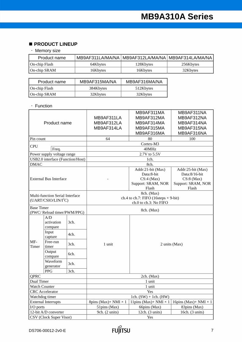
PRODUCT LINEUP Memory size
Product name MB9AF311LA/MA/NA MB9AF312LA/MA/NA MB9AF314LA/MA/NA
On-chip Flash 64Kbytes 128Kbytes 256Kbytes
On-chip SRAM 16Kbytes 16Kbytes 32Kbytes
Product name MB9AF315MA/NA MB9AF316MA/NA
On-chip Flash 384Kbytes 512Kbytes
On-chip SRAM 32Kbytes 32Kbytes
Function
Product name MB9AF311LA MB9AF312LA MB9AF314LA
MB9AF311MA MB9AF312MA MB9AF314MA MB9AF315MA MB9AF316MA
MB9AF311NA MB9AF312NA MB9AF314NA MB9AF315NA MB9AF316NA
Pin count 64 80 100 Cortex-M3
CPU Freq. 40MHz
Power supply voltage range 2.7V to 5.5V USB2.0 interface (Function/Host) 1ch. DMAC 8ch.
External Bus Interface -
Addr:21-bit (Max) Data:8-bit
CS:4 (Max) Support: SRAM, NOR
Flash
Addr:25-bit (Max) Data:8/16-bit CS:8 (Max)
Support: SRAM, NOR Flash
Multi-function Serial Interface (UART/CSIO/LIN/I2C)
8ch. (Max) ch.4 to ch.7: FIFO (16steps × 9-bit)
ch.0 to ch.3: No FIFO Base Timer (PWC/ Reload timer/PWM/PPG)
8ch. (Max)
A/D activation compare
3ch.
Input capture
4ch.
Free-run timer
3ch.
Output compare
6ch.
Waveform generator
3ch.
MF- Timer
PPG 3ch.
1 unit 2 units (Max)
QPRC 2ch. (Max) Dual Timer 1 unit Watch Counter 1 unit CRC Accelerator Yes Watchdog timer 1ch. (SW) + 1ch. (HW) External Interrupts 8pins (Max)+ NMI × 1 11pins (Max)+ NMI × 1 16pins (Max)+ NMI × 1I/O ports 51pins (Max) 66pins (Max) 83pins (Max) 12-bit A/D converter 9ch. (2 units) 12ch. (3 units) 16ch. (3 units) CSV (Clock Super Visor) Yes

8
FUJITSU SEMICONDUCTOR CONFIDENTIAL r2.1
MB9A310A Series
DS706-00012-2v0-E
Product name MB9AF311LA MB9AF312LA MB9AF314LA
MB9AF311MA MB9AF312MA MB9AF314MA MB9AF315MA MB9AF316MA
MB9AF311NA MB9AF312NA MB9AF314NA MB9AF315NA MB9AF316NA
LVD (Low-Voltage Detector) 2ch. High-speed 4MHz (± 2%) Built-in
CR Low-speed 100kHz (Typ) Debug Function SWJ-DP SWJ-DP/ETM
Note: All signals of the peripheral function in each product cannot be allocated by limiting the pins of package. It is necessary to use the port relocate function of the I/O port according to your function use.

9
FUJITSU SEMICONDUCTOR CONFIDENTIAL r2.1
MB9A310A Series
DS706-00012-2v0-E
PACKAGES
Product namePackage
MB9AF311LAMB9AF312LAMB9AF314LA
MB9AF311MA MB9AF312MA MB9AF314MA MB9AF315MA MB9AF316MA
MB9AF311NAMB9AF312NAMB9AF314NAMB9AF315NAMB9AF316NA
LQFP:FPT-64P-M24/M38 (0.5mm pitch) - -
LQFP:FPT-64P-M23/M39 (0.65mm pitch) - -
QFN:LCC-64P-M24 (0.5mm pitch) - -
LQFP:FPT-80P-M21/M37 (0.5mm pitch) - -
LQFP:FPT-100P-M20/M23 (0.5mm pitch) - -
QFP:FPT-100P-M06 (0.65mm pitch) - -
BGA:BGA-112P-M04 (0.8mm pitch) - - * : Supported * : MB9AF315NA, MB9AF316NA are planning Note: Refer to "PACKAGE DIMENSIONS" for detailed information on each package.

10
FUJITSU SEMICONDUCTOR CONFIDENTIAL r2.1
MB9A310A Series
DS706-00012-2v0-E
PIN ASSIGNMENT FPT-100P-M20/M23
(TOP VIEW)
VS
S
P81
/UD
P0
P80
/UD
M0
US
BV
CC
P60
/SIN
5_0/
TIO
A2_
2/IN
T15
_1/M
RD
Y_1
P61
/SO
T5_
0/T
IOB
2_2/
UH
CO
NX
P62
/SC
K5_
0/A
DT
G_3
/MO
EX
_1
P63
/INT
03_0
/MW
EX
_1
P0F
/NM
IX/C
RO
UT
_1
P0E
/CT
S4_
0/T
IOB
3_2/
IC13
_0/M
DQ
M1_
1
P0D
/RT
S4_
0/T
IOA
3_2/
IC12
_0/M
DQ
M0_
1
P0C
/SC
K4_
0/T
IOA
6_1/
IC11
_0/M
AL
E_1
P0B
/SO
T4_
0/T
IOB
6_1/
IC10
_0/M
CS
X0_
1
P0A
/SIN
4_0/
INT
00_2
/FR
CK
1_0/
MC
SX
1_1
P09
/TR
AC
EC
LK
/TIO
B0_
2/R
TS
4_2/
MC
SX
2_1
P08
/TR
AC
ED
3/T
IOA
0_2/
CT
S4_
2/M
CS
X3_
1
P07
/TR
AC
ED
2/A
DT
G_0
/SC
K4_
2/M
CL
KO
UT
_1
P06
/TR
AC
ED
1/T
IOB
5_2/
SO
T4_
2/IN
T01
_1/M
CS
X4_
1
P05
/TR
AC
ED
0/T
IOA
5_2/
SIN
4_2/
INT
00_1
/MC
SX
5_1
P04
/TD
O/S
WO
P03
/TM
S/S
WD
IO
P02
/TD
I/MC
SX
6_1
P01
/TC
K/S
WC
LK
P00
/TR
ST
X/M
CS
X7_
1
VC
C
100
99 98 97 96 95 94 93 92 91 90 89 88 87 86 85 84 83 82 81 80 79 78 77 76
VCC 1 75 VSS
P50/INT00_0/AIN0_2/SIN3_1/RTO10_0/MADATA00_1 2 74 P20/INT05_0/CROUT_0/AIN1_1/MAD24_1
P51/INT01_0/BIN0_2/SOT3_1/RTO11_0/MADATA01_1 3 73 P21/SIN0_0/INT06_1/BIN1_1
P52/INT02_0/ZIN0_2/SCK3_1/RTO12_0/MADATA02_1 4 72 P22/SOT0_0/TIOB7_1/ZIN1_1
P53/SIN6_0/TIOA1_2/INT07_2/RTO13_0/MADATA03_1 5 71 P23/SCK0_0/TIOA7_1/RTO00_1
P54/SOT6_0/TIOB1_2/RTO14_0/MADATA04_1 6 70 P1F/AN15/ADTG_5/FRCK0_1/MAD23_1
P55/SCK6_0/ADTG_1/RTO15_0/MADATA05_1 7 69 P1E/AN14/RTS4_1/DTTI0X_1/MAD22_1
P56/INT08_2/DTTI1X_0/MADATA06_1 8 68 P1D/AN13/CTS4_1/IC03_1/MAD21_1
P30/AIN0_0/TIOB0_1/INT03_2/MADATA07_1 9 67 P1C/AN12/SCK4_1/IC02_1/MAD20_1
P31/BIN0_0/TIOB1_1/SCK6_1/INT04_2/MADATA08_1 10 66 P1B/AN11/SOT4_1/IC01_1/MAD19_1
P32/ZIN0_0/TIOB2_1/SOT6_1/INT05_2/MADATA09_1 11 65 P1A/AN10/SIN4_1/INT05_1/IC00_1/MAD18_1
P33/INT04_0/TIOB3_1/SIN6_1/ADTG_6/MADATA10_1 12 64 P19/AN09/SCK2_2/MAD17_1
P34/FRCK0_0/TIOB4_1/MADATA11_1 13 63 P18/AN08/SOT2_2/MAD16_1
P35/IC03_0/TIOB5_1/INT08_1/MADATA12_1 14 62 AVSS
P36/IC02_0/SIN5_2/INT09_1/MADATA13_1 15 61 AVRH
P37/IC01_0/SOT5_2/INT10_1/MADATA14_1 16 60 AVCC
P38/IC00_0/SCK5_2/INT11_1/MADATA15_1 17 59 P17/AN07/SIN2_2/INT04_1/MAD15_1
P39/DTTI0X_0/ADTG_2 18 58 P16/AN06/SCK0_1/MAD14_1
P3A/RTO00_0/TIOA0_1 19 57 P15/AN05/SOT0_1/IC03_2/MAD13_1
P3B/RTO01_0/TIOA1_1 20 56 P14/AN04/SIN0_1/INT03_1/IC02_2/MAD12_1
P3C/RTO02_0/TIOA2_1 21 55 P13/AN03/SCK1_1/IC01_2/MAD11_1
P3D/RTO03_0/TIOA3_1 22 54 P12/AN02/SOT1_1/IC00_2/MAD10_1
P3E/RTO04_0/TIOA4_1 23 53 P11/AN01/SIN1_1/INT02_1/FRCK0_2/MAD09_1
P3F/RTO05_0/TIOA5_1 24 52 P10/AN00
VSS 25 51 VCC
26 27 28 29 30 31 32 33 34 35 36 37 38 39 40 41 42 43 44 45 46 47 48 49 50
VC
C
P40
/TIO
A0_
0/R
TO
10_1
/INT
12_1
P41
/TIO
A1_
0/R
TO
11_1
/INT
13_1
P42
/TIO
A2_
0/R
TO
12_1
P43
/TIO
A3_
0/R
TO
13_1
/AD
TG
_7
P44
/TIO
A4_
0/R
TO
14_1
/MA
D00
_1
P45
/TIO
A5_
0/R
TO
15_1
/MA
D01
_1 C
VS
S
VC
C
P46
/X0A
P47
/X1A
INIT
X
P48
/DT
TI1
X_1
/INT
14_1
/SIN
3_2/
MA
D02
_1
P49
/TIO
B0_
0/IC
10_1
/AIN
0_1/
SO
T3_
2/M
AD
03_1
P4A
/TIO
B1_
0/IC
11_1
/BIN
0_1/
SC
K3_
2/M
AD
04_1
P4B
/TIO
B2_
0/IC
12_1
/ZIN
0_1/
MA
D05
_1
P4C
/TIO
B3_
0/IC
13_1
/SC
K7_
1/A
IN1_
2/M
AD
06_1
P4D
/TIO
B4_
0/F
RC
K1_
1/S
OT
7_1/
BIN
1_2/
MA
D07
_1
P4E
/TIO
B5_
0/IN
T06
_2/S
IN7_
1/Z
IN1_
2/M
AD
08_1
PE
0/M
D1
MD
0
PE
2/X
0
PE
3/X
1
VS
S
LQFP - 100
<Note>
The number after the underscore ("_") in pin names such as XXX_1 and XXX_2 indicates the relocated port number. For these pins, there are multiple pins that provide the same function for the same channel. Use the extended port function register (EPFR) to select the pin.

11
FUJITSU SEMICONDUCTOR CONFIDENTIAL r2.1
MB9A310A Series
DS706-00012-2v0-E
FPT-100P-M06
(TOP VIEW)
P50
/INT
00_0
/AIN
0_2/
SIN
3_1/
RT
O10
_0/M
AD
AT
A00
_1
VC
C
VS
S
P81
/UD
P0
P80
/UD
M0
US
BV
CC
P60
/SIN
5_0/
TIO
A2_
2/IN
T15
_1/M
RD
Y_1
P61
/SO
T5_
0/T
IOB
2_2/
UH
CO
NX
P62
/SC
K5_
0/A
DT
G_3
/MO
EX
_1
P63
/INT
03_0
/MW
EX
_1
P0F
/NM
IX/C
RO
UT
_1
P0E
/CT
S4_
0/T
IOB
3_2/
IC13
_0/M
DQ
M1_
1
P0D
/RT
S4_
0/T
IOA
3_2/
IC12
_0/M
DQ
M0_
1
P0C
/SC
K4_
0/T
IOA
6_1/
IC11
_0/M
AL
E_1
P0B
/SO
T4_
0/T
IOB
6_1/
IC10
_0/M
CS
X0_
1
P0A
/SIN
4_0/
INT
00_2
/FR
CK
1_0/
MC
SX
1_1
P09
/TR
AC
EC
LK
/TIO
B0_
2/R
TS
4_2/
MC
SX
2_1
P08
/TR
AC
ED
3/T
IOA
0_2/
CT
S4_
2/M
CS
X3_
1
P07
/TR
AC
ED
2/A
DT
G_0
/SC
K4_
2/M
CL
KO
UT
_1
P06
/TR
AC
ED
1/T
IOB
5_2/
SO
T4_
2/IN
T01
_1/M
CS
X4_
1
P05
/TR
AC
ED
0/T
IOA
5_2/
SIN
4_2/
INT
00_1
/MC
SX
5_1
P04
/TD
O/S
WO
P03
/TM
S/S
WD
IO
P02
/TD
I/MC
SX
6_1
P01
/TC
K/S
WC
LK
P00
/TR
ST
X/M
CS
X7_
1
VC
C
VS
S
P20
/INT
05_0
/CR
OU
T_0
/AIN
1_1/
MA
D24
_1
P21
/SIN
0_0/
INT
06_1
/BIN
1_1
80 79 78 77 76 75 74 73 72 71 70 69 68 67 66 65 64 63 62 61 60 59 58 57 56 55 54 53 52 51
P51/INT01_0/BIN0_2/SOT3_1/RTO11_0/MADATA01_1 81 50 P22/SOT0_0/TIOB7_1/ZIN1_1
P52/INT02_0/ZIN0_2/SCK3_1/RTO12_0/MADATA02_1 82 49 P23/SCK0_0/TIOA7_1/RTO00_1
P53/SIN6_0/TIOA1_2/INT07_2/RTO13_0/MADATA03_1 83 48 P1F/AN15/ADTG_5/FRCK0_1/MAD23_1
P54/SOT6_0/TIOB1_2/RTO14_0/MADATA04_1 84 47 P1E/AN14/RTS4_1/DTTI0X_1/MAD22_1
P55/SCK6_0/ADTG_1/RTO15_0/MADATA05_1 85 46 P1D/AN13/CTS4_1/IC03_1/MAD21_1
P56/INT08_2/DTTI1X_0/MADATA06_1 86 45 P1C/AN12/SCK4_1/IC02_1/MAD20_1
P30/AIN0_0/TIOB0_1/INT03_2/MADATA07_1 87 44 P1B/AN11/SOT4_1/IC01_1/MAD19_1
P31/BIN0_0/TIOB1_1/SCK6_1/INT04_2/MADATA08_1 88 43 P1A/AN10/SIN4_1/INT05_1/IC00_1/MAD18_1
P32/ZIN0_0/TIOB2_1/SOT6_1/INT05_2/MADATA09_1 89 42 P19/AN09/SCK2_2/MAD17_1
P33/INT04_0/TIOB3_1/SIN6_1/ADTG_6/MADATA10_1 90 41 P18/AN08/SOT2_2/MAD16_1
P34/FRCK0_0/TIOB4_1/MADATA11_1 91 40 AVSS
P35/IC03_0/TIOB5_1/INT08_1/MADATA12_1 92 39 AVRH
P36/IC02_0/SIN5_2/INT09_1/MADATA13_1 93 38 AVCC
P37/IC01_0/SOT5_2/INT10_1/MADATA14_1 94 37 P17/AN07/SIN2_2/INT04_1/MAD15_1
P38/IC00_0/SCK5_2/INT11_1/MADATA15_1 95 36 P16/AN06/SCK0_1/MAD14_1
P39/DTTI0X_0/ADTG_2 96 35 P15/AN05/SOT0_1/IC03_2/MAD13_1
P3A/RTO00_0/TIOA0_1 97 34 P14/AN04/SIN0_1/INT03_1/IC02_2/MAD12_1
P3B/RTO01_0/TIOA1_1 98 33 P13/AN03/SCK1_1/IC01_2/MAD11_1
P3C/RTO02_0/TIOA2_1 99 32 P12/AN02/SOT1_1/IC00_2/MAD10_1
P3D/RTO03_0/TIOA3_1 100 31 P11/AN01/SIN1_1/INT02_1/FRCK0_2/MAD09_1
1 2 3 4 5 6 7 8 9 10 11 12 13 14 15 16 17 18 19 20 21 22 23 24 25 26 27 28 29 30
P3E
/RT
O04
_0/T
IOA
4_1
P3F
/RT
O05
_0/T
IOA
5_1
VS
S
VC
C
P40
/TIO
A0_
0/R
TO
10_1
/INT
12_1
P41
/TIO
A1_
0/R
TO
11_1
/INT
13_1
P42
/TIO
A2_
0/R
TO
12_1
P43
/TIO
A3_
0/R
TO
13_1
/AD
TG
_7
P44
/TIO
A4_
0/R
TO
14_1
/MA
D00
_1
P45
/TIO
A5_
0/R
TO
15_1
/MA
D01
_1 C
VS
S
VC
C
P46
/X0A
P47
/X1A
INIT
X
P48
/DT
TI1
X_1
/INT
14_1
/SIN
3_2/
MA
D02
_1
P49
/TIO
B0_
0/IC
10_1
/AIN
0_1/
SO
T3_
2/M
AD
03_1
P4A
/TIO
B1_
0/IC
11_1
/BIN
0_1/
SC
K3_
2/M
AD
04_1
P4B
/TIO
B2_
0/IC
12_1
/ZIN
0_1/
MA
D05
_1
P4C
/TIO
B3_
0/IC
13_1
/SC
K7_
1/A
IN1_
2/M
AD
06_1
P4D
/TIO
B4_
0/F
RC
K1_
1/S
OT
7_1/
BIN
1_2/
MA
D07
_1
P4E
/TIO
B5_
0/IN
T06
_2/S
IN7_
1/Z
IN1_
2/M
AD
08_1
PE
0/M
D1
MD
0
PE
2/X
0
PE
3/X
1
VS
S
VC
C
P10
/AN
00
QFP - 100
<Note>
The number after the underscore ("_") in pin names such as XXX_1 and XXX_2 indicates the relocated port number. For these pins, there are multiple pins that provide the same function for the same channel. Use the extended port function register (EPFR) to select the pin.

12
FUJITSU SEMICONDUCTOR CONFIDENTIAL r2.1
MB9A310A Series
DS706-00012-2v0-E
FPT-80P-M21/FPT-80P-M37
(TOP VIEW)
VS
S
P81
/UD
P0
P80
/UD
M0
US
BV
CC
P60
/SIN
5_0/
TIO
A2_
2/IN
T15
_1/M
RD
Y_1
P61
/SO
T5_
0/T
IOB
2_2/
UH
CO
NX
P62
/SC
K5_
0/A
DT
G_3
/MO
EX
_1
P63
/INT
03_0
/MW
EX
_1
P0F
/NM
IX/C
RO
UT
_1
P0E
/CT
S4_
0/T
IOB
3_2/
IC13
_0/M
DQ
M1_
1
P0D
/RT
S4_
0/T
IOA
3_2/
IC12
_0/M
DQ
M0_
1
P0C
/SC
K4_
0/T
IOA
6_1/
IC11
_0/M
AL
E_1
P0B
/SO
T4_
0/T
IOB
6_1/
IC10
_0/M
CS
X0_
1
P0A
/SIN
4_0/
INT
00_2
/FR
CK
1_0/
MC
SX
1_1
P07
/AD
TG
_0/M
CL
KO
UT
_1
P04
/TD
O/S
WO
P03
/TM
S/S
WD
IO
P02
/TD
I/MC
SX
6_1
P01
/TC
K/S
WC
LK
P00
/TR
ST
X/M
CS
X7_
1
80 79 78 77 76 75 74 73 72 71 70 69 68 67 66 65 64 63 62 61
VCC 1 60 P20/INT05_0/CROUT_0/AIN1_1/MAD24_1
P50/INT00_0/AIN0_2/SIN3_1/RTO10_0/MADATA00_1 2 59 P21/SIN0_0/INT06_1/BIN1_1
P51/INT01_0/BIN0_2/SOT3_1/RTO11_0/MADATA01_1 3 58 P22/SOT0_0/TIOB7_1/ZIN1_1
P52/INT02_0/ZIN0_2/SCK3_1/RTO12_0/MADATA02_1 4 57 P23/SCK0_0/TIOA7_1
P53/SIN6_0/TIOA1_2/INT07_2/RTO13_0/MADATA03_1 5 56 P1B/AN11/SOT4_1/IC01_1/MAD19_1
P54/SOT6_0/TIOB1_2/RTO14_0/MADATA04_1 6 55 P1A/AN10/SIN4_1/INT05_1/IC00_1/MAD18_1
P55/SCK6_0/ADTG_1/RTO15_0/MADATA05_1 7 54 P19/AN09/SCK2_2/MAD17_1
P56/INT08_2/DTTI1X_0/MADATA06_1 8 53 P18/AN08/SOT2_2/MAD16_1
P30/AIN0_0/TIOB0_1/INT03_2/MADATA07_1 9 52 AVSS
P31/BIN0_0/TIOB1_1/SCK6_1/INT04_2/MADATA08_1 10 51 AVRH
P32/ZIN0_0/TIOB2_1/SOT6_1/INT05_2/MADATA09_1 11 50 AVCC
P33/INT04_0/TIOB3_1/SIN6_1/ADTG_6/MADATA10_1 12 49 P17/AN07/SIN2_2/INT04_1/MAD15_1
P39/DTTI0X_0/ADTG_2 13 48 P16/AN06/SCK0_1/MAD14_1
P3A/RTO00_0/TIOA0_1 14 47 P15/AN05/SOT0_1/IC03_2/MAD13_1
P3B/RTO01_0/TIOA1_1 15 46 P14/AN04/SIN0_1/INT03_1/IC02_2/MAD12_1
P3C/RTO02_0/TIOA2_1 16 45 P13/AN03/SCK1_1/IC01_2/MAD11_1
P3D/RTO03_0/TIOA3_1 17 44 P12/AN02/SOT1_1/IC00_2/MAD10_1
P3E/RTO04_0/TIOA4_1 18 43 P11/AN01/SIN1_1/INT02_1/FRCK0_2/MAD09_1
P3F/RTO05_0/TIOA5_1 19 42 P10/AN00
VSS 20 41 VCC
21 22 23 24 25 26 27 28 29 30 31 32 33 34 35 36 37 38 39 40
P44
/TIO
A4_
0/M
AD
00_1
P45
/TIO
A5_
0/M
AD
01_1 C
VS
S
VC
C
P46
/X0A
P47
/X1A
INIT
X
P48
/DT
TI1
X_1
/INT
14_1
/SIN
3_2/
MA
D02
_1
P49
/TIO
B0_
0/IC
10_1
/AIN
0_1/
SO
T3_
2/M
AD
03_1
P4A
/TIO
B1_
0/IC
11_1
/BIN
0_1/
SC
K3_
2/M
AD
04_1
P4B
/TIO
B2_
0/IC
12_1
/ZIN
0_1/
MA
D05
_1
P4C
/TIO
B3_
0/IC
13_1
/SC
K7_
1/A
IN1_
2/M
AD
06_1
P4D
/TIO
B4_
0/F
RC
K1_
1/S
OT
7_1/
BIN
1_2/
MA
D07
_1
P4E
/TIO
B5_
0/IN
T06
_2/S
IN7_
1/Z
IN1_
2/M
AD
08_1
PE
0/M
D1
MD
0
PE
2/X
0
PE
3/X
1
VS
S
LQFP - 80
<Note>
The number after the underscore ("_") in pin names such as XXX_1 and XXX_2 indicates the relocated port number. For these pins, there are multiple pins that provide the same function for the same channel. Use the extended port function register (EPFR) to select the pin.

13
FUJITSU SEMICONDUCTOR CONFIDENTIAL r2.1
MB9A310A Series
DS706-00012-2v0-E
FPT-64P-M23/M24/M38/M39
(TOP VIEW)
VS
S
P81
/UD
P0
P80
/UD
M0
US
BV
CC
P60
/SIN
5_0/
TIO
A2_
2/IN
T15
_1
P61
/SO
T5_
0/T
IOB
2_2/
UH
CO
NX
P62
/SC
K5_
0/A
DT
G_3
P0F
/NM
IX/C
RO
UT
_1
P0C
/SC
K4_
0/T
IOA
6_1
P0B
/SO
T4_
0/T
IOB
6_1
P0A
/SIN
4_0/
INT
00_2
P04
/TD
O/S
WO
P03
/TM
S/S
WD
IO
P02
/TD
I
P01
/TC
K/S
WC
LK
P00
/TR
ST
X
64 63 62 61 60 59 58 57 56 55 54 53 52 51 50 49
VCC 1 48 P21/SIN0_0/INT06_1
P50/INT00_0/AIN0_2/SIN3_1 2 47 P22/SOT0_0/TIOB7_1
P51/INT01_0/BIN0_2/SOT3_1 3 46 P23/SCK0_0/TIOA7_1
P52/INT02_0/ZIN0_2/SCK3_1 4 45 P19/AN09/SCK2_2
P30/AIN0_0/TIOB0_1/INT03_2 5 44 P18/AN08/SOT2_2
P31/BIN0_0/TIOB1_1/SCK6_1/INT04_2 6 43 AVSS
P32/ZIN0_0/TIOB2_1/SOT6_1/INT05_2 7 42 AVRH
P33/INT04_0/TIOB3_1/SIN6_1/ADTG_6 8 41 AVCC
P39/DTTI0X_0/ADTG_2 9 40 P17/AN07/SIN2_2/INT04_1
P3A/RTO00_0/TIOA0_1 10 39 P15/AN05/IC03_2
P3B/RTO01_0/TIOA1_1 11 38 P14/AN04/INT03_1/IC02_2
P3C/RTO02_0/TIOA2_1 12 37 P13/AN03/SCK1_1/IC01_2
P3D/RTO03_0/TIOA3_1 13 36 P12/AN02/SOT1_1/IC00_2
P3E/RTO04_0/TIOA4_1 14 35 P11/AN01/SIN1_1/INT02_1/FRCK0_2
P3F/RTO05_0/TIOA5_1 15 34 P10/AN00
VSS 16 33 VCC
17 18 19 20 21 22 23 24 25 26 27 28 29 30 31 32
C
VC
C
P46
/X0A
P47
/X1A
INIT
X
P49
/TIO
B0_
0/A
IN0_
1
P4A
/TIO
B1_
0/B
IN0_
1
P4B
/TIO
B2_
0/Z
IN0_
1
P4C
/TIO
B3_
0/S
CK
7_1/
AIN
1_2
P4D
/TIO
B4_
0/S
OT
7_1/
BIN
1_2
P4E
/TIO
B5_
0/IN
T06
_2/S
IN7_
1/Z
IN1_
2
PE
0/M
D1
MD
0
PE
2/X
0
PE
3/X
1
VS
S
LQFP - 64
<Note>
The number after the underscore ("_") in pin names such as XXX_1 and XXX_2 indicates the relocated port number. For these pins, there are multiple pins that provide the same function for the same channel. Use the extended port function register (EPFR) to select the pin.
14
FUJITSU SEMICONDUCTOR CONFIDENTIAL r2.1
MB9A310A Series
DS706-00012-2v0-E
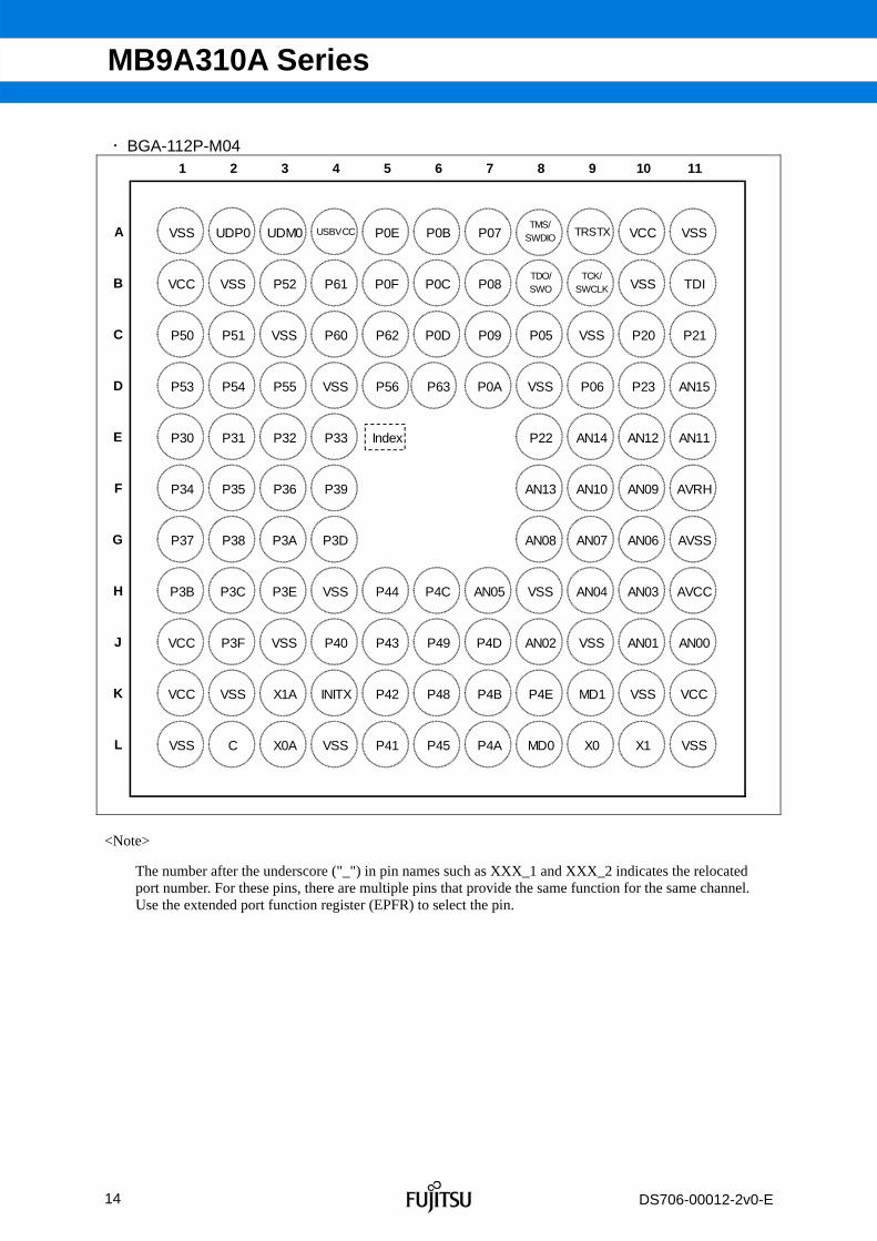
BGA-112P-M04
P4A MD0 X0 X1 VSS
MD1 VSS VCC
L VSS C X0A VSS P41 P45
J VCC P3F VSS P40 AN00
K VCC VSS X1A INITX P42 P48 P4B P4E
P43 P49 P4D AN02 VSS AN01
AN07 AN06 AVSS
H P3B P3C P3E VSS P44 P4C
G P37 P38 P3A P3D AN08
AN05 VSS AN04 AN03 AVCC
AN11
F P34 P35 P36 P39 AN13 AN10 AN09 AVRH
E P30 P31 P32 P33 Index P22 AN14 AN12
VSS P20 P21
D P53 P54 P55 VSS AN15P56 P63 P0A VSS P06 P23
C P50 P51 VSS P60 P62 P0D P09 P05
B VCC VSS P52 P61 P0F P0C P08TDO/SWO
P0B P07TMS/
SWDIO TRSTX VCC VSS
TCK/SWCLK VSS TDI
9 10 11
A VSS UDP0 UDM0 USBVCC P0E
1 2 3 4 5 6 7 8
<Note>
The number after the underscore ("_") in pin names such as XXX_1 and XXX_2 indicates the relocated port number. For these pins, there are multiple pins that provide the same function for the same channel. Use the extended port function register (EPFR) to select the pin.

15
FUJITSU SEMICONDUCTOR CONFIDENTIAL r2.1
MB9A310A Series
DS706-00012-2v0-E
LCC-64P-M24
(TOP VIEW)
VS
S
P81
/UD
P0
P80
/UD
M0
US
BV
CC
P60
/SIN
5_0/
TIO
A2_
2/IN
T15
_1
P61
/SO
T5_
0/T
IOB
2_2/
UH
CO
NX
P62
/SC
K5_
0/A
DT
G_3
P0F
/NM
IX/C
RO
UT
_1
P0C
/SC
K4_
0/T
IOA
6_1
P0B
/SO
T4_
0/T
IOB
6_1
P0A
/SIN
4_0/
INT
00_2
P04
/TD
O/S
WO
P03
/TM
S/S
WD
IO
P02
/TD
I
P01
/TC
K/S
WC
LK
P00
/TR
ST
X
64 63 62 61 60 59 58 57 56 55 54 53 52 51 50 49
VCC 1 48 P21/SIN0_0/INT06_1
P50/INT00_0/AIN0_2/SIN3_1 2 47 P22/SOT0_0/TIOB7_1
P51/INT01_0/BIN0_2/SOT3_1 3 46 P23/SCK0_0/TIOA7_1
P52/INT02_0/ZIN0_2/SCK3_1 4 45 P19/AN09/SCK2_2
P30/AIN0_0/TIOB0_1/INT03_2 5 44 P18/AN08/SOT2_2
P31/BIN0_0/TIOB1_1/SCK6_1/INT04_2 6 43 AVSS
P32/ZIN0_0/TIOB2_1/SOT6_1/INT05_2 7 42 AVRH
P33/INT04_0/TIOB3_1/SIN6_1/ADTG_6 8 41 AVCC
P39/DTTI0X_0/ADTG_2 9 40 P17/AN07/SIN2_2/INT04_1
P3A/RTO00_0/TIOA0_1 10 39 P15/AN05/IC03_2
P3B/RTO01_0/TIOA1_1 11 38 P14/AN04/INT03_1/IC02_2
P3C/RTO02_0/TIOA2_1 12 37 P13/AN03/SCK1_1/IC01_2
P3D/RTO03_0/TIOA3_1 13 36 P12/AN02/SOT1_1/IC00_2
P3E/RTO04_0/TIOA4_1 14 35 P11/AN01/SIN1_1/INT02_1/FRCK0_2
P3F/RTO05_0/TIOA5_1 15 34 P10/AN00
VSS 16 33 VCC
17 18 19 20 21 22 23 24 25 26 27 28 29 30 31 32
C
VC
C
P46
/X0A
P47
/X1A
INIT
X
P49
/TIO
B0_
0/A
IN0_
1
P4A
/TIO
B1_
0/B
IN0_
1
P4B
/TIO
B2_
0/Z
IN0_
1
P4C
/TIO
B3_
0/S
CK
7_1/
AIN
1_2
P4D
/TIO
B4_
0/S
OT
7_1/
BIN
1_2
P4E
/TIO
B5_
0/IN
T06
_2/S
IN7_
1/Z
IN1_
2
PE
0/M
D1
MD
0
PE
2/X
0
PE
3/X
1
VS
S
QFN - 64
<Note>
The number after the underscore ("_") in pin names such as XXX_1 and XXX_2 indicates the relocated port number. For these pins, there are multiple pins that provide the same function for the same channel. Use the extended port function register (EPFR) to select the pin.

16
FUJITSU SEMICONDUCTOR CONFIDENTIAL r2.1
MB9A310A Series
DS706-00012-2v0-E
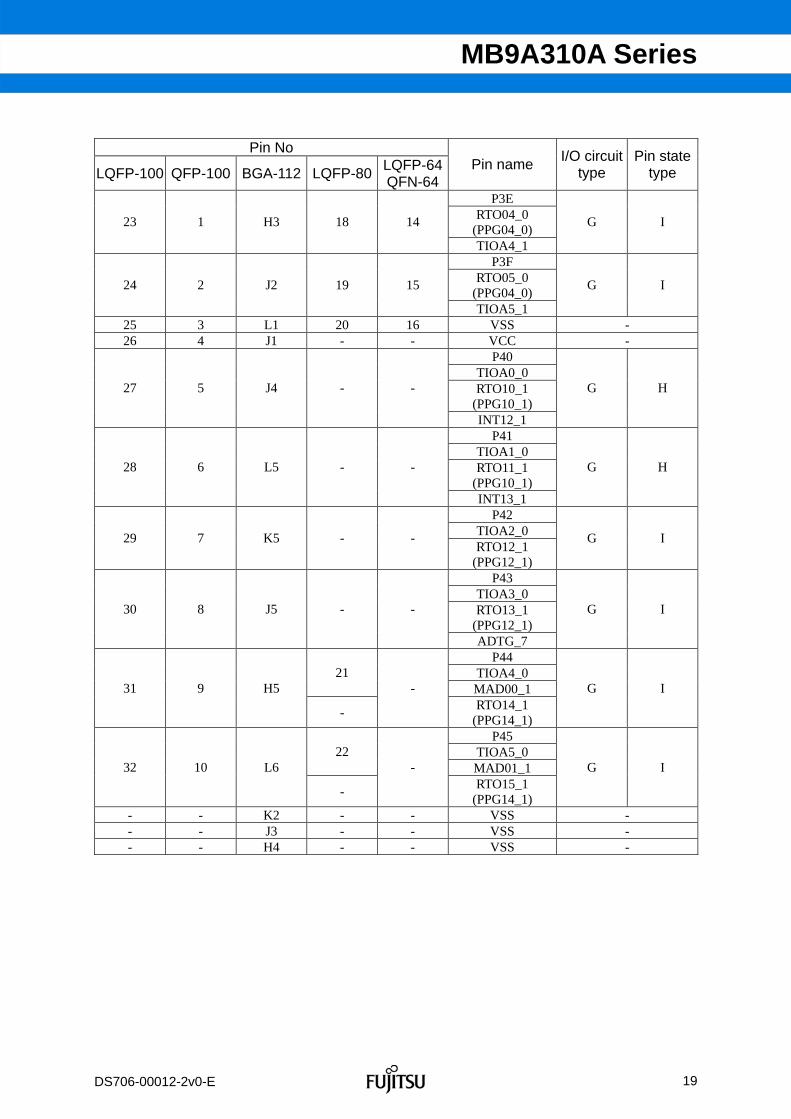
PIN DESCRIPTION The number after the underscore ("_") in pin names such as XXX_1 and XXX_2 indicates the relocated port number. For these pins, there are multiple pins that provide the same function for the same channel. Use the extended port function register (EPFR) to select the pin.
Pin No
LQFP-100 QFP-100 BGA-112 LQFP-80LQFP-64QFN-64
Pin name I/O circuit
type Pin state
type
1 79 B1 1 1 VCC - P50
INT00_0 AIN0_2
2
SIN3_1 RTO10_0
(PPG10_0)
2 80 C1 2
- MADATA00_1
E H
P51 INT01_0 BIN0_2 3 SOT3_1
(SDA3_1) RTO11_0
(PPG10_0)
3 81 C2 3
- MADATA01_1
E H
P52 INT02_0 ZIN0_2 4 SCK3_1
(SCL3_1) RTO12_0
(PPG12_0)
4 82 B3 4
- MADATA02_1
E H
P53 SIN6_0
TIOA1_2 INT07_2 RTO13_0
(PPG12_0)
5 83 D1 5 -
MADATA03_1
E H
P54 SOT6_0
(SDA6_0) TIOB1_2 RTO14_0
(PPG14_0)
6 84 D2 6 -
MADATA04_1
E I

17
FUJITSU SEMICONDUCTOR CONFIDENTIAL r2.1
MB9A310A Series
DS706-00012-2v0-E
Pin No
LQFP-100 QFP-100 BGA-112 LQFP-80LQFP-64QFN-64
Pin name I/O circuit
type Pin state
type
P55 SCK6_0
(SCL6_0) ADTG_1 RTO15_0
(PPG14_0)
7 85 D3 7 -
MADATA05_1
E I
P56 INT08_2
DTTI1X_0 8 86 D5 8 -
MADATA06_1
E H
P30 AIN0_0
TIOB0_1 5
INT03_2 9 87 E1 9
- MADATA07_1
E H
P31 BIN0_0
TIOB1_1 SCK6_1
(SCL6_1)
6
INT04_2
10 88 E2 10
- MADATA08_1
E H
P32 ZIN0_0
TIOB2_1 SOT6_1
(SDA6_1)
7
INT05_2
11 89 E3 11
- MADATA09_1
E H
P33 INT04_0 TIOB3_1 SIN6_1
8
ADTG_6
12 90 E4 12
- MADATA10_1
E H
P34 FRCK0_0 TIOB4_1
13 91 F1 - -
MADATA11_1
E I

18
FUJITSU SEMICONDUCTOR CONFIDENTIAL r2.1
MB9A310A Series
DS706-00012-2v0-E
Pin No
LQFP-100 QFP-100 BGA-112 LQFP-80LQFP-64QFN-64
Pin name I/O circuit
type Pin state
type
P35 IC03_0
TIOB5_1 INT08_1
14 92 F2 - -
MADATA12_1
E H
P36 IC02_0 SIN5_2
INT09_1 15 93 F3 - -
MADATA13_1
E H
P37 IC01_0 SOT5_2
(SDA5_2) INT10_1
16 94 G1 - -
MADATA14_1
E H
P38 IC00_0 SCK5_2
(SCL5_2) INT11_1
17 95 G2 - -
MADATA15_1
E H
P39 DTTI0X_0 18 96 F4 13 9 ADTG_2
E I
P3A RTO00_0
(PPG00_0) 19 97 G3 14 10
TIOA0_1
G I
P3B RTO01_0
(PPG00_0) 20 98 H1 15 11
TIOA1_1
G I
P3C RTO02_0
(PPG02_0) 21 99 H2 16 12
TIOA2_1
G I
P3D RTO03_0
(PPG02_0) 22 100 G4 17 13
TIOA3_1
G I
- - B2 - - VSS -
19
FUJITSU SEMICONDUCTOR CONFIDENTIAL r2.1
MB9A310A Series
DS706-00012-2v0-E
Pin No
LQFP-100 QFP-100 BGA-112 LQFP-80LQFP-64QFN-64
Pin name I/O circuit
type Pin state
type
P3E RTO04_0
(PPG04_0) 23 1 H3 18 14
TIOA4_1
G I
P3F RTO05_0
(PPG04_0) 24 2 J2 19 15
TIOA5_1
G I
25 3 L1 20 16 VSS - 26 4 J1 - - VCC -
P40 TIOA0_0 RTO10_1
(PPG10_1) 27 5 J4 - -
INT12_1
G H
P41 TIOA1_0 RTO11_1
(PPG10_1) 28 6 L5 - -
INT13_1
G H
P42 TIOA2_0 29 7 K5 - - RTO12_1
(PPG12_1)
G I
P43 TIOA3_0 RTO13_1
(PPG12_1) 30 8 J5 - -
ADTG_7
G I
P44 TIOA4_0 21 MAD00_1 31 9 H5
-
- RTO14_1
(PPG14_1)
G I
P45 TIOA5_0 22 MAD01_1 32 10 L6
-
- RTO15_1
(PPG14_1)
G I
- - K2 - - VSS - - - J3 - - VSS - - - H4 - - VSS -

20
FUJITSU SEMICONDUCTOR CONFIDENTIAL r2.1
MB9A310A Series
DS706-00012-2v0-E
Pin No
LQFP-100 QFP-100 BGA-112 LQFP-80LQFP-64QFN-64
Pin name I/O circuit
type Pin state
type
33 11 L2 23 17 C - 34 12 L4 24 - VSS - 35 13 K1 25 18 VCC -
P46 36 14 L3 26 19
X0A D M
P47 37 15 K3 27 20
X1A D N
38 16 K4 28 21 INITX B C P48
DTTI1X_1 INT14_1 SIN3_2
39 17 K6 29 -
MAD02_1
E H
P49 TIOB0_0 22 AIN0_1 IC10_1 SOT3_2
(SDA3_2)
40 18 J6 30
-
MAD03_1
E I
P4A TIOB1_0 23 BIN0_1 IC11_1 SCK3_2
(SCL3_2)
41 19 L7 31
-
MAD04_1
E I
P4B TIOB2_0 24 ZIN0_1 IC12_1
42 20 K7 32
- MAD05_1
E I
P4C TIOB3_0 SCK7_1
(SCL7_1) 25
AIN1_2 IC13_1
43 21 H6 33
- MAD06_1
E / I* I

21
FUJITSU SEMICONDUCTOR CONFIDENTIAL r2.1
MB9A310A Series
DS706-00012-2v0-E
Pin No
LQFP-100 QFP-100 BGA-112 LQFP-80LQFP-64QFN-64
Pin name I/O circuit
type Pin state
type
P4D TIOB4_0 SOT7_1
(SDA7_1) 26
BIN1_2 FRCK1_1
44 22 J7 34
- MAD07_1
E / I* I
P4E TIOB5_0 INT06_2 SIN7_1
27
ZIN1_2
45 23 K8 35
- MAD08_1
E / I* I
MD1 46 24 K9 36 28
PE0 C P
47 25 L8 37 29 MD0 J D X0
48 26 L9 38 30 PE2
A A
X1 49 27 L10 39 31
PE3 A B
50 28 L11 40 32 VSS - 51 29 K11 41 33 VCC -
P10 52 30 J11 42 34
AN00 F K
P11 AN01
SIN1_1 INT02_1
35
FRCK0_2
53 31 J10 43
- MAD09_1
F L
P12 AN02
SOT1_1 (SDA1_1)
36
IC00_2
54 32 J8 44
- MAD10_1
F K
- - K10 - - VSS - - - J9 - - VSS -
22
FUJITSU SEMICONDUCTOR CONFIDENTIAL r2.1
MB9A310A Series
DS706-00012-2v0-E
Pin No
LQFP-100 QFP-100 BGA-112 LQFP-80LQFP-64QFN-64
Pin name I/O circuit
type Pin state
type
P13 AN03
SCK1_1 (SCL1_1)
37
IC01_2
55 33 H10 45
- MAD11_1
F K
P14 AN04
INT03_1 38
IC02_2 SIN0_1
56 34 H9 46
- MAD12_1
F L
P15 AN05 39
IC03_2 SOT0_1
(SDA0_1)
57 35 H7 47
- MAD13_1
F K
P16 AN06
SCK0_1 (SCL0_1)
58 36 G10 48 -
MAD14_1
F K
P17 AN07
SIN2_2 40
INT04_1 59 37 G9 49
- MAD15_1
F L
60 38 H11 50 41 AVCC - 61 39 F11 51 42 AVRH - 62 40 G11 52 43 AVSS -
P18 AN08 44
SOT2_2 (SDA2_2)
63 41 G8 53
- MAD16_1
F K
P19 AN09 45
SCK2_2 (SCL2_2)
64 42 F10 54
- MAD17_1
F K
- - H8 - - VSS -

23
FUJITSU SEMICONDUCTOR CONFIDENTIAL r2.1
MB9A310A Series
DS706-00012-2v0-E
Pin No
LQFP-100 QFP-100 BGA-112 LQFP-80LQFP-64QFN-64
Pin name I/O circuit
type Pin state
type
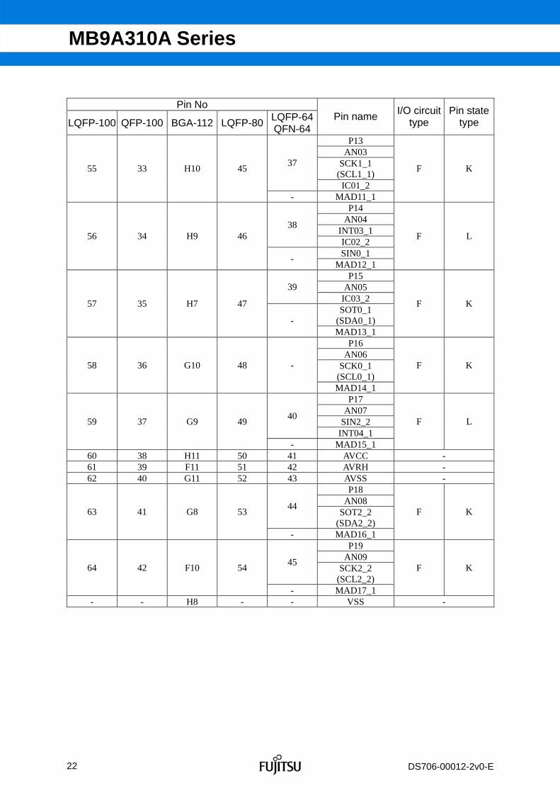
P1A AN10
SIN4_1 INT05_1 IC00_1
65 43 F9 55 -
MAD18_1
F L
P1B AN11
SOT4_1 (SDA4_1)
IC01_1
66 44 E11 56 -
MAD19_1
F K
P1C AN12
SCK4_1 (SCL4_1)
IC02_1
67 45 E10 - -
MAD20_1
F K
P1D AN13
CTS4_1 IC03_1
68 46 F8 - -
MAD21_1
F K
P1E AN14
RTS4_1 DTTI0X_1
69 47 E9 - -
MAD22_1
F K
P1F AN15
ADTG_5 FRCK0_1
70 48 D11 - -
MAD23_1
F K
- - B10 - - VSS - - - C9 - - VSS -

24
FUJITSU SEMICONDUCTOR CONFIDENTIAL r2.1
MB9A310A Series
DS706-00012-2v0-E
Pin No
LQFP-100 QFP-100 BGA-112 LQFP-80LQFP-64QFN-64
Pin name I/O circuit
type Pin state
type
P23 SCK0_0
(SCL0_0) 57 46
TIOA7_1 71 49 D10
- - RTO00_1
(PPG00_1)
E I
P22 SOT0_0
(SDA0_0) 47
TIOB7_1 72 50 E8 58
- ZIN1_1
E I
P21 SIN0_0 48
INT06_1 73 51 C11 59
- BIN1_1
E H
P20 INT05_0
CROUT_0 AIN1_1
74 52 C10 60 -
MAD24_1
E H
75 53 A11 - - VSS - 76 54 A10 - - VCC -
P00 49
TRSTX 77 55 A9 61 - MCSX7_1
E E
P01 TCK 78 56 B9 62 50
SWCLK E E
P02 51
TDI 79 57 B11 63 - MCSX6_1
E E
P03 TMS 80 58 A8 64 52
SWDIO E E
P04 TDO 81 59 B8 65 53 SWO
E E
P05 TRACED0 TIOA5_2 SIN4_2
INT00_1
82 60 C8 - -
MCSX5_1
E F
- - D8 - - VSS -

25
FUJITSU SEMICONDUCTOR CONFIDENTIAL r2.1
MB9A310A Series
DS706-00012-2v0-E
Pin No
LQFP-100 QFP-100 BGA-112 LQFP-80LQFP-64QFN-64
Pin name I/O circuit
type Pin state
type
P06 TRACED1 TIOB5_2 SOT4_2
(SDA4_2) INT01_1
83 61 D9 - -
MCSX4_1
E F
P07 ADTG_0 66
MCLKOUT_1 TRACED2
84 62 A7
-
-
SCK4_2 (SCL4_2)
E G
P08 TRACED3 TIOA0_2 CTS4_2
85 63 B7 - -
MCSX3_1
E G
P09 TRACECLK
TIOB0_2 RTS4_2
86 64 C7 - -
MCSX2_1
E G
P0A SIN4_0 54
INT00_2 FRCK1_0
87 65 D7 67
- MCSX1_1
E / I* H
P0B SOT4_0
(SDA4_0) 55
TIOB6_1 IC10_0
88 66 A6 68
- MCSX0_1
E / I* I
P0C SCK4_0
(SCL4_0) 56
TIOA6_1 IC11_0
89 67 B6 69
- MALE_1
E / I* I
- - D4 - - VSS - - - C3 - - VSS -

26
FUJITSU SEMICONDUCTOR CONFIDENTIAL r2.1
MB9A310A Series
DS706-00012-2v0-E
Pin No
LQFP-100 QFP-100 BGA-112 LQFP-80LQFP-64QFN-64
Pin name I/O circuit
type Pin state
type
P0D RTS4_0
TIOA3_2 IC12_0
90 68 C6 70 -
MDQM0_1
E I
P0E CTS4_0 TIOB3_2 IC13_0
91 69 A5 71 -
MDQM1_1
E I
P0F NMIX 92 70 B5 72 57
CROUT_1 E J
P63 INT03_0 93 71 D6 73 - MWEX_1
E H
P62 SCK5_0
(SCL5_0) 58
ADTG_3 94 72 C5 74
- MOEX_1
E I
P61 SOT5_0
(SDA5_0) TIOB2_2
95 73 B4 75 59
UHCONX
E I
P60 SIN5_0
TIOA2_2 60
INT15_1 96 74 C4 76
- MRDY_1
E / I* H
97 75 A4 77 61 USBVCC - P80
98 76 A3 78 62 UDM0
H O
P81 99 77 A2 79 63
UDP0 H O
100 78 A1 80 64 VSS - *: 5V tolerant I/O on MB9AF315MA/NA, MB9AF316MA/NA.

27
FUJITSU SEMICONDUCTOR CONFIDENTIAL r2.1
MB9A310A Series
DS706-00012-2v0-E
SIGNAL DESCRIPTION The number after the underscore ("_") in pin names such as XXX_1 and XXX_2 indicates the relocated port number. For these pins, there are multiple pins that provide the same function for the same channel. Use the extended port function register (EPFR) to select the pin.
Pin No
Module Pin name Function LQFP-
100QFP-100
BGA- 112
LQFP- 80
LQFP-64
QFN-64
ADTG_0 84 62 A7 66 - ADTG_1 7 85 D3 7 - ADTG_2 18 96 F4 13 9 ADTG_3 94 72 C5 74 58 ADTG_4 - - - - - ADTG_5 70 48 D11 - - ADTG_6 12 90 E4 12 8 ADTG_7 30 8 J5 - - ADTG_8
A/D converter external trigger input pin
- - - - - AN00 52 30 J11 42 34 AN01 53 31 J10 43 35 AN02 54 32 J8 44 36 AN03 55 33 H10 45 37 AN04 56 34 H9 46 38 AN05 57 35 H7 47 39 AN06 58 36 G10 48 - AN07 59 37 G9 49 40 AN08 63 41 G8 53 44 AN09 64 42 F10 54 45 AN10 65 43 F9 55 - AN11 66 44 E11 56 - AN12 67 45 E10 - - AN13 68 46 F8 - - AN14 69 47 E9 - -
ADC
AN15
A/D converter analog input pin ANxx describes ADC ch.xx.
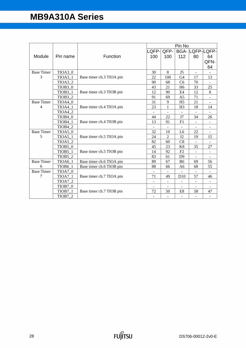
70 48 D11 - - TIOA0_0 27 5 J4 - - TIOA0_1 19 97 G3 14 10 TIOA0_2
Base timer ch.0 TIOA pin 85 63 B7 - -
TIOB0_0 40 18 J6 30 22 TIOB0_1 9 87 E1 9 5
Base Timer 0
TIOB0_2 Base timer ch.0 TIOB pin
86 64 C7 - - TIOA1_0 28 6 L5 - - TIOA1_1 20 98 H1 15 11 TIOA1_2
Base timer ch.1 TIOA pin 5 83 D1 5 -
TIOB1_0 41 19 L7 31 23 TIOB1_1 10 88 E2 10 6
Base Timer 1
TIOB1_2 Base timer ch.1 TIOB pin
6 84 D2 6 - TIOA2_0 29 7 K5 - - TIOA2_1 21 99 H2 16 12 TIOA2_2
Base timer ch.2 TIOA pin 96 74 C4 76 60
TIOB2_0 42 20 K7 32 24 TIOB2_1 11 89 E3 11 7
Base Timer 2
TIOB2_2 Base timer ch.2 TIOB pin
95 73 B4 75 59
28
FUJITSU SEMICONDUCTOR CONFIDENTIAL r2.1
MB9A310A Series
DS706-00012-2v0-E
Pin No
Module Pin name Function LQFP-
100QFP-100
BGA- 112
LQFP- 80
LQFP-64
QFN-64
TIOA3_0 30 8 J5 - - TIOA3_1 22 100 G4 17 13 TIOA3_2
Base timer ch.3 TIOA pin 90 68 C6 70 -
TIOB3_0 43 21 H6 33 25 TIOB3_1 12 90 E4 12 8
Base Timer 3
TIOB3_2 Base timer ch.3 TIOB pin
91 69 A5 71 - TIOA4_0 31 9 H5 21 - TIOA4_1 23 1 H3 18 14 TIOA4_2
Base timer ch.4 TIOA pin - - - - -
TIOB4_0 44 22 J7 34 26 TIOB4_1 13 91 F1 - -
Base Timer 4
TIOB4_2 Base timer ch.4 TIOB pin
- - - - - TIOA5_0 32 10 L6 22 - TIOA5_1 24 2 J2 19 15 TIOA5_2
Base timer ch.5 TIOA pin 82 60 C8 - -
TIOB5_0 45 23 K8 35 27 TIOB5_1 14 92 F2 - -
Base Timer 5
TIOB5_2 Base timer ch.5 TIOB pin
83 61 D9 - - TIOA6_1 Base timer ch.6 TIOA pin 89 67 B6 69 56 Base Timer
6 TIOB6_1 Base timer ch.6 TIOB pin 88 66 A6 68 55 TIOA7_0 - - - - - TIOA7_1 71 49 D10 57 46 TIOA7_2
Base timer ch.7 TIOA pin - - - - -
TIOB7_0 - - - - - TIOB7_1 72 50 E8 58 47
Base Timer 7
TIOB7_2 Base timer ch.7 TIOB pin
- - - - -

29
FUJITSU SEMICONDUCTOR CONFIDENTIAL r2.1
MB9A310A Series
DS706-00012-2v0-E
Pin No
Module Pin name Function LQFP-
100QFP-100
BGA- 112
LQFP- 80
LQFP-64
QFN-64
SWCLK Serial wire debug interface clock input 78 56 B9 62 50
SWDIO Serial wire debug interface data input / output
80 58 A8 64 52
SWO Serial wire viewer output 81 59 B8 65 53 TCK J-TAG test clock input 78 56 B9 62 50 TDI J-TAG test data input 79 57 B11 63 51 TDO J-TAG debug data output 81 59 B8 65 53 TMS J-TAG test mode state input/output 80 58 A8 64 52
TRACECLK Trace CLK output of ETM 86 64 C7 - - TRACED0 82 60 C8 - - TRACED1 83 61 D9 - - TRACED2 84 62 A7 - - TRACED3
Trace data output of ETM
85 63 B7 - -
Debugger
TRSTX J-TAG test reset Input 77 55 A9 61 49 MAD00_1 31 9 H5 21 - MAD01_1 32 10 L6 22 - MAD02_1 39 17 K6 29 - MAD03_1 40 18 J6 30 - MAD04_1 41 19 L7 31 - MAD05_1 42 20 K7 32 - MAD06_1 43 21 H6 33 - MAD07_1 44 22 J7 34 - MAD08_1 45 23 K8 35 - MAD09_1 53 31 J10 43 - MAD10_1 54 32 J8 44 - MAD11_1 55 33 H10 45 - MAD12_1 56 34 H9 46 - MAD13_1 57 35 H7 47 - MAD14_1 58 36 G10 48 - MAD15_1 59 37 G9 49 - MAD16_1 63 41 G8 53 - MAD17_1 64 42 F10 54 - MAD18_1 65 43 F9 55 - MAD19_1 66 44 E11 56 - MAD20_1 67 45 E10 - - MAD21_1 68 46 F8 - - MAD22_1 69 47 E9 - - MAD23_1 70 48 D11 - -
External Bus
MAD24_1
External bus interface address bus
74 52 C10 60 -

30
FUJITSU SEMICONDUCTOR CONFIDENTIAL r2.1
MB9A310A Series
DS706-00012-2v0-E
Pin No
Module Pin name Function LQFP-
100QFP-100
BGA- 112
LQFP- 80
LQFP-64
QFN-64
MCSX0_1 88 66 A6 68 - MCSX1_1 87 65 D7 67 - MCSX2_1 86 64 C7 - - MCSX3_1 85 63 B7 - - MCSX4_1 83 61 D9 - - MCSX5_1 82 60 C8 - - MCSX6_1 79 57 B11 63 - MCSX7_1
External bus interface chip select output pin
77 55 A9 61 - MDQM0_1 90 68 C6 70 - MDQM1_1
External bus interface byte mask signal output 91 69 A5 71 -
MOEX_1 External bus interface read enable signal for SRAM
94 72 C5 74 -
MWEX_1External bus interface write enable signal for SRAM
93 71 D6 73 -
MADATA00_1 2 80 C1 2 - MADATA01_1 3 81 C2 3 - MADATA02_1 4 82 B3 4 - MADATA03_1 5 83 D1 5 - MADATA04_1 6 84 D2 6 - MADATA05_1 7 85 D3 7 - MADATA06_1 8 86 D5 8 - MADATA07_1 9 87 E1 9 - MADATA08_1 10 88 E2 10 - MADATA09_1 11 89 E3 11 - MADATA10_1 12 90 E4 12 - MADATA11_1 13 91 F1 - - MADATA12_1 14 92 F2 - - MADATA13_1 15 93 F3 - - MADATA14_1 16 94 G1 - - MADATA15_1
External bus interface data bus
17 95 G2 - -
MALE_1 Address Latch enable signal for multiplex
89 67 B6 69 -
MRDY_1 External RDY input signal 96 74 C4 76 -
External Bus
MCLKOUT_1 External bus clock output 84 62 A7 66 -

31
FUJITSU SEMICONDUCTOR CONFIDENTIAL r2.1
MB9A310A Series
DS706-00012-2v0-E
Pin No
Module Pin name Function LQFP-
100QFP-100
BGA- 112
LQFP- 80
LQFP-64
QFN-64
INT00_0 2 80 C1 2 2 INT00_1 82 60 C8 - - INT00_2
External interrupt request 00 input pin
87 65 D7 67 54 INT01_0 3 81 C2 3 3 INT01_1
External interrupt request 01 input pin 83 61 D9 - -
INT02_0 4 82 B3 4 4 INT02_1
External interrupt request 02 input pin 53 31 J10 43 35
INT03_0 93 71 D6 73 - INT03_1 56 34 H9 46 38 INT03_2
External interrupt request 03 input pin
9 87 E1 9 5 INT04_0 12 90 E4 12 8 INT04_1 59 37 G9 49 40 INT04_2
External interrupt request 04 input pin
10 88 E2 10 6 INT05_0 74 52 C10 60 - INT05_1 65 43 F9 55 - INT05_2
External interrupt request 05 input pin
11 89 E3 11 7 INT06_1 73 51 C11 59 48 INT06_2
External interrupt request 06 input pin 45 23 K8 35 27
INT07_2 External interrupt request 07 input pin
5 83 D1 5 -
INT08_1 14 92 F2 - - INT08_2
External interrupt request 08 input pin 8 86 D5 8 -
INT09_1 External interrupt request 09 input pin
15 93 F3 - -
INT10_1 External interrupt request 10 input pin
16 94 G1 - -
INT11_1 External interrupt request 11 input pin
17 95 G2 - -
INT12_1 External interrupt request 12 input pin
27 5 J4 - -
INT13_1 External interrupt request 13 input pin
28 6 L5 - -
INT14_1 External interrupt request 14 input pin
39 17 K6 29 -
INT15_1 External interrupt request 15 input pin
96 74 C4 76 60
External Interrupt
NMIX Non-Maskable Interrupt input 92 70 B5 72 57
32
FUJITSU SEMICONDUCTOR CONFIDENTIAL r2.1
MB9A310A Series
DS706-00012-2v0-E
Pin No
Module Pin name Function LQFP-
100QFP-100
BGA- 112
LQFP- 80
LQFP-64
QFN-64
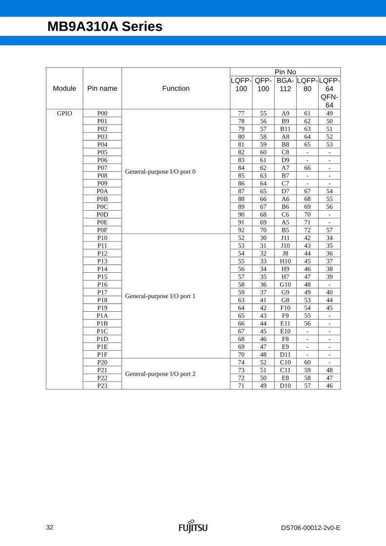
P00 77 55 A9 61 49 P01 78 56 B9 62 50 P02 79 57 B11 63 51 P03 80 58 A8 64 52 P04 81 59 B8 65 53 P05 82 60 C8 - - P06 83 61 D9 - - P07 84 62 A7 66 - P08 85 63 B7 - - P09 86 64 C7 - - P0A 87 65 D7 67 54 P0B 88 66 A6 68 55 P0C 89 67 B6 69 56 P0D 90 68 C6 70 - P0E 91 69 A5 71 - P0F
General-purpose I/O port 0
92 70 B5 72 57 P10 52 30 J11 42 34 P11 53 31 J10 43 35 P12 54 32 J8 44 36 P13 55 33 H10 45 37 P14 56 34 H9 46 38 P15 57 35 H7 47 39 P16 58 36 G10 48 - P17 59 37 G9 49 40 P18 63 41 G8 53 44 P19 64 42 F10 54 45 P1A 65 43 F9 55 - P1B 66 44 E11 56 - P1C 67 45 E10 - - P1D 68 46 F8 - - P1E 69 47 E9 - - P1F
General-purpose I/O port 1
70 48 D11 - - P20 74 52 C10 60 - P21 73 51 C11 59 48 P22 72 50 E8 58 47
GPIO
P23
General-purpose I/O port 2
71 49 D10 57 46

33
FUJITSU SEMICONDUCTOR CONFIDENTIAL r2.1
MB9A310A Series
DS706-00012-2v0-E
Pin No
Module Pin name Function LQFP-
100QFP-100
BGA- 112
LQFP- 80
LQFP-64
QFN-64
P30 9 87 E1 9 5 P31 10 88 E2 10 6 P32 11 89 E3 11 7 P33 12 90 E4 12 8 P34 13 91 F1 - - P35 14 92 F2 - - P36 15 93 F3 - - P37 16 94 G1 - - P38 17 95 G2 - - P39 18 96 F4 13 9 P3A 19 97 G3 14 10 P3B 20 98 H1 15 11 P3C 21 99 H2 16 12 P3D 22 100 G4 17 13 P3E 23 1 H3 18 14 P3F
General-purpose I/O port 3
24 2 J2 19 15 P40 27 5 J4 - - P41 28 6 L5 - - P42 29 7 K5 - - P43 30 8 J5 - - P44 31 9 H5 21 - P45 32 10 L6 22 - P46 36 14 L3 26 19 P47 37 15 K3 27 20 P48 39 17 K6 29 - P49 40 18 J6 30 22 P4A 41 19 L7 31 23 P4B 42 20 K7 32 24 P4C 43 21 H6 33 25 P4D 44 22 J7 34 26 P4E
General-purpose I/O port 4
45 23 K8 35 27 P50 2 80 C1 2 2 P51 3 81 C2 3 3 P52 4 82 B3 4 4 P53 5 83 D1 5 - P54 6 84 D2 6 - P55 7 85 D3 7 - P56
General-purpose I/O port 5
8 86 D5 8 - P60 96 74 C4 76 60 P61 95 73 B4 75 59 P62 94 72 C5 74 58 P63
General-purpose I/O port 6
93 71 D6 73 - P80 98 76 A3 78 62 P81
General-purpose I/O port 8 99 77 A2 79 63
PE0 46 24 K9 36 28 PE2 48 26 L9 38 30
GPIO
PE3 General-purpose I/O port E
49 27 L10 39 31

34
FUJITSU SEMICONDUCTOR CONFIDENTIAL r2.1
MB9A310A Series
DS706-00012-2v0-E
Pin No
Module Pin name Function LQFP-
100QFP-100
BGA- 112
LQFP- 80
LQFP-64
QFN-64
SIN0_0 73 51 C11 59 48 SIN0_1
Multifunction serial interface ch.0 input pin 56 34 H9 46 -
SOT0_0 (SDA0_0)
72 50 E8 58 47
SOT0_1 (SDA0_1)
Multifunction serial interface ch.0 output pin This pin operates as SOT0 when it is used in a UART/CSIO/LIN (operation modes 0 to 3) and as SDA0 when it is used in an I2C (operation mode 4).
57 35 H7 47 -
SCK0_0 (SCL0_0)
71 49 D10 57 46
Multi Function
Serial 0
SCK0_1 (SCL0_1)
Multifunction serial interface ch.0 clock I/O pin This pin operates as SCK0 when it is used in a CSIO (operation modes 2) and as SCL0 when it is used in an I2C (operation mode 4).
58 36 G10 48 -
SIN1_1 Multifunction serial interface ch.1 input pin
53 31 J10 43 35
SOT1_1 (SDA1_1)
Multifunction serial interface ch.1 output pin This pin operates as SOT1 when it is used in a UART/CSIO/LIN (operation modes 0 to 3) and as SDA1 when it is used in an I2C (operation mode 4).
54 32 J8 44 36
Multi Function
Serial 1
SCK1_1 (SCL1_1)
Multifunction serial interface ch.1 clock I/O pin This pin operates as SCK1 when it is used in a CSIO (operation modes 2) and as SCL1 when it is used in an I2C (operation mode 4).
55 33 H10 45 37
35
FUJITSU SEMICONDUCTOR CONFIDENTIAL r2.1
MB9A310A Series
DS706-00012-2v0-E
Pin No
Module Pin name Function LQFP-
100QFP-100
BGA- 112
LQFP- 80
LQFP-64
QFN-64
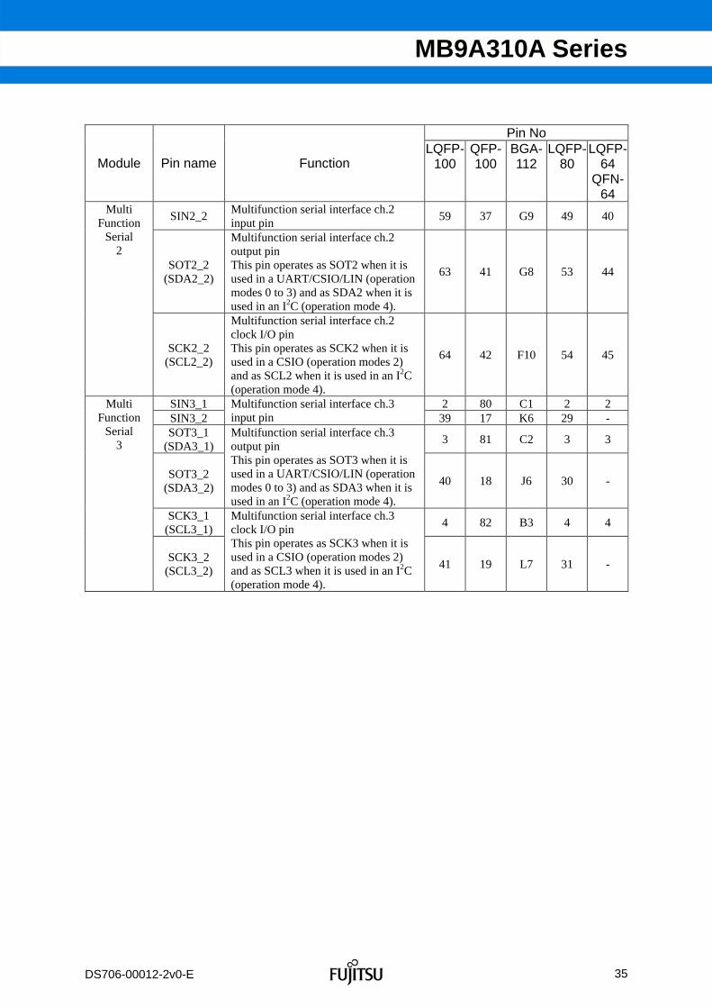
SIN2_2 Multifunction serial interface ch.2 input pin
59 37 G9 49 40
SOT2_2 (SDA2_2)
Multifunction serial interface ch.2 output pin This pin operates as SOT2 when it is used in a UART/CSIO/LIN (operation modes 0 to 3) and as SDA2 when it is used in an I2C (operation mode 4).
63 41 G8 53 44
Multi Function
Serial 2
SCK2_2 (SCL2_2)
Multifunction serial interface ch.2 clock I/O pin This pin operates as SCK2 when it is used in a CSIO (operation modes 2) and as SCL2 when it is used in an I2C (operation mode 4).
64 42 F10 54 45
SIN3_1 2 80 C1 2 2 SIN3_2
Multifunction serial interface ch.3 input pin 39 17 K6 29 -
SOT3_1 (SDA3_1)
3 81 C2 3 3
SOT3_2 (SDA3_2)
Multifunction serial interface ch.3 output pin This pin operates as SOT3 when it is used in a UART/CSIO/LIN (operation modes 0 to 3) and as SDA3 when it is used in an I2C (operation mode 4).
40 18 J6 30 -
SCK3_1 (SCL3_1)
4 82 B3 4 4
Multi Function
Serial 3
SCK3_2 (SCL3_2)
Multifunction serial interface ch.3 clock I/O pin This pin operates as SCK3 when it is used in a CSIO (operation modes 2) and as SCL3 when it is used in an I2C (operation mode 4).
41 19 L7 31 -

36
FUJITSU SEMICONDUCTOR CONFIDENTIAL r2.1
MB9A310A Series
DS706-00012-2v0-E
Pin No
Module Pin name Function LQFP-
100QFP-100
BGA- 112
LQFP- 80
LQFP-64
QFN-64
SIN4_0 87 65 D7 67 54 SIN4_1 65 43 F9 55 - SIN4_2
Multifunction serial interface ch.4 input pin
82 60 C8 - - SOT4_0
(SDA4_0)88 66 A6 68 55
SOT4_1 (SDA4_1)
66 44 E11 56 -
SOT4_2 (SDA4_2)
Multifunction serial interface ch.4 output pin This pin operates as SOT4 when it is used in a UART/CSIO/LIN (operation modes 0 to 3) and as SDA4 when it is used in an I2C (operation mode 4). 83 61 D9 - -
SCK4_0 (SCL4_0)
89 67 B6 69 56
SCK4_1 (SCL4_1)
67 45 E10 - -
SCK4_2 (SCL4_2)
Multifunction serial interface ch.4 clock I/O pin This pin operates as SCK4 when it is used in a CSIO (operation modes 2) and as SCL4 when it is used in an I2C (operation mode 4). 84 62 A7 - -
RTS4_0 90 68 C6 70 - RTS4_1 69 47 E9 - - RTS4_2
Multifunction serial interface ch.4 RTS output pin
86 64 C7 - - CTS4_0 91 69 A5 71 - CTS4_1 68 46 F8 - -
Multi Function
Serial 4
CTS4_2
Multifunction serial interface ch.4 CTS input pin
85 63 B7 - - SIN5_0 96 74 C4 76 60 SIN5_2
Multifunction serial interface ch.5 input pin 15 93 F3 - -
SOT5_0 (SDA5_0)
95 73 B4 75 59
SOT5_2 (SDA5_2)
Multifunction serial interface ch.5 output pin This pin operates as SOT5 when it is used in a UART/CSIO/LIN (operation modes 0 to 3) and as SDA5 when it is used in an I2C (operation mode 4).
16 94 G1 - -
SCK5_0 (SCL5_0)
94 72 C5 74 58
Multi Function
Serial 5
SCK5_2 (SCL5_2)
Multifunction serial interface ch.5 clock I/O pin This pin operates as SCK5 when it is used in a CSIO (operation modes 2) and as SCL5 when it is used in an I2C (operation mode 4).
17 95 G2 - -

37
FUJITSU SEMICONDUCTOR CONFIDENTIAL r2.1
MB9A310A Series
DS706-00012-2v0-E
Pin No
Module Pin name Function LQFP-
100QFP-100
BGA- 112
LQFP- 80
LQFP-64
QFN-64
SIN6_0 5 83 D1 5 - SIN6_1
Multifunction serial interface ch.6 input pin 12 90 E4 12 8
SOT6_0 (SDA6_0)
6 84 D2 6 -
SOT6_1 (SDA6_1)
Multifunction serial interface ch.6 output pin This pin operates as SOT6 when it is used in a UART/CSIO/LIN (operation modes 0 to 3) and as SDA6 when it is used in an I2C (operation mode 4).
11 89 E3 11 7
SCK6_0 (SCL6_0)
7 85 D3 7 -
Multi Function
Serial 6
SCK6_1 (SCL6_1)
Multifunction serial interface ch.6 clock I/O pin This pin operates as SCK6 when it is used in a CSIO (operation modes 2) and as SCL6 when it is used in an I2C (operation mode 4).
10 88 E2 10 6
SIN7_1 Multifunction serial interface ch.7 input pin
45 23 K8 35 27
SOT7_1 (SDA7_1)
Multifunction serial interface ch.7 output pin This pin operates as SOT7 when it is used in a UART/CSIO/LIN (operation modes 0 to 3) and as SDA7 when it is used in an I2C (operation mode 4).
44 22 J7 34 26
Multi Function
Serial 7
SCK7_1 (SCL7_1)
Multifunction serial interface ch.7 clock I/O pin This pin operates as SCK7 when it is used in a CSIO (operation modes 2) and as SCL7 when it is used in an I2C (operation mode 4).
43 21 H6 33 25

38
FUJITSU SEMICONDUCTOR CONFIDENTIAL r2.1
MB9A310A Series
DS706-00012-2v0-E
Pin No
Module Pin name Function LQFP-
100QFP-100
BGA- 112
LQFP- 80
LQFP-64
QFN-64
DTTI0X_0 18 96 F4 13 9
DTTI0X_1
Input signal of wave form generator to control outputs RTO00 to RTO05 of multi-function timer 0 69 47 E9 - -
FRCK0_0 13 91 F1 - - FRCK0_1 70 48 D11 - - FRCK0_2
16-bit free-run timer ch.0 external clock input pin
53 31 J10 43 35 IC00_0 17 95 G2 - - IC00_1 65 43 F9 55 - IC00_2 54 32 J8 44 36 IC01_0 16 94 G1 - - IC01_1 66 44 E11 56 - IC01_2 55 33 H10 45 37 IC02_0 15 93 F3 - - IC02_1 67 45 E10 - - IC02_2 56 34 H9 46 38 IC03_0 14 92 F2 - - IC03_1 68 46 F8 - - IC03_2
16-bit input capture input pin of multi-function timer 0 ICxx describes channel number.
57 35 H7 47 39 RTO00_0
(PPG00_0)19 97 G3 14 10
RTO00_1 (PPG00_1)
Wave form generator output of multi-function timer 0 This pin operates as PPG00 when it is used in PPG 0 output modes. 71 49 D10 - -
RTO01_0 (PPG00_0)
Wave form generator output of multi-function timer 0 This pin operates as PPG00 when it is used in PPG 0 output modes.
20 98 H1 15 11
RTO02_0 (PPG02_0)
Wave form generator output of multi-function timer 0 This pin operates as PPG02 when it is used in PPG 0 output modes.
21 99 H2 16 12
RTO03_0 (PPG02_0)
Wave form generator output of multi-function timer 0 This pin operates as PPG02 when it is used in PPG 0 output modes.
22 100 G4 17 13
RTO04_0 (PPG04_0)
Wave form generator output of multi-function timer 0 This pin operates as PPG04 when it is used in PPG 0 output modes.
23 1 H3 18 14
Multi Function
Timer 0
RTO05_0 (PPG04_0)
Wave form generator output of multi-function timer 0 This pin operates as PPG04 when it is used in PPG 0 output modes.
24 2 J2 19 15

39
FUJITSU SEMICONDUCTOR CONFIDENTIAL r2.1
MB9A310A Series
DS706-00012-2v0-E
Pin No
Module Pin name Function LQFP-
100QFP-100
BGA- 112
LQFP- 80
LQFP-64
QFN-64
DTTI1X_0 8 86 D5 8 -
DTTI1X_1
Input signal of wave form generator to control outputs RTO10 to RTO15 of multi-function timer 1 39 17 K6 29 -
FRCK1_0 87 65 D7 67 - FRCK1_1
16-bit free-run timer ch.1 external clock input pin 44 22 J7 34 -
IC10_0 88 66 A6 68 - IC10_1 40 18 J6 30 - IC11_0 89 67 B6 69 - IC11_1 41 19 L7 31 - IC12_0 90 68 C6 70 - IC12_1 42 20 K7 32 - IC13_0 91 69 A5 71 - IC13_1
16-bit input capture input pin of multi-function timer 1 ICxx describes channel number.
43 21 H6 33 - RTO10_0
(PPG10_0)2 80 C1 2 -
RTO10_1 (PPG10_1)
Wave form generator output of multi-function timer 1 This pin operates as PPG10 when it is used in PPG 1 output modes. 27 5 J4 - -
RTO11_0 (PPG10_0)
3 81 C2 3 -
RTO11_1 (PPG10_1)
Wave form generator output of multi-function timer 1 This pin operates as PPG10 when it is used in PPG 1 output modes. 28 6 L5 - -
RTO12_0 (PPG12_0)
4 82 B3 4 -
RTO12_1 (PPG12_1)
Wave form generator output of multi-function timer 1 This pin operates as PPG12 when it is used in PPG 1 output modes. 29 7 K5 - -
RTO13_0 (PPG12_0)
5 83 D1 5 -
RTO13_1 (PPG12_1)
Wave form generator output of multi-function timer 1 This pin operates as PPG12 when it is used in PPG 1 output modes. 30 8 J5 - -
RTO14_0 (PPG14_0)
6 84 D2 6 -
RTO14_1 (PPG14_1)
Wave form generator output of multi-function timer 1 This pin operates as PPG14 when it is used in PPG 1 output modes. 31 9 H5 21 -
RTO15_0 (PPG14_0)
7 85 D3 7 -
Multi Function
Timer 1
RTO15_1 (PPG14_1)
Wave form generator output of multi-function timer 1 This pin operates as PPG14 when it is used in PPG 1 output modes. 32 10 L6 22 -

40
FUJITSU SEMICONDUCTOR CONFIDENTIAL r2.1
MB9A310A Series
DS706-00012-2v0-E
Pin No
Module Pin name Function LQFP-
100QFP-100
BGA- 112
LQFP- 80
LQFP-64
QFN-64
AIN0_0 9 87 E1 9 5 AIN0_1 40 18 J6 30 22 AIN0_2
QPRC ch.0 AIN input pin 2 80 C1 2 2
BIN0_0 10 88 E2 10 6 BIN0_1 41 19 L7 31 23 BIN0_2
QPRC ch.0 BIN input pin 3 81 C2 3 3
ZIN0_0 11 89 E3 11 7 ZIN0_1 42 20 K7 32 24
Quadrature Position/
Revolution Counter
0
ZIN0_2 QPRC ch.0 ZIN input pin
4 82 B3 4 4 AIN1_1 74 52 C10 60 - AIN1_2
QPRC ch.1 AIN input pin 43 21 H6 33 25
BIN1_1 73 51 C11 59 - BIN1_2
QPRC ch.1 BIN input pin 44 22 J7 34 26
ZIN1_1 72 50 E8 58 -
Quadrature Position/
Revolution Counter
1
ZIN1_2 QPRC ch.1 ZIN input pin
45 23 K8 35 27 UDM0 USB Function / HOST D – pin 98 76 A3 78 62 UDP0 USB Function / HOST D + pin 99 77 A2 79 63
USB
UHCONX USB external pull-up control pin 95 73 B4 75 59

41
FUJITSU SEMICONDUCTOR CONFIDENTIAL r2.1
MB9A310A Series
DS706-00012-2v0-E
Pin No
Module Pin name Function LQFP-
100QFP-100
BGA- 112
LQFP- 80
LQFP-64
QFN-64
RESET INITX
External Reset Input. A reset is valid when INITX=L
38 16 K4 28 21
MD0
Mode 0 pin During normal operation, MD0=L must be input. During serial programming to flash memory, MD0=H must be input.
47 25 L8 37 29
Mode
MD1 Mode 1 pin During serial programming to flash memory, MD1=L must be input.
46 24 K9 36 28
VCC Power supply Pin 1 79 B1 1 1 VCC Power supply Pin 26 4 J1 - - VCC Power supply pin 35 13 K1 25 18 VCC Power supply pin 51 29 K11 41 33 VCC Power supply pin 76 54 A10 - -
POWER
USBVCC 3.3V Power supply port for USB I/O 97 75 A4 77 61 VSS GND Pin - - B2 - - VSS GND pin 25 3 L1 20 16 VSS GND pin - - K2 - - VSS GND pin - - J3 - - VSS GND pin - - H4 - - VSS GND pin 34 12 L4 24 - VSS GND pin 50 28 L11 40 32 VSS GND pin - - K10 - - VSS GND pin - - J9 - - VSS GND pin - - H8 - - VSS GND pin - - B10 - - VSS GND pin - - C9 - - VSS GND pin 75 53 A11 - - VSS GND pin - - D8 - - VSS GND pin - - D4 - - VSS GND pin - - C3 - -
GND
VSS GND pin 100 78 A1 80 64 X0 Main clock (oscillation) input pin 48 26 L9 38 30
X0A Sub clock (oscillation) input pin 36 14 L3 26 19 X1 Main clock (oscillation) I/O pin 49 27 L10 39 31
X1A Sub clock (oscillation) I/O pin 37 15 K3 27 20 CROUT_0 74 52 C10 60 -
CLOCK
CROUT_1Built-in high-speed CR-osc clock output port 92 70 B5 72 57
AVCC A/D converter analog power supply pin
60 38 H11 50 41 ADC
POWER
AVRH A/D converter analog reference voltage input pin
61 39 F11 51 42
ADC GND
AVSS A/D converter GND pin 62 40 G11 52 43
C pin C Power stabilization capacity pin 33 11 L2 23 17

42
FUJITSU SEMICONDUCTOR CONFIDENTIAL r2.1
MB9A310A Series
DS706-00012-2v0-E
I/O CIRCUIT TYPE Type Circuit Remarks
A It is possible to select the main oscillation / GPIO function
When the main oscillation is selected. Oscillation feedback resistor
: Approximately 1MΩ With Standby mode control
When the GPIO is selected. CMOS level output. CMOS level hysteresis input With pull-up resistor control With standby mode control Pull-up resistor
: Approximately 50kΩ IOH = -4mA, IOL = 4mA
B
CMOS level hysteresis input Pull-up resistor
: Approximately 50kΩ
Standby mode control
Standby mode control
Digital output
Digital output
Standby mode control
X0
Clock input
Digital input
P-ch
N-ch
Digital input
Digital output
Digital outputP-ch
N-ch
X1
R
R
P-ch
Pull-up resistor control
P-ch
Pull-up resistor control
Pull-up resistor
Digital input

43
FUJITSU SEMICONDUCTOR CONFIDENTIAL r2.1
MB9A310A Series
DS706-00012-2v0-E
Type Circuit Remarks C
N-ch
Open drain output CMOS level hysteresis input
D
It is possible to select the sub oscillation / GPIO function
When the sub oscillation is selected. Oscillation feedback resistor
: Approximately 5MΩ With Standby mode control When the GPIO is selected. CMOS level output. CMOS level hysteresis input With pull-up resistor control With standby mode control Pull-up resistor
: Approximately 50kΩ IOH = -4mA, IOL = 4mA
Standby mode control
Standby mode control
Digital output
Digital output
Standby mode control
X0A
Clock input
Digital input
P-ch
N-ch
Digital input
Digital output
Digital outputP-ch
N-ch
X1A
R
R
P-ch
Pull-up resistor control
P-ch
Pull-up resistor control
Digital input
Digital output

44
FUJITSU SEMICONDUCTOR CONFIDENTIAL r2.1
MB9A310A Series
DS706-00012-2v0-E
Type Circuit Remarks E
CMOS level output CMOS level hysteresis input With pull-up resistor control With standby mode control Pull-up resistor
: Approximately 50kΩ IOH = -4mA, IOL = 4mA
F
CMOS level output CMOS level hysteresis input With input control Analog input With pull-up resistor control With standby mode control Pull-up resistor
: Approximately 50kΩ IOH = -4mA, IOL = 4mA
Standby mode control
Digital output
Pull-up resistor control
Digital output
Digital input
P-ch P-ch
N-ch
Digital output
Digital output
Pull-up resistor control
Input control
Standby mode control
Analog input
Digital input
P-ch P-ch
N-ch
R
R

45
FUJITSU SEMICONDUCTOR CONFIDENTIAL r2.1
MB9A310A Series
DS706-00012-2v0-E
Type Circuit Remarks G
CMOS level output CMOS level hysteresis input With pull-up resistor control With standby mode control Pull-up resistor
: Approximately 50kΩ IOH = -12mA, IOL = 12mA
H
DifferentialDifferential input
UDP(+)input
UDM(-)input
USB/GPIO select
GPIO Digital input
GPIO Digital input
GPIO Digital input circuit control
GPIO Digital input/output direction
GPIO Digital output
USB input/output direction
UDM(-)output
UDP(+)output
USB full-speed, low-speed control
GPIO Digital input circuit control
GPIO Digital input/output direction
GPIO Digital output
EBP
EBM
It is possible to select the USB IO / GPIO function.
When the USB IO is selected. Full-speed, Low-speed control When the GPIO is selected. CMOS level output CMOS level hysteresis input With standby mode control IOH = -20.5mA, IOL = 18.5mA
Standby mode control
Digital output
Pull-up resistor control
Digital output
Digital input
P-ch P-ch
N-ch
R

46
FUJITSU SEMICONDUCTOR CONFIDENTIAL r2.1
MB9A310A Series
DS706-00012-2v0-E
Type Circuit Remarks I
P-ch
N-ch
CMOS level output CMOS level hysteresis input 5V tolerant With standby mode control IOH = -4mA, IOL = 4mA
J
Mode Input
CMOS level hysteresis input
Digital input
Standby mode control
Digital output
Digital output
R

47
FUJITSU SEMICONDUCTOR CONFIDENTIAL r1.0
MB9A310A Series
DS706-00012-2v0-E
HANDLING PRECAUTIONS Any semiconductor devices have inherently a certain rate of failure. The possibility of failure is greatly affected by the conditions in which they are used (circuit conditions, environmental conditions, etc.). This page describes precautions that must be observed to minimize the chance of failure and to obtain higher reliability from your FUJITSU SEMICONDUCTOR semiconductor devices.
1. Precautions for Product Design This section describes precautions when designing electronic equipment using semiconductor devices.
Absolute Maximum Ratings Semiconductor devices can be permanently damaged by application of stress (voltage, current, temperature, etc.) in excess of certain established limits, called absolute maximum ratings. Do not exceed these ratings.
Recommended Operating Conditions Recommended operating conditions are normal operating ranges for the semiconductor device. All the device's electrical characteristics are warranted when operated within these ranges.
Always use semiconductor devices within the recommended operating conditions. Operation outside these ranges may adversely affect reliability and could result in device failure.
No warranty is made with respect to uses, operating conditions, or combinations not represented on the data sheet. Users considering application outside the listed conditions are advised to contact their sales representative beforehand.
Processing and Protection of Pins These precautions must be followed when handling the pins which connect semiconductor devices to power supply and input/output functions.
(1) Preventing Over-Voltage and Over-Current Conditions Exposure to voltage or current levels in excess of maximum ratings at any pin is likely to cause deterioration within the device, and in extreme cases leads to permanent damage of the device. Try to prevent such overvoltage or over-current conditions at the design stage.
(2) Protection of Output Pins Shorting of output pins to supply pins or other output pins, or connection to large capacitance can cause large current flows. Such conditions if present for extended periods of time can damage the device. Therefore, avoid this type of connection.
(3) Handling of Unused Input Pins Unconnected input pins with very high impedance levels can adversely affect stability of operation. Such pins should be connected through an appropriate resistance to a power supply pin or ground pin.
Latch-up Semiconductor devices are constructed by the formation of P-type and N-type areas on a substrate. When subjected to abnormally high voltages, internal parasitic PNPN junctions (called thyristor structures) may be formed, causing large current levels in excess of several hundred mA to flow continuously at the power supply pin. This condition is called latch-up.
CAUTION: The occurrence of latch-up not only causes loss of reliability in the semiconductor device, but can cause injury or damage from high heat, smoke or flame. To prevent this from happening, do the following:
(1) Be sure that voltages applied to pins do not exceed the absolute maximum ratings. This should include attention to abnormal noise, surge levels, etc.
(2) Be sure that abnormal current flows do not occur during the power-on sequence.
Code: DS00-00004-1Ea

48
FUJITSU SEMICONDUCTOR CONFIDENTIAL r1.0
MB9A310A Series
DS706-00012-2v0-E
Observance of Safety Regulations and Standards Most countries in the world have established standards and regulations regarding safety, protection from electromagnetic interference, etc. Customers are requested to observe applicable regulations and standards in the design of products.
Fail-Safe Design Any semiconductor devices have inherently a certain rate of failure. You must protect against injury, damage or loss from such failures by incorporating safety design measures into your facility and equipment such as redundancy, fire protection, and prevention of over-current levels and other abnormal operating conditions.
Precautions Related to Usage of Devices FUJITSU SEMICONDUCTOR semiconductor devices are intended for use in standard applications (computers, office automation and other office equipment, industrial, communications, and measurement equipment, personal or household devices, etc.).
CAUTION: Customers considering the use of our products in special applications where failure or abnormal operation may directly affect human lives or cause physical injury or property damage, or where extremely high levels of reliability are demanded (such as aerospace systems, atomic energy controls, sea floor repeaters, vehicle operating controls, medical devices for life support, etc.) are requested to consult with sales representatives before such use. The company will not be responsible for damages arising from such use without prior approval.
2. Precautions for Package Mounting Package mounting may be either lead insertion type or surface mount type. In either case, for heat resistance during soldering, you should only mount under FUJITSU SEMICONDUCTOR's recommended conditions. For detailed information about mount conditions, contact your sales representative.
Lead Insertion Type Mounting of lead insertion type packages onto printed circuit boards may be done by two methods: direct soldering on the board, or mounting by using a socket.
Direct mounting onto boards normally involves processes for inserting leads into through-holes on the board and using the flow soldering (wave soldering) method of applying liquid solder. In this case, the soldering process usually causes leads to be subjected to thermal stress in excess of the absolute ratings for storage temperature. Mounting processes should conform to FUJITSU SEMICONDUCTOR recommended mounting conditions.
If socket mounting is used, differences in surface treatment of the socket contacts and IC lead surfaces can lead to contact deterioration after long periods. For this reason it is recommended that the surface treatment of socket contacts and IC leads be verified before mounting.
Surface Mount Type Surface mount packaging has longer and thinner leads than lead-insertion packaging, and therefore leads are more easily deformed or bent. The use of packages with higher pin counts and narrower pin pitch results in increased susceptibility to open connections caused by deformed pins, or shorting due to solder bridges.
You must use appropriate mounting techniques. FUJITSU SEMICONDUCTOR recommends the solder reflow method, and has established a ranking of mounting conditions for each product. Users are advised to mount packages in accordance with FUJITSU SEMICONDUCTOR ranking of recommended conditions.

49
FUJITSU SEMICONDUCTOR CONFIDENTIAL r1.0
MB9A310A Series
DS706-00012-2v0-E
Lead-Free Packaging CAUTION: When ball grid array (BGA) packages with Sn-Ag-Cu balls are mounted using Sn-Pb eutectic soldering, junction strength may be reduced under some conditions of use.
Storage of Semiconductor Devices Because plastic chip packages are formed from plastic resins, exposure to natural environmental conditions will cause absorption of moisture. During mounting, the application of heat to a package that has absorbed moisture can cause surfaces to peel, reducing moisture resistance and causing packages to crack. To prevent, do the following:
(1) Avoid exposure to rapid temperature changes, which cause moisture to condense inside the product. Store products in locations where temperature changes are slight.
(2) Use dry boxes for product storage. Products should be stored below 70% relative humidity, and at temperatures between 5°C and 30°C. When you open Dry Package that recommends humidity 40% to 70% relative humidity.
(3) When necessary, FUJITSU SEMICONDUCTOR packages semiconductor devices in highly moisture-resistant aluminum laminate bags, with a silica gel desiccant. Devices should be sealed in their aluminum laminate bags for storage.
(4) Avoid storing packages where they are exposed to corrosive gases or high levels of dust.
Baking Packages that have absorbed moisture may be de-moisturized by baking (heat drying). Follow the FUJITSU SEMICONDUCTOR recommended conditions for baking.
Condition: 125°C/24 h
Static Electricity Because semiconductor devices are particularly susceptible to damage by static electricity, you must take the following precautions:
(1) Maintain relative humidity in the working environment between 40% and 70%. Use of an apparatus for ion generation may be needed to remove electricity.
(2) Electrically ground all conveyors, solder vessels, soldering irons and peripheral equipment.
(3) Eliminate static body electricity by the use of rings or bracelets connected to ground through high resistance (on the level of 1 MΩ). Wearing of conductive clothing and shoes, use of conductive floor mats and other measures to minimize shock loads is recommended.
(4) Ground all fixtures and instruments, or protect with anti-static measures.
(5) Avoid the use of styrofoam or other highly static-prone materials for storage of completed board assemblies.

50
FUJITSU SEMICONDUCTOR CONFIDENTIAL r1.0
MB9A310A Series
DS706-00012-2v0-E
3. Precautions for Use Environment Reliability of semiconductor devices depends on ambient temperature and other conditions as described above.
For reliable performance, do the following:
(1) Humidity Prolonged use in high humidity can lead to leakage in devices as well as printed circuit boards. If high humidity levels are anticipated, consider anti-humidity processing.
(2) Discharge of Static Electricity When high-voltage charges exist close to semiconductor devices, discharges can cause abnormal operation. In such cases, use anti-static measures or processing to prevent discharges.
(3) Corrosive Gases, Dust, or Oil Exposure to corrosive gases or contact with dust or oil may lead to chemical reactions that will adversely affect the device. If you use devices in such conditions, consider ways to prevent such exposure or to protect the devices.
(4) Radiation, Including Cosmic Radiation Most devices are not designed for environments involving exposure to radiation or cosmic radiation. Users should provide shielding as appropriate.
(5) Smoke, Flame CAUTION: Plastic molded devices are flammable, and therefore should not be used near combustible substances. If devices begin to smoke or burn, there is danger of the release of toxic gases. Customers considering the use of FUJITSU SEMICONDUCTOR products in other special environmental conditions should consult with sales representatives.
Please check the latest handling precautions at the following URL. http://edevice.fujitsu.com/fj/handling-e.pdf

51
FUJITSU SEMICONDUCTOR CONFIDENTIAL r1.0
MB9A310A Series
DS706-00012-2v0-E
HANDLING DEVICES Power supply pins
In products with multiple VCC and VSS pins, respective pins at the same potential are interconnected within the device in order to prevent malfunctions such as latch-up. However, all of these pins should be connected externally to the power supply or ground lines in order to reduce electromagnetic emission levels, to prevent abnormal operation of strobe signals caused by the rise in the ground level, and to conform to the total output current rating.
Moreover, connect the current supply source with each Power supply pin and GND pin of this device at low impedance. It is also advisable that a ceramic capacitor of approximately 0.1 µF be connected as a bypass capacitor between each Power supply pin and GND pin near this device.
Crystal oscillator circuit Noise near the X0/X1 and X0A/X1A pins may cause the device to malfunction. Design the printed circuit board so that X0/X1, X0A/X1A pins, the crystal oscillator, and the bypass capacitor to ground are located as close to the device as possible.
It is strongly recommended that the PC board artwork be designed such that the X0/X1 and X0A/X1A pins are surrounded by ground plane as this is expected to produce stable operation.
Using an external clock When using an external clock, the clock signal should be driven to the X0,X0A pin only and the X1,X1A pin should be kept open.
Handling when using Multi function serial pin as I2C pin If it is using the multi function serial pin as I2C pins, P-ch transistor of digital output is always disabled. However, I2C pins need to keep the electrical characteristic like other pins and not to connect to the external I2C bus system with power OFF.
Example of Using an External Clock Device
X0(X0A)
X1(X1A)Open

52
FUJITSU SEMICONDUCTOR CONFIDENTIAL r1.0
MB9A310A Series
DS706-00012-2v0-E
C Pin As this series includes a built-in regulator, always connect a bypass capacitor of approximately 4.7 µF to the C pin for use by the regulator.
Mode pins (MD0) Connect the MD pin (MD0) directly to VCC or VSS pins. Design the printed circuit board such that the pull-up/down resistor stays low, as well as the distance between the mode pins and VCC pins or VSS pins is as short as possible and the connection impedance is low, when the pins are pulled-up/down such as for switching the pin level and rewriting the Flash memory data. It is because of preventing the device erroneously switching to test mode due to noise.
Notes on power-on Turn power on/off in the following order or at the same time. If not using the A/D converter, connect AVCC = VCC and AVSS = VSS.
Turning on : VCC → USBVCC
VCC → AVCC → AVRH
Turning off : USBVCC → VCC
AVRH → AVCC → VCC
Serial Communication There is a possibility to receive wrong data due to the noise or other causes on the serial communication. Therefore, design a printed circuit board so as to avoid noise. Consider the case of receiving wrong data due to noise, perform error detection such as by applying a checksum of data at the end. If an error is detected, retransmit the data.
Differences in features among the products with different memory sizes and between
Flash products and MASK products The electric characteristics including power consumption, ESD, latch-up, noise characteristics, and oscillation characteristics among the products with different memory sizes and between Flash products and MASK products are different because chip layout and memory structures are different.
If you are switching to use a different product of the same series, please make sure to evaluate the electric characteristics.
Device
C
VSS
4.7μF
GND

53
FUJITSU SEMICONDUCTOR CONFIDENTIAL r2.0
MB9A310A Series
DS706-00012-2v0-E
BLOCK DIAGRAM
Flash I/FCortex-M3 Core@40 MHz(Max)
Clock ResetGenerator
Dual-Timer
WatchDog Timer(Hardware)
DMAC 8ch
Multi-Function Timer x 2
Multi-Function Serial I/F 8ch.
(with FIFO ch.4 to 7)& HW flow control(ch.4)*2
16-bit Free-Run Timer3ch.
16-bit Output Compare
6ch.
16-bit Input Capture4ch.
Waveform Generator3ch.
A/D Activation Compare
3ch.
16-bit PPG3ch.
Watch Counter
Unit 0
GPIO
CSV
MainOsc
PLL
LVD
External Interrupt Controller
16-pin + NMI
Power-OnReset
TPIU*1 ROMTable
ETM*1 SRAM08/16
Kbyte
SWJ-DP
SRAM18/16
Kbyte
I
D
Sys
CLK RST
Base Timer16-bit 8ch. /32-bit 4ch.
NVIC
WatchDog Timer(Software)
Security
SubOsc
CR 4 MHz
12-bit A/D Converter x 3
Unit 1
Unit 2*2
TRSTX,TCK,TDI,TMS
TRACED[3:0],TRACECLK
X0
AVCC,AVSS,AVRH
AN[15:0]
TIOA[7:0]
TIOB[7:0]
IC0[3:0]
DTTI[1:0]XRTO0[5:0]
FRCK[1:0]
C
TDO
X1
X0A
X1A
SCK[7:0]
SIN[7:0]
SOT[7:0]
INT[15:0]
NMIX
P0[F:0],P1[F:0],
.
.
.Px[x:0]
INITX
MODE-Ctrl
IRQ-Monitor
PIN-Function-Ctrl
MD[1:0]
CR 100 kHz
Regulator
QPRC2ch.
AIN[1:0]
BIN[1:0]
ZIN[1:0]
LVD Ctrl
CRC Accelerator
IC1[3:0]
ADTGx
RTS4CTS4
External Bus I/F*2
MAD[24:0]
MADATA[15:0]
MCSX[7:0],MOEX,MWEX,MALE,MRDY,MCLKOUT,MDQM[1:0]
RTO1[5:0]
On-ChipFlash
64/128/256/384/512Kbyte
USB2.0 (Host/ Func)
PHY USBVCC
UDP0/UDM0
UHCONX
*1: For the MB9AF311LA/MA, F312LA/MA, MB9AF314LA/MA, MB9AF315MA and MB9AF316MA, ETM
is not available. *2: For the MB9AF311LA, F312LA and MB9AF314LA, the External Bus Interface and 12-bit A/D Converter
(unit 2) are not available. And the Multi-function Serial Interface does not support hardware flow control in these products.
54
FUJITSU SEMICONDUCTOR CONFIDENTIAL r2.0
DS706-00012-2v0-E
MB9A310A Series
MEMORY SIZE See "Memory size" in "PRODUCT LINEUP" to confirm the memory size.

55
FUJITSU SEMICONDUCTOR CONFIDENTIAL r2.0
MB9A310A Series
DS706-00012-2v0-E
MEMORY MAP MB9A310A Series Memory Map(1)
Peripherals Area0x41FF_FFFF
0xFFFF_FFFF
0xE010_0000
0x4006_1000
0xE000_0000 0x4006_0000 DMAC
0x4005_0000 Reserved
0x4004_0000 USB ch.0
0x4003_F000 EXT-bus I/F
0x4003_B000
0x4003_A000 Watch Counter
0x4003_9000 CRC
0x4003_8000 MFS
0x6000_0000 0x4003_7000 Reserved
0x4003_6000 USB Clock Ctrl
0x4003_5000 LVD
0x4400_0000
0x4003_4000
0x4200_0000 0x4003_3000 GPIO
0x4003_2000 Reserved
0x4000_0000 0x4003_1000 Int-Req.Read
0x4003_0000 EXTI
0x4002_F000 Reserved
0x2400_0000 0x4002_E000 CR Trim
0x2200_0000 0x4002_8000
0x4002_7000 A/DC
0x4002_6000 QPRC
0x2008_0000 0x4002_5000 Base Timer
0x2000_0000 SRAM1 PPG
0x1FF8_0000 SRAM0
0x4002_2000
0x0010_2000 0x4002_1000 MFT Unit1
0x0010_0000 Security/CR Trim 0x4002_0000 MFT Unit0
0x4001_6000
0x4001_5000 Dual Timer
0x4001_3000
0x0000_0000 0x4001_2000 SW WDT0x4001_1000 HW WDT0x4001_0000 Clock/Reset
0x4000_1000
0x4000_0000 Flash I/F
Reserved
Peripherals
Reserved
32MbytesBit band alias
Reserved
Reserved
See the next page"Memory Map (2),(3)"for the memory sizedetails.
ReservedReserved
FlashReserved
Reserved
Reserved32Mbytes
Bit band alias
Reserved
Reserved
Cortex-M3 PrivatePeripherals
External DeviceArea
Reserved

56
FUJITSU SEMICONDUCTOR CONFIDENTIAL r2.0
DS706-00012-2v0-E
MB9A310A Series
MB9A310A Series Memory Map(2)
MB9AF316MA/NA MB9AF315MA/NA MB9AF314LA/MA/NA
0x2008_0000 0x2008_0000 0x2008_0000
0x2000_4000 0x2000_4000 0x2000_4000
0x2000_0000 0x2000_0000 0x2000_0000
0x1FFF_C000 0x1FFF_C000 0x1FFF_C000
0x0010_2000 0x0010_2000 0x0010_2000
0x0010_1000 CR trimming 0x0010_1000 CR trimming 0x0010_1000 CR trimming
0x0010_0000 Security 0x0010_0000 Security 0x0010_0000 Security
0x0008_0000
0x0006_0000
0x0004_0000
0x0000_0000 0x0000_0000 0x0000_0000
Reserved
SRAM016Kbytes
SRAM116Kbytes
Reserved
SRAM116Kbytes
Flash 256Kbytes
Reserved
Flash 512Kbytes
Flash 384Kbytes
Reserved
Reserved
SRAM016Kbytes
Reserved
Reserved
SRAM116Kbytes
SRAM016Kbytes
Reserved
Reserved

57
FUJITSU SEMICONDUCTOR CONFIDENTIAL r2.0
MB9A310A Series
DS706-00012-2v0-E
MB9A310A Series Memory Map(3)
MB9AF312LA/MA/NA MB9AF311LA/MA/NA
0x2008_0000 0x2008_0000
0x2000_2000 0x2000_2000
0x2000_0000 0x2000_0000
0x1FFF_E000 0x1FFF_E000
0x0010_2000 0x0010_2000
0x0010_1000 CR trimming 0x0010_1000 CR trimming
0x0010_0000 Security 0x0010_0000 Security
0x0008_0000 0x0008_0000
0x0002_0000
0x0001_0000
0x0000_0000 0x0000_0000
SRAM08Kbytes
SRAM08Kbytes
Reserved
SRAM18Kbytes
Reserved
SRAM18Kbytes
Flash 64Kbytes
Reserved
Flash 128Kbytes
Reserved
ReservedReserved

58
FUJITSU SEMICONDUCTOR CONFIDENTIAL r2.0
DS706-00012-2v0-E
MB9A310A Series
Peripheral Address Map
Start address End address Bus Peripherals
0x4000_0000H 0x4000_0FFFH Flash I/F register
0x4000_1000H 0x4000_FFFFH AHB
Reserved
0x4001_0000H 0x4001_0FFFH Clock/Reset Control
0x4001_1000H 0x4001_1FFFH Hardware Watchdog timer
0x4001_2000H 0x4001_2FFFH Software Watchdog timer
0x4001_3000H 0x4001_4FFFH Reserved
0x4001_5000H 0x4001_5FFFH Dual-Timer
0x4001_6000H 0x4001_FFFFH
APB0
Reserved
0x4002_0000H 0x4002_0FFFH Multi-function timer unit0
0x4002_1000H 0x4002_1FFFH Multi-function timer unit1
0x4002_2000H 0x4002_3FFFH Reserved
0x4002_4000H 0x4002_4FFFH PPG
0x4002_5000H 0x4002_5FFFH Base Timer
0x4002_6000H 0x4002_6FFFH Quadrature Position/Revolution Counter
0x4002_7000H 0x4002_7FFFH A/D Converter
0x4002_8000H 0x4002_DFFFH Reserved
0x4002_E000H 0x4002_EFFFH Built-in CR trimming
0x4002_F000H 0x4002_FFFFH
APB1
Reserved
0x4003_0000H 0x4003_0FFFH External Interrupt Controller
0x4003_1000H 0x4003_1FFFH Interrupt Source Check Register
0x4003_2000H 0x4003_2FFFH Reserved
0x4003_3000H 0x4003_3FFFH GPIO
0x4003_4000H 0x4003_4FFFH Reserved
0x4003_5000H 0x4003_5FFFH Low-Voltage Detector
0x4003_6000H 0x4003_6FFFH USB clock generator
0x4003_7000H 0x4003_7FFFH Reserved
0x4003_8000H 0x4003_8FFFH Multi-function serial
0x4003_9000H 0x4003_9FFFH CRC
0x4003_A000H 0x4003_AFFFH Watch Counter
0x4003_B000H 0x4003_EFFFH Reserved
0x4003_F000H 0x4003_FFFFH
APB2
External bus interface
0x4004_0000H 0x4004_FFFFH USB ch.0
0x4005_0000H 0x4005_FFFFH Reserved
0x4006_0000H 0x4006_0FFFH DMAC register
0x4006_1000H 0x4006_1FFFH Reserved
0x4006_2000H 0x4006_2FFFH Reserved
0x4006_3000H 0x4006_3FFFH Reserved
0x4006_4000H 0x41FF_FFFFH
AHB
Reserved
59
FUJITSU SEMICONDUCTOR CONFIDENTIAL r2.0
MB9A310A Series
DS706-00012-2v0-E
PIN STATUS IN EACH CPU STATE The terms used for pin status have the following meanings.
INITX = 0
This is the period when the INITX pin is the "L" level.
INITX = 1
This is the period when the INITX pin is the "H" level.
SPL = 0
This is the status that the standby pin level setting bit (SPL) in the standby mode control register (STB_CTL) is set to "0".
SPL = 1
This is the status that the standby pin level setting bit (SPL) in the standby mode control register (STB_CTL) is set to "1".
Input enabled
Indicates that the input function can be used.
Internal input fixed at "0"
This is the status that the input function cannot be used. Internal input is fixed at "L".
Hi-Z
Indicates that the pin drive transistor is disabled and the pin is put in the Hi-Z state.
Setting disabled
Indicates that the setting is disabled.
Maintain previous state
Maintains the state that was immediately prior to entering the current mode. If a built-in peripheral function is operating, the output follows the peripheral function. If the pin is being used as a port, that output is maintained.
Analog input is enabled
Indicates that the analog input is enabled.
Trace output
Indicates that the trace function can be used.

60
FUJITSU SEMICONDUCTOR CONFIDENTIAL r2.0
MB9A310A Series
DS706-00012-2v0-E
LIST OF PIN STATUS Power-on reset or low voltage detection state
INITX input state
Device internal reset state
Run mode or sleep mode
state
Timer mode or STOP mode state
Power supply unstable
Power supply stable Power supply
stable Power supply stable
- INITX=0 INITX=1 INITX=1 INITX=1
Pin status type
Function group
- - - - SPL=0 SPL=1 GPIO selected Setting
disabled Setting disabled
Setting disabled
Maintain previous
state
Maintain previous
state
Hi-Z/ Internal
input fixed at "0"
A
Main crystal oscillator input
pin
Input enabled Input enabled
Input enabled
Input enabled
Input enabled
Input enabled
GPIO selected Setting disabled
Setting disabled
Setting disabled
Maintain previous
state
Maintain previous
state
Hi-Z/ Internal
input fixed at "0"
B
Main crystal oscillator output
pin
Hi-Z/ Internal input fixed at "0"/
or Input enabled
Hi-Z/ Internal
input fixed at "0"
Hi-Z/ Internal
input fixed at "0"
Maintain previous
state
Maintain previous
state/ Hi-Z at
oscillation stop*1/ Internal
input fixed at "0"
Maintain previous
state/ Hi-Z at
oscillation stop*1/ Internal
input fixed at "0"
C INITX input pin Pull-up/ Input enabled
Pull-up/ Input
enabled
Pull-up/ Input
enabled
Pull-up/ Input
enabled
Pull-up/ Input
enabled
Pull-up/ Input
enabled D Mode input pin Input enabled Input
enabled Input
enabled Input
enabled Input
enabled Input
enabled JTAG
selected Hi-Z Pull-up/
Input enabled
Pull-up/ Input
enabled
Maintain previous
state
E
GPIO selected
Setting disabled
Setting disabled
Setting disabled
Maintain previous
state
Maintain previous
state Hi-Z/
Internal input fixed
at "0" Trace selected Trace output
External interrupt enabled selected
Setting disabled
Setting disabled
Setting disabled Maintain
previous state
F
GPIO selected, or
resource other than above
selected
Hi-Z Hi-Z/ Input
enabled
Hi-Z/ Input
enabled
Maintain previous
state
Maintain previous
state
Hi-Z/ Internal
input fixed at "0"
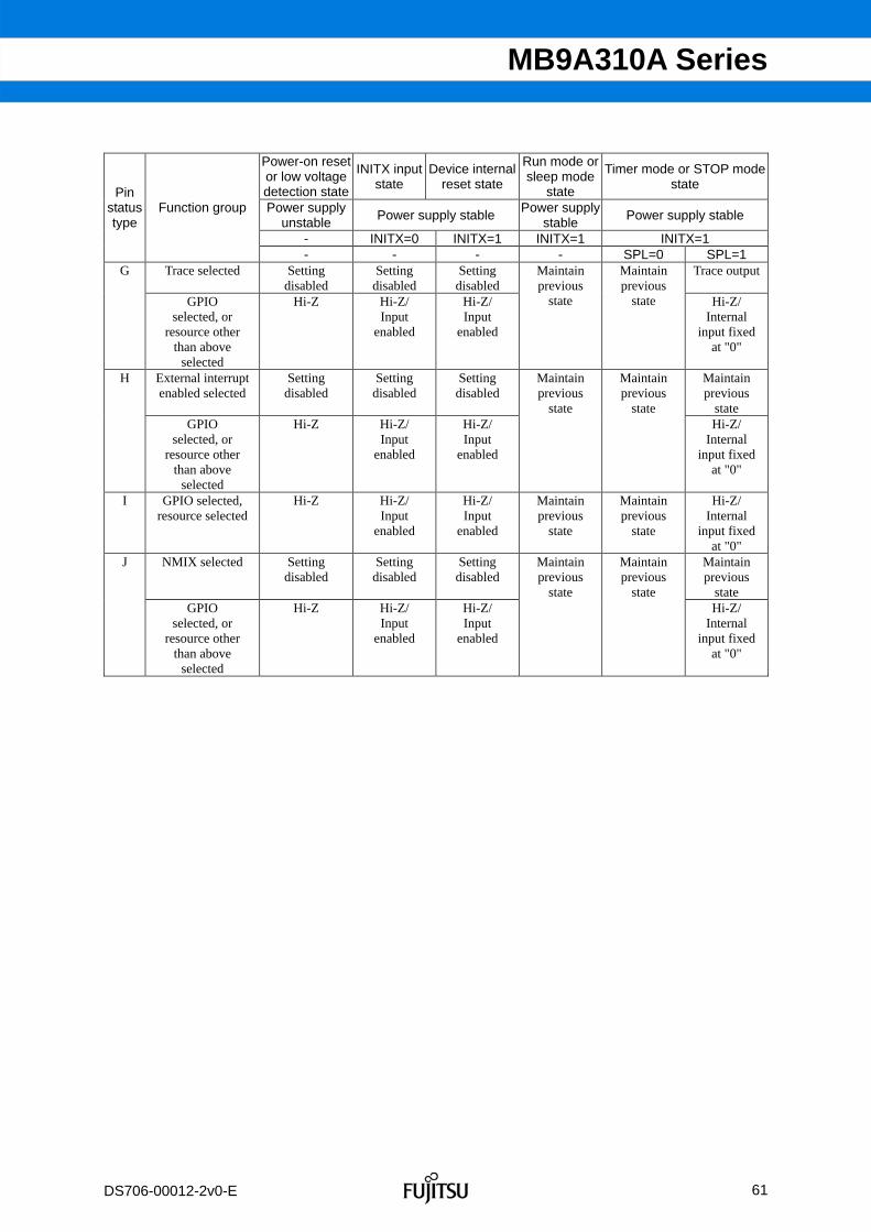
61
FUJITSU SEMICONDUCTOR CONFIDENTIAL r2.0
MB9A310A Series
DS706-00012-2v0-E
Power-on reset or low voltage detection state
INITX input state
Device internal reset state
Run mode or sleep mode
state
Timer mode or STOP mode state
Power supply unstable
Power supply stable Power supply
stable Power supply stable
- INITX=0 INITX=1 INITX=1 INITX=1
Pin status type
Function group
- - - - SPL=0 SPL=1 Trace selected Setting
disabled Setting disabled
Setting disabled
Trace outputG
GPIO selected, or
resource other than above
selected
Hi-Z Hi-Z/ Input
enabled
Hi-Z/ Input
enabled
Maintain previous
state
Maintain previous
state Hi-Z/ Internal
input fixed at "0"
External interrupt enabled selected
Setting disabled
Setting disabled
Setting disabled
Maintain previous
state
H
GPIO selected, or
resource other than above
selected
Hi-Z Hi-Z/ Input
enabled
Hi-Z/ Input
enabled
Maintain previous
state
Maintain previous
state Hi-Z/
Internal input fixed
at "0"
I GPIO selected, resource selected
Hi-Z Hi-Z/ Input
enabled
Hi-Z/ Input
enabled
Maintain previous
state
Maintain previous
state
Hi-Z/ Internal
input fixed at "0"
NMIX selected Setting disabled
Setting disabled
Setting disabled
Maintain previous
state
J
GPIO selected, or
resource other than above
selected
Hi-Z Hi-Z/ Input
enabled
Hi-Z/ Input
enabled
Maintain previous
state
Maintain previous
state Hi-Z/
Internal input fixed
at "0"

62
FUJITSU SEMICONDUCTOR CONFIDENTIAL r2.0
MB9A310A Series
DS706-00012-2v0-E
Power-on reset or low voltage detection state
INITX input state
Device internal reset state
Run mode or sleep mode
state
Timer mode or STOP mode state
Power supply unstable
Power supply stable Power supply
stable Power supply stable
- INITX=0 INITX=1 INITX=1 INITX=1
Pin status type
Function group
- - - - SPL=0 SPL=1 Analog input
selected Hi-Z Hi-Z/
Internal input fixed
at "0"/ Analog input
enabled
Hi-Z/ Internal
input fixed at "0"/ Analog input
enabled
Hi-Z/ Internal
input fixed at "0"/ Analog input
enabled
Hi-Z/ Internal
input fixed at "0"/ Analog input
enabled
Hi-Z/ Internal
input fixed at "0"/ Analog input
enabled
K
GPIO selected, or
resource other than above
selected
Setting disabled
Setting disabled
Setting disabled
Maintain previous
state
Maintain previous
state
Hi-Z/ Internal
input fixed at "0"
External interrupt enabled selected
Setting disabled
Setting disabled
Setting disabled
Maintain previous
state
Maintain previous
state
Maintain previous
state Analog input
selected Hi-Z Hi-Z/
Internal input fixed
at "0"/ Analog input
enabled
Hi-Z/ Internal
input fixed at "0"/ Analog input
enabled
Hi-Z/ Internal
input fixed at "0"/ Analog input
enabled
Hi-Z/ Internal
input fixed at "0"/ Analog input
enabled
Hi-Z/ Internal
input fixed at "0"/ Analog input
enabled
L
GPIO selected, or
resource other than above
selected
Setting disabled
Setting disabled
Setting disabled
Maintain previous
state
Maintain previous
state
Hi-Z/ Internal
input fixed at "0"
GPIO selected Setting disabled
Setting disabled
Setting disabled
Maintain previous
state
Maintain previous
state
Hi-Z/ Internal
input fixed at "0"
M
Sub crystal oscillator input
pin
Input enabled Input enabled
Input enabled
Input enabled
Input enabled
Input enabled

63
FUJITSU SEMICONDUCTOR CONFIDENTIAL r2.0
MB9A310A Series
DS706-00012-2v0-E
Power-on reset or low voltage detection state
INITX input state
Device internal reset state
Run mode or sleep mode
state
Timer mode or STOP mode state
Power supply unstable
Power supply stable Power supply
stable Power supply stable
- INITX=0 INITX=1 INITX=1 INITX=1
Pin status type
Function group
- - - - SPL=0 SPL=1 GPIO selected Setting
disabled Setting disabled
Setting disabled
Maintain previous
state
Maintain previous
state
Hi-Z/ Internal
input fixed at "0"
N
Sub crystal oscillator output
pin
Hi-Z/ Internal input fixed at "0"/
or Input enabled
Hi-Z/ Internal
input fixed at "0"
Hi-Z/ Internal
input fixed at "0"
Maintain previous
state
Maintain previous
state/ Hi-Z at
oscillation stop*2/ Internal
input fixed at "0"
Maintain previous
state/ Hi-Z at
oscillation stop*2/ Internal
input fixed at "0"
GPIO selected Hi-Z Hi-Z/ Input
enabled
Hi-Z/ Input
enabled
Maintain previous
state
Maintain previous
state
Hi-Z/ Internal
input fixed at "0"
O
USB I/O pin Setting disabled
Setting disabled
Setting disabled
Maintain previous
state
Hi-Z at transmission
/ Input enabled/ Internal
input fixed at "0" at reception
Hi-Z at transmission
/ Input enabled/ Internal
input fixed at "0" at reception
Mode input pin Input enabled Input enabled
Input enabled
Input enabled
Input enabled
Input enabled
P
GPIO selected Setting disabled
Setting disabled
Setting disabled
Maintain previous
state
Maintain previous
state
Hi-Z/Input enabled
*1 : Oscillation is stopped at sub timer mode, low speed CR timer mode, and stop mode. *2 : Oscillation is stopped at stop mode.

64
FUJITSU SEMICONDUCTOR CONFIDENTIAL r2.1
MB9A310A Series
DS706-00012-2v0-E
ELECTRICAL CHARACTERISTICS 1. Absolute Maximum Ratings
Rating
Parameter SymbolMin Max
Unit Remarks
Power supply voltage*1, *2 Vcc Vss - 0.5 Vss + 6.5 V Power supply voltage (for USB) *1, *3 USBVcc Vss - 0.5 Vss + 6.5 V Analog power supply voltage*1, *4 AVcc Vss - 0.5 Vss + 6.5 V Analog reference voltage*1, *4 AVRH Vss - 0.5 Vss + 6.5 V
Vss - 0.5 Vcc + 0.5 (≤ 6.5V)
V Except for USB pin
Vss - 0.5 USBVcc + 0.5
(≤ 6.5V) V USB pin
Input voltage*1 VI
Vss - 0.5 Vss + 6.5 V 5V tolerant
Analog pin input voltage*1 VIA Vss - 0.5 AVcc + 0.5
(≤ 6.5V) V
Output voltage*1 VO Vss - 0.5 Vcc + 0.5 (≤ 6.5V)
V
10 mA 4mA type "L" level maximum output current*5 IOL -
20 mA 12mA type 4 mA 4mA type
"L" level average output current*6 IOLAV - 12 mA 12mA type
"L" level total maximum output current ∑IOL - 100 mA "L" level total average output current*7 ∑IOLAV - 50 mA
- 10 mA 4mA type "H" level maximum output current*5 IOH -
- 20 mA 12mA type - 4 mA 4mA type
"H" level average output current*6 IOHAV - - 12 mA 12mA type
"H" level total maximum output current ∑IOH - - 100 mA "H" level total average output current*7 ∑IOHAV - - 50 mA Power consumption PD - 300 mW Storage temperature TSTG - 55 + 150 °C
*1 : These parameters are based on the condition that Vss = AVss = 0.0V. *2 : Vcc must not drop below Vss - 0.5V. *3 : USBVcc must not drop below Vss - 0.5V. *4 : Be careful not to exceed Vcc + 0.5 V, for example, when the power is turned on. *5 : The maximum output current is defined as the value of the peak current flowing through any one of the
corresponding pins. *6 : The average output current is defined as the average current value flowing through any one of the
corresponding pins for a 100 ms period. *7 : The total average output current is defined as the average current value flowing through all of
corresponding pins for a 100ms. <WARNING>
Semiconductor devices can be permanently damaged by application of stress (voltage, current, temperature, etc.) in excess of absolute maximum ratings. Do not exceed these ratings.

65
FUJITSU SEMICONDUCTOR CONFIDENTIAL r2.1
MB9A310A Series
DS706-00012-2v0-E
2. Recommended Operating Conditions (Vss = AVss = 0.0V)
Value Parameter Symbol Conditions
Min Max Unit Remarks
Power supply voltage Vcc - 2.7 5.5 V
3.0 3.6
(≤ Vcc)*1
Power supply voltage (3V power supply) for USB
USBVcc 2.7
5.5 (≤ Vcc)
V *2
Analog power supply voltage AVcc - 2.7 5.5 V AVcc = Vcc Analog reference voltage AVRH - AVss AVcc V
FPT-100P-M20 FPT-100P-M23 FPT-80P-M21 FPT-80P-M37 FPT-64P-M24 FPT-64P-M38 FPT-64P-M23 FPT-64P-M39 LCC-64P-M24 BGA-112P-M04
Ta - - 40 + 105 °C
When mounted on four-layer
PCB
- 40 + 105 °C
- 40 + 105 °C Icc ≤ 35mA
Operating temperature
FPT-100P-M06 Ta When mounted on double-sided single-layer
PCB
- 40 + 85 °C Icc > 35mA
*1: When P81/UDP0 and P80/UDM0 pin are used as USB (UDP0, UDM0). *2: When P81/UDP0 and P80/UDM0 pin are used as GPIO (P81, P80). <WARNING>
The recommended operating conditions are required in order to ensure the normal operation of the semiconductor device. All of the device's electrical characteristics are warranted when the device is operated within these ranges. Always use semiconductor devices within their recommended operating condition ranges. Operation outside these ranges may adversely affect reliability and could result in device failure. No warranty is made with respect to uses, operating conditions, or combinations not represented on the data sheet. Users considering application outside the listed conditions are advised to contact their representatives beforehand.

66
FUJITSU SEMICONDUCTOR CONFIDENTIAL r2.1
MB9A310A Series
DS706-00012-2v0-E
3. DC Characteristics Current rating
(Vcc = AVcc = 2.7V to 5.5V, USBVcc = 3.0V to 3.6V, Vss = AVss = 0V, Ta = - 40°C to + 105°C) Value
Parameter SymbolPin
name Conditions
Min Typ MaxUnit Remarks
- 32 41 mA
CPU : 40MHz, Peripheral : 40MHz, Flash 0Wait FRWTR.RWT = 00 FSYNDN.SD = 000 *1
Normal operation(PLL)
Vcc = 5.5V
- 21 28 mA
CPU : 40MHz, Peripheral : 40MHz, Flash 3Wait FRWTR.RWT = 00 FSYNDN.SD = 011 *1
Normal operation(built-in
high-speed CR)Vcc = 5.5V
- 3.9 7.7 mA
CPU/ Peripheral : 4MHz *1, *2 Flash 0Wait FRWTR.RWT = 00 FSYNDN.SD = 000
Normal operation(sub oscillation)
Vcc = 5.5V - 0.15 3.2 mA
CPU/ Peripheral : 32kHz Flash 0Wait FRWTR.RWT = 00 FSYNDN.SD = 000 *1
Icc
Normal operation(built-in
low-speed CR)Vcc = 5.5V
- 0.2 3.3 mA
CPU/ Peripheral : 100kHz Flash 0Wait FRWTR.RWT = 00 FSYNDN.SD = 000 *1
SLEEP operation(PLL)
Vcc = 5.5V - 10 15 mA
Peripheral : 40MHz *1
SLEEP operation(built-in
high-speed CR)Vcc = 5.5V
- 1.2 4.4 mAPeripheral : 4MHz *1, *2
SLEEP operation(sub oscillation)
Vcc = 5.5V - 0.1 3.1 mA
Peripheral : 32kHz *1
Power supply current
Iccs
Vcc
SLEEP operation(built in
low-speed CR)Vcc = 5.5V
- 0.1 3.1 mAPeripheral : 100kHz *1

67
FUJITSU SEMICONDUCTOR CONFIDENTIAL r2.1
MB9A310A Series
DS706-00012-2v0-E
Value Parameter Symbol
Pin name
Conditions Min Typ Max
Unit Remarks
- 35 200 μA Ta = + 25°C, When LVD is off *1
ICCH STOP mode Vcc = 5.5V
- - 3 mA Ta = + 105°C, When LVD is off *1
- 60 230 μA Ta = + 25°C, When LVD is off *1
Power supply current
ICCT TIMER mode
(sub oscillation)Vcc = 5.5V
- - 3.1 mA Ta = + 105°C, When LVD is off *1
Low-voltage detection circuit (LVD) power supply current
ICCLVD
Vcc
At operation Vcc = 5.5V
- 4 7 μA For occurrence of interrupt
*1: When all ports are fixed. *2: When setting it to 4MHz by trimming.
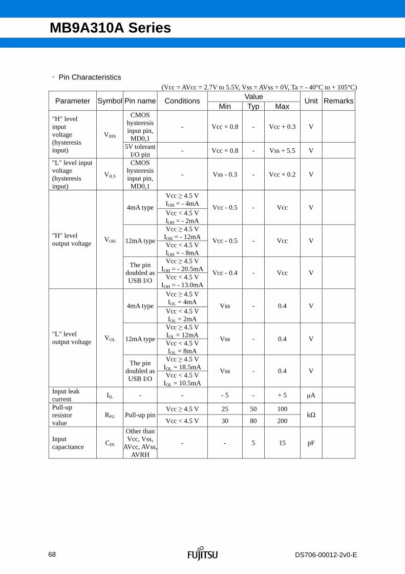
68
FUJITSU SEMICONDUCTOR CONFIDENTIAL r2.1
MB9A310A Series
DS706-00012-2v0-E
Pin Characteristics (Vcc = AVcc = 2.7V to 5.5V, Vss = AVss = 0V, Ta = - 40°C to + 105°C)
Value Parameter Symbol Pin name Conditions
Min Typ Max Unit Remarks
CMOS hysteresis input pin, MD0,1
- Vcc × 0.8 - Vcc + 0.3 V "H" level input voltage (hysteresis input)
VIHS
5V tolerant I/O pin
- Vcc × 0.8 - Vss + 5.5 V
"L" level input voltage (hysteresis input)
VILS
CMOS hysteresis input pin, MD0,1
- Vss - 0.3 - Vcc × 0.2 V
Vcc ≥ 4.5 V IOH = - 4mA
4mA type Vcc < 4.5 V IOH = - 2mA
Vcc - 0.5 - Vcc V
Vcc ≥ 4.5 V IOH = - 12mA
12mA type Vcc < 4.5 V IOH = - 8mA
Vcc - 0.5 - Vcc V
Vcc ≥ 4.5 V IOH = - 20.5mA
"H" level output voltage
VOH
The pin doubled as USB I/O Vcc < 4.5 V
IOH = - 13.0mA
Vcc - 0.4 - Vcc V
Vcc ≥ 4.5 V IOL = 4mA
4mA type Vcc < 4.5 V IOL = 2mA
Vss - 0.4 V
Vcc ≥ 4.5 V IOL = 12mA
12mA type Vcc < 4.5 V IOL = 8mA
Vss - 0.4 V
Vcc ≥ 4.5 V IOL = 18.5mA
"L" level output voltage
VOL
The pin doubled as USB I/O Vcc < 4.5 V
IOL = 10.5mA
Vss - 0.4 V
Input leak current
IIL - - - 5 - + 5 μA
Vcc ≥ 4.5 V 25 50 100 Pull-up resistor value
RPU Pull-up pin Vcc < 4.5 V 30 80 200
kΩ
Input capacitance
CIN
Other than Vcc, Vss,
AVcc, AVss,AVRH
- - 5 15 pF
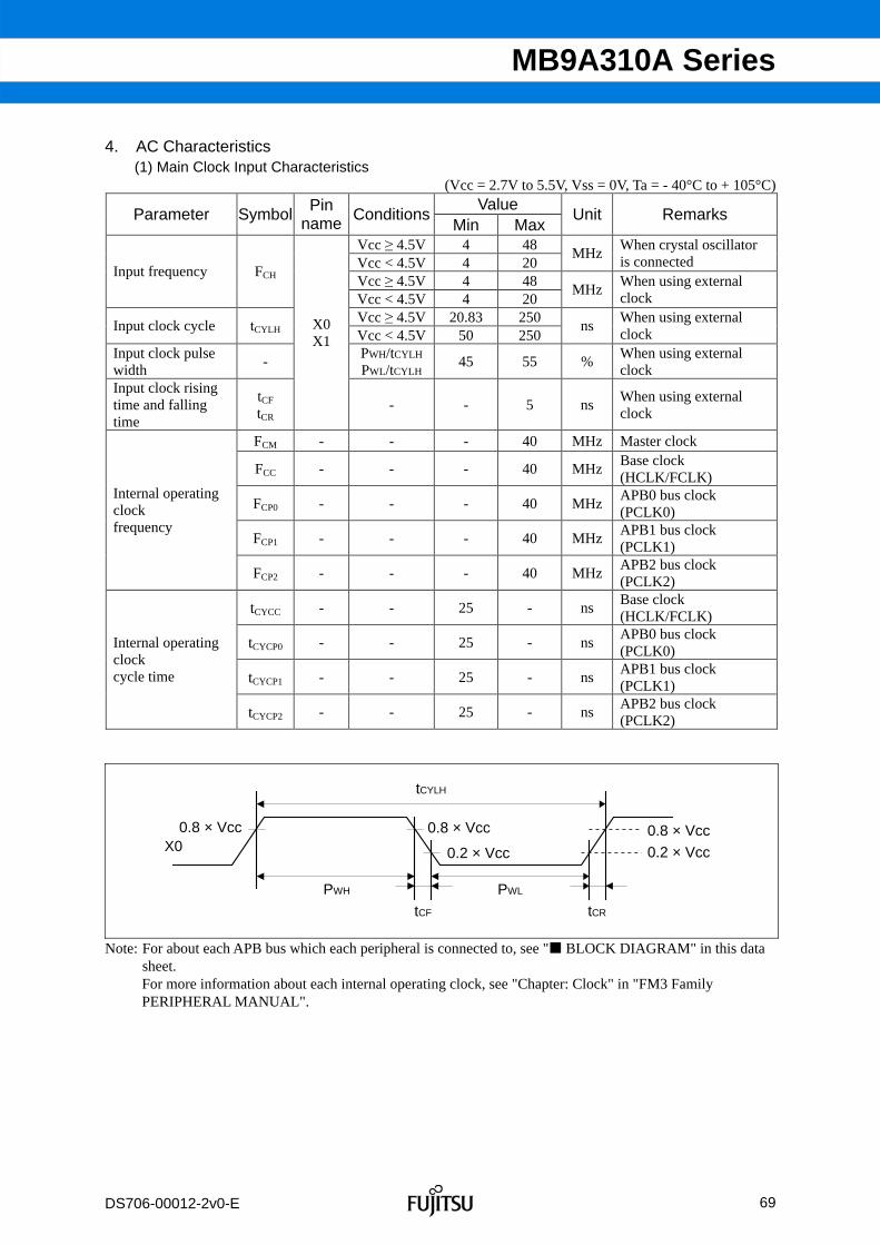
69
FUJITSU SEMICONDUCTOR CONFIDENTIAL r2.1
MB9A310A Series
DS706-00012-2v0-E
4. AC Characteristics (1) Main Clock Input Characteristics
(Vcc = 2.7V to 5.5V, Vss = 0V, Ta = - 40°C to + 105°C) Value
Parameter Symbol Pin
name Conditions
Min Max Unit Remarks
Vcc ≥ 4.5V 4 48 Vcc < 4.5V 4 20
MHzWhen crystal oscillator is connected
Vcc ≥ 4.5V 4 48 Input frequency FCH
Vcc < 4.5V 4 20 MHz
When using external clock
Vcc ≥ 4.5V 20.83 250 Input clock cycle tCYLH
Vcc < 4.5V 50 250 ns
When using external clock
Input clock pulse width
- PWH/tCYLH
PWL/tCYLH45 55 %
When using external clock
Input clock rising time and falling time
tCF
tCR
X0 X1
- - 5 ns When using external clock
FCM - - - 40 MHz Master clock
FCC - - - 40 MHzBase clock (HCLK/FCLK)
FCP0 - - - 40 MHzAPB0 bus clock (PCLK0)
FCP1 - - - 40 MHzAPB1 bus clock (PCLK1)
Internal operating clock frequency
FCP2 - - - 40 MHzAPB2 bus clock (PCLK2)
tCYCC - - 25 - ns Base clock (HCLK/FCLK)
tCYCP0 - - 25 - ns APB0 bus clock (PCLK0)
tCYCP1 - - 25 - ns APB1 bus clock (PCLK1)
Internal operating clock cycle time
tCYCP2 - - 25 - ns APB2 bus clock (PCLK2)
0.8 × Vcc
tCYLH
0.8 × Vcc
0.2 × Vcc 0.2 × Vcc
0.8 × Vcc
PWLPWH
tCF tCR
Note: For about each APB bus which each peripheral is connected to, see " BLOCK DIAGRAM" in this data sheet.
For more information about each internal operating clock, see "Chapter: Clock" in "FM3 Family PERIPHERAL MANUAL".
X0

70
FUJITSU SEMICONDUCTOR CONFIDENTIAL r2.1
MB9A310A Series
DS706-00012-2v0-E
(2) Sub Clock Input Characteristics (Vcc = 2.7V to 5.5V, Vss = 0V, Ta = - 40°C to + 105°C)
Value Parameter Symbol
Pin name
ConditionsMin Typ Max
Unit Remarks
- - 32.768 - kHz When crystal oscillator is connected Input frequency FCL
- 32 - 100 kHz When using external clock
Input clock cycle tCYLL - 10 - 31.25 μs When using external clock
Input clock pulse width
-
X0A X1A
PWH/tCYLL
PWL/tCYLL45 - 55 %
When using external clock
0.8 × Vcc
tCYLL
0.8 × Vcc
0.2 × Vcc 0.2 × Vcc
0.8 × Vcc
PWLPWH
(3) Built-in CR Oscillation Characteristics
Built-in high-speed CR
(Vcc = 2.7V to 5.5V, Vss = 0V, Ta = - 40°C to + 105°C) Value
Parameter Symbol Conditions Min Typ Max
Unit Remarks
Ta = + 25°C 3.96 4 4.04
Ta = 0°C to + 70°C
3.84 4 4.16
Ta = - 40°C to + 105°C
3.8 4 4.2
When trimming* Clock frequency FCRH
Ta = - 40°C to + 105°C
3 4 5
MHz
When not trimming
*: In the case of using the values in CR trimming area of Flash memory at shipment for frequency trimming.
Built-in low-speed CR
(Vcc = 2.7V to 5.5V, Vss = 0V, Ta = - 40°C to + 105°C) Value
Parameter Symbol Conditions Min Typ Max
Unit Remarks
Clock frequency FCRL - 50 100 150 kHz
X0A

71
FUJITSU SEMICONDUCTOR CONFIDENTIAL r2.1
MB9A310A Series
DS706-00012-2v0-E
(4-1) Operating Conditions of Main and USB PLL (In the case of using main clock for input clock
of PLL) (Vcc = 2.7V to 5.5V, Vss = 0V, Ta = - 40°C to + 105°C)
Value Parameter Symbol
Min Typ MaxUnit Remarks
PLL oscillation stabilization wait time (LOCK UP time)*
tLOCK 100 - - μs
PLL input clock frequency fPLLI 4 - 16 MHz PLL multiple rate - 13 - 75 multiple PLL macro oscillation clock frequency fPLLO 200 - 300 MHz
*: Time from when the PLL starts operating until the oscillation stabilizes.
(4-2) Operating Conditions of Main PLL (In the case of using the built-in high speed CR for the
input clock of the main PLL) (Vcc = 2.7V to 5.5V, Vss = 0V, Ta = - 40°C to + 105°C)
Value Parameter Symbol
Min Typ MaxUnit Remarks
PLL oscillation stabilization wait time (LOCK UP time)*
tLOCK 100 - - μs
PLL input clock frequency fPLLI 3.8 4 4.2 MHz PLL multiple rate - 50 - 71 multiple PLL macro oscillation clock frequency fPLLO 190 - 300 MHz
*: Time from when the PLL starts operating until the oscillation stabilizes. Note: Make sure to input the built-in high-speed CR clock that has been trimmed.
When setting PLL multiple rate, please take the accuracy of the built-in high-speed CR clock into account and prevent the master clock from exceeding the maximum frequency.
(5) Reset Input Characteristics
(Vcc = 2.7V to 5.5V, Vss = 0V, Ta = - 40°C to + 105°C)
Value Parameter Symbol
Pin name
ConditionsMin Max
Unit Remarks
Reset input time tINITX INITX - 500 - ns
(6) Power-on Reset Timing
(Vcc = 2.7V to 5.5V, Vss = 0V, Ta = - 40°C to + 105°C)
Value Parameter Symbol
Pin name Min Max
Unit Remarks
Power supply rising time Tr 0 - ms
Power supply shut down time Toff Vcc
1 - ms
0.2V
2.7V
Tr
Vcc
Toff
0.2V 0.2V

72
FUJITSU SEMICONDUCTOR CONFIDENTIAL r2.1
MB9A310A Series
DS706-00012-2v0-E
(7) External Bus Timing
External bus clock output Characteristics
(Vcc = 2.7V to 5.5V, Vss = 0V, Ta = - 40°C to + 105°C) Value
Parameter Symbol Pin name Conditions Min Max
Unit
Vcc ≥ 4.5 V - 40 MHz Output frequency tCYCLE
Vcc < 4.5 V - 32 MHz Vcc ≥ 4.5 V 25 - ns Minimum clock cycle
time -
MCLKOUT
Vcc < 4.5 V 31.25 - ns Note: The external bus clock output is a divided clock of HCLK. For more information about setting of clock
divider, see "Chapter: External Bus Interface" in "FM3 Family PERIPHERAL MANUAL" When external bus clock is not output, this characteristics does not give any effect on external bus
operation.
0.8 × Vcc
tCYCLE
0.8 × Vcc
0.2 × Vcc 0.2 × Vcc
0.8 × Vcc
PWLPWH
External bus signal input/output Characteristics
(Vcc = 2.7V to 5.5V, Vss = 0V, Ta = - 40°C to + 105°C)
Parameter Symbol Conditions Value Unit Remarks
VIH 0.8 × VCC V Signal input characteristics
VIL 0.2 × VCC V
VOH 0.8 × VCC V Signal output characteristics
VOL
-
0.2 × VCC V
VIH
VIL VIL
VIH
VOH
VOL VOL
VOH
MCLKOUT
Input signal
Output signal

73
FUJITSU SEMICONDUCTOR CONFIDENTIAL r2.1
MB9A310A Series
DS706-00012-2v0-E
Separate Bus Access Asynchronous SRAM Mode
(Vcc = 2.7V to 5.5V, Vss = 0V, Ta = - 40°C to + 105°C) Value
Parameter Symbol Pin name ConditionsMin Max
Unit
Vcc ≥ 4.5V MOEX Min pulse width
tOEW MOEX Vcc < 4.5V
MCLK×n-3 - ns
Vcc ≥ 4.5V -9 + 9 MCSX ↓→ Address output delay time
tCSL – AV MCSX[7:0] MAD[24:0] Vcc < 4.5V -12 + 12
ns
Vcc ≥ 4.5V MCLK×m+9MOEX ↑ → Address hold time
tOEH - AX MOEX
MAD[24:0] Vcc < 4.5V 0
MCLK×m+12ns
Vcc ≥ 4.5V MCLK×m-9 MCLK×m+9MCSX ↓→ MOEX ↓ delay time
tCSL - OEL Vcc < 4.5V MCLK×m-12 MCLK×m+12
ns
Vcc ≥ 4.5V MCLK×m+9MOEX ↑ → MCSX ↑ time
tOEH - CSH
MOEX MCSX[7:0]
Vcc < 4.5V 0
MCLK×m+12ns
Vcc ≥ 4.5V MCLK×m-9 MCLK×m+9MCSX ↓ → MDQM ↓ delay time
tCSL - RDQML MCSX
MDQM[1:0] Vcc < 4.5V MCLK×m-12 MCLK×m+12ns
Vcc ≥ 4.5V 20 - Data set up → MOEX ↑ time
tDS - OE MOEX
MADATA[15:0] Vcc < 4.5V 38 - ns
Vcc ≥ 4.5V MOEX ↑ → Data hold time
tDH - OE MOEX
MADATA[15:0] Vcc < 4.5V 0 - ns
Vcc ≥ 4.5V MWEX Min pulse width
tWEW MWEX Vcc < 4.5V
MCLK×n-3 - ns
Vcc ≥ 4.5V MCLK×m+9MWEX ↑ → Address output delay time
tWEH - AX MWEX
MAD[24:0] Vcc < 4.5V 0
MCLK×m+12ns
Vcc ≥ 4.5V MCLK×n-9 MCLK×n+9MCSX ↓ → MWEX ↓ delay time
tCSL - WEL Vcc < 4.5V MCLK×n-12 MCLK×n+12
ns
Vcc ≥ 4.5V MCLK×m+9MWEX ↑ → MCSX ↑ delay time
tWEH - CSH
MWEX MCSX[7:0]
Vcc < 4.5V 0
MCLK×m+12ns
Vcc ≥ 4.5V MCLK×n-9 MCLK×n+9MCSX ↓ → MDQM ↓ delay time
tCSL-WDQML MCSX
MDQM[1:0] Vcc < 4.5V MCLK×n-12 MCLK×n+12ns
Vcc ≥ 4.5V - 9 + 9 MWEX ↓ → Data output time
tWEL - DV Vcc < 4.5V -12 + 12
ns
Vcc ≥ 4.5V MCLK×m+9MWEX ↑ → Data hold time
tWEH - DX
MWEX MADATA[15:0]
Vcc < 4.5V 0
MCLK×m+12ns
Note: When the external load capacitance CL = 30pF (m = 0 to 15, n = 1 to 16).

74
FUJITSU SEMICONDUCTOR CONFIDENTIAL r2.1
MB9A310A Series
DS706-00012-2v0-E
Address
RD WD
Address
tCYCLE
tOEH - CSH
tOEH - AX tCSL - AV tWEH - AX
tWEH - CSH
tCSL - AV
tCSL - OEL
tOEW
tDS - OE tDH - OE tWEL -DV
tWEW
tCSL -WEL
tCSL -WDQML
tWEH -DX
tCSL - RDQML
MCLK
MCSX[7:0]
MAD[24:0]
MDQM[1:0]
MWEX
MADATA[15:0]
MOEX

75
FUJITSU SEMICONDUCTOR CONFIDENTIAL r2.1
MB9A310A Series
DS706-00012-2v0-E
Separate Bus Access Synchronous SRAM Mode
(Vcc = 2.7V to 5.5V, Vss = 0V, Ta = - 40°C to + 105°C) Value
Parameter Symbol Pin name ConditionsMin Max
Unit
Vcc ≥ 4.5V 9 Address delay time tAV
MCLK MAD[24:0] Vcc < 4.5V
1 12
ns
Vcc ≥ 4.5V 9 tCSL
Vcc < 4.5V1
12 ns
Vcc ≥ 4.5V 9 MCSX delay time
tCSH
MCLK MCSX[7:0]
Vcc < 4.5V1
12 ns
Vcc ≥ 4.5V 9 tREL
Vcc < 4.5V1
12 ns
Vcc ≥ 4.5V 9 MOEX delay time
tREH
MCLK MOEX
Vcc < 4.5V1
12 ns
Vcc ≥ 4.5V 19 Data set up → MCLK ↑ time
tDS MCLK
MADATA[15:0] Vcc < 4.5V 37 - ns
Vcc ≥ 4.5V MCLK ↑→ Data hold time
tDH MCLK
MADATA[15:0] Vcc < 4.5V0 - ns
Vcc ≥ 4.5V 9 tWEL
Vcc < 4.5V1
12 ns
Vcc ≥ 4.5V 9 MWEX delay time
tWEH
MCLK MWEX
Vcc < 4.5V1
12 ns
Vcc ≥ 4.5V 9 tDQML
Vcc < 4.5V1
12 ns
Vcc ≥ 4.5V 9 MDQM[1:0] delay time
tDQMH
MCLK MDQM[1:0]
Vcc < 4.5V1
12 ns
Vcc ≥ 4.5V 1 18 MCLK ↑ → Data output time
tOD MCLK
MADATA[15:0] Vcc < 4.5V 1 24 ns
Note: When the external load capacitance CL = 30pF.
tCYCLE
AddressAddress
RD WD
tCSL
tAV
tREL
tDQML
tREH
tAV
tCSH
tDQMH
tDS tDH tOD tOD
tWEL tWEH
tDQML tDQMH
MCLK
MCSX[7:0]
MAD[24:0]
MDQM[1:0]
MWEX
MADATA[15:0]
MOEX

76
FUJITSU SEMICONDUCTOR CONFIDENTIAL r2.1
MB9A310A Series
DS706-00012-2v0-E
Multiplexed Bus Access Asynchronous SRAM Mode
(Vcc = 2.7V to 5.5V, Vss = 0V, Ta = - 40°C to + 105°C) Value
Parameter Symbol Pin name ConditionsMin Max
Unit
Vcc ≥ 4.5V 10 Multiplexed Address delay time
tALE-CHMADV Vcc < 4.5V
0 20
ns
Vcc ≥ 4.5V MCLK×n+0 MCLK×n+10Multiplexed Address hold time
tCHMADH
MALE MADATA[15:0]
Vcc < 4.5V MCLK×n+0 MCLK×n+20ns
Note: When the external load capacitance CL = 30pF (m = 0 to 15, n = 1 to 16).
AddressAddress
RD
tCHMADHtALE - CHMADVtALE - CHMADV
tCYCLE
Address Address WD
MCLK
MCSX[7:0]
MALE
MOEX
MWEX
MADATA[15:0]
MAD [24:0]
MDQM [1:0]

77
FUJITSU SEMICONDUCTOR CONFIDENTIAL r2.1
MB9A310A Series
DS706-00012-2v0-E
Multiplexed Bus Access Synchronous SRAM Mode
(Vcc = 2.7V to 5.5V, Vss = 0V, Ta = - 40°C to + 105°C) Value
Parameter Symbol Pin name ConditionsMin Max
Unit Remarks
Vcc ≥ 4.5V 9 ns tCHAL
Vcc < 4.5V1
12 ns Vcc ≥ 4.5V 9 ns
MALE delay time tCHAH
MCLK ALE
Vcc < 4.5V1
12 ns
Vcc ≥ 4.5VMCLK ↑ → Multiplexed Address delay time
tCHMADV Vcc < 4.5V
1 tOD ns
Vcc ≥ 4.5VMCLK ↑ → Multiplexed Data output time
tCHMADX
MCLK MADATA[15:0]
Vcc < 4.5V1 tOD ns
Note: When the external load capacitance CL = 30pF.
Address
Address AddressRD WD
Address
tCYCLE
tCHAH tCHAL
tCHMADXtCHMADVtCHMADV
MCLK
MCSX[7:0]
MALE
MOEX
MWEX
MADATA[15:0]
MAD [24:0]
MDQM [1:0]

78
FUJITSU SEMICONDUCTOR CONFIDENTIAL r2.1
MB9A310A Series
DS706-00012-2v0-E
External Ready Input Timing
(Vcc = 2.7V to 5.5V, Vss = 0V, Ta = - 40°C to + 105°C) Value
Parameter Symbol Pin name ConditionsMin Max
Unit Remarks
Vcc ≥ 4.5V 19 MCLK ↑ MRDY input setup time
tRDYI MCLK MRDY Vcc < 4.5V 37
- ns
When RDY is input
· · ·
Over 2cycles
tRDYI
When RDY is released
· · · · · ·
2 cycles
tRDYI
0.5×VCC
MCLK
Original MOEX MWEX
MRDY
MCLK
Extended MOEX MWEX
MRDY
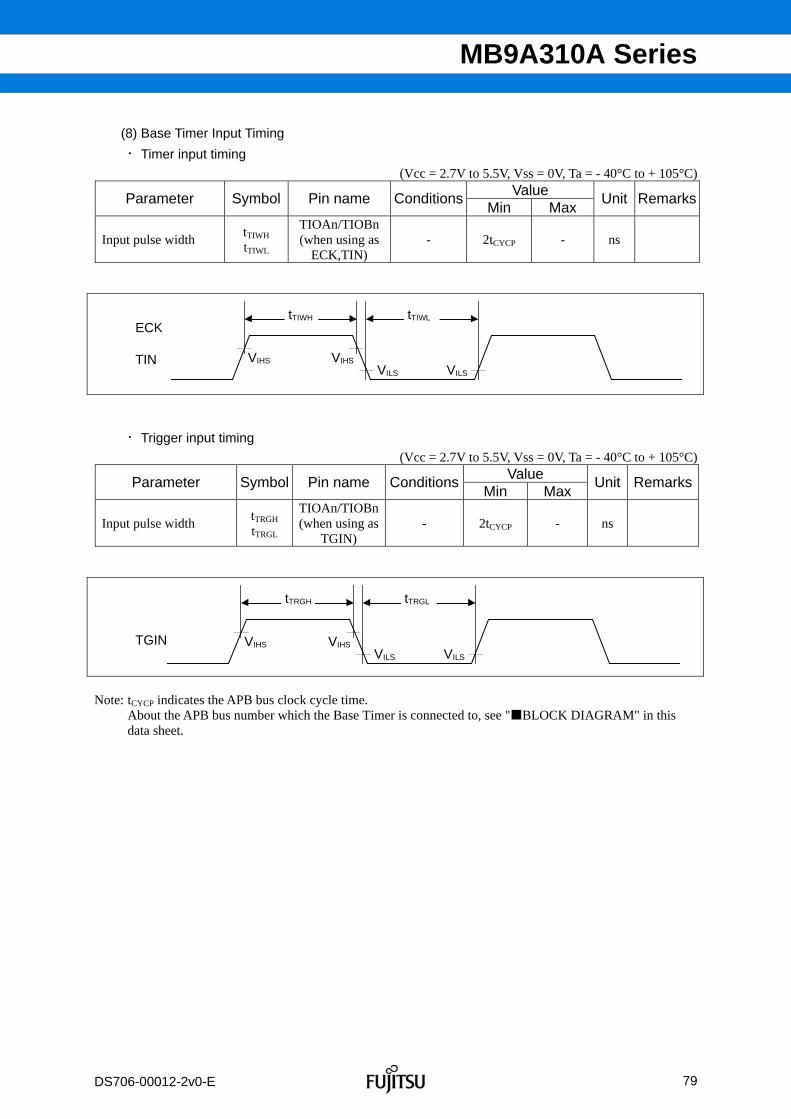
79
FUJITSU SEMICONDUCTOR CONFIDENTIAL r2.1
MB9A310A Series
DS706-00012-2v0-E
(8) Base Timer Input Timing
Timer input timing
(Vcc = 2.7V to 5.5V, Vss = 0V, Ta = - 40°C to + 105°C) Value
Parameter Symbol Pin name ConditionsMin Max
Unit Remarks
Input pulse width tTIWH tTIWL
TIOAn/TIOBn(when using as
ECK,TIN) - 2tCYCP - ns
tTIWH
VIHS VIHSVILS VILS
tTIWL
Trigger input timing
(Vcc = 2.7V to 5.5V, Vss = 0V, Ta = - 40°C to + 105°C) Value
Parameter Symbol Pin name ConditionsMin Max
Unit Remarks
Input pulse width tTRGH tTRGL
TIOAn/TIOBn(when using as
TGIN) - 2tCYCP - ns
tTRGH
VIHS VIHSVILS VILS
tTRGL
Note: tCYCP indicates the APB bus clock cycle time.
About the APB bus number which the Base Timer is connected to, see "BLOCK DIAGRAM" in this data sheet.
TGIN
ECK TIN

80
FUJITSU SEMICONDUCTOR CONFIDENTIAL r2.1
MB9A310A Series
DS706-00012-2v0-E
(9) UART Timing
Synchronous serial (SPI = 0, SCINV = 0)
(Vcc = 2.7V to 5.5V, Vss = 0V, Ta = - 40°C to + 105°C) Vcc < 4.5V Vcc ≥ 4.5V
Parameter Symbol Pin
nameConditions
Min Max Min Max Unit
Serial clock cycle time tSCYC SCKx 4tcycp - 4tcycp - ns
SCK ↓ → SOT delay time tSLOVI SCKxSOTx
- 30 + 30 - 20 + 20 ns
SIN → SCK ↑ setup time tIVSHI SCKxSINx
50 - 30 - ns
SCK ↑ → SIN hold time tSHIXI SCKxSINx
Internal shiftclock
operation
0 - 0 - ns
Serial clock "L" pulse width tSLSH SCKx2tcycp -
10 -
2tcycp - 10
- ns
Serial clock "H" pulse width tSHSL SCKxtcycp +
10 -
tcycp + 10
- ns
SCK ↓ → SOT delay time tSLOVE SCKxSOTx
- 50 - 30 ns
SIN → SCK ↑ setup time tIVSHE SCKxSINx
10 - 10 - ns
SCK ↑→ SIN hold time tSHIXE SCKxSINx
20 - 20 - ns
SCK falling time tF SCKx - 5 - 5 nsSCK rising time tR SCKx
External shiftclock
operation
- 5 - 5 ns
Notes: The above characteristics apply to CLK synchronous mode. tCYCP indicates the APB bus clock cycle time.
About the APB bus number which UART is connected to, see "BLOCK DIAGRAM" in this data sheet.
These characteristics only guarantee the same relocate port number. For example, the combination of SCLKx_0 and SOTx_1 is not guaranteed.
When the external load capacitance CL = 30pF.

81
FUJITSU SEMICONDUCTOR CONFIDENTIAL r2.1
MB9A310A Series
DS706-00012-2v0-E
tSCYC
VOH
VOH
VOL
VOL
VOL
VIH
VIL
VIH
VIL
tSLOVI
tIVSHI tSHIXI
MS bit = 0
tSLSH tSHSL
VIH
tF tR
VIH
VOH
VIHVIL VIL
VOL
VIH
VIL
VIH
VIL
tSLOVE
tIVSHE tSHIXE
MS bit = 1
SCK
SOT
SIN
SCK
SOT
SIN

82
FUJITSU SEMICONDUCTOR CONFIDENTIAL r2.1
MB9A310A Series
DS706-00012-2v0-E
Synchronous serial (SPI = 0, SCINV = 1)
(Vcc = 2.7V to 5.5V, Vss = 0V, Ta = - 40°C to + 105°C) Vcc < 4.5V Vcc ≥ 4.5V
Parameter Symbol Pin
nameConditions
Min Max Min Max Unit
Serial clock cycle time tSCYC SCKx 4tcycp - 4tcycp - ns
SCK ↑ → SOT delay time tSHOVI SCKxSOTx
- 30 + 30 - 20 + 20 ns
SIN → SCK ↓ setup time tIVSLI SCKxSINx
50 - 30 - ns
SCK ↓ → SIN hold time tSLIXI SCKxSINx
Internal shiftclock
operation
0 - 0 - ns
Serial clock "L" pulse width tSLSH SCKx2tcycp -
10 -
2tcycp - 10
- ns
Serial clock "H" pulse width tSHSL SCKxtcycp +
10 -
tcycp + 10
- ns
SCK ↑ → SOT delay time tSHOVE SCKxSOTx
- 50 - 30 ns
SIN → SCK ↓ setup time tIVSLE SCKxSINx
10 - 10 - ns
SCK ↓ → SIN hold time tSLIXE SCKxSINx
20 - 20 - ns
SCK falling time tF SCKx - 5 - 5 nsSCK rising time tR SCKx
External shiftclock
operation
- 5 - 5 ns
Notes: The above characteristics apply to CLK synchronous mode. tCYCP indicates the APB bus clock cycle time.
About the APB bus number which UART is connected to, see "BLOCK DIAGRAM" in this data sheet.
These characteristics only guarantee the same relocate port number. For example, the combination of SCLKx_0 and SOTx_1 is not guaranteed.
When the external load capacitance CL = 30pF.

83
FUJITSU SEMICONDUCTOR CONFIDENTIAL r2.1
MB9A310A Series
DS706-00012-2v0-E
tSCYC
VOH VOH
VOH
VOL
VOL
VIH
VIL
VIH
VIL
tSHOVI
tIVSLI tSLIXI
MS bit = 0
tSHSL tSLSH
VIH
tFtR
VIH
VOH
VILVIL VIL
VOL
VIH
VIL
VIH
VIL
tSHOVE
tIVSLE tSLIXE
MS bit = 1
SCK
SOT
SIN
SCK
SOT
SIN
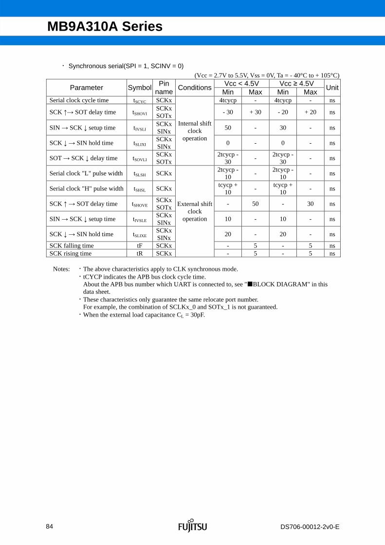
84
FUJITSU SEMICONDUCTOR CONFIDENTIAL r2.1
MB9A310A Series
DS706-00012-2v0-E
Synchronous serial(SPI = 1, SCINV = 0)
(Vcc = 2.7V to 5.5V, Vss = 0V, Ta = - 40°C to + 105°C) Vcc < 4.5V Vcc ≥ 4.5V
Parameter Symbol Pin
nameConditions
Min Max Min Max Unit
Serial clock cycle time tSCYC SCKx 4tcycp - 4tcycp - ns
SCK ↑→ SOT delay time tSHOVI SCKxSOTx
- 30 + 30 - 20 + 20 ns
SIN → SCK ↓ setup time tIVSLI SCKxSINx
50 - 30 - ns
SCK ↓ → SIN hold time tSLIXI SCKxSINx
0 - 0 - ns
SOT → SCK ↓ delay time tSOVLI SCKxSOTx
Internal shiftclock
operation
2tcycp - 30
- 2tcycp -
30 - ns
Serial clock "L" pulse width tSLSH SCKx2tcycp -
10 -
2tcycp - 10
- ns
Serial clock "H" pulse width tSHSL SCKxtcycp +
10 -
tcycp + 10
- ns
SCK ↑ → SOT delay time tSHOVE SCKxSOTx
- 50 - 30 ns
SIN → SCK ↓ setup time tIVSLE SCKxSINx
10 - 10 - ns
SCK ↓ → SIN hold time tSLIXE SCKxSINx
20 - 20 - ns
SCK falling time tF SCKx - 5 - 5 nsSCK rising time tR SCKx
External shiftclock
operation
- 5 - 5 ns
Notes: The above characteristics apply to CLK synchronous mode. tCYCP indicates the APB bus clock cycle time.
About the APB bus number which UART is connected to, see "BLOCK DIAGRAM" in this data sheet.
These characteristics only guarantee the same relocate port number. For example, the combination of SCLKx_0 and SOTx_1 is not guaranteed.
When the external load capacitance CL = 30pF.

85
FUJITSU SEMICONDUCTOR CONFIDENTIAL r2.1
MB9A310A Series
DS706-00012-2v0-E
tSOVLI
tSCYC
tSHOVIVOL VOL
VOH
VOH
VOL
VOH
VOL
VIH
VIL
VIH
VIL
tIVSLI tSLIXI
MS bit = 0
tF tR
tSLSH tSHSL
tSHOVE
VIL VILVIH VIH VIH
VOH
*VOL
VOH
VOL
VIH
VIL
VIH
VIL
tIVSLE tSLIXE
MS bit = 1 *: Changes when writing to TDR register
SCK
SOT
SIN
SCK
SOT
SIN
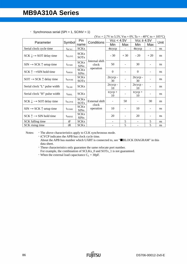
86
FUJITSU SEMICONDUCTOR CONFIDENTIAL r2.1
MB9A310A Series
DS706-00012-2v0-E
Synchronous serial (SPI = 1, SCINV = 1)
(Vcc = 2.7V to 5.5V, Vss = 0V, Ta = - 40°C to + 105°C) Vcc < 4.5V Vcc ≥ 4.5V
Parameter Symbol Pin
nameConditions
Min Max Min Max Unit
Serial clock cycle time tSCYC SCKx 4tcycp - 4tcycp - ns
SCK ↓→ SOT delay time tSLOVI SCKxSOTx
- 30 + 30 - 20 + 20 ns
SIN → SCK ↑ setup time tIVSHI SCKxSINx
50 - 30 - ns
SCK ↑ →SIN hold time tSHIXI SCKxSINx
0 - 0 - ns
SOT → SCK ↑ delay time tSOVHI SCKxSOTx
Internal shiftclock
operation
2tcycp - 30
- 2tcycp -
30 - ns
Serial clock "L" pulse width tSLSH SCKx2tcycp -
10 -
2tcycp - 10
- ns
Serial clock "H" pulse width tSHSL SCKxtcycp +
10 -
tcycp + 10
- ns
SCK ↓ → SOT delay time tSLOVE SCKxSOTx
- 50 - 30 ns
SIN → SCK ↑ setup time tIVSHE SCKxSINx
10 - 10 - ns
SCK ↑ → SIN hold time tSHIXE SCKxSINx
20 - 20 - ns
SCK falling time tF SCKx - 5 - 5 ns SCK rising time tR SCKx
External shiftclock
operation
- 5 - 5 ns
Notes: The above characteristics apply to CLK synchronous mode. tCYCP indicates the APB bus clock cycle time.
About the APB bus number which UART is connected to, see "BLOCK DIAGRAM" in this data sheet.
These characteristics only guarantee the same relocate port number. For example, the combination of SCLKx_0 and SOTx_1 is not guaranteed.
When the external load capacitance CL = 30pF.

87
FUJITSU SEMICONDUCTOR CONFIDENTIAL r2.1
MB9A310A Series
DS706-00012-2v0-E
tSCYC
tSLOVI
VOL
VOH VOH
VOH
VOL
VOH
VOL
VIH
VIL
VIH
VIL
tIVSHI tSHIXI
tSOVHI
MS bit = 0
tSHSLtR tSLSH tF
tSLOVE
VIL VILVILVIH VIHVIH
VOH
VOL
VOH
VOL
VIH
VIL
VIH
VIL
tIVSHE tSHIXE
MS bit = 1
External clock (EXT = 1) : asynchronous only
(Vcc = 2.7V to 5.5V, Vss = 0V, Ta = - 40°C to + 105°C)
Parameter Symbol Conditions Min Max Unit Remarks
Serial clock "L" pulse width tSLSH tcycp + 10 - ns Serial clock "H" pulse width tSHSL tcycp + 10 - ns SCK falling time tF - 5 ns SCK rising time tR
CL = 30pF
- 5 ns
tSHSL
VIL VIL VIL
VIH VIH VIH
tR tFtSLSH
SCK
SOT
SIN
SCK
SOT
SIN
SCK

88
FUJITSU SEMICONDUCTOR CONFIDENTIAL r2.1
MB9A310A Series
DS706-00012-2v0-E
(10) External input timing (Vcc = 2.7V to 5.5V, Vss = 0V, Ta = - 40°C to + 105°C)
Value Parameter Symbol Pin name Conditions
Min MaxUnit Remarks
ADTG A/D converter trigger input
FRCKx Free-run timer input clock
ICxx
- 2tCYCP*1 - ns
Input capture
DTTIxX - 2tCYCP*1 - ns Wave form generator
2tCYCP + 100*1 - ns
Input pulse width tINH tINL
INT00 to INT15,NMIX
- 500*2 - ns
External interrupt NMI
*1 : tCYCP indicates the APB bus clock cycle time except stop when in stop mode, in timer mode. About the APB bus number which the A/D converter, Multi-function Timer, External interrupt are
connected to, see "BLOCK DIAGRAM" in this data sheet. *2 : When in stop mode, in timer mode.
tINH tINL
VILS VILS
VIHS VIHS

89
FUJITSU SEMICONDUCTOR CONFIDENTIAL r2.1
MB9A310A Series
DS706-00012-2v0-E
(11) Quadrature Position/Revolution Counter timing (Vcc = 2.7V to 5.5V, Vss = 0V, Ta = - 40°C to + 105°C)
Value Parameter Symbol Conditions
Min Max Unit
AIN pin "H" width tAHL - AIN pin "L" width tALL - BIN pin "H" width tBHL - BIN pin "L" width tBLL - BIN rise time from AIN pin "H" level
tAUBU PC_Mode2 or
PC_Mode3 AIN fall time from BIN pin "H" level
tBUAD PC_Mode2 or
PC_Mode3 BIN fall time from AIN pin "L" level
tADBD PC_Mode2 or
PC_Mode3 AIN rise time from BIN pin "L" level
tBDAU PC_Mode2 or
PC_Mode3 AIN rise time from BIN pin "H" level
tBUAU PC_Mode2 or
PC_Mode3 BIN fall time from AIN pin "H" level
tAUBD PC_Mode2 or
PC_Mode3 AIN fall time from BIN pin "L" level
tBDAD PC_Mode2 or
PC_Mode3 BIN rise time from AIN pin "L" level
tADBU PC_Mode2 or
PC_Mode3 ZIN pin "H" width tZHL QCR:CGSC = "0" ZIN pin "L" width tZLL QCR:CGSC = "0" AIN/BIN rise and fall time from determined ZIN level
tZABE QCR:CGSC = "1"
Determined ZIN level from AIN/BIN rise and fall time
tABEZ QCR:CGSC = "1"
2tCYCP * - ns
* :tCYCP indicates the APB bus clock cycle time except stop. About the APB bus number which Quadrature Position/Revolution Counter is connected to, see "BLOCK DIAGRAM" in this data sheet.
tAHL
tBHL
tBLL
tALL
tAUBU tBUAD tADBD tBDAU
AIN
BIN

90
FUJITSU SEMICONDUCTOR CONFIDENTIAL r2.1
MB9A310A Series
DS706-00012-2v0-E
tBHL
tAHL
tALL
tBLL
tBUAU tAUBD tBDAD tADBU
tZHL
tZLL
tZABE
tABEZ
BIN
AIN
ZIN
ZIN
AIN/BIN

91
FUJITSU SEMICONDUCTOR CONFIDENTIAL r2.1
MB9A310A Series
DS706-00012-2v0-E
(12) I2C timing (Vcc = 2.7V to 5.5V, Vss = 0V, Ta = - 40°C to + 105°C)
Typical mode
High-speed mode Parameter Symbol Conditions
Min Max Min Max Unit Remarks
SCL clock frequency FSCL 0 100 0 400 kHz (Repeated) START condition hold time SDA ↓→ SCL ↓
tHDSTA 4.0 - 0.6 - μs
SCLclock "L" width tLOW 4.7 - 1.3 - μs SCLclock "H" width tHIGH 4.0 - 0.6 - μs (Repeated) START condition setup time SCL ↑ → SDA ↓
tSUSTA 4.7 - 0.6 - μs
Data hold time SCL ↓ → SDA ↓ ↑
tHDDAT 0 3.45*2 0 0.9*3 μs
Data setup time SDA ↓ ↑ → SCL ↑
tSUDAT 250 - 100 - ns
STOP condition setup time SCL ↑ → SDA ↑
tSUSTO 4.0 - 0.6 - μs
Bus free time between "STOP condition" and "START condition"
tBUF
CL = 30pF, R =
(Vp/IOL)*1
4.7 - 1.3 - μs
Noise filter tSP - 2 tCYCP*4 - 2 tCYCP*4 - ns *1 : R and C represent the pull-up resistor and load capacitance of the SCL and SDA lines, respectively. Vp
indicates the power supply voltage of the pull-up resistor and IOL indicates VOL guaranteed current. *2 : The maximum tHDDAT must satisfy that it does not extend at least "L" period (tLOW) of device's SCL signal. *3 : A high-speed mode I2C bus device can be used on a standard mode I2C bus system as long as the device
satisfies the requirement of "tSUDAT ≥ 250 ns". *4 : tCYCP is the APB bus clock cycle time.
About the APB bus number that I2C is connected to, see "BLOCK DIAGRAM" in this data sheet. To use I2C, set the APB bus clock at 8 MHz or more.
tLOW
tHDSTA tHDDAT tHIGH
tSUDATtSUSTA
tHDSTA tSP tSUSTO
tBUF
SDA
SCL

92
FUJITSU SEMICONDUCTOR CONFIDENTIAL r2.1
MB9A310A Series
DS706-00012-2v0-E
(13) ETM timing (Vcc = 2.7V to 5.5V, Vss = 0V, Ta = - 40°C to + 105°C)
Value Parameter Symbol Pin name Conditions
Min MaxUnit Remarks
Vcc ≥ 4.5V 2 9 Data hold tETMH
TRACECLKTRACED[3:0] Vcc < 4.5V 2 15
ns
Vcc ≥ 4.5V - 40 MHz TRACECLK frequency
1/tTRACE Vcc < 4.5V - 32 MHz
Vcc ≥ 4.5V 25 - ns TRACECLK Clock cycle time
tTRACE
TRACECLK
Vcc < 4.5V 31.25 - ns
Note: When the external load capacitance CL = 30pF.
tCYCC
tETMH
tTRACE
tETMH
VOH
VOH VOH
VOH
VOHVOL
VOL
VOH
VOL
HCLK
TRACECLK
TRACED[3:0]

93
FUJITSU SEMICONDUCTOR CONFIDENTIAL r2.1
MB9A310A Series
DS706-00012-2v0-E
(14) JTAG timing (Vcc = 2.7V to 5.5V, Vss = 0V, Ta = - 40°C to + 105°C)
Value Parameter Symbol Pin name Conditions
Min Max Unit Remarks
Vcc ≥ 4.5V TMS, TDI setup time
tJTAGS TCK
TMS,TDI Vcc < 4.5V 15 - ns
Vcc ≥ 4.5V TMS, TDI hold time tJTAGH
TCK TMS,TDI Vcc < 4.5V
15 - ns
Vcc ≥ 4.5V - 25 TDO delay time tJTAGD
TCK TDO Vcc < 4.5V - 45
ns
Note: When the external load capacitance CL = 30pF.
VOH
VOH
VOL
VOL
VOH
VOL
VOH
VOL
tJTAGS
tJTAGD
tJTAGH
TCK
TMS/TDI
TDO

94
FUJITSU SEMICONDUCTOR CONFIDENTIAL r2.1
MB9A310A Series
DS706-00012-2v0-E
5. 12-bit A/D Converter Electrical Characteristics for the A/D Converter
(Vcc = AVcc = 2.7V to 5.5V, Vss = AVss = 0V, Ta = - 40°C to + 105°C) Value
Parameter Pin
name Min Typ Max Unit Remarks
Resolution - - - 12 bit Non-linearity error - - 4.5 - + 4.5 LSBDifferential linearity error
- - 2.5 - + 2.5 LSB
Zero transition voltage AN0 to AN15
- 20 - + 20 mV
Full-scale transition voltage
AN0 to AN15
AVRH-20 - AVRH+20 mV
AVRH = 2.7V to 5.5V
Conversion time - 1.0*1 - - μs AVcc ≥ 4.5V *2 - - AVcc ≥ 4.5V
Sampling time Ts *2 - -
ns AVcc < 4.5V
Compare clock cycle*3 Tcck 50 - 2000 ns
State transition time to operation permission
Tstt 1.0 - - μs
- 0.57 0.72 mA A/D 1unit operation Power supply current (analog + digital)
AVCC - 0.06 20 μA When A/D stops
- 1.1 1.96 mAA/D 1unit operation AVRH = 5.5V
Reference power supply current (between AVRH and AVSS)
AVRH - 0.06 4 μA When A/D stops
Analog input capacity Cin - - 12.9 pF
2 AVcc ≥ 4.5V Analog input resistor Rin - -
3.8 kΩ
AVcc < 4.5V Interchannel disparity - - - 4 LSB Analog port input current
AN0 to AN15
- - 5 μA
Analog input voltage AN0 to AN15
AVSS - AVRH V
Reference voltage AVRH 2.7 - AVCC V *1: The conversion time is the value of sampling time (Ts) + compare time (Tc).
The condition of the minimum conversion time is when the value of sampling time: 300ns, the value of compare time: 700ns (AVcc ≥ 4.5V). Ensure that it satisfies the value of the sampling time (Ts) and compare clock cycle (Tcck). For setting of the sampling time and compare clock cycle, see "Chapter: A/D Converter" in "FM3 Family PERIPHERAL MANUAL Analog Macro Part". The A/D Converter register is set at APB bus clock timing. The sampling clock and compare clock are set at Base clock (HCLK).
*2: A necessary sampling time changes by external impedance. Ensure that it set the sampling time to satisfy (Equation 1)
*3: The compare time (Tc) is the value of (Equation 2)

95
FUJITSU SEMICONDUCTOR CONFIDENTIAL r2.1
MB9A310A Series
DS706-00012-2v0-E
Rext Rin
Cin
(Equation 1) Ts ≥ (Rin + Rext) × Cin × 9
Ts : Sampling time Rin : input resistor of A/D = 2kΩ 4.5 ≤ AVCC ≤ 5.5 input resistor of A/D = 3.8kΩ 2.7 ≤ AVCC < 4.5 Cin : input capacity of A/D = 12.9pF 2.7 ≤ AVCC ≤ 5.5 Rext : Output impedance of external circuit
(Equation 2) Tc = Tcck × 14
Tc : Compare time Tcck : Compare clock cycle
Analog signal source
AN0 to AN31 Analog input pin
Comparator

96
FUJITSU SEMICONDUCTOR CONFIDENTIAL r2.1
MB9A310A Series
DS706-00012-2v0-E
Definition of 12-bit A/D Converter Terms Resolution : Analog variation that is recognized by an A/D converter. Linearity error : Deviation of the line between the zero-transition point
(0b000000000000←→0b000000000001) and the full-scale transition point (0b111111111110←→0b111111111111) from the actual conversion characteristics.
Differential linearity error : Deviation from the ideal value of the input voltage that is required to change the output code by 1 LSB.
VNT - 1LSB × (N - 1) + VOT Linearity error of digital output N =
1LSB [LSB]
V(N + 1) T - VNTDifferential linearity error of digital output N =
1LSB - 1 [LSB]
VFST - VOT
1LSB = 4094
N : A/D converter digital output value. VOT : Voltage at which the digital output changes from 0x000 to 0x001. VFST : Voltage at which the digital output changes from 0xFFE to 0xFFF. VNT : Voltage at which the digital output changes from 0x(N − 1) to 0xN.
Linearity error Differential linearity error
Dig
ital o
utpu
t
Dig
ital o
utpu
t
Actual conversion characteristics Actual conversion
characteristics
Ideal characteristics (Actually-measured
value)
Actual conversioncharacteristics
Actual conversion characteristics
(Actually-measuredvalue)
(Actually-measured value)
Ideal characteristics (Actually-measuredvalue)
Analog input Analog input
(Actually-measuredvalue)
0x001
0x002
0x003
0x004
0xFFD
0xFFE
0xFFF
AVss AVRH AVss AVRH
0x(N-2)
0x(N-1)
0x(N+1)
0xN
1 LSB(N-1) + VOT
VNT
VFST
VOT
VNT
V(N+1)T

97
FUJITSU SEMICONDUCTOR CONFIDENTIAL r2.1
MB9A310A Series
DS706-00012-2v0-E
6. USB characteristics (Vcc = 2.7V to 5.5V,USBVcc = 3.0V to 3.6V, Vss = 0V, Ta = - 40°C to + 105°C)
Value Parameter Symbol
Pin name
ConditionsMin Max
Unit Remarks
Input High level voltage VIH - 2.0 USBVcc + 0.3 V *1
Input Low level voltage VIL - Vss - 0.3
0.8 V *1
Differential input sensitivity
VDI - 0.2 - V *2
Input charact- eristics
Different common mode range
VCM - 0.8 2.5 V *2
Output High level voltage VOH
External pull-down resistance= 15kΩ
2.8 3.6 V *3
Output Low level voltage VOL
External pull-up
resistance= 1.5kΩ
0.0 0.3 V *3
Crossover voltage VCRS - 1.3 2.0 V *4 Rising time tFR Full Speed 4 20 ns *5 Falling time tFF Full Speed 4 20 ns *5 Rise/fall time matching tFRFM Full Speed 90 111.11 % *5 Output impedance ZDRV Full Speed 28 44 Ω *6 Rising time tLR Low Speed 75 300 ns *7 Falling time tLF Low Speed 75 300 ns *7
Output charact- eristics
Rise/fall time matching tLRFM
UDP0,UDM0
Low Speed 80 125 % *7 *1 : The switching threshold voltage of Single-End-Receiver of USB I/O buffer is set as within VIL (Max) = 0.8V,
VIH (Min) = 2.0 V (TTL input standard). There are some hysteresis to lower noise sensitivity.
*2 : Use differential-Receiver to receive USB differential data signal.
Differential-Receiver has 200 mV of differential input sensitivity when the differential data input is within 0.8 V to 2.5 V to the local ground reference level. Above voltage range is the common mode input voltage range.
0.2
0.8
1.0
2.5 Common mode input voltage [V]
Min
imum
diff
eren
tial i
nput
se
nsiti
vity
[V]

98
FUJITSU SEMICONDUCTOR CONFIDENTIAL r2.1
MB9A310A Series
DS706-00012-2v0-E
*3 : The output drive capability of the driver is below 0.3 V at Low-State (VOL) (to 3.6 V and 1.5 kΩ load), and 2.8 V or above (to the ground and 1.5 kΩ load) at High-State (VOH).
*4 : The cross voltage of the external differential output signal (D + /D −) of USB I/O buffer is within 1.3 V to
2.0 V.
Max 2.0VD+
D-Min 1.3V
*5 : They indicate rising time (Trise) and falling time (Tfall) of the full-speed differential data signal.
They are defined by the time between 10% and 90% of the output signal voltage. For full-speed buffer, Tr/Tf ratio is regulated as within ± 10% to minimize RFI emission.
Rs=27ΩFull-speed Buffer
TxD+
TxD-
3-State Enable
Rs=27Ω
CL=50pF
CL=50pF
D+90%
Trise Tfall
90%
10%10%D-
VCRS specified range
Rising time Falling time

99
FUJITSU SEMICONDUCTOR CONFIDENTIAL r2.1
MB9A310A Series
DS706-00012-2v0-E
*6 : USB Full-speed connection is performed via twist pair cable shield with 90Ω ± 15% characteristic impedance(Differential Mode). USB standard defines that output impedance of USB driver must be in range from 28Ωto 44Ω. So, discrete series resistor (Rs) addition is defined in order to satisfy the above definition and keep balance. When using this USB FLS I/O, use it with 25Ω to 30Ω (recommendation value 27Ω) series resistor Rs.
Rs
Full-speed Buffer
TxD+
TxD-
3-State Enable
Rs
Rs series resistor 25Ω to 30Ω Series resistor of 27Ω (recommendation value) must be added. And, use "resistance with an uncertainty of 5% by E24 sequence".
*7 : They indicate rising time (Trise) and falling time (Tfall) of the low-speed differential data signal.
They are defined by the time between 10% and 90% of the output signal voltage.
D+
90%
Trise Tfall
90%
10%10%D-
See "· Low-Speed Load (Compliance Load)" for conditions of external load.
Mount it as external resistance.
28Ω to 44Ω Equiv. Imped.
28Ω to 44Ω Equiv. Imped.
Rising time Falling time

100
FUJITSU SEMICONDUCTOR CONFIDENTIAL r2.1
MB9A310A Series
DS706-00012-2v0-E
Low-Speed Load (Upstream Port Load) - Reference 1
Rs=27ΩLow-speed Buffer
TxD+
TxD-
3-State Enable
Rs=27Ω
Rpd
Rpd
Rpd=15kΩ
Low-Speed Load (Downstream Port Load) - Reference 2
Rs=27ΩLow-speed Buffer
TxD+
TxD-
3-State Enable
Rs=27Ω
Rpu=1.5kΩVTERM=3.6V
Rpu
VTERM
Low-Speed Load (Compliance Load)
Rs=27ΩLow-speed Buffer
TxD+
TxD-
3-State Enable
Rs=27Ω
CL = 50pF to 150pF
CL = 50pF to 150pF
CL =200pF to 600pF
CL =200pF to 600pF
CL = 200pF to 450pF
CL = 200pF to 450pF

101
FUJITSU SEMICONDUCTOR CONFIDENTIAL r2.1
MB9A310A Series
DS706-00012-2v0-E
7. Low-voltage detection characteristics
Low-voltage detection reset (Ta = - 40°C to + 105°C)
Value Parameter Symbol Conditions
Min Typ Max Unit Remarks
Detected voltage VDL - 2.25 2.45 2.65 V When voltage drops Released voltage VDH - 2.30 2.50 2.70 V When voltage rises
Interrupt of low-voltage detection (Ta = - 40°C to + 105°C)
Value Parameter Symbol Conditions
Min Typ Max Unit Remarks
Detected voltage VDL 2.58 2.8 3.02 V When voltage drops Released voltage VDH
SVHI = 00002.67 2.9 3.13 V When voltage rises
Detected voltage VDL 2.76 3.0 3.24 V When voltage drops Released voltage VDH
SVHI = 00012.85 3.1 3.34 V When voltage rises
Detected voltage VDL 2.94 3.2 3.45 V When voltage drops Released voltage VDH
SVHI = 00103.04 3.3 3.56 V When voltage rises
Detected voltage VDL 3.31 3.6 3.88 V When voltage drops Released voltage VDH
SVHI = 00113.40 3.7 3.99 V When voltage rises
Detected voltage VDL 3.40 3.7 3.99 V When voltage drops Released voltage VDH
SVHI = 01003.50 3.8 4.10 V When voltage rises
Detected voltage VDL 3.68 4.0 4.32 V When voltage drops Released voltage VDH
SVHI = 01113.77 4.1 4.42 V When voltage rises
Detected voltage VDL 3.77 4.1 4.42 V When voltage drops Released voltage VDH
SVHI = 10003.86 4.2 4.53 V When voltage rises
Detected voltage VDL 3.86 4.2 4.53 V When voltage drops Released voltage VDH
SVHI = 10013.96 4.3 4.64 V When voltage rises
LVD stabilization wait time
TLVDW - - - 2240 × tcycp *
μs
* : tCYCP indicates the APB2 bus clock cycle time.

102
FUJITSU SEMICONDUCTOR CONFIDENTIAL r2.1
MB9A310A Series
DS706-00012-2v0-E
8. Flash Memory Write/Erase Characteristics
(Vcc = 2.7V to 5.5V, Ta = - 40°C to + 105°C) Value
Parameter Min Typ Max
Value Remarks
Large Sector 0.7 3.7 Sector erase time
Small Sector -
0.3 1.1 s
Includes write time prior to internal erase
Half word (16 bit) write time
- 12 384 μs Not including system-level overhead time.
64K/128K/256KByte 5.2 23.6 s Chip erase time 384K/512KByte
- 8 38.4 s
Includes write time prior to internal erase
Write cycles and data hold time
Erase/write cycles (cycle)
Data hold time (year)
Remarks
1,000 20*
10,000 10*
100,000 5*
*:This value comes from the technology qualification (using Arrhenius equation to translate high temperature acceleration test result into average temperature value at + 85°C) .

103
FUJITSU SEMICONDUCTOR CONFIDENTIAL r4.0
MB9A310A Series
DS706-00012-2v0-E
ORDERING INFORMATION Part number Package
MB9AF311LAPMC1
MB9AF312LAPMC1
MB9AF314LAPMC1
Plastic LQFP(0.5mm pitch),64-pin (FPT-64P-M24/M38)
MB9AF311LAPMC
MB9AF312LAPMC
MB9AF314LAPMC
Plastic LQFP(0.65mm pitch),64-pin (FPT-64P-M23/M39)
MB9AF311LAQN
MB9AF312LAQN
MB9AF314LAQN
Plastic QFN(0.5mm pitch),64-pin (LCC-64P-M24)
MB9AF311MAPMC
MB9AF312MAPMC
MB9AF314MAPMC
MB9AF315MAPMC
MB9AF316MAPMC
Plastic LQFP(0.5mm pitch),80-pin (FPT-80P-M21/M37)
MB9AF311NAPMC
MB9AF312NAPMC
MB9AF314NAPMC
MB9AF315NAPMC
MB9AF316NAPMC
Plastic LQFP(0.5mm pitch),100-pin (FPT-100P-M20/M23)
MB9AF311NAPF
MB9AF312NAPF
MB9AF314NAPF
MB9AF315NAPF
MB9AF316NAPF
Plastic QFP(0.65mm pitch), 100-pin (FPT-100P-M06)
MB9AF311NABGL
MB9AF312NABGL
MB9AF314NABGL
Plastic PFBGA(0.8mm pitch),112-pin (BGA-112P-M04)
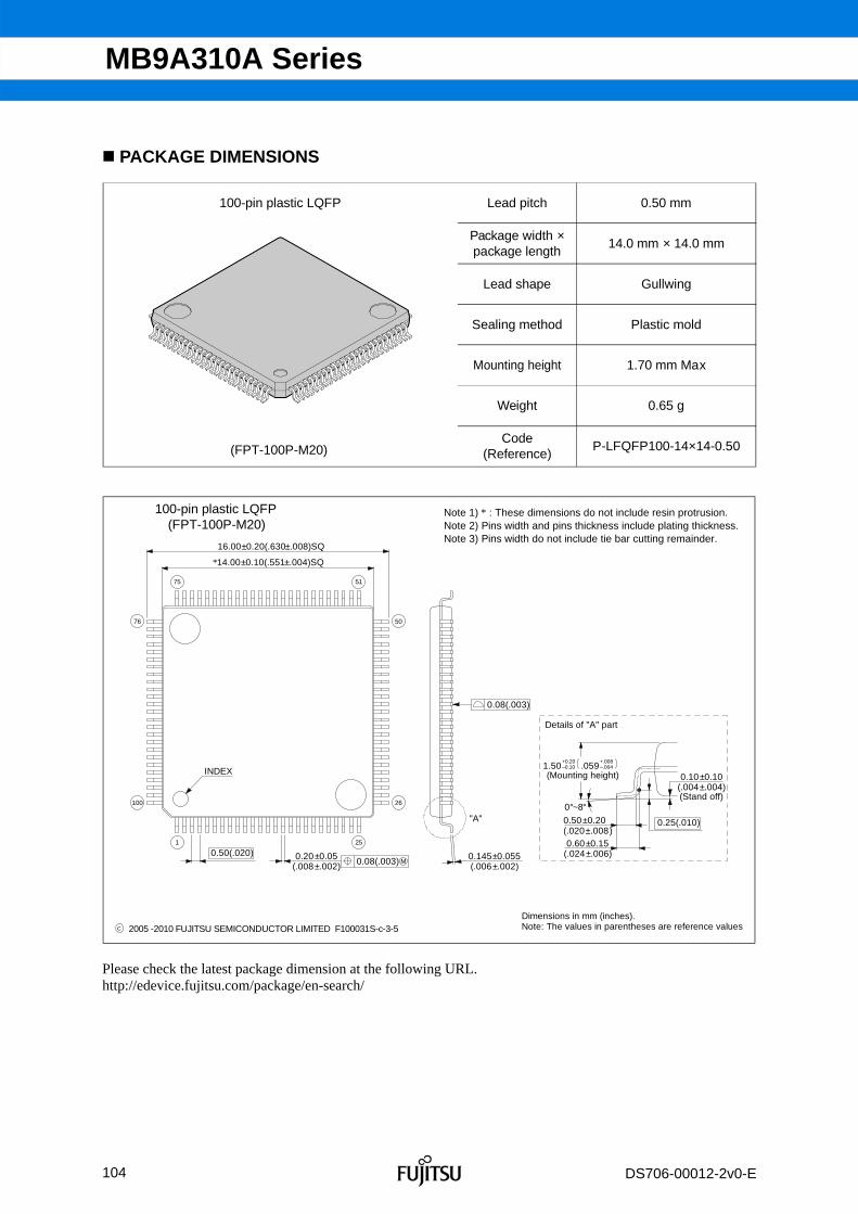
104
FUJITSU SEMICONDUCTOR CONFIDENTIAL r1.0
MB9A310A Series
DS706-00012-2v0-E
PACKAGE DIMENSIONS
100-pin plastic LQFP Lead pitch 0.50 mm
Package width ×package length
14.0 mm × 14.0 mm
Lead shape Gullwing
Sealing method Plastic mold
Mounting height 1.70 mm Max
Weight 0.65 g
Code(Reference)
P-LFQFP100-14×14-0.50
100-pin plastic LQFP(FPT-100P-M20)
(FPT-100P-M20)
C 2005 -2010 FUJITSU SEMICONDUCTOR LIMITED F100031S-c-3-5
16.00±0.20(.630±.008)SQ
1 25
26
51
76 50
75
100
0.50(.020) 0.20±0.05(.008±.002)
M0.08(.003) 0.145±0.055(.006±.002)
0.08(.003)
"A"
INDEX.059–.004
+.008–0.10+0.20
1.50(Mounting height)
0°~8°
0.50±0.20(.020±.008)
(.024±.006)0.60±0.15
0.25(.010)
0.10±0.10(.004±.004)
Details of "A" part
(Stand off)
*14.00±0.10(.551±.004)SQ
Dimensions in mm (inches).Note: The values in parentheses are reference values
Note 1) * : These dimensions do not include resin protrusion.Note 2) Pins width and pins thickness include plating thickness.Note 3) Pins width do not include tie bar cutting remainder.
Please check the latest package dimension at the following URL. http://edevice.fujitsu.com/package/en-search/

105
FUJITSU SEMICONDUCTOR CONFIDENTIAL r1.0
MB9A310A Series
DS706-00012-2v0-E
100-pin plastic LQFP Lead pitch 0.50 mm
Package width ×package length
14.00 mm × 14.00 mm
Lead shape Gullwing
Lead benddirection
Normal bend
Sealing method Plastic mold
Mounting height 1.70 mm MAX
Weight 0.65 g
100-pin plastic LQFP(FPT-100P-M23)
(FPT-100P-M23)
C 2009-2010 FUJITSU SEMICONDUCTOR LIMITED F100034S-c-3-4
16.00±0.20(.630±.008)SQ
1 25
51
76
75
100
0.50(.020) 0.22±0.05M0.08(.003)
*14.00±0.10(.551±.004)SQ
26
50
0.145±0.055(.006±.002)
0.08(.003)
"A"
INDEX
0°~8°
0.50±0.200.10±0.10
(Stand off)
+.008
+0.20
(Mounting height)
-0.101.50
.059 -.004( )
0.60±0.15 0.25(.010)
Dimensions in mm (inches).Note:The values in parentheses are reference values.
Note 1) * : These dimensions do not include resin protrusion.Note 2) Pins width and pins thickness include plating thickness.Note 3) Pins width do not include tie bar cutting remainder.
Details of "A" part
(.004±.004)
(.009±.002)
(.020±.008)
(.024±.006)
Please check the latest package dimension at the following URL. http://edevice.fujitsu.com/package/en-search/

106
FUJITSU SEMICONDUCTOR CONFIDENTIAL r1.0
MB9A310A Series
DS706-00012-2v0-E
100-pin plastic QFP Lead pitch 0.65 mm
Package width ×package length
14.00 × 20.00 mm
Lead shape Gullwing
Sealing method Plastic mold
Mounting height 3.35 mm MAX
Code(Reference)
P-QFP100-14×20-0.65
100-pin plastic QFP(FPT-100P-M06)
(FPT-100P-M06)
C 2002-2010 FUJITSU SEMICONDUCTOR LIMITED F100008S-c-5-7
1 30
31
50
5180
81
100
20.00±0.20(.787±.008)
23.90±0.40(.941±.016)
(.551±.008)
17.90±0.40(.705±.016)
INDEX
0.65(.026) 0.32±0.05(.013±.002)
M0.13(.005)
"A"
0.17±0.06(.007±.002)
0.10(.004)
Details of "A" part
(.035±.006)0.88±0.15
(.031±.008)0.80±0.20
0.25(.010)3.00
+0.35–0.20+.014–.008.118
(Mounting height)
0.25±0.20(.010±.008)(Stand off)
0~8°
*
*14.00±0.20
Dimensions in mm (inches).Note: The values in parentheses are reference values.
Note 1) * : These dimensions do not include resin protrusion.Note 2) Pins width and pins thickness include plating thickness.Note 3) Pins width do not include tie bar cutting remainder.
Please check the latest package dimension at the following URL. http://edevice.fujitsu.com/package/en-search/

107
FUJITSU SEMICONDUCTOR CONFIDENTIAL r1.0
MB9A310A Series
DS706-00012-2v0-E
80-pin plastic LQFP Lead pitch 0.50 mm
Package width ×package length
12 mm × 12 mm
Lead shape Gullwing
Sealing method Plastic mold
Mounting height 1.70 mm Max
Weight 0.47 g
Code(Reference)
P-LFQFP80-12×12-0.50
80-pin plastic LQFP(FPT-80P-M21)
(FPT-80P-M21)
C 2006-2010 FUJITSU SEMICONDUCTOR LIMITED F80035S-c-2-4
1 20
40
21
60 41
80
61
INDEX
12.00±0.10(.472±.004)SQ
14.00±0.20(.551±.008)SQ
0.50(.020) 0.20±0.05(.008±.002)
M0.08(.003)
0.145±0.055(.006±.002)
0.08(.003)
"A"
0°~8°
.059–.004+.008
–0.10+0.20
1.50
0.50±0.20(.020±.008)0.60±0.15
(.024±.006)
0.10±0.05(.004±.002)(Stand off)
0.25(.010)
Details of "A" part
LEAD No.
(Mounting height)
*
Dimensions in mm (inches).Note: The values in parentheses are reference values
Note 1) * : These dimensions do not include resin protrusion.Note 2) Pins width and pins thickness include plating thickness.Note 3) Pins width do not include tie bar cutting remainder.
Please check the latest package dimension at the following URL. http://edevice.fujitsu.com/package/en-search/
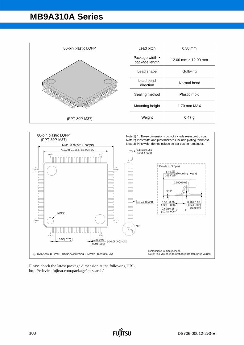
108
FUJITSU SEMICONDUCTOR CONFIDENTIAL r1.0
MB9A310A Series
DS706-00012-2v0-E
80-pin plastic LQFP Lead pitch 0.50 mm
Package width ×package length
12.00 mm × 12.00 mm
Lead shape Gullwing
Lead benddirection
Normal bend
Sealing method Plastic mold
Mounting height 1.70 mm MAX
Weight 0.47 g
80-pin plastic LQFP(FPT-80P-M37)
(FPT-80P-M37)
2009-2010 FUJITSU SEMICONDUCTOR LIMITED F80037S-c-1-2
1 20
40
21
60 41
80
61
INDEX
*12.00± 0.10(.472± .004)SQ
14.00± 0.20(.551± .008)SQ
0.50(.020) 0.22± 0.05
(.009± .002)M0.08(.003)
0.145± 0.055(.006± .002)
0.08(.003)
"A"
(Stand off)
Details of "A" part
(.004± .002)0.10± 0.05
(.024± .006)0.60± 0.15
(.020± .008)
0.25(.010)
0.50± 0.20
(Mounting height).059–.004
+.008
–0.10+0.201.50
0~8°
C
Dimensions in mm (inches).Note: The values in parentheses are reference values.
Note 1) * : These dimensions do not include resin protrusion.Note 2) Pins width and pins thickness include plating thickness.Note 3) Pins width do not include tie bar cutting remainder.
Please check the latest package dimension at the following URL. http://edevice.fujitsu.com/package/en-search/

109
FUJITSU SEMICONDUCTOR CONFIDENTIAL r1.0
MB9A310A Series
DS706-00012-2v0-E
64-pin plastic LQFP Lead pitch 0.50 mm
Package width ×package length
10.0 × 10.0 mm
Lead shape Gullwing
Sealing method Plastic mold
Mounting height 1.70 mm MAX
Weight 0.32 g
Code(Reference)
P-LFQFP64-10×10-0.50
64-pin plastic LQFP(FPT-64P-M24)
(FPT-64P-M24)
LEAD No.
Details of "A" part
0.25(.010)
(Stand off)
0.10±0.10
0.60±0.15(.024±.006)
0.50±0.20(.020±.008)
1.50+0.20–0.10
+.008–.004.059
0°~8°
"A"
0.08(.003)
0.145±0.055(.006±.002)
0.08(.003) M(.008±.002)
0.20±0.050.50(.020)
12.00±0.20(.472±.008)SQ
INDEX
49
64
3348
17
32
161
2005-2010 FUJITSU SEMICONDUCTOR LIMITED F64036S-c-1-3C
(Mounting height)
*10.00±0.10(.394±.004)SQ
Dimensions in mm (inches).Note: The values in parentheses are reference values
Note 1) * : These dimensions do not include resin protrusion.Note 2) Pins width and pins thickness include plating thickness.Note 3) Pins width do not include tie bar cutting remainder.
(.004±.004)
Please check the latest package dimension at the following URL. http://edevice.fujitsu.com/package/en-search/

110
FUJITSU SEMICONDUCTOR CONFIDENTIAL r1.0
MB9A310A Series
DS706-00012-2v0-E
64-pin plastic LQFP Lead pitch 0.50 mm
Package width ×package length
10.00 mm × 10.00 mm
Lead shape Gullwing
Lead benddirection
Normal bend
Sealing method Plastic mold
Mounting height 1.70 mm MAX
Weight 0.32 g
64-pin plastic LQFP(FPT-64P-M38)
(FPT-64P-M38)
"A"
0.08(.003)
0.145 ± 0.055(.006 ± .002)
0.08(.003) M0.22±0.050.50(.020)
12.00±0.20(.472±.008)SQ
*10.00±0.10(.394±.004)SQ
INDEX
49
64
3348
17
32
161
2010 FUJITSU SEMICONDUCTOR LIMITED F64038S-c-1-2
(Stand off)
Details of "A" part
0.10 ± 0.10(.004±.004)
0.60 ± 0.15
0.25(.010)
C
0.50±0.20(.020±.008)
(Mounting height).059–.004
+.008
–0.10+0.201.50
0~8°
Dimensions in mm (inches).Note: The values in parentheses are reference values.
Note 1) * : These dimensions do not include resin protrusion.Note 2) Pins width and pins thickness include plating thickness.Note 3) Pins width do not include tie bar cutting remainder.
(.009±.002)
(.024±.006)
Please check the latest package dimension at the following URL. http://edevice.fujitsu.com/package/en-search/

111
FUJITSU SEMICONDUCTOR CONFIDENTIAL r1.0
MB9A310A Series
DS706-00012-2v0-E
64-pin plastic LQFP Lead pitch 0.65 mm
Package width ×package length
12.0 × 12.0 mm
Lead shape Gullwing
Sealing method Plastic mold
Mounting height 1.70 mm MAX
Weight 0.47 g
Code(Reference)
P-LQFP64-12 × 12-0.65
64-pin plastic LQFP(FPT-64P-M23)
(FPT-64P-M23)
C 2003-2010 FUJITSU SEMICONDUCTOR LIMITED F64034S-c-1-4
0.65(.026)
0.10(.004)
1 16
17
3249
64
3348
*12.00± 0.10(.472± .004)SQ
14.00± 0.20(.551± .008)SQ
INDEX
0.32± 0.05(.013± .002)
M0.13(.005)
0.145± 0.055(.006± .002)
"A"
.059–.004+.008
–0.10+0.20
1.50
0~8°
0.25(.010)
(Mounting height)
0.50± 0.20(.020± .008)0.60± 0.15
(.024± .006)
0.10± 0.10(.004± .004)
Details of "A" part
(Stand off)
Dimensions in mm (inches).Note: The values in parentheses are reference values
Note 1) * : These dimensions do not include resin protrusion.Note 2) Pins width and pins thickness include plating thickness.Note 3) Pins width do not include tie bar cutting remainder.
Please check the latest package dimension at the following URL. http://edevice.fujitsu.com/package/en-search/

112
FUJITSU SEMICONDUCTOR CONFIDENTIAL r1.0
MB9A310A Series
DS706-00012-2v0-E
64-pin plastic LQFP Lead pitch 0.65 mm
Package width ×package length
12.00 mm × 12.00 mm
Lead shape Gullwing
Sealing method Plastic mold
Mounting height 1.70 mm MAX
Weight 0.47 g
64-pin plastic LQFP(FPT-64P-M39)
(FPT-64P-M39)
"A"
0.10(.004)
0.145±0.055(.006±.002)
0.13(.005) M0.32±0.050.65(.026)
14.00±0.20(.551±.008)SQ
12.00±0.10(.472±.004)SQ
INDEX
49
64
3348
17
32
161
2010-2011 FUJITSU SEMICONDUCTOR LIMITED HMbF64-39Sc-2-2
Details of "A" part
0.10±0.10
0.60±0.15(.024±.006)
0.25(.010)BSC
C
.059–.004+.008
–0.10+0.201.50
0~8˚
0.50±0.20
Dimensions in mm (inches).Note: The values in parentheses are referencevalues.
Note 1) Pins width and pins thickness include plating thickness.
(.013±.002)
(.020±.008)
(.004±.004)
Please check the latest package dimension at the following URL. http://edevice.fujitsu.com/package/en-search/

113
FUJITSU SEMICONDUCTOR CONFIDENTIAL r1.0
MB9A310A Series
DS706-00012-2v0-E
112-ball plastic PFBGA Ball pitch 0.80 mm
Package width ×package length
10.00 × 10.00 mm
Lead shape Soldering ball
Sealing method Plastic mold
Ball size Ф 0.45 mm
Mounting height 1.45 mm Max.
Weight 0.22 g
112-ball plastic PFBGA(BGA-112P-M04)
(BGA-112P-M04)
C 2003-2010 FUJITSU SEMICONDUCTOR LIMITED B112004S-c-2-3
10.00±0.10(.394±.004)
(.049±.008)1.25±0.20
(Seated height)
6
F
INDEX(INDEX AREA)
10.00±0.10(.394±.004)
(112-Ф0.18±.004)112-Ф0.45±010
0.35±0.10(.014±.004)(Stand off)
0.10(.004) S
B
A
GHJKL E D C B A
7
8
9
10
11
5
4
32
1
0.80(.031)REF
REF0.80(.031)
Ф0.08(.003) BASM
0.20(.008) S B
S
AS0.20(.008)
Dimensions in mm (inches).Note: The values in parentheses are reference values.
Please check the latest package dimension at the following URL. http://edevice.fujitsu.com/package/en-search/

114
FUJITSU SEMICONDUCTOR CONFIDENTIAL r1.0
MB9A310A Series
DS706-00012-2v0-E
64-pin plastic QFN Lead pitch 0.50 mm
Package width ×package length
9.00 mm × 9.00 mm
Sealing method Plastic mold
Mounting height 0.90 mm MAX
Weight -
64-pin plastic QFN(LCC-64P-M24)
(LCC-64P-M24)
C 2011 FUJITSU SEMICONDUCTOR LIMITED HMbC64-24Sc-2-1
(.354±.004)9.00±0.10
(.236±.004)6.00±0.10
(.236±.004)6.00±0.10
(.354±.004)9.00±0.10
0.40±0.05(.016±.002)
0.50 (.020)(TYP)
0.25±0.05(.010±.002)
0.45 (.018)
1PIN ID(0.20R (.008R))
0.05 (.002) MAX (0.20 (.008))
0.85±0.05(.033±.002)
INDEX AREA
Dimensions in mm (inches).Note: The values in parentheses are reference values.
Please check the latest package dimension at the following URL. http://edevice.fujitsu.com/package/en-search/

115
FUJITSU SEMICONDUCTOR CONFIDENTIAL r3.0
MB9A310A Series
DS706-00012-2v0-E
MAJOR CHANGES IN THIS EDITION A change on a page is indicated by a vertical line drawn on the left side of that page.
Page Section Change Results
- -
Revised series name and part number: MB9A310 Series → MB9A310A Series MB9AF311L → MB9AF311LA MB9AF312L → MB9AF312LA MB9AF314L → MB9AF314LA MB9AF311M → MB9AF311MA MB9AF312M → MB9AF312MA MB9AF314M → MB9AF314MA MB9AF315M → MB9AF315MA MB9AF316M → MB9AF316MA MB9AF311N → MB9AF311NA MB9AF312N → MB9AF312NA MB9AF314N → MB9AF314NA MB9AF315N → MB9AF315NA MB9AF316N → MB9AF316NA Added the following package.
LCC-64P-M24
PRODUCT LINEUPFunction Multi-function Serial
Added the following description. ch.4 to ch.7: FIFO (16steps × 9-bit) ch.0 to ch.3: No FIFO 7
External Interrupts Corrected the following description. 7pins (Max) → 8pins (Max)
34 to 37 SIGNAL DESCRIPTION Multi-function Serial (ch.0 to ch.7)
Corrected the description for function. Added "LIN pin" Deleted "UART pin"
42, 43
I/O CIRCUIT TYPE Corrected the following schematic for "TypeB". CMOS level hysteresis input → Digital input Corrected the following schematic for "TypeC".
Control Pin → Digital output
51 HANDLING DEVICE Power supply pins
Corrected the description.
54 MEMORY SIZE Added "MEMORY SIZE ".
69 ELECTRICAL CHARACTERISTICS 4. AC Characteristics (1)Main Clock input Characteristics
Added the items FCM to the Internal operating clock frequency.
71 (4-2) Operating Conditions of Main PLL
72 (7) External Bus Timing External bus clock output Characteristics
Added the description.
79 (8) Base Timer Input Timing Trigger input timing
Added the Note.
88 (10) External input timing Corrected the footnote.

116
FUJITSU MICROELECTRONICS CONFIDENTIAL r2.0
MB9A310A Series
Page Section Change Results
94
5. 12-bit A/D Converter (1) Electrical characteristics for the A/D converter
Corrected the value of "Full-scale transition voltage". Min: -20 → AVRH-20 Max: +20 → AVRH+20 Corrected the value of "Compare clock cycle".
Max: 10000 → 2000 Corrected the value of "Reference voltage".
Min: AVSS → 2.7
117
FUJITSU SEMICONDUCTOR CONFIDENTIAL r3.0
MB9A310A Series
DS706-00012-2v0-E

118
FUJITSU MICROELECTRONICS CONFIDENTIAL r2.0
MB9A310A Series

119
FUJITSU SEMICONDUCTOR CONFIDENTIAL r3.0
MB9A310A Series
DS706-00012-2v0-E

120
FUJITSU MICROELECTRONICS CONFIDENTIAL r2.0
MB9A310A Series
FUJITSU SEMICONDUCTOR LIMITED Nomura Fudosan Shin-yokohama Bldg. 10-23, Shin-yokohama 2-Chome, Kohoku-ku Yokohama Kanagawa 222-0033, Japan Tel: +81-45-415-5858 http://jp.fujitsu.com/fsl/en/
For further information please contact:
North and South America FUJITSU SEMICONDUCTOR AMERICA, INC. 1250 E. Arques Avenue, M/S 333 Sunnyvale, CA 94085-5401, U.S.A. Tel: +1-408-737-5600 Fax: +1-408-737-5999 http://us.fujitsu.com/micro/ Europe FUJITSU SEMICONDUCTOR EUROPE GmbH Pittlerstrasse 47, 63225 Langen, Germany Tel: +49-6103-690-0 Fax: +49-6103-690-122 http://emea.fujitsu.com/semiconductor/ Korea FUJITSU SEMICONDUCTOR KOREA LTD. 902 Kosmo Tower Building, 1002 Daechi-Dong, Gangnam-Gu, Seoul 135-280, Republic of Korea Tel: +82-2-3484-7100 Fax: +82-2-3484-7111 http://kr.fujitsu.com/fsk/
Asia Pacific FUJITSU SEMICONDUCTOR ASIA PTE. LTD. 151 Lorong Chuan, #05-08 New Tech Park 556741 Singapore Tel : +65-6281-0770 Fax : +65-6281-0220 http://sg.fujitsu.com/semiconductor/ FUJITSU SEMICONDUCTOR SHANGHAI CO., LTD. 30F, Kerry Parkside, 1155 Fang Dian Road, Pudong District, Shanghai 201204, China Tel : +86-21-6146-3688 Fax : +86-21-6146-3660 http://cn.fujitsu.com/fss/ FUJITSU SEMICONDUCTOR PACIFIC ASIA LTD. 10/F., World Commerce Centre, 11 Canton Road, Tsimshatsui, Kowloon, Hong Kong Tel : +852-2377-0226 Fax : +852-2376-3269 http://cn.fujitsu.com/fsp/
Specifications are subject to change without notice. For further information please contact each office. All Rights Reserved. The contents of this document are subject to change without notice. Customers are advised to consult with sales representatives before ordering. The information, such as descriptions of function and application circuit examples, in this document are presented solely for the purpose of reference to show examples of operations and uses of FUJITSU SEMICONDUCTOR device; FUJITSU SEMICONDUCTOR does not warrant proper operation of the device with respect to use based on such information. When you develop equipment incorporating the device based on such information, you must assume any responsibility arising out of such use of the information. FUJITSU SEMICONDUCTOR assumes no liability for any damages whatsoever arising out of the use of the information.Any information in this document, including descriptions of function and schematic diagrams, shall not be construed as license of the use or exercise of any intellectual property right, such as patent right or copyright, or any other right of FUJITSU SEMICONDUCTOR or any third party or does FUJITSU SEMICONDUCTOR warrant non-infringement of any third-party's intellectual property right or other right by using such information. FUJITSU SEMICONDUCTOR assumes no liability for any infringement of the intellectual property rights or other rights of third parties which would result from the use of information contained herein. The products described in this document are designed, developed and manufactured as contemplated for general use, including without limitation, ordinary industrial use, general office use, personal use, and household use, but are not designed, developed and manufactured as contemplated (1) for use accompanying fatal risks or dangers that, unless extremely high safety is secured, could have a serious effect to the public, and could lead directly to death, personal injury, severe physical damage or other loss (i.e., nuclear reaction control in nuclear facility, aircraft flight control, air traffic control, mass transport control, medical life support system, missile launch control in weapon system), or (2) for use requiring extremely high reliability (i.e., submersible repeater and artificial satellite). Please note that FUJITSU SEMICONDUCTOR will not be liable against you and/or any third party for any claims or damages arising in connection with above-mentioned uses of the products. Any semiconductor devices have an inherent chance of failure. You must protect against injury, damage or loss from such failures by incorporating safety design measures into your facility and equipment such as redundancy, fire protection, and prevention of over-current levels and other abnormal operating conditions. Exportation/release of any products described in this document may require necessary procedures in accordance with the regulations of the Foreign Exchange and Foreign Trade Control Law of Japan and/or US export control laws. The company names and brand names herein are the trademarks or registered trademarks of their respective owners.
Edited: Sales Promotion Department