spansion flash memory tm -...
TRANSCRIPT

September 2003
This document specifies SPANSION memory products that are now offered by both Advanced Micro Devices andFujitsu. Although the document is marked with the name of the company that originally developed the specification,these products will be offered to customers of both AMD and Fujitsu.
Continuity of Specifications There is no change to this datasheet as a result of offering the device as a SPANSION product. Future routinerevisions will occur when appropriate, and changes will be noted in a revision summary.
Continuity of Ordering Part NumbersAMD and Fujitsu continue to support existing part numbers beginning with "Am" and "MBM". To order these products, please use only the Ordering Part Numbers listed in this document.
For More InformationPlease contact your local AMD or Fujitsu sales office for additional information about SPANSION memory solutions.
TM
TM
TM
SPANSION Flash Memory Data Sheet
TM

DS05-20842-4EFUJITSU SEMICONDUCTORDATA SHEET
Embedded Erase™, Embedded Program™ and ExpressFlash™ are trademarks of Advanced Micro Devices, Inc.
FLASH MEMORYCMOS
4M (512K × 8) BIT
MBM29F040C-55/-70/-90
FEATURES• Single 5.0 V read, program and erase
Minimizes system level power requirements• Compatible with JEDEC-standard commands
Uses same software commands as E2PROMs• Compatible with JEDEC-standard byte-wide pinouts
32-pin PLCC (Package suffix: PD)32-pin TSOP(I) (Package suffix: PF)32-pin TSOP(I) (Package suffix: PFTN – Normal Bend Type, PFTR – Reversed Bend Type)
• Minimum 100,000 write/erase cycles• High performance
55 ns maximum access time• Sector erase architecture
8 equal size sectors of 64K bytes eachAny combination of sectors can be concurrently erased. Also supports full chip erase.
• Embedded Erase™ AlgorithmsAutomatically pre-programs and erases the chip or any sector
• Embedded Program™ AlgorithmsAutomatically writes and verifies data at specified address
• Data Polling and Toggle Bit feature for detection of program or erase cycle completion• Low V CC write inhibit ≤ 3.2 V• Sector protection
Hardware method disables any combination of sectors from write or erase operations• Erase Suspend/Resume
Suspends the erase operation to allow a read data in another sector within the same device
2
MBM29F040C-55/-70/-90
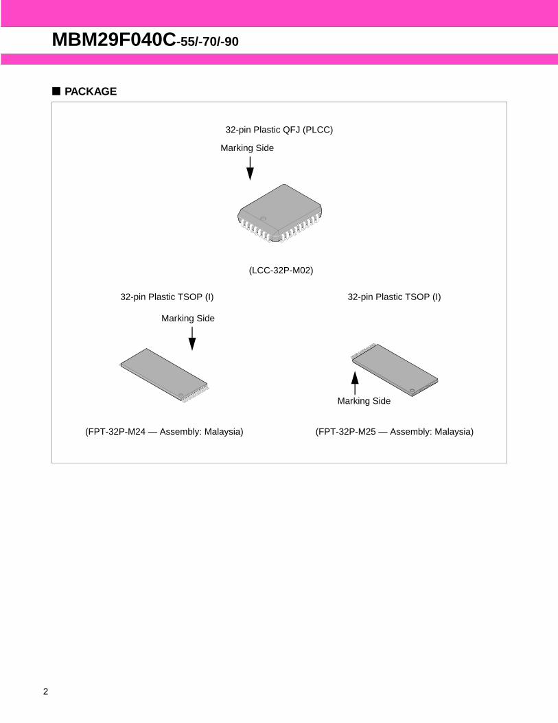
PACKAGE
Marking Side
(LCC-32P-M02)
(FPT-32P-M24 — Assembly: Malaysia) (FPT-32P-M25 — Assembly: Malaysia)
Marking Side
Marking Side
32-pin Plastic QFJ (PLCC)
32-pin Plastic TSOP (I) 32-pin Plastic TSOP (I)

MBM29F040C-55/-70/-90
GENERAL DESCRIPTION
The MBM29F040C is a 4M-bit, 5.0 V-only Flash memory organized as 512K bytes of 8 bits each. The MBM29F040C is offered in a 32-pin PLCC and 32-pin TSOP(I) package. This device is designed to be programmed in-system with the standard system 5.0 V VCC supply. A 12.0 V VPP is not required for write or erase operations. The device can also be reprogrammed in standard EPROM programmers.
The standard MBM29F040C offers access times 55 ns and 90 ns, allowing operation of high-speed microprocessors without wait states. To eliminate bus contention the device has separate chip enable (CE), write enable (WE), and output enable (OE) controls.
The MBM29F040C is pin and command set compatible with JEDEC standard E2PROMs. Commands are written to the command register using standard microprocessor write timings. Register contents serve as input to an internal state-machine which controls the erase and programming circuitry. Write cycles also internally latch addresses and data needed for the programming and erase operations. Reading data out of the device is similar to reading from 12.0 V Flash or EPROM devices.
The MBM29F040C is programmed by executing the program command sequence. This will invoke the Embedded Program Algorithm which is an internal algorithm that automatically times the program pulse widths and verifies proper cell margin. Typically, each sector can be programmed and verified in less than 0.5 seconds. Erase is accomplished by executing the erase command sequence. This will invoke the Embedded Erase Algorithm which is an internal algorithm that automatically preprograms the array if it is not already programmed before executing the erase operation. During erase, the device automatically times the erase pulse widths and verifies proper cell margin.
Any individual sector is typically erased and verified in 1 second. (If already completely preprogrammed.)
The device also features a sector erase architecture. The sector mode allows for 64K byte sectors of memory to be erased and reprogrammed without affecting other sectors. The MBM29F040C is erased when shipped from the factory.
The device features single 5.0 V power supply operation for both read and write functions. Internally generated and regulated voltages are provided for the program and erase operations. A low VCC detector automatically inhibits write operations on the loss of power. The end of program or erase is detected by Data Polling of DQ7 or by the Toggle Bit feature on DQ6. Once the end of a program or erase cycle has been completed, the device internally resets to the read mode.
Fujitsu's Flash technology combines years of EPROM and E2PROM experience to produce the highest levels of quality, reliability and cost effectiveness. The MBM29F040C memory electrically erases the entire chip or all bits within a sector simultaneously via Fowler-Nordheim tunneling. The bytes are programmed one byte at a time using the EPROM programming mechanism of hot electron injection.
3

4
MBM29F040C-55/-70/-90
• 64K Byte per sector• Individual-sector, multiple-sector, or bulk-erase
capability• Individual or multiple-sector protection is user
definable 64K byte per sector
7FFFFH
6FFFFH
5FFFFH
4FFFFH
3FFFFH
2FFFFH
1FFFFH
0FFFFH
00000H
FLEXIBLE SECTOR-ERASE ARCHITECTURE
MBM29F040C-55/-70/-90
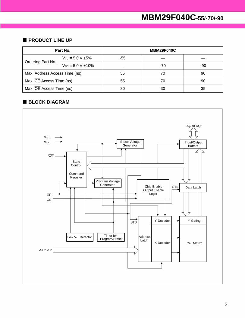
PRODUCT LINE UP
BLOCK DIAGRAM
Part No. MBM29F040C
Ordering Part No.VCC = 5.0 V ±5% -55 — —
VCC = 5.0 V ±10% — -70 -90
Max. Address Access Time (ns) 55 70 90
Max. CE Access Time (ns) 55 70 90
Max. OE Access Time (ns) 30 30 35
VSS
VCC
WE
CE
A0 to A18
OE
Erase VoltageGenerator
DQ0 to DQ7
StateControl
CommandRegister
Program VoltageGenerator
Low VCC Detector AddressLatch
X-Decoder
Y-Decoder
Cell Matrix
Y-Gating
Chip EnableOutput Enable
Logic
Data Latch
Input/OutputBuffers
STB
STB
Timer for Program/Erase
5

6
MBM29F040C-55/-70/-90
CONNECTION DIAGRAMS
A11
A9
A8
A13
A14
A17
WEVCC
A18
A16
A15
A12
A7
A6
A5
A4
OEA10
CEDQ7
DQ6
DQ5
DQ4
DQ3
V SS
DQ2
DQ1
DQ0
A0
A1
A2
A3
A4
A5
A6
A7
A12
A15
A16
A18
VCC
WEA17
A14
A13
A8
A9
A11
A3
A2
A1
A0
DQ0
DQ1
DQ2
VSS
DQ3
DQ4
DQ5
DQ6
DQ7
CEA10
OE
12345678910111213141516
32313029282726252423222120191817
16151413121110987654321
17181920212223242526272829303132
MBM29F040CStandard Pinout
MBM29F040CReverse Pinout
TSOP (I)
A7
A6
A5
A4
A3
A2
A1
A0
DQ0
A14
A13
A8
A9
A11
OE
A10
CE
DQ7
5
6
7
8
9
10
11
12
13
29
28
27
26
25
24
23
22
21
4 3 2 1 32 31 30
14 15 16 17 18 19 20
DQ
1
DQ
2
VS
S
DQ
3
DQ
4
DQ
5
DQ
6
PLCC
A12
A15
A16 A18
V C
C
WE
A17
LCC-32P-M02
FPT-32P-M24
FPT-32P-M25
Marking Side
Marking Side

MBM29F040C-55/-70/-90
LOGIC SYMBOL
Legend: L = VIL, H = VIH, X = VIL or VIH, = Pulse Input. See DC Characteristics for voltage levels.
Notes: 1. Manufacturer and device codes may also be accessed via a command register write sequence. SeeTable 5.
2. Refer to the section on Sector Protection.3. WE can be VIL if OE is VIL, OE at VIH initiates the write operations.
Table 1 MBM29F040C Pin Configuration
Pin Function
A0 to A18 Address Inputs
DQ0 to DQ7 Data Inputs/Outputs
CE Chip Enable
OE Output Enable
WE Write Enable
VSS Device Ground
VCC Device Power Supply
Table 2 MBM29F040C User Bus Operations
Operation CE OE WE A0 A1 A6 A9 I/O
Auto-Select Manufacturer Code (1) L L H L L L VID Code
Auto-Select Device Code (1) L L H H L L VID Code
Read (3) L L H A0 A1 A6 A9 DOUT
Standby H X X X X X X HIGH-Z
Output Disable L H H X X X X HIGH-Z
Write (Program/Erase) L H L A0 A1 A6 A9 DIN
Enable Sector Protection (2) L VID X X X VID X
Verify Sector Protection (2) L L H L H L VID Code
19
A0 to A18
WE
OE
CE
DQ0 to DQ7
8
7

8
MBM29F040C-55/-70/-90
ORDERING INFORMATION
Standard Products
Fujitsu standard products are available in several packages. The order number is formed by a combination of:
MBM29F040 C -55 PD
DEVICE NUMBER/DESCRIPTIONMBM29F0404Mega-bit (512K × 8-Bit) CMOS Flash Memory5.0 V-only Read, Program, and Erase64K Byte Sectors
PACKAGE TYPEPD =32-Pin Rectangular Plastic Leaded Chip
Carrier (PLCC)PFTN = 32-Pin Thin Small Outline Package
(TSOP) Standard PinoutPFTR =32-Pin Thin Small Outline Package
(TSOP) Reverse Pinout
SPEED OPTIONSee Product Selector Guide
C = Device Revision

MBM29F040C-55/-70/-90
FUNCTIONAL DESCRIPTION
Read Mode
The MBM29F040C has two control functions which must be satisfied in order to obtain data at the outputs. CE is the power control and should be used for a device selection. OE is the output control and should be used to gate data to the output pins if a device is selected.
Address access time (tACC) is equal to the delay from stable addresses to valid output data. The chip enable access time (tCE) is the delay from stable addresses and stable CE to valid data at the output pins. The output enable access time is the delay from the falling edge of OE to valid data at the output pins (assuming the addresses have been stable for at least tACC-tOE time).
Standby Mode
The MBM29F040C has two standby modes, a CMOS standby mode (CE input held at VCC ±0.3 V.), when the current consumed is less than 5 µA; and a TTL standby mode (CE is held at VIH) when the current required is reduced to approximately 1 mA. During Embedded Algorithm operation, VCC Active current (ICC2) is required even CE = VIH. The device can be read with standard access time (tCE) from either of these standby modes. In the standby mode the outputs are in a high impedance state, independent of the OE input.
If the device is deselected during erasure or programming, the device will draw active current until the operation is completed.
Output Disable
With the OE input at a logic high level (VIH), output from the device is disabled. This will cause the output pins to be in a high impedance state.
Autoselect
The autoselect mode allows the reading out of a binary code from the device and will identify its manufacturer and type. This mode is intended for use by programming equipment for the purpose of automatically matching the device to be programmed with its corresponding programming algorithm. This mode is functional over the entire temperature range of the device.
To activate this mode, the programming equipment must force VID (11.5 V to 12.5 V) on address pin A9. Two identifier bytes may then be sequenced from the device outputs by toggling address A0 from VIL to VIH. All addresses are DON’T CARES except A0, A1, and A6. (Recommend VIL for the other pins.)
The manufacturer and device codes may also be read via the command register, for instances when the MBM29F040C is erased or programmed in a system without access to high voltage on the A9 pin. The command sequence is illustrated in Table 5. (Refer to Autoselect Command section.)
Byte 0 (A0 = VIL) represents the manufacture’s code (Fujitsu = 04H) and byte 1 (A0 = VIH) represents the device identifier code (MBM29F040C = A4H). These two bytes are given in the Table 3. All identifiers for manufactures and device will exhibit odd parity with the MSB (DQ7) defined as the parity bit. In order to read the proper device codes when executing the autoselect, A1 must be VIL. (See Table 3.)
9

10
MBM29F040C-55/-70/-90
* : Outputs 01H at protected sector addresses and 00H at unprotected sector addresses.
Write
Device erasure and programming are accomplished via the command register. The contents of the register serve as inputs to the internal state machine. The state machine outputs dictate the function of the device.
The command register itself does not occupy any addressable memory location. The register is a latch used to store the commands, along with the address and data information needed to execute the command. The command register is written by bringing WE to VIL, while CE is at VIL and OE is at VIH. Addresses are latched on the falling edge of WE or CE, whichever happens later; while data is latched on the rising edge of WE or CE, whichever happens first. Standard microprocessor write timings are used.
Refer to AC Write Characteristics and the Erase/Programming Waveforms for specific timing parameters.
Sector Protection
The MBM29F040C features hardware sector protection. This feature will disable both program and erase operations in any number of sectors (0 through 8). The sector protection feature is enabled using programming equipment at the user’s site. The device is shipped with all sectors unprotected.
To activate this mode, the programming equipment must force VID on address pin A9 and control pin OE, (suggest VID = 11.5 V) and CE = VIH. The sector addresses (A18, A17 and A16) should be set to the sector to be protected. Table 4 defines the sector address for each of the eight (8) individual sectors. Programming of the protection circuitry begins on the falling edge of the WE pulse and is terminated with the rising edge of the same. Sector addresses must be held constant during the WE pulse. See figures 11 and 17 sector protection waveforms and algorithm.
Table 3 MBM29F040C Sector Protection Verify Autoselect Codes
Type A 18 A17 A16 A6 A1 A0Code (HEX) DQ7 DQ6 DQ5 DQ4 DQ3 DQ2 DQ1 DQ0
Manufacture’sCode X X X VIL VIL VIL 04H 0 0 0 0 0 1 0 0
Device Code X X X VIL VIL VIH A4H 1 0 1 0 0 1 0 0
Sector Protection
SectorAddresses VIL VIH VIL 01H* 0 0 0 0 0 0 0 1
Table 4 Sector Address Tables
Sector Address A 18 A17 A16 Address Range
SA0 0 0 0 00000H to 0FFFFH
SA1 0 0 1 10000H to 1FFFFH
SA2 0 1 0 20000H to 2FFFFH
SA3 0 1 1 30000H to 3FFFFH
SA4 1 0 0 40000H to 4FFFFH
SA5 1 0 1 50000H to 5FFFFH
SA6 1 1 0 60000H to 6FFFFH
SA7 1 1 1 70000H to 7FFFFH

MBM29F040C-55/-70/-90
To verify programming of the protection circuitry, the programming equipment must force VID on address pin A9 with CE and OE at VIL and WE at VIH. Scanning the sector addresses (A16, A17 and A18) while (A6, A1, A0) = (0, 1, 0) will produce a logical “1” code at device output DQ0 for a protected sector. Otherwise the device will read 00H for unprotected sector. In this mode, the lower order addresses, except for A0, A1 and A6 are DON’T CARES. Address locations with A1 = VIL are reserved for Autoselect manufacturer and device codes.
It is also possible to determine if a sector is protected in the system by writing an Autoselect command. Performing a read operation at the address location XX02H, where the higher order addresses (A16, A17 and A18) are the sector address will produce a logical “1” at DQ0 for a protected sector. See Table 3 for Autoselect codes.
Notes: 1. Address bits A11 to A18 = X = “H” or “L” for all address commands except for Program Address (PA) and Sector Address (SA).
2. Bus operations are defined in Table 2.3. RA = Address of the memory location to be read.
PA = Address of the memory location to be programmed. Addresses are latched on the falling edge of theWE pulse.
SA = Address of the sector to be erased. The combination of A18, A17, and A16 will uniquely select any sector.
4. RD = Data read from location RA during read operation.PD = Data to be programmed at location PA. Data is latched on the falling edge of WE.
*: Either of the two reset commands will reset the device.
Command Definitions
Device operations are selected by writing specific address and data sequences into the command register. Writing incorrect address and data values or writing them in the improper sequence will reset the device to read mode. Table 5 defines the valid register command sequences. Note that the Erase Suspend (B0H) and Erase Resume (30H) commands are valid only while the Sector Erase operation is in progress. Moreover, both Read/Reset Commands are functionally equivalent, resetting the device to the read mode.
Table 5 MBM29F040C Command Definitions
CommandSequence
Read/Reset
BusWrite
CyclesReq'd
First BusWrite Cycle
Second BusWrite Cycle
Third BusWrite Cycle
Fourth BusRead/Write
CycleFifth Bus
Write CycleSixth Bus
Write Cycle
Addr Data Addr Data Addr Data Addr Data Addr Data Addr Data
Read/Reset* 1 XXXH F0H — — — — — — — — — —
Read/Reset* 4 555H AAH 2AAH 55H 555H F0H RA RD — — — —
Autoselect 3 555H AAH 2AAH 55H 555H 90H — — — — — —
Byte Program 4 555H AAH 2AAH 55H 555H A0H PA PD — — — —
Chip Erase 6 555H AAH 2AAH 55H 555H 80H 555H AAH 2AAH 55H 555H 10H
Sector Erase 6 555H AAH 2AAH 55H 555H 80H 555H AAH 2AAH 55H SA 30H
Sector Erase Suspend Erase can be suspended during sector erase with Addr (“H” or “L”). Data (B0H)
Sector Erase Resume Erase can be resumed after suspend with Addr (“H” or “L”). Data (30H)
11

12
MBM29F040C-55/-70/-90
Read/Reset Command
The read or reset operation is initiated by writing the Read/Reset command sequence into the command register. Microprocessor read cycles retrieve array data from the memory. The device remains enabled for reads until the command register contents are altered.
The device will automatically power-up in the read/reset state. In this case, a command sequence is not required to read data. Standard microprocessor read cycles will retrieve array data. This default value ensures that no spurious alteration of the memory content occurs during the power transition. Refer to the AC Read Characteristics and Waveforms for the specific timing parameters.
Autoselect Command
Flash memories are intended for use in applications where the local CPU alters memory contents. As such, manufacture and device codes must be accessible while the device resides in the target system. PROM programmers typically access the signature codes by raising A9 to a high voltage (VID = 11.5 V to 12.5). However, multiplexing high voltage onto the address lines is not generally desired system design practice.
The device contains an Autoselect command operation to supplement traditional PROM programming methodology. The operation is initiated by writing the Autoselect command sequence into the command register. Following the command write, a read cycle from address XX00H retrieves the manufacture code of 04H. A read cycle from address XX01H returns the device code A4H. (see Table 3.) All manufacturer and device codes will exhibit odd parity with the MSB (DQ7) defined as the parity bit.Sector state (protection or unprotection) will be informed address XX02H.Scanning the sector addresses (A16, A17, A18) while (A6, A1, A0) = (0, 1, 0) will produce a logical “1” at device output DQ0 for a protected sector. The programming verification should be perform margin mode on the protected sector. (See Table 2 and 3.)To terminate the operation, it is necessary to write the Read/Reset command sequence into the register, and also to write the Autoselect command during the operation, execute it after writing Read/Reset command sequence.
Byte Programming
The device is programmed on a byte-by-byte basis. Programming is a four bus cycle operation. There are two “unlock” write cycles. These are followed by the program setup command and data write cycles. Addresses are latched on the falling edge of CE or WE, whichever happens later and the data is latched on the rising edge of CE or WE, whichever happens first. The rising edge of CE or WE (whichever happens first) begins programming. Upon executing the Embedded Program Algorithm command sequence, the system is not required to provide further controls or timings. The device will automatically provide adequate internally generated program pulses and verify the programmed cell margin.
The automatic programming operation is completed when the data on DQ7 is equivalent to data written to this bit (See Write Operation Status section.) at which time the device returns to the read mode and addresses are no longer latched. (See Table 6, Hardware Sequence Flags.) Therefore, the device requires that a valid address to the device be supplied by the system at this particular instance of time. Hence, Data Polling must be performed at the memory location which is being programmed.
Any commands written to the chip during this period will be ignored.
Programming is allowed in any sequence and across sector boundaries. Beware that a data “0” cannot be programmed back to a “1”. Attempting to do so may either hang up the device (Exceed timing limits.), or result in an apparent success according to the data polling algorithm but a read from reset/read mode will show that the data is still “0”. Only erase operations can convert “0”s to “1”s.
Figure 13 illustrates the Embedded ProgramTM Algorithm using typical command strings and bus operations.

MBM29F040C-55/-70/-90
Chip Erase
Chip erase is a six bus cycle operation. There are two “unlock” write cycles. These are followed by writing the “set-up” command. Two more “unlock” write cycles are then followed by the chip erase command.
Chip erase does not require the user to program the device prior to erase. Upon executing the Embedded Erase Algorithm command sequence the device will automatically program and verify the entire memory for an all zero data pattern prior to electrical erase. The system is not required to provide any controls or timings during these operations.
The automatic erase begins on the rising edge of the last WE pulse in the command sequence and terminates when the data on DQ7 is “1” (see Write Operation Status section.) at which time the device returns to read the mode.
Figure 14 illustrates the Embedded Erase Algorithm using typical command strings and bus operations.
Sector Erase
Sector erase is a six bus cycle operation. There are two “unlock” write cycles. These are followed by writing the “set-up” command. Two more “unlock” write cycles are then followed by the Sector Erase command. The sector address (Any address location within the desired sector.) is latched on the falling edge of WE, while the command (Data = 30H) is latched on the rising edge of WE. A time-out of 50 µs from the rising edge of the last sector erase command will initiate the sector erase command(s).
Multiple sectors may be erased concurrently by writing the six bus cycle operations as described above. This sequence is followed with writes of the Sector Erase command to addresses in other sectors desired to be concurrently erased. The time between writes must be less than 50 µs, otherwise that command will not be accepted. It is recommended that processor interrupts be disabled during this time to guarantee this condition. The interrupts can be re-enabled after the last Sector Erase command is written. A time-out of 50 µs from the rising edge of the last WE will initiate the execution of the Sector Erase command(s). If another falling edge of the WE occurs within the 50 µs time-out window the timer is reset. (Monitor DQ3 to determine if the sector erase timer window is still open, see section DQ3, Sector Erase Timer.) Any command other than Sector Erase or Erase Suspend during this time-out period will reset the device to read mode, ignoring the previous command string. Resetting the device once execution has begun will corrupt the data in the sector. In that case, restart the erase on those sectors and allow them to complete. (Refer to the Write Operation Status section for Sector Erase Timer operation.) Loading the sector erase buffer may be done in any sequence and with any number of sectors (1 to 7).
Sector erase does not require the user to program the device prior to erase. The device automatically programs all memory locations in the sector(s) to be erased prior to electrical erase. When erasing a sector or sectors the remaining unselected sectors are not affected. The system is not required to provide any controls or timings during these operations.
The automatic sector erase begins after the 50 µs time out from the rising edge of the WE pulse for the last sector erase command pulse and terminates when the data on DQ7 is “1” (See Write Operation Status section.) at which time the device returns to read mode. During the execution of the Sector Erase command, only the Erase Suspend and Erase Resume commands are allowed. All other commands will reset the device to read mode. Data polling must be performed at an address within any of the sectors being erased.
Figure 14 illustrates the Embedded EraseTM Algorithm using typical command strings and bus operations.
13

14
MBM29F040C-55/-70/-90
Erase Suspend
The Erase Suspend command allows the user to interrupt a Sector Erase operation and then perform data reads from or programs to a sector not being erased. This command is applicable ONLY during the Sector Erase operation which include the time-out period for sector erase. The Erase Suspend command will be ignored if written during the Chip Erase operation or Embedded Program Algorithm. Writting the Erase Suspend command during the Sector Erase time-out results in immediate termination of the time-out period and suspension of the erase operation.
Any other command written during the Erase Suspend mode will be ignored except the Erase Resume command. Writing the Erase Resume command resumes the erase operation. The addresses are “DON’T CARES” when writing the Erase Suspend or Erase Resume command.
When the Erase Suspend command is written during the Sector Erase operation, the device will take a maximum of 10 µs to suspend the erase operation. When the devices have entered the erase-suspended mode, the DQ7 bit will be at logic “1”, and DQ6 will stop toggling. The user must use the address of the erasing sector for reading DQ6 and DQ7 to determine if the erase operation has been suspended. Further writes of the Erase Suspend command are ignored.
When the erase operation has been suspended, the devices default to the erase-suspend-read mode. Reading data in this mode is the same as reading from the standard read mode except that the data must be read from sectors that have not been erase-suspended. Successively reading from the erase-suspended sector while the device is in the erase-suspend-read mode will cause DQ2 to toggle. (See the section on DQ2.)
After entering the erase-suspend-read mode, the user can program the device by writing the appropriate command sequence for Program. This Program mode is known as the erase-suspend-program mode. Again, programming in this mode is the same as programming in the regular Program mode except that the data must be programmed to sectors that are not erase-suspended. Successively reading from the erase-suspended sector while the devices are in the erase-suspend-program mode will cause DQ2 to toggle. The end of the erase-suspended Program operation is detected by Data polling of DQ7, or by the Toggle Bit I (DQ6) which is the same as the regular Program operation. Note that DQ7 must be read from the Program address while DQ6 can be read from any address.
To resume the operation of Sector Erase, the Resume command (30H) should be written. Any further writes of the Resume command at this point will be ignored. Another Erase Suspend command can be written after the chip has resumed erasing.

MBM29F040C-55/-70/-90
Write Operation Status
Notes: 1. Performing successive read operations from any address will cause DQ6 to toggle.2. Reading the byte address being programmed while in the erase-suspend program mode will indicate logic
“1” at the DQ2 bit. However, successive reads from the erase-suspended sector will cause DQ2 to toggle.3. DQ0 and DQ1 are reserve pins for future use. DQ4 is for Fujitsu internal use only.
DQ7
Data Polling
The MBM29F040C device features Data Polling as a method to indicate to the host that the Embedded Algorithms are in progress or completed. During the Embedded Program Algorithm an attempt to read the device will produce the compliment of the data last written to DQ7. Upon completion of the Embedded Program Algorithm, an attempt to read the device will produce the true data last written to DQ7. During the Embedded Erase Algorithm, an attempt to read the device will produce a “0” at the DQ7 output. Upon completion of the Embedded Erase Algorithm an attempt to read the device will produce a “1” at the DQ7 output. The flowchart for Data Polling (DQ7) is shown in Figure 15.
For chip erase, and sector erase the Data Polling is valid after the rising edge of the sixth WE pulse in the six write pulse sequence. For sector erase, the Data Polling is valid after the last rising edge of the sector erase WE pulse. Data Polling must be performed at sector address within any of the sectors being erased and not a protected sector. Otherwise, the status may not be valid. Once the Embedded Algorithm operation is close to being completed, the MBM29F040C data pins (DQ7) may change asynchronously while the output enable (OE) is asserted low. This means that the device is driving status information on DQ7 at one instant of time and then that byte’s valid data at the next instant of time. Depending on when the system samples the DQ7 output, it may read the status or valid data. Even if the device has completed the Embedded Algorithm operation and DQ7 has a valid data, the data outputs on DQ0 to DQ6 may be still invalid. The valid data on DQ0 to DQ7 will be read on the successive read attempts.
The Data Polling feature is only active during the Embedded Programming Algorithm, Embedded Erase Algorithm, or sector erase time-out. (See Table 6.)
See Figure 9 for the Data Polling timing specifications and diagrams.
Table 6 Hardware Sequence Flags
Status DQ 7 DQ6 DQ5 DQ3 DQ2
In Progress
Embedded Program Algorithm DQ7 Toggle 0 0 1
Embedded Erase Algorithm 0 Toggle 0 1 Toggle
Erase Suspended Mode
Erase Suspend Read(Erase Suspended Sector) 1 1 0 0 Toggle
Erase Suspend Read(Non-Erase Suspended Sector) Data Data Data Data Data
Erase Suspend Program Non-Erase Suspended Sector) DQ7
Toggle(Note 1) 0 0 1
(Note 2)
ExceededTime Limits
Embedded Program Algorithm DQ7 Toggle 1 0 1
Program/Erase in Embedded Erase Algorithm 0 Toggle 1 1 N/A
Erase Suspended Mode
Erase Suspend Program(Non-Erase Suspended Sector) DQ7 Toggle 1 0 N/A
15

16
MBM29F040C-55/-70/-90
DQ6
Toggle Bit I
The MBM29F040C also features the “Toggle Bit I” as a method to indicate to the host system that the Embedded Algorithms are in progress or completed.
During an Embedded Program or Erase Algorithm cycle, successive attempts to read (OE toggling) data from the device will result in DQ6 toggling between one and zero. Once the Embedded Program or Erase Algorithm cycle is completed, DQ6 will stop toggling and valid data will be read on the next successive attempts. During programming, the Toggle Bit I is valid after the rising edge of the fourth WE pulse in the four write pulse sequence. For chip erase and sector erase, the Toggle Bit I is valid after the rising edge of the sixth WE pulse in the six write pulse sequence. The Toggle Bit I is active during the sector time out.
In programming, if the sector being written to is protected, the toggle bit will toggle for about 2 µs and then stop toggling without the data having changed. In erase, the device will erase all the selected sectors except for the ones that are protected. If all selected sectors are protected, the chip will toggle the toggle bit for about 100 µs and then drop back into read mode, having changed none of the data.
Either CE or OE toggling will cause the DQ6 to toggle. In addition, an Erase Suspend/Resume command will cause the DQ6 to toggle.
See Figure 10 for the Toggle Bit timing specifications and diagrams.
DQ5
Exceeded Timing Limits
DQ5 will indicate if the program or erase time has exceeded the specified limits (internal pulse count). Under these conditions DQ5 will produce a “1”. This is a failure condition which indicates that the program or erase cycle was not successfully completed. Data Polling DQ7, DQ6 is the only operating function of the device under this condition. The CE circuit will partially power down the device under these conditions (to approximately 2 mA). The OE and WE pins will control the output disable functions as described in Table 2.
The DQ5 failure condition may also appear if a user tries to program a non blank location without erasing. In this case the device locks out and never completes the Embedded Algorithm operation. Hence, the system never reads a valid data on DQ7 bit and DQ6 never stops toggling. Once the device has exceeded timing limits, the DQ5 bit will indicate a “1.” Please note that this is not a device failure condition since the device was incorrectly used. If this occurs, reset the device with command sequence.
DQ3
Sector Erase Timer
After the completion of the initial sector erase command sequence the sector erase time-out will begin. DQ3 will remain low until the time-out is complete. Data Polling and Toggle Bit I are valid after the initial sector erase command sequence.
If Data Polling or the Toggle Bit I indicates the device has been written with a valid erase command. DQ3 may be used to determine if the sector erase timer window is still open. If DQ3 is high (“1”) the internally controlled erase cycle has begun; attempts to write subsequent commands to the device will be ignored until the erase operation is completed as indicated by Data Polling or Toggle Bit I. If DQ3 is low (“0”), the device will accept additional sector erase commands. To insure the command has been accepted, the system software should check the status of DQ3 prior to and following each subsequent sector erase command. If DQ3 were high on the second status check, the command may not have been accepted.
Refer to Table 6: Hardware Sequence Flags.

MBM29F040C-55/-70/-90
DQ2
Toggle Bit II
This Toggle Bit II, along with DQ6, can be used to determine whether the devices are in the Embedded Erase Algorithm or in Erase Suspend.
Successive reads from the erasing sector will cause DQ2 to toggle during the Embedded Erase Algorithm. If the devices are in the erase-suspended-read mode, successive reads from the erase-suspended sector will cause DQ2 to toggle. When the devices are in the erase-suspended-program mode, successive reads from the byte address of the non-erase suspended sector will indicate a logic “1” at the DQ2 bit.
DQ6 is different from DQ2 in that DQ6 toggles only when the standard program or Erase, or Erase Suspend Program operation is in progress. The behavior of these two status bits, along with that of DQ7, is summarized as follows:
Notes: 1. These status flags apply when outputs are read from a sector that has been erase-suspended.2. These status flags apply when outputs are read from the byte address of the non-erase suspended sector.
Data Protection
The MBM29F040C is designed to offer protection against accidental erasure or programming caused by spurious system level signals that may exist during power transitions. During power up the device automatically resets the internal state machine in the Read mode. Also, with its control register architecture, alteration of the memory contents only occurs after successful completion of specific multi-bus cycle command sequences.
The device also incorporates several features to prevent inadvertent write cycles resulting form VCC power-up and power-down transitions or system noise.
Low V CC Write Inhibit
To avoid initiation of a write cycle during VCC power-up and power-down, a write cycle is locked out for VCC less than 3.2 V (typically 3.7 V). If VCC < VLKO, the command register is disabled and all internal program/erase circuits are disabled. Under this condition the device will reset to the read mode. Subsequent writes will be ignored until the VCC level is greater than VLKO.
Write Pulse “Glitch” Protection
Noise pulses of less than 5 ns (typical) on OE, CE, or WE will not initiate a write cycle.
Logical Inhibit
Writing is inhibited by holding any one of OE = VIL, CE = VIH, or WE = VIH. To initiate a write cycle CE and WE must be a logical zero while OE is a logical one.
Mode DQ7 DQ6 DQ2
Program DQ7 toggles 1
Erase 0 toggles toggles
Erase Suspend Read (Erase-Suspended Sector)(Note 1)
1 1 toggles
Erase Suspend Program DQ7 (Note 2) toggles 1 (Note 2)
17

18
MBM29F040C-55/-70/-90
Power-Up Write Inhibit
Power-up of the device with WE = CE = VIL and OE = VIH will not accept commands on the rising edge of WE. The internal state machine is automatically reset to the read mode on power-up.
MBM29F040C-55/-70/-90
ABSOLUTE MAXIMUM RATINGS
Storage Temperature .................................................................................... –55°C to +125°CAmbient Temperature with Power Applied .................................................... –40°C to +85°CVoltage with Respect to Ground All pins except A9, OE (Note 1).................. –2.0 V to +7.0 VVCC (Note 1) .................................................................................................. –2.0 V to +7.0 VA9, OE (Note 2) ............................................................................................. –2.0 V to +13.5 V
Notes: 1. Minimum DC voltage on input or I/O pins is –0.5 V. During voltage transitions, inputs may negative overshoot VSS to –2.0 V for periods of up to 20 ns. Maximum DC voltage on output and I/O pins is VCC +0.5 V. During voltage transitions, outputs may positive overshoot to VCC +2.0 V for periods of up to 20 ns.
2. Minimum DC input voltage on A9 and OE pins are –0.5 V. During voltage transitions, A9 and OE pins may negative overshoot VSS to –2.0 V for periods of up to 20 ns. Maximum DC input voltage on A9 and OE pins are +13.5 V which may overshoot to 14.0 V for periods of up to 20 ns.
WARNING: Semiconductor devices can be permanently damaged by application of stress (voltage, current, temperature, etc.) in excess of absolute maximum ratings. Do not exceed these ratings.
RECOMMENDED OPERATING RANGESAmbient Temperature (TA) ................................................................................ –40°C to +85°CVCC Supply Voltages
MBM29F040C-55.......................................................................................... +4.75 V to +5.25 VMBM29F040C-70/-90 ................................................................................... +4.50 V to +5.50 V
Operating ranges define those limits between which the functionality of the device is guaranteed.
WARNING: The recommended operating conditions are required in order to ensure normal operation of the semiconductor device. All of the device’s electrical characteristics are warranted when the device is operated within these ranges.Always use semiconductor devices within their recommended operating condition ranges. Operation outside these ranges may adversely affect reliability and could result in device failure.No warranty is made with respect to uses, operating conditions, or combinations not represented onthe data sheet. Users considering application outside the listed conditions are advised to contact theirFUJITSU representatives beforehand.
19

20
MBM29F040C-55/-70/-90
MAXIMUM OVERSHOOT
Figure 1 Maximum Negative Overshoot Waveform
+0.8 V
–0.5 V
20 ns
–2.0 V20 ns
20 ns
Figure 2 Maximum Positive Overshoot Waveform 1
+2.0 V
VCC+0.5 V
20 ns
VCC+2.0 V20 ns
20 ns
VCC+0.5 V
+13.0 V
20 ns
+14.0 V20 ns
20 ns
Figure 3 Maximum Positive Overshoot Waveform 2
* : This waveform is applied for A9, OE.

MBM29F040C-55/-70/-90
DC CHARACTERISTICS
Notes: 1. The ICC current listed includes both the DC operating current and the frequency dependent component (at 6 MHz). The frequency component typically is 2 mA/MHz, with OE at VIH.
2. ICC active while Embedded Algorithm (program or erase) is in progress.3. Applicable to sector protection function.4. (VID – VCC) do not exceed 9 V.
ParameterSymbol Parameter Description Test Conditions Min. Max. Unit
ILI Input Leakage Current VIN = VSS to VCC, VCC = VCC Max — ±1.0 µA
ILO Output Leakage Current VOUT = VSS to VCC, VCC = VCC Max — ±1.0 µA
ILIT A9, OE Input Leakage Current VCC = VCC Max., A9, OE = 12.0 V — 50 µA
ICC1 VCC Active Current (Note 1) CE = VIL, OE = VIH — 30 mA
ICC2 VCC Active Current (Note 2) CE = VIL, OE = VIH — 45 mA
ICC3 VCC Current (Standby)VCC = VCC Max., CE = VIH — 1 mA
VCC = VCC Max., CE = VCC±0.3 V — 5 µA
VIL Input Low Level — –0.5 0.8 V
VIH Input High Level — 2.0 VCC+0.3 V
VIDVoltage for Autoselect and Sector Protection (A9, OE) (Note 3, 4) VCC = 5.0 V 11.5 12.5 V
VOL Output Low Voltage Level IOL = 12.0 mA, VCC = VCC Min — 0.45 V
VOH1
Output High Voltage LevelIOH = –2.5 mA, VCC = VCC Min 2.4 — V
VOH2 IOH = –100 µA VCC–0.4 — V
VLKO Low VCC Lock-Out Voltage — 3.2 4.2 V
21

22
MBM29F040C-55/-70/-90
AC CHARACTERISTICS
• Read Only Operations Characteristics
Note: 1. Test Conditions:Output Load: 1 TTL gate and 30 pFInput rise and fall times: 5 nsInput pulse levels: 0.0 V to3.0 VTiming measurement reference level
Input: 1.5 VOutput: 1.5 V
ParameterSymbols Description Test Setup -55
(Note1)-70
(Note2)-90
(Note2) UnitJEDEC Standard
tAVAV tRC Read Cycle Time — Min. 55 70 90 ns
tAVQV tACC Address to Output Delay CE = VIL
OE = VILMax. 55 70 90 ns
tELQV tCE Chip Enable to Output Delay OE = VIL Max. 55 70 90 ns
tGLQV tOE Output Enable to Output Delay — Max. 30 30 35 ns
tEHQZ tDF Chip Enable to Output HIGH-Z — Max. 20 20 20 ns
tGHQZ tDF Output Enable to Output HIGH-Z — Max. 20 20 20 ns
tAXQX tOH
Output Hold Time From Addresses,CE or OE, Whichever Occurs First
— Min. 0 0 0 ns
Figure 4 Test Conditions
CL
5.0 V
Diodes = IN3064or Equivalent
2.7 kΩDeviceUnderTest
IN3064or Equivalent
6.2 kΩ
Note: 1.CL = 30 pF including jig capacitance2.CL = 100 pF including jig capacitance
Note: 2. Test Conditions:Oput Load: 1 TTL gate and 100 pFInput rise and fall times: 5 nsInput pulse levels: 0.45 V to 2.4 VTiming measurement reference level Input: 0.8 and 2.0 V Output: 0.8 and 2.0 V

MBM29F040C-55/-70/-90
• Write/Erase/Program Operations
Notes: 1. This does not include the preprogramming time.2. This timing is only for Sector Protect operations.
Parameter SymbolsDescription
MBM29F040CUnit
JEDEC Standard -55 -70 -90
tAVAV tWC Write Cycle Time Min. 55 70 90 ns
tAVWL tAS Address Setup Time Min. 0 0 0 ns
tWLAX tAH Address Hold Time Min. 40 45 45 ns
tDVWH tDS Data Setup Time Min. 25 30 45 ns
tWHDX tDH Data Hold Time Min. 0 0 0 ns
— tOES Output Enable Setup Time Min. 0 0 0 ns
— tOEHOutput Enable Hold Time
Read Min. 0 0 0 ns
Toggle and Data Polling Min. 10 10 10 ns
tGHWL tGHWL Read Recover Time Before Write Min. 0 0 0 ns
tGHEL tGHEL Read Recover Time Before Write Min. 0 0 0 ns
tELWL tCS CE Setup Time Min. 0 0 0 ns
tWLEL tWS WE Setup Time Min. 0 0 0 ns
tWHEH tCH CE Hold Time Min. 0 0 0 ns
tEHWH tWH WE Hold Time Min. 0 0 0 ns
tWLWH tWP Write Pulse Width Min. 30 35 45 ns
tELEH tCP CE Pulse Width Min. 30 35 45 ns
tWHWL tWPH Write Pulse Width High Min. 20 20 20 ns
tEHEL tCPH CE Pulse Width High Min. 20 20 20 ns
tWHWH1 tWHWH1 Byte Programming Operation Typ. 8 8 8 µs
tWHWH2 tWHWH2 Sector Erase Operation (Note 1)Typ. 1 1 1 sec
Max. 8 8 8 sec
— tVCS VCC Setup Time Min. 50 50 50 µs
— tVLHT Voltage Transition Time (Notes 2) Min. 4 4 4 µs
— tWPP Write Pulse Width (Note 2) Min. 100 100 100 µs
— tOESP OE Setup Time to WE Active (Note 2) Min. 4 4 4 µs
— tCSP CE Setup Time to WE Active (Note 2) Min. 4 4 4 µs
— tEOE Delay Time from Embedded Output Enable Max. 30 30 35 ns
23

24
MBM29F040C-55/-70/-90
SWITCHING WAVEFORMS
• Key to Switching Waveforms
Figure 5 AC Waveforms for Read Operations
WAVEFORM INPUTS OUTPUTS
Must BeSteady
MayChangefrom H to L
MayChangefrom L to H
“H” or “L”Any ChangePermitted
Does NotApply
Will BeSteady
Will BeChangingfrom H to L
Will BeChangingfrom L to H
ChangingStateUnknown
Center Line isHigh-Impedance“Off” State
WE
OE
CE
tACC
tDF
tOHtCE
tOE
Outputs
tRC
Addresses Addresses Stable
High-ZOutput Valid
High-Z
tOEH
MBM29F040C-55/-70/-90
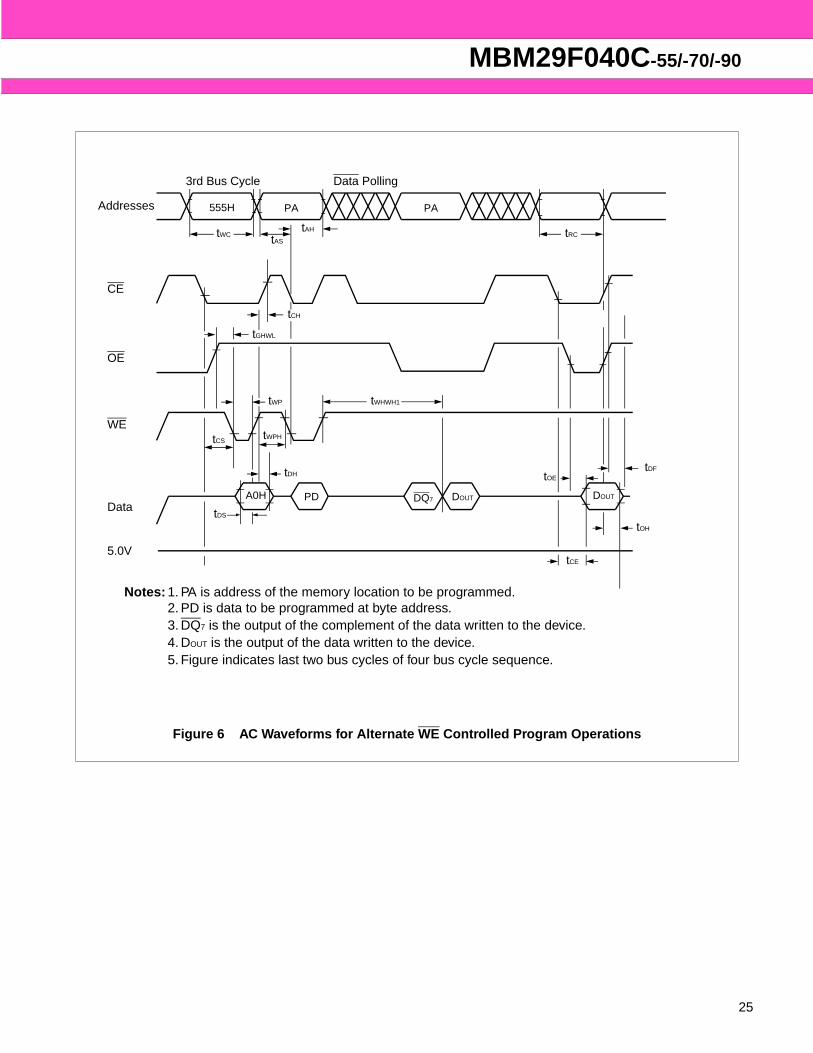
Figure 6 AC Waveforms for Alternate WE Controlled Program Operations
Notes: 1. PA is address of the memory location to be programmed.2. PD is data to be programmed at byte address.3. DQ7 is the output of the complement of the data written to the device.4. DOUT is the output of the data written to the device.5. Figure indicates last two bus cycles of four bus cycle sequence.
tGHWL
tWP
tDF
tDS
tWHWH1
tWCtAH
5.0V
CE
OE
tRC
Addresses
Data
tAS
tOE
tWPHtCS
tDH
DQ7PDA0H DOUT
tCE
WE
555H PA PA
tOH
Data Polling3rd Bus Cycle
tCH
DOUT
25

26
MBM29F040C-55/-70/-90
Figure 7 AC Waveforms for Alternate CE Controlled Program Operations
Notes: 1. PA is address of the memory location to be programmed.2. PD is data to be programmed at byte address.3. DQ7 is the output of the complement of the data written to the device.4. DOUT is the output of the data written to the device.5. Figure indicates last two bus cycles of four bus cycle sequence.
tGHEL
tCP
tDS
tWHWH1
tWCtAH
5.0V
WE
OE
Addresses
Data
tAS
tCPHtWS
tDH
DQ7PDA0H DOUT
CE
555H PA PA
Data Polling3rd Bus Cycle
tWH

MBM29F040C-55/-70/-90
Figure 8 AC Waveforms Chip/Sector Erase Operations
* : SA is the sector address for Sector Erase. Addresses = 555H for Chip Erase
tGHWL
tDS
V CC
CE
OE
Addresses
Data
tDH
WE
tAH
2AAH 555H555H 2AAH SA*
tWPHtCS
tWP
tVCS
tAS
555H
AAH 55H 80H AAH 55H 10H/30H
tCH
27

28
MBM29F040C-55/-70/-90
Figure 9 AC Waveforms for Data Polling during Embedded Algorithm Operations
* : DQ7 = Valid Data (The device has completed the Embedded operation.)
tOEH
tOE
tWHWH1 or 2
CE
OE
WE
t DF
tCH
tCE
High-ZDQ7 =Valid Data
DQ0 to DQ6 = Output Flag DQ0 to DQ6
tEOE
DQ7
High-ZValid Data
*
DQ7
DQ0 to DQ6 Data
Data
Figure 10 AC Waveforms for Toggle Bit I during Embedded Algorithm Operations
* : DQ6 stops toggling (The device has completed the Embedded operation).
tOEH
CE
WE
OE
DQ6
DQ6 = Toggle
*
tOES
tOE
DQ6 = ToggleDQ6 =
Stop TogglingDQ0 to DQ7
ValidData

MBM29F040C-55/-70/-90
Figure 11 AC Waveforms for Sector Protection Timing Diagram
tVLHT
SAX : Sector Address for initial sector
SAXA18
A17
A16
SAY
A0
A1
A9
VID
5V
tVLHT
OE
VID
5V
tVLHT
tOESP
tWPP
WE
CE
tOE
01HData
SAY : Sector Address for next sector
A6
A2 to A5
A7 to A18
tCSP
tVLHT
tVCS
VCC
29

30
MBM29F040C-55/-70/-90
Figure 12 DQ 2 vs. DQ6
Note: DQ2 is read from the erase-suspended sector.
DQ2
DQ6
WE Erase
EraseSuspend
EnterEmbedded
Erasing
Erase SuspendRead
Enter EraseSuspend Program
EraseSuspendProgram
Erase SuspendRead
EraseResume
Erase EraseComplete
ToggleDQ2 and DQ6
with OE

MBM29F040C-55/-70/-90
Figure 13 Embedded Program TM Algorithm
EMBEDDED ALGORITHMS
No
Yes
Program Command Sequence (Address/Command)
555H/AAH
2AAH/55H
555H/A0H
Write Program CommandSequence
(See below)
Data Polling Device
Increment Address Last Address?
Programming Completed
Program Address/Program Data
Start
31

32
MBM29F040C-55/-70/-90
Figure 4 Embedded Erase TM Algorithm
EMBEDDED ALGORITHMS
Start
555H/AAH
2AAH/55H
555H/AAH
555H/80H
555H/10H
2AAH/55H
555H/AAH
2AAH/55H
555H/AAH
555H/80H
2AAH/55H
Additional sectorerase commandsare optional.
Write Erase CommandSequece
(See below)
Data Polling or Toggle BitSuccessfully Completed
Erasure Completed
Chip Erase Command Sequence(Address/Command):
Individual Sector/Multiple SectorErase Command Sequence
(Address/Command):
Sector Address/30H
Sector Address/30H
Sector Address/30H

MBM29F040C-55/-70/-90
Figure 5 Data Polling Algorithm
Note: DQ7 is rechecked even if DQ5 = “1” because DQ7 may change simultaneously with DQ5.
VA = Byte address for programming= Any of the sector addresses within
the sector being erased duringsector erase or multiple sectorerases operation.
= Any of the sector addresses withinthe sector not being protectedduring sector erase or multiplesector erases operation.
Fail
DQ7 = Data?
No
No
DQ7 = Data?
DQ5 = 1?
Pass
Yes
Yes
Yes
No
Start
Read Byte(DQ0 to DQ7)
Addr. = VA
Read Byte(DQ0 to DQ7)
Addr. = VA
33

34
MBM29F040C-55/-70/-90
Figure 6 Toggle Bit Algorithm
Note: DQ6 is rechecked even if DQ5 = “1” because DQ6 may stop toggling at the same time as DQ5
changing to “1”.
Fail
DQ6 = Toggle?
Yes
No
DQ6 = Toggle
?
DQ5 = 1?
Pass
Yes
No
No
Yes
Start
Read Byte(DQ0 to DQ7)
Read Byte(DQ0 to DQ7)
Addr. = “H” or “L”
Addr. = “H” or “L”

MBM29F040C-55/-70/-90
Figure 7 Sector Protection Algorithm
Setup Sector Addr.(A18, A17, A16)
Activate WE Pulse
WE = VIH, CE = OE = VIL
(A9 should remain VID)
Yes
No
OE = VID, A9 = VID, CE = VIL
Time out 100 µs
Read from SectorAddr. = SA, A0 = 0, A1 = 1, A6 = 0
Remove VID from A9
Write Reset Command
Increment PLSCNT
No
Yes
Protect Another Sector ?
Start
Sector ProtectionCompleted
Data = 01H?
No
Yes
PLSCNT = 25?
Remove VID from A9
Write Reset Command
PLSCNT = 1
Device Failed
35

36
MBM29F040C-55/-70/-90
ERASE AND PROGRAMMING PERFORMANCE
TSOP(I) PIN CAPACITANCE
Note: Test conditions TA = 25°C, f = 1.0 MHz
PLCC PIN CAPACITANCE
Note: Test conditions TA = 25°C, f = 1.0 MHz
ParameterLimits
Unit CommentsMin. Typ. Max.
Sector Erase Time — 1 8 sec Excludes 00H programming prior to erasure
Byte Programming Time — 8 150 µs Excludes system-level overhead
Chip Programming Time — 4.2 10 sec Excludes system-level overhead
Erase/Program Cycle 100,000 — — cycles
Parameter Symbol Parameter Description Test Setup Typ. Max. Unit
CIN Input Capacitance VIN = 0 7 8 pF
COUT Output Capacitance VOUT = 0 8 10 pF
CIN2 Control Pin Capacitance VIN = 0 8.5 10 pF
Parameter Symbol Parameter Description Test Setup Typ. Max. Unit
CIN Input Capacitance VIN = 0 7 8 pF
COUT Output Capacitance VOUT = 0 8 10 pF
CIN2 Control Pin Capacitance VIN = 0 8.5 10 pF

MBM29F040C-55/-70/-90
PACKAGE DIMENSIONS
(Continued)
+0.05–0.02+.002–.001
INDEX
0.10(.004)
0.20
.008
(.410±.020)10.41±0.51
TYP0.66(.026)
TYP0.43(.017)
REF10.16(.400)
7.62(.300)REF
(.050±.005)1.27±0.13
TYPR0.95(.037)
(.510±.020)12.95±0.51
(.134±.006)3.40±0.16
(.089±.015)2.25±0.38
MIN0.64(.025)
(.588±.005)14.94±0.13
(.550±.003)13.97±0.08
(.487±.005)12.37±0.13
(.450±.003)11.43±0.08
14 20
29
2113
5
30324 1
1994 FUJITSU LIMITED C32021S-2C-4C Dimensions in mm(inches)
32-pin plastic QFJ(PLCC)(LCC-32P-M02)
37

38
MBM29F040C-55/-70/-90
(Continued)
+0.10–0.05
+.004–.002
0.25(.010)0.15(.006)
0.15(.006)MAX
0.35(.014)MAX
Details of "A" part
1.10 .043
(STAND OFF)0.05(.002)MIN
(.315±.008)8.00±0.20
TYP0.50(.0197)
0.10(.004) M
REF.7.50(.295)
(.008±.004)0.20±0.10
(.006±.002)0.15±0.05
(.020±.004)0.50±0.10
0.10(.004)
(.748±.008)19.00±0.20
(.724±.008)18.40±0.20(.787±.008)20.00±0.20
LEAD No.
"A"
INDEX
1716
321
1994 FUJITSU LIMITED F32035S-2C-1C
(Mounting Height)
Dimensions in mm(inches)
32-pin plastic TSOP(I)(FPT-32P-M24)

MBM29F040C-55/-70/-90
(Continued)
C 1997 FUJITSU LIMITED F32036S-2C-2
1 32
16 17
"A"
LEAD No.
19.00±0.20(.748±.008)
0.10(.004)
20.00±0.20(.787±.008)
18.40±0.20(.724±.008)
0.15±0.05(.006±.002)
0.50±0.10(.020±.004)
8.00±0.20(.315±.008)
7.50(.295)REF.
0.20±0.10(.008±.004)
0.50(.0197)TYP
M0.10(.004)
0.05(.002)MIN(STAND OFF)
.043 −.002+.004
−0.05+0.10
1.10
0.25(.010)0.15(.006)
0.15(.006)MAX
0.35(.014)MAX
Details of "A" part
INDEX
(Mounting Height)
Dimensions in mm(inches)
32-pin plastic TSOP(I)(FPT-32P-M25)
39

MBM29F040C-55/-70/-90
FUJITSU LIMITED
All Rights Reserved.
The contents of this document are subject to change without notice. Customers are advised to consult with FUJITSU salesrepresentatives before ordering.
The information and circuit diagrams in this document arepresented as examples of semiconductor device applications, andare not intended to be incorporated in devices for actual use. Also,FUJITSU is unable to assume responsibility for infringement ofany patent rights or other rights of third parties arising from the useof this information or circuit diagrams.
The products described in this document are designed, developedand manufactured as contemplated for general use, includingwithout limitation, ordinary industrial use, general office use,personal use, and household use, but are not designed, developedand manufactured as contemplated (1) for use accompanying fatalrisks or dangers that, unless extremely high safety is secured, couldhave a serious effect to the public, and could lead directly to death,personal injury, severe physical damage or other loss (i.e., nuclearreaction control in nuclear facility, aircraft flight control, air trafficcontrol, mass transport control, medical life support system, missilelaunch control in weapon system), or (2) for use requiringextremely high reliability (i.e., submersible repeater and artificialsatellite).Please note that Fujitsu will not be liable against you and/or anythird party for any claims or damages arising in connection withabove-mentioned uses of the products.
Any semiconductor devices have an inherent chance of failure. Youmust protect against injury, damage or loss from such failures byincorporating safety design measures into your facility andequipment such as redundancy, fire protection, and prevention ofover-current levels and other abnormal operating conditions.
If any products described in this document represent goods ortechnologies subject to certain restrictions on export under theForeign Exchange and Foreign Trade Law of Japan, the priorauthorization by Japanese government will be required for exportof those products from Japan.
F9903 FUJITSU LIMITED Printed in Japan