some numerical and experimental observa- … · x-band gunn oscillator b. c. sarkar1,*, c. koley1,...
TRANSCRIPT
Progress In Electromagnetics Research B, Vol. 40, 325–341, 2012
SOME NUMERICAL AND EXPERIMENTAL OBSERVA-TIONS ON THE GROWTH OF OSCILLATIONS IN ANX-BAND GUNN OSCILLATOR
B. C. Sarkar1, *, C. Koley1, A. K. Guin1, and S. Sarkar2
1Physics Department, Burdwan University, Burdwan 713104, India2Electronics Department, Burdwan Raj College, Burdwan 713104,India
Abstract—The dynamics of the onset of oscillations in a wave guidecavity based Gunn Oscillator (GO) has been critically examinedthrough numerical simulations and experimental studies. Thetransition of the GO from a non-oscillatory to an oscillatory state andthe same in the reverse direction occurs at different critical values ofthe dc bias voltage applied to the GO. In presence of a weak RF fieldin GO cavity, oscillations with broad band continuous spectrum andmultiple discrete line spectrum are observed at the GO output fordifferent values of dc bias below the above mentioned critical values.Analysing the numerically obtained time series data, chaos quantifiershave been obtained to prove the occurrence of the chaotic oscillations inthe GO. Experimental results and observations of numerical simulationshow good qualitative agreement.
1. INTRODUCTION
The physics of operation of a wave guide cavity based Gunn Oscillator(GO) has been studied at length during last fifty years since theinvention of the Gunn diode in the early sixties of the last century [1–6].A number of theoretical models for the GO have been proposed in theliterature to explain the obtained experimental observations regardingthe onset and the stabilization of oscillations in a GO [7–9]. It isestablished that when a Gunn diode is biased at a dc voltage above athreshold value, the negative differential resistance (NDR) of the diodecompensates the resistive component of the cavity impedance and thesystem breaks into self oscillation at a frequency determined by the
Received 28 March 2012, Accepted 28 April 2012, Scheduled 7 May 2012* Corresponding author: Bishnu Charan Sarkar (bcsarkar [email protected]).

326 Sarkar et al.
cavity and the device reactances [10]. In these studies the cavity isconsidered to be free from external RF field except those from thermalnoise.
Several other works have also been reported in the literaturedescribing and explaining the nonlinear dynamics of a GO [11, 12].It is well known that bifurcation and chaos are observed in a GOunder the influence of external periodic driving signals when the GOis operating in the normal active region [5, 15]. Some studies haveconsidered the presence of microwave frequency ac signals with the dcand thus obtained spatiotemporal chaos in the oscillator [14, 15]. Thesestudies are predominantly theoretical and concentrated on the physicalaspects of Gunn Effect. Further, to the knowledge of the authors, theeffect of gradual systematic increase of the dc bias in presence of RFfield in the GO cavity was not considered.
The present work intends to revisit the problem of onset ofoscillations in a GO when the oscillator cavity contains a weak externalRF field and the dc bias voltage (VB) is below the threshold value. Theeffect of the variation of frequency and power of the RF field presentwithin the cavity on the dynamics of the GO under such conditionsis also examined. It is shown by the numerical simulation and byexperimental studies that the under biased GO (i.e., a GO having VB
less than the threshold dc value for NDR region of operation) exhibitsdifferent dynamical states. They are respectively non oscillatory, quasiperiodic, chaotic and periodic oscillatory states depending upon thevalue of the dc bias.
The paper is organised in the following way. In Section 2,after brief description of the hardware structure of the GO, a circuittheoretic model of the system and differential equations describing thedynamics are given. The system equation can easily be identified asa modified Duffing oscillator equation with a term proportional tothe cube of the damping term. The dynamics of such a system ispotentially reach in nonlinear phenomenon (like chaos etc.) and wellstudied in the literature [13, 16–18]. However, the dynamics of a GOwith variable dc bias can be studied by this equation after propermodelling of the practical situation. The effect of the variation ofthe GO is taken into account by considering the variation of some ofthe device parameters in the oscillator model. These parameters aredependent on resistance and reactance of the diode. Section 3 describesthe results of numerical simulation. The obtained time series data setsare examined with the help of commercial Chaos Data Analyser (CDA)software for identification of different dynamical states of the system.Standard chaos quantifiers like maximal Lyapunov exponent (MLE)and correlation dimension (CD) are calculated. However no attempt

Progress In Electromagnetics Research B, Vol. 40, 2012 327
has been made to explain the route to chaos etc in this work. Theobtained results of the hardware experiment are reported in Section 4.They confirm the occurrence of chaotic, quasi periodic and periodicstates of the GO for different values of the applied dc voltage. Thepaper is concluded in Section 5 discussing the importance of the wholestudy.
2. CIRCUIT THEORETIC MODEL OF THEOSCILLATOR
From the knowledge of the operation of a Gunn diode, biased at theactive region, it can be modelled by a parallel or series combination oftwo voltage dependent nonlinear circuit elements — one resistive andthe other capacitive in nature. As the applied dc voltage across thediode crosses the threshold value it operates in NDR region and thevalue of this NDR is a function of the magnitude of VB. Therefore,the relation between the incremental current (i) through the diodeand the incremental voltage (vr) across the diode is a nonlinear one.Considering the nonlinearity as cubic type, one writes it as
vr = −β1i + β3i3 (1)
Here, β1 and β3 are the parameters taking care of linear andnonlinear dependence between the voltage and the current. Theirmagnitudes are determined by the value of the applied VB. Abovethe threshold value β1 is negative. The diode capacitance in the acmodel is taken as voltage dependent due to the modification of theeffective dielectric constant of the diode material in the presence of thenegative charge in the active condition [8]. Thus one can write theinstantaneous voltage (vc) across the equivalent capacitor in terms ofthe instantaneous charge (q =
∫i · dt) as
vc = −α1q + α3q3 (2)
Here α1 and α3 are the parameters taking care of linear and nonlinearcomponents of diode capacitance. Thus the Gunn diode is replaced bya series combination of two nonlinear voltage sources vr and vc whenan instantaneous current i(= dq
dt ) passes through it. The wave guidetype cavity is replaced by a series combination of inductor L, capacitorC and the resistor R. This R takes care of the cavity loss and the loadresistor. Figure 1 shows the ac circuit theoretic model, of the GO. Thevoltage source vs indicated in Figure 1 represents the presence of theexternal field within the cavity. It is replaced by a short circuit whenthere would be no external field present other than the noise voltagedue to the finite temperature in the cavity.

328 Sarkar et al.
Figure 1. Series equivalent circuit of the Gunn Oscillator.
The differential equation describing the dynamics of the system isderived from the model depicted in Figure 1 applying the Kirchhoff’smesh law. The obtained equation is written as follows after somelogical substitution and normalization [19]:
d2q
dτ2= aq − bq3 + c
dq
dτ− d
(dq
dτ
)3
+ qs cos(Ωτ) (3)
Here dqdt = i is the instantaneous circulating current and τ(= ωrt)
is the normalized time. ωr(= 1√LC
) represents the resonant frequencyof the cavity. qs and Ω are respectively the charge equivalent to theamplitude and the normalized angular frequency of the external fieldpresent within the cavity. The coefficients a, b, c and d are relatedwith the resistive and the reactive parts of the device and the cavityimpedances as follows:
a = α1C − 1 (4)b = α3C (5)
c =β1 −R−RL
ωrL(6)
d =β3ωr
L(7)
It is evident the coefficients a, b, c and d are implicitly dependenton the magnitude of VB through bias dependent parameters β1, β3,α1 and α3. Since α1 and α3 are related to the capacitive parameters,their values determines the oscillation frequency. As β1 and β3 are
Progress In Electromagnetics Research B, Vol. 40, 2012 329
related to the device resistance so they demand more attention in theanalysis of onset of oscillation. Also the relative magnitude of β3 ismuch less compared to β1, hence the parameter d can be taken smallerthan c. The effect of variation of the applied dc bias would be studiedby considering the variation of c. Note that the increase in the valueof VB results in the decrease in the value of c [19].
3. NUMERICAL ANALYSIS
It is difficult, if not impossible, to get a general closed form solutionof (3). So a numerical solution of it is obtained in the following way.We introduce a new state variable p and write:
dq
dτ= p (8)
dp
dτ= aq − bq3 + cp− dp3 + qs cos(Ωτ) (9)
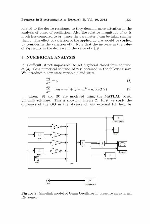
Then, (8) and (9) are modelled using the MATLAB basedSimulink software. This is shown in Figure 2. First we study thedynamics of the GO in the absence of any external RF field by
Figure 2. Simulink model of Gunn Oscillator in presence an externalRF source.

330 Sarkar et al.
Figure 3. c-d parameter space plot to see non oscillatory (blue color)and stable oscillatory (red color) region of the free running GunnOscillator (a = 1, b = 1).
disconnecting the sinusoidal source from the Simulink model of GO.Considering a = 1 and b = 1, we take different pairs of values for cand d and perform the simulation to find the dynamical state of thesystem. The obtained state is either oscillatory or non-oscillatory innature. Figure 3 shows the parameter space involving c and d resultinginto these two states. Using Figure 3 the steady state values of q andp are obtained for a particular set of values of a, b, c and d. Thesevalues of q and p are taken as initial values for the next simulation withincreased (decreased) value of c. We take a = 1, b = 1, d = 0.015 andexamine the effect of the variation of c. As c decreases gradually from0.06 the system begins to oscillate at c = −0.06. With these parametervalues, the normalized frequency and amplitude of the free running GOare calculated as 1.27 and 2.0 respectively. Then, increasing the valueof c from −0.06 the quenching of oscillation is obtained at c = 0.01.These two different values of indicate the occurrence of ‘hysteresis’phenomenon in the onset and quenching of oscillation in a GO as afunction of the dc bias voltage.
The effect of the external RF field is examined by considering theadditional term qs cos(Ωτ) in (9). With a = 1, b = 1, d = 0.015 asbefore, we take qs and Ω as 0.15 and 1.27 respectively (This ensuresthe presence of a weak RF field of frequency close to the free runningfrequency of the GO in the cavity). Then we repeat the numerical
Progress In Electromagnetics Research B, Vol. 40, 2012 331
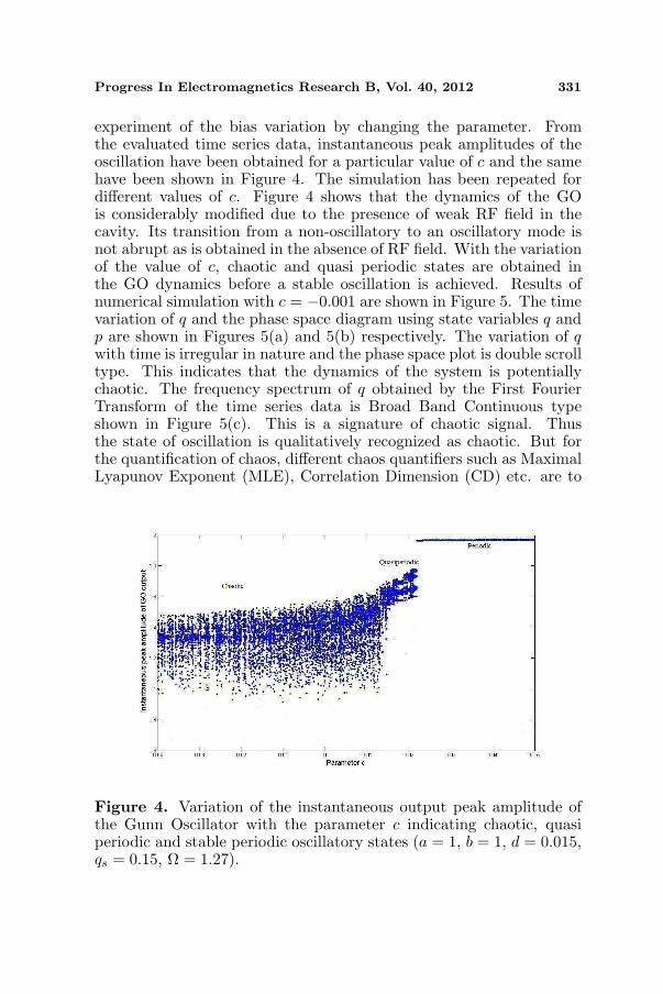
experiment of the bias variation by changing the parameter. Fromthe evaluated time series data, instantaneous peak amplitudes of theoscillation have been obtained for a particular value of c and the samehave been shown in Figure 4. The simulation has been repeated fordifferent values of c. Figure 4 shows that the dynamics of the GOis considerably modified due to the presence of weak RF field in thecavity. Its transition from a non-oscillatory to an oscillatory mode isnot abrupt as is obtained in the absence of RF field. With the variationof the value of c, chaotic and quasi periodic states are obtained inthe GO dynamics before a stable oscillation is achieved. Results ofnumerical simulation with c = −0.001 are shown in Figure 5. The timevariation of q and the phase space diagram using state variables q andp are shown in Figures 5(a) and 5(b) respectively. The variation of qwith time is irregular in nature and the phase space plot is double scrolltype. This indicates that the dynamics of the system is potentiallychaotic. The frequency spectrum of q obtained by the First FourierTransform of the time series data is Broad Band Continuous typeshown in Figure 5(c). This is a signature of chaotic signal. Thusthe state of oscillation is qualitatively recognized as chaotic. But forthe quantification of chaos, different chaos quantifiers such as MaximalLyapunov Exponent (MLE), Correlation Dimension (CD) etc. are to
Figure 4. Variation of the instantaneous output peak amplitude ofthe Gunn Oscillator with the parameter c indicating chaotic, quasiperiodic and stable periodic oscillatory states (a = 1, b = 1, d = 0.015,qs = 0.15, Ω = 1.27).
332 Sarkar et al.
(a) (b) (c)
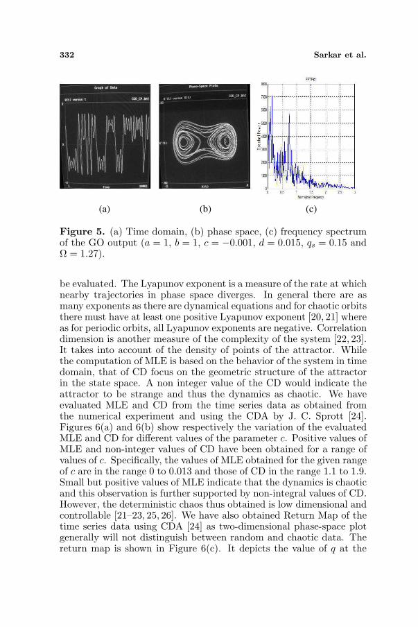
Figure 5. (a) Time domain, (b) phase space, (c) frequency spectrumof the GO output (a = 1, b = 1, c = −0.001, d = 0.015, qs = 0.15 andΩ = 1.27).
be evaluated. The Lyapunov exponent is a measure of the rate at whichnearby trajectories in phase space diverges. In general there are asmany exponents as there are dynamical equations and for chaotic orbitsthere must have at least one positive Lyapunov exponent [20, 21] whereas for periodic orbits, all Lyapunov exponents are negative. Correlationdimension is another measure of the complexity of the system [22, 23].It takes into account of the density of points of the attractor. Whilethe computation of MLE is based on the behavior of the system in timedomain, that of CD focus on the geometric structure of the attractorin the state space. A non integer value of the CD would indicate theattractor to be strange and thus the dynamics as chaotic. We haveevaluated MLE and CD from the time series data as obtained fromthe numerical experiment and using the CDA by J. C. Sprott [24].Figures 6(a) and 6(b) show respectively the variation of the evaluatedMLE and CD for different values of the parameter c. Positive values ofMLE and non-integer values of CD have been obtained for a range ofvalues of c. Specifically, the values of MLE obtained for the given rangeof c are in the range 0 to 0.013 and those of CD in the range 1.1 to 1.9.Small but positive values of MLE indicate that the dynamics is chaoticand this observation is further supported by non-integral values of CD.However, the deterministic chaos thus obtained is low dimensional andcontrollable [21–23, 25, 26]. We have also obtained Return Map of thetime series data using CDA [24] as two-dimensional phase-space plotgenerally will not distinguish between random and chaotic data. Thereturn map is shown in Figure 6(c). It depicts the value of q at the

Progress In Electromagnetics Research B, Vol. 40, 2012 333
time when p equals a constant versus the value of q at the previoustime at which p equalled the same constant. The obtained return mapindicates the chaotic dynamics of the system for the selected set of thetime series data.
In order to study how the frequency of the weak RF field affectsthe dynamics of the under biased GO, numerical simulation has beendone by taking the values of the parameters a, b and d as beforewith c = −0.001, and then varying Ω. Figure 7 shows variation of
(a) (b) (c)
Figure 6. Variation of (a) MLE, (b) CD with the parameter c, (c)return map of the time series data (a = 1, b = 1, c = −0.001, d = 0.015,qs = 0.15 and Ω = 1.27).
(a) (b) (c)
Figure 7. Frequency spectra of the GO output (a) Ω = 1.256, (b)Ω = 1.269, (c) Ω = 1.279 (a = 1, b = 1, c = −0.001, d = 0.015 andqs = 0.15).
334 Sarkar et al.
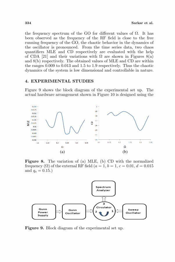
the frequency spectrum of the GO for different values of Ω. It hasbeen observed as the frequency of the RF field is close to the freerunning frequency of the GO, the chaotic behavior in the dynamics ofthe oscillator is pronounced. From the time series data, two chaosquantifiers MLE and CD respectively are evaluated with the helpof CDA [21] and their variations with Ω are shown in Figures 8(a)and 8(b) respectively. The obtained values of MLE and CD are withinthe ranges 0.009 to 0.013 and 1.5 to 1.9 respectively. Thus the chaoticdynamics of the system is low dimensional and controllable in nature.
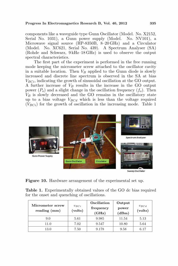
4. EXPERIMENTAL STUDIES
Figure 9 shows the block diagram of the experimental set up. Theactual hardware arrangement shown in Figure 10 is designed using the
(a) (b)
Figure 8. The variation of (a) MLE, (b) CD with the normalizedfrequency (Ω) of the external RF field (a = 1, b = 1, c = 0.01, d = 0.015and qs = 0.15.)
Figure 9. Block diagram of the experimental set up.
Progress In Electromagnetics Research B, Vol. 40, 2012 335
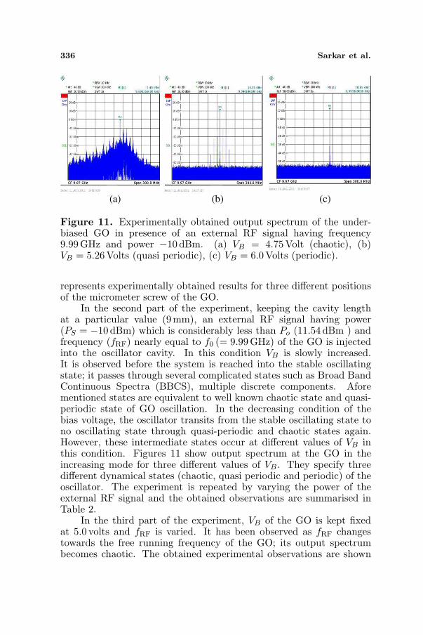
components like a waveguide type Gunn Oscillator (Model. No. X2152,Serial No. 1031), a Gunn power supply (Model. No. NV101), aMicrowave signal source (HP-8350B, 8–20 GHz) and a Circulator(Model. No. XC621, Serial No. 439). A Spectrum Analyser (SA)(Rohde and Schwarz, 9 kHz–18GHz) is used to observe the outputspectral characteristics.
The first part of the experiment is performed in the free runningmode keeping the micrometer screw attached to the oscillator cavityin a suitable location. Then VB applied to the Gunn diode is slowlyincreased and discrete line spectrum is observed in the SA at biasVBCi, indicating the growth of sinusoidal oscillation at the GO output.A further increase of VB results in the increase in the GO outputpower (Po) and a slight change in the oscillation frequency (fo). ThenVB is slowly decreased and the GO remains in the oscillatory stateup to a bias voltage VBCd which is less than the voltage required(VBCi) for the growth of oscillation in the increasing mode. Table 1
Figure 10. Hardware arrangement of the experimental set up.
Table 1. Experimentally obtained values of the GO dc bias requiredfor the onset and quenching of oscillations.
Micrometer screw
reading (mm)
vBCi
(volts)
Oscillation
frequency
(GHz)
Output
power
(dBm)
vBCd
(volts)
9.0 5.61 9.985 11.54 5.13
11.0 7.02 9.547 10.80 5.64
13.0 7.50 9.178 9.58 6.17
336 Sarkar et al.
(a) (b) (c)
Figure 11. Experimentally obtained output spectrum of the under-biased GO in presence of an external RF signal having frequency9.99GHz and power −10 dBm. (a) VB = 4.75Volt (chaotic), (b)VB = 5.26Volts (quasi periodic), (c) VB = 6.0 Volts (periodic).
represents experimentally obtained results for three different positionsof the micrometer screw of the GO.
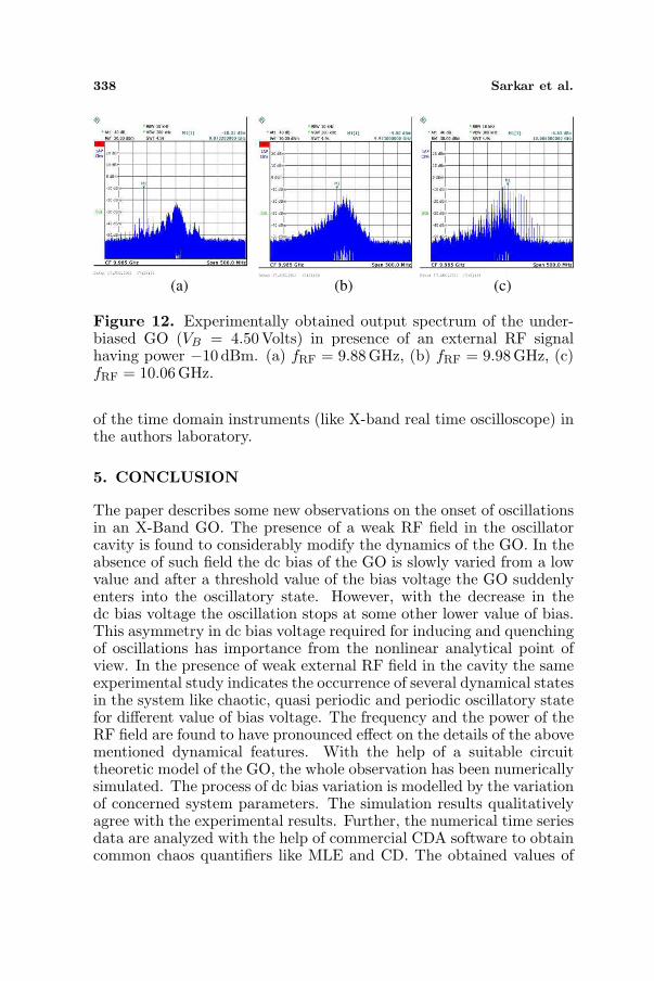
In the second part of the experiment, keeping the cavity lengthat a particular value (9 mm), an external RF signal having power(PS = −10 dBm) which is considerably less than Po (11.54 dBm ) andfrequency (fRF) nearly equal to f0 (= 9.99GHz) of the GO is injectedinto the oscillator cavity. In this condition VB is slowly increased.It is observed before the system is reached into the stable oscillatingstate; it passes through several complicated states such as Broad BandContinuous Spectra (BBCS), multiple discrete components. Aforementioned states are equivalent to well known chaotic state and quasi-periodic state of GO oscillation. In the decreasing condition of thebias voltage, the oscillator transits from the stable oscillating state tono oscillating state through quasi-periodic and chaotic states again.However, these intermediate states occur at different values of VB inthis condition. Figures 11 show output spectrum at the GO in theincreasing mode for three different values of VB. They specify threedifferent dynamical states (chaotic, quasi periodic and periodic) of theoscillator. The experiment is repeated by varying the power of theexternal RF signal and the obtained observations are summarised inTable 2.
In the third part of the experiment, VB of the GO is kept fixedat 5.0 volts and fRF is varied. It has been observed as fRF changestowards the free running frequency of the GO; its output spectrumbecomes chaotic. The obtained experimental observations are shown

Progress In Electromagnetics Research B, Vol. 40, 2012 337
Table 2. Experimental observations on the nature of the GO outputspectrum for different values of the GO dc bias with a fixed powerinjected field in the GO cavity.
Ps
(dBm)
VB
(Volts)Nature of the output spectrum of the GO
−20
3.2 Non Oscillatory
3.34BBCS having peak power (Ppeak = −30 dBm) 10 dBm
Bandwidth (BW = 80 MHz)
3.42 BBCS having Ppeak = −40 dBm and BW = 60 MHz
3.5 BBCS having Ppeak = −45 dBm and BW = 50 MHz
5.4
Quasi-Periodic having components 9.975GHz
(−45 dBm), 9.98 GHz (−15 dBm), 9.985GHz (10.31 dBm),
9.90GHz (−15 dBm), 9.95 GHz (−48 dBm)
5.92 Periodic having frequency 9.99GHz and power 10.76 dBm
−10
3.3 Non Oscillatory
3.9BBCS having peak power (Ppeak = −30 dBm)
BW = 90 MHz
4.1 BBCS having Ppeak = −25 dBm and BW = 90 MHz
4.75 BBCS having Ppeak = −22 dBm and BW = 120 MHz
5.0 BBCS having Ppeak = −20 dBm and BW = 100 MHz
5.26
Quasi-Periodic having components 9.95GHz (−40 dBm),
9.96GHz (−30 dBm), 9.97 GHz (−20 dBm),
9.98GHz (10.06 dBm), 9.99 GHz (−10 dBm),
10.0GHz (−15 dBm),10.01 GHz (−35 dBm)
6 Periodic having frequency 9.99GHz and power 10.85 dBm
in Figure 12 for three different values of fRF. They indicate theaverage power and bandwidth of the chaotic spectrum increases as fRF
becomes close to f0. It has to be mentioned here that the generationof chaotic oscillations at the GO output is very much predictable fora particular arrangement of the GO circuit. The dc bias has to beadjusted slightly below the threshold bias required for the periodicoscillations and injected RF field frequency should be around resonantfrequency of the cavity. The system can be used as a generatorof robust deterministic chaos of low average power at the frequencyrange 9GHz to 10 GHz. In the literature, one can find microwavefrequency chaos generators using different forms of active circuits likecolpitts oscillators, CMOS structure, phase locked loop etc. [27–31].The quantification of the experimentally generated chaos in the GObased circuit could not be done here because of the non availability
338 Sarkar et al.
(a) (b) (c)
Figure 12. Experimentally obtained output spectrum of the under-biased GO (VB = 4.50Volts) in presence of an external RF signalhaving power −10 dBm. (a) fRF = 9.88GHz, (b) fRF = 9.98GHz, (c)fRF = 10.06GHz.
of the time domain instruments (like X-band real time oscilloscope) inthe authors laboratory.
5. CONCLUSION
The paper describes some new observations on the onset of oscillationsin an X-Band GO. The presence of a weak RF field in the oscillatorcavity is found to considerably modify the dynamics of the GO. In theabsence of such field the dc bias of the GO is slowly varied from a lowvalue and after a threshold value of the bias voltage the GO suddenlyenters into the oscillatory state. However, with the decrease in thedc bias voltage the oscillation stops at some other lower value of bias.This asymmetry in dc bias voltage required for inducing and quenchingof oscillations has importance from the nonlinear analytical point ofview. In the presence of weak external RF field in the cavity the sameexperimental study indicates the occurrence of several dynamical statesin the system like chaotic, quasi periodic and periodic oscillatory statefor different value of bias voltage. The frequency and the power of theRF field are found to have pronounced effect on the details of the abovementioned dynamical features. With the help of a suitable circuittheoretic model of the GO, the whole observation has been numericallysimulated. The process of dc bias variation is modelled by the variationof concerned system parameters. The simulation results qualitativelyagree with the experimental results. Further, the numerical time seriesdata are analyzed with the help of commercial CDA software to obtaincommon chaos quantifiers like MLE and CD. The obtained values of
Progress In Electromagnetics Research B, Vol. 40, 2012 339
these parameters confirm the chaotic dynamics of the GO. This studyreported here additionally suggests a convenient method of generationof chaotic oscillation in an X-Band GO. The applied dc bias voltagebelow the threshold value and the external RF field to be applied in GOcavity could be the suitable control parameters of such chaos generator.This said system would have potential application in microwave chaoticcommunications.
ACKNOWLEDGMENT
Authors acknowledge partial financial assistance from DAE, BRNS(India) and DST (India) through sponsored research projects incarrying out the work.
REFERENCES
1. Kurokawa, K., “Injection locking of microwave solid stateoscillator,” Proc. IEEE , Vol. 61, 1386–1410, 1973.
2. Ito, Y., et al., “Cavity stabilized X-band Gunn Oscillator,” IEEETransactions on Microwave Theory and Techniques, Vol. 18, 870–897, 1970.
3. Holtzman, E. L. and R. S. Robertson, Solid State MicrowavePower Oscillator Design, Chapters 2, 4 and 7, Artech House,Norwood, MA, 1992.
4. Solano, M. A., J. S. Ipina, J. M. Zamanillo, and C. P. Vega, “X-band Gunn diode oscillator for a multiple frequency continuous-wave radar for educational purposes,” IEEE Transactions onEducation, Vol. 45, 316–322, 2002.
5. Chakravorty, J., T. Banerjee, R. Ghatak, A. Bose, andB. C. Sarkar, “Generating chaos in injection-synchronized GunnOscillator: An experimental approach,” IETE Journal ofResearch, Vol. 55, 106–111, 2009.
6. Ko, D. S., S. J. Lee, T. J. Baek, S. G. Choi, M. Han, H. C. Park,J. K. Rhee, J. H. Jung, and Y. W. Park, “New tuning method for94GHz waveguide voltage controlled oscillator,” IEEE Microwaveand Wireless Components Letters, Vol. 21, No. 3, Mar. 2011.
7. Kao, C. H. and L. W. Chen, “A hydrodynamic equivalent circuitmodel for the Gunn diode,” Solid-State Electronics, Vol. 46, 915–923, 2002.
8. Pence, I. W. and P. J. Khan, “Broad band equivalent circuitdetermination of Gunn diodes,” IEEE Transactions on MicrowaveTheory and Techniques, Vol. 18, No. 11, Nov. 1970.

340 Sarkar et al.
9. Shalatonin, V., “Modeling of the nonlinear dynamics in a Gunnchaos oscillator,” 18th Int. Crimean Conference in Microwaveand Telecommunication Technology, Sevatopol, Crimea, Ukraine,Sep. 8–12, 2008.
10. Hakki, B. W., “Amplification in two valley semiconductors,” J.Applied Physics, Vol. 38, No. 2, 808–818, Feb. 1967.
11. Shiau, Y. H., “Stochastic resonance in the Gunn effect,” PhysicsRev. B , Vol. 60, No. 23, 15534–15537.
12. Mosekilde, E., et al., “Phase diagram for periodically driven Gunndiode,” Physica D , Vol. 66, 143–153, 1993.
13. Lakshmanan, M. and S. Rajsekar, Non Linear Dynamics,Integrability, Chaos and Patterns, Springer, 2003.
14. Shiau, Y. H. and Y. C. Cheng, “Hybrid electric field domainsleading to spatiotemporal chaos in N-GaAs,” Physical Rev. B ,Vol. 56, No. 15, 9247–9250, Oct. 1997.
15. Mosekilde, E., et al., “Mode locking and spatio-temporal chaos inperiodically driven Gunn diode,” Physical Rev. B , Vol. 41, 2298–2306, 1990.
16. Kao, Y. H., J. C. Huang, and Y. S. Gou, “Routes to chaos induffing oscillator with one potential well,” IEEE InternationalSymposium, Vol. 1, 265–268, 1988.
17. Novak, S. and R. G. Frehlich, “Transition to chaos in the duffingoscillator,” Phys. Rev. A, Vol. 26, 3660–3663, 1982.
18. Musielak, D. E., Z. E. Musielak, and J. W. Banner, “Chaos androute to chaos in coupled duffing oscillators with multiple degreeof freedom,” Science Direct , Vol. 24, 907–922, 2005.
19. Sarkar, B. C., D. Sarkar, S. Sarkar, and J. Chakraborty, “Studieson the dynamics of bilaterally coupled X-band Gunn oscillators,”Progress In Electromagnetics Research B , Vol. 32, 149–167, 2011.
20. Jordan, D. W. and P. Smith, Nonlinear Ordinary DifferentialEquations; An Introduction for Scientists and Engineers, 4thEdition, Oxford University Press, 2009.
21. Hilborn, R. C., Chaos and Non Linear Dynamics, OxfordUniversity Press, 2000.
22. Sprott, J. C., Chaos and Time Series Analysis, Oxford UniversityPress, 2003.
23. Strogatz, S. H., Nonlinear Dynamics and Chaos, West View Press,2007.
24. Sprott, J. C., Chaos Data Analyzer Package, Web address:http://sprott.physics.wisc.edu/cda.htm.
Progress In Electromagnetics Research B, Vol. 40, 2012 341
25. Ram, R. J., R. Sporer, H.-R. Blank, and R. A. York, “Chaoticdynamics in coupled microwave oscillators,” IEEE Transactionson Microwave Theory and Techniques, Vol. 48, No. 11, 1909–1916,2000.
26. Bulashenko, O. M., M. J. Garcia, and L. L. Bonilla,“Chaotic dynamics of electric-field domains in periodically drivensuperlattices,” Physical Rev. B , Vol. 53, No. 15, 10008–10018,1996.
27. Shi, Z. G. and L. X. Ran, “Microwave chaotic Colpittsoscillator: Design, implementation and applications,” Journal ofElectromagnetic Waves and Applications, Vol. 20, No. 10, 1335–1349, 2006.
28. Stefanidis, V., O. Tsakiridis, E. Zervas, and J. Stonham, “Designof a microwave chaotic oscillator using symmetric active load,”Latest Trends on Circuit , 2010.
29. Jiang, T., S. Qiao, Z.-G. Shi, L. Peng, J. Huangfu, W.-Z. Cui,W. Ma, and L.-X. Ran, “Simulation and experimental evaluationof the radar signal performance of chaotic signals generated froma microwave Colpitts oscillator,” Progress In ElectromagneticsResearch, Vol. 90, 15–30, 2009.
30. Nikishov, A. Y., “Generation of the microwave chaotic oscillationsby CMOS structure,” PIERS Proceedings, 457–461, Moscow,Russia, Aug. 18–21, 2009.
31. Dmitriev, A. S., A. V. Kletsov, and L. V. Kuzmin, “Experimentalgeneration of chaotic oscillations in microwave band by phase-locked loop,” PIERS Proceedings, 1498–1502, Moscow, Russia,Aug. 18–21, 2009.