solvent annealing of perovskite ... articles/2014-11 solvent... · solvent annealing of...
TRANSCRIPT
© 2014 WILEY-VCH Verlag GmbH & Co. KGaA, Weinheim 6503wileyonlinelibrary.com
CO
MM
UN
ICATIO
N
Solvent Annealing of Perovskite-Induced Crystal Growth for Photovoltaic-Device Effi ciency Enhancement
Zhengguo Xiao , Qingfeng Dong , Cheng Bi , Yuchuan Shao , Yongbo Yuan , and Jinsong Huang*
Z. Xiao, Dr. Q. Dong, C. Bi, Y. Shao, Dr. Y. Yuan, Prof. J. Huang Department of Mechanical and Materials Engineering and Nebraska Center for Materials and Nanoscience University of Nebraska-Lincoln Lincoln , NE 68588–0526, USA E-mail: [email protected]
DOI: 10.1002/adma.201401685
the margin is very small, as shown in this work. Moreover, high-temperature thermal annealing, or even low-temperature thermal annealing for long periods, decomposes the perovskite fi lms and so decreases the device effi ciency. [ 22,23 ]
In this manuscript, we report that solvent annealing effec-tively increases the crystallinity and grain size of CH 3 NH 3 PbI 3 fi lm. The average grain size of the solvent-annealed trihalide CH 3 NH 3 PbI 3 fi lms increased to 1 µm, which is comparable to the fi lm thickness, while the maximum grain size in thermal annealed fi lms was only around 260 nm. Solvent annealing dra-matically improved the electronic properties of the perovskite fi lms. The best-performing device with planar structure had an effi ciency of 15.6% under air mass global (AM 1.5G) spec-trum illumination with a perovskite thickness of 630 nm; the effi ciency dropped only slightly to 14.5% when the pervoskite thickness increased to 1 µm.
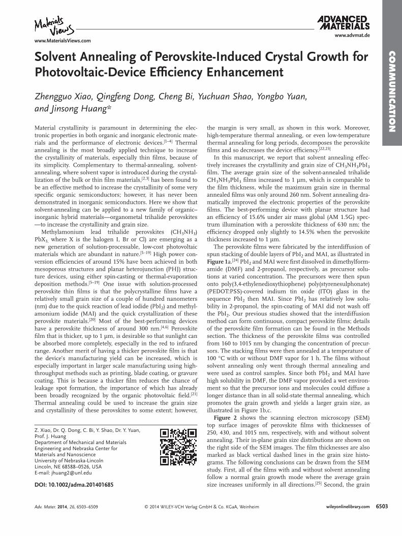
The perovskite fi lms were fabricated by the interdiffusion of spun stacking of double layers of PbI 2 and MAI, as illustrated in Figure 1 a. [ 24 ] PbI 2 and MAI were fi rst dissolved in dimethylform-amide (DMF) and 2-propanol, respectively, as precursor solu-tions at varied concentration. The precursors were then spun onto poly(3,4-ethylenedioxythiophene) poly(styrenesulphonate) (PEDOT:PSS)-covered indium tin oxide (ITO) glass in the sequence PbI 2 then MAI. Since PbI 2 has relatively low solu-bility in 2-propanol, the spin-coating of MAI did not wash off the PbI 2 . Our previous studies showed that the interdiffusion method can form continuous, compact perovskite fi lms; details of the perovskite fi lm formation can be found in the Methods section. The thickness of the perovskite fi lms was controlled from 160 to 1015 nm by changing the concentration of precur-sors. The stacking fi lms were then annealed at a temperature of 100 °C with or without DMF vapor for 1 h. The fi lms without solvent annealing only went through thermal annealing and were used as control samples. Since both PbI 2 and MAI have high solubility in DMF, the DMF vapor provided a wet environ-ment so that the precursor ions and molecules could diffuse a longer distance than in all solid-state thermal annealing, which promotes the grain growth and yields a larger grain size, as illustrated in Figure 1 b,c.
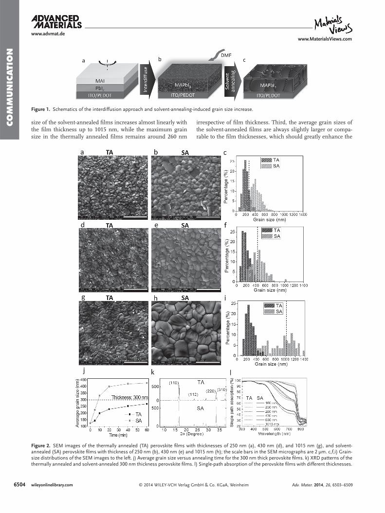
Figure 2 shows the scanning electron microscopy (SEM) top surface images of perovskite fi lms with thicknesses of 250, 430, and 1015 nm, respectively, with and without solvent annealing. Their in-plane grain size distributions are shown on the right side of the SEM images. The fi lm thicknesses are also marked as black vertical dashed lines in the grain size histo-grams. The following conclusions can be drawn from the SEM study. First, all of the fi lms with and without solvent annealing follow a normal grain growth mode where the average grain size increases uniformly in all directions. [ 25 ] Second, the grain
Material crystallinity is paramount in determining the elec-tronic properties in both organic and inorganic electronic mate-rials and the performance of electronic devices. [ 1–4 ] Thermal annealing is the most broadly applied technique to increase the crystallinity of materials, especially thin fi lms, because of its simplicity. Complementary to thermal-annealing, solvent-annealing, where solvent vapor is introduced during the crystal-lization of the bulk or thin fi lm materials, [ 2,3 ] has been found to be an effective method to increase the crystallinity of some very specifi c organic semiconductors; however, it has never been demonstrated in inorganic semiconductors. Here we show that solvent-annealing can be applied to a new family of organic–inorganic hybrid materials—organometal trihalide perovskites —to increase the crystallinity and grain size.
Methylamonium lead trihalide perovskites (CH 3 NH 3 )PbX 3, where X is the halogen I, Br or Cl) are emerging as a new generation of solution-processable, low-cost photovoltaic materials which are abundant in nature. [ 5–19 ] High power con-version effi ciencies of around 15% have been achieved in both mesoporous structures and planar heterojunction (PHJ) struc-ture devices, using either spin-casting or thermal-evaporation deposition methods. [ 5–19 ] One issue with solution-processed perovskite thin fi lms is that the polycrystalline fi lms have a relatively small grain size of a couple of hundred nanometers (nm) due to the quick reaction of lead iodide (PbI 2 ) and methyl-amonium iodide (MAI) and the quick crystallization of these perovskite materials. [ 20 ] Most of the best-performing devices have a perovskite thickness of around 300 nm. [ 4,6 ] Perovskite fi lm that is thicker, up to 1 µm, is desirable so that sunlight can be absorbed more completely, especially in the red to infrared range. Another merit of having a thicker perovskite fi lm is that the device’s manufacturing yield can be increased, which is especially important in larger scale manufacturing using high-throughput methods such as printing, blade coating, or gravure coating. This is because a thicker fi lm reduces the chance of leakage spot formation, the importance of which has already been broadly recognized by the organic photovoltaic fi eld. [ 21 ] Thermal annealing could be used to increase the grain size and crystallinity of these perovskites to some extent; however,
Adv. Mater. 2014, 26, 6503–6509
www.advmat.dewww.MaterialsViews.com
6504 wileyonlinelibrary.com © 2014 WILEY-VCH Verlag GmbH & Co. KGaA, Weinheim
CO
MM
UN
ICATI
ON
size of the solvent-annealed fi lms increases almost linearly with the fi lm thickness up to 1015 nm, while the maximum grain size in the thermally annealed fi lms remains around 260 nm
irrespective of fi lm thickness. Third, the average grain sizes of the solvent-annealed fi lms are always slightly larger or compa-rable to the fi lm thicknesses, which should greatly enhance the
Adv. Mater. 2014, 26, 6503–6509
www.advmat.dewww.MaterialsViews.com
Figure 1. Schematics of the interdiffusion approach and solvent-annealing-induced grain size increase.
Figure 2. SEM images of the thermally annealed (TA) perovskite fi lms with thicknesses of 250 nm (a), 430 nm (d), and 1015 nm (g), and solvent-annealed (SA) perovskite fi lms with thickness of 250 nm (b), 430 nm (e) and 1015 nm (h); the scale bars in the SEM micrographs are 2 µm. c,f,i) Grain-size distributions of the SEM images to the left. j) Average grain size versus annealing time for the 300 nm thick perovskite fi lms. k) XRD patterns of the thermally annealed and solvent-annealed 300 nm thickness perovskite fi lms. l) Single-path absorption of the perovskite fi lms with different thicknesses.
6505wileyonlinelibrary.com© 2014 WILEY-VCH Verlag GmbH & Co. KGaA, Weinheim
CO
MM
UN
ICATIO
N
charge extraction process; this is because the photogenerated charges do not need to go through any grain boundaries during their transport in the out-of-plane direction before being collected by the electrodes.
The dynamic grain growth process of thermal annealing and solvent annealing of a 300 nm thick perovskite fi lms was studied by varying thermal and solvent annealing time from 0 to 60 min. The SEM surface images are shown in Figure S1 in the Sup-porting Information. The average grain size versus time is summarized in Figure 2 j. Due to the quick reaction of PbI 2 and MAI and quick crystallization of MAPbI 3 , the as-pre-pared perovskite fi lms were polycrystalline with a small average grain size of 125 nm. The grain size of both thermally annealed and solvent-annealed fi lms grew with increased annealing time. The grain size increase was fast in the fi rst 20 min, and then slowed down and saturated with fur-ther annealing. The grain size of the solvent-annealed fi lm grew much faster than the thermally annealed fi lms: solvent-annealing for 20 min increased the average grain size to 400 nm, which was already larger than the fi lm thickness, while thermal-annealing for 60 min only increased the grain size to 260 nm, smaller than the fi lm thickness.
The solvent annealing-induced crystallinity change was measured by X-ray diffraction (XRD). Figure 2 k shows the XRD results of the solvent-annealed and thermally annealed 300 nm thick perovskite fi lms. All of the XRD diffraction peaks of the solvent-annealed fi lms were sharper than those of the thermal-annealed fi lms, which indicates increased crystallinity with fewer low-dimensional defects and/or larger grain size with less scattering of grain boundaries. The relative intensity of the diffraction peaks from the different planes did not change, indi-cating that the grain crystal orientation of the solvent-annealed fi lm should not change during the solvent annealing process. The absorption spectra of the perovskite fi lms with different thicknesses were also measured, and the result is shown in Figure 2 l. The increased band-edge absorption, around 750 nm, should be due to the improved crystallinity and/or the full reac-tion of precursors under the facilitation of DMF vapor.
Hall effect measurements were conducted on the 300 nm thick fi lms to determine the morphology-correlated electric property change. The results showed that all of the perovskite fi lms were p-type. After solvent annealing, the hole mobility increased from 30 to 45 cm 2 V −1 s −1 ; and the extrinsic hole con-centration decreased from 1.8 × 10 14 to 6.2 × 10 13 cm −3 . Both variations can be ascribed to the larger grains with better crys-tallinity and decreased grain boundary density in the solvent-annealed fi lms.
Photovoltaic devices were fabricated to evaluate the infl u-ence of improved crystallinity and enlarged grain size on device performance. The devices were structured ITO/PEDOT:PSS/MAPbI 3 /[6,6]-phenyl-C61-butyric acid methyl ester (PCBM) (10 nm)/C 60 (20 nm)/2,9-dimethyl-4,7-diphenyl-1,10-phenanth-roline (BCP) (8 nm)/aluminium (Al) (100 nm). The device area was 9.6 mm 2 , determined by the overlap of the cathode and anode. In order to avoid the overestimation of the photocurrent
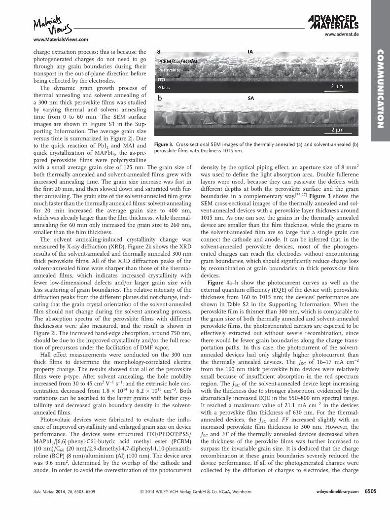
density by the optical piping effect, an aperture size of 8 mm 2 was used to defi ne the light absorption area. Double fullerene layers were used, because they can passivate the defects with different depths at both the perovskite surface and the grain boundaries in a complementary way. [ 26,27 ] Figure 3 shows the SEM cross-sectional images of the thermally annealed and sol-vent-annealed devices with a perovskite layer thickness around 1015 nm. As one can see, the grains in the thermally annealed device are smaller than the fi lm thickness, while the grains in the solvent-annealed fi lm are so large that a single grain can connect the cathode and anode. It can be inferred that, in the solvent-annealed perovskite devices, most of the photogen-erated charges can reach the electrodes without encountering grain boundaries, which should signifi cantly reduce charge loss by recombination at grain boundaries in thick perovskite fi lm devices.
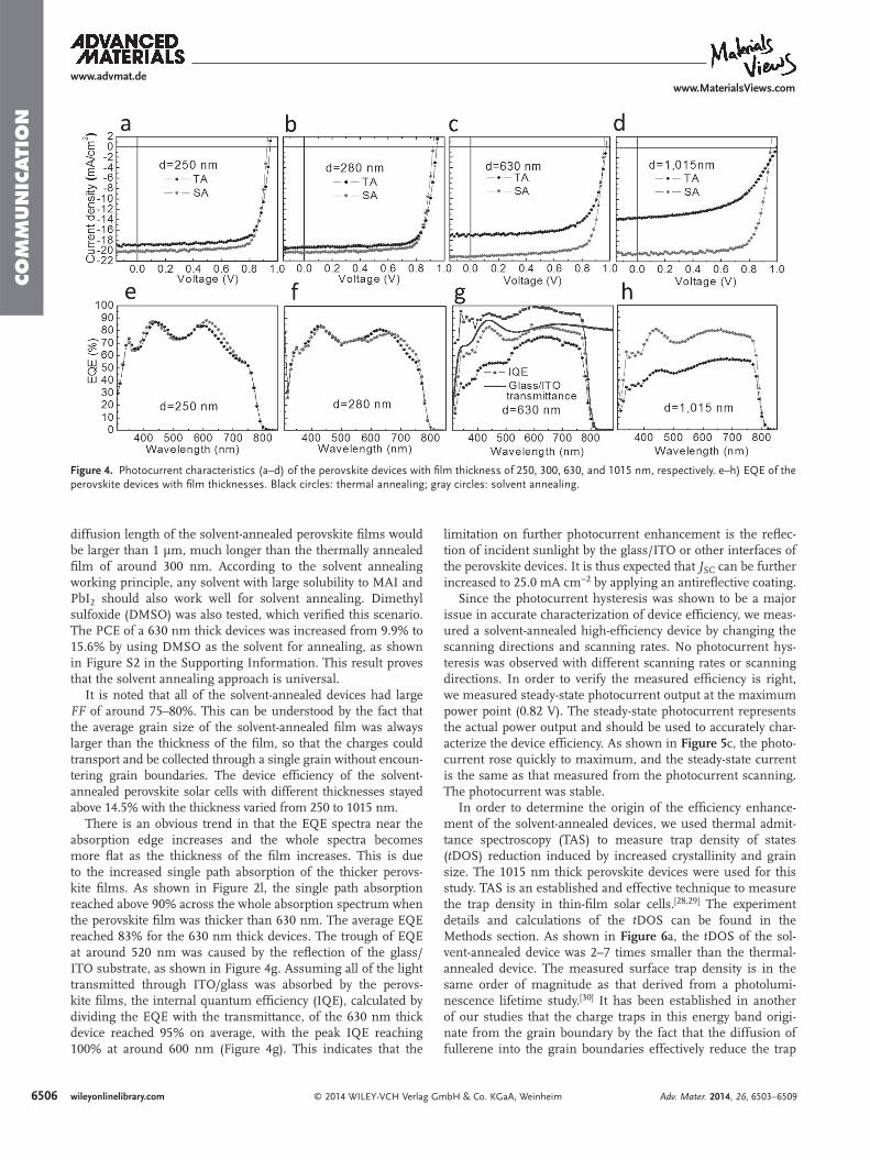
Figure 4 a–h show the photocurrent curves as well as the external quantum effi ciency (EQE) of the device with perovskite thickness from 160 to 1015 nm; the devices’ performance are shown in Table S2 in the Supporting Information. When the perovskite fi lm is thinner than 300 nm, which is comparable to the grain size of both thermally annealed and solvent-annealed perovskite fi lms, the photogenerated carriers are expected to be effectively extracted out without severe recombination, since there would be fewer grain boundaries along the charge trans-portation paths. In this case, the photocurrent of the solvent-annealed devices had only slightly higher photocurrent than the thermally annealed devices. The J SC of 16–17 mA cm −2 from the 160 nm thick perovskite fi lm devices were relatively small because of insuffi cient absorption in the red spectrum region. The J SC of the solvent-annealed device kept increasing with the thickness due to stronger absorption, evidenced by the dramatically increased EQE in the 550–800 nm spectral range. It reached a maximum value of 21.1 mA cm −2 in the devices with a perovskite fi lm thickness of 630 nm. For the thermal-annealed devices, the J SC and FF increased slightly with an increased perovskite fi lm thickness to 300 nm. However, the J SC and FF of the thermally annealed devices decreased when the thickness of the perovkite fi lms was further increased to surpass the invariable grain size. It is deduced that the charge recombination at these grain boundaries severely reduced the device performance. If all of the photogenerated charges were collected by the diffusion of charges to electrodes, the charge
Adv. Mater. 2014, 26, 6503–6509
www.advmat.dewww.MaterialsViews.com
Figure 3. Cross-sectional SEM images of the thermally annealed (a) and solvent-annealed (b) perovskite fi lms with thickness 1015 nm.
6506 wileyonlinelibrary.com © 2014 WILEY-VCH Verlag GmbH & Co. KGaA, Weinheim
CO
MM
UN
ICATI
ON
diffusion length of the solvent-annealed perovskite fi lms would be larger than 1 µm, much longer than the thermally annealed fi lm of around 300 nm. According to the solvent annealing working principle, any solvent with large solubility to MAI and PbI 2 should also work well for solvent annealing. Dimethyl sulf oxide (DMSO) was also tested, which verifi ed this scenario. The PCE of a 630 nm thick devices was increased from 9.9% to 15.6% by using DMSO as the solvent for annealing, as shown in Figure S2 in the Supporting Information. This result proves that the solvent annealing approach is universal.
It is noted that all of the solvent-annealed devices had large FF of around 75–80%. This can be understood by the fact that the average grain size of the solvent-annealed fi lm was always larger than the thickness of the fi lm, so that the charges could transport and be collected through a single grain without encoun-tering grain boundaries. The device effi ciency of the solvent-annealed perovskite solar cells with different thicknesses stayed above 14.5% with the thickness varied from 250 to 1015 nm.
There is an obvious trend in that the EQE spectra near the absorption edge increases and the whole spectra becomes more fl at as the thickness of the fi lm increases. This is due to the increased single path absorption of the thicker perovs-kite fi lms. As shown in Figure 2 l, the single path absorption reached above 90% across the whole absorption spectrum when the perovskite fi lm was thicker than 630 nm. The average EQE reached 83% for the 630 nm thick devices. The trough of EQE at around 520 nm was caused by the refl ection of the glass/ITO substrate, as shown in Figure 4 g. Assuming all of the light transmitted through ITO/glass was absorbed by the perovs-kite fi lms, the internal quantum effi ciency (IQE), calculated by dividing the EQE with the transmittance, of the 630 nm thick device reached 95% on average, with the peak IQE reaching 100% at around 600 nm (Figure 4 g). This indicates that the
limitation on further photocurrent enhancement is the refl ec-tion of incident sunlight by the glass/ITO or other interfaces of the perovskite devices. It is thus expected that J SC can be further increased to 25.0 mA cm −2 by applying an antirefl ective coating.
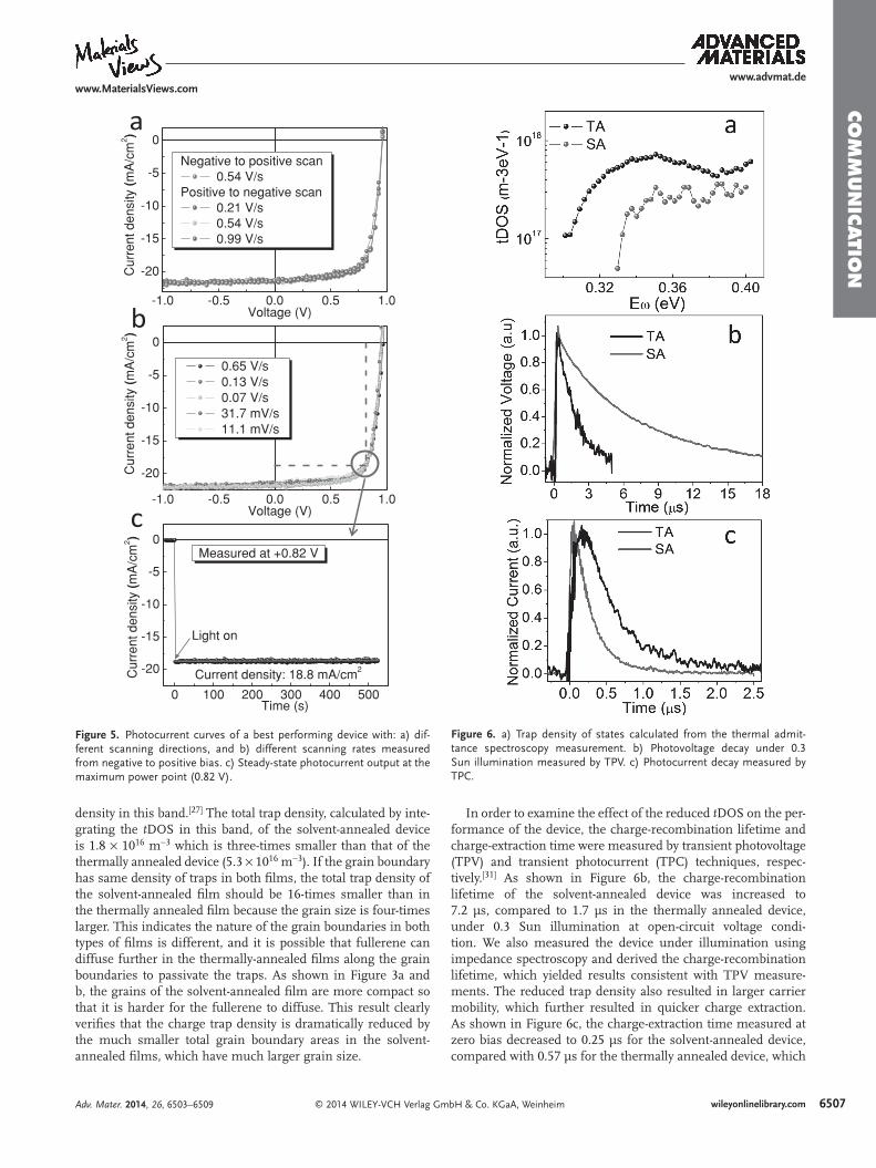
Since the photocurrent hysteresis was shown to be a major issue in accurate characterization of device effi ciency, we meas-ured a solvent-annealed high-effi ciency device by changing the scanning directions and scanning rates. No photocurrent hys-teresis was observed with different scanning rates or scanning directions. In order to verify the measured effi ciency is right, we measured steady-state photocurrent output at the maximum power point (0.82 V). The steady-state photocurrent represents the actual power output and should be used to accurately char-acterize the device effi ciency. As shown in Figure 5 c, the photo-current rose quickly to maximum, and the steady-state current is the same as that measured from the photocurrent scanning. The photocurrent was stable.
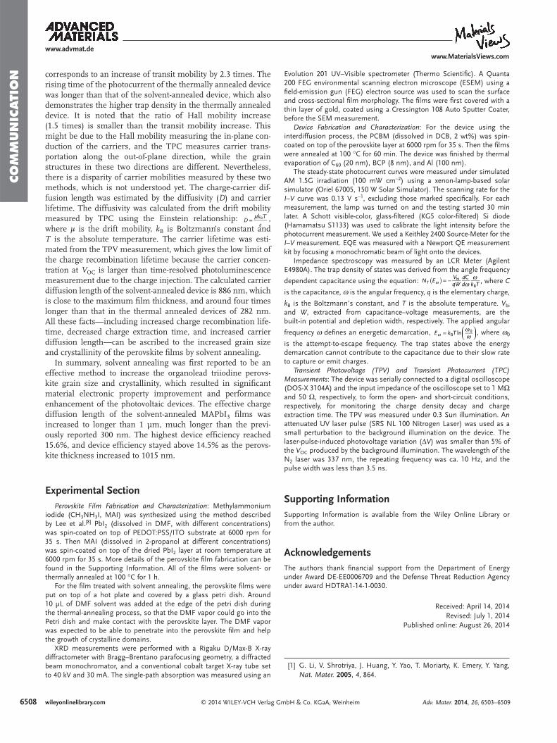
In order to determine the origin of the effi ciency enhance-ment of the solvent-annealed devices, we used thermal admit-tance spectroscopy (TAS) to measure trap density of states ( t DOS) reduction induced by increased crystallinity and grain size. The 1015 nm thick perovskite devices were used for this study. TAS is an established and effective technique to measure the trap density in thin-fi lm solar cells. [ 28,29 ] The experiment details and calculations of the t DOS can be found in the Methods section. As shown in Figure 6 a, the t DOS of the sol-vent-annealed device was 2–7 times smaller than the thermal-annealed device. The measured surface trap density is in the same order of magnitude as that derived from a photolumi-nescence lifetime study. [ 30 ] It has been established in another of our studies that the charge traps in this energy band origi-nate from the grain boundary by the fact that the diffusion of fullerene into the grain boundaries effectively reduce the trap
Adv. Mater. 2014, 26, 6503–6509
www.advmat.dewww.MaterialsViews.com
Figure 4. Photocurrent characteristics (a–d) of the perovskite devices with fi lm thickness of 250, 300, 630, and 1015 nm, respectively. e–h) EQE of the perovskite devices with fi lm thicknesses. Black circles: thermal annealing; gray circles: solvent annealing.
6507wileyonlinelibrary.com© 2014 WILEY-VCH Verlag GmbH & Co. KGaA, Weinheim
CO
MM
UN
ICATIO
N
density in this band. [ 27 ] The total trap density, calculated by inte-grating the t DOS in this band, of the solvent-annealed device is 1.8 × 10 16 m −3 which is three-times smaller than that of the thermally annealed device (5.3 × 10 16 m −3 ). If the grain boundary has same density of traps in both fi lms, the total trap density of the solvent-annealed fi lm should be 16-times smaller than in the thermally annealed fi lm because the grain size is four-times larger. This indicates the nature of the grain boundaries in both types of fi lms is different, and it is possible that fullerene can diffuse further in the thermally-annealed fi lms along the grain boundaries to passivate the traps. As shown in Figure 3 a and b, the grains of the solvent-annealed fi lm are more compact so that it is harder for the fullerene to diffuse. This result clearly verifi es that the charge trap density is dramatically reduced by the much smaller total grain boundary areas in the solvent-annealed fi lms, which have much larger grain size.
In order to examine the effect of the reduced t DOS on the per-formance of the device, the charge-recombination lifetime and charge-extraction time were measured by transient photovoltage (TPV) and transient photocurrent (TPC) techniques, respec-tively. [ 31 ] As shown in Figure 6 b, the charge-recombination lifetime of the solvent-annealed device was increased to 7.2 µs, compared to 1.7 µs in the thermally annealed device, under 0.3 Sun illumination at open-circuit voltage condi-tion. We also measured the device under illumination using impedance spectroscopy and derived the charge-recombination lifetime, which yielded results consistent with TPV measure-ments. The reduced trap density also resulted in larger carrier mobility, which further resulted in quicker charge extraction. As shown in Figure 6 c, the charge-extraction time measured at zero bias decreased to 0.25 µs for the solvent-annealed device, compared with 0.57 µs for the thermally annealed device, which
Adv. Mater. 2014, 26, 6503–6509
www.advmat.dewww.MaterialsViews.com
0 100 200 300 400 500
-20
-15
-10
-5
0
Light on
Measured at +0.82 V
Current density: 18.8 mA/cm2Cur
rent
den
sity
(m
A/c
m2 )
Time (s)
-1.0 -0.5 0.0 0.5 1.0
-20
-15
-10
-5
0
0.65 V/s 0.13 V/s 0.07 V/s 31.7 mV/s 11.1 mV/s
Cur
rent
den
sity
(m
A/c
m2 )
Voltage (V)
-1.0 -0.5 0.0 0.5 1.0
-20
-15
-10
-5
0
Negative to positive scan 0.54 V/s
Positive to negative scan 0.21 V/s 0.54 V/s 0.99 V/s
Cur
rent
den
sity
(m
A/c
m2 )
Voltage (V)
a
b
c
Figure 5. Photocurrent curves of a best performing device with: a) dif-ferent scanning directions, and b) different scanning rates measured from negative to positive bias. c) Steady-state photocurrent output at the maximum power point (0.82 V).
Figure 6. a) Trap density of states calculated from the thermal admit-tance spectroscopy measurement. b) Photovoltage decay under 0.3 Sun illumination measured by TPV. c) Photocurrent decay measured by TPC.
6508 wileyonlinelibrary.com © 2014 WILEY-VCH Verlag GmbH & Co. KGaA, Weinheim
CO
MM
UN
ICATI
ON corresponds to an increase of transit mobility by 2.3 times. The
rising time of the photocurrent of the thermally annealed device was longer than that of the solvent-annealed device, which also demonstrates the higher trap density in the thermally annealed device. It is noted that the ratio of Hall mobility increase (1.5 times) is smaller than the transit mobility increase. This might be due to the Hall mobility measuring the in-plane con-duction of the carriers, and the TPC measures carrier trans-portation along the out-of-plane direction, while the grain structures in these two directions are different. Nevertheless, there is a disparity of carrier mobilities measured by these two methods, which is not understood yet. The charge-carrier dif-fusion length was estimated by the diffusivity ( D ) and carrier lifetime. The diffusivity was calculated from the drift mobility measured by TPC using the Einstein relationship: μ
= BDk T
e,
where µ is the drift mobility, k B is Boltzmann’s constant and T is the absolute temperature. The carrier lifetime was esti-mated from the TPV measurement, which gives the low limit of the charge recombination lifetime because the carrier concen-tration at V OC is larger than time-resolved photoluminescence measurement due to the charge injection. The calculated carrier diffusion length of the solvent-annealed device is 886 nm, which is close to the maximum fi lm thickness, and around four times longer than that in the thermal annealed devices of 282 nm. All these facts—including increased charge recombination life-time, decreased charge extraction time, and increased carrier diffusion length—can be ascribed to the increased grain size and crystallinity of the perovskite fi lms by solvent annealing.
In summary, solvent annealing was fi rst reported to be an effective method to increase the organolead triiodine perovs-kite grain size and crystallinity, which resulted in signifi cant material electronic property improvement and performance enhancement of the photovoltaic devices. The effective charge diffusion length of the solvent-annealed MAPbI 3 fi lms was increased to longer than 1 µm, much longer than the previ-ously reported 300 nm. The highest device effi ciency reached 15.6%, and device effi ciency stayed above 14.5% as the perovs-kite thickness increased to 1015 nm.
Experimental Section Perovskite Film Fabrication and Characterization : Methylammonium
iodide (CH 3 NH 3 I, MAI) was synthesized using the method described by Lee et al. [ 8 ] PbI 2 (dissolved in DMF, with different concentrations) was spin-coated on top of PEDOT:PSS/ITO substrate at 6000 rpm for 35 s. Then MAI (dissolved in 2-propanol at different concentrations) was spin-coated on top of the dried PbI 2 layer at room temperature at 6000 rpm for 35 s. More details of the perovskite fi lm fabrication can be found in the Supporting Information. All of the fi lms were solvent- or thermally annealed at 100 °C for 1 h.
For the fi lm treated with solvent annealing, the perovskite fi lms were put on top of a hot plate and covered by a glass petri dish. Around 10 µL of DMF solvent was added at the edge of the petri dish during the thermal-annealing process, so that the DMF vapor could go into the Petri dish and make contact with the perovskite layer. The DMF vapor was expected to be able to penetrate into the perovskite fi lm and help the growth of crystalline domains.
XRD measurements were performed with a Rigaku D/Max-B X-ray diffractometer with Bragg–Brentano parafocusing geometry, a diffracted beam monochromator, and a conventional cobalt target X-ray tube set to 40 kV and 30 mA. The single-path absorption was measured using an
Evolution 201 UV–Visible spectrometer (Thermo Scientifi c). A Quanta 200 FEG environmental scanning electron microscope (ESEM) using a fi eld-emission gun (FEG) electron source was used to scan the surface and cross-sectional fi lm morphology. The fi lms were fi rst covered with a thin layer of gold, coated using a Cressington 108 Auto Sputter Coater, before the SEM measurement.
Device Fabrication and Characterization : For the device using the interdiffusion process, the PCBM (dissolved in DCB, 2 wt%) was spin-coated on top of the perovskite layer at 6000 rpm for 35 s. Then the fi lms were annealed at 100 °C for 60 min. The device was fi nished by thermal evaporation of C 60 (20 nm), BCP (8 nm), and Al (100 nm).
The steady-state photocurrent curves were measured under simulated AM 1.5G irradiation (100 mW cm −2 ) using a xenon-lamp-based solar simulator (Oriel 67005, 150 W Solar Simulator). The scanning rate for the I – V curve was 0.13 V s −1 , excluding those marked specifi cally. For each measurement, the lamp was turned on and the testing started 30 min later. A Schott visible-color, glass-fi ltered (KG5 color-fi ltered) Si diode (Hamamatsu S1133) was used to calibrate the light intensity before the photocurrent measurement. We used a Keithley 2400 Source-Meter for the I – V measurement. EQE was measured with a Newport QE measurement kit by focusing a monochromatic beam of light onto the devices.
Impedance spectroscopy was measured by an LCR Meter (Agilent E4980A). The trap density of states was derived from the angle frequency
dependent capacitance using the equation: Tbi
BN E
VqW
dCd k Tω
ω( ) = −ω , where C
is the capacitance, ω is the angular frequency, q is the elementary charge,
k B is the Boltzmann’s constant, and T is the absolute temperature. V bi and W , extracted from capacitance–voltage measurements, are the built-in potential and depletion width, respectively. The applied angular
frequency ω defi nes an energetic demarcation, lnB0E k T
ωω= ⎛
⎝⎜⎞⎠⎟ω , where ω 0
is the attempt-to-escape frequency. The trap states above the energy demarcation cannot contribute to the capacitance due to their slow rate to capture or emit charges.
Transient Photovoltage (TPV) and Transient Photocurrent (TPC) Measurements : The device was serially connected to a digital oscilloscope (DOS-X 3104A) and the input impedance of the oscilloscope set to 1 MΩ and 50 Ω, respectively, to form the open- and short-circuit conditions, respectively, for monitoring the charge density decay and charge extraction time. The TPV was measured under 0.3 Sun illumination. An attenuated UV laser pulse (SRS NL 100 Nitrogen Laser) was used as a small perturbation to the background illumination on the device. The laser-pulse-induced photovoltage variation (Δ V ) was smaller than 5% of the V OC produced by the background illumination. The wavelength of the N 2 laser was 337 nm, the repeating frequency was ca. 10 Hz, and the pulse width was less than 3.5 ns.
Supporting Information Supporting Information is available from the Wiley Online Library or from the author.
Acknowledgements The authors thank fi nancial support from the Department of Energy under Award DE-EE0006709 and the Defense Threat Reduction Agency under award HDTRA1-14-1-0030.
Received: April 14, 2014 Revised: July 1, 2014
Published online: August 26, 2014
[1] G. Li , V. Shrotriya , J. Huang , Y. Yao , T. Moriarty , K. Emery , Y. Yang , Nat. Mater. 2005 , 4 , 864 .
Adv. Mater. 2014, 26, 6503–6509
www.advmat.dewww.MaterialsViews.com
6509wileyonlinelibrary.com© 2014 WILEY-VCH Verlag GmbH & Co. KGaA, Weinheim
CO
MM
UN
ICATIO
N
[2] X. Liu , H. Wang , T. Yang , W. Zhang , X. Gong , ACS Appl. Mater. Inter-faces 2012 , 4 , 3701 .
[3] G. Li , Y. Yao , H. Yang , V. Shrotriya , G. Yang , Y. Yang , Adv. Funct. Mater. 2007 , 17 , 1636 .
[4] Q. Chen , H. Zhou , Z. Hong , S. Luo , H.-S. Duan , H.-H. Wang , Y. Liu , G. Li , Y. Yang , J. Am. Chem. Soc. 2013 , 136 , 622 .
[5] J. Burschka , N. Pellet , S.-J. Moon , R. Humphry-Baker , P. Gao , M. K. Nazeeruddin , M. Grätzel , Nature 2013 , 499 , 316 .
[6] M. Liu , M. B. Johnston , H. J. Snaith , Nature 2013 , 501 , 395 . [7] A. Kojima , K. Teshima , Y. Shirai , T. Miyasaka , J. Am. Chem. Soc.
2009 , 131 , 6050 . [8] M. M. Lee , J. Teuscher , T. Miyasaka , T. N. Murakami , H. J. Snaith ,
Science 2012 , 338 , 643 . [9] A. Abrusci , S. D. Stranks , P. Docampo , H.-L. Yip , A. K. Y. Jen ,
H. J. Snaith , Nano Lett. 2013 , 13 , 3124 . [10] J. M. Ball , M. M. Lee , A. Hey , H. J. Snaith , Energy Environ. Sci. 2013 ,
6 , 1739 . [11] G. Hodes , Science 2013 , 342 , 317 . [12] J. Y. Jeng , Y. F. Chiang , M. H. Lee , S. R. Peng , T. F. Guo , P. Chen ,
T. C. Wen , Adv. Mater. 2013 , 25 , 3727 . [13] H.-S. Kim , I. Mora-Sero , V. Gonzalez-Pedro , F. Fabregat-Santiago ,
E. J. Juarez-Perez , N.-G. Park , J. Bisquert , Nat. Commun. 2013 , 4 , 2242 . [14] H. J. Snaith , J. Phys.Chem. Lett. 2013 , 4 , 3623 . [15] S. D. Stranks , G. E. Eperon , G. Grancini , C. Menelaou , M. J. Alcocer ,
T. Leijtens , L. M. Herz , A. Petrozza , H. J. Snaith , Science 2013 , 342 , 341 . [16] W. Zhang , M. Saliba , S. D. Stranks , Y. Sun , X. Shi , U. Wiesner ,
H. J. Snaith , Nano Lett. 2013 , 13 , 4505 . [17] G. Xing , N. Mathews , S. Sun , S. S. Lim , Y. M. Lam , M. Grätzel ,
S. Mhaisalkar , T. C. Sum , Science 2013 , 342 , 344 .
[18] J. H. Heo , S. H. Im , J. H. Noh , T. N. Mandal , C.-S. Lim , J. A. Chang , Y. H. Lee , H.-j. Kim , A. Sarkar , M. K. Nazeeruddin , Nat. Photonics 2013 , 7 , 486 .
[19] P. Docampo , J. M. Ball , M. Darwich , G. E. Eperon , H. J. Snaith , Nat. Commun. 2013 , 4 , 2761 .
[20] E. Edri , S. Kirmayer , A. Henning , S. Mukhopadhyay , K. Gartsman , Y. Rosenwaks , G. Hodes , D. Cahen , Nano Lett. 2014 , 14 , 1000 .
[21] C. E. Small , S. W. Tsang , S. Chen , S. Baek , C. M. Amb , J. Subbiah , J. R. Reynolds , F. So , Adv. Energ. Mater. 2013 , 3 , 909 .
[22] A. Dualeh , N. Tétreault , T. Moehl , P. Gao , M. K. Nazeeruddin , M. Grätzel , Adv. Funct. Mater. 2014 , 24 , 3250 .
[23] C. Bi , Y. Shao , Y. Yuan , Z. Xiao , C. Wang , Y. Gao , J. Huang , unpublished .
[24] Z. Xiao , C. Bi , Y. Shao , Q. Dong , Q. Wang , C. Wang , Y. Gao , J. Huang , Energy Environ. Sci. 2014 , 7 , 2619 .
[25] C. Thompson , Ann. Rev. Mater. Sci. 2000 , 30 , 159 . [26] Q. Wang , Y. Shao , Q. Dong , Z. Xiao , Y. Yuan , J. Huang , Energy
Environ. Sci. 2014 , 7 , 2359 . [27] Y. Shao , Z. Xiao , Q. Wang , Y. Gao , J. Huang , unpublished . [28] T. Walter , R. Herberholz , C. Müller , H. Schock , J. Appl. Phys. 1996 ,
80 , 4411 . [29] Advanced Characterization Techniques for Thin Film Solar Cells , (Eds:
U. Rau , D. Abou-Ras , T. Kirchartz ), Wiley , Weinheim, Germany, 2011 .
[30] G. Xing , N. Mathews , S. S. Lim , N. Yantara , X. Liu , D. Sabba , M. Grätzel , S. Mhaisalkar , T. C. Sum , Nat. Mater. 2014 , 13 , 476 .
[31] C. Shuttle , B. ORegan , A. Ballantyne , J. Nelson , D. Bradley , J. De Mello , J. Durrant , Appl. Phys. Lett. 2008 , 92 , 093311 .
Adv. Mater. 2014, 26, 6503–6509
www.advmat.dewww.MaterialsViews.com