skp engineering college · s.k.p. engineering college, tiruvannamalai iv sem
TRANSCRIPT
S.K.P. Engineering College, Tiruvannamalai IV SEM
Electronics and Communication Engineering Department 1 Electronics Circuits II
SKP Engineering College
Tiruvannamalai – 606611
A Course Material
on Electronics Circuits-II
By
M.Jerin Jose
Associate Professor
Electronics and Communication Engineering Department

S.K.P. Engineering College, Tiruvannamalai IV SEM
Electronics and Communication Engineering Department 2 Electronics Circuits II
Quality Certificate
This is to Certify that the Electronic Study Material
Subject Code: EC6401
Subject Name: Electronics Circuits II
Year/Sem: II/IV
Being prepared by me and it meets the knowledge requirement of the University curriculum.
Signature of the Author
Name: M.Jerin Jose
Designation: Assistant Professor
This is to certify that the course material being prepared by Mr. M.Jerin Jose is of the adequate quality. He has referred more than five books and one among them is from abroad author.
Signature of HD Signature of the Principal
Name: Mr.R.Saravanakumar Name: Dr.V.Subramania Bharathi
Seal: Seal:
S.K.P. Engineering College, Tiruvannamalai IV SEM
Electronics and Communication Engineering Department 3 Electronics Circuits II
EC6401 Electronic circuits II L T P C 3 0 0 3
Objective:
• To understand the advantages and method of analysis of feedback amplifiers. • To understand the analysis and design of LC and RC oscillators • To understand the analysis and design of tuned amplifier. • To understand the analysis and design of multivibrators • To understand the analysis and design of blocking oscillators and time base
generator
UNIT I FEEDBACK AMPLIFIERS 9
General Feedback Structure – Properties of negative feedback – Basic Feedback Topologies – Feedback amplifiers – Series – Shunt, Series – Series, Shunt – Shunt and Shunt – Series Feedback – Determining the Loop Gain – Stability Problem – Nyquist Plot – Effect of feedback on amplifier poles – Frequency Compensation.
UNIT II OSCILLATORS 9
Classification, Barkhausen Criterion - Mechanism for start of oscillation and stabilization of amplitude, General form of an Oscillator, Analysis of LC oscillators - Hartley, Colpitts,Clapp, Franklin, Armstrong, Tuned collector oscillators, RC oscillators - phase shift –Wienbridge - Twin-T Oscillators, Frequency range of RC and LC Oscillators, Quartz Crystal Construction, Electrical equivalent circuit of Crystal, Miller and Pierce Crystal oscillators, frequency stability of oscillators.
UNIT III TUNED AMPLIFIERS 9
Coil losses, unloaded and loaded Q of tank circuits, small signal tuned amplifiers - Analysis of capacitor coupled single tuned amplifier – double tuned amplifier - effect of cascading single tuned and double tuned amplifiers on bandwidth – Stagger tuned amplifiers – large signal tuned amplifiers – Class C tuned amplifier – Efficiency and applications of Class C tuned amplifier - Stability of tuned amplifiers – Neutralization - Hazeltine neutralization method.
UNIT IV WAVE SHAPING AND MULTIVIBRATOR CIRCUITS 9
RC & RL Integrator and Differentiator circuits – Storage, Delay and Calculation of Transistor Switching Times – Speed-up Capaitor - Diode clippers, Diode comparator - Clampers. Collector coupled and Emitter coupled Astable multivibrator – Monostable multivibrator - Bistable multivibrators - Triggering methods for Bistable multivibrators - Schmitt trigger circuit.
UNIT V BLOCKING OSCILLATORS AND TIMEBASE GENERATORS 9
UJT saw tooth waveform generator, Pulse transformers – equivalent circuit – response - applications, Blocking Oscillator – Free running blocking oscillator - Astable Blocking Oscillators with base timing – Push-pull Astable blocking oscillator with emitter timing, Frequency control using core saturation, Triggered blocking oscillator – Monostable

S.K.P. Engineering College, Tiruvannamalai IV SEM
Electronics and Communication Engineering Department 4 Electronics Circuits II
blocking oscillator with base timing – Monostable blocking oscillator with emitter timing, Time base circuits - Voltage-Time base circuit, Current-Time base circuit-– Linearization through adjustment of driving waveform.
OUTCOMES:
Upon Completion of the course, the students will be able to:
• Design circuits with transistor biasing. • Design simple amplifier circuits. • Analyze the small signal equivalent circuits of transistors. • Design and analyze small signal amplifiers. • Design and analyze large signal amplifiers.
TEXT BOOK:
Donald .A. Neamen, Electronic Circuit Analysis and Desig 2nd Edition,Tata Mc Graw Hill, 2009.
REFERENCES:
1. Adel .S. Sedra, Kenneth C. Smith, “Micro Electronic Circuits”, 6th Edition, Oxford UniversityPress, 2010. 2. David A., “Bell Electronic Devices and Circuits”, Oxford Higher Education Press, 5th Edition,2010 3. Behzad Razavi, “Design of Analog CMOS Integrated Circuits”, Tata Mc Graw Hill, 2007. 4. Paul Gray, Hurst, Lewis, Meyer “Analysis and Design of Analog Integrated Circuits”,4th Edition ,John Willey & Sons 2005 5. Millman.J. and Halkias C.C, “Integrated Electronics”, Mc Graw Hill, 2001. 6. D.Schilling and C.Belove, “Electronic Circuits”, 3rd Edition, Mc Graw Hill, 1989. 7. Robert L. Boylestad and Louis Nasheresky, “Electronic Devices and Circuit Theory”, 10th Edition, Pearson Education / PHI, 2008

S.K.P. Engineering College, Tiruvannamalai IV SEM
Electronics and Communication Engineering Department 5 Electronics Circuits II
CONTENTS
S.No Particulars Page
1 Unit – I 5
2 Unit – II 23
3 Unit – III 56
4 Unit – IV 63
5 Unit – V 82
S.K.P. Engineering College, Tiruvannamalai IV SEM
Electronics and Communication Engineering Department 6 Electronics Circuits II
Unit – I
Feed Back Amplifiers
Part-A
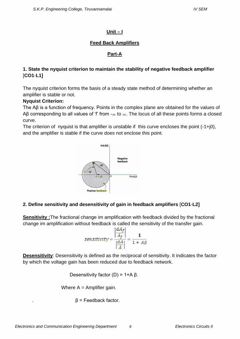
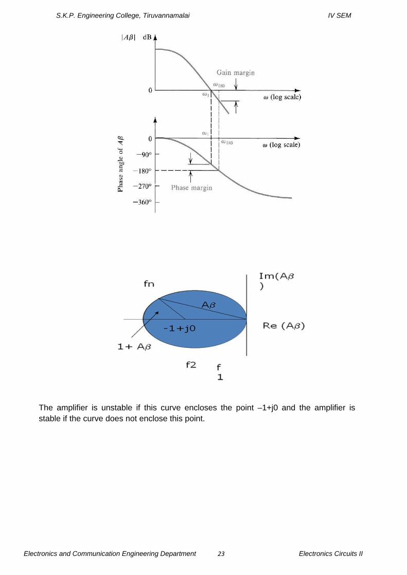
1. State the nyquist criterion to maintain the stability of negative feedback amplifier [CO1-L1] The nyquist criterion forms the basis of a steady state method of determining whether an amplifier is stable or not. Nyquist Criterion: The Aβ is a function of frequency. Points in the complex plane are obtained for the values of Aβ corresponding to all values of ‘f’ from - to . The locus of all these points forms a closed curve. The criterion of nyquist is that amplifier is unstable if this curve encloses the point (-1+j0), and the amplifier is stable if the curve does not enclose this point.
2. Define sensitivity and desensitivity of gain in feedback amplifiers [CO1-L2] Sensitivity :The fractional change im amplification with feedback divided by the fractional change im amplification without feedback is called the sensitivity of the transfer gain. Desensitivity: Desensitivity is defined as the reciprocal of sensitivity. It indicates the factor by which the voltage gain has been reduced due to feedback network.
Desensitivity factor (D) = 1+A β.
Where A = Amplifier gain.
. β = Feedback factor.
S.K.P. Engineering College, Tiruvannamalai IV SEM
Electronics and Communication Engineering Department 7 Electronics Circuits II
3. What is the effect on input and output impendence of an amplifier if it employs voltage series negative feedback? [CO1-L2] When voltage series feedback is employed in an amplifier, its input resistance increases and output resistance decreases
4. Define ‘feedback factor’ of a feedback amplifier.[CO1-L3]
It is the ratio between the feedback voltages to the output voltage of the amplifier.
β = Vf/ Vo
Where β is a feedback factor (or) feedback ratio. Vf is the feedback voltage. Vo is the output voltage.
4. What is the impact of negativefeedback on noise in circuits? [CO1-L1] When negative feedback is employed in an amlifier ,the noise is reduced. Let N= noise without feedback
Nf = noise with feedback From above equation it is clear that when the feedback is applied the noise is reduced by a factor (1+Aβ) 6. What is the effect on input and output impendence of an amplifier if it employs
current shunt negative feedback? [CO1-L2] When current shunt feedback is employed in an amplifier, its input resistance decreases and output resistance increases 7. What is return ratio of feedback amplifier? [CO1-L1]
A path of a signal from input terminals through basic amplifier, through the feedback network and back to the input terminals forms a loop. The gain of this loop is the product of –Aβ. This gain is known as loop gain or return ratio. Here the minus sign indicates the negative feedback 8. Justify that negative feedback amplifier increases bandwidth. [CO1-L2] When negative feedback is employed in an amlifier ,the bandwidth is increased. Let BW= bandwidth without feedback
BWf = bandwidth with feedback
The bandwidth with feedback is given by the following relation, From above equation it is clear that when the feedback is applied the bandwidth is increased is by a factor (1+Aβ)
S.K.P. Engineering College, Tiruvannamalai IV SEM
Electronics and Communication Engineering Department 8 Electronics Circuits II
9. Distinguish between series and shunt feedback amplifiers Series feedback [CO1-L1]
Series feedback: (i)In series feedback amplifier the feedback signal is connected in series with the input signal. (ii). It increases the input resistance. Shunt feedback: (i). In shunt feedback amplifier the feedback signal is connected in shunt with the input signal. (ii). It decreases the input resistance.
10. What is current-series feedback amplifier [CO1-L1] In a current series feedback amplifier the sampled signal is a current and the feedback signal (Which is fed in series)is a voltage.
Gm =Io / Vi Where Gm = Amplifier gain.
Io = Output current. Vi = Input voltage.
11. List the four basic feedback topologies. [CO1-L1] Current series feedback. Current shunt feedback. Voltage series feedback Voltage shunt feedback 12. List the characteristics of an amplifier which are modified by
Negative feedback [CO1-L1] It reduces the gain of an amplifier It increases the stability of an amplifier. It increases the bandwidth It decreases noise and distortion
13. What is Feedback Amplifier? & draw the diagram. [CO1-L1] An amplifier with feedback network is known as feedback amplifier. With the help of feedback network, ‘a portion of the output signal is fed back to the input & combined with the input signal to produce the desired outputs’ 14. Mention the three networks that are connected around the basic Amplifier to
implement the feedback concept.[NOV/DEC 2012] [CO1-L2]
The three networks that are connected around the basic amplifier to implement the feedback concept are
o Mixing Network o Sampling Network o Feedback Network
S.K.P. Engineering College, Tiruvannamalai IV SEM
Electronics and Communication Engineering Department 9 Electronics Circuits II
15. What happens to the input resistance based on the type of feedback in an amplifier?[MAY/JUNE 2009] [CO1-L2]
• If the feedback signal is added to the input in series with the applied voltage, it increases the input resistance.
• If the feedback signal is added to the input in shunt with the applied voltage, it decreases the input resistance.
16. What are the steps to be carried out for complete analysis of a feedback Amplifier? [MAY/JUNE 2009] [CO1-L1] Step 1: Identify the topology Step 2,3: Find input and output circuit Step 4: Replace transistor by its h-parameter equivalent circuit Step 5: Find open loop voltage gain Step 6: Indicate V0 and Vf and calculate β Step 7: Calculate D, Avf, Rif, Rof and
Part-B
1. Derive the expressions for gain with positive and negative feedback?
[CO1-H1]
The process of injecting a fraction of output energy of some device back to the input is known as feedback. The principle of feedback is probably as old as the invention of first machine but it is only some 50 years ago that feedback has come into use in connection with electronic circuits. It has been found very useful in reducing noise in amplifiers and making amplifier operation stable. Depending upon whether the feedback energy aids or opposes the input signal, there are two basic types of feedback in amplifiers viz positive feedback and negative feedback.
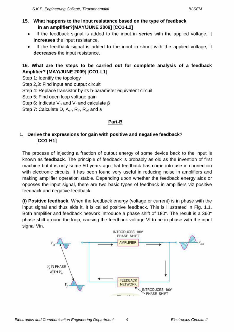
(i) Positive feedback. When the feedback energy (voltage or current) is in phase with the input signal and thus aids it, it is called positive feedback. This is illustrated in Fig. 1.1. Both amplifier and feedback network introduce a phase shift of 180°. The result is a 360° phase shift around the loop, causing the feedback voltage Vf to be in phase with the input signal Vin.

S.K.P. Engineering College, Tiruvannamalai IV SEM
Electronics and Communication Engineering Department 10 Electronics Circuits II
The positive feedback increases the gain of the amplifier. However, it has the disadvantages of increased distortion and instability. Therefore, positive feedback is seldom employed in amplifiers. One important use of positive feedback is in oscillators.
As we shall see in the next chapter, if positive feedback is sufficiently large, it leads to oscillations. As a matter of fact, an oscillator is a device that converts d.c. power into a.c. power of any desired frequency.
(ii) Negative feedback. When the feedback energy (voltage or current) is out of phase with the input signal and thus opposes it, it is called negative feedback. This is illustrated in Fig. 1.2. As you can see, the amplifier introduces a phase shift of 180° into the circuit while the feedback network is so designed that it introduces no phase shift (i.e., 0° phase shift). The result is that the feedback voltage Vf is 180° out of phase with the input signal Vin.
Negative feedback reduces the gain of the amplifier. However, the advantages of negative feedback are: reduction in distortion, stability in gain, increased bandwidth and improved input and output impedances. It is due to these advantages that negative feedback is frequently employed in amplifiers.
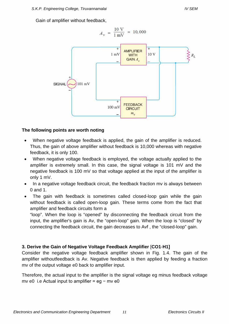
2. Write the Principles of Negative Voltage Feedback In Amplifiers. [CO1-H2] A feedback amplifier has two parts viz an amplifier and a feedback circuit. The feedback circuit usually consists of resistors and returns a fraction of output energy back to the input. Fig. 1.3 *shows the principles of negative voltage feedback in an amplifier. Typical values have been assumed to make the treatment more illustrative. The output of the amplifier is 10 V. The fraction mv of this output i.e. 100 mV is fedback to the input where it is applied in series with the input signal of 101 mV. As the feedback is negative, therefore, only 1 mV appears at the input terminals of the amplifier. Referring to Fig. 1.3, we have,
S.K.P. Engineering College, Tiruvannamalai IV SEM
Electronics and Communication Engineering Department 11 Electronics Circuits II
Gain of amplifier without feedback,
The following points are worth noting
• When negative voltage feedback is applied, the gain of the amplifier is reduced. Thus, the gain of above amplifier without feedback is 10,000 whereas with negative feedback, it is only 100.
• When negative voltage feedback is employed, the voltage actually applied to the amplifier is extremely small. In this case, the signal voltage is 101 mV and the negative feedback is 100 mV so that voltage applied at the input of the amplifier is only 1 mV.
• In a negative voltage feedback circuit, the feedback fraction mv is always between 0 and 1.
• The gain with feedback is sometimes called closed-loop gain while the gain without feedback is called open-loop gain. These terms come from the fact that amplifier and feedback circuits form a
“loop”. When the loop is “opened” by disconnecting the feedback circuit from the input, the amplifier's gain is Av, the “open-loop” gain. When the loop is “closed” by connecting the feedback circuit, the gain decreases to Avf , the “closed-loop” gain.
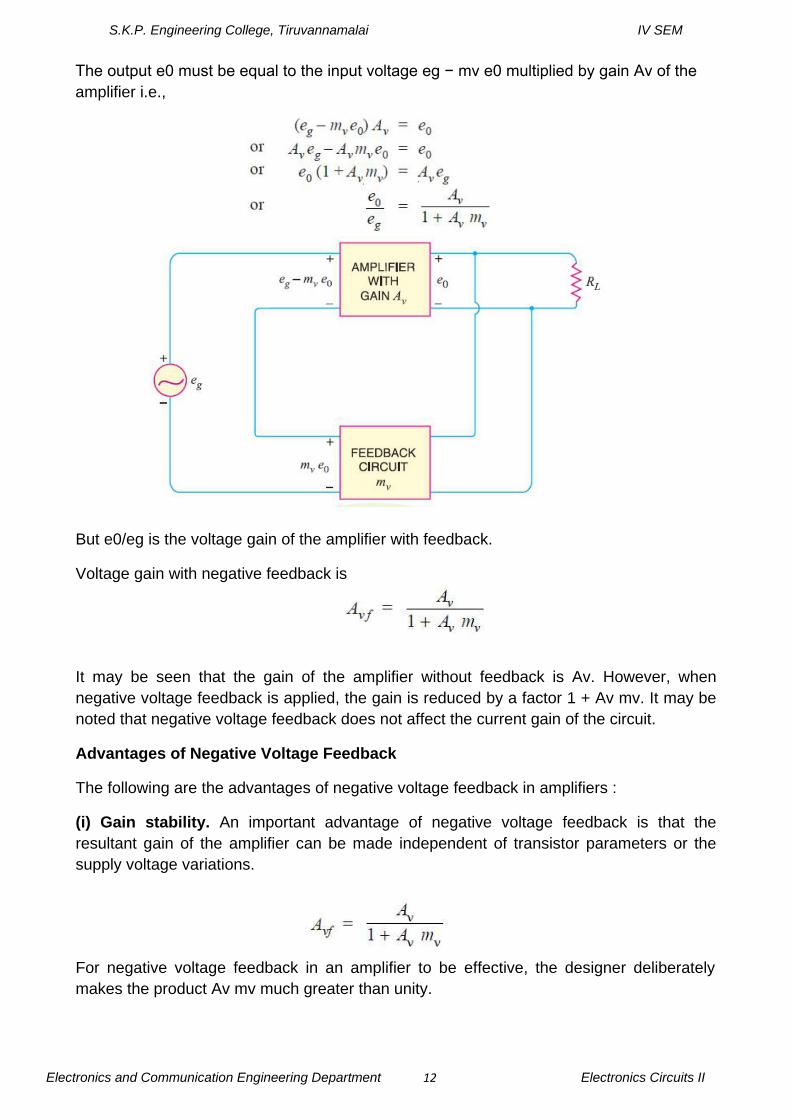
3. Derive the Gain of Negative Voltage Feedback Amplifier [CO1-H1] Consider the negative voltage feedback amplifier shown in Fig. 1.4. The gain of the amplifier withoutfeedback is Av. Negative feedback is then applied by feeding a fraction mv of the output voltage e0 back to amplifier input.
Therefore, the actual input to the amplifier is the signal voltage eg minus feedback voltage mv e0 i.e Actual input to amplifier = eg − mv e0
S.K.P. Engineering College, Tiruvannamalai IV SEM
Electronics and Communication Engineering Department 12 Electronics Circuits II
The output e0 must be equal to the input voltage eg − mv e0 multiplied by gain Av of the amplifier i.e.,
But e0/eg is the voltage gain of the amplifier with feedback.
Voltage gain with negative feedback is
It may be seen that the gain of the amplifier without feedback is Av. However, when negative voltage feedback is applied, the gain is reduced by a factor 1 + Av mv. It may be noted that negative voltage feedback does not affect the current gain of the circuit.
Advantages of Negative Voltage Feedback
The following are the advantages of negative voltage feedback in amplifiers :
(i) Gain stability. An important advantage of negative voltage feedback is that the resultant gain of the amplifier can be made independent of transistor parameters or the supply voltage variations.
For negative voltage feedback in an amplifier to be effective, the designer deliberately makes the product Av mv much greater than unity.
S.K.P. Engineering College, Tiruvannamalai IV SEM
Electronics and Communication Engineering Department 13 Electronics Circuits II
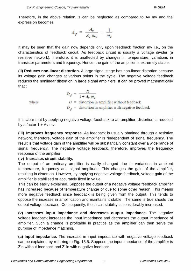
Therefore, in the above relation, 1 can be neglected as compared to Av mv and the expression becomes
It may be seen that the gain now depends only upon feedback fraction mv i.e., on the characteristics of feedback circuit. As feedback circuit is usually a voltage divider (a resistive network), therefore, it is unaffected by changes in temperature, variations in transistor parameters and frequency. Hence, the gain of the amplifier is extremely stable.
(ii) Reduces non-linear distortion. A large signal stage has non-linear distortion because its voltage gain changes at various points in the cycle. The negative voltage feedback reduces the nonlinear distortion in large signal amplifiers. It can be proved mathematically that :
It is clear that by applying negative voltage feedback to an amplifier, distortion is reduced by a factor 1 + Av mv.
(iii) Improves frequency response. As feedback is usually obtained through a resistive network, therefore, voltage gain of the amplifier is *independent of signal frequency. The result is that voltage gain of the amplifier will be substantially constant over a wide range of signal frequency. The negative voltage feedback, therefore, improves the frequency response of the amplifier. (iv) Increases circuit stability. The output of an ordinary amplifier is easily changed due to variations in ambient temperature, frequency and signal amplitude. This changes the gain of the amplifier, resulting in distortion. However, by applying negative voltage feedback, voltage gain of the amplifier is stabilised or accurately fixed in value. This can be easily explained. Suppose the output of a negative voltage feedback amplifier has increased because of temperature change or due to some other reason. This means more negative feedback since feedback is being given from the output. This tends to oppose the increase in amplification and maintains it stable. The same is true should the output voltage decrease. Consequently, the circuit stability is considerably increased.
(v) Increases input impedance and decreases output impedance. The negative voltage feedback increases the input impedance and decreases the output impedance of amplifier. Such a change is profitable in practice as the amplifier can then serve the purpose of impedance matching.
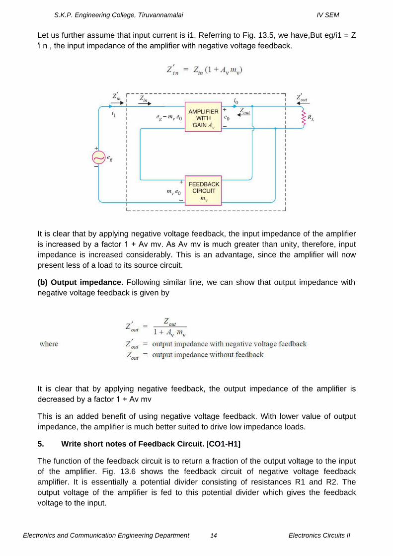
(a) Input impedance. The increase in input impedance with negative voltage feedback can be explained by referring to Fig. 13.5. Suppose the input impedance of the amplifier is Zin without feedback and Z ′in with negative feedback.
S.K.P. Engineering College, Tiruvannamalai IV SEM
Electronics and Communication Engineering Department 14 Electronics Circuits II
Let us further assume that input current is i1. Referring to Fig. 13.5, we have,But eg/i1 = Z ′i n , the input impedance of the amplifier with negative voltage feedback.
It is clear that by applying negative voltage feedback, the input impedance of the amplifier is increased by a factor 1 + Aν mv. As Aν mv is much greater than unity, therefore, input impedance is increased considerably. This is an advantage, since the amplifier will now present less of a load to its source circuit.
(b) Output impedance. Following similar line, we can show that output impedance with negative voltage feedback is given by
It is clear that by applying negative feedback, the output impedance of the amplifier is decreased by a factor 1 + Aν mν
This is an added benefit of using negative voltage feedback. With lower value of output impedance, the amplifier is much better suited to drive low impedance loads.
5. Write short notes of Feedback Circuit. [CO1-H1]
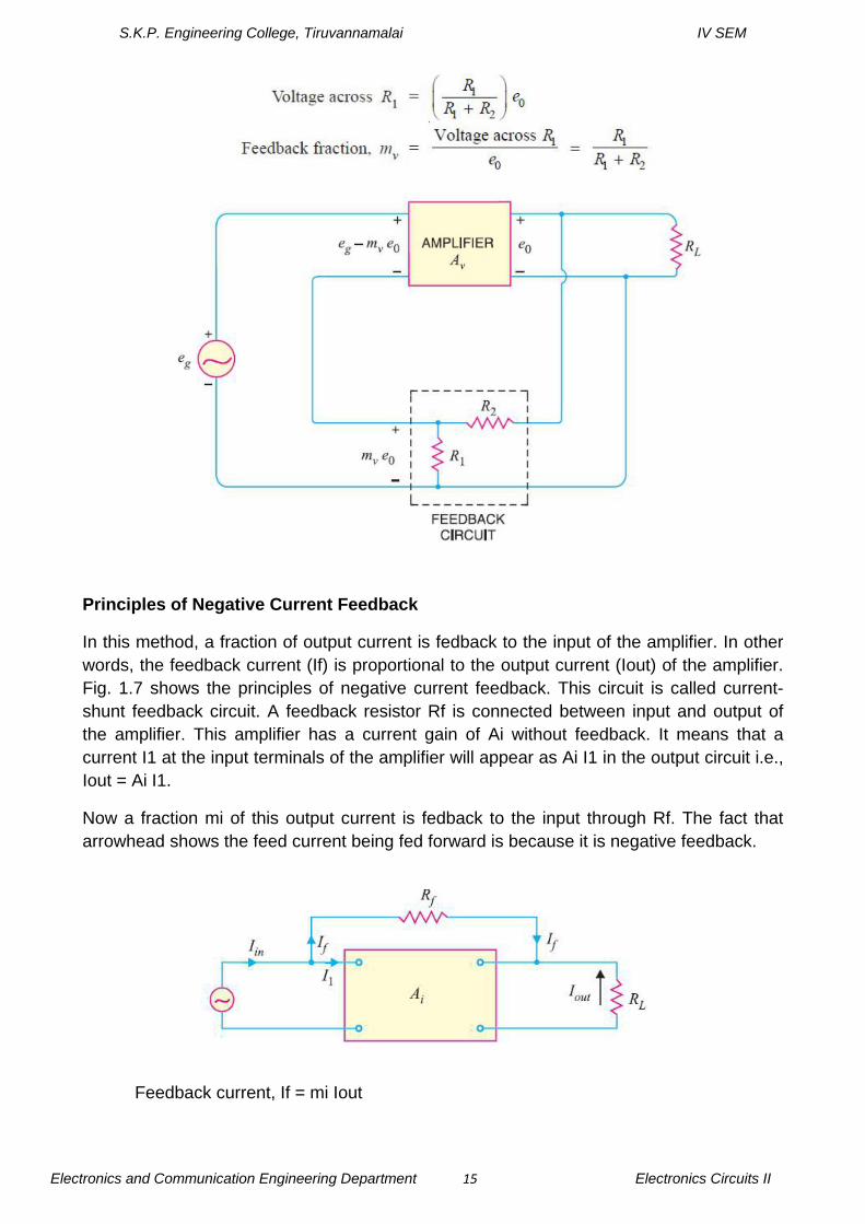
The function of the feedback circuit is to return a fraction of the output voltage to the input of the amplifier. Fig. 13.6 shows the feedback circuit of negative voltage feedback amplifier. It is essentially a potential divider consisting of resistances R1 and R2. The output voltage of the amplifier is fed to this potential divider which gives the feedback voltage to the input.
S.K.P. Engineering College, Tiruvannamalai IV SEM
Electronics and Communication Engineering Department 15 Electronics Circuits II
Principles of Negative Current Feedback
In this method, a fraction of output current is fedback to the input of the amplifier. In other words, the feedback current (If) is proportional to the output current (Iout) of the amplifier. Fig. 1.7 shows the principles of negative current feedback. This circuit is called current-shunt feedback circuit. A feedback resistor Rf is connected between input and output of the amplifier. This amplifier has a current gain of Ai without feedback. It means that a current I1 at the input terminals of the amplifier will appear as Ai I1 in the output circuit i.e., Iout = Ai I1.
Now a fraction mi of this output current is fedback to the input through Rf. The fact that arrowhead shows the feed current being fed forward is because it is negative feedback.
Feedback current, If = mi Iout
S.K.P. Engineering College, Tiruvannamalai IV SEM
Electronics and Communication Engineering Department 16 Electronics Circuits II
Current Gain with Negative Current Feedback
Iin = I1 + If = I1 + mi Iout
But Iout = Ai I1, where Ai is the current gain of the amplifier without feedback.
Iin = I1 + mi Ai I1 (ä Iout = Ai I1)
Current gain with negative current feedback is
This equation looks very much like that for the voltage gain of negative voltage feedback amplifier. The only difference is that we are dealing with current gain rather than the voltage gain.
The following points may be noted carefully :
• The current gain of the amplifier without feedback is Ai. However, when negative current
• Feedback is applied, the current gain is reduced by a factor (1 + mi Ai). • The feedback fraction (or current attenuation) mi has a value between 0 and 1. • The negative current feedback does not affect the voltage gain of the amplifier.
Effects of Negative Current Feedback
The negative current feedback has the following effects on the performance of amplifiers :
(i) Decreases the input impedance. The negative current feedback decreases the input impedance of most amplifiers. Zin = Input impedance of the amplifier without feedback
(ii) Increases the output impedance. It can be proved that with negative current feedback, the output impedance of the amplifier is increased by a factor (1 + mi Ai).
Z ′out = Zout (1 + mi Ai)
Where Zout = output impedance of the amplifier without feedback Z ′out = output impedance of the amplifier with negative current feedback The reader may recall that with negative voltage feedback, the output impedance of the amplifier is decreased.
(iii) Increases bandwidth. It can be shown that with negative current feedback, the bandwidth of the amplifier is increased by the factor (1 + mi Ai).
BW′ = BW (1 + mi Ai)
S.K.P. Engineering College, Tiruvannamalai IV SEM
Electronics and Communication Engineering Department 17 Electronics Circuits II
where
BW = Bandwidth of the amplifier without feedback
BW′ = Bandwidth of the amplifier with negative current feedback
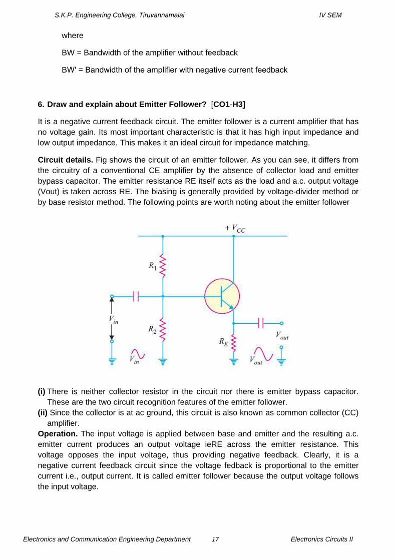
6. Draw and explain about Emitter Follower? [CO1-H3]
It is a negative current feedback circuit. The emitter follower is a current amplifier that has no voltage gain. Its most important characteristic is that it has high input impedance and low output impedance. This makes it an ideal circuit for impedance matching.
Circuit details. Fig shows the circuit of an emitter follower. As you can see, it differs from the circuitry of a conventional CE amplifier by the absence of collector load and emitter bypass capacitor. The emitter resistance RE itself acts as the load and a.c. output voltage (Vout) is taken across RE. The biasing is generally provided by voltage-divider method or by base resistor method. The following points are worth noting about the emitter follower
(i) There is neither collector resistor in the circuit nor there is emitter bypass capacitor. These are the two circuit recognition features of the emitter follower.
(ii) Since the collector is at ac ground, this circuit is also known as common collector (CC) amplifier.
Operation. The input voltage is applied between base and emitter and the resulting a.c. emitter current produces an output voltage ieRE across the emitter resistance. This voltage opposes the input voltage, thus providing negative feedback. Clearly, it is a negative current feedback circuit since the voltage fedback is proportional to the emitter current i.e., output current. It is called emitter follower because the output voltage follows the input voltage.
S.K.P. Engineering College, Tiruvannamalai IV SEM
Electronics and Communication Engineering Department 18 Electronics Circuits II
Characteristics:
The major characteristics of the emitter follower are :
(i) No voltage gain. In fact, the voltage gain of an emitter follower is close to 1. (ii) Relatively high current gain and power gain. (iii) High input impedance and low output impedance. (iv) Input and output ac voltages are in phase.
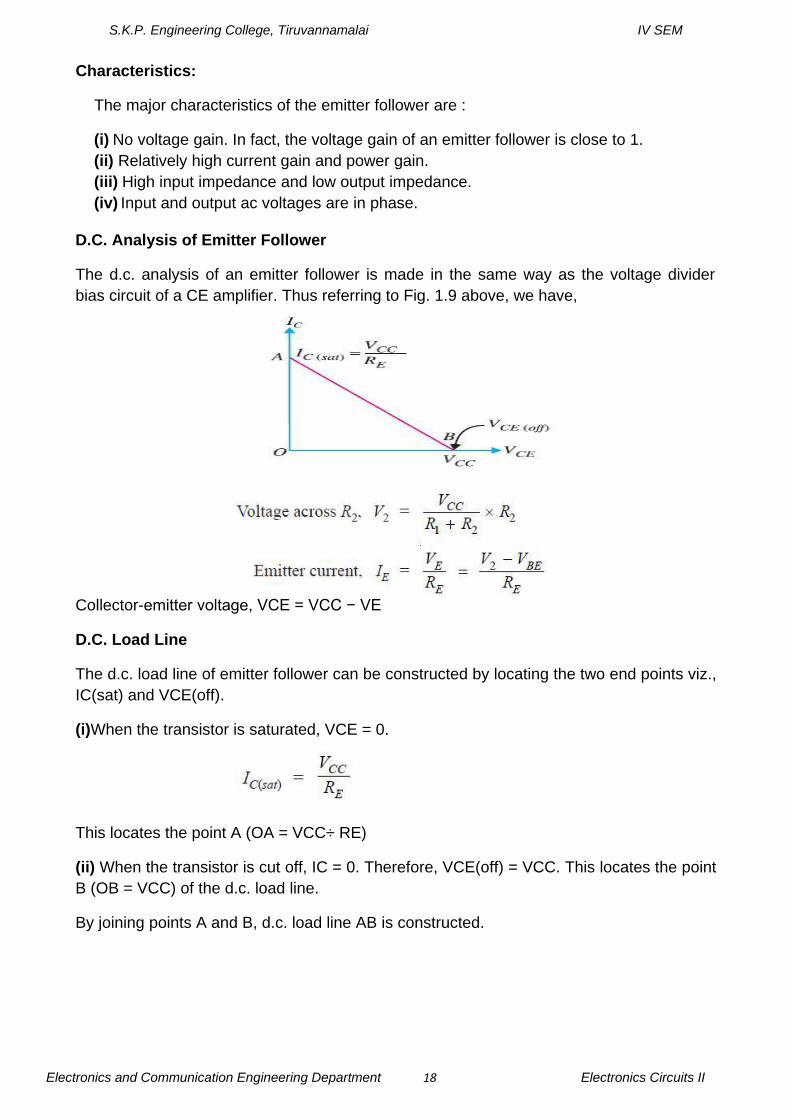
D.C. Analysis of Emitter Follower
The d.c. analysis of an emitter follower is made in the same way as the voltage divider bias circuit of a CE amplifier. Thus referring to Fig. 1.9 above, we have,
Collector-emitter voltage, VCE = VCC − VE
D.C. Load Line
The d.c. load line of emitter follower can be constructed by locating the two end points viz., IC(sat) and VCE(off).
(i)When the transistor is saturated, VCE = 0.
This locates the point A (OA = VCC÷ RE)
(ii) When the transistor is cut off, IC = 0. Therefore, VCE(off) = VCC. This locates the point B (OB = VCC) of the d.c. load line.
By joining points A and B, d.c. load line AB is constructed.

S.K.P. Engineering College, Tiruvannamalai IV SEM
Electronics and Communication Engineering Department 19 Electronics Circuits II
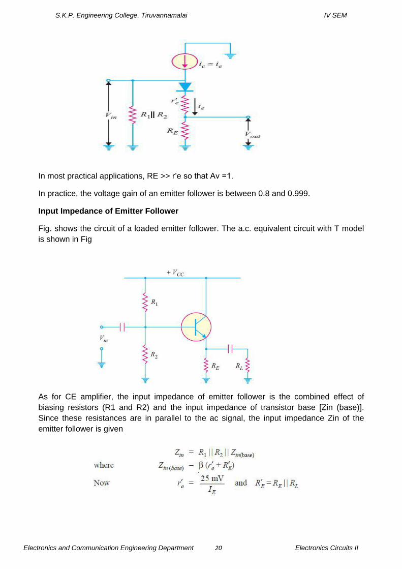
Voltage Gain of Emitter Follower
Fig. 1.11 shows the emitter follower circuit. Since the emitter resistor is not bypassed by a capacitor, the a.c. equivalent circuit of emitter follower will be as shown in Fig. 1.12. The ac resistance rE of the emitter circuit is given by
In order to find the voltage gain of the emitter follower, let us replace the transistor in Fig. 1.12 by its equivalent circuit. The circuit then becomes as shown in Fig. 1.13. Note that input voltage is applied across the ac resistance of the emitter circuit i.e., (r’e + RE). Assuming the emitter diode to be ideal,
Output voltage, Vout = ie RE
Input voltage, Vin = ie (r’e + RE)
Voltage gain of emitter follower is
S.K.P. Engineering College, Tiruvannamalai IV SEM
Electronics and Communication Engineering Department 20 Electronics Circuits II
In most practical applications, RE >> r’e so that Aν =1.
In practice, the voltage gain of an emitter follower is between 0.8 and 0.999.
Input Impedance of Emitter Follower
Fig. shows the circuit of a loaded emitter follower. The a.c. equivalent circuit with T model is shown in Fig
As for CE amplifier, the input impedance of emitter follower is the combined effect of biasing resistors (R1 and R2) and the input impedance of transistor base [Zin (base)]. Since these resistances are in parallel to the ac signal, the input impedance Zin of the emitter follower is given
S.K.P. Engineering College, Tiruvannamalai IV SEM
Electronics and Communication Engineering Department 21 Electronics Circuits II
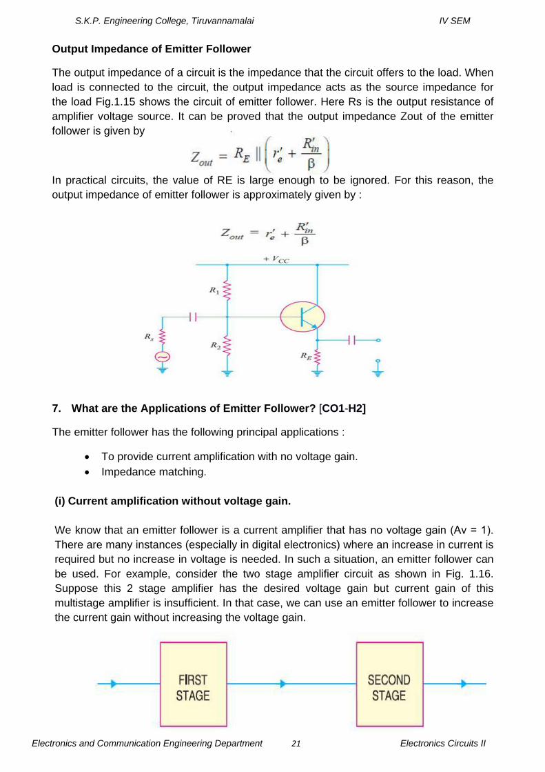
Output Impedance of Emitter Follower
The output impedance of a circuit is the impedance that the circuit offers to the load. When load is connected to the circuit, the output impedance acts as the source impedance for the load Fig.1.15 shows the circuit of emitter follower. Here Rs is the output resistance of amplifier voltage source. It can be proved that the output impedance Zout of the emitter follower is given by
In practical circuits, the value of RE is large enough to be ignored. For this reason, the output impedance of emitter follower is approximately given by :
7. What are the Applications of Emitter Follower? [CO1-H2]
The emitter follower has the following principal applications :
• To provide current amplification with no voltage gain. • Impedance matching.
(i) Current amplification without voltage gain. We know that an emitter follower is a current amplifier that has no voltage gain (Aν = 1). There are many instances (especially in digital electronics) where an increase in current is required but no increase in voltage is needed. In such a situation, an emitter follower can be used. For example, consider the two stage amplifier circuit as shown in Fig. 1.16. Suppose this 2 stage amplifier has the desired voltage gain but current gain of this multistage amplifier is insufficient. In that case, we can use an emitter follower to increase the current gain without increasing the voltage gain.
S.K.P. Engineering College, Tiruvannamalai IV SEM
Electronics and Communication Engineering Department 22 Electronics Circuits II
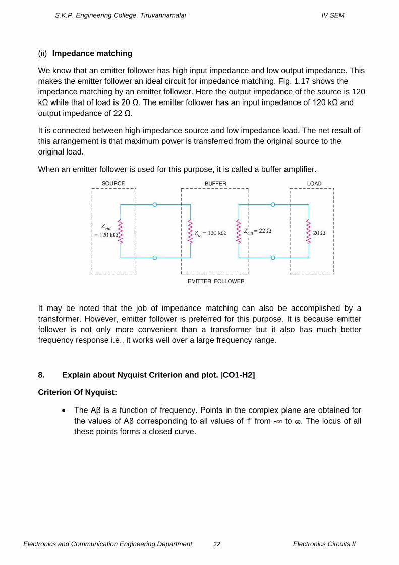
(ii) Impedance matching
We know that an emitter follower has high input impedance and low output impedance. This makes the emitter follower an ideal circuit for impedance matching. Fig. 1.17 shows the impedance matching by an emitter follower. Here the output impedance of the source is 120 kΩ while that of load is 20 Ω. The emitter follower has an input impedance of 120 kΩ and output impedance of 22 Ω.
It is connected between high-impedance source and low impedance load. The net result of this arrangement is that maximum power is transferred from the original source to the original load.
When an emitter follower is used for this purpose, it is called a buffer amplifier.
It may be noted that the job of impedance matching can also be accomplished by a transformer. However, emitter follower is preferred for this purpose. It is because emitter follower is not only more convenient than a transformer but it also has much better frequency response i.e., it works well over a large frequency range.
8. Explain about Nyquist Criterion and plot. [CO1-H2]
Criterion Of Nyquist:
• The Aβ is a function of frequency. Points in the complex plane are obtained for the values of Aβ corresponding to all values of ‘f’ from - to . The locus of all these points forms a closed curve.
S.K.P. Engineering College, Tiruvannamalai IV SEM
Electronics and Communication Engineering Department 23 Electronics Circuits II
The amplifier is unstable if this curve encloses the point –1+j0 and the amplifier is stable if the curve does not enclose this point.
S.K.P. Engineering College, Tiruvannamalai IV SEM
Electronics and Communication Engineering Department 24 Electronics Circuits II
Unit-II
Oscillators
Part-A
1. Mention two essential conditions for a circuit to maintain oscillations [CO2-L1]
The conditions for oscillator to produce oscillation are given by Barkhausan criterion. They are
• The total phase shift produced by the circuit should be 360o or 0o • The Magnitude of loop gain must be greater than or equal to 1 (ie)|Aβ|≥1
2. What is the major disadvantage of a Twin-T oscillator? [NOV/DEC 2012]
[CO2-L1] Twin –T oscillator is operated only at one frequency.
3. Differentiate oscillator from amplifier.[NOV/DEC 2013] [CO2-L2]
Oscillators
1. They are self-generating circuits. They generate waveforms like sine, square and triangular waveforms of their own. Without having input signal.
2. It have infinite gain
3. Oscillator uses positive feedback
Amplifiers
1. They are not self-generating circuits. They need a signal at the input and they just increase the level of the input waveform.
2. It have finite gain
3. Amplifier uses negative feedback.
4. State Barkhausen criterion for sustained oscillation. What will happen to the oscillation if the magnitude of the loop gain is greater than unity?[NOV/DEC 2013] [CO2-L1]
The conditions for oscillator to produce oscillation are given by Barkhausan criterion. They are :
• The total phase shift produced by the circuit should be 360o or 0o
• The Magnitude of loop gain must be greater than or equal to 1 (ie)|Aβ|≥1 In practice loop gain is kept slightily greater than unity to ensure that oscillator work even if there is a slight change in the circuit parameters.
5. Why an LC tank circuit does not produce sustained oscillations. How can this can be overcome?[NOV/DEC 2008] [CO2-L2] We know that the inductor coil has some resistance and dielectric material of the capacitor has some leakage.so small part of the originally imparted energy is used to overcome these losses. As a result, the amplitude of oscillating current goes on decreasing and becomes zero when all energy is consumed as losses. So a LC tank circuit does not produce sustained oscillations.
S.K.P. Engineering College, Tiruvannamalai IV SEM
Electronics and Communication Engineering Department 25 Electronics Circuits II
To maintain sustained oscillations, energy must be supplied to the circuit at the same rate at which it is dissipated. In an oscillator, the function of transistor and power supply source is to feed energy to the circuit to overcome the losses at right time. 6. What are the advantages and disadvantages of RC phase shift
Oscillators? [CO2-L1] • It is best suited for generating fixed frequency signals in the audio
frequency range. • It requires no transformer or inductor, hence less bulky. • Simple Circuit.
Disadvantages: • It requires a high β transistor to overcome losses in the network. • These oscillators are not suitable for high frequency operation. • Frequency of oscillation cannot be changed easily. To change the frequency of Oscillation, the three capacitor or resistors should be changed simultaneously. • This is inconvenient.
7. What is the necessary condition for a Wien bridge oscillator circuit to have sustained oscillations? [MAY/JUNE 2013] [CO2-L2]
Then for oscillations to occur in a Wien Bridge Oscillator circuit the following conditions must apply.
• With no input signal the Wien Bridge Oscillator produces output oscillations.
• The Wien Bridge Oscillator can produce a large range of frequencies. • The Voltage gain of the amplifier must be at least 3. • The network can be used with a Non-inverting amplifier. • The input resistance of the amplifier must be high compared to R so
that the RC network is not overloaded and alter the required conditions.
• The output resistance of the amplifier must be low so that the effect of external loading is minimized.
8. Define piezoelectric effect.[MAY/JUNE 2006] [CO2-L1] The piezo electric Crystals exhibit a property that if a mechanical stress is applied across one face the electric potential is developed across opposite face and viceversa. This phenomenon is called piezo electric effect.

S.K.P. Engineering College, Tiruvannamalai IV SEM
Electronics and Communication Engineering Department 26 Electronics Circuits II
9. What is the principle behind operation of a crystal oscillator? [NOV/DEC 2007] [CO2-L1] The principle behind the operation of crystal is piezoelectric effect. According to this effect, if a mechanical stress is applied across one face the electric potential is developed across opposite face and vice versa. 10. Draw an oscillator circuit with feedback network given below.[MAY/JUNE 2006] [CO2-L3]
11. What are the advantages and disadvantages of wein bridge oscillators? [CO2-L2] Advantages
1. Provides a stable low distortion sinusoidal output over a wide range of frequency.
2. The frequency range can be selected simply by using decade resistance boxes. 3. The frequency of oscillation can be easily varied by varying capacitances C1 and C2 simultaneously. The overall gain is high because of two transistors.
Disadvantages
1. The circuit needs two transistors and a large number of other components. 2. The maximum frequency output is limited because of amplitude and the phase-shift characteristics of amplifier.
Part-B
1. Write briefly about Oscillators? [CO2-H2]
An oscillator is a circuit that produces a repetitive signal from a dc voltage .The feedback type oscillator which rely on a positive feedback of the output to maintain the oscillations. The relaxation oscillator makes use of an RC timing circuit to generate a non-sinusoidal signal such as square wave.
The requirements for oscillation are described by the Baukhausen criterion:

S.K.P. Engineering College, Tiruvannamalai IV SEM
Electronics and Communication Engineering Department 27 Electronics Circuits II
The magnitude of the loop gain Aβ must be 1 The phase shift of the loop gain A β must be 0o or 360o or integer multiple of 2pi
Amplitude stabilization:
In both the oscillators above, the loop gain is set by component values In practice the gain of the active components is very variuable If the gain of the circuit is too high it will saturate If the gain of the circuit is too low the oscillation will die Real circuits need some means of stabilizing the magnitude of the oscillation to
cope with variability in the gain of the circuit
Barkhausan criterion:The conditions for oscillator to produce oscillation are given by Barkhausan criterion. They are :
• The total phase shift produced by the circuit should be 360o or 0o
• The Magnitude of loop gain must be greater than or equal to 1 (ie)|Aβ|≥1 In practice loop gain is kept slightily greater than unity to ensure that oscillator work even if there is a slight change in the circuit parameters.
2. Write the Mechanism of start of LC Oscillator. [CO2-H1]
The starting voltage is provided by noise, which is produced due to random motion of electrons in resistors used in the circuit. The noise voltage contains almost all the sinusoidal frequencies. This low amplitude noise voltage gets amplified and appears at the output terminals. The amplified noise drives the feedback network which is the phase shift network. Because of this the feedback voltage is maximum at a particular frequency, which in turn represents the frequency of oscillation.
LC Oscillator
Oscillators are used in many circuits and systems providing the central “clock” signal that controls that controls the sequential operation of the entire system. Oscillators convert a DC input (the supply voltage) into an AC output (the waveform), which can have a wide range of different wave shapes and frequencies that can be either complicated in nature or simple sine waves depending upon the application.
Oscillators are also used in many pi s of test equipment producing either sinusoidal sine wave, square, sawtooth or triangular shaped waveforms or just a train of pulse of a variable or constant width. LC Oscillators are commonly used in radio-frequency
S.K.P. Engineering College, Tiruvannamalai IV SEM
Electronics and Communication Engineering Department 28 Electronics Circuits II
circuits because of their good phase noise characteristics and their ease of implementation.
An Oscillator is basically anAmplifier with “Positive Feedback”, or regenerative feedback (in-phase) and one of the many problems in circuit design is stooping amplifiers from oscillating while trying to get oscillators to oscillate. Oscillators work because they overcome the losses of their feedback resonator circuit either in the form of a capacitor or both in the same circuit by applying DC energy at the required frequency into this resonator circuit. In other words, an oscillator is a an amplifier which uses positive feedback that generates an output frequency without the use of an input signal.
It is self sustaining. Then an oscillator has a small signal feedback amplifier with an open-loop gain equal too or slightly greater than one for oscillations to start but to continue oscillations the average loop gain must return to unity. In addition to these reactive components, an amplifying device such as an Operational Amplifier or Bipolar Transistors required. Unlike an amplifier there is no external AC input required to cause the Oscillator to work as the DC supply energy is converted by the oscillator into AC energy at the required frequency.
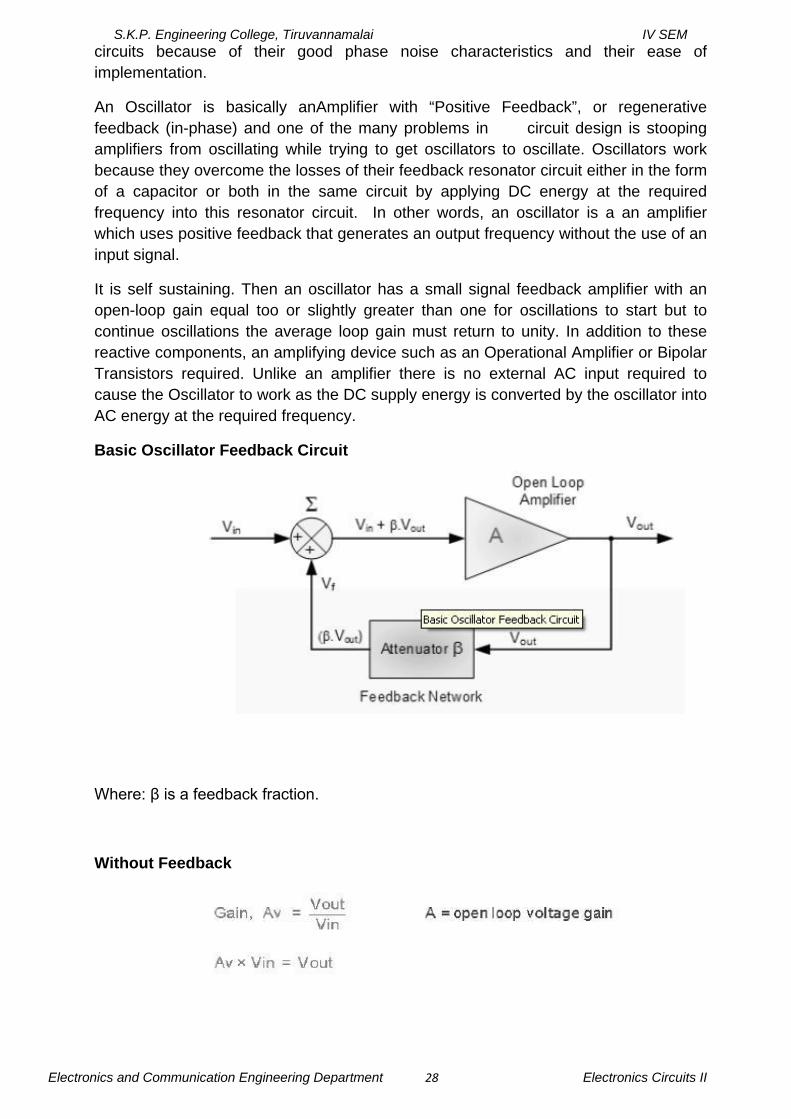
Basic Oscillator Feedback Circuit
Where: β is a feedback fraction.
Without Feedback
S.K.P. Engineering College, Tiruvannamalai IV SEM
Electronics and Communication Engineering Department 29 Electronics Circuits II
With Feedback
Oscillators are circuits that generate a continuous voltage output waveform at a required frequency with the values of the inductors, capacitors or resistors forming a frequency selective LC resonant tank circuit and feedback network. This feedback network is an attenuation network which has a gain of less than one (β<1) and starts oscillations when A β>1 which returns to unity (A β=1) once oscillations commence. The LC oscillators’ frequency is controlled using a tuned or resonant inductive/capacitive (LC) circuit with the resulting output frequency being known as the Oscillation Frequency. By making the oscillators feedback a reactive network the phase angle of the feedback will vary as a function of frequency and this is called Phase-shift. There are basically types of Oscillators:
1. Sinusoidal Oscillators - these are known as Harmonic Oscillators and are generally a LC Tuned-feedback” or “RC tuned-feedback” type Oscillator that generates a purely sinusoidal waveform which is of constant amplitude and frequency.
2. Non-Sinusoidal Oscillators – these are known as Relaxation Oscillators and generate complex non-sinusoidal waveforms that changes very quickly from one condition of stability to another such as
“Square-wave”, “Triangular-wave” or “Sawtoothed-wave” type waveforms.
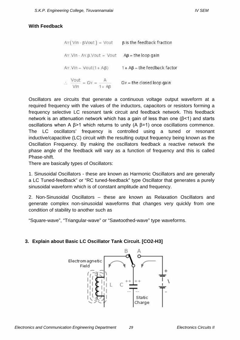
3. Explain about Basic LC Oscillator Tank Circuit. [CO2-H3]
S.K.P. Engineering College, Tiruvannamalai IV SEM
Electronics and Communication Engineering Department 30 Electronics Circuits II
The circuit consists of an inductive coil, L and a capacitor, C. The capacitor stores energy in the form of an electrostatic field and which produces a potential (static voltage) across its plates, while the inductive coil stores its energy in the form of an electromagnetic field.
The capacitor is charged up to the DC supply voltage, V by putting the switch in position A. When the capacitor is fully charged the switch changes to position B. The charged capacitor is now connected in parallel across the inductive coil so the capacitor begins to discharge itself through the coil.
The voltage across C starts falling as the current through the coil begins to rise. This rising current sets up an electromagnetic field around the coil which resists this flow of current. When the capacitor, C is completely discharged the energy that was originally stored in the capacitor, C as an electrostatic filed is now stored in the inductive coil, L as an electromagnetic field around the coils windings.
As there is now no external voltage in the circuit to maintain the current within the coil, it starts to fall as the electromagnetic field begins to collapse. A back emf is induced in the coil (e= -Ldi/dt) keeping the current flowing in the original direction. This current now charges up the capacitor, c with the opposite polarity to its original charge C continues to chare up until the current reduces to zero and the electromagnetic field of the coil has collapsed completely. The energy originally introduced into the circuit through the switch, has been returned to the capacitor which again has an electrostatic voltage potential across it, although it is now of the opposite polarity. The capacitor now starts to discharge again back through the coil and the whole process os repeated. The polarity of the voltage changes as the energy is passed back and forth between the capacitor and inductor producing an AC type sinusoidal voltage and current waveform.
This then forms the basis of an LC oscillators tank circuit and theoretically this cycling back and forth will continue indefinitely. However, every time energy is transferred from C to L or from L to C losses occur which decay the oscillations.This oscillatory action of passing energy back and forth between the capacitor, C to the inductor, L would continue indefinitely if it was not for energy losses within the circuit. Electrical energy is lost in the DC or real resistance of the inductors coil, in the dielectric of the capacitor, and in radiation from the circuit so the oscillation steadily decreases until they die away completely and the process stops.
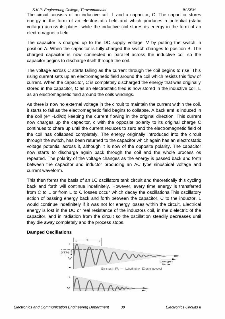
Damped Oscillations

S.K.P. Engineering College, Tiruvannamalai IV SEM
Electronics and Communication Engineering Department 31 Electronics Circuits II
The frequency of the oscillatory voltage depends upon the value of the inductance and capacitance in the LC tank circuit. We now know that for resonance to occur in the tank circuit, there must be a frequency point were the value of XC, the capacitive reactance is the same as the value of XL, the inductive reactance (XL = XC) and which will therefore cancel out each other out leaving only the DC resistance in the circuit to oppose the flow of current.
If we now place the curve for inductive reactance on top of the curve for capacitive reactance so that both curves are on the same axes, the point of intersection will give us the resonance frequency point, ( ƒr or ωr ) as shown below.
Resonance Frequency
where: ƒr is in Hertz, L is in Henries and C is in Farads.
Then the frequency at which this will happen is given as
Then by simplifying the above equation we get the final equation for Resonant Frequency.
S.K.P. Engineering College, Tiruvannamalai IV SEM
Electronics and Communication Engineering Department 44 Electronics Circuits II
4. Explain the concepts of Hartley Oscillator? [CO2-H2]
The main disadvantages of the basic LC Oscillator circuit we looked at in the previous tutorial is that they have no means of controlling the amplitude of the oscillations and also, it is difficult to tune the oscillator to the required frequency.
If the cumulative electromagnetic coupling between L1 and L2 is too small there would be insufficient feedback and the oscillations would eventually die away to zero.
However, it is possible to feed back exactly the right amount of voltage for constant amplitude oscillations. If we feed back more than is n ssary the amplitude of the oscillations can be controlled by biasing the amplifier in such a way that if the oscillations increase in amplitude, the bias is increased and the gain of the amplifier is reduced.
If the amplitude of the oscillations decreases the bias decreases and the gain of the amplifier increases, thus increasing the feedback. In this way the amplitude of the oscillations are kept constant using a process known as Automatic Base Bias.
One big advantage of automatic base bias in a voltage controlled oscillator, is that the oscillator can be made more efficient by providing a Class-B bias or even a Class-C bias condition of the transistor. This has the advantage that the collector current only flows during part of the oscillation cycle so the quie nt collector current is very small.
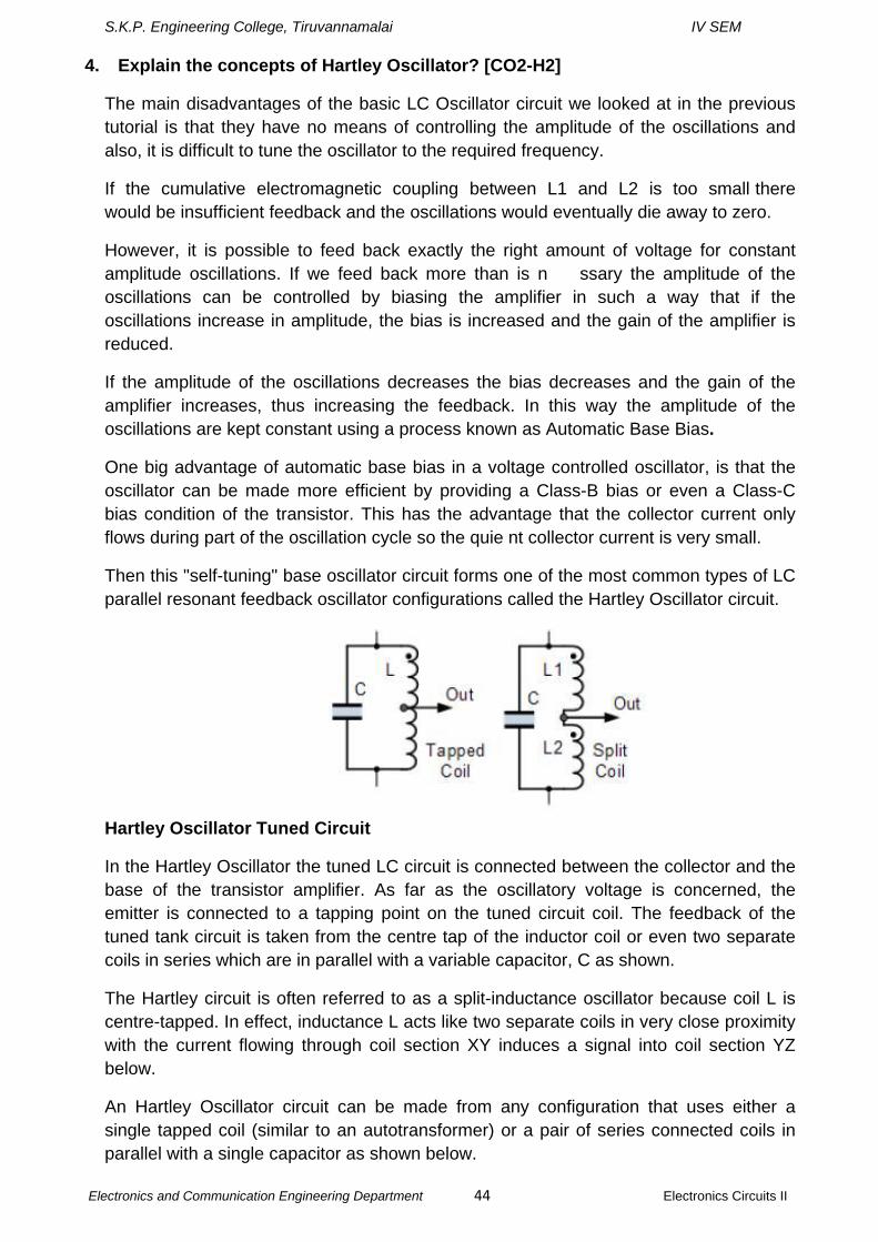
Then this "self-tuning" base oscillator circuit forms one of the most common types of LC parallel resonant feedback oscillator configurations called the Hartley Oscillator circuit.
Hartley Oscillator Tuned Circuit
In the Hartley Oscillator the tuned LC circuit is connected between the collector and the base of the transistor amplifier. As far as the oscillatory voltage is concerned, the emitter is connected to a tapping point on the tuned circuit coil. The feedback of the tuned tank circuit is taken from the centre tap of the inductor coil or even two separate coils in series which are in parallel with a variable capacitor, C as shown.
The Hartley circuit is often referred to as a split-inductance oscillator because coil L is centre-tapped. In effect, inductance L acts like two separate coils in very close proximity with the current flowing through coil section XY induces a signal into coil section YZ below.
An Hartley Oscillator circuit can be made from any configuration that uses either a single tapped coil (similar to an autotransformer) or a pair of series connected coils in parallel with a single capacitor as shown below.
S.K.P. Engineering College, Tiruvannamalai IV SEM
Electronics and Communication Engineering Department 45 Electronics Circuits II
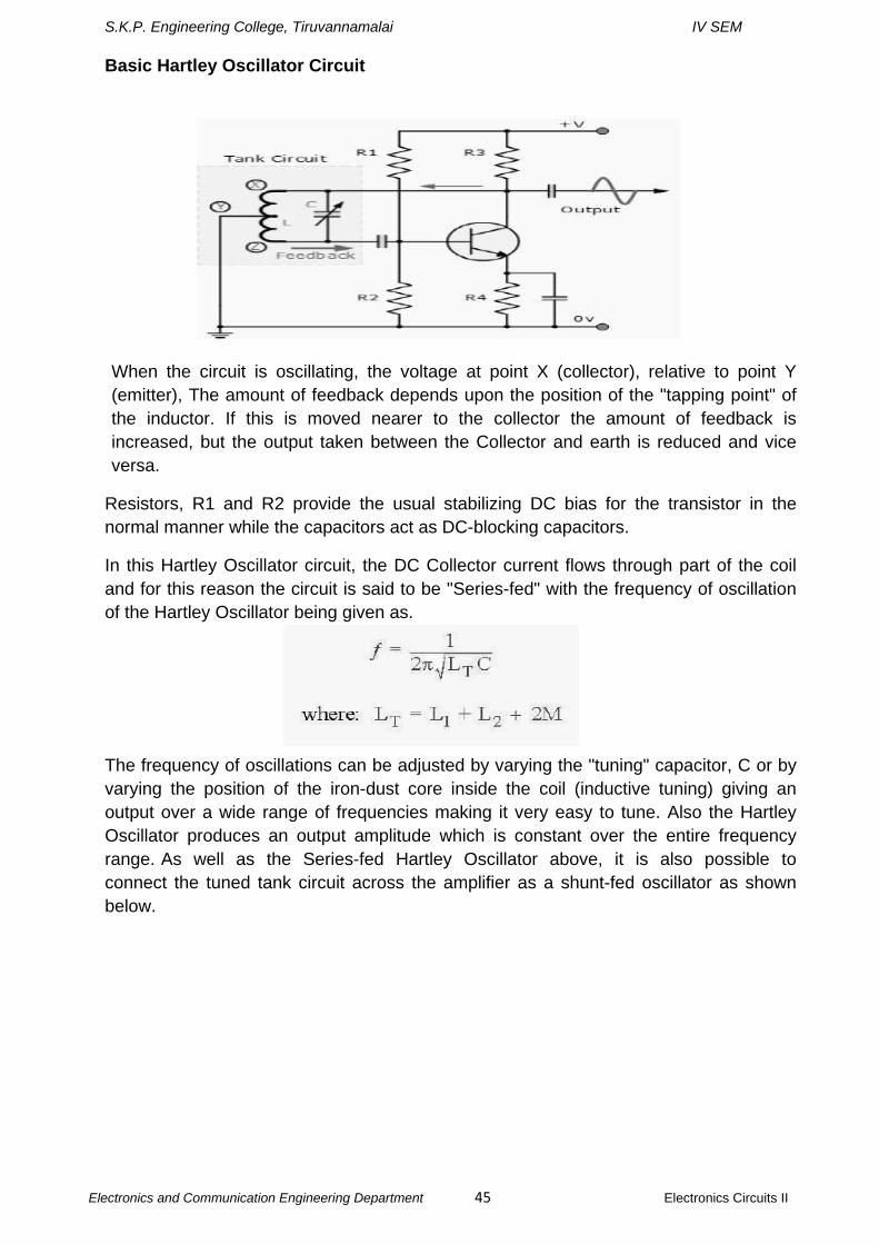
Basic Hartley Oscillator Circuit
When the circuit is oscillating, the voltage at point X (collector), relative to point Y (emitter), The amount of feedback depends upon the position of the "tapping point" of the inductor. If this is moved nearer to the collector the amount of feedback is increased, but the output taken between the Collector and earth is reduced and vice versa.
Resistors, R1 and R2 provide the usual stabilizing DC bias for the transistor in the normal manner while the capacitors act as DC-blocking capacitors.
In this Hartley Oscillator circuit, the DC Collector current flows through part of the coil and for this reason the circuit is said to be "Series-fed" with the frequency of oscillation of the Hartley Oscillator being given as.
The frequency of oscillations can be adjusted by varying the "tuning" capacitor, C or by varying the position of the iron-dust core inside the coil (inductive tuning) giving an output over a wide range of frequencies making it very easy to tune. Also the Hartley Oscillator produces an output amplitude which is constant over the entire frequency range. As well as the Series-fed Hartley Oscillator above, it is also possible to connect the tuned tank circuit across the amplifier as a shunt-fed oscillator as shown below.
S.K.P. Engineering College, Tiruvannamalai IV SEM
Electronics and Communication Engineering Department 46 Electronics Circuits II
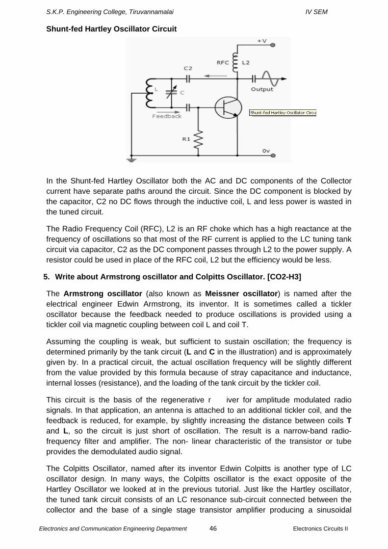
Shunt-fed Hartley Oscillator Circuit
In the Shunt-fed Hartley Oscillator both the AC and DC components of the Collector current have separate paths around the circuit. Since the DC component is blocked by the capacitor, C2 no DC flows through the inductive coil, L and less power is wasted in the tuned circuit.
The Radio Frequency Coil (RFC), L2 is an RF choke which has a high reactance at the frequency of oscillations so that most of the RF current is applied to the LC tuning tank circuit via capacitor, C2 as the DC component passes through L2 to the power supply. A resistor could be used in place of the RFC coil, L2 but the efficiency would be less.
5. Write about Armstrong oscillator and Colpitts Oscillator. [CO2-H3]
The Armstrong oscillator (also known as Meissner oscillator) is named after the electrical engineer Edwin Armstrong, its inventor. It is sometimes called a tickler oscillator because the feedback needed to produce oscillations is provided using a tickler coil via magnetic coupling between coil L and coil T.
Assuming the coupling is weak, but sufficient to sustain oscillation; the frequency is determined primarily by the tank circuit (L and C in the illustration) and is approximately given by. In a practical circuit, the actual oscillation frequency will be slightly different from the value provided by this formula because of stray capacitance and inductance, internal losses (resistance), and the loading of the tank circuit by the tickler coil.
This circuit is the basis of the regenerative r iver for amplitude modulated radio signals. In that application, an antenna is attached to an additional tickler coil, and the feedback is reduced, for example, by slightly increasing the distance between coils T and L, so the circuit is just short of oscillation. The result is a narrow-band radio-frequency filter and amplifier. The non- linear characteristic of the transistor or tube provides the demodulated audio signal.
The Colpitts Oscillator, named after its inventor Edwin Colpitts is another type of LC oscillator design. In many ways, the Colpitts oscillator is the exact opposite of the Hartley Oscillator we looked at in the previous tutorial. Just like the Hartley oscillator, the tuned tank circuit consists of an LC resonance sub-circuit connected between the collector and the base of a single stage transistor amplifier producing a sinusoidal
S.K.P. Engineering College, Tiruvannamalai IV SEM
Electronics and Communication Engineering Department 47 Electronics Circuits II
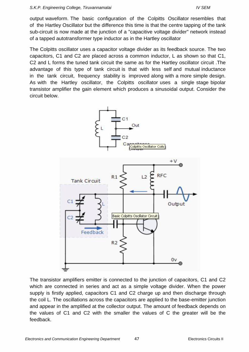
output waveform. The basic configuration of the Colpitts Oscillator resembles that of the Hartley Oscillator but the difference this time is that the centre tapping of the tank sub-circuit is now made at the junction of a "capacitive voltage divider" network instead of a tapped autotransformer type inductor as in the Hartley oscillator
The Colpitts oscillator uses a capacitor voltage divider as its feedback source. The two capacitors, C1 and C2 are placed across a common inductor, L as shown so that C1, C2 and L forms the tuned tank circuit the same as for the Hartley oscillator circuit .The advantage of this type of tank circuit is that with less self and mutual inductance in the tank circuit, frequency stability is improved along with a more simple design. As with the Hartley oscillator, the Colpitts oscillator uses a single stage bipolar transistor amplifier the gain element which produces a sinusoidal output. Consider the circuit below.
The transistor amplifiers emitter is connected to the junction of capacitors, C1 and C2 which are connected in series and act as a simple voltage divider. When the power supply is firstly applied, capacitors C1 and C2 charge up and then discharge through the coil L. The oscillations across the capacitors are applied to the base-emitter junction and appear in the amplified at the collector output. The amount of feedback depends on the values of C1 and C2 with the smaller the values of C the greater will be the feedback.

S.K.P. Engineering College, Tiruvannamalai IV SEM
Electronics and Communication Engineering Department 48 Electronics Circuits II
The required external phase shift is obtained in a similar manner to that in the Hartley oscillator circuit with the required positive feedback obtained for sustained un-damped oscillations. The amount of feedback is determined by the ratio of C1 and C2 which are generally "ganged" together to provide a constant amount of feedback so as one is adjusted the other automatically follows.
The frequency of oscillations for a Colpitts oscillator is determined by the resonant frequency of the LC tank circuit and is given as:
where CT is the capacitance of C1 and C2 connected in series and is given as:.
The configuration of the transistor amplifier is of a Common Emitter Amplifier with the output signal 180o out of phase with regards to the input signal. The additional 180o phase shift require for oscillation is achieved by the fact that the two capacitors are connected together in series but in parallel with the inductive coil resulting in overall phase shift of the circuit being zero or 360o.
Resistors, R1 and R2 provide the usual stabilizing DC bias for the transistor in the normal manner while the capacitor acts as a DC-blocking capacitors. The radio-frequency choke (RFC) is used to provide a high reactance (ideally open circuit) at the frequency of oscillation ( ƒr )
6. Explain about RC Phase-Shift Oscillator. [CO2-H2]
In a RC Oscillator the input is shifted 180o through the amplifier stage and180o again through a second inverting stage giving us "180o + 180o = 360o" of phase shift which is the same as 0o thereby giving us the required positive feedback. In other words, the phase shift of the feedback loop should be "0".
In a Resistance-Capacitance Oscillator or simply an RC Oscillator, we make use of the fact that a phase shift occurs between the input to a RC network and the output from the same network by using RC elements in the feedback branch.
S.K.P. Engineering College, Tiruvannamalai IV SEM
Electronics and Communication Engineering Department 49 Electronics Circuits II
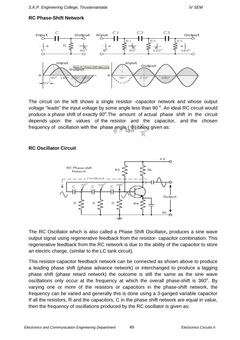
RC Phase-Shift Network
The circuit on the left shows a single resistor -capacitor network and whose output voltage "leads" the input voltage by some angle less than 90 o. An ideal RC circuit would produce a phase shift of exactly 90o.The amount of actual phase shift in the circuit depends upon the values of the resistor and the capacitor, and the chosen frequency of oscillation with the phase angle ( Φ) being given as:
RC Oscillator Circuit
The RC Oscillator which is also called a Phase Shift Oscillator, produces a sine wave output signal using regenerative feedback from the resistor- capacitor combination. This regenerative feedback from the RC network is due to the ability of the capacitor to store an electric charge, (similar to the LC tank circuit).
This resistor-capacitor feedback network can be connected as shown above to produce a leading phase shift (phase advance network) or interchanged to produce a lagging phase shift (phase retard network) the outcome is still the same as the sine wave oscillations only occur at the frequency at which the overall phase-shift is 360o. By varying one or more of the resistors or capacitors in the phase-shift network, the frequency can be varied and generally this is done using a 3-ganged variable capacitor If all the resistors, R and the capacitors, C in the phase shift network are equal in value, then the frequency of oscillations produced by the RC oscillator is given as:
S.K.P. Engineering College, Tiruvannamalai IV SEM
Electronics and Communication Engineering Department 50 Electronics Circuits II
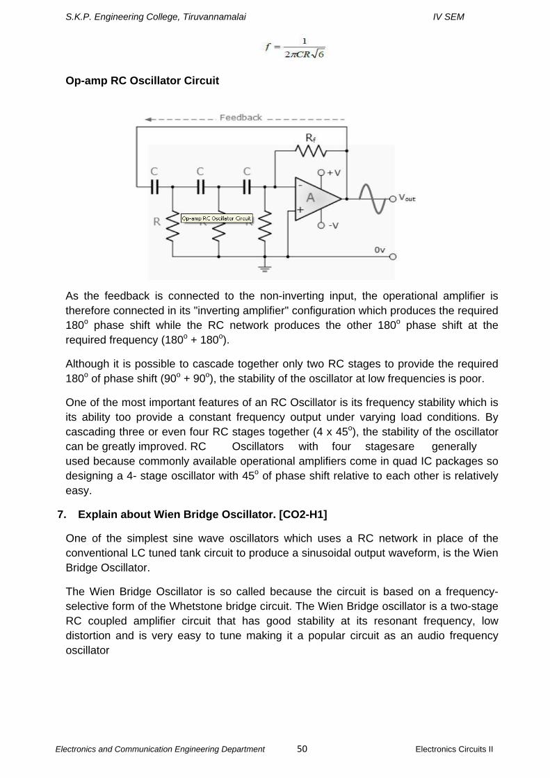
Op-amp RC Oscillator Circuit
As the feedback is connected to the non-inverting input, the operational amplifier is therefore connected in its "inverting amplifier" configuration which produces the required 180o phase shift while the RC network produces the other 180o phase shift at the required frequency (180o + 180o).
Although it is possible to cascade together only two RC stages to provide the required 180o of phase shift (90o + 90o), the stability of the oscillator at low frequencies is poor.
One of the most important features of an RC Oscillator is its frequency stability which is its ability too provide a constant frequency output under varying load conditions. By cascading three or even four RC stages together (4 x 45o), the stability of the oscillator can be greatly improved. RC Oscillators with four stages are generally used because commonly available operational amplifiers come in quad IC packages so designing a 4- stage oscillator with 45o of phase shift relative to each other is relatively easy.
7. Explain about Wien Bridge Oscillator. [CO2-H1]
One of the simplest sine wave oscillators which uses a RC network in place of the conventional LC tuned tank circuit to produce a sinusoidal output waveform, is the Wien Bridge Oscillator.
The Wien Bridge Oscillator is so called because the circuit is based on a frequency-selective form of the Whetstone bridge circuit. The Wien Bridge oscillator is a two-stage RC coupled amplifier circuit that has good stability at its resonant frequency, low distortion and is very easy to tune making it a popular circuit as an audio frequency oscillator
S.K.P. Engineering College, Tiruvannamalai IV SEM
Electronics and Communication Engineering Department 51 Electronics Circuits II
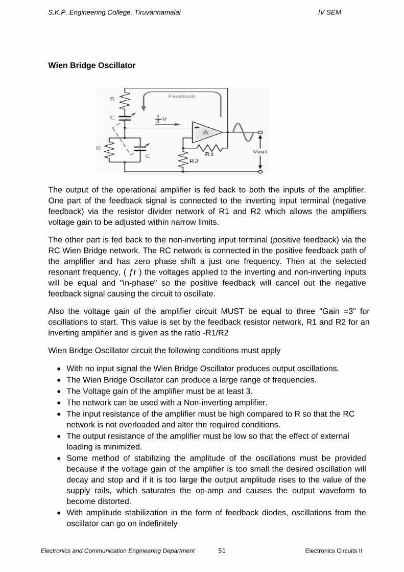
Wien Bridge Oscillator
The output of the operational amplifier is fed back to both the inputs of the amplifier. One part of the feedback signal is connected to the inverting input terminal (negative feedback) via the resistor divider network of R1 and R2 which allows the amplifiers voltage gain to be adjusted within narrow limits.
The other part is fed back to the non-inverting input terminal (positive feedback) via the RC Wien Bridge network. The RC network is connected in the positive feedback path of the amplifier and has zero phase shift a just one frequency. Then at the selected resonant frequency, ( ƒr ) the voltages applied to the inverting and non-inverting inputs will be equal and "in-phase" so the positive feedback will cancel out the negative feedback signal causing the circuit to oscillate.
Also the voltage gain of the amplifier circuit MUST be equal to three "Gain =3" for oscillations to start. This value is set by the feedback resistor network, R1 and R2 for an inverting amplifier and is given as the ratio -R1/R2
Wien Bridge Oscillator circuit the following conditions must apply
• With no input signal the Wien Bridge Oscillator produces output oscillations. • The Wien Bridge Oscillator can produce a large range of frequencies. • The Voltage gain of the amplifier must be at least 3. • The network can be used with a Non-inverting amplifier. • The input resistance of the amplifier must be high compared to R so that the RC
network is not overloaded and alter the required conditions. • The output resistance of the amplifier must be low so that the effect of external
loading is minimized. • Some method of stabilizing the amplitude of the oscillations must be provided
because if the voltage gain of the amplifier is too small the desired oscillation will decay and stop and if it is too large the output amplitude rises to the value of the supply rails, which saturates the op-amp and causes the output waveform to become distorted.
• With amplitude stabilization in the form of feedback diodes, oscillations from the oscillator can go on indefinitely
S.K.P. Engineering College, Tiruvannamalai IV SEM
Electronics and Communication Engineering Department 52 Electronics Circuits II
8. Describe about Quartz Crystal Oscillators. [CO2-H3]
One of the most important features of any oscillator is its frequency stability, or in other words its ability to provide a constant frequency output under varying load conditions. Some of the factors that affect the frequency stability of an oscillator include: temperature, variations in the load and changes in the DC power supply.
Frequency stability of the output signal can be improved by the proper selection of the components used for the resonant feedback circuit including the amplifier but there is a limit to the stability that can be obtained from normal LC and RC tank circuits.
To obtain a very high level of oscillator stability a Quartz Crystalis generally used as the frequency determining device to produce another types of oscillator circuit known generally as a Quartz Crystal Oscillator, (XO).
When a voltage source is applied to a small thin pi of quartz crystal, it begins to change shape producing a characteristic known as the Piezo-electric effect.
This piezo-electric effect is the property of a crystal by which an electrical charge produces a mechanical force by changing the shape of the crystal and vice versa, a mechanical force applied to the crystal produces an electrical charge.
Then, piezo-electric devices can be classed as Transducersas they convert energy of one kind into energy of another (electrical to mechanical or mechanical to electrical).
This piezo-electric effect produces mechanical vibrations or oscillations which are used to replace the LC tank circuit in the previous oscillators. There are many different types of crystal substances which can be used as oscillators with the most important of these for circuits being the quartz minerals because of their greater mechanical strength.
The quartz crystal used in a Quartz Crystal Oscillator is a very small, thin pi or wafer of cut quartz with the two parallel surfaces metalized to make the required electrical connections. The physical size and thickness of a pi of quartz crystal is tightly controlled since it affects the final frequency of oscillations and is called the crystals "characteristic frequency". Then once cut and shaped, the crystal can not be used at any other frequency. In other words, its size and shape determines its frequency. The crystals characteristic or resonant frequency is inversely proportional to its physical thickness between the two metalized surfaces. A mechanically vibrating crystal can be represented by an equivalent electrical circuit consisting of low resistance, large inductance and small capacitance as shown below.
S.K.P. Engineering College, Tiruvannamalai IV SEM
Electronics and Communication Engineering Department 53 Electronics Circuits II
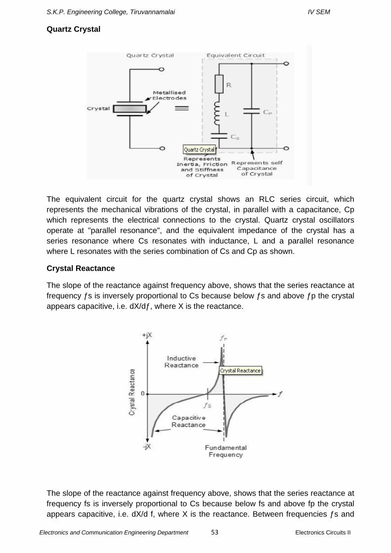
Quartz Crystal
The equivalent circuit for the quartz crystal shows an RLC series circuit, which represents the mechanical vibrations of the crystal, in parallel with a capacitance, Cp which represents the electrical connections to the crystal. Quartz crystal oscillators operate at "parallel resonance", and the equivalent impedance of the crystal has a series resonance where Cs resonates with inductance, L and a parallel resonance where L resonates with the series combination of Cs and Cp as shown.
Crystal Reactance
The slope of the reactance against frequency above, shows that the series reactance at frequency ƒs is inversely proportional to Cs because below ƒs and above ƒp the crystal appears capacitive, i.e. dX/dƒ, where X is the reactance.
The slope of the reactance against frequency above, shows that the series reactance at frequency fs is inversely proportional to Cs because below fs and above fp the crystal appears capacitive, i.e. dX/d f, where X is the reactance. Between frequencies ƒs and

S.K.P. Engineering College, Tiruvannamalai IV SEM
Electronics and Communication Engineering Department 54 Electronics Circuits II
ƒp, the crystal app ears inductive as the two parallel capacitances cancel out. The point where the reactance values of the capacitances and inductance cancel each other out Xc = XL is the fundamental frequency of the crystal. A quartz crystal has a resonant frequency similar to that of a electrically tuned tank circuit butwith a much higher Q factor due to its low resistance, with typical frequencies ranging from 4kHz to 10MHz.
The cut of the crystal also determines how it will behave as some crystals will vibrate at more than one frequency. Also, if the crystal is not of a parallel or uniform thickness it has two or more resonant frequencies having both a fundamental frequency and harmonics such as second or third harmonics. However, usually the fundamental frequency is more stronger or pronounced than the others and this is the one used. The equivalent circuit above has three reactive components and there are two resonant frequencies, the lowest is a series type frequency and the highest a parallel type resonant frequency.
Colpitts Crystal Oscillator:
The design of a Crystal Oscillator is very similar to the design of the Colpitts Oscillator we looked at in the previous tutorial, except that the LC tank circuit has been replaced by a quartz crystal as shown below.
These types of Crystal Oscillators are designed around the common emitter amplifier stage of a Colpitts Oscillator. The input signal to the base of the transistor is inverted at the transistors output. The output signal at the collector is then taken through a 180o phase shifting network which includes the crystal operating in a series resonant mode. The output is also fed back to the input which is "in-phase"
Pierce Oscillator
The Pierce oscillator is a crystal oscillator that uses the crystal as part of its feedback path and therefore has no resonant tank circuit. The Pierce Oscillator uses a JFET as its amplifying device as it provides a very high input impedance with the crystal connected between the output Drain terminal and the input Gate terminal as shown below.

S.K.P. Engineering College, Tiruvannamalai IV SEM
Electronics and Communication Engineering Department 55 Electronics Circuits II
Pierce Crystal Oscillator
In this simple circuit, the crystal determines the frequency of oscillations and operates on its series resonant frequency giving a low impedance path between output and input. There is a 180° phase shift at resonance, making the feedback positive. The amplitude of the output sine wave is limited to the maximum voltage range at the Drain terminal.
Resistor, R1 controls the amount of feedback and crystal drive while the voltage across the radio frequency choke RFC reverses during each cycle. Most digital clocks, watches and timers use a Pierce Oscillator in some form or other as it can be implemented using the minimum of components.
S.K.P. Engineering College, Tiruvannamalai IV SEM
Electronics and Communication Engineering Department 56 Electronics Circuits II
UNIT III
TUNED AMPLIFIERS
Part-A
1. What is tuned amplifier? What are the various types of tuned amplifiers? [CO3-L1]
A tuned amplifier amplifies a certain range of frequencies (narrow band of frequencies) in the radio frequency region and rejects all other frequencies.
Types:
The various types of tuned amplifiers are
i) Single tuned amplifier ii) Double tuned amplifier iii) Stagger tuned amplifier & synchronously tuned amplifier.
2. Define tuned amplifier. [CO3-L2]
A tuned amplifier is defined as an amplifier circuit which amplifies a certain range of frequencies (narrow band of frequencies) in the radio frequency region and rejects all other frequencies
3. Why tuned amplifier cannot be used at low frequency? [CO3-L1]
For low frequencies the size L and C are large. So the circuit will be bulky and expensive, hence the tuned amplifiers cannot be used at low frequency.
4. What is the other name for tuned amplifier? [CO3-L1]
Tuned amplifiers used for amplifying narrow band of frequencies hence it si also known as “narrow band amplifier” or “Band pass amplifier”.
5. Mention The Two Applications of tuned amplifiers.[ NOV/DEC 2007, NOV/DEC 2008] [CO3-L1]
i) They are used in IF amplifiers in Radio and TV receivers. ii) They are used in wireless communication systems.
6. State two advantages and two disadvantages of tuned amplifiers.
[MAY/JUNE 2012] [CO3-L2]
Advantages:
i) They amplify defined frequencies ii) Signal to noise ratio (SNR) at output is good. iii) They are suited for radio transmitters and receivers.
S.K.P. Engineering College, Tiruvannamalai IV SEM
Electronics and Communication Engineering Department 57 Electronics Circuits II
Disadvantages:
i) They are not suitable to amplify audio frequencies. ii) Circuit is bulky and costly. iii) The design is complex.
7. What is Single tuned and double tuned amplifier? [CO3-L1] A amplifier circuit that uses a single parallel tuned circuit as a load is called single tuned amplifier.
Double tuned amplifier
The amplifiers having two parallel resonant circuit in its load are called double tuned amplifiers.
8. What are the advantages of double tuned amplifier over single tuned amplifier? [CO3-L1]
i) Provides higher gain ii) Provides large 3dB bandwidth. iii) Possess flatter response having steeper sides.
9. What are the different coil losses? [CO3-L1]
• Hysteresis loss • Copper loss • Eddy current loss
10. What is Stagger tuned amplifier. [CO3-L2]
If two or more tuned circuits which are cascaded are tuned to slightly different resonant frequencies, it is possible to obtain an increased bandwidth with a flat passbandwith steep sides. This technique is known as stagger tuning and the amplifier using this technique is called as stagger tuned amplifier.
11. What are the different types of neutralization? [CO3-L1]
• Hazeltine neutralization • Neutrodyne neutralization • Rice neutralization
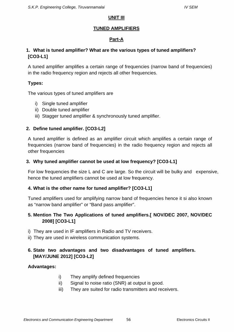
12. Why neutralization required in tuned amplifiers?[NOV/DEC 2013,NOV/DEC 2010]& Draw the circuit for Narrow Band neutralization.[NOV/DEC 2010] [CO3-L1]
In order to prevent oscillations in tuned RF amplifiers it was n ssary to reduce the stage gain to a level that ensured circuit stability. This can be accomplished in several ways such as lowering the Q of the tuned circuits, stagger tuning ,loose coupling between the stages. Instead of losingthe circuit performance to achieve stability, a circuitin which the troublesome effect of the collector to base capacitance of the
S.K.P. Engineering College, Tiruvannamalai IV SEM
Electronics and Communication Engineering Department 58 Electronics Circuits II
transistor was neutralised by introducing a signal which cancels the signal coupled through the collector to base capacitance.
13. Define loaded and unloaded Q. [CO3-L3]
It is defined as the ratio of stored energy to dissipated energy in a reactor or resonator. For an inductor or capacitor
Where X= reactance: Rs= series resistance
Loaded Q:
The loaded Q or QL of a resonator is determined by how tightly the resonator is coupled to its terminations.
14. What is the effect of cascading n stages of identical single tuned amplifiers (synchronously tuned) on the overall 3db bandwidth?[APRIL/MAY 2011] [CO3-L1]
The bandwidth of n stage cascaded single tuned amplifier is given as
From the above equation it is clear that the overall 3dB bandwidth reduces.
S.K.P. Engineering College, Tiruvannamalai IV SEM
Electronics and Communication Engineering Department 59 Electronics Circuits II
15. Mention the bandwidth of a double tuned amplifier. [CO3-L2]
Where is the resonance frequency in cycle/sec Q is the Quality factor of
the coil alone b- is a constant
16. Where is the Q-point placed in a class C type amplifier? What are its applications?[APR/MAY 2008] [CO3-L3]
In a class C type amplifier the Q-point is placed below the X-axis.
Applications:
• The Class C amplifiers are used to amplify the signals at radio frequencies. • They are also used in mixer circuits.
17. Brief the relation between bandwidth and Q-factor.[ MAY/JUNE 2007] [CO3-L1]
The quality factor determines the 3dB bandwidth for the resonant circuit. The 3dB bandwidth for resonant circuit is given by
Where fr= centre frequency of a resonator
BW= f2-f1
If Q is large bandwidth is small.If Q is small bandwidth is large.
18. What is narrow band neutralization? [APR/MAY 2008,APRIL/MAY 2011, NOV/DEC 2012] [CO3-L2]
The process of cancelling the instability effect due to the collector to base capacitance of the transistor in tuned circuits by introducing a signal which cancels the signal coupled through the collector to base capacitance is called narrow band neutralization.
19. Mention two important features of stagger tuned amplifier. [MAY/JUNE 2013] [CO3-L1]
• It has better flat, wide band characteristics. • Increased bandwidth
20. What is the need for neutralization circuits? [MAY/JUNE 2013, NOV/DEC
2008] [CO3-L2]
In tuned RF amplifiers, the inter-junction capacitance Cbc of the transistor becomes dominant (i.e) its reactance is low, it provides the feedback signal from collector to base.
S.K.P. Engineering College, Tiruvannamalai IV SEM
Electronics and Communication Engineering Department 60 Electronics Circuits II
If some feedback signal manages to reach the input from output in a positive manner with proper phase shift, then amplifier keeps oscillating, thus stability of amplifier gets affected. Hence neutralization is employed.
22. Draw a class C tuned amplifier circuit and what is its efficiency.[ MAY/JUNE 2006] [CO3-L2]
At conduction angle , η =78.5%
23. Derive the resonance frequency for the tank circuit shown:[NOV/DEC 2006] [CO3-L1]
At resonance XL=XC
Part-B
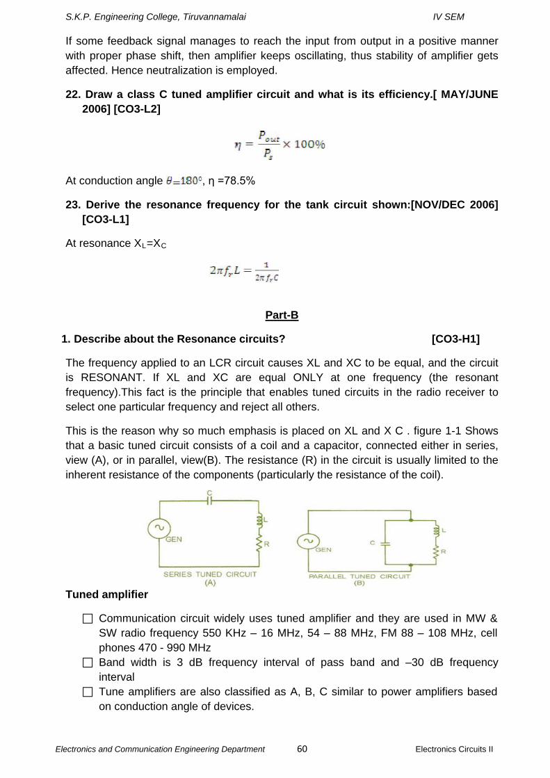
1. Describe about the Resonance circuits? [CO3-H1]
The frequency applied to an LCR circuit causes XL and XC to be equal, and the circuit is RESONANT. If XL and XC are equal ONLY at one frequency (the resonant frequency).This fact is the principle that enables tuned circuits in the radio receiver to select one particular frequency and reject all others.
This is the reason why so much emphasis is placed on XL and X C . figure 1-1 Shows that a basic tuned circuit consists of a coil and a capacitor, connected either in series, view (A), or in parallel, view(B). The resistance (R) in the circuit is usually limited to the inherent resistance of the components (particularly the resistance of the coil).
Tuned amplifier
Communication circuit widely uses tuned amplifier and they are used in MW & SW radio frequency 550 KHz – 16 MHz, 54 – 88 MHz, FM 88 – 108 MHz, cell phones 470 - 990 MHz
Band width is 3 dB frequency interval of pass band and –30 dB frequency interval
Tune amplifiers are also classified as A, B, C similar to power amplifiers based on conduction angle of devices.
S.K.P. Engineering College, Tiruvannamalai IV SEM
Electronics and Communication Engineering Department 61 Electronics Circuits II
Series resonant circuit
Series resonant features minimum impedance (RS) at resonant
f r = ½ √LC; q = L/Rs at resonance L=1/c, BW=fr/Q It behaves as purely resistance at resonance, capacitive below and inductive
above resonance Parallel resonant circuit
Parallel resonance features maximum impedance at resonance = L/RsC
At resonance Fr=1/2√1/(LC-Rs2/L2); if Rs=0, fr=1/2√(LC) At resonance it exhibits pure resistance and below fr parallel circuit
exhibits inductive and above capacitive impedance Need for tuned circuits:
To understand tuned circuits, we first have to understand the phenomenon of self-induction. And to understand this, we need to know about induction. The first discovery about the interaction between electric current and magnetism was the realization that an electric current created a magnetic field around the conductor. It was then discovered that this effect could be enhanced greatly by winding the conductor into a coil. The effect proved to be two-way: If a conductor, maybe in the form of a coil was placed in a changing magnetic field, a current could be made to flow in it; this is called induction.
So imagine a coil, and imagine that we apply a voltage to it. As current starts to flow, a magnetic field is created. But this means that our coil is in a changing magnetic field, and this induces a current in the coil. The induced current runs contrary to the applied current, effectively diminishing it. We have discovered self-induction. What happens is that the self-induction delays the build-up of current in the coil, but eventually the current will reach its maximum and stabilize at a value only determined by the ohmic resistance in the coil and the voltage applied. We now have a steady current and a steady magnetic field. During the buildup of the field, energy was supplied to the coil, where did that energy go? It went into the magnetic field, and as long as the magnetic field exists, it will be stored there.
Now imagine that we remove the current source. Without a steady current to uphold it, the magnetic field starts to disappear, but this means our coil is again in a variable field which induces a current into it. This time the current is in the direction of the applied current, delaying the decay of the current and the magnetic field till the stored energy is spent. This can give a funny effect: Since the coil must get rid of the stored energy, the voltage over it rises indefinitely until a current can run somewhere! This means you can get a surprising amount of sparks and arching when coils are involved. If the coil is large enough, you can actually get an electric shock from a low-voltage source like an ohmmeter.
Applications of tuned amplifier
A tuned amplifier is a type of electronic device designed to amplify specific ranges of electrical signals while ignoring or blocking others. It finds common use in devices that
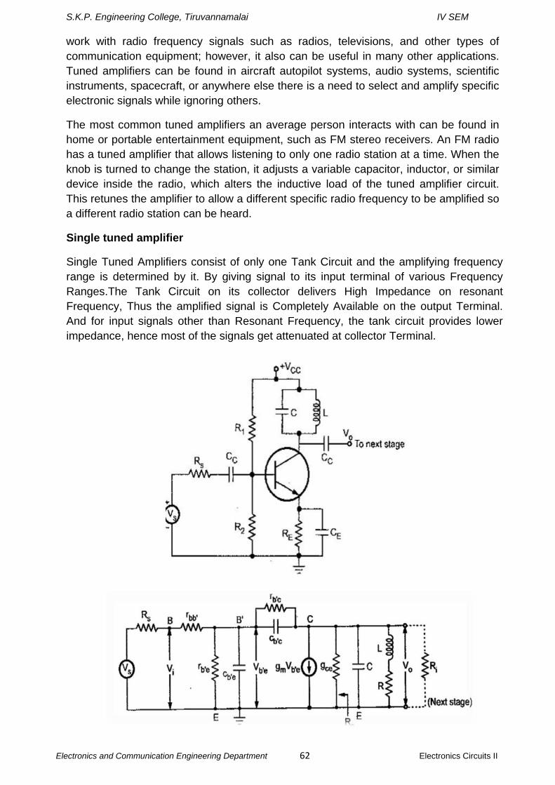
S.K.P. Engineering College, Tiruvannamalai IV SEM
Electronics and Communication Engineering Department 62 Electronics Circuits II
work with radio frequency signals such as radios, televisions, and other types of communication equipment; however, it also can be useful in many other applications. Tuned amplifiers can be found in aircraft autopilot systems, audio systems, scientific instruments, spacecraft, or anywhere else there is a need to select and amplify specific electronic signals while ignoring others.
The most common tuned amplifiers an average person interacts with can be found in home or portable entertainment equipment, such as FM stereo receivers. An FM radio has a tuned amplifier that allows listening to only one radio station at a time. When the knob is turned to change the station, it adjusts a variable capacitor, inductor, or similar device inside the radio, which alters the inductive load of the tuned amplifier circuit. This retunes the amplifier to allow a different specific radio frequency to be amplified so a different radio station can be heard.
Single tuned amplifier
Single Tuned Amplifiers consist of only one Tank Circuit and the amplifying frequency range is determined by it. By giving signal to its input terminal of various Frequency Ranges.The Tank Circuit on its collector delivers High Impedance on resonant Frequency, Thus the amplified signal is Completely Available on the output Terminal. And for input signals other than Resonant Frequency, the tank circuit provides lower impedance, hence most of the signals get attenuated at collector Terminal.
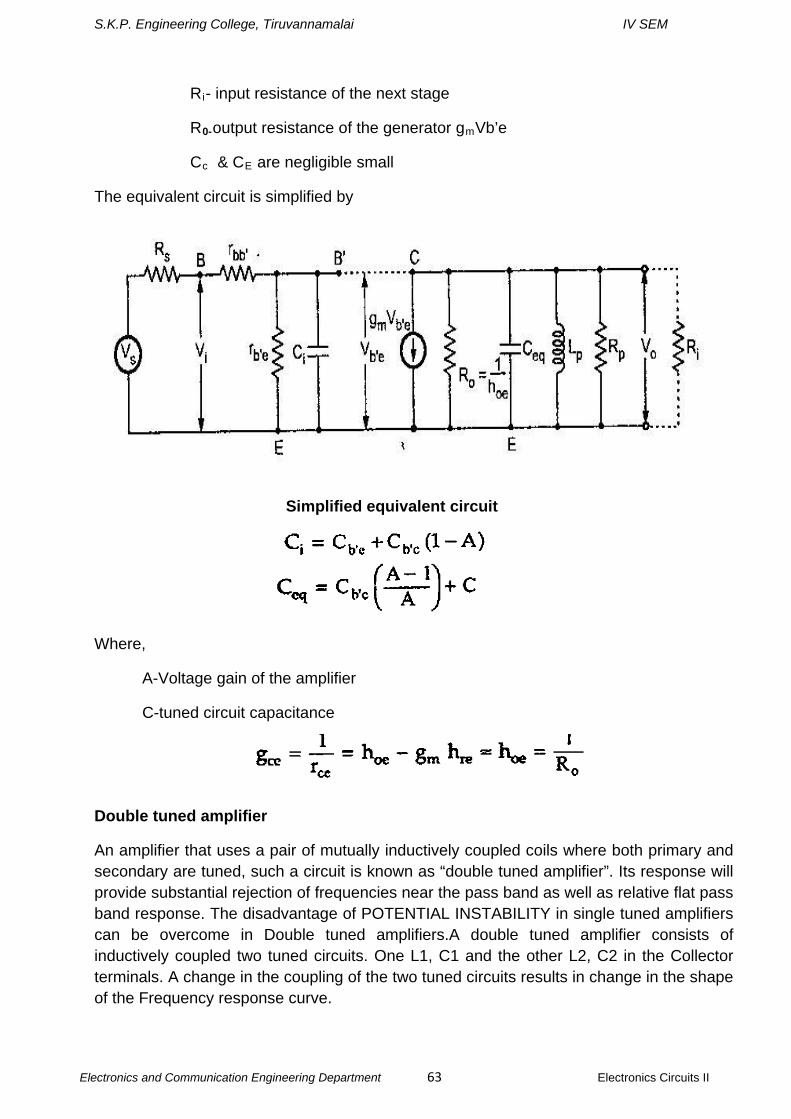
S.K.P. Engineering College, Tiruvannamalai IV SEM
Electronics and Communication Engineering Department 63 Electronics Circuits II
Ri- input resistance of the next stage
R0-output resistance of the generator gmVb’e
Cc & CE are negligible small
The equivalent circuit is simplified by
Simplified equivalent circuit
Where,
A-Voltage gain of the amplifier
C-tuned circuit capacitance
Double tuned amplifier
An amplifier that uses a pair of mutually inductively coupled coils where both primary and secondary are tuned, such a circuit is known as “double tuned amplifier”. Its response will provide substantial rejection of frequencies near the pass band as well as relative flat pass band response. The disadvantage of POTENTIAL INSTABILITY in single tuned amplifiers can be overcome in Double tuned amplifiers.A double tuned amplifier consists of inductively coupled two tuned circuits. One L1, C1 and the other L2, C2 in the Collector terminals. A change in the coupling of the two tuned circuits results in change in the shape of the Frequency response curve.

S.K.P. Engineering College, Tiruvannamalai IV SEM
Electronics and Communication Engineering Department 58 Electronics Circuits II
By proper adjustment of the coupling between the two coils of the two tuned circuits, the required results (High selectivity, high Voltage gain and required bandwidth) may be obtained.
Operation:
The high Frequency signal to be amplified is applied to the input terminal of the amplifier. The resonant Frequency of TUNED CIRCUIT connected in the Collector circuit is made equal to signal Frequency by varying the value of C1. Now the tuned circuit L1, C1 offers very high Impedance to input signal Frequency and therefore, large output is developed across it. The output from the tuned circuit L1,C1 is transferred to the second tuned circuit L2, C2 through Mutual Induction. Hence the Frequency response in Double Tuned amplifier depends on the Magnetic Coupling of L1 and L2
Equivalent circuit of double tuned amplifier:
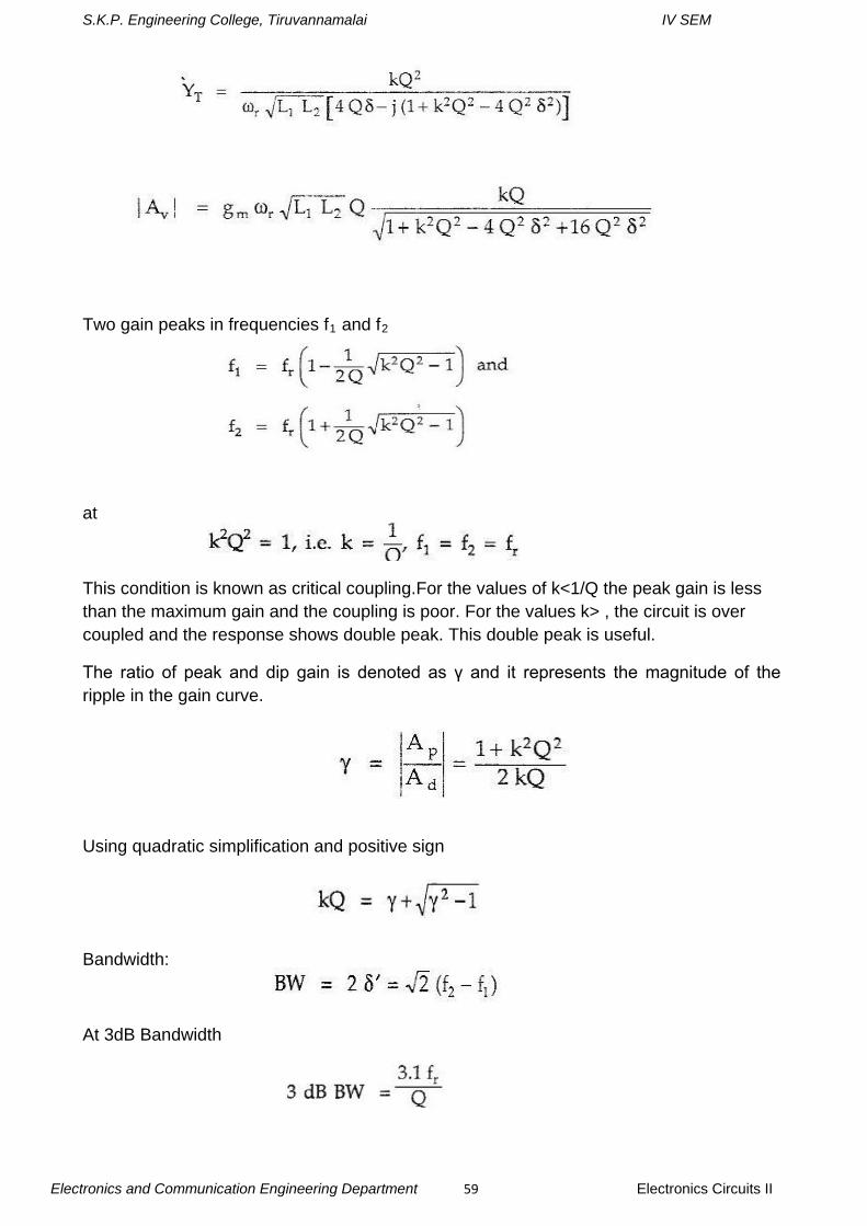
S.K.P. Engineering College, Tiruvannamalai IV SEM
Electronics and Communication Engineering Department 59 Electronics Circuits II
Two gain peaks in frequencies f1 and f2
at
This condition is known as critical coupling.For the values of k<1/Q the peak gain is less than the maximum gain and the coupling is poor. For the values k> , the circuit is over coupled and the response shows double peak. This double peak is useful.
The ratio of peak and dip gain is denoted as γ and it represents the magnitude of the ripple in the gain curve.
Using quadratic simplification and positive sign
Bandwidth:
At 3dB Bandwidth
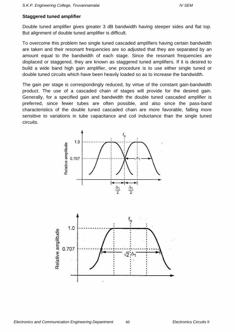
S.K.P. Engineering College, Tiruvannamalai IV SEM
Electronics and Communication Engineering Department 60 Electronics Circuits II
Staggered tuned amplifier
Double tuned amplifier gives greater 3 dB bandwidth having steeper sides and flat top. But alignment of double tuned amplifier is difficult.
To overcome this problem two single tuned cascaded amplifiers having certain bandwidth are taken and their resonant frequencies are so adjusted that they are separated by an amount equal to the bandwidth of each stage. Since the resonant frequencies are displaced or staggered, they are known as staggered tuned amplifiers. If it is desired to build a wide band high gain amplifier, one procedure is to use either single tuned or double tuned circuits which have been heavily loaded so as to increase the bandwidth.
The gain per stage is correspondingly reduced, by virtue of the constant gain-bandwidth product. The use of a cascaded chain of stages will provide for the desired gain. Generally, for a specified gain and bandwidth the double tuned cascaded amplifier is preferred, since fewer tubes are often possible, and also since the pass-band characteristics of the double tuned cascaded chain are more favorable, falling more sensitive to variations in tube capacitance and coil inductance than the single tuned circuits.
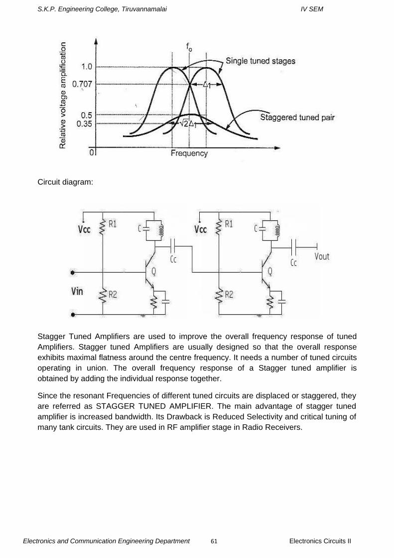
S.K.P. Engineering College, Tiruvannamalai IV SEM
Electronics and Communication Engineering Department 61 Electronics Circuits II
Circuit diagram:
Stagger Tuned Amplifiers are used to improve the overall frequency response of tuned Amplifiers. Stagger tuned Amplifiers are usually designed so that the overall response exhibits maximal flatness around the centre frequency. It needs a number of tuned circuits operating in union. The overall frequency response of a Stagger tuned amplifier is obtained by adding the individual response together.
Since the resonant Frequencies of different tuned circuits are displaced or staggered, they are referred as STAGGER TUNED AMPLIFIER. The main advantage of stagger tuned amplifier is increased bandwidth. Its Drawback is Reduced Selectivity and critical tuning of many tank circuits. They are used in RF amplifier stage in Radio Receivers.

S.K.P. Engineering College, Tiruvannamalai IV SEM
Electronics and Communication Engineering Department 62 Electronics Circuits II
Analysis
Gain of the single tuned amplifier:
Gain of the cascaded amplifier
S.K.P. Engineering College, Tiruvannamalai IV SEM
Electronics and Communication Engineering Department 63 Electronics Circuits II
UNIT IV
Wave Shaping Circuits And Multivibrators
Part-A
1. Give two applications of bistable multivibrators. [CO4-L1]
• Used to generate symmetrical square wave. This is possible by using triggering pulses of equal interval, corresponding to the frequency required.
• Used as a memory element in shift registers,counters,etc,. • Used for the performance of many digital operations like counting and storing of
digital information. • Can be used as a frequency divider
2. How does a diode act as a comparator?(NOV/DEC 2010) [CO4-L2]
A Comparator Circuit is used to identify the instant at which the arbitrary input waveformattains a particular reference level. Basically it is a clipper circuit. A simple diode comparator and its equivalent circuit is given as Consider Vin as a ramp input, increasing linearly from zero. The output will remain at VR, till input is less than , as the diode is not conducting. (ie) Vo=VR for
At t= t1, becomes equal to , after which Vo increases alongwith the input signal .
The comparator output is given to a particular device. This device will erespond when the copmparator voltage increases to some level of Vo above .
3. What is meant by clipper circuit?(APRIL/MAY 2011) [CO4-L1]
The circuits which are used to clip off the unwanted portion of the waveform, without distorting the remaining part of the waveform are called clipper circuits.
4. What is the 'tilt' applicable to RC circuits? Give an expression for tilt. (NOV/DEC 2011) [CO4-L3]
In high pass RC network, Tilt is defined as the decay in the amplitude of the output voltage waveform, when the input maintains its level constant.
Percentage of tilt is given by
Therefore
Where T- time period
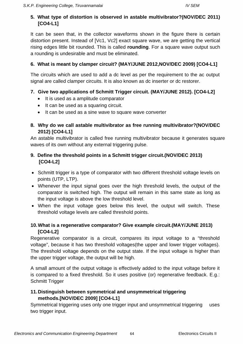
S.K.P. Engineering College, Tiruvannamalai IV SEM
Electronics and Communication Engineering Department 64 Electronics Circuits II
5. What type of distortion is observed in astable multivibrator?(NOV/DEC 2011) [CO4-L1]
It can be seen that, in the collector waveforms shown in the figure there is certain distortion present. Instead of [Vc1, Vc2] exact square wave, we are getting the vertical rising edges little bit rounded. This is called rounding. For a square wave output such a rounding is undesirable and must be eliminated.
6. What is meant by clamper circuit? (MAY/JUNE 2012,NOV/DEC 2009) [CO4-L1]
The circuits which are used to add a dc level as per the requirement to the ac output signal are called clamper circuits. It is also known as dc inserter or dc restorer.
7. Give two applications of Schmitt Trigger circuit. (MAY/JUNE 2012). [CO4-L2] • It is used as a amplitude comparator • It can be used as a squaring circuit. • It can be used as a sine wave to square wave converter
8. Why do we call astable multivibrator as free running multivibrator?(NOV/DEC
2012) [CO4-L1] An astable multivibrator is called free running multivibrator because it generates square waves of its own without any external triggering pulse.
9. Define the threshold points in a Schmitt trigger circuit.(NOV/DEC 2013) [CO4-L2]
• Schmitt trigger is a type of comparator with two different threshold voltage levels on points (UTP, LTP).
• Whenever the input signal goes over the high threshold levels, the output of the comparator is switched high. The output will remain in this same state as long as the input voltage is above the low threshold level.
• When the input voltage goes below this level, the output will switch. These threshold voltage levels are called threshold points.
10. What is a regenerative comparator? Give example circuit.(MAY/JUNE 2013)
[CO4-L2] Regenerative comparator is a circuit, compares its input voltage to a “threshold voltage”, because it has two threshold voltages(the upper and lower trigger voltages). The threshold voltage depends on the output state. If the input voltage is higher than the upper trigger voltage, the output will be high.
A small amount of the output voltage is effectively added to the input voltage before it is compared to a fixed threshold. So it uses positive (or) regenerative feedback. E.g.: Schmitt Trigger
11. Distinguish between symmetrical and unsymmetrical triggering methods.[NOV/DEC 2009] [CO4-L1]
Symmetrical triggering uses only one trigger input and unsymmetrical triggering uses two trigger input.
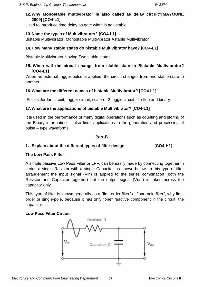
S.K.P. Engineering College, Tiruvannamalai IV SEM
Electronics and Communication Engineering Department 65 Electronics Circuits II
12. Why Monostable multivibrator is also called as delay circuit?[MAY/JUNE 2009] [CO4-L1]
Used to introduce time delay as gate width is adjustable
13. Name the types of Multivibrators? [CO4-L1] Bistable Multivibrator, Monostable Multivibrator,Astable Multivibrator
14. How many stable states do bistable Multivibrator have? [CO4-L1]
Bistable Multivibrator Having Two stable states.
15. When will the circuit change from stable state in Bistable Multivibrator? [CO4-L1] When an external trigger pulse is applied, the circuit changes from one stable state to another.
16. What are the different names of bistable Multivibrator? [CO4-L1]
Eccles Jordan circuit, trigger circuit, scale-of-2 toggle circuit, flip-flop and binary.
17. What are the applications of bistable Multivibrator? [CO4-L1]
It is used in the performance of many digital operations such as counting and storing of the Binary information. It also finds applications in the generation and processing of pulse – type waveforms
Part-B
1. Explain about the different types of filter design. [CO4-H1]
The Low Pass Filter
A simple passive Low Pass Filter or LPF, can be easily made by connecting together in series a single Resistor with a single Capacitor as shown below. In this type of filter arrangement the input signal (Vin) is applied to the series combination (both the Resistor and Capacitor together) but the output signal (Vout) is taken across the capacitor only.
This type of filter is known generally as a "first-order filter" or "one-pole filter", why first-order or single-pole, because it has only "one" reactive component in the circuit, the capacitor.
Low Pass Filter Circuit
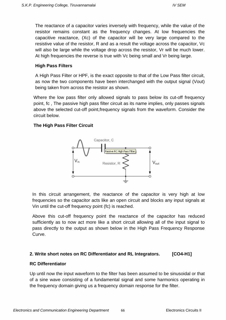
S.K.P. Engineering College, Tiruvannamalai IV SEM
Electronics and Communication Engineering Department 66 Electronics Circuits II
The reactance of a capacitor varies inversely with frequency, while the value of the resistor remains constant as the frequency changes. At low frequencies the capacitive reactance, (Xc) of the capacitor will be very large compared to the resistive value of the resistor, R and as a result the voltage across the capacitor, Vc will also be large while the voltage drop across the resistor, Vr will be much lower. At high frequencies the reverse is true with Vc being small and Vr being large.
High Pass Filters
A High Pass Filter or HPF, is the exact opposite to that of the Low Pass filter circuit, as now the two components have been interchanged with the output signal (Vout) being taken from across the resistor as shown.
Where the low pass filter only allowed signals to pass below its cut-off frequency point, fc , The passive high pass filter circuit as its name implies, only passes signals above the selected cut-off point,frequency signals from the waveform. Consider the circuit below.
The High Pass Filter Circuit
In this circuit arrangement, the reactance of the capacitor is very high at low frequencies so the capacitor acts like an open circuit and blocks any input signals at Vin until the cut-off frequency point (fc) is reached.
Above this cut-off frequency point the reactance of the capacitor has reduced sufficiently as to now act more like a short circuit allowing all of the input signal to pass directly to the output as shown below in the High Pass Frequency Response Curve.
2. Write short notes on RC Differentiator and RL Integrators. [CO4-H1]
RC Differentiator
Up until now the input waveform to the filter has been assumed to be sinusoidal or that of a sine wave consisting of a fundamental signal and some harmonics operating in the frequency domain giving us a frequency domain response for the filter.
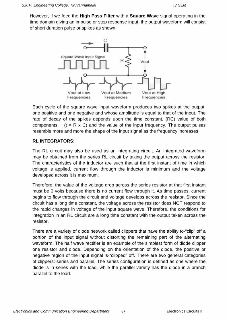
S.K.P. Engineering College, Tiruvannamalai IV SEM
Electronics and Communication Engineering Department 67 Electronics Circuits II
However, if we feed the High Pass Filter with a Square Wave signal operating in the time domain giving an impulse or step response input, the output waveform will consist of short duration pulse or spikes as shown.
Each cycle of the square wave input waveform produces two spikes at the output, one positive and one negative and whose amplitude is equal to that of the input. The rate of decay of the spikes depends upon the time constant, (RC) value of both components, (t = R x C) and the value of the input frequency. The output pulses resemble more and more the shape of the input signal as the frequency increases
RL INTEGRATORS:
The RL circuit may also be used as an integrating circuit. An integrated waveform may be obtained from the series RL circuit by taking the output across the resistor. The characteristics of the inductor are such that at the first instant of time in which voltage is applied, current flow through the inductor is minimum and the voltage developed across it is maximum.
Therefore, the value of the voltage drop across the series resistor at that first instant must be 0 volts because there is no current flow through it. As time passes, current begins to flow through the circuit and voltage develops across the resistor. Since the circuit has a long time constant, the voltage across the resistor does NOT respond to the rapid changes in voltage of the input square wave. Therefore, the conditions for integration in an RL circuit are a long time constant with the output taken across the resistor.
There are a variety of diode network called clippers that have the ability to-“clip” off a portion of the input signal without distorting the remaining part of the alternating waveform. The half wave rectifier is an example of the simplest form of diode clipper one resistor and diode. Depending on the orientation of the diode, the positive or negative region of the input signal is-“clipped” off. There are two general categories of clippers: series and parallel. The series configuration is defined as one where the diode is in series with the load, while the parallel variety has the diode in a branch parallel to the load.
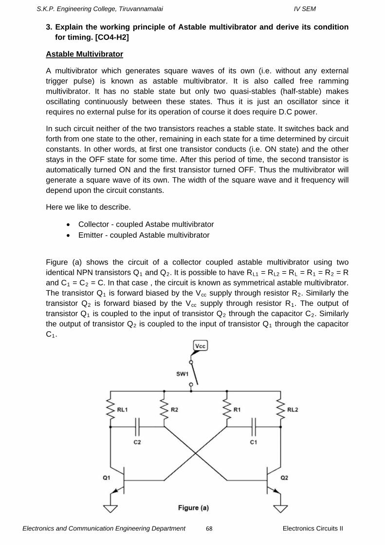
S.K.P. Engineering College, Tiruvannamalai IV SEM
Electronics and Communication Engineering Department 68 Electronics Circuits II
3. Explain the working principle of Astable multivibrator and derive its condition for timing. [CO4-H2]
Astable Multivibrator
A multivibrator which generates square waves of its own (i.e. without any external trigger pulse) is known as astable multivibrator. It is also called free ramming multivibrator. It has no stable state but only two quasi-stables (half-stable) makes oscillating continuously between these states. Thus it is just an oscillator since it requires no external pulse for its operation of course it does require D.C power.
In such circuit neither of the two transistors reaches a stable state. It switches back and forth from one state to the other, remaining in each state for a time determined by circuit constants. In other words, at first one transistor conducts (i.e. ON state) and the other stays in the OFF state for some time. After this period of time, the second transistor is automatically turned ON and the first transistor turned OFF. Thus the multivibrator will generate a square wave of its own. The width of the square wave and it frequency will depend upon the circuit constants.
Here we like to describe.
• Collector - coupled Astabe multivibrator • Emitter - coupled Astable multivibrator
Figure (a) shows the circuit of a collector coupled astable multivibrator using two identical NPN transistors Q1 and Q2. It is possible to have RL1 = RL2 = RL = R1 = R2 = R and C1 = C2 = C. In that case , the circuit is known as symmetrical astable multivibrator. The transistor Q1 is forward biased by the Vcc supply through resistor R2. Similarly the transistor Q2 is forward biased by the Vcc supply through resistor R1. The output of transistor Q1 is coupled to the input of transistor Q2 through the capacitor C2. Similarly the output of transistor Q2 is coupled to the input of transistor Q1 through the capacitor C1.
S.K.P. Engineering College, Tiruvannamalai IV SEM
Electronics and Communication Engineering Department 69 Electronics Circuits II
It consists of two common emitter amplifying stages. Each stage provides a feedback through a capacitor at the input of the other. Since the amplifying stage introduces a 180o phase shift and another 180o phase shift is introduced by a capacitor, therefore the feedback signal and the circuit works as an oscillator. In other words because of capacitive coupling none of the transistor can remain permanently out-off or saturated, instead of circuit has two quasi-stable states (ON and OFF) and it makes periodic transition between these two states.
The output of an Astable multivibrator is available at the collector terminal of the either transistors as shown in figure (a). However, the two outputs are 180o out of phase with each other. Therefore one of the outputs is said to be the complement of the other.
Let us suppose that
When Q1is ON, Q2 is OFF and
When Q2 is ON, Q1 is OFF.
When the D.C power supply is switched ON by closing S, one of the transistors will start conducting before the other (or slightly faster than the other). It is so because characteristics of no two similar transistors can be exactly alike suppose that Q1 starts conducting before Q2 does. The feedback system is such that Q1 will be very rapidly driven ton saturation and Q2 to cut-off. The circuit operation may be explained as follows.
Since Q1 is in saturation whole of VCC drops across RL1. Hence VC1 = 0 and point A is at zero or ground potential. Since Q2 is in cut-off i.e. it conducts no current, there is no drop across R L2. Hence point B is at VCC. Since A is at 0V C2 starts to charge through R2 towards VCC.
When voltage across C2 rises sufficiently (i.e. more than 0.7V), it biases Q2 in the forward direction so that it starts conducting and is soon driven to saturation.
VCC decreases and becomes almost zero when Q2 gets saturated. The potential of point B decreases from VCC to almost 0V. This potential decrease (negative swing) is applied to the base of Q1 through C1. Consequently, Q1 is pulled out of saturation and is soon driven to cut-off.
Since, now point B is at 0V, C1 starts charging through R1 towards the target voltage VCC.
When voltage of C1 increases sufficiently.Q1 becomes forward-biased and starts conducting. In this way the whole cycle is repeated.
It is observed that the circuit alternates between a state in which Q1 is ON and Q2 is OFF and the state in which Q1 is OFF and Q2 is ON. This time in each state depends on RC values. Since each transistor is driven alternately into saturation and cut-off. The voltage waveform at either collector (points A and B in figure (b)) is essentially a square waveform with peak amplitude equal to VCC.
S.K.P. Engineering College, Tiruvannamalai IV SEM
Electronics and Communication Engineering Department 70 Electronics Circuits II
Calculation of switching times and frequency of oscillations:
The frequency of oscillations can be calculated by charging and discharging capacitances and its base resistance RB.
The voltage across the capacitor can be written as
Vi= intial voltage = VB =-VCC thus the transistors enters from ON to OFF state
Vf = final voltage = VB = -VCC then the resistor enters from OFF to ON state
T1 is ON & T2 is OFF the above equation can be written as
substitute at t=T1, VB1=0 hence this equation becomes
T1=.69RB2C2
The total time period T=.694(RB1C1+RB2C2)
When RB!=RB2=R & C1=C2=C
T=1.39RC
Frequency of free running multivibrator is given by
The frequency stability of the circuit is not good as only the function of the product of RC but also depends on load resistances, supply voltages and circuit parameters. In order to stabilize the frequency, synchronizing signals are injected which terminate the unstable periods earlier than would occur naturally.
4. Explain the working principle of Bistable multivibrator and derive its condition for timing. [CO4-H2]
Bistable multivibrator
The bistable multivibrator has two absolutely stable states. It will remain in whichever state it happens to be until a trigger pulse causes it to switch to the other state. For instance, suppose at any particular instant, transistor Q1 is conducting and transistor Q 2 is at cut-off. If left to itself, the bistable multivibrator will stay in this position for ever. However, if an external pulse is applied to the circuit in such a way that Q1 is cut-off and Q2 is turned on, the circuit will stay in the new position. Another trigger pulse is then required to switch the circuit back to its original state.
In other words a multivibrator which has both the state stable is called a bistable multivibrator. It is also called flip-flop, trigger circuit or binary. The output pulse is
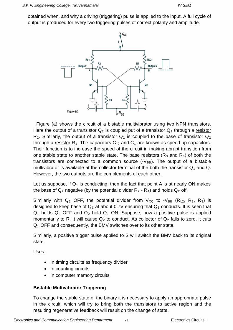
S.K.P. Engineering College, Tiruvannamalai IV SEM
Electronics and Communication Engineering Department 71 Electronics Circuits II
obtained when, and why a driving (triggering) pulse is applied to the input. A full cycle of output is produced for every two triggering pulses of correct polarity and amplitude.
Figure (a) shows the circuit of a bistable multivibrator using two NPN transistors. Here the output of a transistor Q2 is coupled put of a transistor Q1 through a resistor R2. Similarly, the output of a transistor Q1 is coupled to the base of transistor Q2 through a resistor R1. The capacitors C 2 and C1 are known as speed up capacitors. Their function is to increase the speed of the circuit in making abrupt transition from one stable state to another stable state. The base resistors (R3 and R4) of both the transistors are connected to a common source (-VBB). The output of a bistable multivibrator is available at the collector terminal of the both the transistor Q1 and Q. However, the two outputs are the complements of each other.
Let us suppose, if Q1 is conducting, then the fact that point A is at nearly ON makes the base of Q2 negative (by the potential divider R2 - R4) and holds Q2 off.
Similarly with Q2 OFF, the potential divider from VCC to -VBB (RL2, R1, R3) is designed to keep base of Q1 at about 0.7V ensuring that Q1 conducts. It is seen that Q1 holds Q2 OFF and Q2 hold Q1 ON. Suppose, now a positive pulse is applied momentarily to R. It will cause Q2 to conduct. As collector of Q2 falls to zero, it cuts Q1 OFF and consequently, the BMV switches over to its other state.
Similarly, a positive trigger pulse applied to S will switch the BMV back to its original state.
Uses:
• In timing circuits as frequency divider • In counting circuits • In computer memory circuits
Bistable Multivibrator Triggering
To change the stable state of the binary it is necessary to apply an appropriate pulse in the circuit, which will try to bring both the transistors to active region and the resulting regenerative feedback will result on the change of state.
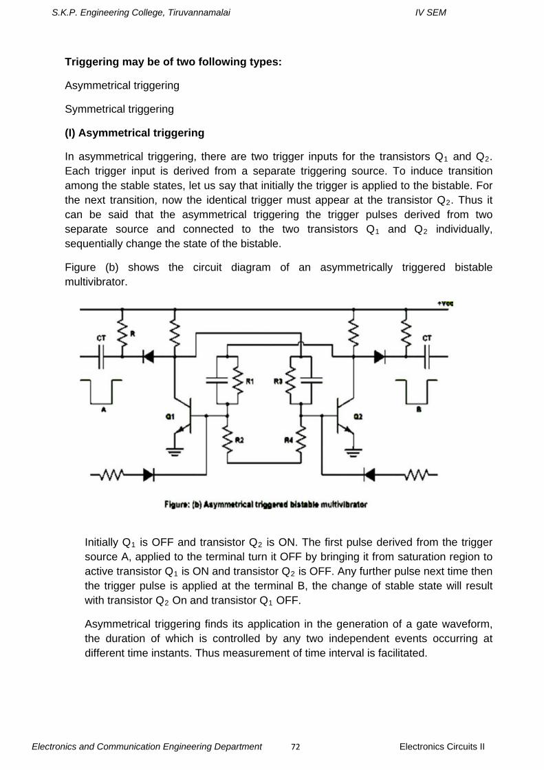
S.K.P. Engineering College, Tiruvannamalai IV SEM
Electronics and Communication Engineering Department 72 Electronics Circuits II
Triggering may be of two following types:
Asymmetrical triggering
Symmetrical triggering
(I) Asymmetrical triggering
In asymmetrical triggering, there are two trigger inputs for the transistors Q1 and Q2. Each trigger input is derived from a separate triggering source. To induce transition among the stable states, let us say that initially the trigger is applied to the bistable. For the next transition, now the identical trigger must appear at the transistor Q2. Thus it can be said that the asymmetrical triggering the trigger pulses derived from two separate source and connected to the two transistors Q1 and Q2 individually, sequentially change the state of the bistable.
Figure (b) shows the circuit diagram of an asymmetrically triggered bistable multivibrator.
Initially Q1 is OFF and transistor Q2 is ON. The first pulse derived from the trigger source A, applied to the terminal turn it OFF by bringing it from saturation region to active transistor Q1 is ON and transistor Q2 is OFF. Any further pulse next time then the trigger pulse is applied at the terminal B, the change of stable state will result with transistor Q2 On and transistor Q1 OFF.
Asymmetrical triggering finds its application in the generation of a gate waveform, the duration of which is controlled by any two independent events occurring at different time instants. Thus measurement of time interval is facilitated.
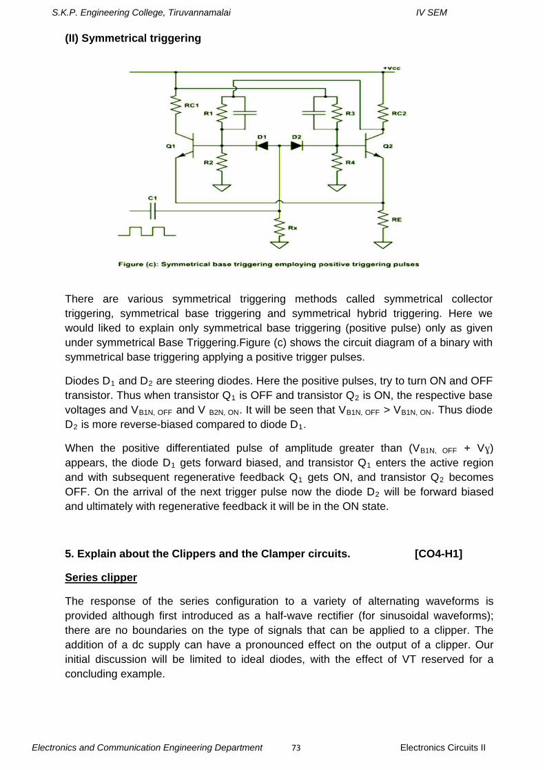
S.K.P. Engineering College, Tiruvannamalai IV SEM
Electronics and Communication Engineering Department 73 Electronics Circuits II
(II) Symmetrical triggering
There are various symmetrical triggering methods called symmetrical collector triggering, symmetrical base triggering and symmetrical hybrid triggering. Here we would liked to explain only symmetrical base triggering (positive pulse) only as given under symmetrical Base Triggering.Figure (c) shows the circuit diagram of a binary with symmetrical base triggering applying a positive trigger pulses.
Diodes D1 and D2 are steering diodes. Here the positive pulses, try to turn ON and OFF transistor. Thus when transistor Q1 is OFF and transistor Q2 is ON, the respective base voltages and VB1N, OFF and V B2N, ON. It will be seen that VB1N, OFF > VB1N, ON. Thus diode D2 is more reverse-biased compared to diode D1.
When the positive differentiated pulse of amplitude greater than (VB1N, OFF + Vɣ) appears, the diode D1 gets forward biased, and transistor Q1 enters the active region and with subsequent regenerative feedback Q1 gets ON, and transistor Q2 becomes OFF. On the arrival of the next trigger pulse now the diode D2 will be forward biased and ultimately with regenerative feedback it will be in the ON state.
5. Explain about the Clippers and the Clamper circuits. [CO4-H1]
Series clipper
The response of the series configuration to a variety of alternating waveforms is provided although first introduced as a half-wave rectifier (for sinusoidal waveforms); there are no boundaries on the type of signals that can be applied to a clipper. The addition of a dc supply can have a pronounced effect on the output of a clipper. Our initial discussion will be limited to ideal diodes, with the effect of VT reserved for a concluding example.
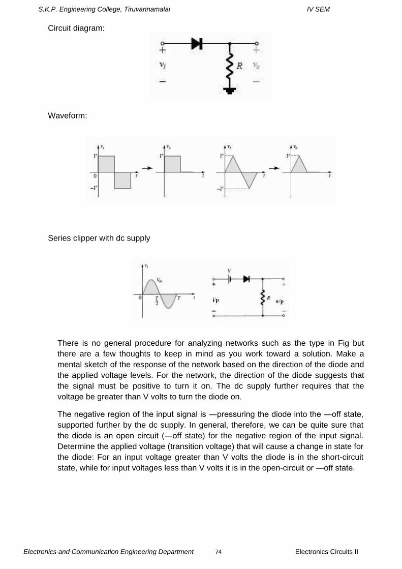
S.K.P. Engineering College, Tiruvannamalai IV SEM
Electronics and Communication Engineering Department 74 Electronics Circuits II
Circuit diagram:
Waveform:
Series clipper with dc supply
There is no general procedure for analyzing networks such as the type in Fig but there are a few thoughts to keep in mind as you work toward a solution. Make a mental sketch of the response of the network based on the direction of the diode and the applied voltage levels. For the network, the direction of the diode suggests that the signal must be positive to turn it on. The dc supply further requires that the voltage be greater than V volts to turn the diode on.
The negative region of the input signal is ―pressuring the diode into the ―off state, supported further by the dc supply. In general, therefore, we can be quite sure that the diode is an open circuit (―off state) for the negative region of the input signal. Determine the applied voltage (transition voltage) that will cause a change in state for the diode: For an input voltage greater than V volts the diode is in the short-circuit state, while for input voltages less than V volts it is in the open-circuit or ―off state.
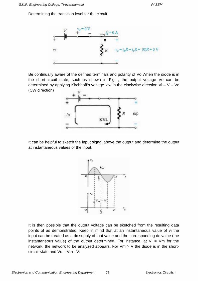
S.K.P. Engineering College, Tiruvannamalai IV SEM
Electronics and Communication Engineering Department 75 Electronics Circuits II
Determining the transition level for the circuit
Be continually aware of the defined terminals and polarity of Vo.When the diode is in the short-circuit state, such as shown in Fig. , the output voltage Vo can be determined by applying Kirchhoff‘s voltage law in the clockwise direction Vi – V – Vo (CW direction)
It can be helpful to sketch the input signal above the output and determine the output at instantaneous values of the input:
It is then possible that the output voltage can be sketched from the resulting data points of as demonstrated. Keep in mind that at an instantaneous value of vi the input can be treated as a dc supply of that value and the corresponding dc value (the instantaneous value) of the output determined. For instance, at Vi = Vm for the network, the network to be analyzed appears. For Vm > V the diode is in the short-circuit state and Vo = Vm - V.
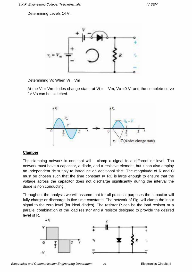
S.K.P. Engineering College, Tiruvannamalai IV SEM
Electronics and Communication Engineering Department 76 Electronics Circuits II
Determining Levels Of Vo
Determining Vo When Vi = Vm
At the Vi = Vm diodes change state; at Vi = – Vm, Vo =0 V; and the complete curve for Vo can be sketched.
Clamper
The clamping network is one that will ―clamp a signal to a different dc level. The network must have a capacitor, a diode, and a resistive element, but it can also employ an independent dc supply to introduce an additional shift. The magnitude of R and C must be chosen such that the time constant τ= RC is large enough to ensure that the voltage across the capacitor does not discharge significantly during the interval the diode is non conducting.
Throughout the analysis we will assume that for all practical purposes the capacitor will fully charge or discharge in five time constants. The network of Fig. will clamp the input signal to the zero level (for ideal diodes). The resistor R can be the load resistor or a parallel combination of the load resistor and a resistor designed to provide the desired level of R.
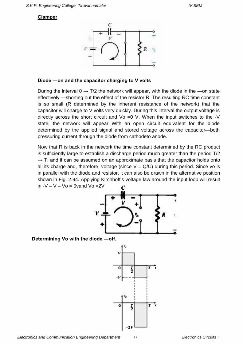
S.K.P. Engineering College, Tiruvannamalai IV SEM
Electronics and Communication Engineering Department 77 Electronics Circuits II
Clamper
Diode ―on and the capacitor charging to V volts
During the interval 0 → T/2 the network will appear, with the diode in the ―on state effectively ―shorting out the effect of the resistor R. The resulting RC time constant is so small (R determined by the inherent resistance of the network) that the capacitor will charge to V volts very quickly. During this interval the output voltage is directly across the short circuit and Vo =0 V. When the input switches to the -V state, the network will appear With an open circuit equivalent for the diode determined by the applied signal and stored voltage across the capacitor—both pressuring current through the diode from cathodeto anode.
Now that R is back in the network the time constant determined by the RC product is sufficiently large to establish a discharge period much greater than the period T/2 → T, and it can be assumed on an approximate basis that the capacitor holds onto all its charge and, therefore, voltage (since V = Q/C) during this period. Since vo is in parallel with the diode and resistor, it can also be drawn in the alternative position shown in Fig. 2.94. Applying Kirchhoff‘s voltage law around the input loop will result in -V – V – Vo = 0vand Vo =2V
Determining Vo with the diode ―off.
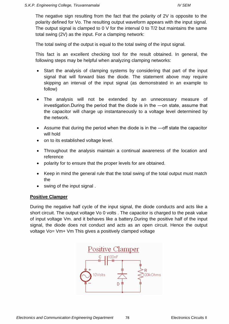
S.K.P. Engineering College, Tiruvannamalai IV SEM
Electronics and Communication Engineering Department 78 Electronics Circuits II
The negative sign resulting from the fact that the polarity of 2V is opposite to the polarity defined for Vo. The resulting output waveform appears with the input signal. The output signal is clamped to 0 V for the interval 0 to T/2 but maintains the same total swing (2V) as the input. For a clamping network:
The total swing of the output is equal to the total swing of the input signal.
This fact is an excellent checking tool for the result obtained. In general, the following steps may be helpful when analyzing clamping networks:
• Start the analysis of clamping systems by considering that part of the input signal that will forward bias the diode. The statement above may require skipping an interval of the input signal (as demonstrated in an example to follow)
• The analysis will not be extended by an unnecessary measure of investigation.During the period that the diode is in the ―on state, assume that the capacitor will charge up instantaneously to a voltage level determined by the network.
• Assume that during the period when the diode is in the ―off state the capacitor will hold
• on to its established voltage level.
• Throughout the analysis maintain a continual awareness of the location and reference
• polarity for to ensure that the proper levels for are obtained.
• Keep in mind the general rule that the total swing of the total output must match the
• swing of the input signal .
Positive Clamper
During the negative half cycle of the input signal, the diode conducts and acts like a short circuit. The output voltage Vo 0 volts . The capacitor is charged to the peak value of input voltage Vm. and it behaves like a battery.During the positive half of the input signal, the diode does not conduct and acts as an open circuit. Hence the output voltage Vo= Vm+ Vm This gives a positively clamped voltage
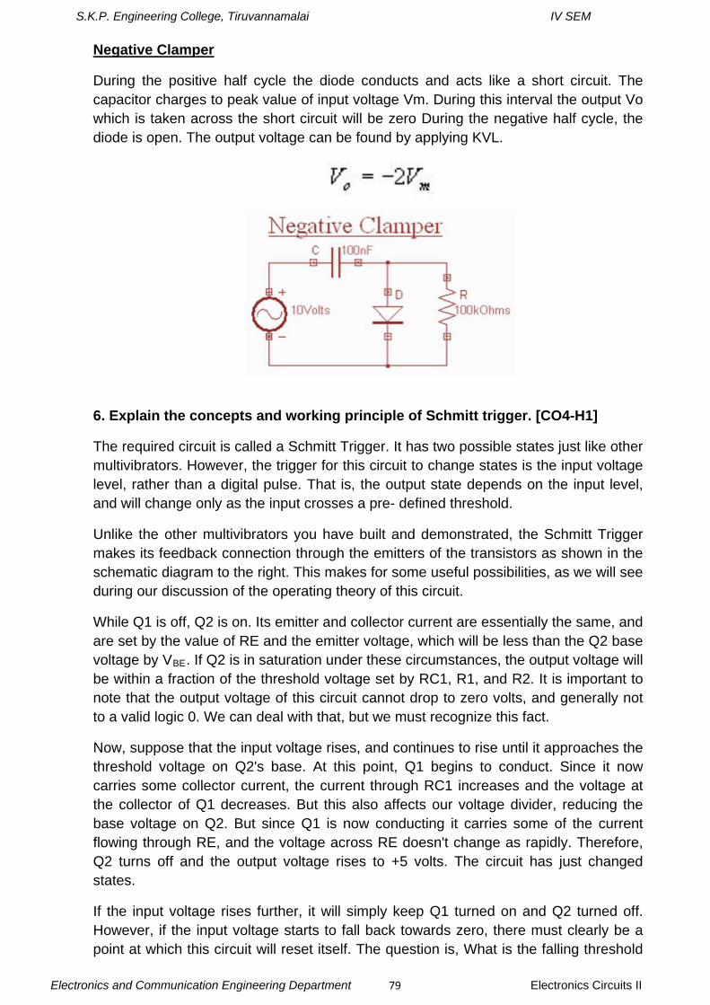
S.K.P. Engineering College, Tiruvannamalai IV SEM
Electronics and Communication Engineering Department 79 Electronics Circuits II
Negative Clamper
During the positive half cycle the diode conducts and acts like a short circuit. The capacitor charges to peak value of input voltage Vm. During this interval the output Vo which is taken across the short circuit will be zero During the negative half cycle, the diode is open. The output voltage can be found by applying KVL.
6. Explain the concepts and working principle of Schmitt trigger. [CO4-H1]
The required circuit is called a Schmitt Trigger. It has two possible states just like other multivibrators. However, the trigger for this circuit to change states is the input voltage level, rather than a digital pulse. That is, the output state depends on the input level, and will change only as the input crosses a pre- defined threshold.
Unlike the other multivibrators you have built and demonstrated, the Schmitt Trigger makes its feedback connection through the emitters of the transistors as shown in the schematic diagram to the right. This makes for some useful possibilities, as we will see during our discussion of the operating theory of this circuit.
While Q1 is off, Q2 is on. Its emitter and collector current are essentially the same, and are set by the value of RE and the emitter voltage, which will be less than the Q2 base voltage by VBE. If Q2 is in saturation under these circumstances, the output voltage will be within a fraction of the threshold voltage set by RC1, R1, and R2. It is important to note that the output voltage of this circuit cannot drop to zero volts, and generally not to a valid logic 0. We can deal with that, but we must recognize this fact.
Now, suppose that the input voltage rises, and continues to rise until it approaches the threshold voltage on Q2's base. At this point, Q1 begins to conduct. Since it now carries some collector current, the current through RC1 increases and the voltage at the collector of Q1 decreases. But this also affects our voltage divider, reducing the base voltage on Q2. But since Q1 is now conducting it carries some of the current flowing through RE, and the voltage across RE doesn't change as rapidly. Therefore, Q2 turns off and the output voltage rises to +5 volts. The circuit has just changed states.
If the input voltage rises further, it will simply keep Q1 turned on and Q2 turned off. However, if the input voltage starts to fall back towards zero, there must clearly be a point at which this circuit will reset itself. The question is, What is the falling threshold
S.K.P. Engineering College, Tiruvannamalai IV SEM
Electronics and Communication Engineering Department 80 Electronics Circuits II
voltage? It will be the voltage at which Q1's base becomes more negative than Q2's base, so that Q2 will begin conducting again. However, it isn't the same as the rising threshold voltage, since Q1 is currently affecting the behavior of the voltage divider.
We won't go through all of the derivation here, but when VIN becomes equal to Q2's base voltage, Q2's base voltage will be recognized in the Schmitt Trigger. First, the circuit will change states as VIN approaches VB2, not when the two voltages are equal. Therefore VB2 is very close to the threshold voltage, but is not precisely equal to it. For example, for the component values shown above, VB2 will be 2.54 volts when Q1 is held off, and 2.06 volts as VIN is falling towards this value.
Second, since the common emitter connection is part of the feedback system in this circuit, RE must be large enough to provide the requisite amount of feedback, without becoming so large as to starve the circuit of needed current. If RE is out of range, the circuit will not operate properly, and may not operate as anything more than a high-gain amplifier over a narrow input voltage range, instead of switching states.
The third factor is the fact that the output voltage cannot switch over logic levels, because the transistor emitters are not grounded. If a logic-level output is required, which is usually the case, we can use a circuit such as the one shown here to correct this problem. This circuit is basically two RTL inverters, except that one uses a PNP transistor. This works because when Q2 above is turned off, it will hold a PNP inverter off, but when it is on, its output will turn the PNP transistor on. The NPN transistor here is a second inverter to re-invert the signal and to restore it to active pull-down in common with all of our other logic circuits. The circuit you will construct for this experiment includes both of the circuits shown here, so that you can monitor the response of the Schmitt trigger with L0.
Schmitt Waveform Generators
Simple Waveform Generators can be constructed using basic Schmitt trigger action Inverters such as the TTL 74LS14. This method is by far the easiest way to make a basic astable waveform generator. When used to produce clock or timing signals, the astable multivibrator must produce a stable waveform that switches quickly between its "HIGH" and "LOW" states without any distortion or noise, and Schmitt inverters do just that.
We know that the output state of a Schmitt inverter is the opposite or inverse to that of its input state, (NOT Gate principles) and that it can change state at different voltage levels giving it "hysteresis". Schmitt inverters use a Schmitt Trigger action that changes state between an upper and a lower threshold level as the input voltage signal increases and decreases about the input terminal. This upper threshold level "sets" the output and the lower threshold level"resets" the output which equates to a logic "0" and a logic "1" respectively for an inverter. Consider the circuit below.
TTL Schmitt Waveform Generator
The circuit consists simply of a TTL 74LS14 Schmitt inverter logic gate with a capacitor, C connected between its input terminal and ground, (0v) with the positive feedback required for the circuit to oscillate is provided by the feedback resistor, R. So how does it work?. Assume that the charge across the capacitors plates is below the
S.K.P. Engineering College, Tiruvannamalai IV SEM
Electronics and Communication Engineering Department 81 Electronics Circuits II
Schmitt's lower threshold level of 0.8 volt (Datasheet value). This therefore makes the input to the inverter at a logic "0" level resulting in a logic "1" output level (inverter principals). One side of the resistor R is now connected to the logic "1" level (+5V) output while the other side of the resistor is connected to the capacitor, C which is at a logic "0" level (0.8v or below).
The capacitor now starts to charge up in a positive direction through the resistor at a rate determined by the RC time constant of the combination. When the charge across the capacitor reaches the 1.6 volt upper threshold level of the Schmitt trigger (Datasheet value) the output from the Schmitt inverter changes rapidly from a logic level "1" to a logic level "0" state and the current flowing through the resistor changes direction.
This change now causes the capacitor that was originally charging up through the resistor, R to begin to discharge itself back through the same resistor until the charge across the capacitors plates reaches the lower threshold level of 0.8 volts and the inverters output switches state again with the cycle repeating itself over and over again as long as the supply voltage is present.
So the capacitor, C is constantly charging and discharging itself during each cycle between the upper and lower threshold levels of the Schmitt inverter producing a logic level "1" or a logic level "0" at the inverters output. However, the output square wave signal is not symmetrical producing a duty cycle of about 33% or 1/3 as the mark-to-space ratio between "HIGH" and "LOW" is 1:2 respectively due to the input gate characteristics of the TTL inverter.
The value of the feedback resistor, R MUST also be kept low to below 1kΩ for the circuit to oscillate correctly, 220R to 470R is good, and by varying the value of the capacitor, C to vary the frequency. Also at high frequency levels the output waveform changes shape from a square shaped waveform to a trapezoidal shaped waveform as the input characteristics of the TTL gate are affected by the rapid charging and discharging of the capacitor.
With a resistor value between: 100R to 1kΩ, and a capacitor value of between: 1nF to 1000uF. This would give a frequency range of between 1Hzto 1MHz, (high frequencies produce waveform distortion).
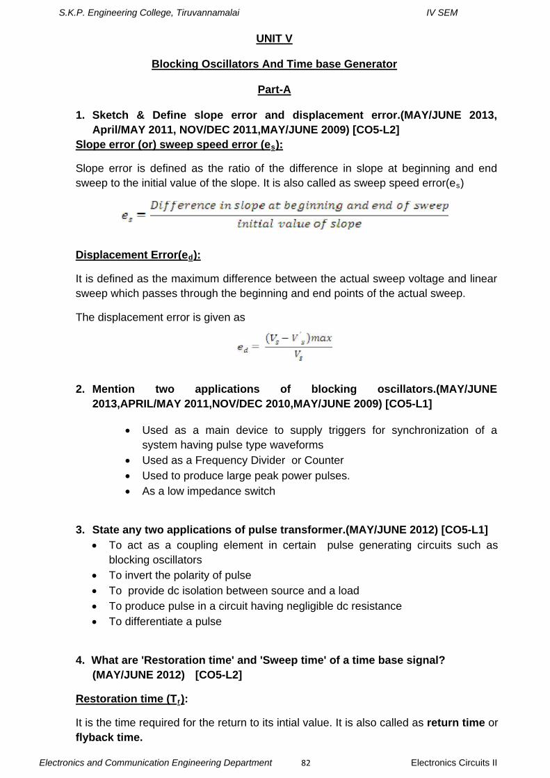
S.K.P. Engineering College, Tiruvannamalai IV SEM
Electronics and Communication Engineering Department 82 Electronics Circuits II
UNIT V
Blocking Oscillators And Time base Generator
Part-A
1. Sketch & Define slope error and displacement error.(MAY/JUNE 2013, April/MAY 2011, NOV/DEC 2011,MAY/JUNE 2009) [CO5-L2]
Slope error (or) sweep speed error (es):
Slope error is defined as the ratio of the difference in slope at beginning and end sweep to the initial value of the slope. It is also called as sweep speed error(es)
Displacement Error(ed):
It is defined as the maximum difference between the actual sweep voltage and linear sweep which passes through the beginning and end points of the actual sweep.
The displacement error is given as
2. Mention two applications of blocking oscillators.(MAY/JUNE 2013,APRIL/MAY 2011,NOV/DEC 2010,MAY/JUNE 2009) [CO5-L1]
• Used as a main device to supply triggers for synchronization of a system having pulse type waveforms
• Used as a Frequency Divider or Counter • Used to produce large peak power pulses. • As a low impedance switch
3. State any two applications of pulse transformer.(MAY/JUNE 2012) [CO5-L1] • To act as a coupling element in certain pulse generating circuits such as
blocking oscillators • To invert the polarity of pulse • To provide dc isolation between source and a load • To produce pulse in a circuit having negligible dc resistance • To differentiate a pulse
4. What are 'Restoration time' and 'Sweep time' of a time base signal? (MAY/JUNE 2012) [CO5-L2]
Restoration time (Tr):
It is the time required for the return to its intial value. It is also called as return time or flyback time.

S.K.P. Engineering College, Tiruvannamalai IV SEM
Electronics and Communication Engineering Department 83 Electronics Circuits II
Sweep time(Ts):
It is the period during which voltage increases linearly
5. Define Blocking Oscillator? [CO5-L1]
A special type of wave generator which is used to produce a single narrow pulse or train of pulses
6. What are the two important elements of Blocking Oscillator? [CO5-L1]
Transistor and pulse transformer
7. What are the applications of blocking Oscillator? [CO5-L1]
It is used in frequency dividers, counter circuits and for switching the other circuits.
8. Give the formula for transformation ratio [CO5-L1]
Transformation ratio n= Ns/Np
Ns= Secondary Turns
Np= Primary turns
9. Define rise time [CO5-L1]
It is defined by the time required by the pulse to rise from 10% of its amplitude to 90% of its amplitude.
10. Define overshoot. [CO5-L1]
It is the amount by which the output exceeds its amplitude during first attempt. Define flat top response. The position of the response between the trailing edge and the leading edge.
11. Define droop or a tilt. [CO5-L1]
The displacement of the pulse amplitude during its flat response is called droop or a tilt.
12. What are the applications of pulse transformer? [CO5-L1]
• To invert the polarity of the pulse
• To differentiate pulse
13. When the core does saturate? [CO5-L1]
When L->o as B-> Bm, the core saturates
14. What is the other name of astable Blocking Oscillator [CO5-L1]
Free running blocking Oscillator
S.K.P. Engineering College, Tiruvannamalai IV SEM
Electronics and Communication Engineering Department 84 Electronics Circuits II
15. What are the two types of astable Blocking Oscillator? [CO5-L1]
• Diode controlled Astable Blocking Oscillator.
• Re controlled Astable Blocking Oscillator
16. Define Sweeptime in sawtooth generator [CO5-L1]
The period during which voltage increases linearly is called sweep time
17. What is the other name of sawtooth generator? [CO5-L1]
Ramp generator
18. Define Displacement error in the sawtooth generator? [CO5-L2]
It is defined as the maximum differenece between the actual sweep voltage and linear sweep which passes through the beginning and end points of the actual sweep.
19. What is constant current charging? [CO5-L1]
A capacitor is charged with a constant current source.
20. Define Sweep time in saw tooth generator. [CO5-L1]
The period during which voltage increases linearly is called sweep time.
21. Define Displacement error in the saw tooth generator? [CO5-L2]
It is defined as the maximum differences between the actual sweep voltage and linear sweep which passes through the beginning and end points of the actual sweep.
22. What is constant current charging? [CO5-L1]
A capacitor is charged with a constant current source.
23. What is the miller circuit? [CO5-L1]
Integrator is used to convert a step waveform into ramp waveform.
24. Define Duty cycle. [CO5-L1]
The duty cycle is defined as the ratio of the ON time tp to the time period T. Mathematically it is given by, D= tp/T
25. How high duty cycle is obtained? [CO5-L1]
• Using temperature compensated zener diode
• Using Ge diode in series with tertiary winding across the supply voltage.
26. What do you mean by voltage time base generators? [CO5-L1]
Circuits used to generate a linear variation of voltage with time are called Voltage time-base generators.

S.K.P. Engineering College, Tiruvannamalai IV SEM
Electronics and Communication Engineering Department 85 Electronics Circuits II
27. List the applications of time base generators.(NOV/DEC 2013) [CO5-L2] • Used in CRO(Cathode Ray Oscilloscope) • Used in Television and radar displays • Used in precise time measurements • Used in time modulation
28. What are tha advantages of core saturation method of frequency control in a Blocking oscillator?(NOV/DEC 2012) [CO5-L3] The pulse duration depends on the supply voltage and characteristics of the core and not on the transistor parameters (hfe).
The pulse width is given by
Part-B
1. Explain the different type of Saw tooth Wave. [CO5-H1]
A sawtooth wave can be generated by using an RC network. Possibly the simplest sawtooth generator. Assume that at T0, S1 is placed in position P. At the instant the switch closes, the applied voltage (Ea) appears at R. C begins to charge to E a through R. If S1 remains closed long enough, C will fully charge to Ea. You should remember from NEETS, Module 2, Alternating Current and Transformers, that a capacitor takes 5 time constants (5TC)to fully charge.
As the capacitor charges to the applied voltage, the rate of charge follows an exponential curve. If a linear voltage is desired, the full charge time of the capacitor cannot be used because the exponential curve becomes nonlinear during the first time constant.
Unijunction Saw tooth Generator.
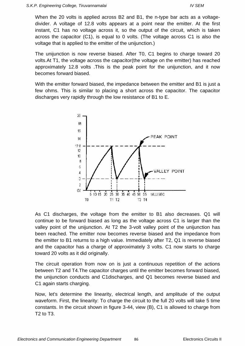
S.K.P. Engineering College, Tiruvannamalai IV SEM
Electronics and Communication Engineering Department 86 Electronics Circuits II
When the 20 volts is applied across B2 and B1, the n-type bar acts as a voltage- divider. A voltage of 12.8 volts appears at a point near the emitter. At the first instant, C1 has no voltage across it, so the output of the circuit, which is taken across the capacitor (C1), is equal to 0 volts. (The voltage across C1 is also the voltage that is applied to the emitter of the unijunction.)
The unijunction is now reverse biased. After T0, C1 begins to charge toward 20 volts.At T1, the voltage across the capacitor(the voltage on the emitter) has reached approximately 12.8 volts .This is the peak point for the unijunction, and it now becomes forward biased.
With the emitter forward biased, the impedance between the emitter and B1 is just a few ohms. This is similar to placing a short across the capacitor. The capacitor discharges very rapidly through the low resistance of B1 to E.
As C1 discharges, the voltage from the emitter to B1 also decreases. Q1 will continue to be forward biased as long as the voltage across C1 is larger than the valley point of the unijunction. At T2 the 3-volt valley point of the unijunction has been reached. The emitter now becomes reverse biased and the impedance from the emitter to B1 returns to a high value. Immediately after T2, Q1 is reverse biased and the capacitor has a charge of approximately 3 volts. C1 now starts to charge toward 20 volts as it did originally.
The circuit operation from now on is just a continuous repetition of the actions between T2 and T4.The capacitor charges until the emitter becomes forward biased, the unijunction conducts and C1discharges, and Q1 becomes reverse biased and C1 again starts charging.
Now, let's determine the linearity, electrical length, and amplitude of the output waveform. First, the linearity: To charge the circuit to the full 20 volts will take 5 time constants. In the circuit shown in figure 3-44, view (B), C1 is allowed to charge from T2 to T3.
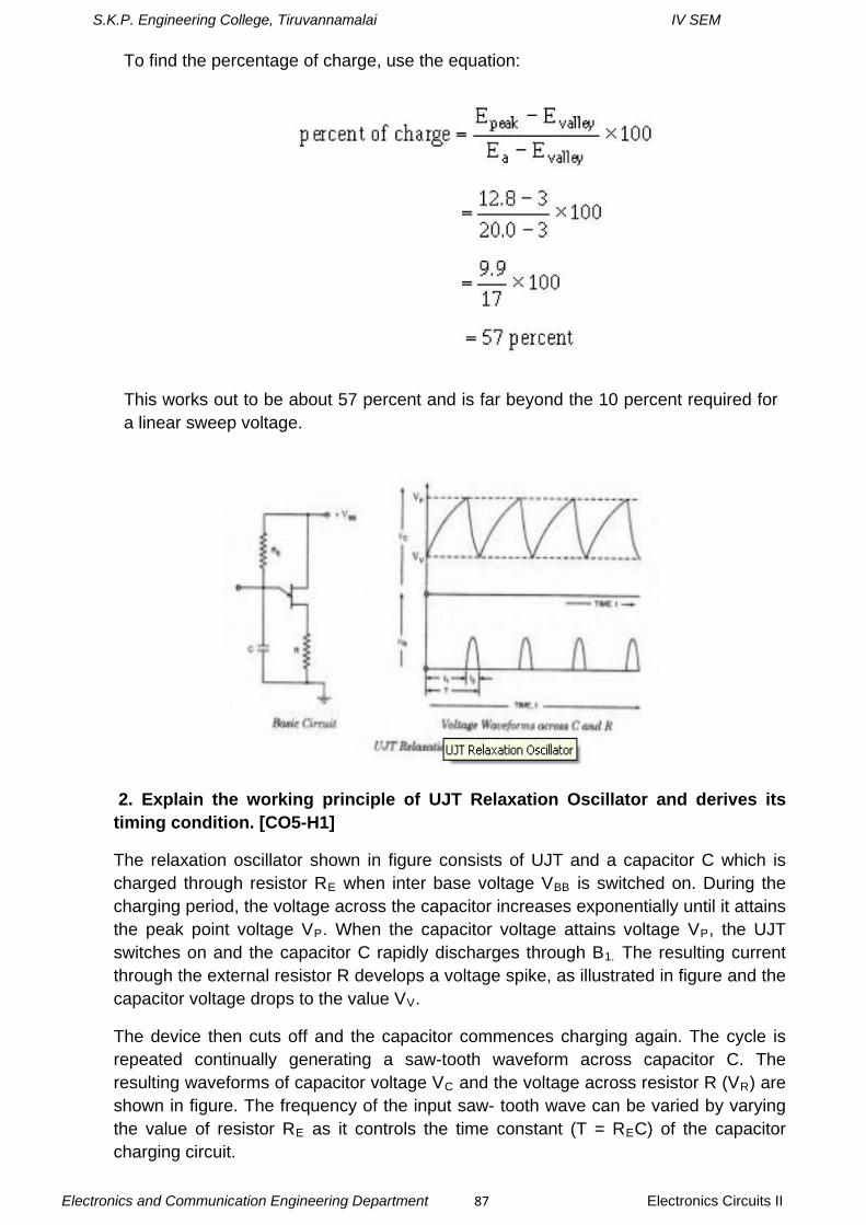
S.K.P. Engineering College, Tiruvannamalai IV SEM
Electronics and Communication Engineering Department 87 Electronics Circuits II
To find the percentage of charge, use the equation:
This works out to be about 57 percent and is far beyond the 10 percent required for a linear sweep voltage.
2. Explain the working principle of UJT Relaxation Oscillator and derives its timing condition. [CO5-H1]
The relaxation oscillator shown in figure consists of UJT and a capacitor C which is charged through resistor RE when inter base voltage VBB is switched on. During the charging period, the voltage across the capacitor increases exponentially until it attains the peak point voltage VP. When the capacitor voltage attains voltage VP, the UJT switches on and the capacitor C rapidly discharges through B1. The resulting current through the external resistor R develops a voltage spike, as illustrated in figure and the capacitor voltage drops to the value VV.
The device then cuts off and the capacitor commences charging again. The cycle is repeated continually generating a saw-tooth waveform across capacitor C. The resulting waveforms of capacitor voltage VC and the voltage across resistor R (VR) are shown in figure. The frequency of the input saw- tooth wave can be varied by varying the value of resistor RE as it controls the time constant (T = REC) of the capacitor charging circuit.
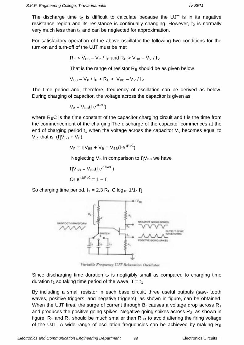
S.K.P. Engineering College, Tiruvannamalai IV SEM
Electronics and Communication Engineering Department 88 Electronics Circuits II
The discharge time t2 is difficult to calculate because the UJT is in its negative resistance region and its resistance is continually changing. However, t2 is normally very much less than t1 and can be neglected for approximation.
For satisfactory operation of the above oscillator the following two conditions for the turn-on and turn-off of the UJT must be met
RE < VBB – VP / IP and RE > VBB – VV / IV
That is the range of resistor RE should be as given below
VBB – VP / IP > RE > VBB – VV / IV
The time period and, therefore, frequency of oscillation can be derived as below. During charging of capacitor, the voltage across the capacitor is given as
Vc = VBB(l-e-/ReC)
where REC is the time constant of the capacitor charging circuit and t is the time from the commencement of the charging.The discharge of the capacitor commences at the end of charging period t1 when the voltage across the capacitor Vc becomes equal to VP, that is, (ȠVBB + VB)
VP = ȠVBB + VB = VBB(l-e-/ReC)
Neglecting VB in comparison to ȠVBB we have
ȠVBB = VBB(l-e-1/ReC)
Or e-t1/ReC = 1 – Ƞ
So charging time period, t1 = 2.3 RE C log10 1/1- Ƞ
Since discharging time duration t2 is negligibly small as compared to charging time duration t1 so taking time period of the wave, T = t1
By including a small resistor in each base circuit, three useful outputs (saw- tooth waves, positive triggers, and negative triggers), as shown in figure, can be obtained. When the UJT fires, the surge of current through Bt causes a voltage drop across R1 and produces the positive going spikes. Negative-going spikes across R2, as shown in figure. R1 and R2 should be much smaller than RBB to avoid altering the firing voltage of the UJT. A wide range of oscillation frequencies can be achieved by making RE
S.K.P. Engineering College, Tiruvannamalai IV SEM
Electronics and Communication Engineering Department 89 Electronics Circuits II
adjustable and including a switch to select different values of capacitance, as illustrated. As already mentioned in previous blog post there is upper and lower limits to the signal source resistance RE for the satisfactory operation of the UJT.
3. Write short notes on Pulse Transformer. [CO5-H1]
A pulse transformer is a transformer that is optimised for transmitting rectangular electrical pulses (that is, pulses with fast rise and fall times and a relatively constant amplitude). Small versions called signal types are used in digital logic and telecommunications circuits, often for matching logic drivers to transmission lines. Medium-sized power versions are used in power-control circuits such as camera flash controllers. Larger power versions are used in the electrical power distribution industry to interface low-voltage control circuitry to the high-voltage gates of power semiconductors. Special high voltage pulse transformers are also used to generate high power pulses for radar, particle accelerators, or other high energy pulsed power applications.
To minimize distortion of the pulse shape, a pulse transformer needs to have low values of leakage inductance and distributed capacitance, and a highopen-circuit inductance. In power-type pulse transformers, a low coupling capacitance (between the primary and secondary) is important to protect the circuitry on the primary side from high-powered transients created by the load.
For the same reason, high insulation resistance and high breakdown voltage are required. A good transient response is necessary to maintain the rectangular pulse shape at the secondary, because a pulse with slow edges would create switching losses in the power semiconductors.
The product of the peak pulse voltage and the duration of the pulse (or more accurately, the voltage-time integral) is often used to characterize pulse transformers. Generally speaking, the larger this product, the larger and more expensive the transformer Pulse transformers by definition have a duty cycle of less than 0.5, whatever energy stored in the coil during the pulse must be "dumped" out before the pulse is fired again.
4. Describe about the blocking oscillator and explain its application. [CO4-H1]
Blocking Oscillator
The BLOCKING OSCILLATOR is a special type of wave generator used to produce a narrow pulse, or trigger. Blocking oscillators have many uses, most of which are concerned with the timing of some other circuit. They can be used as frequency dividers or counter circuits and for switching other circuits on and off at specific times.
In a blocking oscillator the pulse width (pw), pulse repetition time (prt), and pulse repetition rate (prr) are all controlled by the size of certain capacitors and resistors and by the operating characteristics of the transformer. The transformer primary determines the duration and shape of the output. Because of their importance in the circuit, transformer action and series RL circuits will be discussed briefly. You may
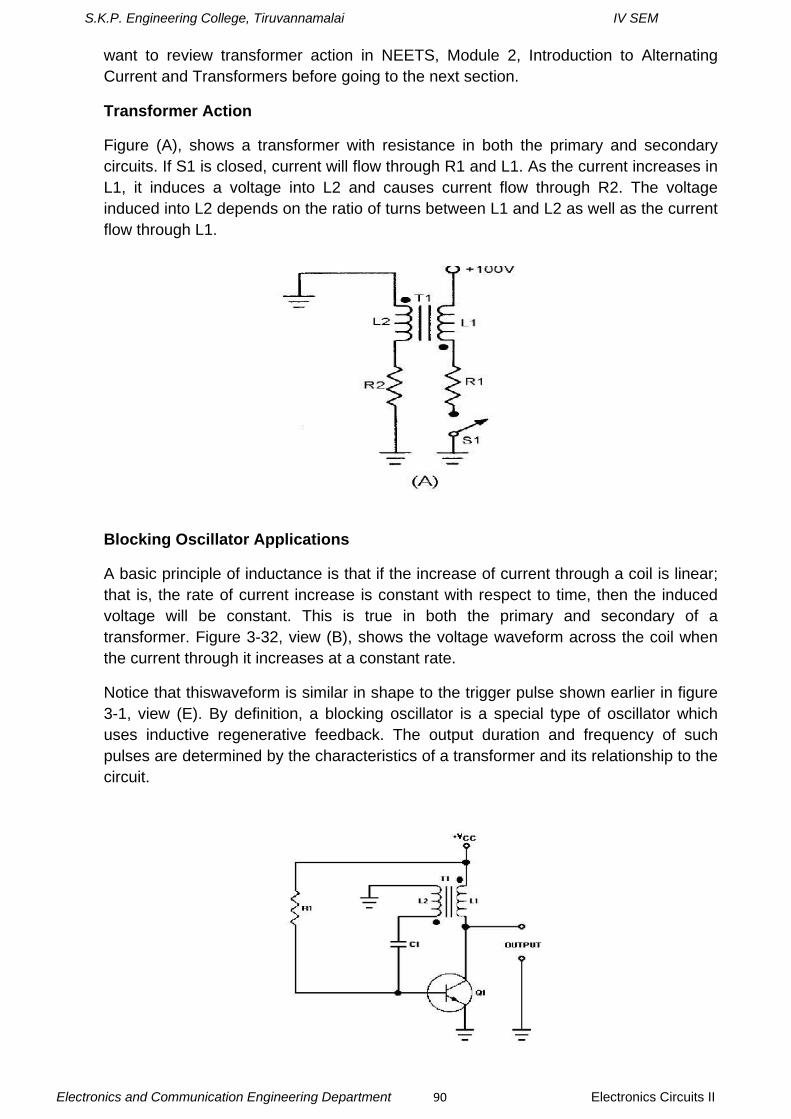
S.K.P. Engineering College, Tiruvannamalai IV SEM
Electronics and Communication Engineering Department 90 Electronics Circuits II
want to review transformer action in NEETS, Module 2, Introduction to Alternating Current and Transformers before going to the next section.
Transformer Action
Figure (A), shows a transformer with resistance in both the primary and secondary circuits. If S1 is closed, current will flow through R1 and L1. As the current increases in L1, it induces a voltage into L2 and causes current flow through R2. The voltage induced into L2 depends on the ratio of turns between L1 and L2 as well as the current flow through L1.
Blocking Oscillator Applications
A basic principle of inductance is that if the increase of current through a coil is linear; that is, the rate of current increase is constant with respect to time, then the induced voltage will be constant. This is true in both the primary and secondary of a transformer. Figure 3-32, view (B), shows the voltage waveform across the coil when the current through it increases at a constant rate.
Notice that thiswaveform is similar in shape to the trigger pulse shown earlier in figure 3-1, view (E). By definition, a blocking oscillator is a special type of oscillator which uses inductive regenerative feedback. The output duration and frequency of such pulses are determined by the characteristics of a transformer and its relationship to the circuit.

S.K.P. Engineering College, Tiruvannamalai IV SEM
Electronics and Communication Engineering Department 91 Electronics Circuits II
When power is applied to the circuit, R1 provides forward bias and transistor Q1 conducts. Current flow through Q1 and the primary of T1 induces a voltage in L2. The phasing dots on the transformer indicate a 180-degree phase shift. As the bottom side of L1 is going negative, the bottom side of L2 is going positive. The positive voltage of L2 is coupled to the base of the transistor through C1, and Q1conducts more.
This provides more collector current and more current through L1. This action is regenerative feedback. Very rapidly, sufficient voltage is applied to saturate the base of Q1. Once the base becomes saturated, it loses control over collector current. The circuit now can be compared to a small resistor (Q1) in series with a relatively large inductor (L1), or a series RL circuit.
5. State any two methods of achieving sweep linearity of a time-base waveform.(NOV/DEC2012)
• Exponential charging • Constant current charging • Miller circuit • Bootstrap circuit.
Blocking oscillator idealized waveforms
The operation of the circuit to this point has generated a very steep leading edge for the output pulse.Figure 3-34 shows the idealized collector and base waveforms. Once the base of Q1 becomes saturated, the current increase in L1 is determined by the
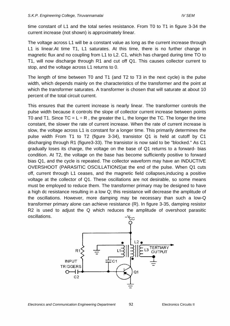
S.K.P. Engineering College, Tiruvannamalai IV SEM
Electronics and Communication Engineering Department 92 Electronics Circuits II
time constant of L1 and the total series resistance. From T0 to T1 in figure 3-34 the current increase (not shown) is approximately linear.
The voltage across L1 will be a constant value as long as the current increase through L1 is linear.At time T1, L1 saturates. At this time, there is no further change in magnetic flux and no coupling from L1 to L2. C1, which has charged during time TO to T1, will now discharge through R1 and cut off Q1. This causes collector current to stop, and the voltage across L1 returns to 0.
The length of time between T0 and T1 (and T2 to T3 in the next cycle) is the pulse width, which depends mainly on the characteristics of the transformer and the point at which the transformer saturates. A transformer is chosen that will saturate at about 10 percent of the total circuit current.
This ensures that the current increase is nearly linear. The transformer controls the pulse width because it controls the slope of collector current increase between points T0 and T1. Since TC = L ÷ R , the greater the L, the longer the TC. The longer the time constant, the slower the rate of current increase. When the rate of current increase is slow, the voltage across L1 is constant for a longer time. This primarily determines the pulse width From T1 to T2 (figure 3-34), transistor Q1 is held at cutoff by C1 discharging through R1 (figure3-33). The transistor is now said to be "blocked." As C1 gradually loses its charge, the voltage on the base of Q1 returns to a forward- bias condition. At T2, the voltage on the base has become sufficiently positive to forward bias Q1, and the cycle is repeated. The collector waveform may have an INDUCTIVE OVERSHOOT (PARASITIC OSCILLATIONS)at the end of the pulse. When Q1 cuts off, current through L1 ceases, and the magnetic field collapses,inducing a positive voltage at the collector of Q1. These oscillations are not desirable, so some means must be employed to reduce them. The transformer primary may be designed to have a high dc resistance resulting in a low Q; this resistance will decrease the amplitude of the oscillations. However, more damping may be necessary than such a low-Q transformer primary alone can achieve resistance (R). In figure 3-35, damping resistor R2 is used to adjust the Q which reduces the amplitude of overshoot parasitic oscillations.
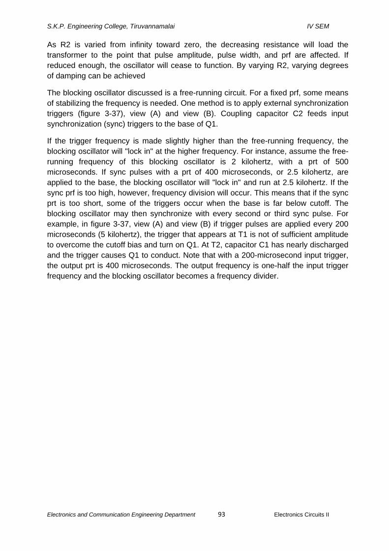
S.K.P. Engineering College, Tiruvannamalai IV SEM
Electronics and Communication Engineering Department 93 Electronics Circuits II
As R2 is varied from infinity toward zero, the decreasing resistance will load the transformer to the point that pulse amplitude, pulse width, and prf are affected. If reduced enough, the oscillator will cease to function. By varying R2, varying degrees of damping can be achieved
The blocking oscillator discussed is a free-running circuit. For a fixed prf, some means of stabilizing the frequency is needed. One method is to apply external synchronization triggers (figure 3-37), view (A) and view (B). Coupling capacitor C2 feeds input synchronization (sync) triggers to the base of Q1.
If the trigger frequency is made slightly higher than the free-running frequency, the blocking oscillator will "lock in" at the higher frequency. For instance, assume the free-running frequency of this blocking oscillator is 2 kilohertz, with a prt of 500 microseconds. If sync pulses with a prt of 400 microseconds, or 2.5 kilohertz, are applied to the base, the blocking oscillator will "lock in" and run at 2.5 kilohertz. If the sync prf is too high, however, frequency division will occur. This means that if the sync prt is too short, some of the triggers occur when the base is far below cutoff. The blocking oscillator may then synchronize with every second or third sync pulse. For example, in figure 3-37, view (A) and view (B) if trigger pulses are applied every 200 microseconds (5 kilohertz), the trigger that appears at T1 is not of sufficient amplitude to overcome the cutoff bias and turn on Q1. At T2, capacitor C1 has nearly discharged and the trigger causes Q1 to conduct. Note that with a 200-microsecond input trigger, the output prt is 400 microseconds. The output frequency is one-half the input trigger frequency and the blocking oscillator becomes a frequency divider.