simulation of ultra-small electronic devices: quantum ... · simulation of ultra-small electronic...
TRANSCRIPT
� � � � � � � � � � � � � � � � � �� � � � � � � � � � � � � � � � � � � � � � � � � � � � � � �� � � � � � � � � � � � � � � � � � � � � �
Simulation of Ultra-Small Electr onic De vices:Quantum Corrections to Classical Models
Br yan Bieg el
NAS Device Modeling W orkshop, A ugust 7-8, 1997
Projects
• Wigner function and transfer-matrix modeling of macroscopicquantum devices in 3-D
• Quantum corrections to classical drift-diffusion and hydrodynamicmodels in 3-D
� � � � � � � � � � � � � � � � � �� � � � � � � � � � � � � � � � � � � � � � � � � � � � � � �� � � � � � � � � � � � � � � � � � � � � �
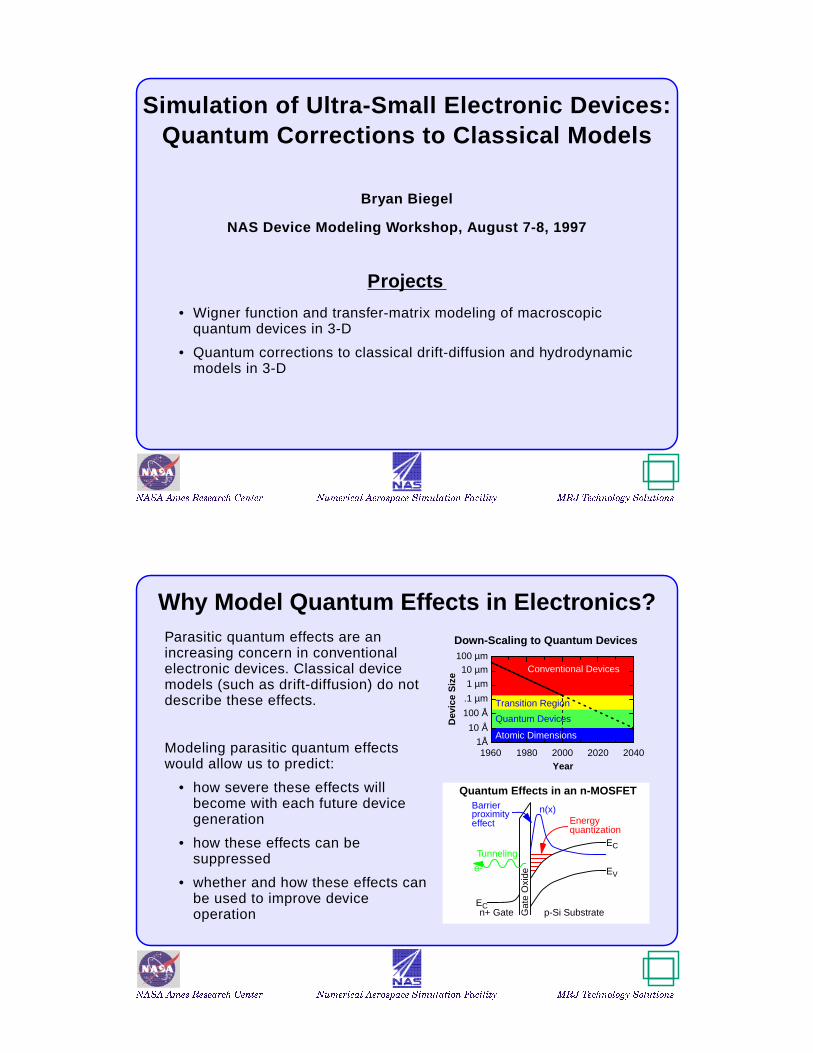
Why Model Quantum Eff ects in Electr onics?Parasitic quantum effects are anincreasing concern in conventionalelectronic devices. Classical devicemodels (such as drift-diffusion) do notdescribe these effects.
Modeling parasitic quantum effectswould allow us to predict:
• how severe these effects willbecome with each future devicegeneration
• how these effects can besuppressed
• whether and how these effects canbe used to improve deviceoperation
1960 1980 2000 2020 2040Year
1Å
10 Å
100 Å
.1 µm
1 µm
10 µm100 µm
Conventional Devices
Dev
ice
Siz
e
Transition Region
Quantum Devices
Atomic Dimensions
Down-Scaling to Quantum De vices
n+ Gate Gat
e O
xide
EC
EV
EC
n(x)
Tunneling
Energy
Barrier
quantization
e-
p-Si Substrate
proximityeffect
Quantum Eff ects in an n-MOSFET
� � � � � � � � � � � � � � � � � �� � � � � � � � � � � � � � � � � � � � � � � � � � � � � � �� � � � � � � � � � � � � � � � � � � � � �
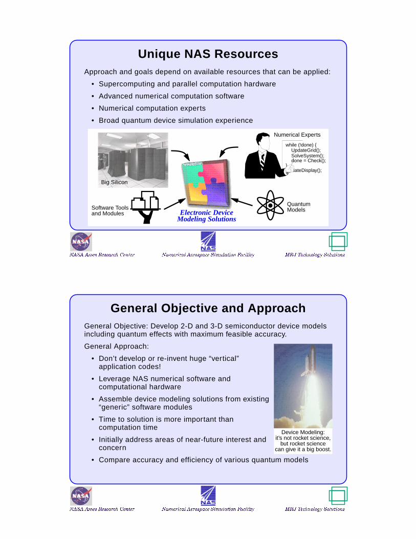
Unique NAS Resour cesApproach and goals depend on available resources that can be applied:
• Supercomputing and parallel computation hardware
• Advanced numerical computation software
• Numerical computation experts
• Broad quantum device simulation experience
UpdateDisplay();
while (!done) {
Electronic Device
SolveSystem();
Modeling Solutions
Software Toolsand Modules
Big Silicon
QuantumModels
Numerical Experts
UpdateGrid();
done = Check();}
� � � � � � � � � � � � � � � � � �� � � � � � � � � � � � � � � � � � � � � � � � � � � � � � �� � � � � � � � � � � � � � � � � � � � � �
General Objective and Appr oachGeneral Objective: Develop 2-D and 3-D semiconductor device modelsincluding quantum effects with maximum feasible accuracy.
General Approach:
• Don’t develop or re-invent huge “vertical”application codes!
• Leverage NAS numerical software andcomputational hardware
• Assemble device modeling solutions from existing“generic” software modules
• Time to solution is more important thancomputation time
• Initially address areas of near-future interest andconcern
• Compare accuracy and efficiency of various quantum models
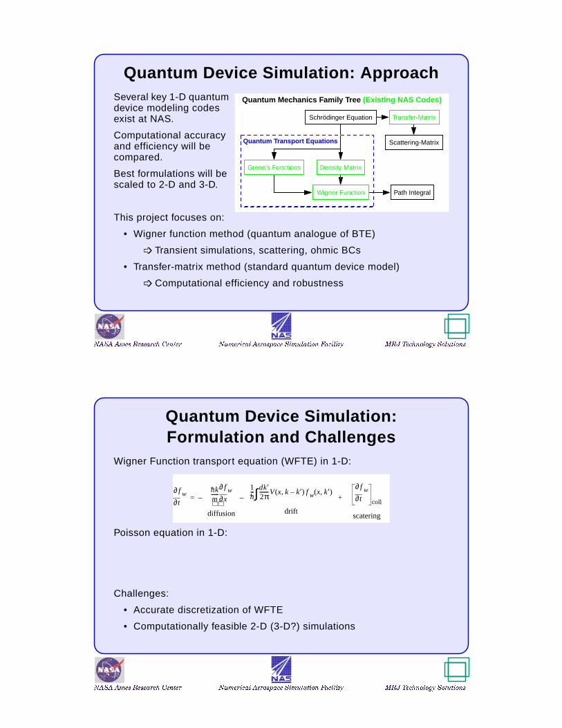
Device Modeling:it’s not rocket science,
but rocket sciencecan give it a big boost.

� � � � � � � � � � � � � � � � � �� � � � � � � � � � � � � � � � � � � � � � � � � � � � � � �� � � � � � � � � � � � � � � � � � � � � �
AbstractInterest and concern is increasing about quantum effects in electronic devices as down-scaling is expected to continue through the next two decades. Technology leaders need toknow how significantly parasitic quantum effects will degrade electronic device operation witheach future device generation, how long these effects can be suppressed and by whatmeans, and how quantum effects might be used to actually improve device operation. Thereare two main reasons why simulation tools can not yet provide this information: 1) convertingnew electronic device models including quantum effects into functioning simulation softwareis very time-consuming, and 2) the required computational resources for accurate simulationsof commercially important electronic devices are immense. Both of these difficulties areaddressed by this project, the goal of which is the rapid and accurate investigation ofquantum effects in near-future electronic devices.
This project addresses the first issue by utilizing advanced NAS software modules andemerging third-party numerical computation tools to rapidly implement and investigate newelectronic device models including quantum effects. The second issue is also addressed bythe availability of highly capable parallel computation systems at NAS. Specific projectsplanned for this work include the investigation of quantum effects in 1-D structures using anexisting quantum device simulation tool, and the rapid implementation of quantum correctionsin 1-D, 2-D and 3-D to the classical drift-diffusion, hydrodynamic, and BTE models of electrontransport. The test device for most of this work will be the MOSFET, in which quantum effectsare the highest concern, due to its dominance in electronics and to the wide range ofquantum effects which are increasingly significant in this device.
� � � � � � � � � � � � � � � � � �� � � � � � � � � � � � � � � � � � � � � � � � � � � � � � �� � � � � � � � � � � � � � � � � � � � � �
Quantum De vice Sim ulation: Motiv ationInvestigate electronic systems where quantum effects are dominant:
• Gain experience in how quantum effects manifest themselves, forapplication to quantum corrections studies
• Knowledge of quantum models for derivation of quantum corrections
• “Map out” entire spectrum between classical and quantum realms
• Analyze capabilities of proposed/demonstrated quantum devices
• Eventually, electronics will go quantum or go nowhere - quantumsimulation allows us to probe this domain before this ultimatum, andbefore experimental evidence is available (or at least feasible).
Progression of Electr onic De vices fr om Classical to Quantum
Device ➩MOSFET
BJT
MODFETHET
QWLD
RTDRTT
QUITSQUID
QuantumDot, SET
QuantumComputer
ClassicalEffects
Dominant Dominant Significant ParasiticParasitic ,Negligib le
Computation-killer
QuantumEffects
Parasitic Useful Significant Dominant Dominant Exclusiv e
� � � � � � � � � � � � � � � � � �� � � � � � � � � � � � � � � � � � � � � � � � � � � � � � �� � � � � � � � � � � � � � � � � � � � � �
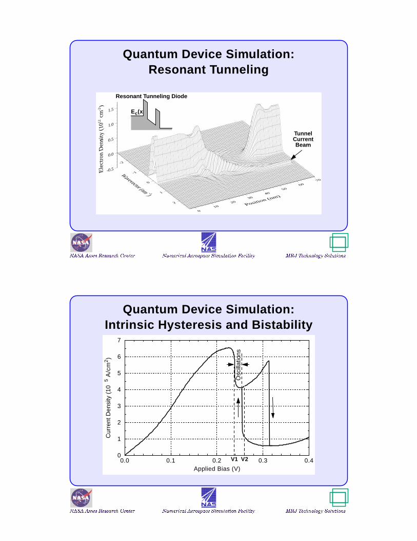
Quantum De vice Sim ulation: Appr oachSeveral key 1-D quantumdevice modeling codesexist at NAS.
Computational accuracyand efficiency will becompared.
Best formulations will bescaled to 2-D and 3-D.
This project focuses on:
• Wigner function method (quantum analogue of BTE)
➩ Transient simulations, scattering, ohmic BCs
• Transfer-matrix method (standard quantum device model)
➩ Computational efficiency and robustness
Schrödinger Equation Transfer-Matrix
Scattering-MatrixQuantum T ranspor t Equations
Green’s Functions Density Matrix
Wigner Function Path Integral
Quantum Mec hanics F amil y Tree (Existing NAS Codes)
� � � � � � � � � � � � � � � � � �� � � � � � � � � � � � � � � � � � � � � � � � � � � � � � �� � � � � � � � � � � � � � � � � � � � � �
Quantum De vice Sim ulation:Form ulation and Challeng es
Wigner Function transport equation (WFTE) in 1-D:
Poisson equation in 1-D:
Challenges:
• Accurate discretization of WFTE
• Computationally feasible 2-D (3-D?) simulations
t∂∂ f w
h_
km------
x∂∂ f w
diffusion
–1h_---
dk ′2π-------V x k k ′–,( ) f w x k ′,( )∫
drift
t∂∂ f w
coll
scatering
+–=
î î î
x∂∂ ε x( )
x∂∂
u x( ) qρ x( ) q2
C x( ) c x( )–[ ]= = u x( ), U x( ) δU x( )–=
� � � � � � � � � � � � � � � � � �� � � � � � � � � � � � � � � � � � � � � � � � � � � � � � �� � � � � � � � � � � � � � � � � � � � � �
Quantum De vice Sim ulation:Resonant T unneling
010
2030
4050
6070
Position (nm)
2
1
0
-1
-2
Wavevector (nm -1)
-0.5
0.0
0.5
1.0
1.5
Ele
ctro
n D
ensi
ty (
10
�
12 c
m-2
)Resonant T unneling Diode
Ec(x)
TunnelCurrentBeam
� � � � � � � � � � � � � � � � � �� � � � � � � � � � � � � � � � � � � � � � � � � � � � � � �� � � � � � � � � � � � � � � � � � � � � �
Quantum De vice Sim ulation:Intrinsic Hysteresis and Bistability
0.0 0.1 0.2 0.3 0.4Applied Bias (V)
0
1
2
3
4
5
6
7
Cur
rent
Den
sity
(10
5 A
/cm
2)
Osc
illat
ions
V2V1
� � � � � � � � � � � � � � � � � �� � � � � � � � � � � � � � � � � � � � � � � � � � � � � � �� � � � � � � � � � � � � � � � � � � � � �
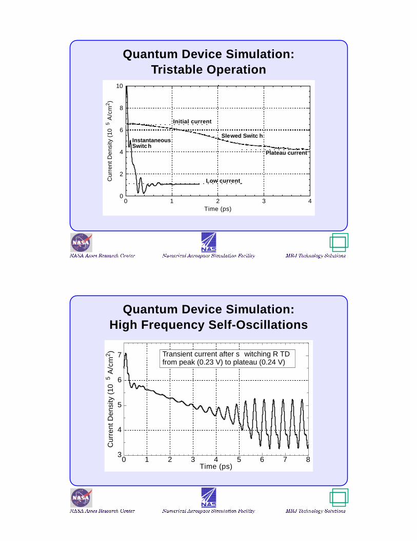
Quantum De vice Sim ulation:Tristab le Operation
0 1 2 3 4Time (ps)
0
2
4
6
8
10
Cur
rent
Den
sity
(10
5 A
/cm
2)
Low current
Initial current
Plateau current
InstantaneousSwitc h
Slewed Switc h
� � � � � � � � � � � � � � � � � �� � � � � � � � � � � � � � � � � � � � � � � � � � � � � � �� � � � � � � � � � � � � � � � � � � � � �
Quantum De vice Sim ulation:High Frequenc y Self-Oscillations
0 1 2 3 4 5 6 7 8Time (ps)
3
4
5
6
7
Cur
rent
Den
sity
(10
5 A
/cm
2) Transient current after s witching R TD
from peak (0.23 V) to plateau (0.24 V)
� � � � � � � � � � � � � � � � � �� � � � � � � � � � � � � � � � � � � � � � � � � � � � � � �� � � � � � � � � � � � � � � � � � � � � �
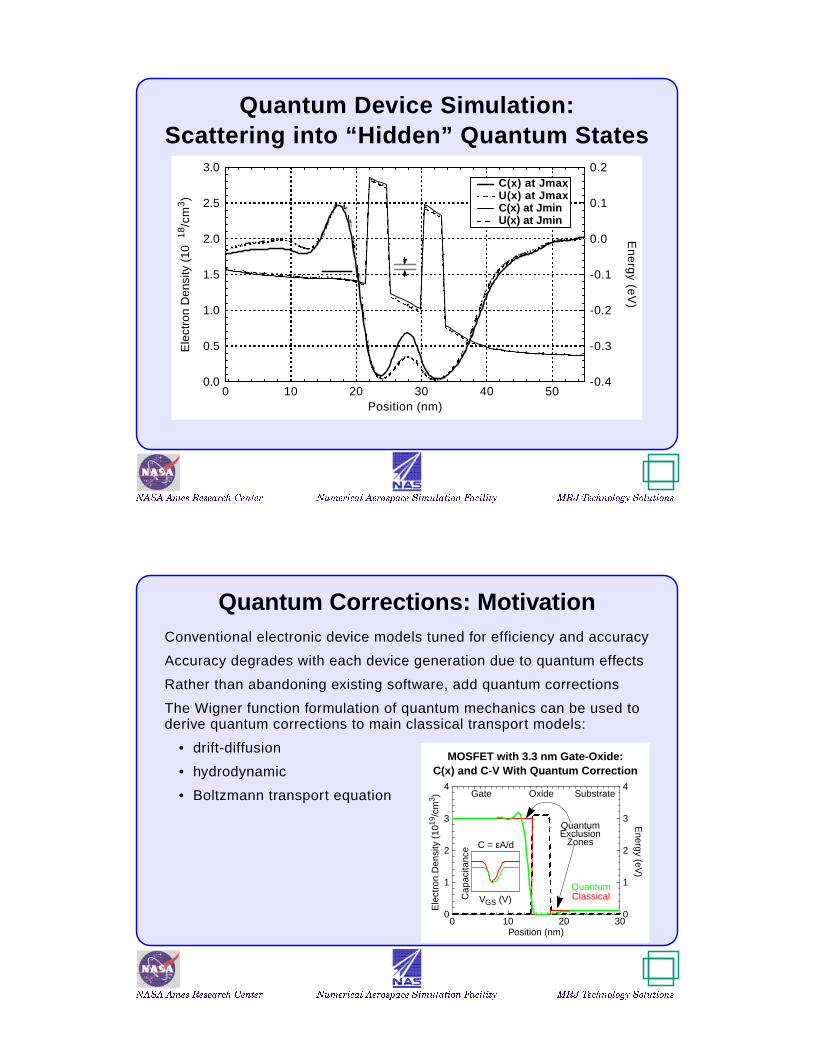
Quantum De vice Sim ulation:Scattering into “Hid den” Quantum States
0 10 20 30 40 50Position (nm)
0.0
0.5
1.0
1.5
2.0
2.5
3.0
Ele
ctro
n D
ensi
ty (
101
8/c
m3)
C(x) at JmaxU(x) at JmaxC(x) at JminU(x) at Jmin
-0.4
-0.3
-0.2
-0.1
0.0
0.1
0.2E
ne
rgy (e
V)
� � � � � � � � � � � � � � � � � �� � � � � � � � � � � � � � � � � � � � � � � � � � � � � � �� � � � � � � � � � � � � � � � � � � � � �
Quantum Corrections: Motiv ationConventional electronic device models tuned for efficiency and accuracy
Accuracy degrades with each device generation due to quantum effects
Rather than abandoning existing software, add quantum corrections
The Wigner function formulation of quantum mechanics can be used toderive quantum corrections to main classical transport models:
• drift-diffusion
• hydrodynamic
• Boltzmann transport equation
MOSFET with 3.3 nm Gate-Oxide:C(x) and C-V With Quantum Correction
0 10 20 30Position (nm)
0
1
2
3
4
Ele
ctro
n D
ensi
ty (
1019
/cm
3 )
0
1
2
3
4
Energy (eV
)
Gate SubstrateOxide
QuantumExclusion
ZonesC = εA/d
VGS (V)Cap
acita
nce
QuantumClassical

� � � � � � � � � � � � � � � � � �� � � � � � � � � � � � � � � � � � � � � � � � � � � � � � �� � � � � � � � � � � � � � � � � � � � � �
Quantum Corrections: Drift-Diffusion ModelDensity-Gradient Model [Ancona, PRB 39(13), 9536]:
Quantum potentials:
Implementation Challenges:
• 1-D, 2-D, 3-D capability
• Grid-independent
• Extensible (e.g., position-, temperature-, density-dependent )
∇ ε∇ ψ( )⋅ q– p n– ND+
N A-
–+( )=
t∂∂n ∇ Dn n∇ nµn ψ ψqn+( )∇–[ ]⋅=
t∂∂p ∇ Dp p∇ pµp ψ ψqp+( )∇+[ ]⋅=
ψqn 2bnn∇ 2
n--------------
≡ ψqp 2– bpp∇ 2
p--------------
≡ bn p,h_2
12mn p,* q-----------------------≡, ,
bn p,
� � � � � � � � � � � � � � � � � �� � � � � � � � � � � � � � � � � � � � � � � � � � � � � � �� � � � � � � � � � � � � � � � � � � � � �
Quantum Corrections: Appr oachUnproductive time between defining physical model and analyzingsimulation results should be minimized. This time includes:
• Deriving numerical model
• Incorporating third-party code toreduce programming task
• Programming (writing thesoftware)
• Debugging the software
• Waiting for simulation results
Conclusion: Simulation softwareshould be built at the highestpossible level.
In theory, all components ofunproductive time except simulationcan be virtually eliminated.
Distribution of Effort inSimulation Software Development
Low-Level High-Level
Physics
Program
Debug
Numerics
Simulation
Construction
Modules
Construction
% o
f Effo
rt
100
Unproductive Productive
Analysis

� � � � � � � � � � � � � � � � � �� � � � � � � � � � � � � � � � � � � � � � � � � � � � � � �� � � � � � � � � � � � � � � � � � � � � �
Quantum Corrections: Software T oolsMany classical models and quantum corrections need to be rapidlyinvestigated
Ideal electronic device simulator:
• Model descr iption as system of PDEs
• Simple specification of de vice str ucture ,mater ial par ameters , device tests
• Automatic selection of n umer ical algor ithms
• High-quality g raphical output
Software tools under consider ation/e valuation:
• PROPHET (Gener al PDE solv er)
• PDE Solv er under de velopment in NAS Process Modeling Group
• NAS Parallel equation solv er codes (linear and non-linear systems)
• NAS 3-D P oisson Solv er, 3-D Dynamic g ridding codes
• Various computational fluid dynamics (CFD) codes
∇ 2ψ q– ρ ε⁄=
Device Simulator
Ideal Device Sim ulator
C-VI-V
V(x,y)