simulation of quantum parametric amplifiers
TRANSCRIPT

Simulation of Quantum Parametric Amplifiers
by
Keith Krause
A thesis submitted to the Graduate Faculty ofAuburn University
in partial fulfillment of therequirements for the Degree of
Master of Science
Auburn, AlabamaAugust 7, 2021
Keywords: Parametric amplifiers, Simulations, Josephson junctions, Quantum phase-slips
Copyright 2021 by Keith Krause
Approved by
Michael C. Hamilton, Chair, James B. Davis Professor of Electrical and ComputerEngineering
Mark Lee Adams, Associate Professor of Electrical and Computer EngineeringMasoud Mahjouri Samani, Assistant Professor of Electrical and Computer Engineering
Peng Li, Assistant Professor of Electrical and Computer Engineering

Abstract
Parametric amplifiers couple a nonlinear element to an external environment, resulting in
frequency mixing of a pump tone and a smaller signal tone. The pump’s energy is coupled into
the signal tone and an additional idler tone. Josephson parametric amplifiers have achieved near
quantum limited performance, and they are well-suited for qubit readout in quantum comput-
ing applications. They use the Josephson junction’s nonlinear inductance to create a nonlinear
resonator. While there has been much research done on these Josephson parametric ampli-
fiers, there has not yet been a parametric amplifier which uses quantum phase-slip junctions.
Quantum phase-slip junctions are the voltage-based counterpart to the current-based Joseph-
son junction. This thesis uses simulations to design and analyze quantum phase-slip junction
based parametric amplifiers. The simulation data shown in this thesis demonstrates frequency
mixing and gain of the signal tone, two important characteristics of a working parametric am-
plifier. This thesis also shows simulation experiments on various aspects of the quantum phase-
slip based parametric amplifier, including the critical voltage and bias voltage of the quantum
phase-slip junctions.
ii

Acknowledgments
I would like to express my thanks for my advisor and committee chair, Dr. Michael C.
Hamilton, whose guidance, input, and advice was incredibly beneficial in my work as a gradu-
ate student and the completion of this thesis.
I am indebted to Dr. Uday S. Goteti, who was remarkably kind and helpful to me during
my time as both an undergraduate and graduate researcher, and created the quantum phase-slip
junction model used extensively in this thesis.
I am thankful for every single one of my peers in the Auburn Nanosystems Group. They
have been very supportive and I would not have been able to graduate without them.
I would like to thank my committee members Dr. Mark Lee Adams, Dr. Masoud Mahjouri
Samani, and Dr. Peng Li for their time and help.
Finally, I would like to extend my deepest thanks to my parents and family, who have
carried me through difficult times in graduate school and in life.
iii

Table of Contents
Abstract . . . . . . . . . . . . . . . . . . . . . . . . . . . . . . . . . . . . . . . . . . . ii
Acknowledgments . . . . . . . . . . . . . . . . . . . . . . . . . . . . . . . . . . . . . . iii
List of Abbreviations . . . . . . . . . . . . . . . . . . . . . . . . . . . . . . . . . . . . x
1 Introduction . . . . . . . . . . . . . . . . . . . . . . . . . . . . . . . . . . . . . . . 1
1.1 Parametric amplifiers in qubit state measurement . . . . . . . . . . . . . . . . 2
1.2 Josephson junctions . . . . . . . . . . . . . . . . . . . . . . . . . . . . . . . . 3
1.2.1 Nonlinear inductance . . . . . . . . . . . . . . . . . . . . . . . . . . . 3
1.3 Quantum phase-slip junctions . . . . . . . . . . . . . . . . . . . . . . . . . . . 5
1.4 Nondegenerate amplification . . . . . . . . . . . . . . . . . . . . . . . . . . . 5
1.5 Degenerate amplification . . . . . . . . . . . . . . . . . . . . . . . . . . . . . 7
1.6 Gain vs. bandwith in a parametric amplifier . . . . . . . . . . . . . . . . . . . 7
1.7 Quantum Langevin equation . . . . . . . . . . . . . . . . . . . . . . . . . . . 8
1.8 Simple parametric amplifier . . . . . . . . . . . . . . . . . . . . . . . . . . . . 10
1.9 Flux-driven parametric amplifier using a DC SQUID . . . . . . . . . . . . . . 12
1.10 Josephson parametric converter . . . . . . . . . . . . . . . . . . . . . . . . . . 14
1.11 Traveling-wave parametric amplifier . . . . . . . . . . . . . . . . . . . . . . . 15
1.11.1 Four-wave mixing . . . . . . . . . . . . . . . . . . . . . . . . . . . . . 16
1.11.2 Three-wave mixing . . . . . . . . . . . . . . . . . . . . . . . . . . . . 17
1.12 SQUID-based parametric amplifier . . . . . . . . . . . . . . . . . . . . . . . . 18
iv
2 Traveling-wave parametric amplifiers . . . . . . . . . . . . . . . . . . . . . . . . . . 21
2.1 Current JJ-based traveling-wave parametric amplifiers . . . . . . . . . . . . . . 21
2.2 Directionality . . . . . . . . . . . . . . . . . . . . . . . . . . . . . . . . . . . 22
2.3 JJ-based traveling-wave parametric amplifier . . . . . . . . . . . . . . . . . . . 23
2.3.1 Simulation circuit design . . . . . . . . . . . . . . . . . . . . . . . . . 23
2.4 Simulation results . . . . . . . . . . . . . . . . . . . . . . . . . . . . . . . . . 24
2.4.1 Circuit length . . . . . . . . . . . . . . . . . . . . . . . . . . . . . . . 24
2.4.2 Bias current . . . . . . . . . . . . . . . . . . . . . . . . . . . . . . . . 26
2.4.3 Critical current . . . . . . . . . . . . . . . . . . . . . . . . . . . . . . 27
2.5 QPSJ-based traveling-wave parametric amplifier . . . . . . . . . . . . . . . . . 28
2.5.1 Simulation circuit design . . . . . . . . . . . . . . . . . . . . . . . . . 28
2.6 Simulation results . . . . . . . . . . . . . . . . . . . . . . . . . . . . . . . . . 29
2.6.1 Circuit length . . . . . . . . . . . . . . . . . . . . . . . . . . . . . . . 29
2.6.2 Bias voltage . . . . . . . . . . . . . . . . . . . . . . . . . . . . . . . . 31
2.6.3 Critical voltage . . . . . . . . . . . . . . . . . . . . . . . . . . . . . . 32
3 Lumped-element parametric amplifier . . . . . . . . . . . . . . . . . . . . . . . . . 34
3.1 Phase dependency . . . . . . . . . . . . . . . . . . . . . . . . . . . . . . . . . 34
3.2 JJ-based flux-driven parametric amplifiers . . . . . . . . . . . . . . . . . . . . 36
3.2.1 Simulation circuit design . . . . . . . . . . . . . . . . . . . . . . . . . 37
3.2.2 Separation of incident and reflected waves . . . . . . . . . . . . . . . . 37
3.2.3 Simulation results . . . . . . . . . . . . . . . . . . . . . . . . . . . . . 38
3.3 QPSJ-based lumped-element parametric amplifier . . . . . . . . . . . . . . . . 39
3.3.1 Simulation circuit design . . . . . . . . . . . . . . . . . . . . . . . . . 40
3.3.2 Simulation results . . . . . . . . . . . . . . . . . . . . . . . . . . . . . 41
4 Conclusion and future work . . . . . . . . . . . . . . . . . . . . . . . . . . . . . . . 43
v

Appendices . . . . . . . . . . . . . . . . . . . . . . . . . . . . . . . . . . . . . . . . . 53
A Simulation programs . . . . . . . . . . . . . . . . . . . . . . . . . . . . . . . . . . 54
A.1 JTWPA Python code . . . . . . . . . . . . . . . . . . . . . . . . . . . . . . . 54
A.2 QPSJ-based TWPA Python code . . . . . . . . . . . . . . . . . . . . . . . . . 57
A.3 Flux-driven JPA WRspice circuit file . . . . . . . . . . . . . . . . . . . . . . . 61
A.4 QPSJ-based lumped-element parametric amplifier WRspice file . . . . . . . . . 62
vi

List of Figures
1.1 Schematic of the experimental setup used by Vijay et al. for transmon qubitreadout. Readout photons (arrow 1) enter from the input port and are directedthrough a microwave circulator to a 180 hybrid, which converts the single-ended microwave signal into a differential one. The photons interact with thereadout cavity and the reflected signal (arrows 2) carries information about thequbit state toward the parametric amplifier through three circulators, which iso-late the readout and qubit from the strong pump of the parametric amplifier. Adirectional coupler combines this signal with pump photons (arrow 3) from thedrive port. The amplifier, consisting of a dc SQUID and capacitor in parallel,amplifies the readout signal. The amplified signal (arrow 4) is reflected and sentthrough the third circulator to the output port. Qubit manipulation pulses arealso sent via the input port [12] . . . . . . . . . . . . . . . . . . . . . . . . . . 2
1.2 Duality between the JJ and QPSJ [15] . . . . . . . . . . . . . . . . . . . . . . 3
1.3 Frequency response of parametric amplifiers. (a) A non-degenerate, three-wavemixing parametric amplifier. This amplifier is non-degenerate because the idler,signal, and pump tones are all different spatial ports (the three different axesrepresent the three different spatial ports). The signal and idler are two separateresonant modes, and the pump frequency is equal to the sum of the former twomodes. An input signal tone (ω1 is amplified at its resonant frequency, but itis also amplified and converted into the idler mode (ωc − ω1). Note that three-wave mixers can also be degenerate, such as in the flux-driven amplifier. (b) Adegenerate, four-wave mixing parametric amplifier. The amplifier is degeneratebecause the signal, idler, and pump tones are not on separate spatial ports. Thesignal, pump, and idler are all in the same resonant mode and injected in thesame spatial port. While this example is degenerate, four-wave mixers can alsobe non-degenerate [18] . . . . . . . . . . . . . . . . . . . . . . . . . . . . . . 6
1.4 Schematic of a simple 1-port, 1-mode passive linear circuit [20] . . . . . . . . . 8
1.5 Parametric amplifier consisting of one Josepshon junction [20] . . . . . . . . . 10
1.6 Parametric amplifier consisting of a DC SQUID coupled to the pump line [20] . 13
1.7 Schematic of a Josephson parametric converter [20] . . . . . . . . . . . . . . . 14
1.8 Schematic of traveling-wave parametric amplifier [21] . . . . . . . . . . . . . . 15
1.9 Schematic of traveling-wave parametric amplifier for the three-wave regime [24] 17
vii

1.10 Simple schematic of a DC SQUID [25] . . . . . . . . . . . . . . . . . . . . . . 18
1.11 Schematic of flux-driven parametric amplifier [11] . . . . . . . . . . . . . . . . 19
2.1 Band structure of resonantly phase matched and periodically loaded TWPAs.The parametric amplifier without a resonant element [(a), black only], with aresonant element [(a), black and red], and with periodic loading (b): every 37thunit cell has a slightly different capacitance and inductance (green). (c) Thewave vector as a function of frequency for the TWPA (black dashed line), RPMTWPA (red line), and TWPA with periodic loading (green lines). The yellowshaded region indicates the photonic band gap due to the periodic loading. Themain difference between the photonic band gap and the resonator is the edge ofthe Brillouin zone. [11] . . . . . . . . . . . . . . . . . . . . . . . . . . . . . . 22
2.2 Circuit schematic showing three cells of an N-cell array of RF SQUIDs imple-mented in a microwave transmission line design. The dotted line highlights oneof the repeating cell nodes [11] . . . . . . . . . . . . . . . . . . . . . . . . . . 23
2.3 JTWPA circuit, adapted from [11] . . . . . . . . . . . . . . . . . . . . . . . . 24
2.4 Top: JTWPA spectrum output. The signal tone is input at 0.1 µA at 7.2 GHzand the pump tone is input at 1.97µA at 12 GHz. The idler tone is 4.8GHz, thesignal tone is 7.2 GHz, and the pump tone is 12GHz. These results demonstratethree-wave mixing, as fp = fs + fi. Bottom: 3D plot of JTWPA spectrum output. 25
2.5 JTWPA current output vs. node count . . . . . . . . . . . . . . . . . . . . . . 26
2.6 JTWPA current output vs. DC bias current . . . . . . . . . . . . . . . . . . . . 27
2.7 JTWPA current output vs. JJ critical current. . . . . . . . . . . . . . . . . . . . 28
2.8 QPSJ-based TWPA circuit . . . . . . . . . . . . . . . . . . . . . . . . . . . . 29
2.9 Top: QPSJ-based TWPA spectrum output. The signal tone was input at 0.1 µVat 7.2 GHz and the pump tone was input at 1.97µV at 12 GHz. The idler toneis 16.8GHz, the signal tone is 7.2 GHz, and the pump tone is 12GHz. Theseresults demonstrate four-wave mixing, as 2fp = fs + fi. Bottom: 3D plot ofQPSJ-based TWPA spectrum output. . . . . . . . . . . . . . . . . . . . . . . . 30
2.10 QPSJ-based TWPA voltage output vs. node count . . . . . . . . . . . . . . . . 31
2.11 QPSJ-based TWPA voltage output vs. DC bias voltage . . . . . . . . . . . . . 32
2.12 QPSJ-based TWPA voltage output vs. QPSJ critical voltage . . . . . . . . . . . 33
3.1 (a) Sideband peak of the signal tone, located at 10.78 GHz + 10 kHz (signaltone frequency + modulation). The solid curve is a spectrum when the pump ison, while the dashed curve is a spectrum when the pump is off. (b) Gain as afunction of the carrier phase of the signal [21] . . . . . . . . . . . . . . . . . . 35
viii

3.2 Flux-driven JPA, adapted from [21]. The critical current Icrit of each Josephsonjunction in the SQUID is 1.5µA. . . . . . . . . . . . . . . . . . . . . . . . . . 36
3.3 Schematic of the Simulink setup using IQ demodulation to separate the incidentand reflected waves . . . . . . . . . . . . . . . . . . . . . . . . . . . . . . . . 37
3.4 Top: Plot of the Fourier transform of the flux-driven JPA input. Peak 1 islocated at 10.77 GHz + 10KHz, and has a magnitude of 0.25 µA. Bottom:Plot of the Fourier transform of the QPSJ-based lumped-element parametricamplifier output. Peak 1 is located at 7.86 GHz, and has a magnitude of 0.904µA. Peak 2 is located at 10.77 GHz + 10KHz, and has a magnitude of 0.455 µA. 38
3.5 Input and output wave-forms for the flux-driven JPA. The top plot shows theinput incident signal, and the bottom plot shows the output reflected signal. . . 39
3.6 QPSJ-driven lumped-element parametric amplifier. The critical voltage Vcrit ofeach QPSJ is 1.5µV . . . . . . . . . . . . . . . . . . . . . . . . . . . . . . . . 40
3.7 Top: Plot of the Fourier transform of the QPSJ-based lumped-element para-metric amplifier input. Peak 1 is located at 10.77 GHz + 10KHz, and has amagnitude of 0.25 µV . Bottom: Plot of the Fourier transform of the QPSJ-based lumped-element parametric amplifier output. Peak 1 is located at 7.86GHz, and has a magnitude of 0.111 µV . Peak 2 is located at 10.77 GHz +10KHz, and has a magnitude of 0.0526 µV . . . . . . . . . . . . . . . . . . . . 41
3.8 Input and output wave-forms for the QPSJ-based lumped-element parametricamplifier. The top plot shows the input incident signal, and the bottom plotshows the output reflected signal. . . . . . . . . . . . . . . . . . . . . . . . . . 42
4.1 Left: QPS implementation of the circulator using flux tunneling and capaci-tance bias. Center: Schematic representation of the circulator, consisting ofthree ports connected via coupling elements to the numbered nodes of the ringto the coordinate nj associated with node j. A central ring bias X is conjugateto nj . Right: JJ implementation of the circulator relying on charge tunnelingand inductive bias.[32] . . . . . . . . . . . . . . . . . . . . . . . . . . . . . . 44
4.2 (a) Linear inductor with inductance L, capacitor with capacitance C, and aJosephson junction with critical current ic. (b) Circuit model for a linear in-ductance shunted Josephson ring modulator (JRM), shaded in red. The linearinductance shunted JRM is connected with the capacitors and the input-outputports. (c) Normal modes of the JRM [34] . . . . . . . . . . . . . . . . . . . . . 44
4.3 (a) Device micrograph with the series λ/4 transformer with impedance Zλ/4 =45Ω (red), a λ/2 transformer with impedance Zλ/2 = 80Ω (green), and a via-free parallel plate capacitor (purple). (b) Circuit representation of the device.(c) Higher-magnification micrograph of the JPA SQUID (blue) and its associ-ated flux line [33] . . . . . . . . . . . . . . . . . . . . . . . . . . . . . . . . . 45
ix

List of Abbreviations
JJ Josephson junction
JPA Josephson parametric amplifier
JPC Josephson parametric converter
JRM Josephson ring modulator
JTWPA Josephson traveling-wave parametric amplifier
QPSJ Quantum phase-slip junction
SQUID Superconducting quantum interference device
TWPA Traveling-wave parametric amplifier
x

Chapter 1
Introduction
Quantum parametric amplifiers have had much interest in recent years due to their versatil-
ity and importance in superconducting applications. Such applications include quantum optics
[1]–[3], quantum measurement [4]–[6], single-microwave-photon detection [7], and qubit read-
out for quantum information and computing [2], [8]. These amplifiers can produce high gain
and approach the quantum noise limit [9], [10].
Parametric amplification is a result of frequency mixing. They increase a smaller high-
frequency signal by coupling it with a larger pump signal and transferring the pump energy
to the signal. These devices can use the pump to modulate the current through a Josephson
junction or modulate the flux in a DC SQUID, thus changing their nonlinear inductance [11].
This nonlinear inductance creates a nonlinear resonator, where the resonant frequency can be
shifted for parametric amplification.
These amplifiers either include the signal and the pump in the same input port or put the
signal and pump at separate ports. If the signal’s frequency is close to the resonator’s resonant
frequency, the pump’s energy is coupled into the signal, amplifying it and creating an idler
tone. In three-wave mixing, the pump’s frequency is the sum of the signal and idler’s frequency,
whereas in four-wave mixing the pump’s frequency is half that sum.
1

Figure 1.1: Schematic of the experimental setup used by Vijay et al. for transmon qubit read-out. Readout photons (arrow 1) enter from the input port and are directed through a microwavecirculator to a 180 hybrid, which converts the single-ended microwave signal into a differentialone. The photons interact with the readout cavity and the reflected signal (arrows 2) carries in-formation about the qubit state toward the parametric amplifier through three circulators, whichisolate the readout and qubit from the strong pump of the parametric amplifier. A directionalcoupler combines this signal with pump photons (arrow 3) from the drive port. The amplifier,consisting of a dc SQUID and capacitor in parallel, amplifies the readout signal. The ampli-fied signal (arrow 4) is reflected and sent through the third circulator to the output port. Qubitmanipulation pulses are also sent via the input port [12]
1.1 Parametric amplifiers in qubit state measurement
In superconducting quantum computing, the qubit state is found by using a microwave
probe signal which is scattered by a superconducting resonator closely coupled to the qubit cir-
cuit [13]. The qubit’s current state can be determined from the phase shift in the scattered sig-
nal. The probe’s maximum signal power is just a few photons worth of energy in the resonator;
otherwise, the signal can cause incoherent fluctuations of the qubit state [14]. The amplifier
used for qubit readout must produce a signal that can be used to discriminate a state-dependent
phase within just a few microseconds.
2

Superconducting parametric amplifiers can operate with very little power dissipation and
with added noise that approaches the minimum set by quantum mechanics. These paramet-
ric amplifiers approach the quantum-noise limit; this makes parametric amplifiers very useful
for qubit readout applications. Parametric amplifiers were popularized in quantum informa-
tion system due largely in part to Vijay et al., who used a parametric amplifier to observe the
quantum jumps of a transmon qubit [12].
1.2 Josephson junctions
Figure 1.2: Duality between the JJ and QPSJ [15]
A Josephson junction is a device with two superconducting electrodes separated by an
insulating layer. A diagram for this device is shown in Figure 1.2. Cooper pairs can tunnel
between the two electrodes through the insulating layer. The tunneling is a coherent process.
This allows for a supercurrent to flow between the two electrodes with zero voltage [15].
A crucial parameter of the Josephson junction is its critical current (Ic). Any current with
a magnitude below the critical current is a supercurrent. Once the critical current is surpassed,
the Josephson junction acts like a resistor.
1.2.1 Nonlinear inductance
The behavior of the Josephson junction is dependent of the phase difference between the
two superconducting electrodes. The current through the junction is a function of the phase
3

difference between the two electrodes [16]:
I(t) = Icsin(ϕ(t)) (1.1)
This is the 1st Josephson relation, also called the weak-link current-phase equation. The
2nd Josephson junction, called the superconducting phase evolution equation is:
∂ϕ
∂t=
2eV (t))
h(1.2)
With the 2nd Josephson relation, we can derive the voltage across the Josephson junction
as follows:
Φ0 = 2πh
2e(1.3)
Φ = Φ0ϕ
2π(1.4)
V =Φ0
2π
∂ϕ
∂t=
dΦ
dt(1.5)
The above equations lead us to the Josephson inductance, or the kinetic inductance of the
tunneling Cooper pairs. We can rewrite the two Josephson relations:
∂I
∂ϕ= Ic cosϕ (1.6)
∂ϕ
∂t=
2π
Φ0
V (1.7)
We take this equations into the current-voltage characteristic of an inductor:
V =Φ0
2πIc cosϕ
∂I
∂t= L(ϕ)
∂I
∂t(1.8)
We then get the Josephson inductance as a function of Josephson phase:
L(ϕ) =Φ0
2πIc cosϕ(1.9)
4

Thus, the Josepshon junction acts as a nonlinear inductor. This nonlinearity is crucial to
the operation of quantum-limited parametric amplifiers and will be revisited later.
1.3 Quantum phase-slip junctions
The QPSJ is the exact dual to the Josephson junction. It consists of two insulating di-
electrics separated by a thin superconducting nanowire. A diagram for this device is shown in
Figure 1.2. The two dielectrics contain flux-quanta, or fluxons. Whereas the Josepshon junc-
tion has Cooper pairs tunneling between a separating dielectric barrier, the QPSJ has fluxons
tunneling across the superconducting nanowire [15].
In a QPSJ, the suppression of superconductivity associated with a quantum phase-slip is
due to this tunneling of fluxons. This creates a voltage drop associated with a phase difference
of 2π between the end of the nanowire. These phase-slips are shown as resistive tails below the
superconducting transition temperature [17].
In both devices, tunneling is a coherent process. As opposed to a Jospephson junction,
where the current is a function of the phase difference between two superconducting electrodes,
the voltage in a QPSJ is a function of the charge travelling through the wire.
The voltage drop across a QSPJ can be described as follows:
V = Vc sin(2πq) (1.10)
Where Vc is the critical voltage of the QPSJ.
1.4 Nondegenerate amplification
If the frequency of the signal and the generated idler tones are located within a linewidth of
a circuit resonance, and these circuit resonances also correspond to currents that flow through a
shared modulated inductance (such as the Josephson ring in a Josephson parametric converter),
then the circuit acts as a parametric amplifier [18].
This type of parametric amplifier, which couple the signal tone to its corresponding idler
tone within a difference resonance, is called a nondegenerate parametric amplifier. An example
5

Figure 1.3: Frequency response of parametric amplifiers. (a) A non-degenerate, three-wavemixing parametric amplifier. This amplifier is non-degenerate because the idler, signal, andpump tones are all different spatial ports (the three different axes represent the three differentspatial ports). The signal and idler are two separate resonant modes, and the pump frequency isequal to the sum of the former two modes. An input signal tone (ω1 is amplified at its resonantfrequency, but it is also amplified and converted into the idler mode (ωc − ω1). Note that three-wave mixers can also be degenerate, such as in the flux-driven amplifier. (b) A degenerate,four-wave mixing parametric amplifier. The amplifier is degenerate because the signal, idler,and pump tones are not on separate spatial ports. The signal, pump, and idler are all in thesame resonant mode and injected in the same spatial port. While this example is degenerate,four-wave mixers can also be non-degenerate [18]
6

of nondegenerate amplification is shown in section (a) of Figure 1.3. These parametric am-
plifiers are constructed with separate physical ports, each accessing a particular resonance (or
resonances), producing reflection gain at each port and transfer gain between signal and idler
frequencies.
1.5 Degenerate amplification
In a flux-driven parametric amplifier, the pump frequency is about twice the frequency of
the signal tone. The energy of the LC resonators in these circuits is quadratic in the electrical
charge on the capacitor or magnetic flux in the inductor. This particular gain process is known
as degenerate parametric amplification because the signal and idler mode frequencies are the
same [18].
An example of degenerate amplification is shown in section (b) of Figure 1.3. Degenerate
parametric amplifiers are highly sensitive to the pump phase since energy can only be injected
into the system by modulating the inductance at the right moment, creating amplification. En-
ergy can also be drawn out of the system if the inductance is modulated at the wrong moment,
causing deamplification. As such, an important characteristic of degenerate parametric ampli-
fiers is the phase dependence of the gain.
1.6 Gain vs. bandwith in a parametric amplifier
One downside to parametric amplifiers is that they suffer from a gain-bandwidth constraint
in the high-gain limit (around 20 dB). So far, most parametric amplifiers have operated in the
15-20 dB range [19]. The bandwidth as a function of the gain is described by:
B(G) =B0√G′ (1.11)
where G is the gain and
B0 = 2/(B−11 +B−1
2 ) (1.12)
7

is the harmonic mean linewidth of the two resonances in a nondegenerate paramp circuit.
This narrowing in the bandwidth comes from the cycling between the signal and idler
modes which corresponds to a positive feedback process, drawing energy from the pump drive.
This results in a divergence of the parametric amplifier gain as the pump power approaches
a critical value. Degenerate and nondegenerate amplification are intentionally driven near an
instability to produce gain.
1.7 Quantum Langevin equation
Figure 1.4: Schematic of a simple 1-port, 1-mode passive linear circuit [20]
In parametric amplifiers, the information being carried by the input signal must be mapped
onto the amplified output signal. To achieve this, the circuit, which has the standing electro-
magnetic modes, and the transmission lines, which support the propagating modes.
The coupling in these parametric amplifiers can be described by the Quantum Langevin
equation. The coupling between the quantum amplitude of the circuit and the incoming quan-
tum field amplitude in the transmission line is described by the following equation, which is a
special case of the Quantum Langevin Equation [20]:
da
dt=i
h[H, a]− K
2a+√Kain(t) (1.13)
8

Where ain is the traveling photon amplitude. The superscript “in” refers to the propagation
coming into the circuit. This equation follows the commutation relation of the ladder operators:
[a(t), a(t)∗] = 1 (1.14)
At all times t.
√Ka = ain(t) + aout(t) (1.15)
The first term of the equation refers to the Heisenberg equation of motion for an operator
in quantum mechanics. Since the amplifier is nonlinear, the Hamiltonian of the circuit is more
complex than the simple quadratic term of the quantum harmonic oscillator.
The second term is a damping term for the linear coupling between the circuit and trans-
mission line. For greater performance, the coupling should be weak such that K is much smaller
than any transmission frequency between the energy levels of the lumped circuit.
The third term describes the incoming field as a drive for the circuit, which comes from
applying the pump line to the system.
The Quantum Langevin Equation can be integrated to describe the circuit amplitude a(t)
in terms of the incoming field ain(t). The output field of the amplifier can be described via the
Input-Output Equation:
s√Ka = ain(t) + aout(t) (1.16)
A basic 1-port, 1-mode passive linear device, as shown in Figure 1.4, acts as a simple
harmonic oscillator where
(d
dt+ iω0 +K/2)aout(t) = −(
d
dt+ iω0 −K/2)ain(t) (1.17)
Here, the elimination of a between input and output can be carried out to get the equation
aout[ω] = ain(t) + aout(t) (1.18)
9

The reflection coefficient r(w) can be obtained by transforming to the Fourier domain
rRWA(ω) = −ω − ω0 − iK/2ω − ω0 + iK/2
(1.19)
To describe amplifiers with more than one circuit mode and transmission line, the Quan-
tum Langevin Equation can be expanded to the multi-mode, multi-port form:
d
dtaM =
i
h[H, aM ] +
∑[−KMP
2aM + ξMP
√KMPa
inP (t)] (1.20)
And the Input-Output Equation can be similarly expanded:
aM =∑ 1√
KMP
[ξMPainM(t) + ξ−1
MPaoutp (t)] (1.21)
Both of these equations can be used to described the characteristics of quantum parametric
amplifiers, such as the circuit Hamiltonian and the coupling parameters of the amplifier.
1.8 Simple parametric amplifier
Figure 1.5: Parametric amplifier consisting of one Josepshon junction [20]
The simplest Josephson parametric amplifier consists of one JJ in parallel with a capacitor
connected to a transmission line. The schematic for this circuit is shown in Figure 1.5. The
Hamiltonian for this system is [20]:
H = Hcirc −h
2eϕ ∗ I +Henv (1.22)
10

Hcirc = −Ejcosϕ+Q2
2C∑ (1.23)
where Ej = ( h2e
)2/Lj is the Josephson energy, C∑ = Cj +Cext is the total capacitance in
parallel with the JJ, ϕ is the gauge-invariant phase difference across the junction, Q is the charge
conjugate to the phase [ϕ,Q] = 2ei, Henv is the Hamiltonian of the transmission line, and I is
the current operator. The amplifier functions with ϕ having excursions less than π/2 and the
cosine function can be expanded to the 4th order only. The Quantum Langevin Equation can
be applied to this system to get the equation
d
dta = −i(ωa + a∗a)a− K
2a+√Kain(t) (1.24)
where ωa >> Ka >> K.
The signal and pump tones are on the same input/output line. For these equations, the
pump tone can be described as an intense drive tone in a propagating coherent state with am-
plitude ain and frequency Ω. Thus, we can incorporate the pump tone into these equations by
the change of the variable
ain(t) = αine−iΩt + δain(t) (1.25)
a(t) = αe−iΩt + δa(t) (1.26)
This equation can then be substituted into Equation 1.1 in order to get the algebraic equa-
tion for α in the steady state:
dα
dt− iΩα = −iωaα− iK|α|2α−
Ka
sα +
√Kaαin (1.27)
α +i√Kaα
in
(Ω− ωa) + iKa
2−K|α|2
(1.28)
11

This equation for α leads to the effective Hamilton for the degenerate, one-JJ parametric
amplifier:
H
h= ωaδa
∗δa+ [gaaei(Ωaat+θ)(δa)2 + h.c.] (1.29)
where
ωa = ωa + 2K|α|2 (1.30)
gaaeiθ = Ka
∗2 (1.31)
Ωaa = 2Ω (1.32)
While this parametric amplifier is easy to design and implement, it comes with more limi-
tations than other types of parametric amplifiers. The center frequency of the amplifier band is
dependent on the pump tone’s amplitude, and the pump tone must be at the center of the band
in order to get the best possible amplification.
As stated earlier, another downside is the the signal and pump tones are input into the
circuit via the same port, which can be harmful since the amplitude of the pump is much higher
than the amplitude of the signal. This amplifier requires a circulator to separate the incident
and reflected waves.
1.9 Flux-driven parametric amplifier using a DC SQUID
A DC SQUID consists of two JJs embedded in a superconducting loop. the SQUID is
sensitive to external flux, and the pump can be inductively coupled to the SQUID to modulate
the flux in the loop. A schematic of this circuit is shown in Figure 1.6 The inductance of the
SQUID can then be modulated at the pump’s frequency. This SQUID is connected at the end
of a transmission line. The Josephson inductance of the SQUID can be described as [20]:
12

Figure 1.6: Parametric amplifier consisting of a DC SQUID coupled to the pump line [20]
LJSQUID =
Lj
cos|π φextφ0|
(1.33)
where φ0 = h/2e is the flux quantum and Lj/2 is the Josephson inductance of each
junction. If
φext =φ0
4[1 + ξcos(Ωt)] (1.34)
with Ω close to the resonant frequency of the SQUID and ξ << 1, the parametrically
driven harmonic oscillator can be implemented with the relative frequency modulation param-
eter µτ = πξ/4. A drive current
ID(t) = IDRF cos(Ωt) (1.35)
through the pump line, which is inductively coupled with the DC SQUID produces the
modulation.
The Hamiltonian for this degenerate amplifier is given by:
H
h= ωaa
∗a+ [gaaeiΩaata2 + h.c.] (1.36)
where
Ωaa = Ω (1.37)
13
gaa = µτω0/4 (1.38)
This flux-driven DC SQUID parametric amplifier acts as a three-wave mixer, where the
pump frequency must be near twice the frequency of the signal tone. The latter must also be
near the resonant frequency of the resonator with the DC SQUID. Three-wave mixers like these
make it easier to decouple the pump and amplified signal tone because their frequencies are far
apart.
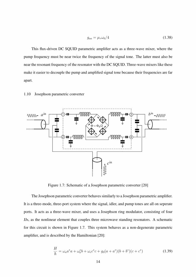
1.10 Josephson parametric converter
Figure 1.7: Schematic of a Josephson parametric converter [20]
The Josephson parametric converter behaves similarly to a Josephson parametric amplifier.
It is a three-mode, three-port system where the signal, idler, and pump tones are all on seperate
ports. It acts as a three-wave mixer, and uses a Josephson ring modulator, consisting of four
JJs, as the nonlinear element that couples three microwave standing resonators. A schematic
for this circuit is shown in Figure 1.7. This system behaves as a non-degenerate parametric
amplifier, and is described by the Hamiltonian [20]:
H
h= ωaa
∗a+ ω∗b b+ ωcc∗c+ g3(a+ a∗)(b+ b∗)(c+ c∗) (1.39)
14

together with their port couplings Ka, Kb, and Kc. The frequency scales are such that
ωc >> ωb > ωa > Kc >> Ka ' Kb >> g3 (1.40)
This trilinear coupling term is treated as a perturbation, and unlike the Kerr nonlinearity
does not offset the frequency of the quadratic terms at the lowest order. In this Hamiltonian,
terms of higher order are neglected to ensure that the system remains stable under large am-
plitudes. While this system is not simulated in this thesis, it is briefly discussed in Chapter
4.
1.11 Traveling-wave parametric amplifier
Figure 1.8: Schematic of traveling-wave parametric amplifier [21]
In a traveling-wave parametric amplifier, the signal and idler originally act as uncoupled
harmonic oscillators. These modes are then coupled via a parameter that oscillates harmoni-
cally at a frequency equal to the sum of the two modes’ frequencies [21]–[23]. An example of
such an amplifier is shown in Figure 1.8.
If the externally applied pump mode’s frequency is equal to the sum of two resonant signal
and idler modes, the latter two modes are forced into a closely coupled oscillation. The signal
and idler modes become more amplified the further along they are in the circuit. The gain is
15

periodic and has a maximum limit, and the gain of the signal is greater than the gain of the
idler.
It is usually preferable for the phase mismatch of the pump and signal to be lower than the
modulation depth of the nonlinear parameter, as the signal gain increases exponentially with
respect to circuit distance. The mismatch should be as close to the modulation depth as possible
to achieve the highest gain. If there is no mismatch, i.e. the pump’s phase constant is equal to
the sum of the signal and idler’s phase constants, the input signal is amplified in the form of a
growing wave.
1.11.1 Four-wave mixing
As stated earlier, a Josephson junction can provide the nonlinearity need for wave-mixing
and parametric amplification. One such amplifier uses a design based on a nonlinear transmis-
sion line containing capacitively shunted Josephson junctions [21]. Each “node” in this circuit
consists of one capacitively shunted Josephson junction and its respective coupling capacitor.
The current conservation in each node is given by:
In = I(Cj),n + IL,n (1.41)
The Josephson current is given by:
IL,n = IJ sin[Φn
ϕ0
] (1.42)
Where Ij is the critical current and ϕ0 = Φ0/(2π) is the reduced flux quantum. The
signal gain is increased as the length of the circuit, i.e the number of nodes, is increased. This
four-wave mixing method requires a large pump tone, and it is more difficult to separate the
amplified signal from the pump tone.
Since the pump is so strong, the phase velocities are modified through self and cross-phase
modulation, creating a phase mismatch and preventing exponential gain. As such, the four-
wave mixing regime is generally less desired than the three-wave mixing regime. However,
16

the four-wave mixing regime is easier to implement as it does not require any biasing for its
SQUIDs.
For three-wave mixing, the bias flux must be specifically designed such that ϕdc = (n +
1/2)π, which usually necessitates a fine level of precision according to the Josepshon junction
characteristics and the circuit parameters.
1.11.2 Three-wave mixing
As stated before, the JTWPA consists of a serial array of one-junction rf SQUIDs embed-
ded in a superconducting transmission line. By applying an external magnetic flux to these
SQUIDs, one can control the shape of their current-phase relation. This dc flux bias can be set
such that the amplifier operates in the three-wave mixing mode with minimal phase mismatch
[24]. An example of this amplifier is shown in Figure 1.9. The pump frequency is shifted away
from the signal and can be efficiently filtered out from the amplified signal.
The current-phase relation of a rf SQUID is given by the formula:
I(ϕ) = Ic[ϕ
βL− sin(ϕdc + ϕ)− sin(ϕdc)] (1.43)
The current is described by the formula:
I(ϕ) = Ic[ϕ
βL− sin(ϕdc)(
ϕ2
2) + cos(ϕdc)(ϕ−
ϕ3
6)] (1.44)
Figure 1.9: Schematic of traveling-wave parametric amplifier for the three-wave regime [24]
17

When there is no bias, i.e. ϕdc = 0, nπ, Equation 1.14 is centrosymmetric and the ampli-
fier operates in the four-wave regime. With the external dc flux bias, Equation 1.14 becomes
noncentrosymmetric.
If the bias is set such that ϕdc = (n + 1/2)π, the cubic term vanishes and the ampli-
fier operates in the three-wave regime. This introduces quadratic nonlinearity along with the
conventional Kerr nonlinearity of a thin superconducting line and provides the asymmetry nec-
essary for three-wave mixing.
These amplifiers can achieve signal gains of over 20dB with fewer circuit nodes than the
number needed for four-wave regime traveling wave amplifiers. Three-wave amplifiers can also
achieve gain over a wider bandwidth of over 5 GHz. The three-wave regime has an inherently
stronger quadratic interaction as opposed to the higher-order cubic interaction in the four-wave
regime, and the former regime can be operated with less pumping power.
In both regimes, the nonlinearity is provides by the nonlinear inductance of the embedded
Josephson junctions. Similarly, the nonlinear capacitance of a QPSJ can provide the nonlinear-
ity for in LC-ladder based traveling wave parametric amplifiers.
1.12 SQUID-based parametric amplifier
Figure 1.10: Simple schematic of a DC SQUID [25]
Some quantum parametric amplifiers use a superconducting transmission-line resonator
terminated by a DC SQUID as opposed to the TWPA that combines the resonator and the
18

Figure 1.11: Schematic of flux-driven parametric amplifier [11]
Josephson junctions [11], [26], [27]. A magnetic flux through the SQUID can modulate the
resonant frequency of the resonator as whole due to the nonlinear inductance of the Josephson
junctions.
Another difference is that the signal and the pump are applied to different ports. The signal
is input to the resonator, whereas the pump into a separate line that is inductively coupled to the
SQUID. A simple schematic of a DC SQUID is shown in Figure 1.10. The pump modulates
the magnetic flux through the SQUID, thus modulating the Josephson nonlinear inductance and
the resonant frequency of the resonator. A schematic of this flux-driven amplifier is shown in
Figure 1.11.
The initial resonant frequency is set by applying an additional DC flux to the SQUID. This
can been done by including an addition DC flux bias line inductively coupled to the SQUID, and
by capacitively coupling the pump and DC flux bias to the same induction line. The signal is
applied near the resonant frequency, and the pump is applied at double the resonant frequency.
In this type of amplifier, the resonant frequency is the parameter that amplifies the signal.
The resonant frequency is modulated periodically about its static dc flux bias value, and thus
the gain has a periodic dependence with a period of π. The amplified signal is reflected back to
its input port.
19

Flux-driven JPAs are desirable because their band center (i.e. the resonant frequency) is
widely tunable [28]. JPAs generally have a small dynamic range, and the gain is saturated for
large input signals. This limits the amplification to signals which contain only a few photons
per bandwidth. Resonator-based parametric amplifiers work in a narrow band, so it is desirable
to match the band of amplification with the frequency of the input signal.
Another positive of these types of JPAs is that the pump and the signal is applied to differ-
ent ports, rather than sharing the same input port as in TWPAs [11]. This makes the separation
of the pump from the output signal much more straightforward.
20

Chapter 2
Traveling-wave parametric amplifiers
Traveling-wave parametric amplifiers are designed as microwave transmission lines en-
abling the mixing of propagating microwaves via a nonlinear parameter, such as the resonator’s
inductance or capacitance. The TWPAs shown here are based on LC-ladder transmission lines,
where the inductors are replaced by JJs or the capacitors are replaced by QPSJs. The pump and
signal are input in the same line, and the signal is amplified as it travels down the circuit. These
introduce the amplifiers’ nonlinearities via the Josephson current-phase relation or the quantum
phase-slip voltage-charge relation. JJ and QPSJ models are used in WRspice to simulate the
behavior of these TWPAs [28].
2.1 Current JJ-based traveling-wave parametric amplifiers
Josephson traveling-wave parametric amplifiers are among the most widespread in the
field [19]. They are commonly implemented as four-wave mixers, where there is no DC current
bias. However, these parametric amplifiers can be operated as three-wave mixers by finding the
appropriate DC bias point, usually done with a DC flux bias line.
Traveling-wave parametric amplifiers do not have a fundamental gain-bandwidth con-
straint. However, in real use the operating bandwidth is limited by dispersion due to the non-
linearity of the JJs [29]. This imposes a stricter constraint on the signal, idler, and pump wave
vectors and the self and cross-phase modulation that arises from the Josephson nonlinear mode
coupling terms.
One research group has successfully demonstrated a strategy to compensate for this dis-
persion problem by periodically loading the transmission line with compact lumped-element
21

Figure 2.1: Band structure of resonantly phase matched and periodically loaded TWPAs. Theparametric amplifier without a resonant element [(a), black only], with a resonant element [(a),black and red], and with periodic loading (b): every 37th unit cell has a slightly different capac-itance and inductance (green). (c) The wave vector as a function of frequency for the TWPA(black dashed line), RPM TWPA (red line), and TWPA with periodic loading (green lines). Theyellow shaded region indicates the photonic band gap due to the periodic loading. The maindifference between the photonic band gap and the resonator is the edge of the Brillouin zone.[11]
resonators [11]. A graphic of this circuit is shown in Figure 2.1. These devices have several
gigahertz of usable bandwidth, and can handle input signal powers of about -100 dBm.
2.2 Directionality
Traveling-wave parametric amplifiers are inherently directional [19]. They produce gain
in the direction in which the pump wave is propagating. In the opposite direction, an ideal
traveling-wave parametric amplifier has unity transmission. However, in real use there is some
finite attenuation due primarily to dielectric losses overlap capacitors. This means that, in
principle, intervening circulators or isolators are not strictly necessary, although a directional
coupler is needed at the input to inject high-power pumps into the input port.
22

In simulations of the traveling-wave parametric amplifier, the measured gain of the signal
tone can be different depending on where in the amplifier the output signal is analyzed. In this
thesis, the output signal is taken at the 100th to last node in the circuit.
2.3 JJ-based traveling-wave parametric amplifier
Figure 2.2: Circuit schematic showing three cells of an N-cell array of RF SQUIDs imple-mented in a microwave transmission line design. The dotted line highlights one of the repeatingcell nodes [11]
The Josephson traveling-wave parametric amplifier is designed as a nonlinear transmission
line [11]. It has an LC-ladder structure, where the inductors are replaced with JJs. The nonlinear
inductance of the JJs is what allows for the wave-mixing of the pump and signal tones and
parametric amplification of the signal tone.
A DC bias can also be applied to the JJs to control whether the JTWPA acts in the four-
wave mixing or three-wave mixing regime. This can take the form of an additional DC current
input into the JJ, or by applying an external magnetic field to the JJs. An example of a JTWPA
is shown in Figure 2.2.
2.3.1 Simulation circuit design
Due to the high number of repeating nodes in the circuit, a Python program is used to create
the circuit files. Each node consists of a JJ, a parallel inductor, and a capacitor connected to
ground each side. Each node also has its own DC bias line, which is coupled to the JJs’ parallel
inductor. The bias current is the same across all nodes. The pump and the signal are input into
the circuit via the same current source. The circuit is terminated by a 50Ω impedance. Unless
23

Isignal + Ipump
50fF
Icrit
57pH
Ibias 57pH
50fF 50fF
Icrit
57pH
50fF
Ibias 57pH
50Ω
Figure 2.3: JTWPA circuit, adapted from [11]
otherwise stated, the DC flux bias is 14µA and the JJ critical current is 5µA. An example of a
circuit node is shown in Figure 2.3. All simulations shown in this thesis were done in WRspice
[30].
The output of the circuit can be taken at any node in the nonlinear transmission line, but
in most of these simulations the output is taken at the hundredth to last node in order to get the
highest possible gain.
2.4 Simulation results
The output was taken all nodes of a 500 node JTWPA. The results are shown in Figure
2.4. The signal tone was input at 0.1 µA at 7.2 GHz and the pump tone was input at 1.97µA
at 12 GHz. The idler tone is 4.8GHz, the signal tone is 7.2 GHz, and the pump tone is 12GHz.
Note that in a TWPA the signal and pump are input along the same line, and thus the wave-
form here is bigger than the signal tone (0.1µA signal amplitude and 1.97µA amplitude). The
simulation shows amplification of the signal tone and the creation of an idler tone at 4.8 GHz,
demonstrating three-wave mixing.
2.4.1 Circuit length
For the JTWPA, the gain of the signal tone generally increases as the length (i.e. the
number of nodes) increases. The node count was increased from 500 to 600 in WRspice. The
24

1 0 0
2 0 0
3 0 0
4 0 0
2 . 4 G H zfi fs 9 . 6 G H z
fp 1 4 . 4 G H zfp + ifp + s
2 1 . 6 G H zf2 p 2 6 . 4 G H z
f2 p + if2 p + s
3 3 . 6 G H zf3 p 3 8 . 4 G H z
f3 p + i f3 p + s 4 5 . 6 G H zf4 p 5 0 . 4 G H z
f4 p + i f4 p + s5 7 . 6 G H z
f5 p
0 . 00 . 20 . 40 . 60 . 81 . 01 . 21 . 41 . 61 . 82 . 0
F r e q u e n c y ( G H z )
N o d e n
Figure 2.4: Top: JTWPA spectrum output. The signal tone is input at 0.1 µA at 7.2 GHz and thepump tone is input at 1.97µA at 12 GHz. The idler tone is 4.8GHz, the signal tone is 7.2 GHz,and the pump tone is 12GHz. These results demonstrate three-wave mixing, as fp = fs + fi.Bottom: 3D plot of JTWPA spectrum output.
25

Figure 2.5: JTWPA current output vs. node count
signal tone was input at 0.1 µA at 7.2 GHz and the pump tone was input at 1.97µA at 12
GHz. For each simulation run, the current output at the 100th to last node was recorded, and
the signal tone’s amplitude was subsequently found via a Fourier transform. The results are
shown in Figure 2.5. The results showed several spikes in the signal tone’s gain, and produced
deamplification of the signal tone at around lengths 520-530, 536-538, and 548-552. A JTWPA
with a high node count can produce large gain in the signal tone, but also leads to more layout
and fabrication concerns.
2.4.2 Bias current
The rest of the JTWPA simulations were done with a 500-node circuit, and the current
output at the 100th to last node was analyzed. The signal tone was input at 0.1 µA at 7.2 GHz
and the pump tone was input at 1.97µA at 12 GHz. For each node in the circuit, a corresponding
flux-bias was coupled with the JJ. To simulate this coupling, an inductor was included in series
to the bias current and parallel to the JJ. The bias current was swept from 0 to 25µA, and a
26

Figure 2.6: JTWPA current output vs. DC bias current
Fourier transform was performed on the output current to get the signal tone’s amplitude. The
results are shown in Figure 2.6. The results demonstrate how important this bias current is to
the JTWPA, as the signal’s gain is very sensitive to small differences in the bias current. The
bias current is crucial to whether the amplifier operates in the three-wave or four-wave regime.
2.4.3 Critical current
The critical current of all JJs in the circuit was swept from 0 to 20µA. The signal tone was
input at 0.1 µA at 7.2 GHz and the pump tone was input at 1.97µA at 12 GHz. The results are
shown in Figure 2.7. At values below around 0.5µA, the critical current was found to be too
low for the circuit to operate properly, as the simulations gave illegible results. As, such data
in this range is not shown in the result plot. Past the value, we started seeing many amplitude
peaks and dips. The critical current has a similar effect on the JTWPA as the bias current, as
both affect the centrosymmetry of the circuit and determine whether the amplifier is undergoing
three-wave or four-wave mixing.
27

Figure 2.7: JTWPA current output vs. JJ critical current.
2.5 QPSJ-based traveling-wave parametric amplifier
The QPSJ-based TWPA’s structure is similar to the JTWPA. It has an LC-ladder structure,
but the capacitors are replaced with QPJS instead of replacing the inductors with JJs. Since the
voltage-charge relation of the QPSJ is the dual to the current-phase relation of the JJ, the QPSJ
has a similar nonlinear affect on the transmission line. The nonlinear capacitance of the QPSJs
is what causes the wave-mixing of the pump and signal tones and parametric amplification of
the signal tone. Whereas the JJs in the JTWPA are biased by an external flux, these QPSJs are
bias by connecting an additional DC voltage source to each. This bias voltage is used to control
whether the amplifier operates in the four-wave or three-wave mixing regime.
2.5.1 Simulation circuit design
A similar Python program used to produce the JTWPA circuit file is used for the QPSJ-
based TWPA [15]. Each node consists of a center inductor, with two QPSJs on each side
28

− +
Vsignal + Vpump
Vcrit
−+Vbias
57pH 57pH
Vcrit
−+ Vbias
Vcrit
−+ Vbias
57pH 50Ω
Figure 2.8: QPSJ-based TWPA circuit
connected to ground. If the bias voltage is being tested, a DC voltage source is added between
each QPSJ and ground. An schematic of a QPSJ-based TWPA node is shown in Figure 2.8.
The pump and the signal are input into the circuit via the same voltage source, and the
circuit is terminated by a 50Ω impedance. Unless otherwise stated, the critical voltage of each
QPSJ is 10µV and the bias voltage is set to 0V. As with the JTWPA simulations, the voltage
output is taken at the hundredth to last node in order to get the highest possible gain.
2.6 Simulation results
The output here was taken at all nodes of a 500 node QPSJ-based TWPA. The signal tone
was input at 0.1 µV at 7.2 GHz and the pump tone was input at 1.97µV at 12 GHz. Just like
the JTWPA, with a TWPA the signal and pump are input along the same line, and thus the
waveform here is bigger than the signal tone (0.1µV signal amplitude and 1.97µV amplitude).
The results are shown in Figure 2.9. The simulation shows amplification of the signal tone and
the creation of an idler tone at 16.8 GHz, demonstrating four-wave mixing.
2.6.1 Circuit length
The circuit length should have the same effect on the QPSJ-based TWPA as it does for the
JTWPA. For the QPSJ-based TWPA, the gain of the signal tone increases as the length (i.e. the
number of nodes) increases.
29

1 0 0
2 0 0
3 0 0
4 0 0
fs fp fi
3 1 . 2 G H zf3 p
0 . 00 . 20 . 40 . 60 . 81 . 01 . 21 . 41 . 61 . 82 . 0
F r e q u e n c y ( G H z )
N o d e n
Figure 2.9: Top: QPSJ-based TWPA spectrum output. The signal tone was input at 0.1 µVat 7.2 GHz and the pump tone was input at 1.97µV at 12 GHz. The idler tone is 16.8GHz,the signal tone is 7.2 GHz, and the pump tone is 12GHz. These results demonstrate four-wavemixing, as 2fp = fs + fi. Bottom: 3D plot of QPSJ-based TWPA spectrum output.
30

Figure 2.10: QPSJ-based TWPA voltage output vs. node count
The node count was increased from 500 to 600 in WRspice. For each simulation run,
the voltage output at the 100th to last node was recorded, and the signal tone’s amplitude was
subsequently found via a Fourier transform. The signal tone was input at 0.1 µV at 7.2 GHz
and the pump tone was input at 1.97µV at 12 GHz. The results are shown in Figure 2.10. The
signal tone’s gain increased from 500 to about 515, but afterwards it decreases until about 580
nodes.
2.6.2 Bias voltage
The rest of the QPSJ-based TWPA simulations were done with a 500-node circuit, and
the voltage output at the 100th to last node was analyzed. For each QPSJ in the circuit, a DC
voltage source was included between the QPSJ and ground.
Each of these DC voltage sources was swept from 0 to 5µV, and a Fourier transform was
performed on the output voltage to get the signal tone’s amplitude. The signal tone was input at
0.1 µV at 7.2 GHz and the pump tone was input at 1.97 µV at 12 GHz. The results are shown
31

Figure 2.11: QPSJ-based TWPA voltage output vs. DC bias voltage
in Figure 2.11. The gain of the signal tone slightly increases with increasing bias voltage, but
sharply drops off at around 3.5 µV. Voltages 3.5 µV and below are small compared to the 10
µV QPSJ critical voltages, and thus are not as influential on the signal gain. If the bias is
too high, then the voltage across the QPSJ could fluctuate below the critical voltage and cause
deamplification of the signal.
2.6.3 Critical voltage
The critical voltage of all QPSJs in the circuit was swept from 0 to 20µV. The results are
shown in Figure 2.12. The signal tone was input at 0.1 µV at 7.2 GHz and the pump tone was
input at 1.97µV at 12 GHz. At values below about 3µV, the critical voltage was found to be
too low for the circuit to operate properly, as the simulations gave illegible results. Past the
value, the QPSJ-based TWPA behaves somewhat similarly to the JTWPA, as the signal gain
has multiple peaks and dips. However, the QPSJ variant is not as sensitive to changes in the
critical voltage as the JTWPA is to changes in the critical current.
32

Figure 2.12: QPSJ-based TWPA voltage output vs. QPSJ critical voltage
33

Chapter 3
Lumped-element parametric amplifier
These parametric amplifiers include a controllable, nonlinear element at the end of a res-
onator. Unlike the TWPAs, where the pump and signal tones are at the same input, they are on
separate inputs. The signal current is input into the resonator, and the pump current modulates
the nonlinear termination element. The resonant frequency is thus modulated along with the
nonlinear element, which leads to the parametric amplification of the signal tone. The amplified
signal tone is reflected back along the resonator [8].
Whereas the TWPAs’ output can be taken at a desired node in the transmission line, the
incident and reflected signal tones in these amplifiers must be separated. These amplifiers are
highly dependent on the relative phase between the pump and the signal, and generally have
higher gain bandwidths than their TWPA counterparts.
3.1 Phase dependency
Flux-driven parametric amplifiers are degenerate parametric amplifiers which amplify one
of the two quadratures of a signal with quantum-limited noise.
These amplifiers consist of a superconducting transmission-line resonator terminated by
a DC SQUID. The transmission-line resonator is defined by its coupling capacitance CC . The
magnetic flux φ penetrating the SQUID loop changes the boundary condition of the resonator
at the right end, which enables control of the resonant frequency.
One research group created an amplifier has a maximum amplification of 17 dB and a
noise temperature of less than 0.87 K [21]. One important feature of this amplifier is that its
34

Figure 3.1: (a) Sideband peak of the signal tone, located at 10.78 GHz + 10 kHz (signal tonefrequency + modulation). The solid curve is a spectrum when the pump is on, while the dashedcurve is a spectrum when the pump is off. (b) Gain as a function of the carrier phase of thesignal [21]
35

gain is highly dependent on the phase difference between the signal and pump tones. This is
shown in Figure 3.1.
The results shown in 3.1 from the group defines the gain as the difference between the
two sideband peak values. The gain shows a periodic dependence (π) on the carrier phase of
the signal relative to the pump phase. The phase differences between the two nodes can decide
whether the circuit is in the amplification or deamplification mode.
3.2 JJ-based flux-driven parametric amplifiers
Isignal 16fF0.4264nH
0.4pF
Ipump
5pH
Figure 3.2: Flux-driven JPA, adapted from [21]. The critical current Icrit of each Josephsonjunction in the SQUID is 1.5µA.
The flux-driven parametric amplifier has a superconducting nonlinear transmission-line
resonator terminated by a SQUID. The SQUID consists of two JJs in parallel, and the flux
through this SQUID is controlled by an externally coupled pump line. The resonant frequency
can also be controlled by an external DC flux bias line, which can be used to control the initial
resonant frequency. A schematic of this circuit is shown in Figure 3.2.
The resonator is capacitively coupled to the signal tone’s input, and the input signal’s
frequency is very slightly modulated away from the resonant frequency. The amplifier can be
operated in the three-wave by applying a pump tone that is double the frequency of the signal
tone.
36

Figure 3.3: Schematic of the Simulink setup using IQ demodulation to separate the incidentand reflected waves
3.2.1 Simulation circuit design
For the purposes of simplicity and efficiency, the LC-ladder resonator is shortened to just
one capacitor and inductor. A coupling capacitor connects the amplifier and the signal input.
The signal tone is first input through a 50Ω impedance transmission line. To simulate
the SQUID loop inductance, two additional inductors are included, one before each JJ in the
SQUID. Each of these inductors is half the total loop inductance. These loop inductors allow
for the simulation of the SQUID’s flux control by coupling each inductor to the inductors on
the pump and flux bias lines.
In real use, a circulator is used to separate the incident signal from the reflected signal.
However, for these simulations the waves are separated using IQ demodulation [31].
3.2.2 Separation of incident and reflected waves
The output of this simulation is taken at the the node between the input transmission
line and the amplifier’s coupling capacitor. The transmission line is modeled in WRspice as
a lossless line with a characteristic impedance of 50Ω. This is included to help provide a
decipherable result in the simulations, as the amplifier’s output would just give the input voltage
source’s waveform otherwise.
Since the output node gives both the incident input signal and amplified reflected signal,
IQ demodulation is used in Simulink to extract the reflected signal and calculate the gain [31].
A block diagram of the Simulink model is shown in Figure 3.3. IQ demodulation is performed
on the original output, with the input signal’s frequency used as the local oscillator. The I
37

waveform is taken taken through a low-pass filter; the resultant waveform is then compared
against the original input waveform in order to determine the amplifier gain.
3.2.3 Simulation results
6 . 0 7 . 2 8 . 4 9 . 6 1 0 . 8 1 2 . 0
0 . 0 0 0
0 . 0 6 4
0 . 1 2 8
0 . 1 9 2
0 . 2 5 6 1
F r e q u e n c y ( G H z )
6 . 0 7 . 2 8 . 4 9 . 6 1 0 . 8 1 2 . 0
0 . 0 0 0
0 . 2 3 0
0 . 4 6 0
0 . 6 9 0
0 . 9 2 0 1
2
F r e q u e n c y ( G H z )
Figure 3.4: Top: Plot of the Fourier transform of the flux-driven JPA input. Peak 1 is locatedat 10.77 GHz + 10KHz, and has a magnitude of 0.25 µA. Bottom: Plot of the Fourier trans-form of the QPSJ-based lumped-element parametric amplifier output. Peak 1 is located at 7.86GHz, and has a magnitude of 0.904 µA. Peak 2 is located at 10.77 GHz + 10KHz, and has amagnitude of 0.455 µA.
38

0 1 0- 0 . 6- 0 . 4- 0 . 20 . 00 . 20 . 40 . 6
T i m e ( n s )
0 1 0- 0 . 1 0- 0 . 0 50 . 0 00 . 0 50 . 1 0
T i m e ( n s )
Figure 3.5: Input and output wave-forms for the flux-driven JPA. The top plot shows the inputincident signal, and the bottom plot shows the output reflected signal.
Figures 3.4 and 3.5 shows the simulation results of the flux-driven amplifier. The plot
shows the reflected, amplified signal wave against the input, incident signal wave. The input
amplitude is 0.1µA and the pump amplitude is 2µA. While the reflected wave has a higher
amplitude than the input, the waveform is not as clean as expected. Preferably, the amplitude
of the reflected wave should be as constant as the incident wave. We plan to look into this issue
further by investigating the noise response of the circuit and refining our IQ demodulation
process.
3.3 QPSJ-based lumped-element parametric amplifier
A QPSJ-based dual to the SQUID can be made by including two series QPSJs, with a
ground capacitor acting as a charge island between them.
This amplifier has a superconducting nonlinear transmission-line resonator terminated by
the QPSJs. The pump line is coupled to the amplifier by including a coupling capacitor between
the QPSJs. This amplifier does not yet have a dual to the DC flux bias.
39

The resonator itself is capacitively coupled to the signal tone’s input, and the input signal’s
frequency is very slightly modulated away from the resonant frequency. The amplifier can be
operated in the three-wave by applying a pump tone that is double the frequency of the signal
tone.
3.3.1 Simulation circuit design
Vsignal 16fF 0.023795pF
0.4264nH Vpump5pF2e/2Vcrit
Figure 3.6: QPSJ-driven lumped-element parametric amplifier. The critical voltage Vcrit ofeach QPSJ is 1.5µV .
As with the flux-driven parametric amplifier, the LC-ladder resonator is shortened to just
one capacitor and inductor. A coupling capacitor connects the amplifier and the signal input.
The signal tone is first input through a 50Ω impedance transmission line.
In addition to the resonator’s capacitor, the QPSJs are included in series with the capac-
itor. In real use, a circulator is used to separate the incident signal from the reflected signal.
However, for these simulations the waves are separated using IQ demodulation.
In the flux-driven amplifier, the pump line is coupled to the nonlinear element by induction.
This is because JJs are current-based and the pump line can apply an external magnetic field
and generate current via the SQUID’s loop inductance. Since this circuit is voltage-based and
uses QPSJs, we instead couple the pump line to the nonlinear element with a capacitor. The
40

pump line can then supply voltage to modulate the charge between the QPSJs. A schematic of
this circuit is shown in Figure 3.6.
3.3.2 Simulation results
6 . 0 7 . 2 8 . 4 9 . 6 1 0 . 8 1 2 . 0
0 . 0 0 0
0 . 0 6 3
0 . 1 2 6
0 . 1 8 9
0 . 2 5 21
F r e q u e n c y ( G H z )
6 . 0 7 . 2 8 . 4 9 . 6 1 0 . 8 1 2 . 00 . 0 0 0
0 . 0 2 9
0 . 0 5 8
0 . 0 8 7
0 . 1 1 6 1
2
F r e q u e n c y ( G H z )
Figure 3.7: Top: Plot of the Fourier transform of the QPSJ-based lumped-element parametricamplifier input. Peak 1 is located at 10.77 GHz + 10KHz, and has a magnitude of 0.25 µV .Bottom: Plot of the Fourier transform of the QPSJ-based lumped-element parametric amplifieroutput. Peak 1 is located at 7.86 GHz, and has a magnitude of 0.111 µV . Peak 2 is located at10.77 GHz + 10KHz, and has a magnitude of 0.0526 µV .
41

0 1 0- 0 . 6- 0 . 4- 0 . 20 . 00 . 20 . 40 . 6
T i m e ( n s )
0 1 0- 0 . 1 0- 0 . 0 50 . 0 00 . 0 50 . 1 0
T i m e ( n s )
Figure 3.8: Input and output wave-forms for the QPSJ-based lumped-element parametric am-plifier. The top plot shows the input incident signal, and the bottom plot shows the outputreflected signal.
Figures 3.7 and 3.8 shows the simulation results of the QPSJ-based amplifier. The input
amplitude is 0.1µV and the pump amplitude is 2µV . The results here are very similar to the
flux-driven amplifier results. The reflected wave has a better amplitude than the input, but the
waveform shows some noise and is not as clean as we would expect. The amplitude of the
reflected wave should be as constant as the incident wave. As with the flux-driven amplifier,
we plan to look into this issue further by investigating the noise response of the circuit and
refining our IQ demodulation process.
42

Chapter 4
Conclusion and future work
While we have made progress in the simulation of quantum parametric amplifiers, there is
still a lot of work left that needs to be done. While many of the experiments shown were work-
ing towards optimizing the gain of our parametric amplifiers, we still have to further analyze
some of the results of our simulation to further understand our circuits, particularly the biasing
of our JJs and QPSJs. We also plan to further explore our lumped-element parametric ampli-
fiers, and try to get cleaner output signals from our simulations. One thing we will try is to
make a SPICE implementation of a JJ or QPSJ-based circulator based on the circuit schematics
in the literature [32]. These schematics are shown in Figure 4.1.
The types of quantum parametric amplifiers shown here are only a sample of those de-
veloped in the field, and we will attempt to simulate these as well, especially the Josephson
parametric converter and parametric amplifiers which use a Josephson ring modulator [32]. An
example of a Josephson ring modulator is shown in Figure 4.2. We also would like to simulate
amplifiers with multiple resonators [33]. The structure of such a circuit shown in Figure 4.3.
We believe we should be able to capture gain in the latter’s simulations as their general layout
is similar to the traveling-wave and lumped-element amplifiers.
One long-term goal in regards to simulating quantum circuits is to capture their photonic
behavior. The simulations shown here only capture the nonlinear behavior of our devices.
Quantum logic circuits have been simulated in WRspice before, and we may be able to incor-
porate the latter designs into the traveling-wave parametric amplifiers to capture more complex
behavior.
43

Figure 4.1: Left: QPS implementation of the circulator using flux tunneling and capacitancebias. Center: Schematic representation of the circulator, consisting of three ports connected viacoupling elements to the numbered nodes of the ring to the coordinate nj associated with nodej. A central ring bias X is conjugate to nj . Right: JJ implementation of the circulator relyingon charge tunneling and inductive bias.[32]
Figure 4.2: (a) Linear inductor with inductance L, capacitor with capacitance C, and a Joseph-son junction with critical current ic. (b) Circuit model for a linear inductance shunted Josephsonring modulator (JRM), shaded in red. The linear inductance shunted JRM is connected withthe capacitors and the input-output ports. (c) Normal modes of the JRM [34]
We also want to incorporate these simulations into other work in our research group as
well. One big advantage of WRspice is that it has a well-defined JJ model that can accept many
different parameters, including its shunt capacitance and resistance. Our group is currently
undergoing multiple JJ fabrication process, and once we get some usable junctions, we can then
characterize them. We can take this information and put it into WRspice to get simulations that
44

are closer to our actual JJs, and get quantum parametric amplifier simulations that are more
accurate to our actual devices. We are also currently trying to fabricate QPSJs, though this is
farther off than our JJs processes.
Figure 4.3: (a) Device micrograph with the series λ/4 transformer with impedance Zλ/4 =45Ω (red), a λ/2 transformer with impedance Zλ/2 = 80Ω (green), and a via-free parallelplate capacitor (purple). (b) Circuit representation of the device. (c) Higher-magnificationmicrograph of the JPA SQUID (blue) and its associated flux line [33]
The simulation results shown in this thesis show that we have simulated signal gain and
frequency mixing in multiple quantum parametric amplifiers. We’ve simulated the JTWPA and
flux-driven JPA behavior in WRspice, and analyzed the effect of certain circuit parameters on
the signal tone gain. We’ve also developed and simulated QPJS-based version of these param-
eters and demonstrated their use in WRspice. As parametric amplifiers continue to be a crucial
part of multiple field, it is important to be able to accurately simulate these circuits. These
simulation methods will continue to be developed, leading to better accuracy and complexity.
45

Bibliography
[1] B. Xiong, X. Li, X.-Y. Wang, and L. Zhou, “Improve microwave quantum illumination
via optical parametric amplifier,” Annals of Physics, vol. 385, pp. 757–768, 2017, ISSN:
0003-4916. DOI: https://doi.org/10.1016/j.aop.2017.08.024. [On-
line]. Available: https://www.sciencedirect.com/science/article/
pii/S0003491617302555.
[2] C. Eichler, Y. Salathe, J. Mlynek, S. Schmidt, and A. Wallraff, “Quantum-limited am-
plification and entanglement in coupled nonlinear resonators,” Phys. Rev. Lett., vol. 113,
p. 110 502, 11 Sep. 2014. DOI: 10.1103/PhysRevLett.113.110502. [Online].
Available: https://link.aps.org/doi/10.1103/PhysRevLett.113.
110502.
[3] E. Flurin, N. Roch, F. Mallet, M. H. Devoret, and B. Huard, “Generating entangled
microwave radiation over two transmission lines,” Phys. Rev. Lett., vol. 109, p. 183 901,
18 Oct. 2012. DOI: 10.1103/PhysRevLett.109.183901. [Online]. Available:
https://link.aps.org/doi/10.1103/PhysRevLett.109.183901.
[4] S. J. Weber, A. Chantasri, J. Dressel, A. N. Jordan, K. W. Murch, and I. Siddiqi, “Map-
ping the optimal route between two quantum states,” Nature, vol. 511, no. 7511, pp. 570–
573, Jul. 2014, ISSN: 1476-4687. DOI: 10.1038/nature13559. [Online]. Available:
https://doi.org/10.1038/nature13559.
[5] N. Roch, M. E. Schwartz, F. Motzoi, C. Macklin, R. Vijay, A. W. Eddins, A. N. Korotkov,
K. B. Whaley, M. Sarovar, and I. Siddiqi, “Observation of measurement-induced entan-
glement and quantum trajectories of remote superconducting qubits,” Phys. Rev. Lett.,
46

vol. 112, p. 170 501, 17 Apr. 2014. DOI: 10.1103/PhysRevLett.112.170501.
[Online]. Available: https://link.aps.org/doi/10.1103/PhysRevLett.
112.170501.
[6] P. Campagne-Ibarcq, L. Bretheau, E. Flurin, A. Auffeves, F. Mallet, and B. Huard, “Ob-
serving interferences between past and future quantum states in resonance fluorescence,”
Phys. Rev. Lett., vol. 112, p. 180 402, 18 May 2014. DOI: 10.1103/PhysRevLett.
112.180402. [Online]. Available: https://link.aps.org/doi/10.1103/
PhysRevLett.112.180402.
[7] L. Zhong, E. P. Menzel, R. D. Candia, P. Eder, M. Ihmig, A. Baust, M. Haeberlein, E.
Hoffmann, K. Inomata, T. Yamamoto, Y. Nakamura, E. Solano, F. Deppe, A. Marx, and
R. Gross, “Squeezing with a flux-driven josephson parametric amplifier,” New Journal
of Physics, vol. 15, no. 12, p. 125 013, Dec. 2013. DOI: 10.1088/1367-2630/
15/12/125013. [Online]. Available: https://doi.org/10.1088/1367-
2630/15/12/125013.
[8] Z. R. Lin, K. Inomata, W. D. Oliver, K. Koshino, Y. Nakamura, J. S. Tsai, and T. Ya-
mamoto, “Single-shot readout of a superconducting flux qubit with a flux-driven joseph-
son parametric amplifier,” Applied Physics Letters, vol. 103, no. 13, p. 132 602, 2013.
DOI: 10.1063/1.4821822. eprint: https://doi.org/10.1063/1.
4821822. [Online]. Available: https://doi.org/10.1063/1.4821822.
[9] J. Stehlik, Y.-Y. Liu, C. M. Quintana, C. Eichler, T. R. Hartke, and J. R. Petta, “Fast
charge sensing of a cavity-coupled double quantum dot using a josephson paramet-
ric amplifier,” Phys. Rev. Applied, vol. 4, p. 014 018, 1 Jul. 2015. DOI: 10.1103/
PhysRevApplied.4.014018. [Online]. Available: https://link.aps.org/
doi/10.1103/PhysRevApplied.4.014018.
47

[10] C. Kutlu, A. F. van Loo, S. Uchaikin, A. N. Matlashov, D. Lee, S. Oh, J. Kim, W.
Chung, Y. Nakamura, and Y. K. Semertzidis, “Characterization of a flux-driven joseph-
son parametric amplifier with near quantum-limited added noise for axion search ex-
periments,” Superconductor Science and Technology, 2021. [Online]. Available: http:
//iopscience.iop.org/article/10.1088/1361-6668/abf23b.
[11] T. Yamamoto, K. Inomata, M. Watanabe, K. Matsuba, T. Miyazaki, W. D. Oliver, Y.
Nakamura, and J. S. Tsai, “Flux-driven josephson parametric amplifier,” Applied Physics
Letters, vol. 93, no. 4, p. 042 510, 2008. DOI: 10.1063/1.2964182. [Online].
Available: https://doi.org/10.1063/1.2964182.
[12] R. Vijay, D. H. Slichter, and I. Siddiqi, “Observation of quantum jumps in a super-
conducting artificial atom,” Phys. Rev. Lett., vol. 106, p. 110 502, 11 Mar. 2011. DOI:
10.1103/PhysRevLett.106.110502. [Online]. Available: https://link.
aps.org/doi/10.1103/PhysRevLett.106.110502.
[13] M. Wakayama, “Simplicity of the lowest eigenvalue of non-commutative harmonic os-
cillators and the Riemann scheme of a certain Heun’s differential equation,” Proceedings
of the Japan Academy, Series A, Mathematical Sciences, vol. 89, no. 6, pp. 69–73, 2013.
DOI: 10.3792/pjaa.89.69. [Online]. Available: https://doi.org/10.
3792/pjaa.89.69.
[14] D. Sank, Z. Chen, M. Khezri, J. Kelly, R. Barends, B. Campbell, Y. Chen, B. Chiaro,
A. Dunsworth, A. Fowler, E. Jeffrey, E. Lucero, A. Megrant, J. Mutus, M. Neeley, C.
Neill, P. J. J. O’Malley, C. Quintana, P. Roushan, A. Vainsencher, T. White, J. Wenner,
A. N. Korotkov, and J. M. Martinis, “Measurement-induced state transitions in a super-
conducting qubit: Beyond the rotating wave approximation,” Phys. Rev. Lett., vol. 117,
p. 190 503, 19 Nov. 2016. DOI: 10.1103/PhysRevLett.117.190503. [Online].
Available: https://link.aps.org/doi/10.1103/PhysRevLett.117.
190503.
[15] U. Goteti, “Spice model implementation of a quantum phase-slip junction,” M.S. thesis,
Auburn University, 2015.
48

[16] J. Matisoo, “Josephson-type superconductive tunnel junctions and applications,” IEEE
Transactions on Magnetics, vol. 5, no. 4, pp. 848–873, 1969. DOI: 10.1109/TMAG.
1969.1066651.
[17] J. E. Mooij and Y. V. Nazarov, “Superconducting nanowires as quantum phase-slip junc-
tions,” Nature Physics, vol. 2, no. 3, pp. 169–172, Mar. 2006, ISSN: 1745-2481. DOI:
10.1038/nphys234. [Online]. Available: https://doi.org/10.1038/
nphys234.
[18] F. D. O. Schackert, “A practical quantum-limited parametric amplifier based on the
josephson ring modulator,” English, Copyright - Database copyright ProQuest LLC;
ProQuest does not claim copyright in the individual underlying works; Last updated
- 2021-04-12, Ph.D. dissertation, 2013, p. 184, ISBN: 978-1-303-71915-8. [Online].
Available: http : / / spot . lib . auburn . edu / login ? url = https : / /
www.proquest.com/dissertations-theses/practical-quantum-
limited-parametric-amplifier/docview/1496062766/se-2?accountid=
8421.
[19] J. Aumentado, “Superconducting parametric amplifiers: The state of the art in josephson
parametric amplifiers,” IEEE Microwave Magazine, vol. 21, no. 8, pp. 45–59, 2020. DOI:
10.1109/MMM.2020.2993476.
[20] A. Roy and M. Devoret, “Introduction to parametric amplification of quantum signals
with josephson circuits,” Comptes Rendus Physique, vol. 17, no. 7, pp. 740–755, 2016,
Quantum microwaves / Micro-ondes quantiques, ISSN: 1631-0705. DOI: https://
doi.org/10.1016/j.crhy.2016.07.012. [Online]. Available: https://
www.sciencedirect.com/science/article/pii/S1631070516300640.
[21] O. Yaakobi, L. Friedland, C. Macklin, and I. Siddiqi, “Parametric amplification in joseph-
son junction embedded transmission lines,” Phys. Rev. B, vol. 87, p. 144 301, 14 Apr.
2013. DOI: 10.1103/PhysRevB.87.144301. [Online]. Available: https://
link.aps.org/doi/10.1103/PhysRevB.87.144301.
49

[22] C. Macklin, K. O’Brien, D. Hover, M. E. Schwartz, V. Bolkhovsky, X. Zhang, W. D.
Oliver, and I. Siddiqi, “A near–quantum-limited josephson traveling-wave parametric
amplifier,” Science, vol. 350, no. 6258, pp. 307–310, 2015, ISSN: 0036-8075. DOI: 10.
1126/science.aaa8525. eprint: https://science.sciencemag.org/
content/350/6258/307.full.pdf. [Online]. Available: https://science.
sciencemag.org/content/350/6258/307.
[23] L. Planat, A. Ranadive, R. Dassonneville, J. Puertas Martınez, S. Leger, C. Naud, O.
Buisson, W. Hasch-Guichard, D. M. Basko, and N. Roch, “Photonic-crystal josephson
traveling-wave parametric amplifier,” Phys. Rev. X, vol. 10, p. 021 021, 2 Apr. 2020. DOI:
10.1103/PhysRevX.10.021021. [Online]. Available: https://link.aps.
org/doi/10.1103/PhysRevX.10.021021.
[24] A. B. Zorin, “Josephson traveling-wave parametric amplifier with three-wave mixing,”
Phys. Rev. Applied, vol. 6, p. 034 006, 3 Sep. 2016. DOI: 10.1103/PhysRevApplied.
6.034006. [Online]. Available: https://link.aps.org/doi/10.1103/
PhysRevApplied.6.034006.
[25] Y. Wang, G. Zhang, S. Zhang, and X. Xie, “Analysis of lc-resonance in dc squid using
dynamic system model,” IEEE Transactions on Applied Superconductivity, vol. 30, no. 8,
pp. 1–7, 2020. DOI: 10.1109/TASC.2020.3024229.
[26] M. A. Castellanos-Beltran and K. W. Lehnert, “Widely tunable parametric amplifier
based on a superconducting quantum interference device array resonator,” Applied Physics
Letters, vol. 91, no. 8, p. 083 509, 2007. DOI: 10.1063/1.2773988. eprint: https:
//doi.org/10.1063/1.2773988. [Online]. Available: https://doi.org/
10.1063/1.2773988.
[27] J. Y. Mutus, T. C. White, E. Jeffrey, D. Sank, R. Barends, J. Bochmann, Y. Chen, Z.
Chen, B. Chiaro, A. Dunsworth, J. Kelly, A. Megrant, C. Neill, P. J. J. O’Malley, P.
Roushan, A. Vainsencher, J. Wenner, I. Siddiqi, R. Vijay, A. N. Cleland, and J. M. Mar-
tinis, “Design and characterization of a lumped element single-ended superconducting
microwave parametric amplifier with on-chip flux bias line,” Applied Physics Letters,
50

vol. 103, no. 12, p. 122 602, 2013. DOI: 10.1063/1.4821136. eprint: https:
//doi.org/10.1063/1.4821136. [Online]. Available: https://doi.org/
10.1063/1.4821136.
[28] J. Y. Mutus, T. C. White, R. Barends, Y. Chen, Z. Chen, B. Chiaro, A. Dunsworth,
E. Jeffrey, J. Kelly, A. Megrant, C. Neill, P. J. J. O’Malley, P. Roushan, D. Sank, A.
Vainsencher, J. Wenner, K. M. Sundqvist, A. N. Cleland, and J. M. Martinis, “Strong
environmental coupling in a josephson parametric amplifier,” Applied Physics Letters,
vol. 104, no. 26, p. 263 513, 2014. DOI: 10.1063/1.4886408. eprint: https:
//doi.org/10.1063/1.4886408. [Online]. Available: https://doi.org/
10.1063/1.4886408.
[29] K. O’Brien, C. Macklin, I. Siddiqi, and X. Zhang, “Resonant phase matching of joseph-
son junction traveling wave parametric amplifiers,” Phys. Rev. Lett., vol. 113, p. 157 001,
15 Oct. 2014. DOI: 10.1103/PhysRevLett.113.157001. [Online]. Available:
https://link.aps.org/doi/10.1103/PhysRevLett.113.157001.
[30] S. Whiteley, “Josephson junctions in spice3,” IEEE Transactions on Magnetics, vol. 27,
no. 2, pp. 2902–2905, 1991. DOI: 10.1109/20.133816.
[31] O. Naaman, D. G. Ferguson, A. Marakov, M. Khalil, W. F. Koehl, and R. J. Epstein,
“High saturation power josephson parametric amplifier with ghz bandwidth,” in 2019
IEEE MTT-S International Microwave Symposium (IMS), 2019, pp. 259–262. DOI: 10.
1109/MWSYM.2019.8701068.
[32] C. Muller, S. Guan, N. Vogt, J. H. Cole, and T. M. Stace, “Passive on-chip supercon-
ducting circulator using a ring of tunnel junctions,” Phys. Rev. Lett., vol. 120, p. 213 602,
21 May 2018. DOI: 10.1103/PhysRevLett.120.213602. [Online]. Available:
https://link.aps.org/doi/10.1103/PhysRevLett.120.213602.
[33] J. Grebel, A. Bienfait, E. Dumur, H.-S. Chang, M.-H. Chou, C. R. Conner, G. A. Peairs,
R. G. Povey, Y. P. Zhong, and A. N. Cleland, “Flux-pumped impedance-engineered
broadband josephson parametric amplifier,” Applied Physics Letters, vol. 118, no. 14,
p. 142 601, 2021. DOI: 10.1063/5.0035945. eprint: https://doi.org/10.
51

1063/5.0035945. [Online]. Available: https://doi.org/10.1063/5.
0035945.
[34] C. Liu, T.-C. Chien, M. Hatridge, and D. Pekker, “Optimizing josephson-ring-modulator-
based josephson parametric amplifiers via full hamiltonian control,” Phys. Rev. A, vol. 101,
p. 042 323, 4 Apr. 2020. DOI: 10.1103/PhysRevA.101.042323. [Online]. Avail-
able: https://link.aps.org/doi/10.1103/PhysRevA.101.042323.
52

Appendices
53

Appendix A
Simulation programs
A.1 JTWPA Python code
import sys
import os
import numpy as np
int2 = 2
int125002 = 125002
int555555 = 555555
int1 = 1
int5001 = 5001
i = 0
x = 0
biasA = 0.1
fftinput = []
signal = 0.001
induc = 0
icrit = 0.1
length = 500
while length < 601:
outfile = open("/home/kmk0046/run5.cir", "w")
54

outfile.write("*jj bias sweep\n")
outfile.write(".model jj0 jj(rtype=0, icrit=5uA, cap
→ =60.0000fF)\n")
outfile.write("Iin 1 0 (sin(0 1.97uA 12.0000GHz 9ns 0 0) +
→ sin(0 0.1uA 7.2000GHz 9ns 0 0))\n")
while i < length:
line1 = "Idc" + str(int2) + " 0 " + str(int125002) + "
→ pwl(0 0uA 5ns 14.0680uA)\n"
line2 = "Lflux" + str(int2) + " " + str(int125002) + " 0
→ 57.0000pH\n"
line5 = "Lg" + str(int2) + " " + str(int1) + " " + str(
→ int555555) + " 57pH\n"
line3 = "K" + str(int2) + " Lg" + str(int2) + " Lflux" +
→ str(int2) + " 1\n"
line8 = "Cg" + str(int2) + " " + str(int1) + " 0 50fF\n"
line6 = "B" + str(int2) + " " + str(int1) + " " + str(
→ int555555) + " " + str(int5001) + " jj0\n"
line10 = "Vout" + str(int1) + " " + str(int555555) + " "
→ + str(int2) + " DC 0\n"
line7 = "Cgg" + str(int2) + " " + str(int2) + " 0 50fF\n
→ "
# write to file
if i == 0:
outfile.write(line8)
i += 1
continue
outfile.write(line1)
55

outfile.write(line2)
outfile.write(line5)
outfile.write(line3)
outfile.write(line6)
outfile.write(line10)
outfile.write(line7)
outfile.write("\n")
int2 += 1
int125002 += 1
int1 += 1
int5001 += 1
int555555 += 1
i += 1
int125002 = 125002
int5001 = 5001
i = 0
int555555 = 555555
outfile.write("Rtermend " + str(length) + " 0 50Ohm\n")
outfile.write(".control \n")
outfile.write("set maxdata = 2e9\n")
outfile.write("tran 1p 22.0000n 12n uic\n")
outfile.write("print /n i(Vout" + str(length - 100) + ") >
→ /home/kmk0046/outf5.txt\n")
int2 = 2
int1 = 1
outfile.write("set noaskquit\n")
outfile.write("quit\n")
56

outfile.write(".endc\n")
outfile.close()
os.system("wrspice /home/kmk0046/run5.cir")
with open("/home/kmk0046/outf5.txt", "r") as f:
for line in f:
fftinput.append(float(line))
f.close()
fftresult = np.fft.fft(fftinput)
n = len(fftinput)
P2 = abs(fftresult/n)
P1 = P2[0:(n//2)+1]
P1[1:len(P1)-1] = 2 * P1[1:len(P1)-1]
freq = np.fft.rfftfreq(n, 0.000000000001)
result = open("/home/kmk0046/result5.txt", "a")
towrite = str(length) + " "
result.write(towrite)
for x in range(len(P1)):
result.write(str(P1[x]) + " ")
result.write("\n")
result.close()
length += 1
fftinput = []
A.2 QPSJ-based TWPA Python code
import sys
57

import os
import numpy as np
int2 = 2
int125002 = 125002
int1 = 1
int5001 = 5001
i = 0
x = 0
biasV = 0.001
fftinput = []
signal = 0.001
induc = 0
vcrit = 0.001
length = 1
while length < 500:
outfile = open("/home/kmk0046/runx.cir", "w")
outfile.write("*bias\n")
outfile.write(".control\n")
outfile.write("devload /home/kmk0046/qps.so\n")
outfile.write(".endc\n")
outfile.write(".model qps p(level=2, vcrit=10u)\n")
outfile.write("Vin 1 0 (sin(0 1.97uV 12.0000GHz 9ns 0 0) +
→ sin(0 0.1uV 7.2000GHz 9ns 0 0))\n")
while i < 500:
line8 = "Pg" + str(int2) + " " + str(int1) + " " + str(
→ int5001) + " qps\n"
58

line4 = "Vb" + str(int5001) + " " + str(int5001) + " 0
→ pwl(0 0uV 5ns 0uV)\n"
int5001 += 1
line5 = "Lg" + str(int2) + " " + str(int1) + " " + str(
→ int2) + " 57pH\n"
line7 = "Pgg" + str(int2) + " " + str(int2) + " " + str(
→ int5001) + " qps\n"
line9 = "Vbb" + str(int2) + " " + str(int5001) + " 0 pwl
→ (0 0uV 5ns 0uV)\n"
# write to file
if i == 0:
outfile.write(line8)
outfile.write(line4)
int5001 += 1
i += 1
continue
outfile.write(line5)
outfile.write(line7)
outfile.write(line9)
outfile.write("\n")
int2 += 1
int125002 += 1
int1 += 1
int5001 += 1
i += 1
int2 = 2
59

int1 = 1
int5001 = 5001
i = 0
outfile.write("Rtermend 500 0 50Ohm\n")
outfile.write(".control \n")
outfile.write("set maxdata = 8e8\n")
outfile.write("tran 1p 22.0000n 12n uic\n")
outfile.write("print /n v(" + str(length) + ") > /home/
→ kmk0046/outf.txt\n")
outfile.write("set noaskquit\n")
outfile.write("quit\n")
outfile.write(".endc\n")
outfile.close()
os.system("wrspice /home/kmk0046/runx.cir")
with open("/home/kmk0046/outf.txt", "r") as f:
for line in f:
fftinput.append(float(line))
f.close()
fftresult = np.fft.fft(fftinput)
n = len(fftinput)
P2 = abs(fftresult/n)
P1 = P2[0:(n//2)+1]
P1[1:len(P1)-1] = 2 * P1[1:len(P1)-1]
freq = np.fft.rfftfreq(n, 0.000000000001)
result = open("/home/kmk0046/resultqpsjall.txt", "a")
towrite = str(length) + " "
60

result.write(towrite)
for x in range(len(P1)):
result.write(str(P1[x]) + " ")
result.write("\n")
result.close()
length += 1
fftinput = []
A.3 Flux-driven JPA WRspice circuit file
*JPA flux
.model jj1 jj(rtype=1,icrit=1.5ua)
tSignal 23 0 24 0 z0=50 td=1ps
vPump 1 2 DC 0
vSignalin 3 23 DC 0
vSignalout 24 4 DC 0
iPumpin 0 1 sin(0 0.1uA 21.56Hz 0ns 0 0)
iSignal 0 3 sin(0 2uA 10.77001GHz 0ns 0 0)
cc 4 5 16fF
cr 5 0 0.4pF
lg 5 6 0.4264nH
ls1 6 7 17.5pH
ls2 6 8 17.5pH
61

b1 7 0 jj1
b2 8 0 jj1
lp1 2 9 2.5pH
lp2 9 0 2.5pH
k1 ls1 lp1 1
k2 ls2 lp2 1
.control
tran 1p 10.0000n 0n uic
print /n v(3) v(24) > /home/u3/kmk0046/output.txt
.endc
A.4 QPSJ-based lumped-element parametric amplifier WRspice file
*QPSJ
.model qps p(level=2, vcrit=1.5uV)
tSignal 23 0 24 0 z0=50 td=1ps
vPump 1 2 DC 0
vSignalin 3 23 DC 0
vSignalout 24 4 DC 0
vPumpin 0 1 sin(0 0.1uV 21.56Hz 0ns 0 0)
vSignal 0 3 sin(0 2uV 10.77001GHz 0ns 0 0)
cc 4 5 16fF
62

lg 5 0 0.4264nH
cr 5 6 0.023795pF
P1 6 7 qps
cg 7 0 1.0667e-13H
P2 7 0 qps
cpump 7 2 5pF
.control
tran 1p 10.0000n 0n uic
print /n v(3) v(24) > /home/u3/kmk0046/output.txt
.endc
63