shunt active power filter - inflibnetshodhganga.inflibnet.ac.in/bitstream/10603/7439/12/12_chapter...
TRANSCRIPT
51
Chapter 4
Unified Power Quality Conditioner (UPQC)
The aim of a unified power quality conditioner (UPQC) that consists of series active and
shunt active filters is to compensate for supply voltage flicker/imbalance, reactive power,
negative sequence current and harmonics. In other words, the UPQC has the capability of
improving power quality at the point of installation on power distribution systems or
industrial power systems. The UPQC, therefore, is expected to be one of the most
powerful solutions to large capacity loads sensitive to supply voltage flicker/imbalance.
The UPQC can be divided into two parts i.e. general UPQC, for power distribution
systems and industrial power systems; and specific UPQC for a supply voltage
flicker/imbalance sensitive load, which is installed by electric power consumers on their
own premises. In UPQC the series active power filter eliminates supply voltage
flicker/imbalance from the load terminal voltage and forces an existing shunt passive
filter to absorb all the current harmonics produced by a nonlinear load. Elimination of
supply voltage flicker, however, is accompanied by low frequency fluctuation of active
power flowing into or out of series active filter. The shunt active filter performs dc link
voltage regulation, thus leading to a significant reduction of capacity of dc link capacitor.
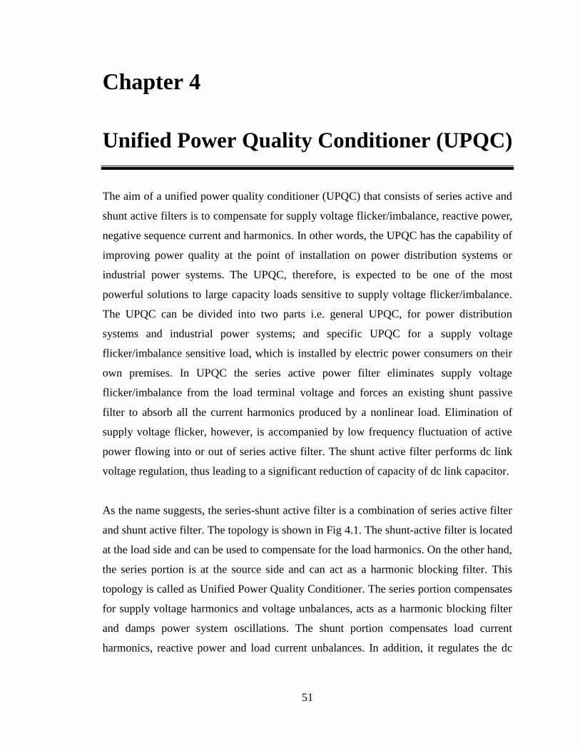
As the name suggests, the series-shunt active filter is a combination of series active filter
and shunt active filter. The topology is shown in Fig 4.1. The shunt-active filter is located
at the load side and can be used to compensate for the load harmonics. On the other hand,
the series portion is at the source side and can act as a harmonic blocking filter. This
topology is called as Unified Power Quality Conditioner. The series portion compensates
for supply voltage harmonics and voltage unbalances, acts as a harmonic blocking filter
and damps power system oscillations. The shunt portion compensates load current
harmonics, reactive power and load current unbalances. In addition, it regulates the dc
52
link capacitor voltage. The power supplied or absorbed by the shunt portion is the power
required by the series compensator and the power required to cover losses [39].
n
Va
Vb
Vc
Ta
Tb
Tc
C1
C2
Series Active Power
Filter
Shunt Active Power
Filter
Nonlinear
Loads
Fig 4.1 Unified Power Quality Conditioner Topology
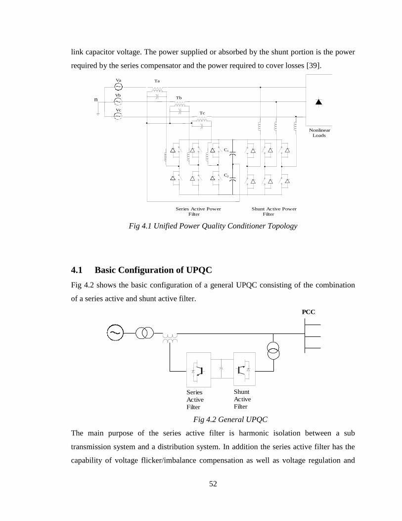
4.1 Basic Configuration of UPQC
Fig 4.2 shows the basic configuration of a general UPQC consisting of the combination
of a series active and shunt active filter.
Series
Active
Filter
Shunt
Active
Filter
PCC
Fig 4.2 General UPQC
The main purpose of the series active filter is harmonic isolation between a sub
transmission system and a distribution system. In addition the series active filter has the
capability of voltage flicker/imbalance compensation as well as voltage regulation and
53
harmonic compensation at the utility-consumer point of common coupling (PCC). The
main purpose of the shunt active filter is to absorb current harmonics, compensate for
reactive power and negative sequence current, and regulate the dc link voltage between
both active filters [40-41].
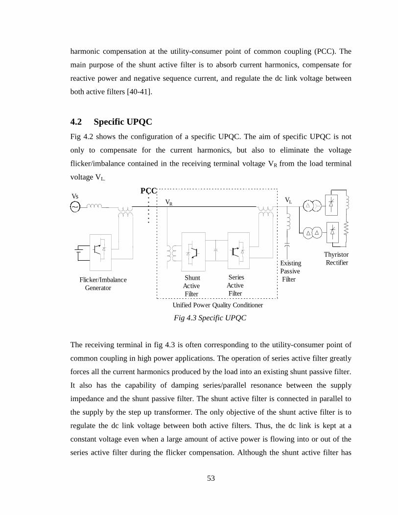
4.2 Specific UPQC
Fig 4.2 shows the configuration of a specific UPQC. The aim of specific UPQC is not
only to compensate for the current harmonics, but also to eliminate the voltage
flicker/imbalance contained in the receiving terminal voltage VR from the load terminal
voltage VL.
PCC
Shunt
Active
Filter
Series
Active
Filter
Existing
Passive
Filter
Thyristor
Rectifier
VsVLVR
Unified Power Quality Conditioner
Flicker/Imbalance
Generator
Fig 4.3 Specific UPQC
The receiving terminal in fig 4.3 is often corresponding to the utility-consumer point of
common coupling in high power applications. The operation of series active filter greatly
forces all the current harmonics produced by the load into an existing shunt passive filter.
It also has the capability of damping series/parallel resonance between the supply
impedance and the shunt passive filter. The shunt active filter is connected in parallel to
the supply by the step up transformer. The only objective of the shunt active filter is to
regulate the dc link voltage between both active filters. Thus, the dc link is kept at a
constant voltage even when a large amount of active power is flowing into or out of the
series active filter during the flicker compensation. Although the shunt active filter has
54
the capability of reactive power compensation, the shunt active filter in fig 4.2 provides
no reactive power compensation in order to achieve the minimum required rating of the
shunt active filter. There is noticeable difference in the installation point of shunt active
filters of figures 4.1 and 4.2. The reason is as follows: In fig 4.1, the shunt active filter
compensates for all the current harmonics produced by nonlinear loads downstream of
the PCC. Therefore, it should be connected downstream of the series active filter acting
as a high resistor for harmonic frequencies. In fig 4.2, the shunt active filter draws or
injects the active power fluctuating at a low frequency from or into the supply, while the
existing shunt passive filter absorbs the current harmonics. To avoid the interference
between the shunt active and passive filters, the shunt active filter should be connected
upstream of the series active filter.
4.3 Mathematical Modeling of UPQC
In this study, the power supply is assumed to be a three-phase, three-wire system. The
two active filters are composed of two 3-leg voltage source inverters (VSI). Functionally,
the series filter is used to compensate for the voltage distortions while the shunt filter is
needed to provide reactive power and counteract the harmonic current injected by the
load. Also, the voltage of the DC link capacitor is controlled to a desired value by the
shunt active filter. There can be negative and zero sequence components in the supply
when a voltage disturbance occurs. The DC link capacitor bank is divided into two
groups connected in series. The neutrals of the secondary of both transformers are
directly connected to the dc link midpoint. In this way, as the connection of both three-
phase transformers is Y/Yo, zero sequence voltage appears in the primary winding of the
series connected transformer in order to compensate for the zero sequence voltage of the
supply system. No zero sequence current flows in the primary side of both transformers.
It ensures the system current to be balanced when the voltage disturbance occurs.
Assuming that the load is non-linear, the power system model considered can be divided
into following units: the power supply system, series active filter and shunt active filter.
These constituent members of the UPQC are modeled separately in this section. First
consider the power supply system. By Kirchhoff‘s law:
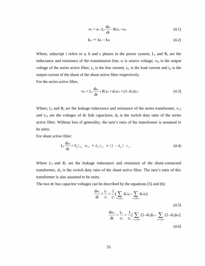
55
is
if i s s is shdi
v = e - L - R i - vdt
(4.1)
is iL ihi = i - i (4.2)
Where, subscript i refers to a, b and c phases in the power system; Ls and Rs are the
inductance and resistance of the transmission line; ei is source voltage; vih is the output
voltage of the series active filter; iis is the line current; iiL is the load current and iis is the
output current of the shunt of the shunt active filter respectively.
For the series active filter,
is
ih 1 1 is 1i c1 1i c2di
v = L + R i + d v + (1-d )vdt
(4.3)
Where, Ll and Rl are the leakage inductance and resistance of the series transformer, vc1
and vc2 are the voltages of dc link capacitors; dli is the switch duty ratio of the series
active filter. Without loss of generality, the turn‘s ratio of the transformer is assumed to
be unity.
For shunt active filter:
ih
2di
Ldt
= R2iih -viF + d2ivcl + (1 - d2i) vc1 (4.4)
Where L2 and R2 are the leakage inductance and resistance of the shunt-connected
transformer, d2i is the switch duty ratio of the shunt active filter. The turn‘s ratio of this
transformer is also assumed to be unity.
The two dc bus capacitor voltages can be described by the equations (5) and (6):
1 1c c
1i is 2i ih
1 1 i=a,b,c i=a,b,c
dv i 1= = ( d i - d i )
dt c c
(4.5)
2 2c c
1i is 2i ih
2 2 i=a,b,c i=a,b,c
dv i 1= = [ (1-d )i - (1-d )i ]
dt c c
(4.6)
56
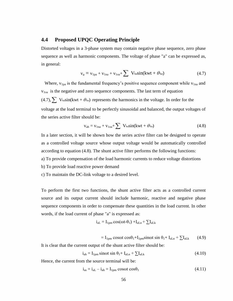
4.4 Proposed UPQC Operating Principle
Distorted voltages in a 3-phase system may contain negative phase sequence, zero phase
sequence as well as harmonic components. The voltage of phase "a" can be expressed as,
in general:
va = v1pa + v1na + v1oa+ ka kaV sin(kwt + ) (4.7)
Where, v1pa is the fundamental frequency‘s positive sequence component while v1na and
v1oa is the negative and zero sequence components. The last term of equation
(4.7), ka kaV sin(kwt + ) represents the harmonics in the voltage. In order for the
voltage at the load terminal to be perfectly sinusoidal and balanced, the output voltages of
the series active filter should be:
vah = v1na + v1oa+ ka kaV sin(kwt + ) (4.8)
In a later section, it will be shown how the series active filter can be designed to operate
as a controlled voltage source whose output voltage would be automatically controlled
according to equation (4.8). The shunt active filter performs the following functions:
a) To provide compensation of the load harmonic currents to reduce voltage distortions
b) To provide load reactive power demand
c) To maintain the DC-link voltage to a desired level.
To perform the first two functions, the shunt active filter acts as a controlled current
source and its output current should include harmonic, reactive and negative phase
sequence components in order to compensate these quantities in the load current. In other
words, if the load current of phase "a" is expressed as:
iaL = I1pm cos(ωt-θ1) +IaLn + ∑IaLk
= I1pm cosωt cosθ1+I1pmsinωt sin θ1+ IaLn + ∑IaLk (4.9)
It is clear that the current output of the shunt active filter should be:
iah = I1pm sinωt sin θ1+ IaLn + ∑IaLk (4.10)
Hence, the current from the source terminal will be:
ias = iaL – iah = I1pm cosωt cosθ1 (4.11)

57
This is a perfect, harmonic-free sinusoid and has the same phase angle as the phase "a"
voltage at the load terminal. The power factor is unity. It means that the reactive power of
load is not provided by the source.
4.5 Design of Proposed UPQC Control model
It is clear from the above discussion that UPQC should first separate out the fundamental
frequency positive sequence from the other components. Then it is necessary to control
the outputs of the two active filters in the way shown in equations (4.8) and (4.10) in
order to improve overall power quality at the load terminal [42, 43].
To solve the first problem, a synchronous d-q-0 reference frame is used. If the 3-phase
voltages are unbalanced and contain harmonics, the transformation to the d-q-0 axes
results in
0 0d a
0 0q b
0 c
v cos(ωt) cos(ωt -120 ) cos(ωt +120 ) v2
v = -sin(ωt) -sin(ωt -120 ) -sin(ωt +120 ) v3
v 1 1 1 v
2 2 2
pm p nm n k k
pm p nm n k k
0m 0
V cos V cos(2ωt + ) 0 V cos(k -1)(ωt + )3
= V sin + -V sin(2ωt + ) + 0 + V sin(k -1)(ωt + )2
0 0 V cos(ωt + ) 0
dp dn dk
qp qn qk
00
v v 0 v
v + v + 0 + v
0 0 v 0
(4.12)
Equation (12) shows that the fundamental positive sequence components of voltages are
represented by dc values in the d-q-0 frame. Here, p is the phase difference between the
positive sequence component and the reference voltage (phase "a‖). For the proper
functioning of a power supply system, it is desirable that the voltages at .the load terminal
should be perfect sinusoids with constant amplitude. Even under a voltage disturbance,
the load still requires a constant voltage. This means that when transformed to the d-q-0
axis, the load voltage become:

58
*
*
*
dF m
qF
0F
v V3
v 02
v 0
(4.13)
Where, Vm is the rated or desired voltage at the load terminal. Only one value, Vm, in the
d-axis would be sufficient to represent the balanced, perfect sinusoidal, 3-phase voltages
in the abc frame. As a reference quantity, it is a known quantity and more suitable for use
in UPQC control than that proposed in [3]. Therefore vdp should be maintained at,
m3 2V while all the other components should be eliminated by the series active filter.
Similar expression can be obtained for the currents:
0 0
0 0
0
cos( ) cos( 120 ) cos( 120 )2
sin( ) sin( 120 ) sin( 120 )3
1 1 1
2 2 2
d a
q b
c
i t t t i
i t t t i
i i
1pm 1 1nm n k k
1pm 1 1nm n k k
I cos I cos(2ωt + ) I cos(k -1)(ωt + )3
= I sin + -I sin(2ωt + ) + I sin(k -1)(ωt + )2
0 0 0
(4.14)
Unlike load voltage, load current can change according to the connected loads. Therefore,
it is not possible to assign it a reference value. Instead, a new "moving time window"
method is applied here to capture the active quantity of the fundamental positive
sequence component which is expressed as a dc value in the d-axis. Furthermore, from
equation (4.14), it is evident that the average of the other components, apart
from 1pm 1I cos , in the d-axis is zero in one fundamental cycle period because all of them
are harmonics of the fundamental. Therefore a time window with a width of 0.02 seconds
(for 50 Hz system) maybe selected to calculate the dc value. The calculation for the first
fundamental cycle is
T
d 1pm 1
0
1i dt = I cos
T . After this, the window is moved forward. If the
moving frequency is also 50 Hz, the delay caused by the calculation is 0.02s. However if
the moving frequency is n times of 50 Hz, the delay will be 0.02/n seconds. As the
window moving frequency increases, calculation delay becomes shorter but the
59
frequency at which the data moving into and out of the window is higher. It may need
longer computation time. Fortunately, in practical power systems, load current changes
slowly. As a compromise, 500 Hz is selected as the window moving frequency in this
paper. The two voltage-source inverters (VSIs) are used as the series and shunt active
filters. The series active filter should behave as a controlled voltage source and its output
voltage should follow the pattern of voltage given in equation (4.8). This compensating
voltage signal can be obtained by comparing the actual load terminal voltage with the
desired value vF*.Since the desired vF* is already defined, it is easy to calculate vh (= vF*
- vs ) as vs is a known quantity. After obtaining the voltage signal vh , the switching duty
ratio of the series active filter is obtained by giving this signal to the hysteresis controller.
The shunt active filter acts as a controlled current source. It means that the inverter
operates in the current-regulated modulation mode. There are various ways to control the
inverter in such a mode, such as the hysteresis control, and predictive control. But in this
thesis work the hysteresis control has been used as given in chapter 6, later in this report.
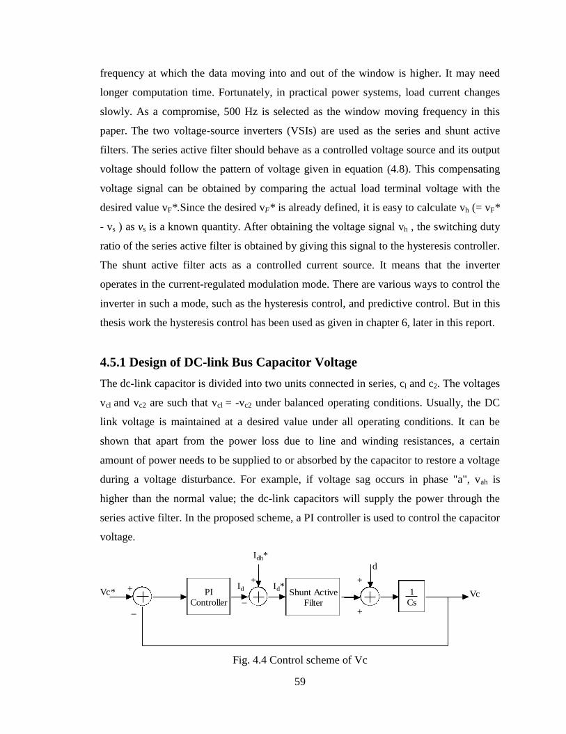
4.5.1 Design of DC-link Bus Capacitor Voltage
The dc-link capacitor is divided into two units connected in series, cl and c2. The voltages
vcl and vc2 are such that vcl = -vc2 under balanced operating conditions. Usually, the DC
link voltage is maintained at a desired value under all operating conditions. It can be
shown that apart from the power loss due to line and winding resistances, a certain
amount of power needs to be supplied to or absorbed by the capacitor to restore a voltage
during a voltage disturbance. For example, if voltage sag occurs in phase "a", vah is
higher than the normal value; the dc-link capacitors will supply the power through the
series active filter. In the proposed scheme, a PI controller is used to control the capacitor
voltage.
PI
ControllerShunt Active
Filter
1
Cs
Vc* +
_
VcId Id*
Idh*
+
_
+
+
d
Fig. 4.4 Control scheme of Vc
60
Fig 4.4 shows the basic control scheme. The input to the PI controller is the error between
the actual capacitor voltage and its desired value. The output of the PI controller is added
to the reference current component in the d axis, id; to form the new reference current id*.
It means that the power needed to charge the two capacitors comes from the active power
of the power supply system. The shunt active filter acts like a regulator. Its currents are
used to adjust the capacitor voltages to within a certain range. Here only one PI controller
is used to control the two capacitor voltages. Although these voltages will not be
symmetrical when the system is unbalanced, this is caused by the zero sequence current
in the UPQC [46].
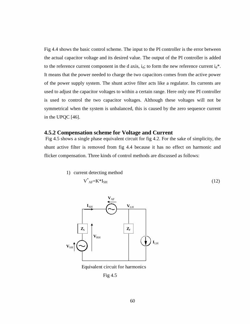
4.5.2 Compensation scheme for Voltage and Current Fig 4.5 shows a single phase equivalent circuit for fig 4.2. For the sake of simplicity, the
shunt active filter is removed from fig 4.4 because it has no effect on harmonic and
flicker compensation. Three kinds of control methods are discussed as follows:
1) current detecting method
V*
AF=K*ISH (12)
ZS ZF
VSH
VRH
VAF
ISH VLH
ILH
Equivalent circuit for harmonics
Fig 4.5
61
2) Voltage detecting method
V*
AF=VRH (13)
3) Combined method
V*RH=K*ISH + VRH (14)
Where K is a proportional gain with a real number.
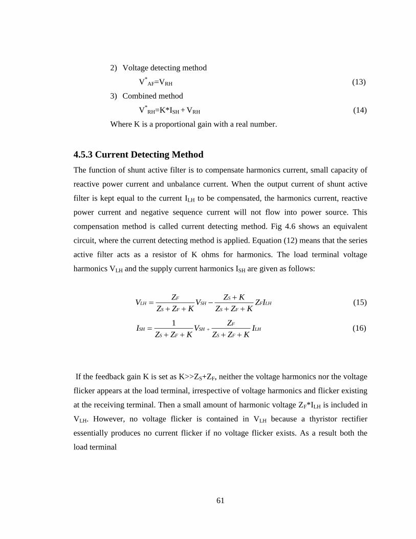
4.5.3 Current Detecting Method
The function of shunt active filter is to compensate harmonics current, small capacity of
reactive power current and unbalance current. When the output current of shunt active
filter is kept equal to the current ILH to be compensated, the harmonics current, reactive
power current and negative sequence current will not flow into power source. This
compensation method is called current detecting method. Fig 4.6 shows an equivalent
circuit, where the current detecting method is applied. Equation (12) means that the series
active filter acts as a resistor of K ohms for harmonics. The load terminal voltage
harmonics VLH and the supply current harmonics ISH are given as follows:
F S
LH SH F LH
S F S F
Z Z KV V Z I
Z Z K Z Z K
(15)
1 F
SH SH LH
S F S F
ZI V I
Z Z K Z Z K
(16)
If the feedback gain K is set as K>>ZS+ZF, neither the voltage harmonics nor the voltage
flicker appears at the load terminal, irrespective of voltage harmonics and flicker existing
at the receiving terminal. Then a small amount of harmonic voltage ZF*ILH is included in
VLH. However, no voltage flicker is contained in VLH because a thyristor rectifier
essentially produces no current flicker if no voltage flicker exists. As a result both the
load terminal
62
Equivalent circuit for current detecting method
ZS ZF
VSH
VRH
VAF
ISH VLH
ILH
K*ISH
Fig. 4.6
voltage and the supply current become purely sinusoidal. It is however difficult to set K
much larger than ZS+ZF for voltage flicker because ZF exhibits high capacitive impedance
at the fundamental frequency. Thus, the current detecting method is not suitable for
voltage flicker compensation.
4.5.4 Voltage Detecting Method
The compensation method for series active filter is called as voltage detecting method.
Fig 4.7 shows an equivalent circuit based on the voltage detecting method given by
equation (13).
Because the output voltage of the series active filter VAF cancels the receiving terminal
voltage harmonics VRH, neither the supply voltage harmonics nor supply voltage flicker
appears at the load terminal, that is,
VLH=0 (17)
However, the existing shunt passive filter loses the capability of trapping current
harmonics produced by the load escape to the supply,

63
ZS ZF
VSH
VRH
VAF
ISH VLH
ILH
Fig. 4.7 Equivalent circuit for voltage detecting method
that is,
ISH=ILH (18)
Thus the voltage detecting method is not suitable for harmonic compensation of the load.
4.5.5 Voltage and Current Combined Method
Fig 4.7 shows an equivalent circuit combining the circuits in figures 4.6 and 4.7 It is clear
from equation (14) that the series active filter looks like a series connection of a voltage
source VRH and resistor K ohms. The receiving terminal voltage harmonics VRH and
supply current harmonics ISH are given by the following:
F
LH LH
F
KZV I
Z K
(19)
F
LH LH
F
ZI I
Z K
(20)
Equivalent circuit for combined method
ZS ZF
VSH
VRH
VAF
ISH VLH
ILH
VRHK*ISH
Fig. 4.8
64
If K is set larger than ZF for harmonics, the combined method can eliminate the supply
current harmonics ISH as effectively as the current detecting method can. Note that the
supply harmonic and/or flicker voltage VSH is excluded from equation (19). The first term
on the right hand side of equation (14) plays an important role in harmonic current
compensation of the load, while the second term contributes to the voltage flicker
cancellation from VLH. Assuming that K is infinite, the output voltage of the series active
filter VAF is given by
lim AF F LH SHK
V Z I V
(21)
The feedback gain K in the combined method can be set lower than that in the current
detecting method because the voltage detecting loop in the combined method
compensates for voltage flicker. The key idea of this control strategy is to obtain the
component to be compensated by subtracting standard wave from the measured waves.
Because the delay of detection and calculation it is difficult for either series active filter
or shunt active filter to realize perfect voltage and current compensation. So the
predictive control method is adopted to improve the compensation effect. It means that
we take the calculated value, the component to be compensated, of the previous period as
the compensating value of the next period, that is
for series active filter
VAF(n+1)
(k)=Vn
SH(k) (22)
and, for shunt active filter
ICF(n+1)
(k)=ILH(n)
(k) (23)
The detection of compensation component:
According to the instantaneous active power definition, we have
pn = vanian + vbnibn + vcnicn where n = 1, 2, 3……….N (24)
Where N is the sampling number per period, the average active power in one cycle can be
given as:
1
1 N
n
n
P pN
(25)
I. Detection of current to be compensated
To detect the current to be compensated, the main problem is to separate active current
component from the whole current. The load current can be divided into two parts, one is
65
the active component, and the other is the current to be compensated, which comprises of
reactive current, harmonic current and negative sequence current. Thus the load current
can be expressed as follows:
iL= i1p+ic (26)
Where il is the load current, i1p is the active component and ic is the current component to
be compensated. In the analysis of the shunt active power filter, we assume that the
system voltage wave is sinusoidal, balanced and symmetrical. The RMS value of phase
voltage and active current can be calculated as
2
1
1 N
n
n
V vN
(27)
IV
(28)
The real time value of fundamental active current can be obtained by the following
equations
ia = V
sinωt
ib =V
sin(ωt- 2π /3) (29)
ic =V
sin (ωt + 2π /3)
But these equations are difficult to be used to calculate the real time current because of
the difficulties of determining the variable t. the active load equivalent resistance;
V
RI
(30)
Where V and I is the RMS value of phase voltage and current. Therefore, we can
obtain the active current with the same frequency and phase shift as the system voltage:
a
apv
iR
b
bpv
iR
(31)
66
c
cpv
iR
Subtracting the currents iap, ibp and icp from detected load current ia, ib and ic
respectively, the current to be compensated can be obtained as:
iac = ia - iap
ibc = ib - ibp (32)
icc = ic - icp
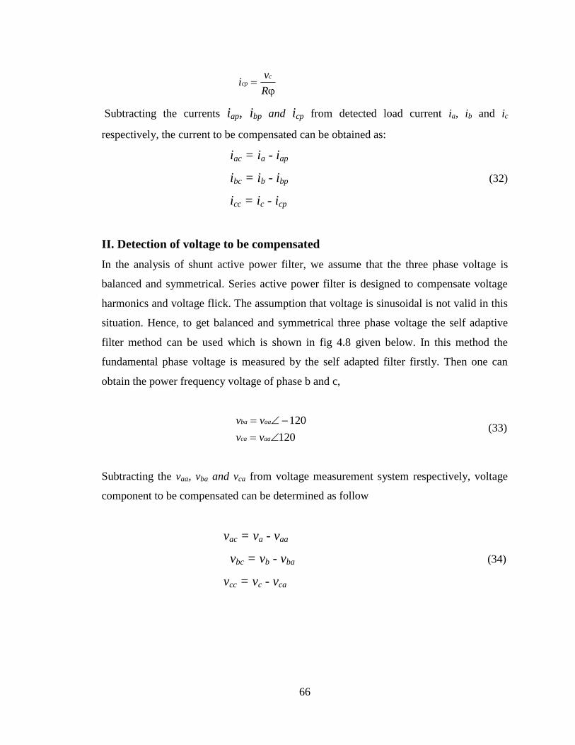
II. Detection of voltage to be compensated
In the analysis of shunt active power filter, we assume that the three phase voltage is
balanced and symmetrical. Series active power filter is designed to compensate voltage
harmonics and voltage flick. The assumption that voltage is sinusoidal is not valid in this
situation. Hence, to get balanced and symmetrical three phase voltage the self adaptive
filter method can be used which is shown in fig 4.8 given below. In this method the
fundamental phase voltage is measured by the self adapted filter firstly. Then one can
obtain the power frequency voltage of phase b and c,
120
120
ba aa
ca aa
v v
v v
(33)
Subtracting the vaa, vba and vca from voltage measurement system respectively, voltage
component to be compensated can be determined as follow
vac = va - vaa
vbc = vb - vba (34)
vcc = vc - vca
67
self adapted
filter
-120
120
va
vb
vc
+
-
+
_
_
+
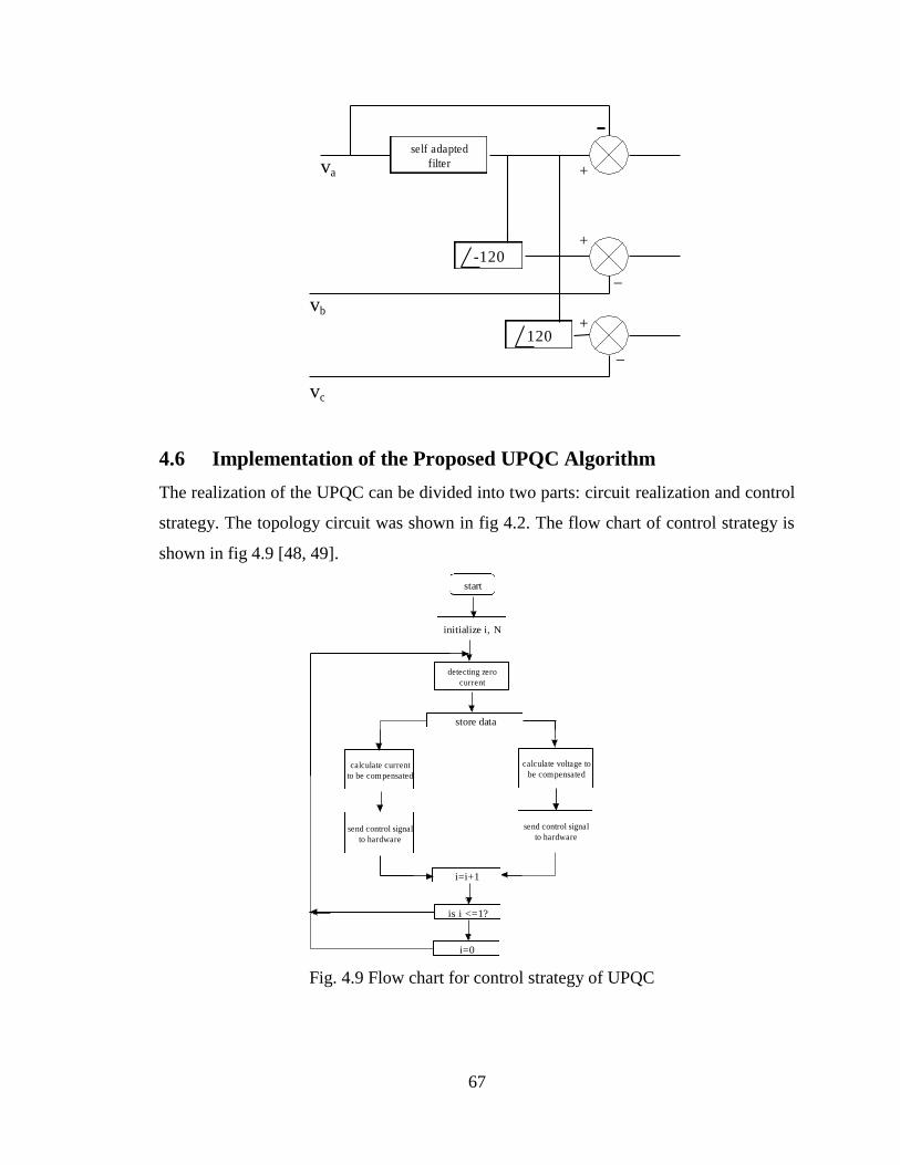
4.6 Implementation of the Proposed UPQC Algorithm
The realization of the UPQC can be divided into two parts: circuit realization and control
strategy. The topology circuit was shown in fig 4.2. The flow chart of control strategy is
shown in fig 4.9 [48, 49].
start
initialize i, N
detecting zero
current
store data
calculate current
to be compensated
calculate voltage to
be compensated
send control signal
to hardware
send control signal
to hardware
i=i+1
is i <=1?
i=0
Fig. 4.9 Flow chart for control strategy of UPQC
68
4.7 Conclusion
In this chapter the unified power conditioner (UPQC) has been discussed in detail. In this
the Mathematical Modeling, Operating Principle and Control scheme of the UPQC have
been discussed in detail. The simulation blocks and their respective results of shunt and
series active power filters and unified power quality conditioner have been shown. A very
simple hysteresis current controller based control technique with help of unit vector
template is proposed for STATCOM. DVR is simulated with abc to dq0 base new control
algorithm to generate the pulse Phase Locked Loop (PLL) is used to generate unit
sinusoidal wave in phase with main voltage. The combination of shunt and series Fact
devices test on the RL load and DC machine