sgls228c –december 2003–revised … voltage detectors 1 features the tps3803g15-q1 device has a...
TRANSCRIPT

ProcessorTPS3805H33-Q1
R1
R2
1.6 V 3.3 V
RESET
GND
VDD
SENSE
RESET
DVDD CVDD
GND
Product
Folder
Sample &Buy
Technical
Documents
Tools &
Software
Support &Community
TPS3803-01-Q1TPS3803G15-Q1, TPS3805H33-Q1
SGLS228C –DECEMBER 2003–REVISED SEPTEMBER 2015
TPS380x-Q1 Voltage DetectorsThe TPS3803G15-Q1 device has a fixed-sense1 Featuresthreshold voltage VIT set by an internal voltage
1• Qualified for Automotive Applications divider, whereas the TPS3803-01-Q1 has an• Single Voltage Detector (TPS3803): Adjustable adjustable SENSE input that can be configured by
and 1.5 V two external resistors. In addition to the fixed sensethreshold monitored at VDD, the TPS3805-Q1 devices• Dual Voltage Detector (TPS3805): Adjustable andprovide a second adjustable SENSE input. RESET is3.3 Vasserted in case either of the two voltages drops
• High ±1.5% Threshold Voltage Accuracy below VIT.• Supply Current: 3 μA Typical at VDD = 3.3 V
During power on, RESET is asserted when supply• Push/Pull Reset Output (TPS3805), voltage VDD becomes higher than 0.8 V. Thereafter,
Open-Drain Reset Output (TPS3803) the supervisory circuit monitors VDD (and/or SENSE)and keeps RESET active as long as VDD or SENSE• Temperature Range: –40°C to 125°Cremains below the threshold voltage VIT. As soon as• 5-Pin SC-70 PackageVDD (SENSE) rises above the threshold voltage VIT,RESET is deasserted again. The product spectrum is2 Applications designed for 1.5-V, 3.3-V, and adjustable supply
• Applications Using DSPs, Microcontrollers, or voltages.Microprocessors The devices are available in a 5-pin SC-70 package.
• Advanced Driver Assistance Systems The TPS3803-Q1 and TPS3805-Q1 devices arecharacterized for operation over a temperature range• Automotive Infotainmentof –40°C to 125°C.• Automotive Cluster
Device Information(1)3 Description
PART NUMBER PACKAGE BODY SIZE (NOM)The TPS3803-Q1 and TPS3805-Q1 families ofTPS3803-01-Q1supervisory circuits provide circuit initialization andTPS3803G15-Q1 SC-70 (5) 2.00 mm × 1.25 mmtiming supervision, primarily for DSPs and processor-
based systems. TPS3805H33-Q1
(1) For all available packages, see the orderable addendum atthe end of the data sheet.
Typical Application Schematic
1
An IMPORTANT NOTICE at the end of this data sheet addresses availability, warranty, changes, use in safety-critical applications,intellectual property matters and other important disclaimers. PRODUCTION DATA.

TPS3803-01-Q1TPS3803G15-Q1, TPS3805H33-Q1SGLS228C –DECEMBER 2003–REVISED SEPTEMBER 2015 www.ti.com
Table of Contents8.2 Functional Block Diagrams ....................................... 91 Features .................................................................. 18.3 Feature Description................................................... 92 Applications ........................................................... 18.4 Device Functional Modes........................................ 113 Description ............................................................. 1
9 Application and Implementation ........................ 124 Revision History..................................................... 29.1 Application Information............................................ 125 Device Comparison Table ..................................... 39.2 Typical Applications ............................................... 126 Pin Configuration and Functions ......................... 3
10 Power Supply Recommendations ..................... 147 Specifications......................................................... 411 Layout................................................................... 157.1 Absolute Maximum Ratings ...................................... 4
11.1 Layout Guidelines ................................................. 157.2 ESD Ratings ............................................................ 411.2 Layout Examples................................................... 157.3 Recommended Operating Conditions....................... 4
12 Device and Documentation Support ................. 177.4 Thermal Information .................................................. 412.1 Device Support .................................................... 177.5 Electrical Characteristics........................................... 512.2 Related Links ........................................................ 177.6 Timing Requirements ................................................ 512.3 Community Resources.......................................... 177.7 Switching Characteristics .......................................... 512.4 Trademarks ........................................................... 177.8 Dissipation Ratings ................................................... 512.5 Electrostatic Discharge Caution............................ 177.9 Typical Characteristics .............................................. 712.6 Glossary ................................................................ 178 Detailed Description .............................................. 9
13 Mechanical, Packaging, and Orderable8.1 Overview ................................................................... 9Information ........................................................... 18
4 Revision HistoryNOTE: Page numbers for previous revisions may differ from page numbers in the current version.
Changes from Revision B (January 2008) to Revision C Page
• Added Pin Configuration and Functions section, ESD Ratings table, Feature Description section, Device FunctionalModes, Application and Implementation section, Power Supply Recommendations section, Layout section, Deviceand Documentation Support section, and Mechanical, Packaging, and Orderable Information section ............................... 1
Changes from Revision A (June 2007) to Revision B Page
• Updated Features section ..................................................................................................................................................... 1
Changes from Original (December 2003) to Revision A Page
• Updated front page................................................................................................................................................................. 1• Changed Functional Block Diagram ...................................................................................................................................... 9
2 Submit Documentation Feedback Copyright © 2003–2015, Texas Instruments Incorporated
Product Folder Links: TPS3803-01-Q1 TPS3803G15-Q1 TPS3805H33-Q1

GND
VDDRESET
SENSE
NC(1)NC
2
3 4
1 5
NC – No connection
(1) SENSE on TPS3803-01, TPS3805H33
NC on TPS3803G15
TPS3803-01-Q1TPS3803G15-Q1, TPS3805H33-Q1
www.ti.com SGLS228C –DECEMBER 2003–REVISED SEPTEMBER 2015
5 Device Comparison Table
THRESHOLD VOLTAGEDEVICE RESET OUTPUT TYPE
VDD SENSETPS3803-01-Q1 NA 1.226 V Open-DrainTPS3803G15-Q1 1.4 V NA Open-DrainTPS3805H33-Q1 3.05 V 1.226 V Push-Pull
6 Pin Configuration and Functions
DCK Package5-Pin SC-70
Top View
Pin FunctionsPIN
I/O DESCRIPTIONNAME NO.GND 2 I GroundRESET 3 O Active-low reset output (TPS3803-Q1: open drain, TPS3805-Q1: push/pull)SENSE 5 I Adjustable sense inputNC 1 — No internal connectionNC 5 — No internal connection(TPS3803G15-Q1)VDD 4 I Input supply voltage, fixed sense input for TPS3803G15-Q1 and TPS3805-Q1
Copyright © 2003–2015, Texas Instruments Incorporated Submit Documentation Feedback 3
Product Folder Links: TPS3803-01-Q1 TPS3803G15-Q1 TPS3805H33-Q1
TPS3803-01-Q1TPS3803G15-Q1, TPS3805H33-Q1SGLS228C –DECEMBER 2003–REVISED SEPTEMBER 2015 www.ti.com
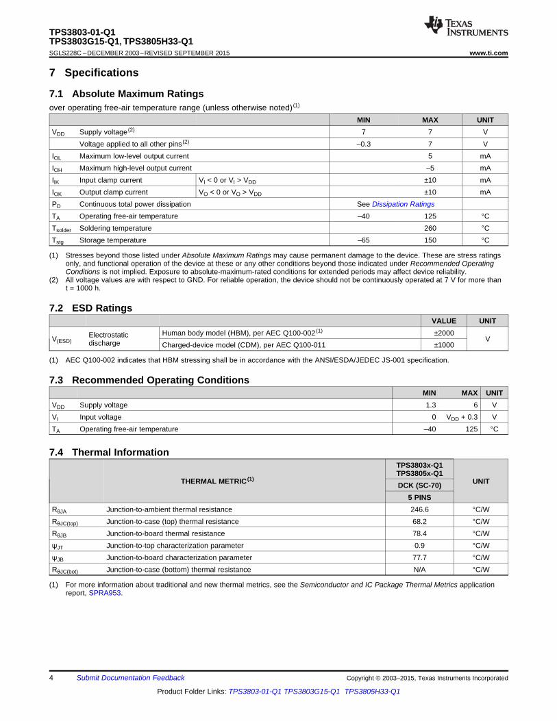
7 Specifications
7.1 Absolute Maximum Ratingsover operating free-air temperature range (unless otherwise noted) (1)
MIN MAX UNITVDD Supply voltage (2) 7 7 V
Voltage applied to all other pins (2) –0.3 7 VIOL Maximum low-level output current 5 mAIOH Maximum high-level output current –5 mAIIK Input clamp current VI < 0 or VI > VDD ±10 mAIOK Output clamp current VO < 0 or VO > VDD ±10 mAPD Continuous total power dissipation See Dissipation RatingsTA Operating free-air temperature –40 125 °CTsolder Soldering temperature 260 °CTstg Storage temperature –65 150 °C
(1) Stresses beyond those listed under Absolute Maximum Ratings may cause permanent damage to the device. These are stress ratingsonly, and functional operation of the device at these or any other conditions beyond those indicated under Recommended OperatingConditions is not implied. Exposure to absolute-maximum-rated conditions for extended periods may affect device reliability.
(2) All voltage values are with respect to GND. For reliable operation, the device should not be continuously operated at 7 V for more thant = 1000 h.
7.2 ESD RatingsVALUE UNIT
Human body model (HBM), per AEC Q100-002 (1) ±2000ElectrostaticV(ESD) Vdischarge Charged-device model (CDM), per AEC Q100-011 ±1000
(1) AEC Q100-002 indicates that HBM stressing shall be in accordance with the ANSI/ESDA/JEDEC JS-001 specification.
7.3 Recommended Operating ConditionsMIN MAX UNIT
VDD Supply voltage 1.3 6 VVI Input voltage 0 VDD + 0.3 VTA Operating free-air temperature –40 125 °C
7.4 Thermal InformationTPS3803x-Q1TPS3805x-Q1
THERMAL METRIC (1) UNITDCK (SC-70)5 PINS
RθJA Junction-to-ambient thermal resistance 246.6 °C/WRθJC(top) Junction-to-case (top) thermal resistance 68.2 °C/WRθJB Junction-to-board thermal resistance 78.4 °C/WψJT Junction-to-top characterization parameter 0.9 °C/WψJB Junction-to-board characterization parameter 77.7 °C/WRθJC(bot) Junction-to-case (bottom) thermal resistance N/A °C/W
(1) For more information about traditional and new thermal metrics, see the Semiconductor and IC Package Thermal Metrics applicationreport, SPRA953.
4 Submit Documentation Feedback Copyright © 2003–2015, Texas Instruments Incorporated
Product Folder Links: TPS3803-01-Q1 TPS3803G15-Q1 TPS3805H33-Q1

TPS3803-01-Q1TPS3803G15-Q1, TPS3805H33-Q1
www.ti.com SGLS228C –DECEMBER 2003–REVISED SEPTEMBER 2015
7.5 Electrical Characteristicsover operating free-air temperature range (unless otherwise noted)
PARAMETER TEST CONDITIONS MIN TYP MAX UNITVDD = 1.5 V, IOH = –0.5 mA
VOH High-level output voltage (TPS3805 only) VDD = 3.3 V, IOH = –1 mA 0.8 × VDD VVDD = 6 V, IOH = –1.5 mAVDD = 1.5 V, IOL = 1 mA
VOL Low-level output voltage VDD = 3.3 V, IOL = 2 mA 0.3 VVDD = 6 V, IOL = 3 mAVIT > 1.5 V, TA = 25°C 0.8
Power-up reset voltage (1) VVIT ≤ 1.5 V, TA = 25°C 1
SENSE 1.2 1.226 1.244Negative-going inputVIT TPS3803G15 1.379 1.4 1.421 Vthreshold voltage (2)
TPS3805H33 3.004 3.05 3.0961.2 V < VIT < 2.5 V 15
Vhys Hysteresis mV2.5 V < VIT < 3.5 V 30
II Input current SENSE –25 25 nAHigh-level outputIOH Open drain only VDD = VIT + 0.2 V, VOH = VDD 300 nAcurrent at RESET
TPS3803-01 2 4VDD = 3.3 V, Output unconnected
TPS3805, TPS3803G15 3 5IDD Supply current μA
TPS3803-01 2 4VDD = 6 V, Output unconnected
TPS3805, TPS3803G15 4 6CI Input capacitance VI = 0 V to VDD 1 pF
(1) The lowest supply voltage at which RESET (VOL(max) = 0.2 V, IOL = 50 μA) becomes active. tr(VDD) ≥ 15 μs/V.(2) To ensure the best stability of the threshold voltage, place a bypass capacitor (ceramic, 0.1-μF) near the supply terminals.
7.6 Timing RequirementsRL = 1 MΩ, CL = 50 pF, TA = –40°C to 125°C (unless otherwise noted)
MIN MAX UNITVDDtw Pulse duration VIH = 1.05 × VIT, VIL = 0.95 × VIT 5.5 μsSENSE
7.7 Switching CharacteristicsRL = 1 MΩ, CL = 50 pF, TA = –40°C to 125°C (unless otherwise noted)
PARAMETER TEST CONDITIONS MIN TYP MAX UNITVDD to RESET delayPropagation (delay) time,tPHL VIH = 1.05 × VIT, VIL = 0.95 × VIT 5 100 μshigh-to-low-level output SENSE to RESET delayVDD to RESET delay
Propagation (delay) time,tPLH VIH = 1.05 × VIT, VIL = 0.95 × VIT 5 100 μsSENSE to RESET delaylow-to-high-level outputμA
7.8 Dissipation RatingsPOWER RATING DERATING FACTOR POWER RATING POWER RATINGPACKAGE TA < 25°C ABOVE TA = 25°C TA = 70°C TA = 85°C
DCK 321 mW 2.6 mW/°C 206 mW 167 mW
Copyright © 2003–2015, Texas Instruments Incorporated Submit Documentation Feedback 5
Product Folder Links: TPS3803-01-Q1 TPS3803G15-Q1 TPS3805H33-Q1

VDD or SENSE
VIT + Vhys
VIT
0.8 V
RESET
= Undefined
TPS3803-01-Q1TPS3803G15-Q1, TPS3805H33-Q1SGLS228C –DECEMBER 2003–REVISED SEPTEMBER 2015 www.ti.com
Figure 1. Timing Requirements
6 Submit Documentation Feedback Copyright © 2003–2015, Texas Instruments Incorporated
Product Folder Links: TPS3803-01-Q1 TPS3803G15-Q1 TPS3805H33-Q1

0.7
0.6
0.5
0.4
0 2 4 6 8 10 12
0.8
0.9
1
14 16 18 20
85°C
0°C
25°C
-40 °C
VDD = 6 V
V(SENSE) = Low
0.3
0.2
0.1
0
(Expanded View)
I – Low-Level Output Current – mAOL
V– L
ow
-Level O
utp
utV
olt
ag
e –
VO
L
2
1.5
1
0.5
0 5 10 15 20 25 30
2.5
3
3.5
35 40 45 50
85°C
0°C
25°C
-40 °C
VDD = 6 V
V(SENSE) = Low
0
I – Low-Level Output Current – mAOL
V– L
ow
-Level O
utp
utV
olt
ag
e –
VO
L
1.00
0.80
0.60
0.40
0 1 2 3 4 5
1.20
1.40
1.60
I – Low-Level Output Current – mAOL
V– L
ow
-Level O
utp
utV
olt
ag
e –
VO
L
0.20
0
VDD = 1.5 V
V(SENSE) = Low
85°C
0°C
25°C
-40 °C
0.35
0.30
0.25
0.20
0 0.5 1 1.5 2 2.5 3
0.40
0.45
0.50
0.15
0.10
0.05
0
85°C
0°C
25°C
-40 °C
VDD = 1.5 V
V(SENSE) = Low
(Expanded View)
I – Low-Level Output Current – mAOL
V– L
ow
-Level O
utp
utV
olt
ag
e –
VO
L
3
2
1
00 0.5 1 1.5 2 2.5 3
4
5
6
3.5 4 4.5 5 5.5 6
SENSE = GND
RESET = Open
85°C
0°C
25°C
-40 °C
I– S
up
ply
Cu
rren
t – µ
AD
D
V – Supply Voltage – VDD
1.5
1
0.5
00 0.5 1 1.5 2 2.5 3
2
2.5
3
3.5 4 4.5 5 5.5 6
SENSE = GND
RESET = Open
85°C
0°C
-40 °C
25°C
I– S
up
ply
Cu
rren
t – µ
AD
D
V – Supply Voltage – VDD
TPS3803-01-Q1TPS3803G15-Q1, TPS3805H33-Q1
www.ti.com SGLS228C –DECEMBER 2003–REVISED SEPTEMBER 2015
7.9 Typical Characteristics
Figure 2. TPS3805H33-Q1 Supply Current vs Supply Voltage Figure 3. TPS3803-01-Q1 Supply Current vs Supply Voltage
Figure 4. Low-Level Output Voltage vs Low-Level Output Figure 5. Low-Level Output Voltage vs Low-Level OutputCurrent Current
Figure 6. Low-Level Output Voltage vs Low-Level Output Figure 7. Low-Level Output Voltage vs Low-Level OutputCurrent Current
Copyright © 2003–2015, Texas Instruments Incorporated Submit Documentation Feedback 7
Product Folder Links: TPS3803-01-Q1 TPS3803G15-Q1 TPS3805H33-Q1

1.0005
1.0000
0.9995
0.9990
-40 -20 0 20 40 60 80
1.0010
1.0015
1.0020
0.9985
0.9980
VDD = 6 V
RESET = 100 kW to VDD
T – Free-Air Temperature at SENSE – °CA
V– N
orm
alized
In
pu
tT
hre
sh
old
Vo
ltag
eV
(T)/
V(2
5°C
)IT
ITA
IT
5
4.5
4
3.5
-4 -3 -2 -1
5.5
6
30
85°C
0°C
25°C
-40 °C
VDD = 6 V
V(SENSE) = High
I – High-Level Output Current – mAOH
V– H
igh
-Level O
utp
utV
olt
ag
e –
VO
H
5.4
5.2
5
4.8
-14 -12 -10 -8 -6 -4
5.6
5.8
6
4.6-2 0
85°C
0°C
25°C
-40 °C
VDD = 6 V
V(SENSE) = High
(Expanded View)
I – High-Level Output Current – mAOH
V– H
igh
-Level O
utp
utV
olt
ag
e –
VO
H
2.75
2.25
2
1.75
-14 -12 -10 -8 -6 -4 -2
3
3.25
3.5
01.5
2.5
0°C
25°C
-40 °C
VDD = 3.3 V
V(SENSE) = High
85°C
I – High-Level Output Current – mAOH
V– H
igh
-Level O
utp
utV
olt
ag
e –
VO
H
3
2.9
2.8
2.7
-5 -4 -3 -2 -1 0
3.1
3.2
3.3
2.6
2.5
0°C
25°C
-40 °C
VDD = 3.3 V
V(SENSE) = High
85°C
(Expanded View)
I – High-Level Output Current – mAOH
V– H
igh
-Level O
utp
utV
olt
ag
e –
VO
H
TPS3803-01-Q1TPS3803G15-Q1, TPS3805H33-Q1SGLS228C –DECEMBER 2003–REVISED SEPTEMBER 2015 www.ti.com
Typical Characteristics (continued)
Figure 8. TPS3805H33-Q1 High-Level Output Voltage vs Figure 9. TPS3805H33-Q1 High-Level Output Voltage vsHigh-Level Output Current High-Level Output Current
Figure 10. TPS3805H33-Q1 High-Level Output Voltage vs Figure 11. TPS3805H33-Q1 High-Level Output Voltage vsHigh-Level Output Current High-Level Output Current
Figure 12. TPS3803-01-Q1 Normalized Input Threshold Voltage vs Free-Air Temperature At Sense
8 Submit Documentation Feedback Copyright © 2003–2015, Texas Instruments Incorporated
Product Folder Links: TPS3803-01-Q1 TPS3803G15-Q1 TPS3805H33-Q1

_
+
R1
R2
Reference
Voltage
of 1.215 V
RESETVDD
GND
_
+
Reference
Voltage
of 1.226 V
RESET
VDD
GND
SENSE
Device
Supply Voltage
_
+
_
+
R1
R2
VDD
GND
Reference
Voltage
of 1.226 V
SENSE
RESET
TPS3803G15-Q1 TPS3803-01-Q1
TPS3805H33-Q1
TPS3803-01-Q1TPS3803G15-Q1, TPS3805H33-Q1
www.ti.com SGLS228C –DECEMBER 2003–REVISED SEPTEMBER 2015
8 Detailed Description
8.1 OverviewThe TPS380x-Q1 devices are low-current supervisory circuits used to monitor system voltages above 1.226 V.The devices assert an active low RESET signal when VDD ,SENSE, or both voltages drop below a presetthreshold. The RESET output remains low until the VDD, SENSE, or both voltages return above their thresholds.The devices are also designed to be immune to short negative transients on the VDD and SENSE pins.
8.2 Functional Block Diagrams
8.3 Feature Description
8.3.1 VDD and SENSE MonitoringThe VDD and SENSE inputs provide a pin at which a system voltage can be monitored. If the voltage on this pindrops below VIT, RESET is asserted low. The comparator has a built-in hysteresis to ensure smooth RESETassertions and de-assertions. Refer to the Device Comparison Table to determine the VDD and SENSE voltagethresholds for each device. The adjustable version TPS3803-01-Q1 can be used to monitor any voltage rail downto 1.226 V using the circuit shown in Figure 13, where VIT' is the Vin threshold voltage.
Copyright © 2003–2015, Texas Instruments Incorporated Submit Documentation Feedback 9
Product Folder Links: TPS3803-01-Q1 TPS3803G15-Q1 TPS3805H33-Q1

7
6
5
4
0 0.1 0.2 0.3 0.4 0.5 0.6
8
9
10
0.7 0.8 0.9 1
3
2
1
0
VDD – Threshold Overdrive Voltage – V
t– M
inim
um
Pu
lse D
ura
tio
n a
tV
– µ
sw
DD
7
6
5
4
0 0.1 0.2 0.3 0.4 0.5 0.6
8
9
10
0.7 0.8 0.9 1
3
2
1
0
SENSE Threshold Overdrive Voltage – V–
t– M
inim
um
Pu
lse D
ura
tio
n a
t S
EN
SE
– µ
sw
VDD or SENSE
VIT
Overdrive
Voltage
Transient
Duration
VDD
TPS3803-01-Q1
SENSE
_____
RESET
GND
VIN
R1
R2
VIT[= (1 + R1/R2)*1.226
Reset
TPS3803-01-Q1TPS3803G15-Q1, TPS3805H33-Q1SGLS228C –DECEMBER 2003–REVISED SEPTEMBER 2015 www.ti.com
Feature Description (continued)
Figure 13. Using Adjustable Version
8.3.2 Transient ImmunityThe TPS380x-Q1 devices are immune to short negative transients on the VDD and SENSE pins. Sensitivity totransients is dependent on threshold overdrive as shown in Figure 15 and Figure 16. These graphs show theduration that the transient is below VIT compared to the magnitude of the voltage drop below VIT, called thethreshold overdrive voltage. Any combination of transient duration and overdrive voltage which lies above thecurves will result in RESET being asserted low. Any transient which lies below the curves will be ignored by thedevice.
Figure 14. Overdrive Voltage
Figure 15. Minimum Pulse Duration at VDD vs VDD Figure 16. Minimum Pulse Duration at Sense vs SenseThreshold Overdrive Voltage Threshold Overdrive Voltage
10 Submit Documentation Feedback Copyright © 2003–2015, Texas Instruments Incorporated
Product Folder Links: TPS3803-01-Q1 TPS3803G15-Q1 TPS3805H33-Q1

TPS3803-01-Q1TPS3803G15-Q1, TPS3805H33-Q1
www.ti.com SGLS228C –DECEMBER 2003–REVISED SEPTEMBER 2015
8.4 Device Functional ModesTPS3803-01-Q1 and TPS3803G15-Q1 monitor only one supply, which is SENSE and VDD respectively. Whenthat supply is above the VIT threshold, RESET will be high. Otherwise, RESET will be low. TPS3805H33-Q1monitors both VDD and SENSE. When both VDD and SENSE are above the VIT threshold, RESET will be high.Otherwise, RESET will be low.
Table 1. Function and TruthTable
TPS3803-01-Q1SENSE > VIT RESET
0 L1 H
Table 2. Function and TruthTable
TPS3803G15-Q1VDD > VIT RESET
0 L1 H
Table 3. Function and Truth TableTPS3805H33-Q1
VDD > VIT SENSE > VIT RESET0 0 L0 1 L1 0 L1 1 H
Copyright © 2003–2015, Texas Instruments Incorporated Submit Documentation Feedback 11
Product Folder Links: TPS3803-01-Q1 TPS3803G15-Q1 TPS3805H33-Q1

VDD
TPS3803G15-Q1
NC
_____
RESET
GND
VDD
RESET
1.5V
50 lQ
GND
Processor
TPS3803-01-Q1TPS3803G15-Q1, TPS3805H33-Q1SGLS228C –DECEMBER 2003–REVISED SEPTEMBER 2015 www.ti.com
9 Application and Implementation
NOTEInformation in the following applications sections is not part of the TI componentspecification, and TI does not warrant its accuracy or completeness. TI’s customers areresponsible for determining suitability of components for their purposes. Customers shouldvalidate and test their design implementation to confirm system functionality.
9.1 Application InformationThe TPS380x-Q1 voltage supervisor devices are designed to assert an active-low RESET signal when VDDand/or SENSE drop below a voltage threshold VIT. The RESET signal remains low until the voltages returnabove their respective thresholds. The TPS3803G15-Q1 and TPS3805H33-Q1 are fixed-voltage options, whilethe TPS3803-01-Q1 is adjustable and can be used to monitor any voltage above 1.226 V. The TPS3803G15-Q1and TPS3803-01-Q1 have an open-drain output, requiring an external pull-up on the RESET line.
9.2 Typical Applications
9.2.1 TPS3803G15-Q1
Figure 17. TPS3803G15 Typical Application
9.2.1.1 Design RequirementsWhen a single 1.5-V supply rail needs to be monitored, TPS3803G15-Q1 should be used. When a single voltagehigher than 1.226 V needs to be monitored, TPS3803-01-Q1 should be used. When a 3.3-V supply and secondsupply above 1.226 V needs to be monitored, TPS3805H33-Q1 should be used.
9.2.1.2 Detailed Design ProcedureTo monitor a single 1.5-V supply with TPS3803G15-Q1, connect the 1.5-V supply directly to VDD. The RESEToutput should be connected to the reset of the microcontroller with a pull-up resistor from the RESET output toVDD.
To monitor a single supply using TPS3803-01-Q1, connect the supply to VDD with a resistor divider to scale downthe voltage at the SENSE pin. The resistor values must be chosen to satisfy Equation 1:
VIT' = (1 + R1/R2) × 1.226
where• VIT’ is the VDD threshold voltage. (1)
For example, if TPS3803-01-Q1 should monitor a 2.5-V supply and the desired threshold voltage is 2.2 V, R1and R2 values could be 24 kΩ and 30- kΩ respectively. A 1-nf to 10-nF decoupling capacitor is recommended tobe placed close to the SENSE input.
12 Submit Documentation Feedback Copyright © 2003–2015, Texas Instruments Incorporated
Product Folder Links: TPS3803-01-Q1 TPS3803G15-Q1 TPS3805H33-Q1

VDD
_____
RESET
GND
VDD
TPS3803-01-Q1
SENSE
_____
RESET
GND
VIN
R1
R2
Processor
50 lQ
3
2
1
00 0.5 1 1.5 2 2.5 3
4
5
6
3.5 4 4.5 5 5.5 6
SENSE = GND
RESET = Open
85°C
0°C
25°C
-40 °C
I– S
up
ply
Cu
rren
t – µ
AD
D
V – Supply Voltage – VDD
1.5
1
0.5
00 0.5 1 1.5 2 2.5 3
2
2.5
3
3.5 4 4.5 5 5.5 6
SENSE = GND
RESET = Open
85°C
0°C
-40 °C
25°C
I– S
up
ply
Cu
rren
t – µ
AD
D
V – Supply Voltage – VDD
TPS3803-01-Q1TPS3803G15-Q1, TPS3805H33-Q1
www.ti.com SGLS228C –DECEMBER 2003–REVISED SEPTEMBER 2015
Typical Applications (continued)To monitor two supplies using TPS3805H33-Q1, connect the 3.3-V supply directly to VDD, and the second supplythrough a resistor divider to the SENSE pin. The SENSE pin should have a 1-nf to 10-nF decoupling capacitorclose to the pin.
9.2.1.3 Application Curves
Figure 18. TPS3805H33-Q1 Supply Current vs Supply Figure 19. TPS3803-01-Q1 Supply Current vs SupplyVoltage Voltage
9.2.2 TPS3803-01-Q1
Figure 20. TPS3803-01-Q1 Typical Application
9.2.2.1 Design RequirementsPlease refer to Design Requirements for this device's design requirements.
Copyright © 2003–2015, Texas Instruments Incorporated Submit Documentation Feedback 13
Product Folder Links: TPS3803-01-Q1 TPS3803G15-Q1 TPS3805H33-Q1

VDD
TPS3805H33-Q1
SENSE
_____
RESET
GND
VDD1
RESET
3.3V
GND
ProcessorR1
R2
VDD2
VDD2
TPS3803-01-Q1TPS3803G15-Q1, TPS3805H33-Q1SGLS228C –DECEMBER 2003–REVISED SEPTEMBER 2015 www.ti.com
Typical Applications (continued)9.2.3 TPS3805H33-Q1
Figure 21. TPS3805H33-Q1 Typical Application
9.2.3.1 Design RequirementsPlease refer to Design Requirements for this device's design requirements.
10 Power Supply RecommendationsThe TPS380x-Q1 devices are designed to operate from an input supply from 1.3 V to 6 V. TI recommends toplace a 0.1-µF capacitor near the VDD pin.
14 Submit Documentation Feedback Copyright © 2003–2015, Texas Instruments Incorporated
Product Folder Links: TPS3803-01-Q1 TPS3803G15-Q1 TPS3805H33-Q1

R1 R2
NC
GND
RESET
SENSE
VDD
CVDD
TPS3803-01-Q1C
R
Denotes GND Via
NC
GND
RESET
NC
VDD
CVDD
TPS3803G15-Q1
R
Denotes GND Via
TPS3803-01-Q1TPS3803G15-Q1, TPS3805H33-Q1
www.ti.com SGLS228C –DECEMBER 2003–REVISED SEPTEMBER 2015
11 Layout
11.1 Layout GuidelinesTI recommends to place the 0.1-µF decoupling capacitor close to the VDD pin. The VDD trace should be able tocarry 6 µA without a significant drop in voltage. Avoid a long trace from the SENSE pin to the resistor divider.
11.2 Layout Examples
Figure 22. TPS3803G15-Q1 Layout Example
Figure 23. TPS3803-01-Q1 Layout Example
Copyright © 2003–2015, Texas Instruments Incorporated Submit Documentation Feedback 15
Product Folder Links: TPS3803-01-Q1 TPS3803G15-Q1 TPS3805H33-Q1

R1
R2
NC
GND
RESET
SENSE
VDD
CVDD
TPS3805H33-Q1C
Denotes GND Via
TPS3803-01-Q1TPS3803G15-Q1, TPS3805H33-Q1SGLS228C –DECEMBER 2003–REVISED SEPTEMBER 2015 www.ti.com
Layout Examples (continued)
Figure 24. TPS3805H33-Q1 Layout Example
16 Submit Documentation Feedback Copyright © 2003–2015, Texas Instruments Incorporated
Product Folder Links: TPS3803-01-Q1 TPS3803G15-Q1 TPS3805H33-Q1

TPS380 3 G 15 DCK R
Reel
Package
Nominal Supply Voltage
Nominal Threshold Voltage
FunctionalityFamily
Q
Temperature Designator
Q1
Customer Suffix
TPS3803-01-Q1TPS3803G15-Q1, TPS3805H33-Q1
www.ti.com SGLS228C –DECEMBER 2003–REVISED SEPTEMBER 2015
12 Device and Documentation Support
12.1 Device Support
12.1.1 Device Nomenclature
12.2 Related LinksThe table below lists quick access links. Categories include technical documents, support and communityresources, tools and software, and quick access to sample or buy.
Table 4. Related LinksTECHNICAL TOOLS & SUPPORT &PARTS PRODUCT FOLDER SAMPLE & BUY DOCUMENTS SOFTWARE COMMUNITY
TPS3803-01-Q1 Click here Click here Click here Click here Click hereTPS3803G15-Q1 Click here Click here Click here Click here Click hereTPS3805H33-Q1 Click here Click here Click here Click here Click here
12.3 Community ResourcesThe following links connect to TI community resources. Linked contents are provided "AS IS" by the respectivecontributors. They do not constitute TI specifications and do not necessarily reflect TI's views; see TI's Terms ofUse.
TI E2E™ Online Community TI's Engineer-to-Engineer (E2E) Community. Created to foster collaborationamong engineers. At e2e.ti.com, you can ask questions, share knowledge, explore ideas and helpsolve problems with fellow engineers.
Design Support TI's Design Support Quickly find helpful E2E forums along with design support tools andcontact information for technical support.
12.4 TrademarksE2E is a trademark of Texas Instruments.All other trademarks are the property of their respective owners.
12.5 Electrostatic Discharge CautionThese devices have limited built-in ESD protection. The leads should be shorted together or the device placed in conductive foamduring storage or handling to prevent electrostatic damage to the MOS gates.
12.6 GlossarySLYZ022 — TI Glossary.
This glossary lists and explains terms, acronyms, and definitions.
Copyright © 2003–2015, Texas Instruments Incorporated Submit Documentation Feedback 17
Product Folder Links: TPS3803-01-Q1 TPS3803G15-Q1 TPS3805H33-Q1

TPS3803-01-Q1TPS3803G15-Q1, TPS3805H33-Q1SGLS228C –DECEMBER 2003–REVISED SEPTEMBER 2015 www.ti.com
13 Mechanical, Packaging, and Orderable InformationThe following pages include mechanical, packaging, and orderable information. This information is the mostcurrent data available for the designated devices. This data is subject to change without notice and revision ofthis document. For browser-based versions of this data sheet, refer to the left-hand navigation.
18 Submit Documentation Feedback Copyright © 2003–2015, Texas Instruments Incorporated
Product Folder Links: TPS3803-01-Q1 TPS3803G15-Q1 TPS3805H33-Q1

PACKAGE OPTION ADDENDUM
www.ti.com 22-Dec-2016
Addendum-Page 1
PACKAGING INFORMATION
Orderable Device Status(1)
Package Type PackageDrawing
Pins PackageQty
Eco Plan(2)
Lead/Ball Finish(6)
MSL Peak Temp(3)
Op Temp (°C) Device Marking(4/5)
Samples
2T03-01QDCKRG4Q1 ACTIVE SC70 DCK 5 3000 Green (RoHS& no Sb/Br)
CU NIPDAUAG Level-1-260C-UNLIM -40 to 125 AWJ
2T03G15QDCKRG4Q ACTIVE SC70 DCK 5 3000 Green (RoHS& no Sb/Br)
CU NIPDAUAG Level-1-260C-UNLIM -40 to 125 AXU
2T05H33QDCKRG4Q ACTIVE SC70 DCK 5 3000 Green (RoHS& no Sb/Br)
CU NIPDAU |CU NIPDAUAG
Level-1-260C-UNLIM -40 to 125 AWZ
TPS3803-01QDCKRQ1 ACTIVE SC70 DCK 5 3000 Green (RoHS& no Sb/Br)
CU NIPDAUAG Level-1-260C-UNLIM -40 to 125 AWJ
TPS3803G15QDCKRQ1 ACTIVE SC70 DCK 5 3000 Green (RoHS& no Sb/Br)
CU NIPDAU |CU NIPDAUAG
Level-1-260C-UNLIM -40 to 125 AXU
TPS3805H33QDCKRQ1 ACTIVE SC70 DCK 5 3000 Green (RoHS& no Sb/Br)
CU NIPDAU |CU NIPDAUAG
Level-1-260C-UNLIM -40 to 125 AWZ
(1) The marketing status values are defined as follows:ACTIVE: Product device recommended for new designs.LIFEBUY: TI has announced that the device will be discontinued, and a lifetime-buy period is in effect.NRND: Not recommended for new designs. Device is in production to support existing customers, but TI does not recommend using this part in a new design.PREVIEW: Device has been announced but is not in production. Samples may or may not be available.OBSOLETE: TI has discontinued the production of the device.
(2) Eco Plan - The planned eco-friendly classification: Pb-Free (RoHS), Pb-Free (RoHS Exempt), or Green (RoHS & no Sb/Br) - please check http://www.ti.com/productcontent for the latest availabilityinformation and additional product content details.TBD: The Pb-Free/Green conversion plan has not been defined.Pb-Free (RoHS): TI's terms "Lead-Free" or "Pb-Free" mean semiconductor products that are compatible with the current RoHS requirements for all 6 substances, including the requirement thatlead not exceed 0.1% by weight in homogeneous materials. Where designed to be soldered at high temperatures, TI Pb-Free products are suitable for use in specified lead-free processes.Pb-Free (RoHS Exempt): This component has a RoHS exemption for either 1) lead-based flip-chip solder bumps used between the die and package, or 2) lead-based die adhesive used betweenthe die and leadframe. The component is otherwise considered Pb-Free (RoHS compatible) as defined above.Green (RoHS & no Sb/Br): TI defines "Green" to mean Pb-Free (RoHS compatible), and free of Bromine (Br) and Antimony (Sb) based flame retardants (Br or Sb do not exceed 0.1% by weightin homogeneous material)
(3) MSL, Peak Temp. - The Moisture Sensitivity Level rating according to the JEDEC industry standard classifications, and peak solder temperature.
(4) There may be additional marking, which relates to the logo, the lot trace code information, or the environmental category on the device.
(5) Multiple Device Markings will be inside parentheses. Only one Device Marking contained in parentheses and separated by a "~" will appear on a device. If a line is indented then it is a continuationof the previous line and the two combined represent the entire Device Marking for that device.

PACKAGE OPTION ADDENDUM
www.ti.com 22-Dec-2016
Addendum-Page 2
(6) Lead/Ball Finish - Orderable Devices may have multiple material finish options. Finish options are separated by a vertical ruled line. Lead/Ball Finish values may wrap to two lines if the finishvalue exceeds the maximum column width.
Important Information and Disclaimer:The information provided on this page represents TI's knowledge and belief as of the date that it is provided. TI bases its knowledge and belief on informationprovided by third parties, and makes no representation or warranty as to the accuracy of such information. Efforts are underway to better integrate information from third parties. TI has taken andcontinues to take reasonable steps to provide representative and accurate information but may not have conducted destructive testing or chemical analysis on incoming materials and chemicals.TI and TI suppliers consider certain information to be proprietary, and thus CAS numbers and other limited information may not be available for release.
In no event shall TI's liability arising out of such information exceed the total purchase price of the TI part(s) at issue in this document sold by TI to Customer on an annual basis.
OTHER QUALIFIED VERSIONS OF TPS3803-01-Q1, TPS3803-Q1, TPS3805H33-Q1 :
• Catalog: TPS3803-01, TPS3803, TPS3805H33
• Enhanced Product: TPS3803-01-EP, TPS3803-EP, TPS3805H33-EP
NOTE: Qualified Version Definitions:
• Catalog - TI's standard catalog product
• Enhanced Product - Supports Defense, Aerospace and Medical Applications

TAPE AND REEL INFORMATION
*All dimensions are nominal
Device PackageType
PackageDrawing
Pins SPQ ReelDiameter
(mm)
ReelWidth
W1 (mm)
A0(mm)
B0(mm)
K0(mm)
P1(mm)
W(mm)
Pin1Quadrant
TPS3803G15QDCKRQ1 SC70 DCK 5 3000 180.0 8.4 2.47 2.3 1.25 4.0 8.0 Q3
PACKAGE MATERIALS INFORMATION
www.ti.com 8-Feb-2018
Pack Materials-Page 1

*All dimensions are nominal
Device Package Type Package Drawing Pins SPQ Length (mm) Width (mm) Height (mm)
TPS3803G15QDCKRQ1 SC70 DCK 5 3000 183.0 183.0 20.0
PACKAGE MATERIALS INFORMATION
www.ti.com 8-Feb-2018
Pack Materials-Page 2


IMPORTANT NOTICE
Texas Instruments Incorporated (TI) reserves the right to make corrections, enhancements, improvements and other changes to itssemiconductor products and services per JESD46, latest issue, and to discontinue any product or service per JESD48, latest issue. Buyersshould obtain the latest relevant information before placing orders and should verify that such information is current and complete.TI’s published terms of sale for semiconductor products (http://www.ti.com/sc/docs/stdterms.htm) apply to the sale of packaged integratedcircuit products that TI has qualified and released to market. Additional terms may apply to the use or sale of other types of TI products andservices.Reproduction of significant portions of TI information in TI data sheets is permissible only if reproduction is without alteration and isaccompanied by all associated warranties, conditions, limitations, and notices. TI is not responsible or liable for such reproduceddocumentation. Information of third parties may be subject to additional restrictions. Resale of TI products or services with statementsdifferent from or beyond the parameters stated by TI for that product or service voids all express and any implied warranties for theassociated TI product or service and is an unfair and deceptive business practice. TI is not responsible or liable for any such statements.Buyers and others who are developing systems that incorporate TI products (collectively, “Designers”) understand and agree that Designersremain responsible for using their independent analysis, evaluation and judgment in designing their applications and that Designers havefull and exclusive responsibility to assure the safety of Designers' applications and compliance of their applications (and of all TI productsused in or for Designers’ applications) with all applicable regulations, laws and other applicable requirements. Designer represents that, withrespect to their applications, Designer has all the necessary expertise to create and implement safeguards that (1) anticipate dangerousconsequences of failures, (2) monitor failures and their consequences, and (3) lessen the likelihood of failures that might cause harm andtake appropriate actions. Designer agrees that prior to using or distributing any applications that include TI products, Designer willthoroughly test such applications and the functionality of such TI products as used in such applications.TI’s provision of technical, application or other design advice, quality characterization, reliability data or other services or information,including, but not limited to, reference designs and materials relating to evaluation modules, (collectively, “TI Resources”) are intended toassist designers who are developing applications that incorporate TI products; by downloading, accessing or using TI Resources in anyway, Designer (individually or, if Designer is acting on behalf of a company, Designer’s company) agrees to use any particular TI Resourcesolely for this purpose and subject to the terms of this Notice.TI’s provision of TI Resources does not expand or otherwise alter TI’s applicable published warranties or warranty disclaimers for TIproducts, and no additional obligations or liabilities arise from TI providing such TI Resources. TI reserves the right to make corrections,enhancements, improvements and other changes to its TI Resources. TI has not conducted any testing other than that specificallydescribed in the published documentation for a particular TI Resource.Designer is authorized to use, copy and modify any individual TI Resource only in connection with the development of applications thatinclude the TI product(s) identified in such TI Resource. NO OTHER LICENSE, EXPRESS OR IMPLIED, BY ESTOPPEL OR OTHERWISETO ANY OTHER TI INTELLECTUAL PROPERTY RIGHT, AND NO LICENSE TO ANY TECHNOLOGY OR INTELLECTUAL PROPERTYRIGHT OF TI OR ANY THIRD PARTY IS GRANTED HEREIN, including but not limited to any patent right, copyright, mask work right, orother intellectual property right relating to any combination, machine, or process in which TI products or services are used. Informationregarding or referencing third-party products or services does not constitute a license to use such products or services, or a warranty orendorsement thereof. Use of TI Resources may require a license from a third party under the patents or other intellectual property of thethird party, or a license from TI under the patents or other intellectual property of TI.TI RESOURCES ARE PROVIDED “AS IS” AND WITH ALL FAULTS. TI DISCLAIMS ALL OTHER WARRANTIES ORREPRESENTATIONS, EXPRESS OR IMPLIED, REGARDING RESOURCES OR USE THEREOF, INCLUDING BUT NOT LIMITED TOACCURACY OR COMPLETENESS, TITLE, ANY EPIDEMIC FAILURE WARRANTY AND ANY IMPLIED WARRANTIES OFMERCHANTABILITY, FITNESS FOR A PARTICULAR PURPOSE, AND NON-INFRINGEMENT OF ANY THIRD PARTY INTELLECTUALPROPERTY RIGHTS. TI SHALL NOT BE LIABLE FOR AND SHALL NOT DEFEND OR INDEMNIFY DESIGNER AGAINST ANY CLAIM,INCLUDING BUT NOT LIMITED TO ANY INFRINGEMENT CLAIM THAT RELATES TO OR IS BASED ON ANY COMBINATION OFPRODUCTS EVEN IF DESCRIBED IN TI RESOURCES OR OTHERWISE. IN NO EVENT SHALL TI BE LIABLE FOR ANY ACTUAL,DIRECT, SPECIAL, COLLATERAL, INDIRECT, PUNITIVE, INCIDENTAL, CONSEQUENTIAL OR EXEMPLARY DAMAGES INCONNECTION WITH OR ARISING OUT OF TI RESOURCES OR USE THEREOF, AND REGARDLESS OF WHETHER TI HAS BEENADVISED OF THE POSSIBILITY OF SUCH DAMAGES.Unless TI has explicitly designated an individual product as meeting the requirements of a particular industry standard (e.g., ISO/TS 16949and ISO 26262), TI is not responsible for any failure to meet such industry standard requirements.Where TI specifically promotes products as facilitating functional safety or as compliant with industry functional safety standards, suchproducts are intended to help enable customers to design and create their own applications that meet applicable functional safety standardsand requirements. Using products in an application does not by itself establish any safety features in the application. Designers mustensure compliance with safety-related requirements and standards applicable to their applications. Designer may not use any TI products inlife-critical medical equipment unless authorized officers of the parties have executed a special contract specifically governing such use.Life-critical medical equipment is medical equipment where failure of such equipment would cause serious bodily injury or death (e.g., lifesupport, pacemakers, defibrillators, heart pumps, neurostimulators, and implantables). Such equipment includes, without limitation, allmedical devices identified by the U.S. Food and Drug Administration as Class III devices and equivalent classifications outside the U.S.TI may expressly designate certain products as completing a particular qualification (e.g., Q100, Military Grade, or Enhanced Product).Designers agree that it has the necessary expertise to select the product with the appropriate qualification designation for their applicationsand that proper product selection is at Designers’ own risk. Designers are solely responsible for compliance with all legal and regulatoryrequirements in connection with such selection.Designer will fully indemnify TI and its representatives against any damages, costs, losses, and/or liabilities arising out of Designer’s non-compliance with the terms and provisions of this Notice.
Mailing Address: Texas Instruments, Post Office Box 655303, Dallas, Texas 75265Copyright © 2018, Texas Instruments Incorporated