sending location-based keys using visible light communication1058125/fulltext01.pdf · sending...
TRANSCRIPT
IT 16 041
Examensarbete 30 hpJune 2016
Sending Location-Based Keys Using Visible Light Communication
Estuardo Rene Garcia Velasquez
Institutionen för informationsteknologiDepartment of Information Technology

ii

Teknisk- naturvetenskaplig fakultet UTH-enheten Besöksadress: Ångströmlaboratoriet Lägerhyddsvägen 1 Hus 4, Plan 0 Postadress: Box 536 751 21 Uppsala Telefon: 018 – 471 30 03 Telefax: 018 – 471 30 00 Hemsida: http://www.teknat.uu.se/student
Abstract
Sending Location-Based Keys Using Visible LightCommunication
Estuardo Rene Garcia Velasquez
In this thesis we present a Security Application based on Visible Light Communication(VLC). As VLC continues to develop, the need to protect valuable informationtransmitted using this type of communication is also growing. We aim to protect thisvaluable information by proposing a security application in which the data is encryptedin a multiple-light system and only recoverable in specific locations of a movingpattern within specific time. We use the Shamir Secret Sharing algorithm as basis forthe encryption combined with additional algorithms to provide a more securetransmission. The application is formed by the Physical Layer which is in charge ofproviding the optimal configuration for transmission and the Application Layer inwhich we implement the encryption and decryption algorithms for the application.The Physical Layer is formed by a group of LED bulbs controlled by an FPGA usingPWM to represent the information. We propose a scheduling algorithm in which thelights are scheduled in a bit-by-bit manner. The reception part is formed by theOPT101 optical receiver connected to the ultra-low power TS881 comparator. Asecond FPGA is in charge of demodulating the signals from the comparator bymeasuring the period of each signal to detect the corresponding bit. To evaluate theSecurity Application and to find best configurations for the Physical Layer we performa series of experiments in which we modify the responsivity of the receiver underdifferent scenarios including variations of transmission angles, data rates, and heights.The results show that adjusting the sensitivity of the receiver plays a major role in theapplication as we shows different types of configurations to adjust the areas in whichthe information can be received.
IT 16 041Examinator: Arnold Neville PearsÄmnesgranskare: Thiemo VoigtHandledare: Christian Rohner

iv

v
ACKNOWLEDGEMENT
This project could not have been possible without the support from many people over the last semester. I would like to thank everyone from the Uppsala Networked Objects (UNO) group for letting me be part of the team. Special thanks to Thiemo Voigt for giving his time in the revision of the project and report. My sincere gratitude to Christian Rohner for allowing me to work under his supervision and for his guidance throughout this project. Thanks to Ambuj Varshney for sharing his ideas and also for his motivation during these last months which made me constantly increase my desire to strive for excellence. Thanks to Kasun Hewage for his guidance and valuable feedback. I would also like to thank Abdalah Hilmia for allowing me to continue his work. Finally, thanks to all my friends and family who stood by my side during the whole master program and during the completion of this project.

vi
CONTENTS
Chapter 1 INTRODUCTION ......................................................................................................................... 1
1.1 Motivation ..................................................................................................................................... 1
1.2 Problem Statement ....................................................................................................................... 2
1.3 Goals ............................................................................................................................................. 2
1.3.1 Application Layer .................................................................................................................. 2
1.3.2 Physical Layer ........................................................................................................................ 2
1.4 Methodology ................................................................................................................................. 3
1.5 Results ........................................................................................................................................... 3
1.6 Thesis Structure ............................................................................................................................ 3
Chapter 2 RELATED WORK ......................................................................................................................... 5
Chapter 3 BACKGROUND ........................................................................................................................... 7
3.1 Types of Modulation ..................................................................................................................... 7
3.1.1 OOK ....................................................................................................................................... 7
3.1.2 BFSK ....................................................................................................................................... 7
3.1.3 PWM...................................................................................................................................... 8
3.2 OPT101 Optical Receiver ............................................................................................................... 8
3.2.1 P-‐N Junction .......................................................................................................................... 8
3.2.2 Photodiode ............................................................................................................................ 8
3.2.3 Transimpedance amplifier .................................................................................................... 9
3.2.4 All-‐in-‐One OPT101 ................................................................................................................. 9
3.2.5 Feedback Network and Responsivity .................................................................................... 9
3.2.6 Rise Time ............................................................................................................................. 10
3.3 TS881 Comparator ...................................................................................................................... 10
3.4 Data Slicer ................................................................................................................................... 11
3.5 Shamir Secret Sharing Algorithm ................................................................................................ 13
3.6 Field Programmable Gate Arrays ................................................................................................ 14
3.7 Linear Feedback Shift Registers .................................................................................................. 14
3.8 Beam Spread ............................................................................................................................... 15
Chapter 4 DESGIN CONSIDERATIONS ...................................................................................................... 17
4.1 Modulations ................................................................................................................................ 17
4.1.1 On-‐Off Keying ...................................................................................................................... 17
4.1.2 BFSK ..................................................................................................................................... 17

vii
Chapter 5 DESIGN AND IMPLEMENTATION OF PHYSICAL LAYER ............................................................ 21
5.1 Frame Structure .......................................................................................................................... 21
5.2 Sender Subsystem ....................................................................................................................... 22
5.2.1 Driving the LEDs .................................................................................................................. 22
5.2.2 Pulse Width Modulation ..................................................................................................... 23
5.2.3 Scheduling the LEDs ............................................................................................................ 23
5.2.4 Encoding Algorithm ............................................................................................................. 24
5.3 Receiver Subsystem .................................................................................................................... 24
5.3.1 OPT101 Feedback Network ................................................................................................. 25
5.3.2 Data Slicer ........................................................................................................................... 25
5.3.3 Reception Algorithm ........................................................................................................... 26
Chapter 6 SECURITY APPLICATION .......................................................................................................... 29
6.1 Application Overview .................................................................................................................. 29
6.2 Encryption of the Secret ............................................................................................................. 30
6.2.1 Security Level # 1: Polynomial ............................................................................................ 30
6.2.2 Security Level # 2: Path Dependency .................................................................................. 31
6.2.3 Security Level # 3: Intersecting Areas ................................................................................. 31
6.2.4 Security Level # 4: Time Dependency ................................................................................. 31
6.2.5 Security Level # 5: XOR Every Frame ................................................................................... 32
6.2.6 Combined Security Levels ................................................................................................... 33
6.3 Decryption of the Secret ............................................................................................................. 34
6.3.1 XOR Encryption and Shares ................................................................................................. 34
6.3.2 Time Dependency ............................................................................................................... 34
6.3.3 Path Dependency and Reconstruction of Polynomial ........................................................ 34
Chapter 7 EVALUATION ........................................................................................................................... 37
7.1 Receiver Circuit ........................................................................................................................... 37
7.2 Bit Error Rate ............................................................................................................................... 38
7.2.1 No background light ............................................................................................................ 38
7.2.2 Background light ................................................................................................................. 39
7.3 Causes of Errors .......................................................................................................................... 40
7.3.1 No background light ............................................................................................................ 40
7.3.2 Background Light................................................................................................................. 41
7.4 Impact of Data Slicer ................................................................................................................... 42
7.4.1 ...................................................................................... 42

viii
7.4.2 ............................................................................... 43
7.4.3 qual to 25% duty cycle using PWM ................................................................................ 44
7.4.4 .............................................................................. 45
7.5 Photodiode .................................................................................................................................. 46
7.5.1 Saturation ............................................................................................................................ 46
7.5.2 Responsivity Single Source without Background Light .................................................... 47
7.5.3 Responsivity Single Light with background Light ............................................................. 49
7.5.4 Responsivity Multiple Lights ............................................................................................ 50
7.6 Flickering ..................................................................................................................................... 50
7.7 Security Application .................................................................................................................... 51
Chapter 8 CONCLUSION AND FUTURE WORK ......................................................................................... 53
8.1 Physical Layer .............................................................................................................................. 53
8.2 Application Layer ........................................................................................................................ 54
APPENDIX A VHDL Encoding Algorithm ................................................................................................... 55
APPENDIX B VHDL Reception Algorithm .................................................................................................. 59
REFERENCES ................................................................................................................................................ 63

ix
LIST OF FIGURES Figure 1. Security application for multiple lights .......................................................................................... 1 Figure 2. On-‐Off Keying ................................................................................................................................. 7 Figure 3. Binary Frequency Shift Keying ....................................................................................................... 8 Figure 4. Pulse Width Modulation ................................................................................................................ 8 Figure 5. Internal feedback network response of OPT101 ......................................................................... 10 Figure 6. TS881 Comparator ....................................................................................................................... 10 Figure 7. Inputs to the op-‐amp ................................................................................................................... 10 Figure 8. Comparator operation ................................................................................................................. 11 Figure 9. Comparator with Fixed reference voltage ................................................................................... 11 Figure 10. Data Slicer circuit ....................................................................................................................... 12 Figure 11. Charging time of capacitor ......................................................................................................... 12 Figure 12. Data slicer as averaging circuit ................................................................................................... 13 Figure 13. LFSR using shift registers ............................................................................................................ 15 Figure 14. Increased ON signal length with OOK ........................................................................................ 17 Figure 15. Dominant frequency in BFSK ..................................................................................................... 18 Figure 16. Single signals for 10 string .......................................................................................................... 18 Figure 17. Duty cycle increased on both, 1 and 0, signals with BFSK produced by having background light .................................................................................................................................................................... 18 Figure 18. Duty cycle decreased on both, 1 and 0, signals with BFSK produced by removing background light ............................................................................................................................................................. 18 Figure 19. Security weakness from BFSK .................................................................................................... 19 Figure 20. System diagram .......................................................................................................................... 21
...................................................................................... 22 Figure 22. Ledsaver 12 V, 38°, 320 lm ......................................................................................................... 22 Figure 23. Circuit Schematic for LED driver ................................................................................................ 23 Figure 24. Binary string using PWM, 25% (0) and 75% (1) duty cycle ........................................................ 23 Figure 25. Bit-‐by-‐bit Scheduling of 3 lights ................................................................................................. 24 Figure 26. External Feedback for OPT101 ................................................................................................... 25 Figure 27. Data Slicer configuration for comparator .................................................................................. 26 Figure 28. Testbed for the Security Application ......................................................................................... 29 Figure 29. Example of a Secret .................................................................................................................... 30 Figure 30. Share distributed in two lights ................................................................................................... 31 Figure 31. Shares available during an epoch. ............................................................................................. 32 Figure 32. Combined Security Levels .......................................................................................................... 33 Figure 33. Output signal at 1 Kbps for large time constant ........................................................................ 38 Figure 34. Output signal at 15 Kbps for large time constant ...................................................................... 38 Figure 35. BER without background light.................................................................................................... 39 Figure 36. BER with background light ......................................................................................................... 40 Figure 37. Circuit of the comparator........................................................................................................... 40
ckground light. ................................................ 41 Figure 39. 15 Kbps at 25cm close to saturation region .............................................................................. 41 Figure 40. 20 Kbps at 25cm close to saturation region .............................................................................. 41
x
Figure 41. Noise produced by background light at 250 cm and 15 Kbps.................................................... 42 ............................................ 42
n using OOK ........................................................................................ 43 .......................................................................................... 43
Figure 45. False positives from data slicer .................................................................................................. 44 ........................................................................................................... 45
ler than bit duration using PWM ..................................................................................... 46 Figure 48. Photodiode driven by 3.3 V........................................................................................................ 47 Figure 49. Photodiode driven by 6 V ........................................................................................................... 47
.............................................................................. 48 Figure 51. High (a) vs. Low (b) gain at 45° ................................................................................................... 48 Figure 52. High (a) vs. Low (b) gain at 35° ................................................................................................... 48 Figure 53. High (a) vs. Low (b) gain at 25° ................................................................................................... 49 Figure 54. High (a) vs. Low (b) gain at 15° ................................................................................................... 49 Figure 55. High (a) vs. Low (b) gain at 0° ..................................................................................................... 49 Figure 56. Reception area at 0° with background light Low gain ............................................................ 50 Figure 57. Mirror of High gain at 0° ............................................................................................................ 50 Figure 58. Mirror of Low gain at 25° ........................................................................................................... 50 Figure 59. Top Level Schematic of the Encoding Algorithm ....................................................................... 55 Figure 60. FSM of Encoding Algorithm ....................................................................................................... 57 Figure 61. Top-‐Level Schematic of Receiver Algorithm .............................................................................. 59

xi
LIST OF TABLES Table 1. Time constant based on signal duration ....................................................................................... 26 Table 2. Polynomial for each byte in the Secret ......................................................................................... 31 Table 3. Points for each byte in the Secret ................................................................................................. 31 Table 4. Illuminance in lx at different distances, no background light. ...................................................... 39 Table 5. Illuminance in lx at different distances, background light ............................................................ 39 Table 6. Responsivity and Bandwith configurations ................................................................................... 47

xii
ABBREVIATIONS AND ACRONYMS ADC Analog to Digital Comparator BER Bit Error Rate FPGA Field Programmable Gate Array LED Light Emitting Diode LFSR Linear Feedback Shift Register LSB Least Significant Bit MCU -‐ Microcontroller Unit MSB Most Significant Bit VLC Visible Light Communication RF Radio Frequency (signals)
Page | 1
Chapter 1 INTRODUCTION
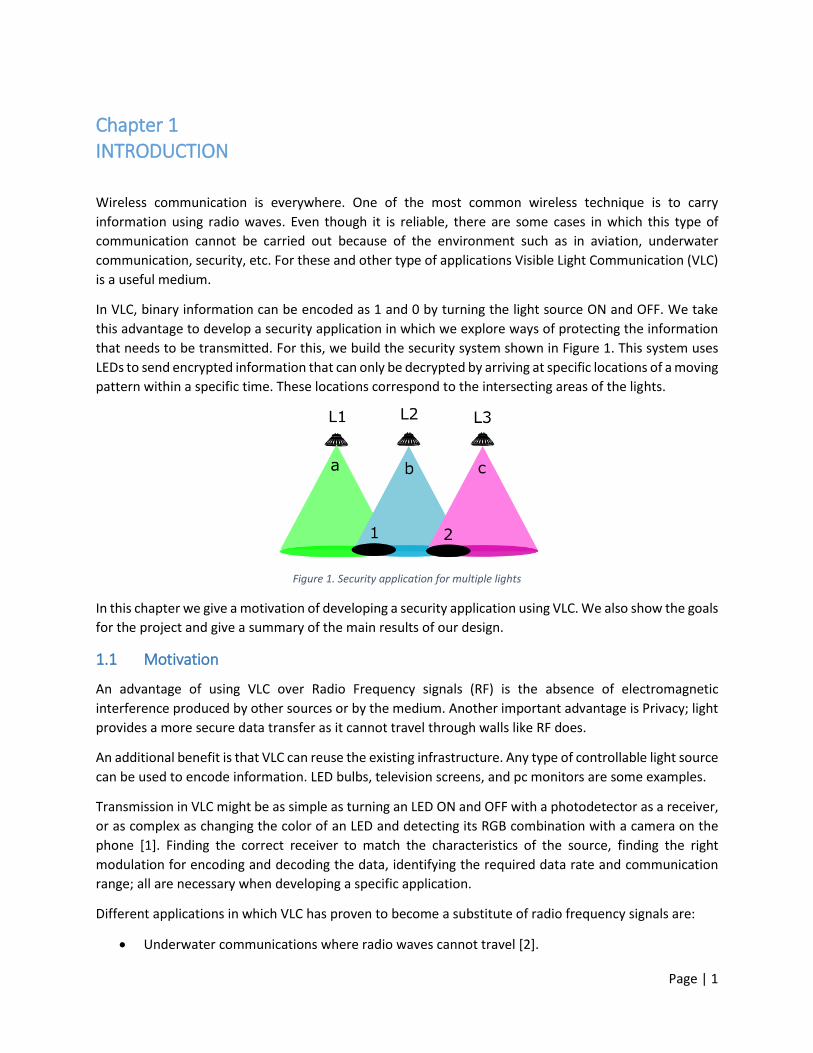
Wireless communication is everywhere. One of the most common wireless technique is to carry information using radio waves. Even though it is reliable, there are some cases in which this type of communication cannot be carried out because of the environment such as in aviation, underwater communication, security, etc. For these and other type of applications Visible Light Communication (VLC) is a useful medium.
In VLC, binary information can be encoded as 1 and 0 by turning the light source ON and OFF. We take this advantage to develop a security application in which we explore ways of protecting the information that needs to be transmitted. For this, we build the security system shown in Figure 1. This system uses LEDs to send encrypted information that can only be decrypted by arriving at specific locations of a moving pattern within a specific time. These locations correspond to the intersecting areas of the lights.
Figure 1. Security application for multiple lights
In this chapter we give a motivation of developing a security application using VLC. We also show the goals for the project and give a summary of the main results of our design.
1.1 Motivation
An advantage of using VLC over Radio Frequency signals (RF) is the absence of electromagnetic interference produced by other sources or by the medium. Another important advantage is Privacy; light provides a more secure data transfer as it cannot travel through walls like RF does.
An additional benefit is that VLC can reuse the existing infrastructure. Any type of controllable light source can be used to encode information. LED bulbs, television screens, and pc monitors are some examples.
Transmission in VLC might be as simple as turning an LED ON and OFF with a photodetector as a receiver, or as complex as changing the color of an LED and detecting its RGB combination with a camera on the phone [1]. Finding the correct receiver to match the characteristics of the source, finding the right modulation for encoding and decoding the data, identifying the required data rate and communication range; all are necessary when developing a specific application.
Different applications in which VLC has proven to become a substitute of radio frequency signals are:
Underwater communications where radio waves cannot travel [2].

Page | 2
Aviation, Hospitals, and Healthcare in which electromagnetic signals must be removed when operating other devices such as planes or MRI machines [3].
Smart lighting in order to provide the network for interaction and control of devices to reduce energy consumption [4].
Security in which communication can be limited to specific location and closed areas [5].
Because of the high efficiency, low-‐price, and long-‐life expectancy, Light Emitting Diode (LED) lamps have gained dominance in applications such as walkway lights, traffic signals, automotive industry, room lighting, etc. [6]. It is not only the wide use of LEDs that make them convenient for VLC, but also the high speed in which they can be turned ON and OFF and still be undetectable for the human eye.
The increasing use of VLC and the advantages of LED bulbs provide major motivations for developing a Security application with LED as data transmitters in this project.
1.2 Problem Statement
As VLC continues to develop, stable and secure links are still to be improved. Some of the already implemented multiple-‐light VLC systems are low-‐cost and low-‐power consumption but also have low communication range and low data rates [5], [7], [8].
Most of these systems fall behind as they are not low-‐power system or do not achieve high data rates and communication range.
The main focus is to build a system that combines high data rates, low power consumption, and long communication range into a working system intended for security.
1.3 Goals
The goals of the thesis are defined in two layers: the Application Layer which constitutes the implementation of a Security application, and the Physical Layer which define the physical requirements of the application.
1.3.1 Application Layer
The goal of the Application Layer is to design and implement a Security system where,
1. Lights are placed in a straight line forming two different intersections. 2. Information is encrypted before sending. 3. Information is recoverable in specific light zones created by the intersection of two lights. 4. The user is required to follow predefined moving patterns, by moving from intersection 1 to 2,
but not backwards. 5. The availability of the information is limited to specific periods of time. 6. The user can walk at average speed and still be able to retrieve the Information.
1.3.2 Physical Layer
The goals of the Physical Layer are:
1. To implement a comparator-‐based receiver in combination with a photodiode in order to keep the power consumption to the minimum.

Page | 3
2. To design a network with a group of LEDs and one FPGA as controller. 3. To use an FPGA to receive the digital values from the comparator. 4. To explore ultra-‐low power comparator and photodetector to improve their performance. 5. To implement the appropriate modulation scheme for a multiple light system avoiding flickering 6. To achieve data rates in order of Kbps. 7. To achieve BER of 0% over distances less than 3 m which is the typical height of a room.
1.4 Methodology
To fulfill the goals of this thesis we analyze different aspects of the Physical Layer to improve communication ranges and data rates that serve as basis for a reliable implementation of the Application Layer. We perform experiments with the receiver to identify how to improve the performance of each of its parts. The experiments are done under different scenarios of light conditions, distances, and data rates while modifying the circuit configurations of the receiver. We evaluate how the receiver needs to be configured for indoor and outdoor applications and the areas in which it is able to receive the information. We then build the Application Layer and evaluate its performance by identifying the areas in which the application is able to decrypt the information for different walking speeds.
1.5 Results
The results for the Physical Layer are a combination of understanding the hardware and modifying it to improve the performance of the receiver and to achieve higher data rates. We are able to define how changing the settings of the receiver influences the areas of reception. We also propose a scheduling algorithm for multiple lights and we give solutions to reduce their flicker. We achieved a maximum data rate of 40 Kbps at a distance of 1m.
For the Application Layer we were able to implement the security application with correct encryption and decryption algorithms. The reception area for multiple lights is modeled from the results of a single source. The user is able to recover the information walking between intersections at an average speed.
1.6 Thesis Structure
In Chapter 1 Introduction we present an introduction to the thesis and the motivation behind the work. We present the problem that we want to address and divide it into different goals. We also show the main results of the thesis.
In Chapter 2 Related Work we mention different publications and projects that are related to our project and summarize their results and methods.
In Chapter 3 Background we provide useful information about specific subjects for the reader to understand the concepts addressed in the report. We mention different hardware configurations and software implementations that include the modulation scheme and the basis for the encryption algorithm.
In Chapter 4 Design Considerations we describe and discuss why some modulation schemes are not recommended for our comparator-‐based design. We support this recommendations by addressing the performance of the receiver.

Page | 4
In Chapter 5 Design and Implementation of Physical Layer we address the goals set for the Physical Layer and we describe the hardware configurations and the encoding algorithms for the sender and the receiver. We describe how the selected configurations play an important role in how the information is received and interpreted.
In Chapter 6 Security Application we address the goals set for the Application Layer. We propose an application to be used for security purposes. We explain the algorithms to encrypt the information by following the requirements of location and time.
In Chapter 7 Evaluation we present a thorough evaluation of the Physical and Application Layers. We evaluate different circuit configurations for the receiver to find the ones in which it perform the best. We evaluate the maximum achievable data rates and communication range, and also the reception areas for different circuit configurations.
In Chapter 8 Conclusions and Future Work we summarize the results for the Physical Layer and Application Layer, and propose areas of improvement.
In Appendix A VHDL Encoding Algorithm we show the VHDL implementation of the encoding algorithm.
In Appendix B VHDL Decoding Algorithm we show the VHDL implementation of the decoding algorithm.

Page | 5
Chapter 2 RELATED WORK
In Using Consumer LED Light Bulbs for Low-‐Cost Visible Light Communication Systems [8] the authors show a communication system using consumer LED bulbs to send and receive information. An Atmega328P was use as the platform for the software. They add a pair of phototransistors to each bulb in order to increase the communication range. Their maximum data rate is 1 Kbps using BFKS modulation.
In Continuous Synchronization for LED-‐to-‐LED Visible Light Communication Networks [9] the authors present a network for multiple LEDs sending to one sink. The LEDs compete to access the medium. The synchronization is achieved by acknowledgement frames from the sink. Once it is received, the LEDs can transmit their payload. The maximum data rate is up to 800 bps over a range of few centimeters.
In An LED-‐to-‐LED Visible Light Communication System with Software-‐Based Synchronization [10] the authors describe a system in which they use LEDs for bidirectional communication which avoids the use of photodetectors. OOK with Manchester Encoding is used to modulate the signals and data rate of 1 Kbps is achieved. Synchronization is achieved by having two measurement slots which are set apart by the
ent slots do not report similar values then the signals are not in phase. The measurement slots are shifted to the right or to the left depending on the light intensity levels detected on each slot. This synchronization is carried out by the software running in an Atmega328P MCU.
EP-‐Light Visible Light Communication BoosterPack [11] is a project in which the authors use an LED as a transmitter and a photodiode as a receiver. They use an MSP430 as the platform to run the software. The information from the photodiode is interpreted by with a digital interface containing an Analog to Digital Convert (ADC) and a comparator. They use OOK with Manchester Encoding to remove flickering. Information is received from only one source and they are able to transmit 32 Kbps.
In Poster Abstract: BouKey: Location-‐Based Key Sharing Using Visible Light [5] the authors describe a multiple light system for security applications. TmoteSky and UPWIS platforms are used to run the software with data rates of 32bps and 128bps respectively. BFKS modulation with option of Manchester Encoding is used in order to allow transmission from multiple lights. The demodulation was carried out by applying the Groetzel algorithm to frequencies detected by a photodiode connected to a built-‐in ADC in the microcontroller. Also, the Shamir Secret Sharing algorithm is used to encrypt the information by representing in a polynomial form. We base our thesis project on this previous work. We modify the hardware completely to adapt it to the comparator-‐based design but we keep the Shamir Secret Sharing algorithm as the basis to encrypt the information. However, we improve the implementation by taking advantage of the algorithm to add the constraints of following a moving pattern within a specific time.
In Investigation of Data Encryption Impact on Broadcasting Visible Light Communications [26] the authors propose an encryption and decryption of data by using the RSA encryption algorithm. The maximum data rate was 12 Mbps. They use an array of LEDs as transmitters. In the RSA encryption the encryption key is public and the decryption key is kept secret. Each user is provided with a key. The modulation they used is OOK-‐NRZ. The payload is constrained to 16 bits by the computational power by PC and the simulator. They use 9 LEDs for a proper illumination of the room but all the lights transmit the same information.

Page | 6
In Proposal and Development of Encryption Key Distribution System Using Visible Light Communication [27] the authors provide an innovation for changing the encryption key of a wireless LAN system using VLC. One LED controlled by a microcontroller is the sender, and one phototransistor attached to a second microcontroller performs the decryption. Pulse Position Modulation is used. The systems only allows the users that acquire the key from VLC to connect to the LAN network. The transmission speed is 2.4 Kbps.

Page | 7
Chapter 3 BACKGROUND
In this chapter we provide useful information about the following subjects for the reader to understand the concepts addressed in this report:
We compare the types of modulation to find the proper scheme for our application. We use OPT101 optical sensor to detect the voltage produced by the light variations. We use TS881 comparator to converting the analog voltage from the photodiode to digital signals. The Data Slicer circuit improves the responsivity of the comparator. The Shamir Secret Sharing Algorithm is the basis for our encryption algorithm. We run the software in an FPGA to encode and decode information. We use an LFSR as a means to produce random binary numbers in an FPGA. The Beam Spread is important for understanding how light is projected.
3.1 Types of Modulation
The following are three of the simplest modulation schemes used in VLC,
3.1.1 OOK
On-‐Off Keying is the simplest modulation scheme. In VLC a binary 1 is represented with the presence of light, and a binary 0 is represented with the absence of light over a fixed period [12].
Figure 2. On-‐Off Keying1
3.1.2 BFSK
Binary Frequency Shift Keying is the simplest scheme of FSK modulation. In BFSK information is transmitted using a pair of discrete frequencies [13]. One frequency represents a binary 1 and the other frequency represents a binary 0.
1 Figure Source: http://e2e.ti.com/cfs-‐file/__key/communityserver-‐components-‐userfiles/00-‐00-‐15-‐23-‐35-‐Attached+Files/7245.ook.jpg

Page | 8
Figure 3. Binary Frequency Shift Keying2
3.1.3 PWM
Pulse Width Modulation is a scheme that encodes data into a pulsing signal. Information is encoded into pulses with different duty cycles. Duty cycle refers to the proportion of the ON time to the period of the signal and it is expressed in percent [14]. Binary data is encoded using a pair of PWM pulses with different duty cycles. As an example, a PWM with 80% duty cycle can correspond to a binary 1, and a PWM pulse with 20% duty cycle can be assigned to a binary 0 as in Figure 4. In OOK, a binary 1 is a PWM signal with 100% duty cycle, and a binary 0 is a PWM signal with 0% duty cycle.
Figure 4. Pulse Width Modulation3
3.2 OPT101 Optical Receiver
3.2.1 P-‐N Junction
A p-‐n junction is an interface between two semiconductor materials. The p-‐type is the positive side that contains excess of electron holes, whereas the n-‐type contains an excess of electrons. Both semiconductors materials are in principle conductive, but the junction between them might not be conductive, depending on the voltages applied to both of the materials. The application of voltage to an n-‐p junction is referred as Bias [15].
A Zero bias junction (zero voltage applied) builds up a potential difference across the junction. In a Reverse bias junction the n-‐type region is connected the positive terminal of a power source. This increases the resistance in the p-‐n junction and the flow of current is minimal [15].
3.2.2 Photodiode
A photodiode is in principle a p-‐n junction. It converts the light into current. A small amount of current is also generated when no light is present (dark current). When the diode is exposed to light, it takes the light energy and produces electric current (photocurrent). The electric current is proportional to the amount of light that the diode is exposed to. The current also depends on the surface area of the photodiode. The larger the area, the more light it can absorb, and the more current it can produce. 2 Figure Source: http://sitelec.org/cours/abati/domo/transport.htm
3 Figure Source: http://www.arduino-‐tutorials.com/arduino-‐pwm/
Page | 9
However, a larger area reduces the response time of the photodiode, meaning that fast change of lights go undetected. The total current through the photodiode is the sum of the dark current and the photocurrent [16].
There are two common modes in which a photodiode can operate, Photovoltaic or Photoconductive. In the Photovoltaic mode (zero biased), current is generated when absorbing the photons of a voltage difference across the p-‐n junction. In the Photoconductive mode (reverse biased) the junction acts as a resistor, in which the resistance depends on the light. Hence, the photocurrent becomes linearly proportional to the incidence of light [17], [18].
3.2.3 Transimpedance amplifier
A transimpedance amplifier circuit converts current into voltage using an Operational Amplifier. It can be used to amplify the low-‐level output current from a photodiode to a higher and usable voltage. These amplifiers are used with devices with linear current response. The gain and the bandwidth are dependent on the configuration of the amplifier [19].
3.2.4 All-‐in-‐One OPT101
The OPT101 is a large-‐area photodiode with on-‐chip transimpedance amplifier. It operates in the photoconductive mode, where the output voltage increases linearly with the intensity of light. It operates from 2.7 V to 36 V. The large area allows for collecting greater amount of light. It has a usable range of wavelengths from 300nm to 1100 nm [20].
The output voltage of the OPT101 is the product of the feedback resistor times the current in the photodiode (RF*ID) plus a pedestal voltage of 7.5 mV. As explained before, the photodiode current is proportional to the radiant power, or flux, incident on the photodiode. The pedestal voltage allows the photodiode to provide linear operation under no light conditions. This is the principal source of dark current, which is approximately 2.5 pA [20].
3.2.5 Feedback Network and Responsivity
The OPT101 has an internal feedback network that, if used, can give a dynamic response. This feedback network is modeled by an RC circuit combined with and C = 3 pF results in a Bandwidth of 14 KHz, with 1*106 V/A transimpedance gain, and rising time of 28 µs [20].

Page | 10
Figure 5. Internal feedback network response of OPT1014
3.2.6 Rise Time
The rise time, going from 10% to 90% of the output voltage, varies as a function of the -‐3 dB bandwidth (fc) produced by the values in the feedback network. Hence when changing the responsivity we also change the rising time of the photodiode [20].
(3.1)
3.3 TS881 Comparator
The TS881 device is ultra-‐low power single comparator. It draws as low as 220nA of current when driven by 3.3 V for an output High (0.726 uW) and 310 nA for a Low output (1.023 uW). Figure 6 shows the Integrated Circuit [21].
Figure 6. TS881 Comparator5
As shown on the previous image, the TS881 is basically an operational amplifier. Op-‐amps are commonly used in signal processing circuits as they work with analog input signals. Apart from the power supply connections, an op-‐amp also has an inverting input voltage (Vref), a non-‐inverting input voltage (Vin), and the output voltage (Vout).
Figure 7. Inputs to the op-‐amp
4 http://www.ti.com/lit/ds/symlink/opt101.pdf
5 Data Sheet: http://www.ti.com/lit/ds/symlink/opt101.pdf

Page | 11
The function of this comparator is to amplify the differential between the two inputs. The output of the comparator is 0 when Vin < Vref, and 1 when Vin > Vref. Hence the conversion from an analog signal to a digital output. Since the gain of the op-‐amp is very high, any difference no matter how small will drive the output to its maximum and minimum values. Even though the power supply connections are not shown, the output voltage of the comparator is completely dependent on the power supply voltage. If the comparator is driven by 3.3 V then an output of 1 corresponds to a voltage of 3.3 V and an output of 0 corresponds to a voltage close to 0 V.
Along with the comparator, a voltage divider circuit can be attached to the inverting input of the amplifier. For an analog to digital conversion, the purpose of this circuit would be to compare the input voltage to a reference voltage that is half the maximum input voltage. This behavior is shown in the following figure. Here, the reference voltage is the red line, which is half of the maximum input voltage. When the input voltage is below the reference voltage, the output of the comparator is a 0, and as soon as the input voltage is greater to the reference voltage then the comparator outputs a 1.
Figure 8. Comparator operation6
The following circuit would perform the behavior described above. By making R1=R2 it is guaranteed that the voltage at the inverting input (Vref) is Vcc/2.
Figure 9. Comparator with Fixed reference voltage
3.4 Data Slicer
A Data Slicer circuit is generally used to recover the value of an incoming signal [22]. To do so, it is attached between the non-‐inverting and the inverting inputs of the comparator. Figure 10 shows this circuit.
6 Figure Source: http://www.electronics-‐tutorials.ws/opamp/op-‐amp-‐comparator.html

Page | 12
Figure 10. Data Slicer circuit
The circuit compares the input signal with a sliding reference value (V_ref) that is derived from the average DC value of the incoming signal. This DC average value is found by the RC low-‐pass filter, in this case R1 and C1. The purpose of R2 from the basic comparator circuit served as a voltage divider, in this new circuit it still serves its purpose as it gives a reference state of the output when no data is received. It will bias the output to Low as it is connected to ground. The value at V_ref corresponds closely to the value stored in the capacitor.
The overall behavior of the circuit is that it compares the incoming signal to an average value of these signals. The principle behind maintaining an average value relies on the characteristics of the capacitor.
In an RC circuit, when the resistor is connected to a power supply, the capacitor starts charging gradually
foll
Figure 11. Charging time of capacitor7
The time constant is defined as
(3.2)
Where R is in Ohms and C in Farads.
Figure 12 one bit is 1 ms. A random sequence is displayed in the Sender signal. V_out, V_Ref and V_in correspond to the signals shown in circuit schematic of Figure 10.
7 Figure Source: http://www.electronics-‐tutorials.ws/rc/rc_1.html
Page | 13
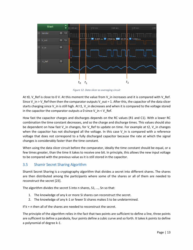
Figure 12. Data slicer as averaging circuit
At t0, V_Ref is close to 0 V. At this moment the value from V_in increases and it is compared with V_Ref. Since V_in > V_Ref then then the comparator outputs V_out = 1. After this, the capacitor of the data slicer starts charging since V_in is still high. At t1, V_in decreases and when it is compared to the voltage stored in the capacitor the comparator outputs a 0 since V_in < V_Ref.
How fast the capacitor charges and discharges depends on the RC values (R1 and C1). With a lower RC combination the time constant decreases, and so the charge and discharge times. This values should also be dependent on how fast V_in changes, for V_Ref to update on time. For example at t2, V_in changes when the capacitor has not discharged all the voltage. In this case V_in is compared with a reference voltage that does not correspond to a fully discharged capacitor because the rate at which the signal changes is considerably faster than the time constant.
When using the data slicer circuit before the comparator, ideally the time constant should be equal, or a few times greater, than the time it takes to receive one bit. In principle, this allows the new input voltage to be compared with the previous value as it is still stored in the capacitor.
3.5 Shamir Secret Sharing Algorithm
Shamit Secret Sharing is a cryptography algorithm that divides a secret into different shares. The shares are then distributed among the participants where some of the shares or all of them are needed to reconstruct the secret [23].
The algorithm divides the secret S into n shares, S1, so that:
1. The knowledge of any k or more Si shares can reconstruct the secret. 2. The knowledge of any k-‐1 or fewer Si shares makes S to be undetermined.
If k = n then all of the shares are needed to reconstruct the secret.
The principle of the algorithm relies in the fact that two points are sufficient to define a line, three points are sufficient to define a parabola, four points define a cubic curve and so forth. It takes k points to define a polynomial of degree k-‐1.
Page | 14
The algorithm creates the following polynomial to generate the shares,
(3.3)
Here, the Secret is assigned to the first coefficient of the polynomial and the rest of coefficients are generated randomly. The shares are then generated by constructing k different points with the form,
(3.4)
After receiving the shares, the polynomial can be reconstructed by computing the Lagrange Interpolation,
(3.5)
The Lagrange basis polynomials are found with,
(3.6)
3.6 Field Programmable Gate Arrays
Field Programmable Gate Arrays (FPGAs) are semiconductor devices that contain an array of programmable logic blocks connected via programmable interconnects. The logic blocks can be configured to perform combinational functions, or to perform as simple logic gates like AND, OR, and NOT gates. The logic blocks may contain flip-‐flops as memory elements or they can be complete blocks of memory.
The advantages of using FPGAs over other units is that they are sometimes significantly faster for some applications, since the computations can be performed in parallel on different logic blocks. Also they might become optimal in the sense that the number of gates are minimum for certain processes.
The circuitry inside an FPGA are synchronous blocks that require a clock signal. FPGAs have dedicated networks for clock and reset. Low power FPGAs operate with clocks between 20 MHz to 80 MHz, but there are more advanced FPGAs which operate at frequencies greater than 800 MHz.
For small applications, FPGAs provide exact interaction with logic blocks and clock signals in a way that no other processors can, making the logic time dependent.
The behavior of the FPGA is defined by the user with Hardware Description Language (HDL) files, by a schematic design, or a combination of both. The two most common HDL are Verilog and VHDL. Both describe the digital signals and their behavior inside the arrays. The selection on either of them relies on the ease of use for the programmer.
3.7 Linear Feedback Shift Registers
Random number are essential primitives when it comes to security applications. Secret keys, initialization vectors and the seeds for cryptographic algorithms rely on pseudo-‐random generators. These generator have algorithms for generating a sequence of numbers that are close to the properties of sequence of random numbers. However, the sequence is not truly random as it is determined by one or many initial values called seed [24].
Linear Feedback Shift Registers are sequential shift register with combinational logic that makes the registers to pseudo-‐randomly cycle though a sequence of binary values. The initial value for the LFSR is

Page | 15
called the seed, and since it is deterministic, the output of the registers is a function of its previous state. Choosing a correct feedback configuration makes the output to appear random [24]. Even though the states will cycle, the periodicity of the signal is driven by the number of n registers used as
(3.7)
The correct feedback will make the LFSR to achieve this maximum period. The feedback comes from selecting different registers (taps) in the chain of register and XORing these taps to feed the register back.
Figure 13. LFSR using shift registers8
3.8 Beam Spread
The beam spread is the plane where the intensity of the light is at least 50% of the maximum intensity at the center beam, and the field spread contains 10%, or less, of the maximum intensity [25]. For a surface perpendicular to the bulb the beam spread can be approximated by a cone, where the bottom creates a circular spot size calculated by,
(3.8)
8 http://www.ece.ualberta.ca/~elliott/ee552/studentAppNotes/1999f/Drivers_Ed/lfsr.html

Page | 16

Page | 17
Chapter 4 DESGIN CONSIDERATIONS
One of the goals in the project is to develop a comparator-‐based VLC security application for multiple lights. In order to construct such system, we make important considerations regarding the types of modulations and multiple light scheduling.
In this chapter we describe why two of the most common modulation schemes used in VLC should not be used in our system.
4.1 Modulations
We provide the following insights about why OOK and BFSK are not recommended for a multiple-‐light VLC system with a comparator-‐based receiver.
4.1.1 On-‐Off Keying
While OOK is the simplest modulation, it is also the most prone to errors when combined with a comparator-‐based receiver. In outdoor applications, light does not only depend on the transmitter but also on the environment. Here, the sun and the clouds have a significant impact on the amount of light incident on the photodiode. When the light intensity changes due to the environment the comparator interprets it as valid data and outputs erroneous results.
A workaround for these dynamic-‐light environment is to configure the photodiode and comparator to become less sensitive to light and voltage variations respectively. But this introduces another issue when the background light remains steady; the induced slow reaction affects the length of the signals in the output. To explain this further, l the 0101 bit string shown in the next figure.
Figure 14. Increased ON signal length with OOK
The low response of the comparator to the light fluctuations causes a delayed and almost doubled in size HIGH signal.
In an ideal transmission, the output signal must be as close as possible to the transmitted signal for the algorithm to interpret it correctly. Because of the size of the previous signal, the chances of interpreting it as 01101 are high.
4.1.2 BFSK
In BFSK one frequency is used to represent a 1, and a second frequency represents a 0. Usually when using this modulation scheme the same frequency is repeated over a period of time, and the decoding algorithm is responsible for checking which frequency is dominant.

Page | 18
Figure 15. Dominant frequency in BFSK9
One of the advantages of combining this modulation with a comparator and an FPGA is that a bit can be represented with a single signal instead of sending the same waveform multiple times. Figure 21 shows the representation for the bit pair 10 using BFSK.
Figure 16. Single signals for 10 string
There are three advantages of using this type of modulation over OOK:
1. It provides dependency between sender and receiver. The communication might still be affected by the change of light in the environment, but now the receiver is required to find a specific pattern in the medium.
2. The environment has the same effect over both bits. Either both representations increase their size (Figure 17), or both of them decrease their size (Figure 18). (These images s).
Figure 17. Duty cycle increased on both, 1 and 0, signals with BFSK produced by having background light
Figure 18. Duty cycle decreased on both, 1 and 0, signals with BFSK produced by removing background light
9 Figure Source: https://en.wikipedia.org/wiki/Frequency-‐shift_keying

Page | 19
While very promising, this modulation introduces a weakness into our security system. Since the user is required to obtain information from multiple lights, one light easily discloses information about the others. Figure 19 shows that by measuring the time between consecutive bits obtained from the same bulb we can deduce which bit is sent on the other bulb. Notice that the time marked by the blue arrow for LED2 is greater than the time marked by the orange arrow. This is because a 0 is being sent on LED1 during the blue line, and a 1 is being sent by LED1 during the orange line.
Figure 19. Security weakness from BFSK
In order to remove this security weakness the periods of the bits must be kept the same; by doing so, we are converting the BFSK signal into a PWM signal.

Page | 20

Page | 21
Chapter 5 DESIGN AND IMPLEMENTATION OF PHYSICAL LAYER
In this chapter we address the goals set for the Physical Layer. We describe the hardware configuration and explain how data is encoded into signals and how these signals are received and interpreted. We divide the system into two subsystems: Sender and Receiver.
The Sender consists of a network of LEDs, each one with its own driving circuit, and one FPGA encoding information to the bulb by controlling their drivers through GPIO pins. The Receiver consists of a circuit combination of the optical receiver OPT101 and the TS881 comparator connected to one GPIO pin of a second FPGA. The data decoded from the receiver is sent to the computer through UART communication from the mini-‐USB port, also meaningful information is displayed on the mounted LEDs of the board. The software runs on IGLOO Nano FPGA evaluation boards with AGLN250V2-‐VQG100 operating at a frequency of 20 MHz.
Figure 20. System diagram
5.1 Frame Structure
Since this is a secret-‐sharing application-‐oriented system we use a simple frame structure consisting of:
Preamble (two bytes) Header
o Number of shares (1 byte) o Size of payload (1 byte) o Epoch number (1 byte)
Payload o Start (1 byte) o Share (Fixed to 4 bytes) o End (1 byte)

Page | 22
Figure 21
The Preamble serves as the synchronizing instrument between Sender and Receiver; it is formed of 16 consecutive The Number of shares is left as an option for the user to choose how many shares are necessary to reconstruct the secret; this value is fixed to two shares. The Size of payload can be used as a redundancy check; accepting a new frame in the reception algorithm does not depend on the size of the payload, but rather on detecting a steady ON state of the lights after every frame. The Epoch number is used by the decryption algorithm in the Application Layer to receive new Shares. The Payload is fixed to 6 bytes; the first and last byte serve as identifiers of successful decryption of a Secret, and the rest four bytes correspond to a Share used to reconstruct the Secret.
5.2 Sender Subsystem
The Sender corresponds to the group of three LEDs, each with its own driving circuit, scheduled by a single FGPA. When lights are close enough and all being part of a system, a network of wireless sensor nodes can be substituted by an FPGA. For bigger applications however, a combination of both is the best approach.
5.2.1 Driving the LEDs
The LED bulbs used for the project are shown in Figure 22. They are driven by 12V, have a beam angle of 38°, consume 5W of power, and produce a luminous flux intensity of 320 lm. Each bulb has its own driver which turns the bulb ON and OFF when indicated by the FPGA. The driver is a constant current driver circuit. The LM350 voltage regulator allows the circuit to maintain a constant power on the LED, and the value of this current depends on the resistance attached to it (R1). An additional MOSFET allows to toggle the bulb ON and OFF. The driver circuit is shown in Figure 23.
Figure 22. Ledsaver 12 V, 38°, 320 lm

Page | 23
Figure 23. Circuit Schematic for LED driver
5.2.2 Pulse Width Modulation
We described in the previous chapter why different modulation schemes such as OOK and BFSK are not recommended for our system. OOK is prone to errors if not used in a controlled environment and it also introduces jitter in our design. BFSK is very promising but it represents a weakness for the security aspect.
Pulse Width Modulation provides a more robust and secure system. In PWM a pair of signals with different duty cycles are used to represent a 1 and a 0. We have chosen a duty cycle of 25% to represent a 0, and a duty cycle of 75% to represent a 1. This is because we compare the length of the signals to determine which one is bigger. If they are too closed together with more similar duty cycles then the comparison is not always correct. Figure 24 shows the PWM representation for the binary string 001100.
5.2.3 Scheduling the LEDs
The characteristic of the comparator makes it necessary to schedule multiple lights. The output that is given when multiple lights are ON is the same output that is given when a single light is ON. The comparator cannot differentiate the state of individual lights when they occupy the same ON period. Because of this reason, our multiple-‐light system requires the sender to transmit from only one light at a time while the rest remain OFF.
However, transmitting for a long period cause flicker to be noticeable. Hence, instead of sending the whole Payload at once we propose to schedule the lights in a bit-‐by-‐bit manner.
Figure 24. Binary string using PWM, 25% (0) and 75% (1) duty cycle
Page | 24
Figure 25. Bit-‐by-‐bit Scheduling of 3 lights
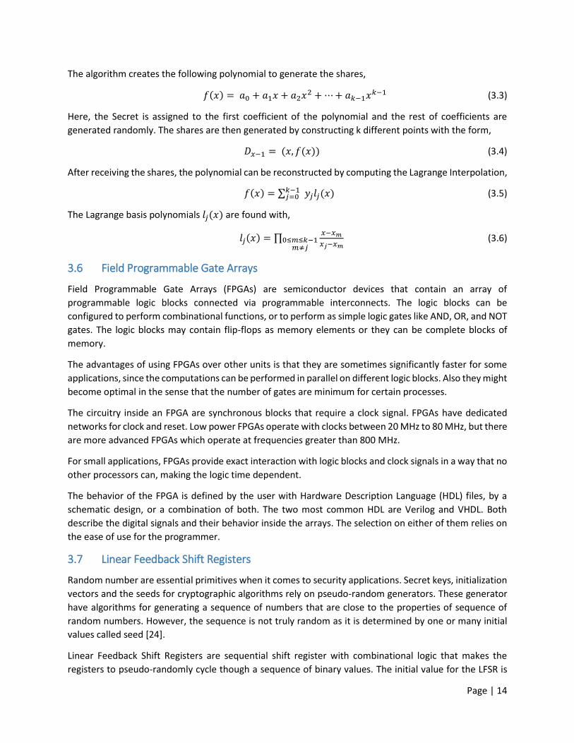
Figure 25 shows this proposal, each light is transmitting a piece of a Share:
1. When a new frame is ready to be transmitted, all the lights send the Preamble and Header simultaneously. When the Header is finished, the lights start to schedule in a predefined order.
2. Transmission is scheduled in ascending order L1-‐L2-‐L3-‐ -‐L1-‐L2-‐L3. 3. A light transmits one bit at a time, starting from its MSB and shifting towards its LSB. The bit is
transmitted over a period T while the rest of the lights remain OFF. 4. After the last bit from the last light is transmitted all the lights are turned ON. They remain in this
steady status for a predefined time Tk. Once Tk is over the Preamble and Header are sent again with a new Payload.
5.2.4 Encoding Algorithm
In order to generate the PWM signal in the FPGA, a simple counter-‐process was executed. The output is given by a dedicated GPIO pin for every light driver. The advantage of an FPGA in this case is that we can keep exact track of time by counting the 20 MHz (50 ns period) tick cycles.
To find the number of ticks corresponding to any transmission rate we divide the duration of one bit by 50 ns period.
When a new bit needs to be transmitted, the FPGA generates a HIGH signal for the light and starts a counter. At a rate of 10 Kbps, a binary 0 has 500 ticks HIHG and 1500 ticks LOW; a binary 1 has 1500 ticks HIGH and 500 ticks Low.
Appendix A provides technical details about the VHDL implementation of the scheduling and generation of bits.
5.3 Receiver Subsystem
The Receiver consists of the combination of the OPT101 photodiode and the TS881 comparator connected to the Igloo Nano FPGA through a GPIO pin. The photodiode has a feedback network circuit to improve its responsivity to light changes; the comparator has a data slicer circuit for proper comparison of signals. The photodiode detects the light intensity changes produced by the signal modulation of the Sender and transforms them into voltages. The TS881 accepts these voltages variations and compares them with a reference value. The comparator outputs only two signal values, a HIGH or a LOW. This serves as an analog to digital conversion. The output of the comparator is then accepted by the FPGA which measures the time from one LOW-‐to-‐HIGH transition to the next HIGH-‐to-‐LOW transition. This time is then compared with predefined periods corresponding to a binary 1 or 0. How the bits are stored and used for decryption is addressed in the next chapter.

Page | 25
5.3.1 OPT101 Feedback Network
The dynamic response of the OPT101 was improved with an external feedback network with CEXT and REXT as shown in Figure 26. Selecting different RC values for the feedback network modifies the response of the photodiode to different frequencies. Changing the responsivity also changes the gain, bandwidth, and rise time of the photodiode.
Figure 26. External Feedback for OPT101
One advantage of increasing the gain of the photodiode is that we make it more susceptible to light changes. This is helpful when we want the photodiode to be receptive in large areas away from the light source, or when well-‐defined light transitions are required for the comparator to execute correctly. The reception area of the receiver increases with a high gain configuration, because we are able to identify light variations when the receiver is away from the light source. A tradeoff however is that when increasing the gain, the bandwidth is reduced.
On the other hand, an advantage of decreasing the gain is that we can use the photodiode in environments with high light since we make it less susceptible to light. A tradeoff in this case is that even though we are able to transmit faster the reception area is reduced. This is because the photodiode can only identify strong light fluctuations which are found closer to the light source.
Modifying the gain of the photodiode is an important configuration for our application. Recall the Secret can only be reconstructed if the information is collected at the intersecting area of two lights. How the reception area looks like, is dependent on where the photodiode is able to detect light transitions containing data.
5.3.2 Data Slicer
The TS881 comparator is just an operational amplifier which outputs a 0 or a 1 depending on the voltage difference of the input voltage and reference voltage. How these values are set depend on an extra circuit before the inputs.
A simple voltage divider circuit can be used, but in order to build a more dynamic receiver the comparator requires the reference voltage to be dependent on the input voltage. To achieve this, we attach a Data Slicer circuit to the reference voltage which allows us to recover signals during transmission. Figure 27 shows the circuit connected to the op-‐amp of the comparator. V_in is the voltage value from the

Page | 26
photodiode. V_ref is the reference voltage after the data slicer circuit, and V_out shows the output of the comparator. We refer to the whole circuit as the comparator circuit.
Figure 27. Data Slicer configuration for comparator
The values of R1, R2 and C1 can be found for a specific time constant. The time constant affects how fast or slow the voltage in the capacitor changes, allowing a new input voltage to be compared with a previous value stored in the capacitor. Depending on the application and the environment in which the system is placed (i.e. with or without background light) the time constant can be really small, really large, or similar to the duration of one bit (i.e. based on the data rate). The effects of each are described in the Evaluation Chapter.
Because we are using a PWM scheme, when defining the time constant based on the data rate it should be defined according to the duration of the ON period of the 25% duty cycle signal. This is the fastest period in which the signal changes.
In order to evaluate the Receiver we performed experiment with data rates from 1 Kbps to 40 Kbps. Even though the receiver can be configured to data rates higher than 40 Kbps we stopped at this rate as it is already enough for our application-‐oriented system and we decided to focus our attention on other aspects of the design.
Table 1 shows the criteria under which a time constant is defined when compared to its data rate and the respective RC values. All of these settings work correctly at a distance of 1m to the source with no background light.
Table 1. Time constant based on signal duration
5.3.3 Reception Algorithm
The reception algorithm knows beforehand the length of each PWM signals. It is predefined that a signal with a duty cycle of 25% corresponds to a 0 and that a 75% duty cycle corresponds to a 1.
CriteriaData rate (Kbps)
Signal Duration (µs)
Time Constant (µs)
Ratio to the Signal (
R1 R2 C1
Large 100% of the signal's period
40 25 1120 0.02% 20 K 220 K 56 nF
of 25% of the period40 6.25 6.6 0.95% 20 K 220 K 330 pF
Small 100% of the signal's period
1 1000 6.6 151.52% 20 K 220 K 330 pF

Page | 27
To determine the duty cycle we measure the length of the ON period of the PWM signal and perform a 50% check. If the length is greater than 50% of the duration of one bit then the signal corresponds to a 1, on the contrary it corresponds to a 0. The length of the OFF period is not measured.
The algorithm does not keep track of the number of bits that have been received. Once it receives 16 as a pipeline to transmit incoming bits to the rest of
the blocks. This pipeline-‐like behavior ends when the algorithm stops detecting transitions within predefined periods of time.
If a light is missed during reception the algorithm produces a binary 0 as if it was the received bit. This is to maintain the structure of the light scheduling in order to correctly demultiplex the incoming bits for the reconstruction of the Secret.
Appendix B provides technical details about the VHDL implementation for receiving the bits and the watchdogs that allow new frame receptions.

Page | 28

Page | 29
Chapter 6 SECURITY APPLICATION
Communication with Visible Light is rapidly increasing and so are the applications developed around it. A concern in this type of communication, as in any other wireless communications, is the protection of information from potential attackers sharing the same medium.
In simple applications anyone with a photodiode would be able to detect the light changes from the bulb, and even able to retrieve information if the correct analysis is performed. However, the success in doing so can be extremely difficult if correct encryption algorithms are applied.
We propose in this chapter an application that can be used for security purposes. It encrypts the information before transmitting and it adds other levels of security for further protection. Our testbed consists of three continuous LEDSs that create two light intersections.
6.1 Application Overview
Figure 28. Testbed for the Security Application
We propose an application in which the user has to visit specific locations in a given sequence within specific time. We define these locations as the intersecting areas of two lights in order to constrain the areas in which the information is available for security purposes. To ensure the sequence and timing we take full advantage of the Shamir Secret Sharing (SSS) algorithm. We choose this algorithm since it is shown in [5] as a reliable method for encryption but also because the computations needed to reconstruct the information allows us to add the sequence and timing dependency. The algorithm divides a Secret into different shares assigned to each light. These shares are sent repeatedly by the lights during a time defined as epoch. When the epoch reaches its end a new polynomial is generated and transmitted. To ensure that the information is only available at the intersection of two lights we XOR each share with a random number for every transmission of the share in the epoch.
From the previous overview we divide the security of the application into five different levels:
1. The first level relies in representing the information as points of a polynomial. 2. The second level gives an order dependency by requiring the user to follow a certain path. 3. The third level introduces location dependency as it is required to be in the intersecting areas to
receive meaningful information. 4. The fourth level introduces time dependency in which the user is expected to move from one of
these areas to the next one before a deadline. 5. The fifth level is a basic XOR ( ) encryption of the information before transmitting.

Page | 30
To achieve such levels, we take advantage of the Shamir Secret Sharing (SSS) algorithm and combine it with pseudo-‐random bit strings for extra encryption and time dependency. In the SSS algorithm, we set k to be equal to the number of light intersections present in the system. With 3 aligned bulbs we can create 2 light intersections, i.e. k = 2. The IDs for each of the three bulbs are L1, L2, and L3.
6.2 Encryption of the Secret
Secret refers to any type of information that we want to transmit. For our application we want to transmit a security Key consisting of 6 bytes. Figure xx shows the payload in the frame for the example Key
are necessary for the user to identify a successful reception of the Key when it is transmitted to a terminal. The remaining four bytes correspond to any alphanumeric characters. For the rest of the chapter we will refer to these 6 bytes as the Secret.
Figure 29. Example of a Secret
6.2.1 Security Level # 1: Polynomial
Based on the SSS algorithm we provide the first level of security by building a polynomial of the form to represent the Secret. We select k = 2 since our system has
2 light intersections which results in a polynomial of the form . As part of the algorithm, the unsigned representation of the Secret is assigned to the coefficient. However, even though our Secret is fixed to 6 bytes it is impractical to perform operations based on the bit-‐length of the Secret. For a Payload of more than 50 bytes, operations of 400 bits need to be done. Therefore, we opt to generate one polynomial for every character in order to create different points that are concatenated to form a Share before sending. We assign the unsigned representation of each byte in the Secret to the coefficient for each polynomial.
In order to create the points from the polynomial we generate an 8-‐bit random coefficient . This coefficient is kept the same for all polynomials for the duration of one epoch. This allows the receiver to check for stability when each byte is received since each share is only stored if it has been continuously received for a specific number of times. Keeping fixed for the duration of one epoch introduces an
when computing the points, however this can be balanced with the fact that this value is not visible outside an intersecting area because they are XORed with a different random number every time they are sent.
Table 2 shows the polynomial assuming . To construct the Shares, we find 2 points for each polynomial in the form . Table 3 shows the points generated for our Secret.

Page | 31
Table 2. Polynomial for each byte in the Secret
Table 3. Points for each byte in the Secret
6.2.2 Security Level # 2: Path Dependency
Each of the f(x) terms of the points calculated above can be represented as 8-‐bit unsigned numbers, these correspond to and . A Share is formed by concatenating each of the f(x) terms which result in and . In our case correspond to the concatenation of the f(x) terms of and correspond to the
concatenation of the f(x) terms of .
Since we are only sending the f(x) term in the Shares we can introduce the path dependency. In order to reconstruct a Secret both, x and f(x), terms are needed; but if x is predefined in the equation of the decryption algorithm then the computation gives a correct result only if f(x) is received in the correct order.
6.2.3 Security Level # 3: Intersecting Areas
The third level of security is introduced by splitting and before sending. This relies in the fact that if we take a random number and assign it to L2, and set another number and assign it to L1, then by obtaining the information from both lights and XORing them together we end up with since
. Since our system has only three lights, we can define and. Figure 30 shows this concept with the two intersections. If and are received in the correct
intersecting areas then the points and can be obtained to reconstruct the secret.
Figure 30. Share distributed in two lights
6.2.4 Security Level # 4: Time Dependency
The fourth layer of security requires the user to move from one intersection to the next one within a certain time period, we call this period an epoch. This is achieved by changing the polynomial and
Byte Polynomial f(x)K 75 + 51xA 65 + 51x1 49 + 51xb 98 + 51x2 50 + 51x. 46 + 51x
Byte D0 D1
K (1,126) (2,177)A (1,116) (2,167)1 (1,100) (2,151)b (1,149) (2,200)2 (1,101) (2,152). (1,97) (2,148)

Page | 32
calculating new and for every epoch by generating a new coefficient . The behavior is shown in Figure 31. Each row corresponds to a specific epoch , and each column represents the number of the intersection.
Figure 31. Shares available during an epoch.
The order dependency that we introduced before requires us to send at any epoch , and at the next epoch . This allows the user to move from one intersection to another and enables him to receive both Shares within two consecutive epochs. Obtaining the Shares in the correct order within two consecutive epochs results in a successful reconstruction of the Secret. A few highlights on this approach:
1. A new is being sent at every epoch. Its corresponding is sent in the next epoch. 2. It is impossible to go back in time, i.e. obtaining under intersection 2 at any and moving to
intersection 1 to obtain its corresponding is not possible because of #1. 3. If after obtaining from intersection 1, the user takes longer than an epoch to reach intersection
2, the obtained does not correspond to the same polynomial.
6.2.5 Security Level # 5: XOR Every Frame
The fifth security level is obtained by XORing a random generated number with , and before sending. In this case , and are assigned to L1, L2, and L3 respectively. Even if an attacker is able to obtain the information from a light, it does not disclose information about or . This procedure is done for every new frame that is sent. The random number is generated by the FPGA using the Linear Feedback Shift Register mentioned in Chapter 2.

Page | 33
6.2.6 Combined Security Levels
Figure 32. Combined Security Levels
Figure 32 is a more detailed diagram all the levels of encryption:
1. A new polynomial is generated for every epoch to obtain new and shares. This is achieved by generating a new coefficient for every epoch. The must remain the same since it is the unsigned representation of each byte in the Secret.
2. The Shares are split into parts by generating a random value of and setting and . The random value of b does not change for the duration of an epoch.
3. and are assigned to L1, L2, and L3 respectively. 4. An epoch contains N number of rounds in which and are transmitted repeatedly. Because
transmission happens at rates of Kbps the information must be available for at least N rounds to allow the user to obtain it.
5. and are XORed with a new random number for every round that they are sent. This number is different for every round in every epoch.
6. can be obtained at every epoch and its corresponding delayed for it to be obtainable on the next epoch.
7. Reception of the shares in two consecutive epochs lead to a successful reconstruction of the secret.
8. Numerals 2 and 3 from Section 6.2.4 are still valid for this diagram.

Page | 34
In the algorithm, the number of N rounds control the time between each epoch. For a Secret of 6 bytes our modulation scheme requires 0.01392 seconds to transmit one round. If we want to transmit in an epoch of 5 seconds we must set N = 360. If we want to transmit during an epoch of 2 seconds we set N = 143.
6.3 Decryption of the Secret
Each of the incoming bits interpreted by the Reception Algorithm from Chapter 5 are assigned to one of the three compilation blocks depending on its position in the receiving signal pattern. It is predefined in the algorithm that the incoming bit stream correspond to the bit-‐schedule L1-‐L2-‐L3-‐L1-‐L2-‐L3-‐ -‐L1-‐L2-‐L3. Knowing this schedule allows to demultiplex the bit stream into the corresponding bytes for each light. L1 bits go to a byte compiler named , L2 bits go t , and L3 bits go to . This allows us to have the same
structure in which the data was encrypted.
The decryption of the Secret is performed inside the FPGA. When a successful Secret is decrypted, it is sent to a terminal in a computer such as RealTerm through UART communication.
6.3.1 XOR Encryption and Shares
After a complete byte for is received we perform the operation, and after a complete byte for is received we perform the operation. By doing so, not only we remove the XOR encryption with a random number for every new frame, but we also obtain the unsigned representation of the points and for each byte in a Share. We wait for the and points of each byte in the Share.
6.3.2 Time Dependency
Before storing the Shares into dedicated registers, we check if they remain unchanged for a period of time. This allows us to remove the erroneous information produced when moving from one intersection to another. There are two ways for error removal, the tradeoffs for each are described in the Evaluation Section:
1. Store a new share if it remains unchanged for a specific time. This always keeps updating new shares and is independent on the epoch.
2. For a new epoch, always store the first Share detected if it remains unchanged for a specific time. A new share can only be stored again only when a new epoch arrives.
After checking that the Shares remain unchanged, we delay for further computations. This is done because every arrives one epoch later than . We need to ensure that for every new we perform the correct computations with its corresponding .
6.3.3 Path Dependency and Reconstruction of Polynomial
To satisfy the path dependency we fix the terms of the Lagrange basis polynomials from Equation 3.6 to and , and we also fix the relation from Equation 3.5. This can be done since
corresponds to the terms of the points and corresponds to the terms of the points .
For our 3 light system,

Page | 35
The Lagrange basis polynomials are:
(6.1) (6.2)
And the polynomial for each byte in the Secret obtained from the fixed relation in Equation 3.5 is
(6.3)
If the Shares are received in the correct order and within two consecutive epochs then the computation of the above equation results in the correct reconstruction of the Secret, in which the free term in the polynomial corresponds to the unsigned 8-‐bit representation of each byte in the Secret.

Page | 36

Page | 37
Chapter 7 EVALUATION
In this chapter we present a thorough evaluation of our system. We evaluate the following:
The performance of the receiver by modifying the circuit configurations of the comparator and the photodiode.
The BER for a large time constant in the comparator circuit, and the reception with different light intensities by varying the distance to the sender. This is performed for different data rates for scenarios with background light and without background light.
The sources of errors; based on these we perform experiments to define the impact of the data slicer circuit.
The responsivity of the photodiode to different gain configurations, where we define the reception areas for different gains. We use these areas to model a system with multiple lights.
Effects of having different duty cycles for the PWM signals The security application in which we identify the rates at which the user is able to walk to receive
the Secret.
We present screenshots from readings of a logical analyzer to explain the performance of the circuits.
7.1 Receiver Circuit
The purpose of performing the following experiments is to evaluate the Physical Layer in order to find the best configurations for the receiver that work under different light conditions. We start the evaluation of the receiver with a working prototype We choose this configuration because it works for data rates of 1 Kbps and 15 Kbps and we continue to examine its limits.
The following images show the readings from a circuit where the settings of the feedback network of the 6 V/A and a bandwidth of 44 KHz. The
settings of the data slicer circuit are . These settings prove to work at rates of 1 Kbps and 15 Kbps with the receiver placed at a distance of 100 cm from the sender. The signal Sender is the signal sent by the Sender. V_out corresponds to the output from the comparator. V_in is the input voltage to the comparator, and V_Ref is the reference voltage of the comparator.

Page | 38
Figure 33. Output signal at 1 Kbps for large time constant
Figure 34. Output signal at 15 Kbps for large time constant
We can observe from Figure 31 that the reference voltage remains steady. is too large compared to the duration of one bit. This makes the input voltage to be compared with more averaged value. Notice from the measurement in the V_in signal that Vpp = 0.5235 V, and that V_Ref = 0.289 is close to 0.5235/2.
This large time constant of the comparator is kept for the following experiments since it shows to work with data rates of 1 Kbps and 15 Kbps.
7.2 Bit Error Rate
Here we explore the limits of the previous configuration by finding the BER for different light intensities and transmission rates. Varying the distance from the photodiode to the sender results in different luminous power levels. We present two scenarios, with background light and without background light.
We require the Preamble and Header bytes to be detected to include the result in the BER metric. Failure to do so is considered in BER of 100 %. A random binary string is sent as Payload.
7.2.1 No background light
We use only one bulb for this experiment. The bulb is directly facing the photodiode. The distances from the photodiode to the bulb vary from 25 cm to 270 cm. Table 4 shows the illuminance, in lx, corresponding to these distances at rates of 15 Kbps and 50 Kbps; we remove the rest because the values remain close.

Page | 39
Table 4. Illuminance in lx at different distances, no background light.
Figure 35 shows the BER for these experiments. A few highlights when understanding the image:
At 10 Kbps, 15 Kbps, and 20 Kbps the data is received for all the distances except when the receiver is too close to the light source where it saturates.
Transmission at 25 cm is not possible for any data rate because of the saturation of the photodiode.
Transmission at high data rate with BER of 0% can only be achieved at 100 cm with 40 Kbps. A rate of 50 Kbps does not longer work for any distance.
Figure 35. BER without background light
7.2.2 Background light
For this scenario we introduce background light provided by a fluorescent lamp close to the sender. The illuminance of this lamp at a distance of 270 cm is approximately 400 lx. The following table shows the illuminance, in lx, at different distances for rates of 15 Kbps and 50 Kbps.
Table 5. Illuminance in lx at different distances, background light
Rate (Kb/s) 270 cm 250 cm 200 cm 150 cm 100 cm 50 cm 25 cm15 69 76 125 218 484 1700 985050 71 80 125 231 545 1988 1143
Rate (Kb/s) 270 cm 250 cm 200 cm 150 cm 100 cm 50 cm 25 cm15 254 294 440 625 760 1880 1020050 418 485 727 970 920 2060 10590

Page | 40
Figure 36. BER with background light
Figure 36 shows the results. A few highlights to understand these results:
High data rate of 35 Kbps can only be achieved at a distance of 100 cm with a BER of 0% At 10 Kbps and 15 Kbps data can be transmitted for all the distances except 25 cm where the
photodiode saturates. Transmission starts to fail for rates above 30 Kbps.
7.3 Causes of Errors
In order to understand why the bits from the previous experiments are received incorrectly during transmission we examine the performance of the comparator circuit. We present waveforms registered by a logical analyzer for each node shown in the comparator circuit.
Figure 37. Circuit of the comparator
7.3.1 No background light
The following waveforms correspond to a distance of 270 cm at 25 Kbps with no background light present. The signals show a considerable delay between each other. The length of the ON period is reduced in the
. V_out shows the output of the photodiode.

Page | 41
Figure 38. Reduced ON period , no background light.
We observe that the small voltage variations and the large of the comparator make the circuit to respond slower. The voltage must be big enough to trigger an ON transition in the comparator. When this happens, most of the ON period of the incoming signal has passed already. This results in the reduction of the duty cycle, which in turn gives an incorrect result for the 50% check required by the reception algorithm.
The following two waveforms are for a distance of 25 cm at 15 Kbps and 20 Kbps. The output of the photodiode (V_out) shows only a few transitions for 15 Kbps and none for 20 Kbps. This is because the photodiode is close to its saturation region and the light levels are too high to identify its transitions.
Figure 39. 15 Kbps at 25cm close to saturation region
Figure 40. 20 Kbps at 25cm close to saturation region
7.3.2 Background Light
When we introduce background light by adding a fluorescent lamp next to the sender, a new error in the form of noise emerges. This is caused by fluctuations of the fluorescent lamp, but it is only present at long distances.
The following waveform corresponds to a distance of 250 cm at 15 Kbps. In this case, the noisy signals
check.
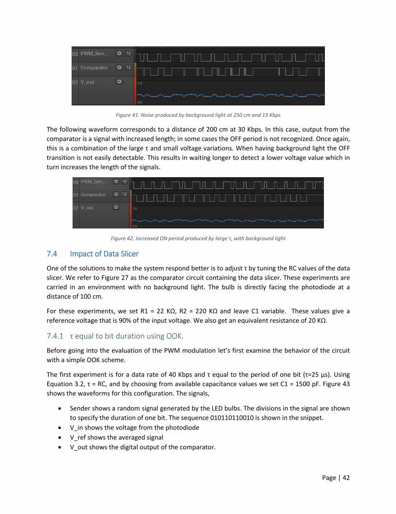
Page | 42
Figure 41. Noise produced by background light at 250 cm and 15 Kbps
The following waveform corresponds to a distance of 200 cm at 30 Kbps. In this case, output from the comparator is a signal with increased length; in some cases the OFF period is not recognized. Once again, this is a combination of the large and small voltage variations. When having background light the OFF transition is not easily detectable. This results in waiting longer to detect a lower voltage value which in turn increases the length of the signals.
Figure 42. Increased ON period
7.4 Impact of Data Slicer
One of the solutions to make the system respond better is to adjust the RC values of the data slicer. We refer to Figure 27 as the comparator circuit containing the data slicer. These experiments are carried in an environment with no background light. The bulb is directly facing the photodiode at a distance of 100 cm.
For these experiments, we leave C1 variable. These values give a reference voltage that is 90% of the input voltage.
7.4.1 duration using OOK.
Before going into the evaluation of the PWM modulation first examine the behavior of the circuit with a simple OOK scheme.
The first experiment is for a data rate of 40 Kbps and Using Equation 3.2, , and by choosing from available capacitance values we set C1 = 1500 pF. Figure 43 shows the waveforms for this configuration. The signals,
Sender shows a random signal generated by the LED bulbs. The divisions in the signal are shown to specify the duration of one bit. The sequence 010110110010 is shown in the snippet.
V_in shows the voltage from the photodiode V_ref shows the averaged signal V_out shows the digital output of the comparator.

Page | 43
Figure 43
We observe that with this configuration the comparator provides a correct result. However, there exists a small delay in the output signal.
7.4.2 smaller than bit duration using OOK.
For the next experiment we keep the same RC values but now we change to a slower data rate of 1 Kbps. The sequence 010110010101 is shown in the snippet.
Figure 44
In this case, the output of the comparator does not correspond to that of the sender. The falling edge is in fact followed correctly, but notice how after every falling edge of the Sender the comparator gives a false positive. To explain this, we augment the segment in which the false positive occurs in Figure 45.

Page | 44
Figure 45. False positives from data slicer
The small time constant of the comparator (25 µs) makes the voltage in the capacitor to charge and discharge at a very high rate. This is the reason why the V_Ref signal looks exactly like V_in. The comparator responds to the small voltage variations in the above figure by triggering the false positives.
The resistor R2 in the circuit has also a big influence on this behavior. It brings the input voltage to a lower voltage, 0.90 of the input voltage in our case. If the input voltage remains steady then R2 keeps the reference voltage lower than the input voltage, and the expected output is HIGH from the comparator. The output can still remain LOW if the difference between the voltages are below the internal threshold of the comparator. If the difference increases, then comparator outputs a HIGH signal.
7.4.3 to 25% duty cycle using PWM
Our PWM has the following two bit durations:
1. The duration of the ON period of the 25% duty cycle 2. The duration of the ON period of the 75% duty cycle
We adjust the comparator circuit For the next experiment we send at 40 Kbps and We showed above that having small for slow data rate makes the comparator more susceptible to voltage variations. We were expecting the same
however, the following experiment shows the opposite.

Page | 45
Figure 46 correspond to a data rate of 40 Kbps using capacitor value of C1 = 330 pF. We observe a correct behavior from the comparator.
Figure 46 25% duty cycle
7.4.4
When understanding why the comparator does not trigger the false positive in the previous experiment we assume that 6.25 µs is only 1/4 of the total period and that the small v
Therefore, we make the ratio even longer by increasing the length of the signal by reducing the data rate. The next waveform corresponds to a data rate of 1 Kbps with the same time constant of 6.25 µs.

Page | 46
Figure 47
We observe that the output is still correct. Even though this configuration still behaves correctly, the risk for getting false positives still exists if any sudden voltage variations is present. A system with background light as depicted in the BER section would make the comparator trigger false positives because it is more responsive to the variations of the background light.
At this point we stop modifying the circuit as we have presented useful information for different types of light conditions and data rates. We identified cases in which large time constants is preferable over small time constants, and the opposite. For our Security application, sending above 10 Kbps suffice our purpose.
7.5 Photodiode
We have presented until now how the receiver works by modifying the comparator circuit. However, the data reception is also influenced by the settings of the feedback network of the photodiode and by the voltage driving it.
7.5.1 Saturation
We perform the following experiment to understand the saturation value and to show its dependence to the driving voltage.
For this experiment an OOK modulation The illuminance from the bulb at this point is 8 lx. Figure 48 shows the results with the photodiode driven by 3.3 and Figure 49 shows the photodiode driven by 6V.

Page | 47
Figure 48. Photodiode driven by 3.3 V
Figure 49. Photodiode driven by 6 V
When driven by 3.3 V, the photodiode reaches its dynamic range for which it saturates. When driven by 6 V the photodiode is still under this range and the transitions are still recognized.
7.5.2 Responsivity Single Source without Background Light
The following experiment show the performance of the photodiode when we adjust its responsivity.
The purpose of these experiments is to show how different gain configurations affect the reception area of the information. Remember that in a system with more than one LED each bulb has its own slot to transmit one bit, and during this slot the rest of the lights remain off. Since the data transmission occurs at a speed of , all the LEDs seem to be ON all the time. Because of this, we can model the reception area for multiple light sources by collecting the results only from one LED.
The following table shows the RC values used for these experiments, along with the rated responsivity and bandwidth for each configuration.
Table 6. Responsivity and Bandwith configurations
We present the results in form of heat maps. Each map shows the beam and field spread of the LED in blue. The beam spread is represented with a darker blue circle in each graph; but it is not noticeable for the high gain configuration as it is covered by the reception area. The field spread is shown as a blue gradient; notice that these are not readings of actual light but only a shadow describing the behavior. The reception area of the key is shown in green. The beam angle of the LED is 38°. The bulb was placed at a height of 265 cm from the ground. The inclination angles of the bulb are measured with an imaginary line perpendicular to the floor as shown in Figure 50.
ConfigurationREXT
(MCEXT
(pF)DC Gain
Bandwidth (KHz)
LOW GAIN 0.05 56 0.05 58HIGH GAIN 2 NA 2 9.4

Page | 48
Figure 50. LED placed
The beam spread of the light with the LED at 0° angle can be modeled by a cone facing the ground. At a distance of 265 cm with an aperture angle of 38° and using (3.8) we calculate the spot size to be 182 cm.
To calculate its length we use basic trigonometry with the cone model as basis. The width is also calculated with (3.8). We show this elliptical shape with a darker blue in the following heat maps.
The results are shown in two columns, high vs. low gain configurations; with 45, 35, 25, 15 and 0 degrees of inclination and no background light. The source is placed at (0,200).
Figure 51. High (a) vs. Low (b) gain at 45°
Figure 52. High (a) vs. Low (b) gain at 35°

Page | 49
Figure 53. High (a) vs. Low (b) gain at 25°
Figure 54. High (a) vs. Low (b) gain at 15°
Figure 55. High (a) vs. Low (b) gain at 0°
The results show that the higher the gain, the more difficult it is to detect fluctuations in light. The photodiode does recognize the small fluctuations of light when we go away from the source. For the High gain configuration, the reception area is not constrained to the theoretical spot size; it also covers the majority of the field spread. This is because with a high gain, small fluctuations are more detectable.
In theory, the spot size increases as the angle increases and a larger reception area is expected. But the Low configuration shows an increased reception area while decreasing the angle. This is because the low fluctuations of light are not detectable for the low gain of the photodiode, and so the reception area is closest to the center of the spot size.
7.5.3 Responsivity Single Light with background Light
Figure 56 shows the reception area of the low gain configuration when background light of 400 lx is introduced to the system. The purple shadow is just a representation of a uniform background light.

Page | 50
Figure 56. Reception area at 0° with background light Low gain
The results show that with a low gain the impact of the background light is reduced, but it is also more difficult to detect the fluctuations from the source. The information is received only at a close distance to the source. For the high gain configuration, the photodiode is saturated and the key cannot be received at any point.
7.5.4 Responsivity Multiple Lights
For a multiple light system, the reception area can be modeled by creating a mirror of the results of a single source. From one source we can model how close the lights need to be placed to create a decent intersection. Figure 57 shows the mirror of the results for a high gain configuration at 0° (from Figure 55(a)). Figure 58 shows the mirror of the results for low gain at 25° (from Figure 53(b)).
The blue and purple shadows represent the two sources. The green shadow is the reception area of a single source. The red shadow shows the reception area in the intersection of the two lights. The closer the sources are placed, the bigger the reception area.
Figure 57. Mirror of High gain at 0°
Figure 58. Mirror of Low gain at 25°
7.6 Flickering
When we model the reception area with two lights, flickering is unnoticeable. But once we introduce a third light to evaluate the security application, flickering becomes noticeable. The problem increases as more lights are introduced into the system. Two reasons for this are:
1. -‐OFF light proportion. 2. The scheduler increases the OFF proportion of each light because it needs to remain OFF while
the other transmit their bits.

Page | 51
Some workarounds to reduce flickering are:
To increase the data rate. Flickering was more noticeable when we using 10 Kbps than when using 30 Kbps.
To modify the duty cycles. We modify the duty cycles from 25% and 75% to 30% and 70% and it reduced the flickering. We also performed experiments with 40% and 60% but even though it removes the flickering completely, the signals are too similar for the receiver to perform the 50%-‐check to demodulate.
Adjust the receiver to work with background light so that the flicker of the sources have no impact at all.
7.7 Security Application
The evaluation of the application is a combination of fulfilling the requirements from the Objectives section and evaluating it under different walking speeds.
A tradeoff of adding time dependency is that the application has to be pre-‐configured for each required walking speed. This is because the Secret can only be decrypted within consecutive epochs; which defines the walking speed. Slow walking speed requires the epoch to change slower; fast walking speed requires the epoch to change faster:
If it is configured for fast walking speed but the user walks slower, he reaches the next intersection after the required epoch.
If we configure it for a slow speed but the user walks faster, he will reach the next intersection within the same epoch which is sending a different Share. If method # 2 for error removal (section 6.3.2) is used, then the user needs to wait for a new epoch before moving to the next intersection. If method # 1 is used, then the algorithm accepts the new Share and the Secret cannot be decrypted.
An average walking speed is about 1 m/s. If the lights are 1 m apart, an appropriate duration for an epoch is twice the duration to walk this distance, i.e. 2 s. This gives enough time to the user to reach to the next epoch.

Page | 52

Page | 53
Chapter 8 CONCLUSION AND FUTURE WORK
In this chapter we discuss the results drawn from previous sections. We also mention some of the limitations of the design and discuss areas of improvement.
8.1 Physical Layer
From the experiments we performed in the previous chapter we can conclude the following:
For the comparator:
The recommended configuration is with a time constant equal to the duration of one bit. For our PWM modulation the best performance is given with a time constant equal to the duration of the on period of the 25% duty cycle signal.
Using a time constant smaller than the duration of one bit improves the response of the comparator but also makes it more vulnerable to light fluctuations. This is recommendable for low light conditions.
Using a time constant larger than the duration of one bit reduces the effects of the background light, which makes it better for high light conditions. If it is too large, the data slicer outputs a steady value similar to the average of the peak-‐to-‐peak values of its input voltage.
The points above only give recommendations of what is the best configuration depending on the environment in which the application is used. There is not any configuration that works under all conditions, but rather it is specific for each environment. Once the environment is defined, it can be configured to achieve higher data rates. Even though high data rates are not needed for the application, they are necessary to remove the flicker from the lights.
For the photodiode:
Low gain configurations allow us to achieve higher data rates but limit the reception as we move away from the source. This configuration is recommendable when background light is present.
High gain configurations increase the reception area but it limits the data rate. Also, the photodiode saturates when background light is present under this configuration.
The saturation area of the photodiode is dependent on the voltage driving it. We were able to receive signals when driving at 6 V for an illuminance of 8 lx, but it was saturated when driven by 3.3 V.
The results from inclining the bulbs when measuring the reception area serve to model the distances at which two different lights can be placed away from each other to form an intersection. The reception area increases with higher angles.
The bandwidth of a photodiode is also a limitation to achieve higher data rates. The photodiode can be modified to allow higher data rate but it is also dependent on how it should respond to the amount of light present in the medium. Higher bandwidth is achieved with a lower gain configuration; however, it reduces the reception areas. An interesting case of study for future work is to explore how more sensitive

Page | 54
photodiodes help to improve the performance of the system to achieve higher data rates and wider reception areas.
For the Scheduler:
The proposed scheduling algorithm shows flickering when using three lights and above. Keeping all lights OFF while one is transmitting changes the proportion of ON-‐FF times. However, using a comparator as a receiver enforces the use of this type of scheduling.
Flickering is reduced as the data rate increases and as the duty cycles are closer to be equal. 10 Kbps produces more flicker than 30 Kpbs. Also, 25% and 75% duty cycles produce more flicker than 30% and 70% duty cycles.
There is room for improvement in removing the flicker. Some improvements can be:
Finding a better scheduling algorithm. For example, adding dummy signals that turn on every light after sending each bit can help to make the cycles more proportioned. If the dummy signal is considerable longer than the period of one bit then the flicker would be removed; but the data rate would be considerably reduced.
Configuring the responsivity of the comparator and photodiode to allow for higher data rates and to use similar duty cycles.
Using a better photodiode with higher bandwidth to allow for higher data rate.
8.2 Application Layer
The application performs well with no background light conditions. When having background light the reception area is reduced which requires the lights to be significantly closer to form a well-‐defined intersection.
In addition, if the lights are too close together the receiver might be able to detect the information from all the lights, which makes the Secret always available. An improvement in this matter is to set up the system with an even number of lights and to use each pair for one different intersection away from the rest. This also removes the flicker completely as only two lights need to be scheduled.
An interesting step for future work is to study how the effect of improving the receiver affects the security of the information. With this application we want to make the information available at specific areas, but as the receiver improves then this constraint is reduced since the area where the information is available increases.

Page | 55
APPENDIX A VHDL Encoding Algorithm
The algorithm assumes that the part of a Share is already distributed to each light, and it is iterated bit by bit. The iteration is carried out by the rising edge of the same output signals to the bulb.
Figure 59. Top Level Schematic of the Encoding Algorithm
Top-‐Level Schematic
Figure 59 shows a top-‐level schematic for the PWM encoding algorithm. As input signals we accept the following:
reset is a general reset signal controlled by push button. clk is the 20 MHz clock. send_msg tells the block when to send a new frame. preamble_end tells if all the bits of the header have been sent. LED1_end informs when all of the LEDs have finished transmission. We only care about this one
because we always loop back to it for new transmissions. bit_in, bit_in_L1, bit_in_L2, and bit_in_L3 tell the next bit to be transmitted.
As output signals we have the following:
sift_en_pre, shift_en_l1, shift_en_l2, and shift_en_l3 enable the iteration on each light. clk_out1, clk_out2, and clk_out3 are assigned to the GPIO pins of the FPGA to control the lights.
They output a HIGH or LOW signals to represent the bit. end_key tells the other blocks that a complete frame has been transmitted.
The general reset button of the board must be pressed after powering it up. This ensures the internal registers, counters, and state of the FSM to be initialized correctly.
Algorithm using FSM
The algorithm is carried out by a FSM with the following states:

Page | 56
While in the Idle state we wait for send_msg in order to start the transmission. When received, we move to the Pilot state. Pilot It counts up to ticks_high with a HIGH output and up to ticks_low with a LOW output. After 16 bits we move to the Preamble state. All the lights are ON at this point.
In the Peramble state, if the incoming bit of the preamble message is a 1 we wait until the counter reaches ticks_high, if it is a 0 we wait until it reaches ticks_low. Once reached, we toggle the output signal and move to wait_preamble. Here we count up to the remaining part of the signal, ticks_low if the incoming bit is a 1 or ticks_high if it is a 0. We cycle between these two states until we receive the signal from preamble_end that all the bits of the preamble have been sent. We enable shift_en_l1 in order to shift the first bit of the first light and then we move to LED1. All lights are OFF at this point.
In the LED1 state we turn LED1 ON and keep the other lights OFF, we also store the current state into a register in order to define future transitions. We move to delay in which we store the value of the incoming bit into a register. Next we move to high_part. Here we check the value of the bit stored in the register to represent its ON section. If the value is a 1 we count until we reach ticks_high, and if the value is a 0 we count until we reach ticks_low. Once reached, we turn the light OFF and move to low_part. In this state we represent the OFF section of the signal. If the value in the register is a 1 we count until we reach ticks_low, or until ticks_high if the value is a 0. Once reached, we check the state register in order to define where to go next. Since we are just starting, we move to LED2.
In LED2 all the lights are OFF except LED2 and shift_en_l2 is enabled. This state sends us back to the delay state. The same instructions as above will be executed until reaching low_part, but since we come from LED2 we move to LED3.
In LED3 all the lights are turned OFF except LED3 and shift_en_l3 is enabled. We go back to delay and cycle until reaching low_part. As LED3 is the last light in the system, we go back to LED1.
This process keeps repeating until we receive the signal from the LED1_end input that the message from this light has finished. We go back to the Idle state in which we wait again for send_msg signal, all the other blocks except the preamble are disabled. All the lights are turned ON.
Page | 57
Figure 60. FSM of Encoding Algorithm

Page | 58

Page | 59
APPENDIX B VHDL Reception Algorithm
This describes in details the VHDL implementation of the Reception Algorithm
Top-‐Level Schematic
Figure 61. Top-‐Level Schematic of Receiver Algorithm
Figure 61 shows a top-‐level schematic of the PWM detection algorithm. As input signals we accept the 20 MHz clock, a general reset signal controlled by a push button, and the output of the comparator (comp_in). The essential output signals are:
Bit_ready lets other blocks to know that a new bit has been received Bit_in outputs which bit has been received Reset_idle is a reset that clears memory registers on other blocks of the design when the
algorithm is in the Idle state. The Idle state is reached when no change in light occurs (e.g. after a packet finishes transmission).
The other signals are used for debugging purposes and their use can be extended in future applications.
The general reset button of the board must be pressed after powering it up. This ensures the internal registers and state of the FSM to be initialized correctly.
Algorithm using FSM
While in the Idle state, we are sampling for a continuous HIGH signal. We do this by filling up four registers with the incoming signal of the comparator at every rising edge of the 20 MHz clock. We take this approach since the usual approach misses the edge. Normally, when checking for a rising edge of a signal inside a rising-‐edge triggered process, a register signal saves the incoming signal. When the signal is 1 and the register is 0, it means that there is a rising edge.
However when it was tried in our design, we identified that the signal was missed when the rising edge of the clock was in sync with the rising edge of the comparator. As we are unaware of the internal

Page | 60
architecture of the FPGA we assume that at this point a type different than a logic 0 or 1 was assigned to the register of the comparator. In the next clock cycle a 1 is assigned to this other type and it would not execute any instruction. At this point, the register is assigned with a new value of 1 which in turn results
-‐some of the valid signal types in VHDL).
Once the oversampling returns a detection of a steady HIGH signal, we go onto waiting for a steady LOW signal. We do this instead of enabling the counter to check for the length of the HIGH signal when a falling edge arrives, which will give us incorrect information as the user can enter the system at any given moment.
Once we have a steady LOW signal we go into another state (detect_high) that waits for the next HIGH
the Receiver. The detect_high is used by the algorithm as means to calculate the time it takes (in ticks) from one falling edge to the next rising edge. This is done for the following reasons:
When number of ticks from the falling edge to the rising edge is,
1. less than one period of the signal plus some margin, the signal is acceptable and we can move on to the next state (detect_low).
2. greater than a maximum number of consecutive periods, we go back to the Idle state. The scenario that can trigger this behavior is when the receiver goes, during transmission, away of the range of every light.
3. between specific ranges above one period and less than n number of consecutive periods, we account for the number of bits that were missed by triggering extra pulses through the bit_ready output signal. This is the scenario when the receiver is below one light only. It lets the algorithm to still record the message of one single light. As this might not be useful for our application since the Secret can only be reconstructed if the information of all the lights is collected, it still provides a robust algorithm for other type of multiple-‐lights communication systems.
Following point 1, when the falling edge has an acceptable period we move to wait for the falling edge. While doing so we again count the number of ticks until this happens. While checking for the change, if the counter is:
1. greater than one period of the signal plus some margin, we take this as the end of the message. There is a steady ON state between every packet that is sent. This allows us to make the receiver independent of the bit-‐length of the message, and allows the FPGA to serve as a channel that filters the incoming bits and trigger bit_ready signal only when in fact the pattern has been recognized. Think of its usefulness when having the FPGA for the solely purpose of bit detection connected to an MCU in charge of interpreting this data.
2. smaller than one period plus some margin we move to the next state (check_pwm) to check the length of the PWM signal.
In the check_pwm state we perform a 50% check. We also keep an additional counter to check for 16 HIGH bits in the sequence. The preamble is also used as a mean to synchronize the flow of information. This is the only way for the algorithm to know when a new packet is being received. Since we start in the Idle state, the pilot counter is initialized to 0. When we reach the check_pwm state if:

Page | 61
1. pilot_counter is less than 16 but the decoded bit is a 1, we increase the counter and go back to the detect_high state to wait for a new rising edge of the comparator. No bit_ready pulses are generated at this time because they are not yet bits of useful information.
2. pilot_counter is less than 16 but the decoded bit is a 0, we go back to the Idle state and cycle until we synchronize with the Preamble sequence.
3. pilot_counter is already 16, the decoded bit is assigned to the bit_in output signal, and a bit_ready pulse is generated. This is already information from the Preamble and Payload. We go back and wait for the next rising edge (detect_high).
The watchdogs that allow for a new frame receptions are:
Options 2 and 3 in detect_high state. Option 1 in detect_low state Option 2 in chdck_pwm state
They bring the FSM back to the Idle state which wait for a new frame.

Page | 62
Page | 63
REFERENCES [1] Xiaotao Feng Hao Fu Pengfei Hu, Parth H. Pathak and Prasant Mohapatra. ColorBars: Increasing Data Rate of LED-‐to-‐ Camera Communication using Color Shift Keying. [University of California, Davis]. ACM. ISBN, 978(9):4503 2138, 2015. [2] Corsini ; A. M. Khalid ; S. Balestrino. Experimental demonstration of high speed underwater visible light communications. IEEE, pages 11 15, 2013. [3] J. Rufo ; C. Quintana ; J. Rabadan ; F. J. Lopez-‐Hernandez. Visible light communication systems for passenger in-‐flight data networking. IEEE, pages 445 446, 2011. [4] Smart home technologies using Visible Light Communication, volume 5805 of ICC. IEEE, 2015. [5] Poster Abstract: BouKey: Location-‐Based Key Sharing Using Visible Light Communication, volume 5805 of ACM. IEEE, 2016. [6] Led lamp. https://en.wikipedia.org/wiki/LEDlam [7] Stefan Mangold Thomas R. Gross Stefan Schmid, Giorgio Corbellin. LED-‐to-‐ LED Visible Light Communication Networks. ACM, pages 4503 2193, 2013. [8] Stefan Mangold Thomas R. Gross Stefan Schmid, Giorgio Corbellin. Using Consumer LED Light Bulbs for Low-‐Cost Visible Light Communication Systems. ACM, 2013. [9] Stefan Mangold Thomas R. Gross Stefan Schmid, Giorgio Corbellin. Continuous Synchronization for LED-‐to-‐ LED Visible Light Communication Networks. ACM, 2013. [10] Stefan Mangold Thomas R. Gross Stefan Schmid, Giorgio Corbellin. An LED-‐to-‐ LED Visible Light Communication System with Software-‐Based Synchronization. IEEE 2013. [11] Ep-‐light visible light communication boosterpack. https://e2e.ti.com/group, 2013. [Online; accessed 23-‐February-‐ 2016]. [12] On-‐off keying. https://en.wikipedia.org/wiki/On-‐offkey [13] Frequency-‐shift keying. https://en.wikipedia.org/wiki/Frequencyshiftkeying, 2016. [Online; accessed
[14] Pulse-‐width modulation. https://en.wikipedia.org/wiki/Pulsewidthmodulation, 2016. [Online;
[15] p n junction. https://en.wikipedia.org/wiki/njunctio 2016]. [16] Photodiode. https://en.wikipedia.org/wiki/Photodiode, 2016. [Online; accessed 04-‐April-‐2016].
Page | 64
[17] What is the difference between photoconductive and photovoltaic detectors? http://www.hindsinstruments.com/2009/12/what-‐is-‐ the-‐difference-‐ betweenphotoconductive-‐and-‐photovoltaic-‐detectors/,2016. [Online; accessed 14-‐April-‐ 2016]. [18] Photodiode characteristic, symbol, definition. http://911electronic.com/photodiode/,2016. [Online; accessed 16-‐April-‐ 2016]. [19] Transimpedance amplifier. https://en.wikipedia.org/, 2016. [Online; accessed 17-‐April-‐2016]. [20] Opt101 monolithic photodiode and single-‐supply transimpedance amplifier. http://www.ti.com/lit/ds/symlink/opt101.pdf, 2016. [Online; accessed 19-‐April-‐2016]. [21] Rail-‐to-‐ rail 0.9 v nanopower comparator. http://www.st.com/content/, 2016. [Online; accessed 21-‐April-‐ 2016]. [22] Data Slicer. http://ww1.microchip.com/downloads/en/DeviceDoc/41215c.pdf, 2016. [Online; accessed 29-‐January-‐ 2016]. [23 .wikipedia.org/wiki/Shamir, 2016. [Online; accessed 23-‐April-‐ 2016]. [24] Patrick Chan Jason Mah Raymond Sung, Andrew Sung. Linear feedback shift register. http://www.ece.ualberta.ca/, 2016. [Online; accessed 23-‐April-‐ 2016]. [25] What is beam angle and field angle? http://www.colorverse.com/, 2016. [Online; accessed 23-‐April-‐ 2016]. [26] Investigation of data encryption impact on broadcasting visible light communications, volume 5805 of ACM. IEEE, 2014. [27] Proposal and development of encryption key distribution system using visible light communication, volume 7805 of ACM. IEEE, 2011.