semiconductor & optical metrology solution fresquet... · semiconductor & optical metrology...
TRANSCRIPT
SEMICONDUCTOR & OPTICAL
METROLOGY SOLUTION
Future Metrology Needs for Next Generation MEMS
Future Metrology Needs for Next Generation MEMS
Gilles Fresquet
September 2014
SEMICONDUCTOR & OPTICAL
METROLOGY SOLUTION
Future Metrology Needs for Next Generation MEMS
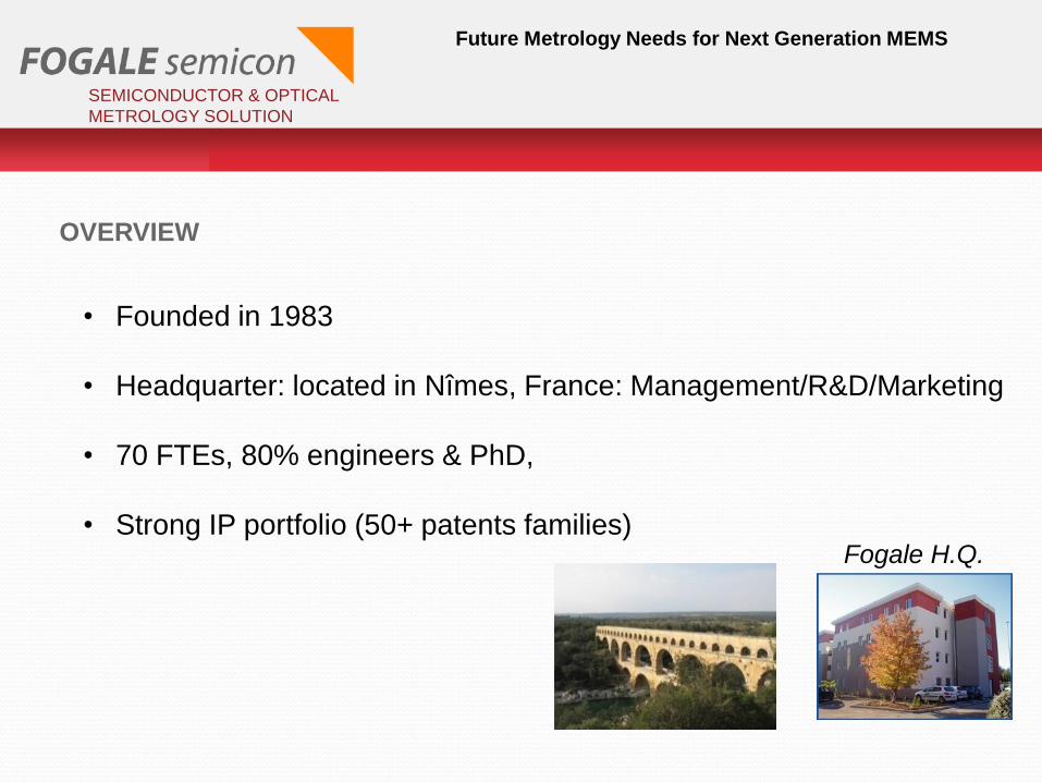
• Founded in 1983
• Headquarter: located in Nîmes, France: Management/R&D/Marketing
• 70 FTEs, 80% engineers & PhD,
• Strong IP portfolio (50+ patents families)
OVERVIEW
Fogale H.Q.
SEMICONDUCTOR & OPTICAL
METROLOGY SOLUTION
Future Metrology Needs for Next Generation MEMS
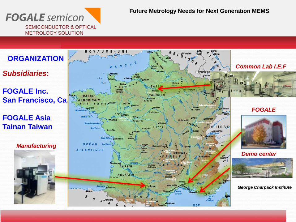
ORGANIZATION
Subsidiaries:
FOGALE Inc.
San Francisco, Ca.
FOGALE Asia
Tainan Taiwan
Manufacturing
Common Lab I.E.F
Demo center
FOGALE
George Charpack Institute
SEMICONDUCTOR & OPTICAL
METROLOGY SOLUTION
Future Metrology Needs for Next Generation MEMS
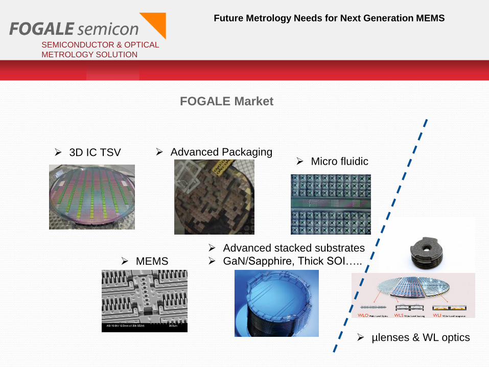
FOGALE Market
3D IC TSV
MEMS
Advanced stacked substrates
GaN/Sapphire, Thick SOI…..
Micro fluidic Advanced Packaging
µlenses & WL optics
SEMICONDUCTOR & OPTICAL
METROLOGY SOLUTION
Future Metrology Needs for Next Generation MEMS
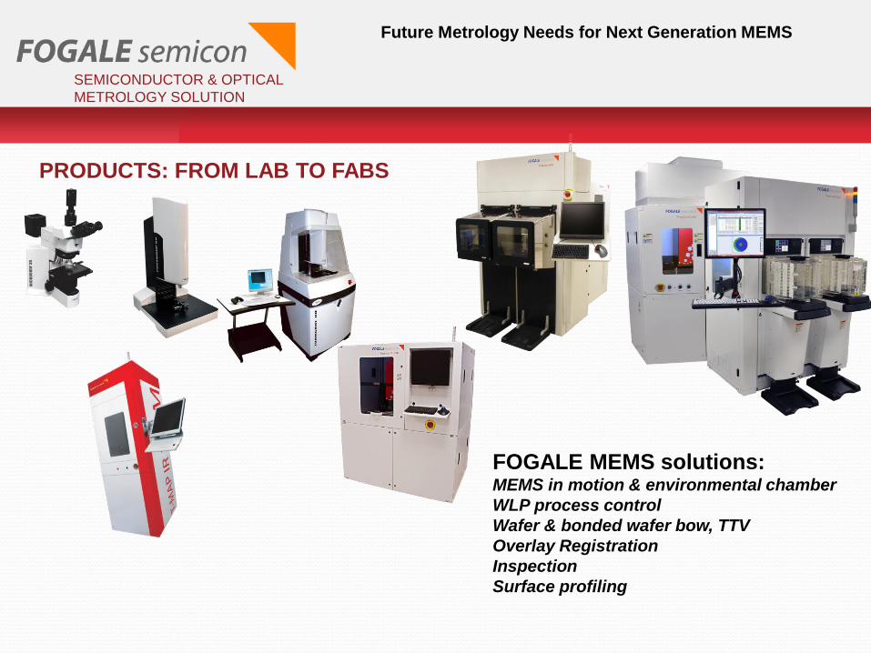
PRODUCTS: FROM LAB TO FABS
FOGALE MEMS solutions: MEMS in motion & environmental chamber
WLP process control
Wafer & bonded wafer bow, TTV
Overlay Registration
Inspection
Surface profiling
SEMICONDUCTOR & OPTICAL
METROLOGY SOLUTION
Future Metrology Needs for Next Generation MEMS
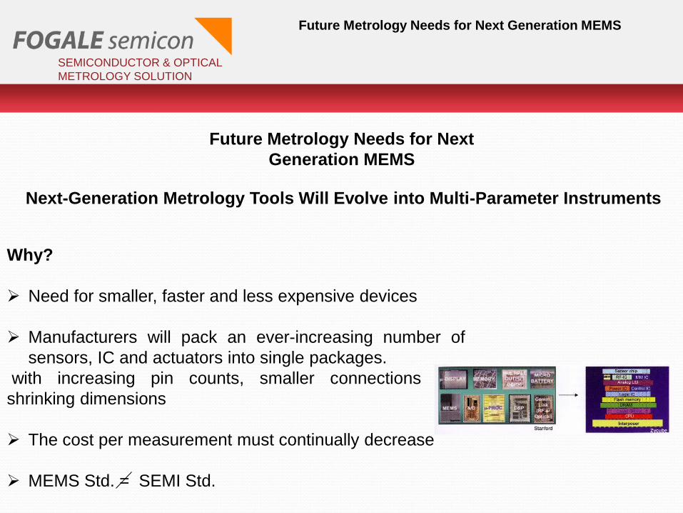
Why?
Need for smaller, faster and less expensive devices
Manufacturers will pack an ever-increasing number of
sensors, IC and actuators into single packages.
with increasing pin counts, smaller connections and
shrinking dimensions
The cost per measurement must continually decrease
MEMS Std. = SEMI Std.
Future Metrology Needs for Next
Generation MEMS
Next-Generation Metrology Tools Will Evolve into Multi-Parameter Instruments
SEMICONDUCTOR & OPTICAL
METROLOGY SOLUTION
Future Metrology Needs for Next Generation MEMS
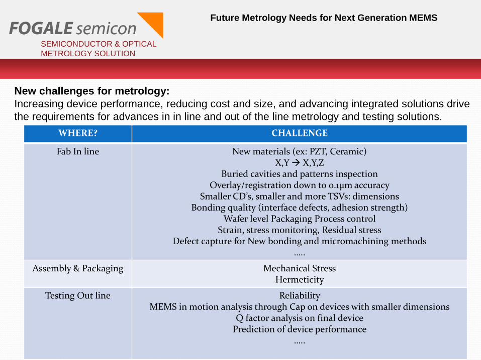
New challenges for metrology:
Increasing device performance, reducing cost and size, and advancing integrated solutions drive
the requirements for advances in in line and out of the line metrology and testing solutions.
WHERE? CHALLENGE
Fab In line New materials (ex: PZT, Ceramic) X,Y X,Y,Z
Buried cavities and patterns inspection Overlay/registration down to 0.1µm accuracy
Smaller CD’s, smaller and more TSVs: dimensions Bonding quality (interface defects, adhesion strength)
Wafer level Packaging Process control Strain, stress monitoring, Residual stress
Defect capture for New bonding and micromachining methods …..
Assembly & Packaging Mechanical Stress Hermeticity
Testing Out line Reliability MEMS in motion analysis through Cap on devices with smaller dimensions
Q factor analysis on final device Prediction of device performance
…..
SEMICONDUCTOR & OPTICAL
METROLOGY SOLUTION
Future Metrology Needs for Next Generation MEMS
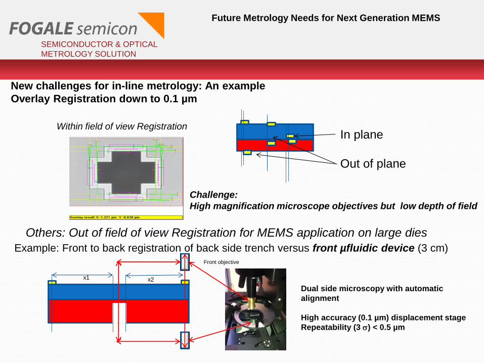
In plane
Out of plane
Others: Out of field of view Registration for MEMS application on large dies
Within field of view Registration
Example: Front to back registration of back side trench versus front µfluidic device (3 cm)
x1 x2
Dual side microscopy with automatic
alignment
High accuracy (0.1 µm) displacement stage
Repeatability (3 s) < 0.5 µm
Front objective
New challenges for in-line metrology: An example
Overlay Registration down to 0.1 µm
Challenge:
High magnification microscope objectives but low depth of field
SEMICONDUCTOR & OPTICAL
METROLOGY SOLUTION
Future Metrology Needs for Next Generation MEMS
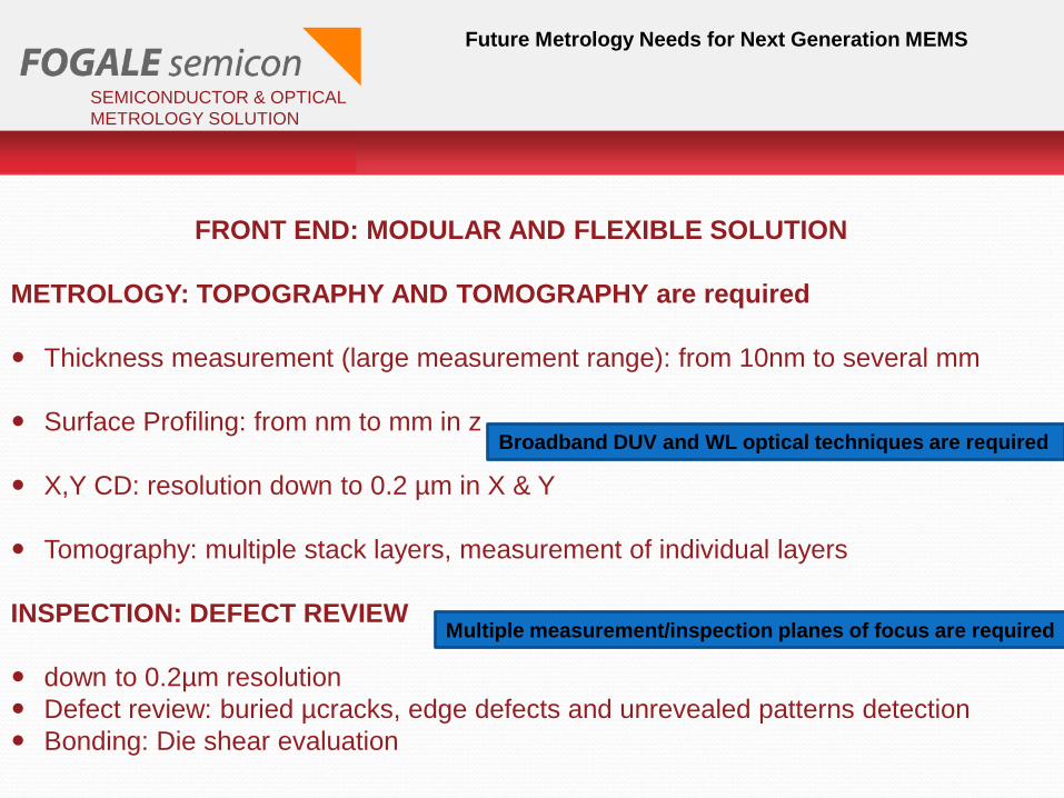
FRONT END: MODULAR AND FLEXIBLE SOLUTION
METROLOGY: TOPOGRAPHY AND TOMOGRAPHY are required
Thickness measurement (large measurement range): from 10nm to several mm
Surface Profiling: from nm to mm in z
X,Y CD: resolution down to 0.2 µm in X & Y
Tomography: multiple stack layers, measurement of individual layers
INSPECTION: DEFECT REVIEW
down to 0.2µm resolution
Defect review: buried µcracks, edge defects and unrevealed patterns detection
Bonding: Die shear evaluation
Broadband DUV and WL optical techniques are required
Multiple measurement/inspection planes of focus are required
SEMICONDUCTOR & OPTICAL
METROLOGY SOLUTION
Future Metrology Needs for Next Generation MEMS
MEMS: Silicon cooking
Specific measurement dedicated to MEMS will always be required
Tilted mirrors: Angle/roughness High NA required/sub nm level surface profiling
Micromachining: smaller devices, thinner sacrificial layers detect stiction
MEMS wafers processed on both sides: Registration/ overlay with higher accuracy
Small buried cavities: dimension measurement through Si (ex: Ink jet MEMS)
Others:
Same needs than 3D IC TSV
Via/trench dimensions, voids in metal filled TSV at Via filling, seed and diffusion
barrier conformity at the TSV sidewall ….
SEMICONDUCTOR & OPTICAL
METROLOGY SOLUTION
Future Metrology Needs for Next Generation MEMS
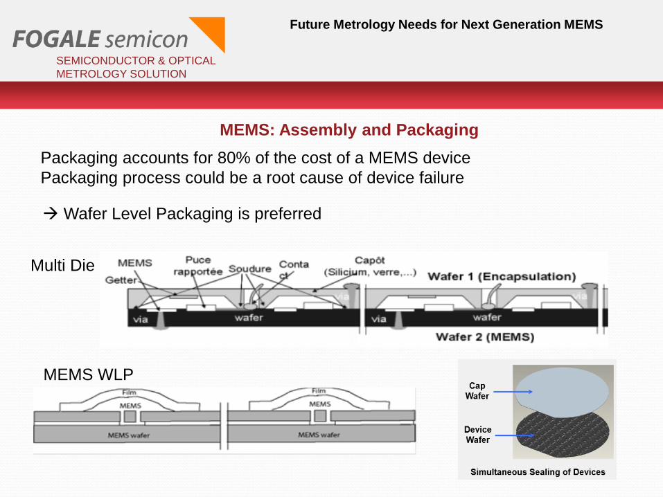
MEMS: Assembly and Packaging
Packaging accounts for 80% of the cost of a MEMS device
Packaging process could be a root cause of device failure
Wafer Level Packaging is preferred
Multi Die
MEMS WLP
SEMICONDUCTOR & OPTICAL
METROLOGY SOLUTION
Future Metrology Needs for Next Generation MEMS
Such wafer level approach will ideally require new control methods :
Electrical connection performance
Adhesion and assembly defect review
Inter die gap and constraints after stacking
Die Alignment accuracy
Device in Package MEMS in motion analysis
Hermeticity
MEMS: Assembly and Packaging
SEMICONDUCTOR & OPTICAL
METROLOGY SOLUTION
Future Metrology Needs for Next Generation MEMS
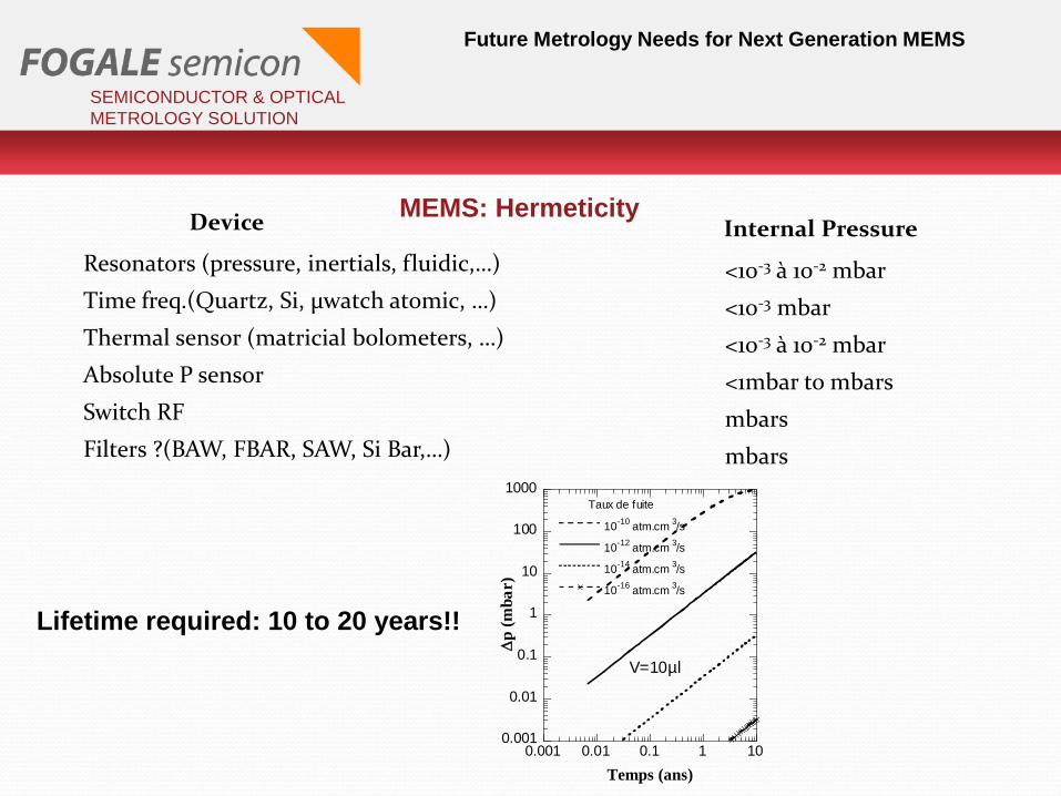
Resonators (pressure, inertials, fluidic,…)
Time freq.(Quartz, Si, µwatch atomic, …)
Thermal sensor (matricial bolometers, …)
Absolute P sensor
Switch RF
Filters ?(BAW, FBAR, SAW, Si Bar,…)
Internal Pressure
<10-3 à 10-2 mbar
<10-3 mbar
<10-3 à 10-2 mbar
<1mbar to mbars
mbars
mbars
Device MEMS: Hermeticity
Lifetime required: 10 to 20 years!!
0.001
0.01
0.1
1
10
100
1000
0.001 0.01 0.1 1 10
10-10
atm.cm3/s
10-12
atm.cm3/s
10-14
atm.cm3/s
10-16
atm.cm3/s
p
(m
ba
r)
Temps (ans)
Taux de fuite
V=10µl
SEMICONDUCTOR & OPTICAL
METROLOGY SOLUTION
Future Metrology Needs for Next Generation MEMS
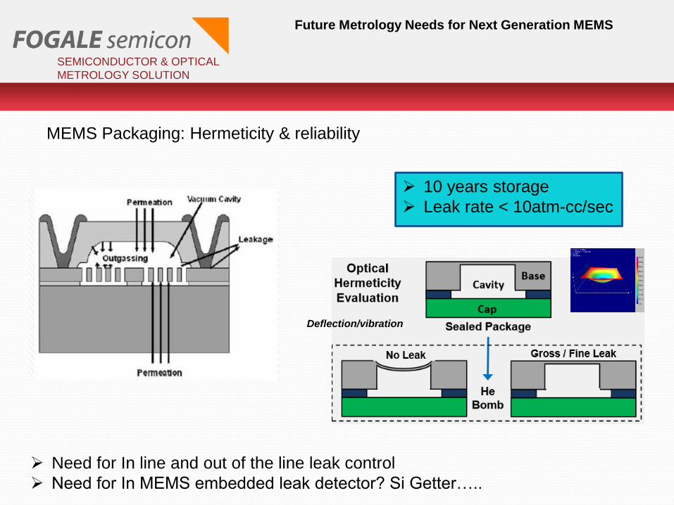
MEMS Packaging: Hermeticity & reliability
10 years storage
Leak rate < 10atm-cc/sec
Need for In line and out of the line leak control
Need for In MEMS embedded leak detector? Si Getter…..
Deflection/vibration
SEMICONDUCTOR & OPTICAL
METROLOGY SOLUTION
Future Metrology Needs for Next Generation MEMS
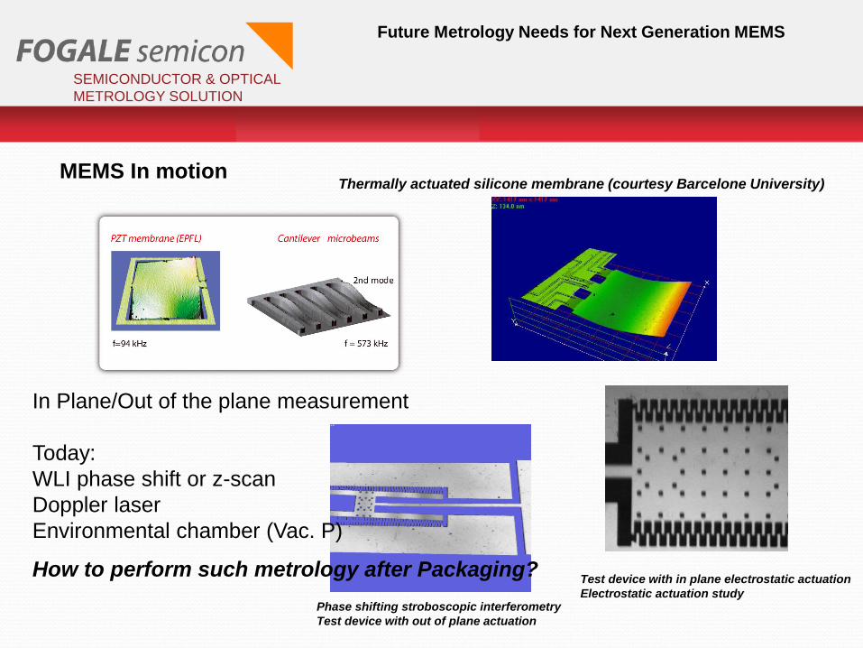
Thermally actuated silicone membrane (courtesy Barcelone University)
Phase shifting stroboscopic interferometry
Test device with out of plane actuation
Test device with in plane electrostatic actuation
Electrostatic actuation study
MEMS In motion
In Plane/Out of the plane measurement
Today:
WLI phase shift or z-scan
Doppler laser
Environmental chamber (Vac. P)
How to perform such metrology after Packaging?
SEMICONDUCTOR & OPTICAL
METROLOGY SOLUTION
Future Metrology Needs for Next Generation MEMS
MEMS In motion new requirements:
Develop IR interferometric methods
Develop full field optical methods to perform
measurement through Cap while keeping in mind
that device are becoming smaller and smaller
Out of the plane:
Interferometric objectives able to compensate cap thickness (up to 500µm?)
In plane:
Lateral resolution <<1µm
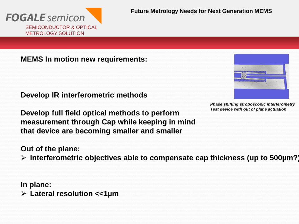
Phase shifting stroboscopic interferometry
Test device with out of plane actuation
SEMICONDUCTOR & OPTICAL
METROLOGY SOLUTION
Future Metrology Needs for Next Generation MEMS
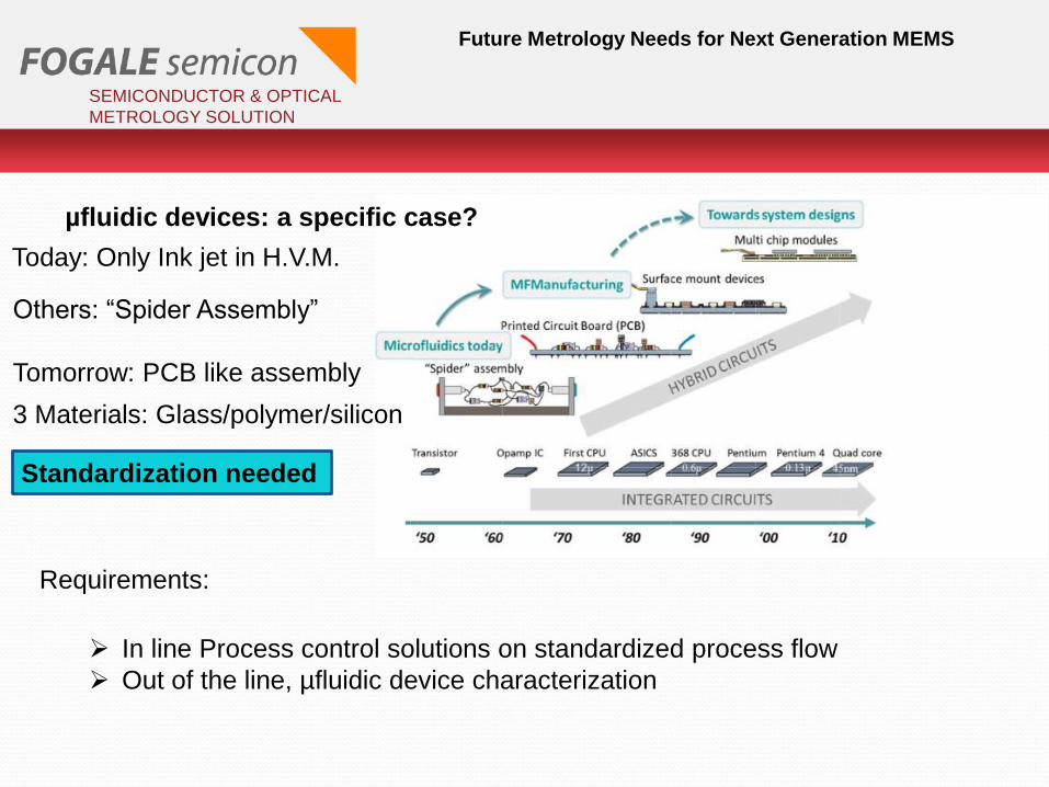
µfluidic devices: a specific case?
Others: “Spider Assembly”
Tomorrow: PCB like assembly
3 Materials: Glass/polymer/silicon
Standardization needed
Today: Only Ink jet in H.V.M.
In line Process control solutions on standardized process flow
Out of the line, µfluidic device characterization
Requirements:
SEMICONDUCTOR & OPTICAL
METROLOGY SOLUTION
Future Metrology Needs for Next Generation MEMS
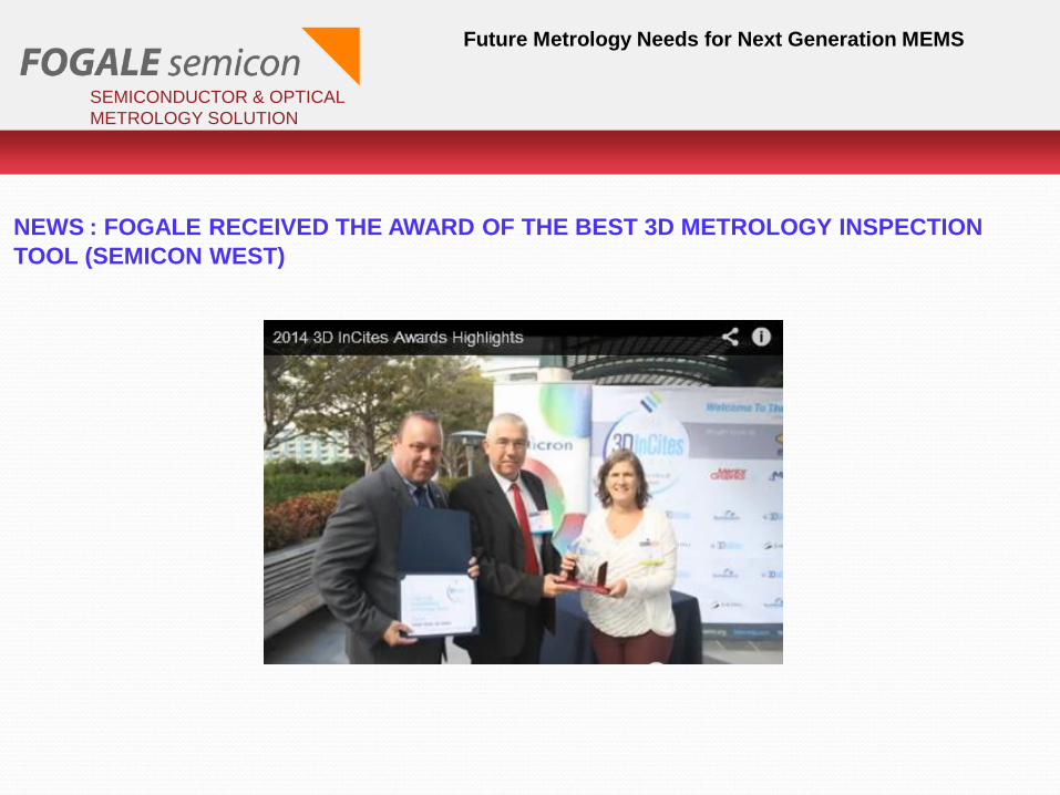
NEWS : FOGALE RECEIVED THE AWARD OF THE BEST 3D METROLOGY INSPECTION
TOOL (SEMICON WEST)
SEMICONDUCTOR & OPTICAL
METROLOGY SOLUTION
Future Metrology Needs for Next Generation MEMS
Thanks for your attention!!
Gilles FRESQUET
Semiconductor Business Dept Director
FOGALE nanotech Vice President
125 Rue de l'Hostellerie
Ville Active
BâtA-Parc Acti +
30900 NÎMES-FRANCE
Email: [email protected]
Tel: +33(0)466620555
Mobile: +33(0)684133831
Fax: +33(0)466627160
http://www.fogale-semicon.com/
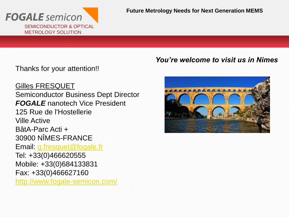
You’re welcome to visit us in Nimes