screen ic controller hx8352 - display future · hx8352-a(t) 240rgb x 480 dot ... figure 5. 8 input...
TRANSCRIPT

( DOC No. HX8352-A(T)-DS )
HX8352-A (T) 240RGB x 480 dot, 262K color, with internal GRAM, TFT Mobile Single Chip Driver Version 05 December, 2008
-P.1- Himax Confidential This information contained herein is the exclusive property of Himax and shall not be distributed, reproduced, or disclosed in whole or in part without prior written permission of Himax. December, 2008
1. General Description............................................................................................................................................. 8 2. Features ................................................................................................................................................................ 9
2.1 Display.................................................................................................................................................. 9 2.2 Display module ..................................................................................................................................... 9 2.3 Display/control interface ....................................................................................................................... 9 2.4 Miscellaneous..................................................................................................................................... 10
3. Block Diagram.................................................................................................................................................... 11 4. Pin Description................................................................................................................................................... 12
4.1 Pin description .................................................................................................................................... 12 4.2 Pin assignment ................................................................................................................................... 16 4.3 PAD coordinates................................................................................................................................. 17 4.4 Alignment mark................................................................................................................................... 25 4.5 Bump size........................................................................................................................................... 26
5. Function Description ......................................................................................................................................... 29 5.1 Interface control mode..................................................................................................................... 29
5.1.1 Register-content interface mode.............................................................................................. 30 5.1.2 Parallel bus system interface ................................................................................................... 31 5.1.3 Serial bus system interface...................................................................................................... 40 5.1.4 RGB interface........................................................................................................................... 42
5.2 Address counter (AC) ......................................................................................................................... 45 5.2.1 MCU to memory write/read direction ....................................................................................... 46
5.3 Source, gate and memory map.......................................................................................................... 48 5.4 Tearing effect output line .................................................................................................................... 49
5.4.1 Tearing effect line modes ......................................................................................................... 49 5.4.2 Tearing effect line timing........................................................................................................... 50
5.5 Oscillator............................................................................................................................................. 53 5.6 Source driver ...................................................................................................................................... 53 5.7 Gate driver.......................................................................................................................................... 53 5.8 LCD power generation circuit ............................................................................................................. 54
5.8.1 LCD power generation scheme................................................................................................ 54 5.8.2 Various boosting steps ............................................................................................................. 55
5.9 Gamma adjustment ............................................................................................................................ 56 5.9.1 Gray voltage generator for source driver ................................................................................. 57 5.9.2 Gray voltage generator for digital gamma correction............................................................... 68
5.10 Scan mode setting............................................................................................................................ 75 5.11 Register setting flow ......................................................................................................................... 76 5.12 Power supply setting ........................................................................................................................ 78 5.13 OTP programming............................................................................................................................ 79 5.14 Free running mode specification ...................................................................................................... 82
6. Command ........................................................................................................................................................... 85 6.1 Command set ..................................................................................................................................... 85 6.2 Index register .................................................................................................................................... 87 6.3 Producet ID register (R00h) ............................................................................................................. 87 6.4 Display mode control register (R01h) ............................................................................................ 87 6.5 Column address start register (R02~03h) ...................................................................................... 88 6.6 Column address end register (R04~05h) ....................................................................................... 88 6.7 Row address start register (R06~07h)............................................................................................ 88 6.8 Row address end register (R08~09h) ............................................................................................. 89 6.9 Partial area start row register (R0A~0Bh) ...................................................................................... 89 6.10 Partial area end row register (R0C~0Dh) ..................................................................................... 90 6.11 Vertical scroll top fixed area register (R0E~0Fh) ........................................................................ 91 6.12 Vertical scroll height area register (R10~11h) ............................................................................. 91 6.13 Vertical scroll button fixed area register (R12~13h) ................................................................... 91 6.14 Vertical scroll start address register (R14~15h).......................................................................... 92 6.15 Memory access control register (R16h) ....................................................................................... 94 6.16 OSC control 1 register (R17h) ....................................................................................................... 95
HX8352-A(T) 240RGB x 480 dot, 262K color, with internal GRAM, TFT Mobile Single Chip Driver
List of Contents December, 2008

-P.2- Himax Confidential
December, 2008This information contained herein is the exclusive property of Himax and shall not be distributed, reproduced, or disclosed in whole or in part without prior written permission of Himax.
6.17 OSC control 2 register (R18h) ....................................................................................................... 95 6.18 Power control 1 register (R19h) .................................................................................................... 96 6.19 Power control 2 register (R1Ah) ................................................................................................... 97 6.20 Power control 3 register (R1Bh) ................................................................................................... 98 6.21 Power control 4 register (R1Ch) ................................................................................................... 99 6.22 Power control 5 register (R1Dh) ................................................................................................. 100 6.23 Power control 6 register (R1Eh) ................................................................................................. 100 6.24 VCOM control register (R1Fh)..................................................................................................... 102 6.25 Read data register (R22h) ............................................................................................................ 104 6.26 Display control 1 register (R23h) ................................................................................................ 105 6.27 Display control 2 register (R24h) ................................................................................................ 106 6.28 Display control 3~8 register (R25h~R2Ah) ................................................................................ 107 6.29 Cycle control 1~3 register (R2B~2Dh)........................................................................................ 109 6.30 Cycle control 4~8 register (R2E~32h) .........................................................................................110 6.31 Cycle control 10 register (R34h) ..................................................................................................112 6.32 Cycle control 11 register (R35h) ..................................................................................................112 6.33 Cycle control 12 register (R36h) ..................................................................................................113 6.34 Cycle control 13~15 register (R37h~39h)....................................................................................113 6.35 Interface control 1 register (R3Ah) ..............................................................................................114 6.36 Source control 1~2 register (R3Ch~3Dh) ....................................................................................115 6.37 GAMMA control 1~12 register (R3E~49h) ...................................................................................116 6.38 Panel control register (R55h) .......................................................................................................119 6.39 OTP related register 1 (R56h) .......................................................................................................119 6.40 OTP related register 2 (R57h) ...................................................................................................... 120 6.41 OTP related register 3 (R58h) ...................................................................................................... 120 6.42 OTP related register 4 (R59h) ...................................................................................................... 120 6.43 IP control register (R5Ah) ............................................................................................................ 121 6.44 DGC LUT register (R5Ch) ............................................................................................................ 121 6.45 Test mode control register (R83h) .............................................................................................. 122 6.46 VDDD control register (R85h)...................................................................................................... 122 6.47 Power driving control register (R8Ah) ....................................................................................... 123 6.48 Source gamma resistor setting register (R8B~R8Ch) .............................................................. 123 6.49 SYNC function register (R91h).................................................................................................... 124 6.50 PWM control 1 register (R95h) .................................................................................................... 124 6.51 PWM control 2 register (R96h) .................................................................................................... 124 6.52 PWM control 3 register (R97h) .................................................................................................... 125 6.53 CABC PWM period control 1 register (R6Bh) ............................................................................ 126 6.54 CABC PWM period control 2 register (R6Ch) ............................................................................ 126 6.55 CABC gain setting register (R6Fh ~ R77h) ................................................................................ 126
7. Electrical Characteristic .................................................................................................................................. 128 7.1 Absolute maximum ratings ........................................................................................................... 128 7.2 ESD protection level ...................................................................................................................... 128 7.3 Latch-up protection level............................................................................................................... 128 7.4 Light sensitivity .............................................................................................................................. 128 7.5 Maximum series resistance........................................................................................................... 129 7.6 DC characteristics .......................................................................................................................... 130 7.7 AC characteristics .......................................................................................................................... 131
7.7.1 Parallel interface characteristics (8080-series MPU)............................................................. 131 7.7.2 Parallel interface characteristics (6800-series MPU)............................................................. 133 7.7.3 Serial interface characteristics ............................................................................................... 134 7.7.4 RGB interface characteristics................................................................................................. 135 7.7.5 Reset input timing .................................................................................................................. 137
8. Reference Applications ................................................................................................................................... 138 8.1 Register- content interface mode ................................................................................................. 138
HX8352-A(T) 240RGB x 480 dot, 262K color, with internal GRAM, TFT Mobile Single Chip Driver
List of Contents December, 2008

-P.3- Himax Confidential
December, 2008This information contained herein is the exclusive property of Himax and shall not be distributed, reproduced, or disclosed in whole or in part without prior written permission of Himax.
8.2 External components connection................................................................................................. 139
9. Ordering Information ....................................................................................................................................... 140 10. Revision History............................................................................................................................................. 140
HX8352-A(T) 240RGB x 480 dot, 262K color, with internal GRAM, TFT Mobile Single Chip Driver
List of Contents December, 2008
-P.4- Himax Confidential
December, 2008This information contained herein is the exclusive property of Himax and shall not be distributed, reproduced, or disclosed in whole or in part without prior written permission of Himax.
Figure 5. 1 Register Read/Write Timing in Parallel Bus System Interface (for I80 Series MPU)...... 31 Figure 5. 2 GRAM Read/Write Timing in 16-/18-Bit Parallel Bus System Interface (for I80 Series
MPU) .......................................................................................................................................... 32 Figure 5. 3 GRAM Read/Write Timing in 8-Bit Parallel Bus System Interface (for I80 Series MPU) 33 Figure 5. 4 Register Read/Write Timing in Parallel Bus System Interface (for M68 Series MPU).... 34 Figure 5. 5 GRAM Read/Write Timing in 16-/18-Bit Parallel Bus System Interface (for M68 Series
MPU) .......................................................................................................................................... 35 Figure 5. 6 GRAM Read/Write Timing in 8-bit Parallel Bus System Interface (for M68 Series MPU)
................................................................................................................................................... 36 Figure 5. 7 Example of I80- / M68- System 16-Bit Parallel Bus Interface......................................... 37 Figure 5. 8 Input Data Bus and GRAM Data Mapping in 18-Bit Bus System Interface
(“BS2, BS1, BS0”=”010”) ........................................................................................................... 37 Figure 5. 9 Example of I80- / M68- System 16-bit Parallel Bus Interface......................................... 38 Figure 5. 10 Input Data Bus and GRAM Data Mapping in 16-Bit Bus System Interface with 16
Bit-Data Input (“BS2, BS1, BS0”=”000”) .................................................................................... 38 Figure 5. 11 Input Data Bus and GRAM Data Mapping in 16-Bit Bus System Interface with 18(16+2)
Bit-Data Input (“BS2, BS1, BS0”=”001”) .................................................................................... 38 Figure 5. 12 Example of I80- / M68- System 8-Bit Parallel Bus Interface......................................... 39 Figure 5. 13 Input Data Bus and GRAM Data Mapping in 8-Bit Bus System Interface with 18( 6 + 6 +
6 ) Bit-Data Input (“BS2, BS1, BS0”=”011”) ............................................................................... 39 Figure 5. 14 Input Data Bus and GRAM Data Mapping in 8-Bit Bus System Interface with 16(5 + 6 +
5) Bit-Data Input (“BS2, BS1, BS0”=”100”) ................................................................................ 39 Figure 5. 15 Data Write Timing in Serial Bus System Interface........................................................ 41 Figure 5. 16 Data Write Timing in Serial Bus System Interface........................................................ 41 Figure 5. 17 RGB Interface Circuit Input Timing ............................................................................... 42 Figure 5. 18 16-Bit / Pixel Data Input of RGB Interface .................................................................... 43 Figure 5. 19 18-Bit / Pixel Data Input of RGB Interface .................................................................... 44 Figure 5. 20 MCU to Memory Write/Read Direction ......................................................................... 46 Figure 5. 21 MY, MX, MV Setting of 240RGB x 432 Dot .................................................................. 46 Figure 5. 22 Address Direction Settings............................................................................................ 47 Figure 5. 23 Memory Map (240RGBx432) ........................................................................................ 48 Figure 5. 24 TE Mode 1 Output......................................................................................................... 49 Figure 5. 25 TE Mode 2 Output......................................................................................................... 49 Figure 5. 26 TE Output Waveform .................................................................................................... 49 Figure 5. 27 Tearing Effect Signal Output......................................................................................... 50 Figure 5. 28 AC Characteristics of Tearing Effect Signal.................................................................. 50 Figure 5. 29 ....................................................................................................................................... 51 Figure 5. 30 ....................................................................................................................................... 51 Figure 5. 31 ....................................................................................................................................... 52 Figure 5. 32 ....................................................................................................................................... 52 Figure 5. 33 Oscillation Circuit .......................................................................................................... 53 Figure 5. 34 LCD Power Generation Scheme .................................................................................. 54 Figure 5. 35 Various Boosting Steps................................................................................................. 55 Figure 5. 36 Gamma Adjustments Different of Source Driver with Digital Gamma Correction......... 56 Figure 5. 37 Grayscale Control ......................................................................................................... 57 Figure 5. 38 Structure of Grayscale Voltage Generator .................................................................... 58 Figure 5. 39 Gamma Resister Stream and Gamma Reference Voltage .......................................... 61 Figure 5. 40 Relationship between Source Output and Vcom.......................................................... 67 Figure 5. 41 Relationships between GRAM Data and Output Level................................................. 67 Figure 5. 42 Block Diagram of Digital Gamma Correction................................................................ 68 Figure 5. 43 Scan Function (240RGB x 432 Dot) ............................................................................. 75 Figure 5. 44 Display On/Off Set Sequence....................................................................................... 76 Figure 5. 45 Standby Mode Setting Sequence ................................................................................. 77 Figure 5. 46 Power Supply Setting Flow........................................................................................... 78 Figure 5. 47 OTP Programming Flow ............................................................................................... 80 Figure 5. 48 Power On Sequence of FR-mode (for Normally–White Panel) .................................... 83
HX8352-A (T) 240RGB x 480 dot, 262K color, with internal GRAM, TFT Mobile Single Chip Driver List of Figures December, 2008

-P.5- Himax Confidential
December, 2008This information contained herein is the exclusive property of Himax and shall not be distributed, reproduced, or disclosed in whole or in part without prior written permission of Himax.
Figure 5. 49 Power Off Sequence of FR-mode................................................................................. 83
Figure 6. 1 Index Register................................................................................................................. 87 Figure 6. 2 Product ID Register (R00h) ............................................................................................ 87 Figure 6. 3 Display Mode Control Register (R01h) ........................................................................... 87 Figure 6. 4 Column Address Start Register Upper Byte (R02h) ....................................................... 88 Figure 6. 5 Column Address Start Register Low Byte (R03h) .......................................................... 88 Figure 6. 6 Column Address End Register Upper Byte (R04h) ........................................................ 88 Figure 6. 7 Column Address End Register Low Byte (R05h) ........................................................... 88 Figure 6. 8 Row Address Start Register Upper Byte (R06h) ............................................................ 88 Figure 6. 9 Row Address Start Register Low Byte (R07h)................................................................ 88 Figure 6. 10 Row Address End Register Upper Byte (R08h) ........................................................... 89 Figure 6. 11 Row Address End Register Low Byte (R09h) ............................................................... 89 Figure 6. 12 Partial Area Start Row Register Upper Byte (R0Ah) .................................................... 89 Figure 6. 13 Partial Area Start Row Register Low Byte (R0Bh) ....................................................... 89 Figure 6. 14 Partial Area End Row Register Upper Byte (R0Ch) ..................................................... 90 Figure 6. 15 Partial Area End Row Register Low Byte (R0Dh) ........................................................ 90 Figure 6. 16 Vertical Scroll Top Fixed Area Register Upper Byte (R0Eh) ........................................ 91 Figure 6. 17 Vertical Scroll Top Fixed Area Register Low Byte (R0Fh)............................................ 91 Figure 6. 18 Vertical Scroll Height Area Register Upper Byte (R10h) .............................................. 91 Figure 6. 19 Vertical Scroll Height Area Register Low Byte (R11h) ................................................. 91 Figure 6. 20 Vertical Scroll Button Fixed Area Register Upper Byte (R12h) .................................... 91 Figure 6. 21 Vertical Scroll Button Fixed Area Register Low Byte (R13h)........................................ 91 Figure 6. 22 Vertical Scroll Start Address Register Upper Byte (R14h) ........................................... 92 Figure 6. 23 Vertical Scroll Start Address Register Low Byte (R15h)............................................... 92 Figure 6. 24 Memory Access Control Register (R16h) ..................................................................... 94 Figure 6. 25 OSC Control 1 Register (R17h) .................................................................................... 95 Figure 6. 26 OSC Control 2 Register (R18h) .................................................................................... 95 Figure 6. 27 Power Control 1 Register (R19h).................................................................................. 96 Figure 6. 28 Power Control 2 Register (R1Ah) ................................................................................. 97 Figure 6. 29 Power Control 3 Register (R1Bh) ................................................................................. 98 Figure 6. 30 Power Control 4 Register (R1Ch) ................................................................................. 99 Figure 6. 31 Power Control 5 Register (R1Dh) ............................................................................... 100 Figure 6. 32 Power Control 6 Register (R1Eh) ............................................................................... 100 Figure 6. 33 VCOM Control Register (R1Fh).................................................................................. 102 Figure 6. 34 Read Data Register (R22h) ........................................................................................ 104 Figure 6. 35 Write Data Register (R22h) ........................................................................................ 104 Figure 6. 36 Display Control Register (R23h) ................................................................................. 105 Figure 6. 37 Display Control 2 Register (R24h) .............................................................................. 106 Figure 6. 38 Display Control 2 Register (R25h) .............................................................................. 107 Figure 6. 39 Display Control 3 Register (R26h) .............................................................................. 107 Figure 6. 40 Display Control 4 Register (R27h) .............................................................................. 107 Figure 6. 41 Display Control 5 Register (R28h) .............................................................................. 107 Figure 6. 42 Display Control 6 Register (R29h) .............................................................................. 107 Figure 6. 43 Display Control 7 Register (R2Ah).............................................................................. 107 Figure 6. 44 Cycle Control 1 Register (R2Bh) ................................................................................ 109 Figure 6. 45 Cycle Control 2 Register (R2Ch) ................................................................................ 109 Figure 6. 46 Cycle Control 3 Register (R2Dh) ................................................................................ 109 Figure 6. 47 Cycle Control 4 Register (R2Eh) .................................................................................110 Figure 6. 48 Cycle Control 5 Register (R2Fh)..................................................................................110 Figure 6. 49 Cycle Control 1 Register (R30h)..................................................................................110 Figure 6. 50 Cycle Control 2 Register (R31h)..................................................................................110 Figure 6. 51 Cycle Control 3 Register (R32h)..................................................................................110 Figure 6. 52 Cycle Control 10 Register (R34h)................................................................................112 Figure 6. 53 Cycle Control 11 Register (R35h)................................................................................112
HX8352-A (T) 240RGB x 480 dot, 262K color, with internal GRAM, TFT Mobile Single Chip Driver List of Figures December, 2008

-P.6- Himax Confidential
December, 2008This information contained herein is the exclusive property of Himax and shall not be distributed, reproduced, or disclosed in whole or in part without prior written permission of Himax.
Figure 6. 54 Cycle Control 12 Register (R36h)................................................................................113 Figure 6. 55 Display Control 5 Register (R37h) ...............................................................................113 Figure 6. 56 Display Control 6 Register (R38h) ...............................................................................113 Figure 6. 57 Display Control 3 Register (R39h) ...............................................................................114 Figure 6. 58 Interface Control 1 Register (R3Ah) ............................................................................114 Figure 6. 59 Source Control 1 Register (R3Ch)...............................................................................115 Figure 6. 60 Source Control 2 Register (R3Dh)...............................................................................115 Figure 6. 61 GAMMA Control 1 Register (R3Eh).............................................................................116 Figure 6. 62 GAMMA Control 2 Register (R3Fh) .............................................................................116 Figure 6. 63 GAMMA Control 3 Register (R40h) .............................................................................116 Figure 6. 64 GAMMA Control 4 Register (R41h) .............................................................................116 Figure 6. 65 GAMMA Control 5 Register (R42h) .............................................................................116 Figure 6. 66 GAMMA Control 6 Register (R43h) .............................................................................117 Figure 6. 67 GAMMA Control 7 Register (R44h) .............................................................................117 Figure 6. 68 GAMMA Control8 Register (R45h) ..............................................................................117 Figure 6. 69 GAMMA Control 9 Register (R46h) .............................................................................117 Figure 6. 70 GAMMA Control 10 Register (R47h) ...........................................................................117 Figure 6. 71 GAMMA Control 11 Register (R48h) ...........................................................................117 Figure 6. 72 GAMMA Control 12 Register (R49h) ...........................................................................117 Figure 6. 73 Panel Control Register (R55h).....................................................................................119 Figure 6. 74 OTP Related Register 1 (R56h)...................................................................................119 Figure 6. 75 OTP Related Register 1 (R57h).................................................................................. 120 Figure 6. 76 OTP Related Register 3 (R58h).................................................................................. 120 Figure 6. 77 OTP Related Register 4 (R59h).................................................................................. 120 Figure 6. 78 IP Control Register (R5Ah) ......................................................................................... 121 Figure 6. 79 DGC LUT WRITE Register (R5Ch) ............................................................................ 121 Figure 6. 80 TEST MODE Control Register (R83h) ........................................................................ 122 Figure 6. 81 VDDD Control Register (R85h)................................................................................... 122 Figure 6. 82 Power driving control register (R8Ah)......................................................................... 123 Figure 6. 83 Serial Bus Interface Control Register (R8Bh) ............................................................. 123 Figure 6. 84 Serial Bus Interface Control Register (R8Ch)............................................................. 123 Figure 6. 85 SYNC Function Register (R91h)................................................................................. 124 Figure 6. 86 PWM Control 1 Register (R95h) ................................................................................. 124 Figure 6. 87 PWM Control 2 Register (R96h) ................................................................................. 124 Figure 6. 88 CABC PWM Period Control 1 Register (R6Bh) .......................................................... 125 Figure 6. 89 CABC PWM Period Control 2 Register (R6Ch) .......................................................... 125 Figure 6. 90 CABC Gain setting Register (R6Fh) ........................................................................... 126 Figure 6. 91 CABC Gain setting Register (R70h) ........................................................................... 126 Figure 6. 92 CABC Gain setting Register (R71h) ........................................................................... 126 Figure 6. 93 CABC Gain setting Register (R72h) ........................................................................... 126 Figure 6. 94 CABC Gain setting Register (R73h) ........................................................................... 126 Figure 6. 95 CABC Gain setting Register (R74h) ........................................................................... 126 Figure 6. 96 CABC Gain setting Register (R75h) ........................................................................... 126 Figure 6. 97 CABC Gain setting Register (R76h) ........................................................................... 127 Figure 6. 98 CABC Gain setting Register (R77h) ........................................................................... 127
Figure 7. 1 Parallel Interface Characteristics (8080-series MPU)................................................... 131 Figure 7. 2 Chip Select Timing........................................................................................................ 132 Figure 7. 3 Write to Read and Read to Write Timing...................................................................... 132 Figure 7. 4 Parallel Interface Characteristics (6800-series MPU)................................................... 133 Figure 7. 5 Serial Interface Characteristics..................................................................................... 134 Figure 7. 6 RGB Interface Characteristics ...................................................................................... 135 Figure 7. 7 Reset Input Timing........................................................................................................ 137
HX8352-A (T) 240RGB x 480 dot, 262K color, with internal GRAM, TFT Mobile Single Chip Driver List of Figures December, 2008

-P.7- Himax Confidential
December, 2008This information contained herein is the exclusive property of Himax and shall not be distributed, reproduced, or disclosed in whole or in part without prior written permission of Himax.
Table 5. 1 Interface Mode Selection.................................................................................................. 29 Table 5. 2 MPU selection in Register-content Interface Circuit......................................................... 30 Table 5. 3 Interface Selection in Register-content Interface Mode ................................................... 30 Table 5. 4 Data Pin Function for I80 Series CPU.............................................................................. 31 Table 5. 5 Data Pin Function for M68 Series CPU............................................................................ 31 Table 5. 6 The Function of RS and R/W Bit bus ............................................................................... 40 Table 5. 7 EPL Bit Setting and Valid Enable Signal .......................................................................... 42 Table 5. 8 Addresses Counter Range ............................................................................................... 45 Table 5. 9 MY, MX, MV Setting of 240RGB x 432 Dot...................................................................... 46 Table 5. 10 AC Characteristics of Tearing Effect Signal ................................................................... 50 Table 5. 11 Gamma-Adjustment Registers........................................................................................ 59 Table 5. 12 Offset Adjustment 0 ........................................................................................................ 62 Table 5. 13 Offset Adjustment 1 ........................................................................................................ 62 Table 5. 14 Center Adjustment.......................................................................................................... 62 Table 5. 15 Output Voltage of 8 to 1 Selector ................................................................................... 62 Table 5. 16 Voltage Calculation Formula (Positive Polarity) ............................................................. 63 Table 5. 17 Voltage Calculation Formula of Grayscale Voltage (Positive Polarity) .......................... 64 Table 5. 18 Voltage Calculation Formula (Negative Polarity) ........................................................... 65 Table 5. 19 Voltage Calculation Formula of Grayscale Voltage (Negative Polarity) ......................... 66 Table 5. 20 LUT for Red Color (1) ..................................................................................................... 69 Table 5. 21 LUT for Red Color (2) ..................................................................................................... 70 Table 5. 22 LUT for Green Color (1).................................................................................................. 71 Table 5. 23 LUT for Green Color (2).................................................................................................. 72 Table 5. 24 LUT for Blue Color (1) .................................................................................................... 73 Table 5. 25 LUT for Blue Color (2) .................................................................................................... 74 Table 5. 26 OTP Memory Table......................................................................................................... 79 Table 5. 27 Pin Information of Free Running Mode .......................................................................... 82 Table 5. 28 Frequency Definition of Free Running Mode Display..................................................... 84
Table 7. 1 ESD Protection Level ..................................................................................................... 128 Table 7. 2......................................................................................................................................... 129 Table 7. 3 DC Characteristic ........................................................................................................... 130 Table 7. 4 RGB Interface Characteristics........................................................................................ 135 Table 7. 5 Vertical and Horizontal Timing for RGB I/F................................................................... 1375 Table 7. 6 Reset Input Timing ......................................................................................................... 137
Table 8. 1 Connect Capacitors ........................................................................................................ 139 Table 8. 2 Connected Schottky Diode and Resistor........................................................................ 139
HX8352-A(T) 240RGB x 480 dot, 262K color, with internal GRAM, TFT Mobile Single Chip Driver List of Table December, 2008
-P.8- Himax Confidential This information contained herein is the exclusive property of Himax and shall not be distributed, reproduced, or disclosed in whole or in part without prior written permission of Himax. December, 2008
1. General Description This document describes Himax’s HX8352-A is supports four types resolution driving controller. The HX8352-A is designed to provide a single-chip solution that combines a gate driver, a source driver, power supply circuit for 262,144 colors to drive a TFT panel with 240RGBx480 dots at maximum. The HX8352-A can be operated in low-voltage (1.65V) condition for the interface and integrated internal boosters that produce the liquid crystal voltage, breeder resistance and the voltage follower circuit for liquid crystal driver. In addition, the HX8352-A also supports various functions to reduce the power consumption of a LCD system via software control. The HX8352-A is suitable for any small portable battery-driven and long-term driving products, such as small PDAs, digital cellular phones and bi-directional pagers. The HX8352-A supports three interface modes, includ Command-Parameter interface mode, Register-Content interface mode. The interface mode is selected by the external pins IFSEL0, P68, BS2~0 setting.
HX8352-A (T) 240RGB x 480 dot, 262K color, with internal GRAM, TFT Mobile Single Chip Driver Version 05 December, 2008

-P.9- Himax Confidential
December, 2008This information contained herein is the exclusive property of Himax and shall not be distributed, reproduced, or disclosed in whole or in part without prior written permission of Himax.
HX8352-A(T) 240RGB x 480 dot, 262K color, TFT Mobile Single Chip Driver
DATA SHEET V05
2. Features 2.1 Display
Resolution 240(H) x RGB(H) x 480(V) 240(H) x RGB(H) x 432(V) 240(H) x RGB(H) x 400(V) 240(H) x RGB(H) x 320(V)
Display Color modes Normal Display Mode On
− 65,536(R(5),G(6),B(5)) colors − 262,144(R(6),G(6),B(6)) colors
Idle Mode On
− 8 (R(1), G(1), B(1)) colors.
2.2 Display module
On module VCOM control (-2.0 to 5.5V Common electrode output voltage range) On module DC/DC converter
VLCD = 4.6 to 6.0V (Source output voltage range) VGH = +9.0 to +16.5V (Positive Gate output voltage range) VGL = -6.0 to -13.5V (Negative Gate output voltage range)
Frame Memory area 240 (H) x 480 (V) x 18 bit 2.3 Display/control interface
Display Interface types supported 8-/16-/18-bit MPU parallel interface. Serial data transfer interface. 16-/18-data lines parallel video (RGB) interface.
Control Interface types supported Register-Content interface mode.
Logic voltage (IOVCC): 1.65 ~ 3.3V Logic voltage (VCC): 2.3 ~ 3.3V Driver power supply (VCI): 2.3 ~ 3.3V Color modes
16 bit/pixel: R(5), G(6), B(5) 18 bit/pixel: R(6), G(6), B(6)
-P.10- Himax Confidential
December, 2008This information contained herein is the exclusive property of Himax and shall not be distributed, reproduced, or disclosed in whole or in part without prior written permission of Himax.
HX8352-A(T) 240RGB x 480 dot, 262K color, TFT Mobile Single Chip Driver
DATA SHEET V052.4 Miscellaneous
Low power consumption, suitable for battery operated systems Image sticking eliminated function CMOS compatible inputs Optimized layout for COG assembly Temperature range: -40 ~ +85 °C Proprietary multi phase driving for lower power consumption Support external VDD for lower power consumption (such as 1.8 volts input) Support RGB through mode with lower power consumption Support Gamma correction of RGB independence Support normal black/normal white LCD Support wide view angle display Support burn-in mode for efficient test in module production On-chip OTP (one-time-programming) non-volatile memory

-P.11- Himax Confidential
December, 2008This information contained herein is the exclusive property of Himax and shall not be distributed, reproduced, or disclosed in whole or in part without prior written permission of Himax.
HX8352-A(T) 240RGB x 480 dot, 262K color, TFT Mobile Single Chip Driver
DATA SHEET V05
3. Block Diagram

-P.12- Himax Confidential
December, 2008This information contained herein is the exclusive property of Himax and shall not be distributed, reproduced, or disclosed in whole or in part without prior written permission of Himax.
HX8352-A(T) 240RGB x 480 dot, 262K color, TFT Mobile Single Chip Driver
DATA SHEET V05
4. Pin Description 4.1 Pin description
Input Parts
Signals I/O Pin Number
Connected with Description
Select the MPU interface mode as listed below Use with IFSEL0=1 Register-content interface mode. P68 BS2 BS1 BS0 Interface mode DB pins
0 0 0 0 16-bit bus interface, 80-system, 65K-Color
D17-D16: Unused, D15-D0: Data
0 0 0 1 16-bit bus interface, 80-system, 262K-color
D17-D16: Unused, D15-D0: Data
0 0 1 0 18-bit bus interface, 80-system, 262K-color D17-D0: Data
0 0 1 1 8-bit bus interface, 80-system, 262K-Color
D17-D8: Unused D7-D0: Data
0 1 0 0 8-bit bus interface, 80-system, 65K-Color
D17-D8: Unused D7-D0: Data
1 0 0 0 16-bit bus interface, 68-system, 65K-Color
D17-D16: Unused, D15-D0: Data
1 0 0 1 16-bit bus interface, 68-system, 262K-color
D17-D16: Unused, D15-D0: Data
1 0 1 0 18-bit bus interface, 68-system, 262K-Color D17-D0: Data
1 0 1 1 8-bit bus interface, 68-system, 262K-color
D17-D8:Unused D7-D0: Data
1 1 0 0 8-bit bus interface, 68-system, 65K-color
D17-D8:Unused D7-D0: Data
P68, BS2,BS1,BS0 I 4 VSSD/ IOVCC
X 1 1 ID Serial bus IF + RGB interface
DNC_SCL, SDO,SDI, VSYNC, HSYNC, ENABLE, DOTCLK, DB17-0
IFSEL0 I 1 MPU
Interface format select pin IFSEL0 Interface Format Selection
0 Command-Parameter interface mode 1 Register-content interface mode
In this case, the IFSEL0 has to be connected to IOVCC.
EXTC I 1 MPU When operate in Register-content interface mode, the EXTC has to be connected to IOVCC or VSSD.
RES_SEL1~0 I 2 MPU
Panel Resolution select pin. RES_SEL1 RES_SEL0 Panel Resolution Connection of
Gate 0 0 240RGB x 320 dot G1 ~ G320 0 1 240RGB x 400 dot G1 ~ G400 1 0 240RGB x 432 dot G1 ~ G432 1 1 240RGB x 480 dot G1 ~ G480
NCS I 1 MPU
Chip select signal. Low: chip can be accessed; High: chip cannot be accessed. Must be connected to VSSD if not in use.
NWR_RNW I 1 MPU I80 system: Serves as a write signal and writes data at the rising edge.M68 system: 0: Write, 1: Read. Fix it to IOVCC or VSSD level when using serial bus interface.
NRD_E I 1 MPU I80 system: Serves as a read signal and read data at the low level. M68 system: 0: Read/Write disable, 1: Read/Write enable. Fix it to IOVCC or VSSD level when using serial bus interface.
DNC_SCL I 1 MPU
The signal for command or parameter select under parallel mode(i.e. Not serial interface): Low: command, High: parameter. When under serial interface, it servers as SCL.
BURN I 1 MPU Free Running mode If BURN=Hi, this can enable free running mode for burn in test. The display data alternates between full black and full white independent of input data in free running mode.
SDI I 1 MPU Serial data input. If not used, please let it connected to IOVCC or VSSD.

-P.13- Himax Confidential
December, 2008This information contained herein is the exclusive property of Himax and shall not be distributed, reproduced, or disclosed in whole or in part without prior written permission of Himax.
HX8352-A(T) 240RGB x 480 dot, 262K color, TFT Mobile Single Chip Driver
DATA SHEET V05
Input Parts
Signals I/O Pin Number
Connected with Description
VSYNC I 1 MPU Frame synchronizing signal. Has to be fixed to IOVCC level if is not used.
HSYNC I 1 MPU Frame synchronizing signal. Has to be fixed to IOVCC level if is not used.
ENABLE I 1 MPU A data ENABLE signal in RGB I/F mode. Has to be fixed to VSSD level if unused (High active, if EPL=0).
DOTCLK I 1 MPU Dot clock signal. Has to be fixed to VSSD level if is not used.
NRESET I 8 MPU or reset circuit
Reset pin. Setting either pin low initializes the LSI. Must be reset after power is supplied.
OSC I 1 Oscillation Resistor
Oscillator input for test purpose. If not used, please let it open or connected to VSSD.
VCOMR I 2 Resistor or open
A VcomH reference voltage. When adjusting VcomH externally, set registers to halt the VcomH internal adjusting circuit and place a variable resistor between VREG1 and VSSD. Otherwise, leave this pin open and adjust VcomH by setting the internal register of the HX8352-A.
VGS I 2 VSSD or external resistor
Connect to a variable resistor to adjusting internal gamma reference voltage for matching the characteristic of different panel used.
Output Part
Signals I/O Pin Number
Connected with Description
S1~S720 O 720 LCD Output voltages applied to the liquid crystal.
G1~G480 O 480 LCD Gate driver output pins. These pins output VGH, VGL.(If not used, should be open)
VCOM O 7 TFT
common electrode
The power supply of common voltage in TFT driving. The voltage amplitude between VCOMH and VCOML is output. Connect this pin to the common electrode in TFT panel.
TE O 2 MPU Tearing effect output. If not used, please open this pin. SDO O 2 MPU Serial data output. If not use, let it to open.
NISD O 2 Open Image Sticking Discharge signal. This pin is used for monitoring image sticking discharge phenomena. When the NISD goes low, the VGL, Source and VCOM would be discharged to VSSA. When the NISD goes high, the VGL, Source and VCOM are normal operation.
PWM_OUT O 2 External LED driver IC
Backlight On/Off control pin. If use ABC function, the pin can connect to external LED driver IC. The output voltage rage = 0~ IOVCC.
NWR2 O 2 Sub Panel 80-interface NWR signal output pin for Sub Panel E2 O 2 Sub Panel 68-interface Enable signal output pin for Sub Panel
NCS2 O 2 Sub Panel The signal is Chip select for Sub Panel. RS2 O 2 Sub Panel The signal is register index or register parameter select for Sub Panel
HSIM Interface Parts
Signals I/O Pin Number
Connected with Description
STB+, STB- - 2
2 HSIM HostHigh Speed Interface Strobe differential signal input pins. STB+ pin for Strobe+, STB- pin for Strobe-. Connect to a terminal resistance (100Ω) between STB+ and STB-. If not used, please let it connected to VSSD.
DATA+, DATA- - 2
2 HSIM HostHigh Speed Interface Data differential signal input pins. DATA+ pin for Data+, DATA- pin for Data-. Connect to a terminal resistance (100Ω) between DATA+ and DATA-.If not used, please let it connected to VSSD.
HSIM_VCC P 8 Power Supply High Speed Interface I/O power supply pin, 2.3V~3.3V.
HSIM_VSS P 6 Ground High Speed Interface I/O ground pin.
-P.14- Himax Confidential
December, 2008This information contained herein is the exclusive property of Himax and shall not be distributed, reproduced, or disclosed in whole or in part without prior written permission of Himax.
HX8352-A(T) 240RGB x 480 dot, 262K color, TFT Mobile Single Chip Driver
DATA SHEET V05
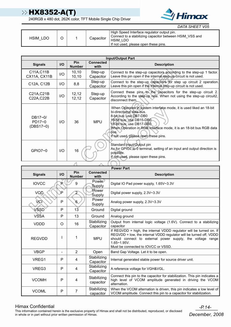
HSIM_LDO O 1 CapacitorHigh Speed Interface regulator output pin. Connect to a stabilizing capacitor between HSIM_VSS and HSIM_LDO If not used, please open these pins.
Input/Output Part
Signals I/O Pin Number
Connected with Description
C11A,C11B CX11A, CX11B I/O 10,10
10,10 Step-up
CapacitorConnect to the step-up capacitors according to the step-up 1 factor. Leave this pin open if the internal step-up circuit is not used.
C12A, C12B I/O 8,8 Step-up Capacitor
Connect to the step-up capacitors for step up circuit 2 operation. Leave this pin open if the internal step-up circuit is not used.
C21A,C21B C22A,C22B I/O 12,12
12,12 Step-up
CapacitorConnect these pins to the capacitors for the step-up circuit 2. According to the step-up rate. When not using the step-up circuit2, disconnect them.
DB17~0/ PD17~0
(DBS17~0) I/O 36 MPU
When Operates in system interface mode, it is used liked an 18-bit bi-directional data bus. 8-bit bus: use DB7-DB0 16-bit bus: use DB15-DB0 18-bit bus: use DB17-DB0 When Operation in RGB interface mode, it is an 18-bit bus RGB data bus. If not used, please open these pins.
GPIO7~0 I/O 16 - Standard Input/Output pin As for GPIO7 to 0 terminal, setting of an input and output direction is possible. If not used, please open these pins.
Power Part
Signals I/O Pin Number
Connected with Description
IOVCC P 9 Power Supply Digital IO Pad power supply, 1.65V~3.3V
VCC P 2 Power Supply Digital power supply, 2.3V~3.3V
VCI P 6 Power Supply Analog power supply, 2.3V~3.3V
VSSD P 13 Ground Digital ground
VSSA P 13 Ground Analog ground
VDDD O 16 Stabilizing Capacitor
Output from internal logic voltage (1.6V). Connect to a stabilizing capacitor
REGVDD I 1 MPU
If REGVDD = high, the internal VDDD regulator will be turned on. If REGVDD = low, the internal VDDD regulator will be turned off, VDDD should connect to external power supply, the voltage range 1.65~1.95V. Must be connected to IOVCC or VSSD.
VBGP - 2 Open Band Gap Voltage. Let it to be open.
VREG1 P 4 Stabilizing Capacitor Internal generated stable power for source driver unit.
VREG3 P 4 Stabilizing Capacitor A reference voltage for VGH&VGL.
VCOMH P 4 Stabilizing capacitor
Connect this pin to the capacitor for stabilization. This pin indicates a high level of VCOM amplitude generated in driving the VCOM alternation.
VCOML P 7 Stabilizing capacitor
When the VCOM alternation is driven, this pin indicates a low level of VCOM amplitude. Connect this pin to a capacitor for stabilization.
-P.15- Himax Confidential
December, 2008This information contained herein is the exclusive property of Himax and shall not be distributed, reproduced, or disclosed in whole or in part without prior written permission of Himax.
HX8352-A(T) 240RGB x 480 dot, 262K color, TFT Mobile Single Chip Driver
DATA SHEET V05Power Part
Signals I/O Pin Number
Connected with Description
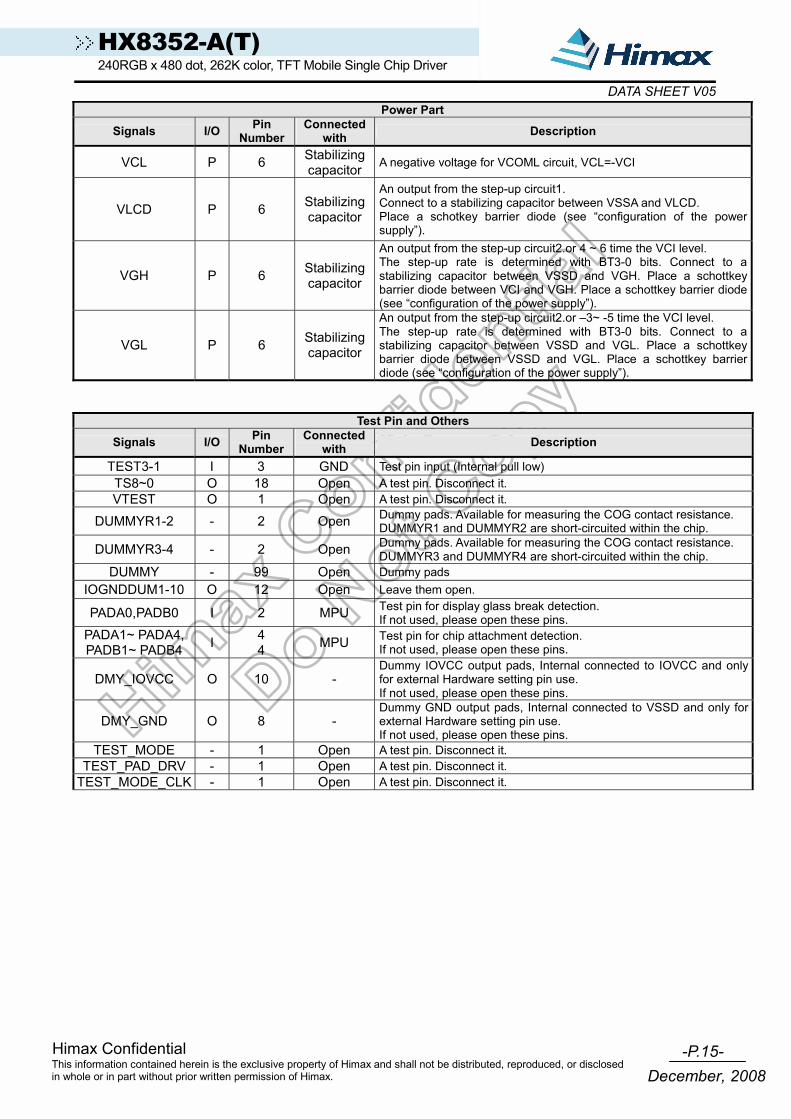
VCL P 6 Stabilizing capacitor A negative voltage for VCOML circuit, VCL=-VCI
VLCD P 6 Stabilizing capacitor
An output from the step-up circuit1. Connect to a stabilizing capacitor between VSSA and VLCD. Place a schotkey barrier diode (see “configuration of the power supply”).
VGH P 6 Stabilizing capacitor
An output from the step-up circuit2.or 4 ~ 6 time the VCI level. The step-up rate is determined with BT3-0 bits. Connect to a stabilizing capacitor between VSSD and VGH. Place a schottkey barrier diode between VCI and VGH. Place a schottkey barrier diode (see “configuration of the power supply”).
VGL P 6 Stabilizing capacitor
An output from the step-up circuit2.or –3~ -5 time the VCI level. The step-up rate is determined with BT3-0 bits. Connect to a stabilizing capacitor between VSSD and VGL. Place a schottkey barrier diode between VSSD and VGL. Place a schottkey barrier diode (see “configuration of the power supply”).
Test Pin and Others
Signals I/O Pin Number
Connectedwith Description
TEST3-1 I 3 GND Test pin input (Internal pull low) TS8~0 O 18 Open A test pin. Disconnect it. VTEST O 1 Open A test pin. Disconnect it.
DUMMYR1-2 - 2 Open Dummy pads. Available for measuring the COG contact resistance. DUMMYR1 and DUMMYR2 are short-circuited within the chip.
DUMMYR3-4 - 2 Open Dummy pads. Available for measuring the COG contact resistance. DUMMYR3 and DUMMYR4 are short-circuited within the chip.
DUMMY - 99 Open Dummy pads IOGNDDUM1-10 O 12 Open Leave them open.
PADA0,PADB0 I 2 MPU Test pin for display glass break detection. If not used, please open these pins.
PADA1~ PADA4, PADB1~ PADB4 I 4
4 MPU Test pin for chip attachment detection. If not used, please open these pins.
DMY_IOVCC O 10 - Dummy IOVCC output pads, Internal connected to IOVCC and only for external Hardware setting pin use. If not used, please open these pins.
DMY_GND O 8 - Dummy GND output pads, Internal connected to VSSD and only for external Hardware setting pin use. If not used, please open these pins.
TEST_MODE - 1 Open A test pin. Disconnect it. TEST_PAD_DRV - 1 Open A test pin. Disconnect it.
TEST_MODE_CLK - 1 Open A test pin. Disconnect it.

-P.16- Himax Confidential
December, 2008This information contained herein is the exclusive property of Himax and shall not be distributed, reproduced, or disclosed in whole or in part without prior written permission of Himax.
HX8352-A(T) 240RGB x 480 dot, 262K color, TFT Mobile Single Chip Driver
DATA SHEET V054.2 Pin assignment
DUMMY
HX 8352-A
Pin Assignment
( Bump View)FACE UP
NO.1681
DUMMY
PADA1PADB1PADA0
DUMMYR1DUMMYR2
NO.23
NO.38
NO.51
NO.60
NO.82
VDDD
VDDD
VSSA
VBGPVBGP
DMY_GNDEXTC
DMY_IOVCCIOVCC
IOVCCVSSD
VSSDVSSA
DMY_IOVCC
BS2
BS1DMY_GND
BS0DMY_IOVCC
TEST1
DB15DB15DB16DB16DB17DB17
DOTCLK
DMY_GNDVSYNC
DMY_IOVCC
DB11
DUMMYDB14DB14
DB13DB13
DB12DB12
DB8DB8DB9DB9
DB10DB10
DUMMYDUMMY
DB6DB6DB7DB7
TEST3
DUMMYDUMMY
DB3DB3DB4DB4DB5DB5
SDODB0DB0DB1DB1
DB2DB2
DUMMY
TS8TS8
DUMMYDUMMY
TETE
BURNNISDNISD
DUMMYNCS
NWR_RNW
SDISDO
TS3TS3TS4TS4
TS5TS5TS6TS6TS7TS7
NCS2NCS2
RS2RS2
RES_SEL1
RES_SEL0
REGVDD
DUMMY
TS0TS0TS1TS1TS2TS2
PWM_OUTPWM_OUT
NWR2NWR2
E2E2
DUMMY
STB+
IOGNDDUM3
GPIO7
GPIO1
VREG3VREG3
DUMMY
VGL
C11AC11B
C11BCX11A
CX11ACX11B
CX11BVLCD
VREG3
DUMMYC11A
C12AC12B
C12BDUMMY
VCI
VCIVCCVCC
C22A
C22BC21A
C21AC21B
C21BC12A
DUMMY
DB11
VREG3
VLCD
DUMMY
PADA2PADB2PADB0
DUMMYR4DUMMYR3
DUMMY
DUMMY
DUMMY
G432
PADB3
PADA3
G6
G2
G4
DUMMY
DUMMY
DUMMY
DUMMY
S720S719
S718
S361
S362
S363
DUMMY
DUMMY
GPIO2
GPIO3
GPIO4
GPIO5
GPIO6
C22B
NO.320
NO.326
NO.335
NO.355
NO.369
NO.376
NO.384
NO.392
NO.404
NO.416
NO.447
S360
S359
S2S1
DUMMYDUMMYDUMMYDUMMY
S3
G1G3
G5
DUMMY
DUMMY
G431
G429
NO.478
NO.695
NO.704
NO.1059
NO.1091
NO.1449
NO.1458
NO.1670
NO.1675
GPIO1
GPIO2
GPIO3
GPIO4
GPIO5
GPIO6
GPIO7
DMY_IOVCC
VGH
VGH
VGL
C22A
DU
MM
Y
DU
MM
Y
DU
MM
Y
G4
80
G4
78
DU
MM
Y
DU
MM
Y
DU
MM
Y
DU
MM
Y
G4
34
G4
36
NO.472
DU
MM
Y
DU
MM
Y
DU
MM
Y
DU
MM
Y
G43
3
G43
5
G47
7G
479
DU
MM
Y
DU
MM
Y
DU
MM
Y
NO.1702
NO.1
GPIO0GPIO0
VCL
VCL
DUMMY
DUMMY
NO.428
DUMMY
DUMMY
TEST_MODETEST_PAD_DRV
TEST_MODE_CLK
DUMMYDUMMY
OSC
DUMMYIOGNDDUM1
HSIM_VCC
HSIM_VCC
HSIM_LDOIOGNDDUM2
HSIM_VSS
HSIM_VSS
STB+
IOGNDDUM4
STB-STB-
IOGNDDUM5
DATA+DATA+
IOGNDDUM6
DATA-DATA-
IOGNDDUM7IOGNDDUM8
VGSVGS
VTEST
VCOM
VCOM
VCOMHVCOMH
VCOMHVCOMH
VCOML
VCOML
VREG1VREG1VREG1VREG1
VCOMRVCOMR
NO.345
DMY_GNDP68
TEST2NRESET
NRESETDUMMY
DUMMYDUMMY
NRD_E
IFSEL0
DNC_SCL
DUMMYDUMMY
IOGNDDUM9IOGNDDUM9
IOGNDDUM10IOGNDDUM10
G430
PADA4
PADB4
NO.233
NO.241
NO.265
NO.296
NO.302
NO.308
DMY_IOVCCHSYNC
DMY_GNDENABLE
DMY_IOVCC
DMY_IOVCC
DMY_GND
DMY_IOVCC
DMY_GND
DMY_GND
DMY_IOVCC
NO.272
Chip Size: 18680 um x 1020 um (Including Seal-ring 20 um *2 Scribe line 40 um *2)
Chip Thickness: 300 um (typ.)
Pad Location: Pad center
Coordinate Origin: Chip center
Au Bump Size:1. 24 um x 120 um Input/Output (No. 1~ No. 446)
2. 106 um x 14 um Staggered LCD output side (No. 447 ~ No. 477)
3. 14 um x 106 um Staggered LCD output side (No. 478 ~ No. 1675)
4. 106 um x 14 um Staggered LCD output side (No. 1676 ~ No. 1706)

-P.17- Himax Confidential
December, 2008This information contained herein is the exclusive property of Himax and shall not be distributed, reproduced, or disclosed in whole or in part without prior written permission of Himax.
HX8352-A(T) 240RGB x 480 dot, 262K color, TFT Mobile Single Chip Driver
DATA SHEET V054.3 PAD coordinates
No. Name X Y No. Name X Y No. Name X Y No. Name X Y 1 DUMMY -9189 -385 61 DMY_IOVCC -6789 -385 121 DB7 -4389 -385 181 DMY_IOVCC -1989 -3852 DUMMY -9149 -385 62 EXTC -6749 -385 122 DB6 -4349 -385 182 RS2 -1949 -3853 PADA1 -9109 -385 63 DMY_GND -6709 -385 123 DB6 -4309 -385 183 RS2 -1909 -3854 PADB1 -9069 -385 64 TEST1 -6669 -385 124 DB5 -4269 -385 184 NCS2 -1869 -3855 PADA0 -9029 -385 65 DMY_IOVCC -6629 -385 125 DB5 -4229 -385 185 NCS2 -1829 -3856 DUMMYR1 -8989 -385 66 BS0 -6589 -385 126 DB4 -4189 -385 186 E2 -1789 -3857 DUMMYR2 -8949 -385 67 DMY_GND -6549 -385 127 DB4 -4149 -385 187 E2 -1749 -3858 VDDD -8909 -385 68 BS1 -6509 -385 128 DB3 -4109 -385 188 NWR2 -1709 -3859 VDDD -8869 -385 69 DMY_IOVCC -6469 -385 129 DB3 -4069 -385 189 NWR2 -1669 -385
10 VDDD -8829 -385 70 BS2 -6429 -385 130 DB2 -4029 -385 190 PWM_OUT -1629 -38511 VDDD -8789 -385 71 DMY_GND -6389 -385 131 DB2 -3989 -385 191 PWM_OUT -1589 -38512 VDDD -8749 -385 72 P68 -6349 -385 132 DUMMY -3949 -385 192 GPIO0 -1549 -38513 VDDD -8709 -385 73 DMY_IOVCC -6309 -385 133 DUMMY -3909 -385 193 GPIO0 -1509 -38514 VDDD -8669 -385 74 TEST2 -6269 -385 134 DB1 -3869 -385 194 DUMMY -1469 -38515 VDDD -8629 -385 75 NRESET -6229 -385 135 DB1 -3829 -385 195 DUMMY -1429 -38516 VDDD -8589 -385 76 NRESET -6189 -385 136 DB0 -3789 -385 196 GPIO1 -1389 -38517 VDDD -8549 -385 77 NRESET -6149 -385 137 DB0 -3749 -385 197 GPIO1 -1349 -38518 VDDD -8509 -385 78 NRESET -6109 -385 138 SDO -3709 -385 198 GPIO2 -1309 -38519 VDDD -8469 -385 79 NRESET -6069 -385 139 SDO -3669 -385 199 GPIO2 -1269 -38520 VDDD -8429 -385 80 NRESET -6029 -385 140 SDI -3629 -385 200 GPIO3 -1229 -38521 VDDD -8389 -385 81 NRESET -5989 -385 141 NRD_E -3589 -385 201 GPIO3 -1189 -38522 VDDD -8349 -385 82 NRESET -5949 -385 142 NWR_RNW -3549 -385 202 GPIO4 -1149 -38523 VDDD -8309 -385 83 DUMMY -5909 -385 143 DMY_IOVCC -3509 -385 203 GPIO4 -1109 -38524 VBGP -8269 -385 84 DMY_IOVCC -5869 -385 144 IFSEL0 -3469 -385 204 GPIO5 -1069 -38525 VBGP -8229 -385 85 VSYNC -5829 -385 145 DMY_GND -3429 -385 205 GPIO5 -1029 -38526 VSSA -8189 -385 86 DMY_GND -5789 -385 146 DNC_SCL -3389 -385 206 GPIO6 -989 -38527 VSSA -8149 -385 87 HSYNC -5749 -385 147 NCS -3349 -385 207 GPIO6 -949 -38528 VSSA -8109 -385 88 DMY_IOVCC -5709 -385 148 DUMMY -3309 -385 208 DUMMY -909 -38529 VSSA -8069 -385 89 DOTCLK -5669 -385 149 DUMMY -3269 -385 209 DUMMY -869 -38530 VSSA -8029 -385 90 DMY_GND -5629 -385 150 NISD -3229 -385 210 DUMMY -829 -38531 VSSA -7989 -385 91 ENABLE -5589 -385 151 NISD -3189 -385 211 DUMMY -789 -38532 VSSA -7949 -385 92 DMY_IOVCC -5549 -385 152 BURN -3149 -385 212 GPIO7 -749 -38533 VSSA -7909 -385 93 DB17 -5509 -385 153 TE -3109 -385 213 GPIO7 -709 -38534 VSSA -7869 -385 94 DB17 -5469 -385 154 TE -3069 -385 214 TEST_MODE -669 -38535 VSSA -7829 -385 95 DB16 -5429 -385 155 TS8 -3029 -385 215 TEST_PAD_DRV -629 -38536 VSSA -7789 -385 96 DB16 -5389 -385 156 TS8 -2989 -385 216 IOGNDDUM9 -589 -38537 VSSA -7749 -385 97 DB15 -5349 -385 157 TS7 -2949 -385 217 IOGNDDUM9 -549 -38538 VSSA -7709 -385 98 DB15 -5309 -385 158 TS7 -2909 -385 218 TEST_MODE_CLK -509 -38539 VSSD -7669 -385 99 DB14 -5269 -385 159 TS6 -2869 -385 219 IOGNDDUM10 -469 -38540 VSSD -7629 -385 100 DB14 -5229 -385 160 TS6 -2829 -385 220 IOGNDDUM10 -429 -38541 VSSD -7589 -385 101 DUMMY -5189 -385 161 TS5 -2789 -385 221 OSC -389 -38542 VSSD -7549 -385 102 DUMMY -5149 -385 162 TS5 -2749 -385 222 DUMMY -349 -38543 VSSD -7509 -385 103 DB13 -5109 -385 163 DUMMY -2709 -385 223 DUMMY -309 -38544 VSSD -7469 -385 104 DB13 -5069 -385 164 DUMMY -2669 -385 224 DUMMY 309 -38545 VSSD -7429 -385 105 DB12 -5029 -385 165 TS4 -2629 -385 225 IOGNDDUM1 349 -38546 VSSD -7389 -385 106 DB12 -4989 -385 166 TS4 -2589 -385 226 HSIM_VCC 389 -38547 VSSD -7349 -385 107 DB11 -4949 -385 167 TS3 -2549 -385 227 HSIM_VCC 429 -38548 VSSD -7309 -385 108 DB11 -4909 -385 168 TS3 -2509 -385 228 HSIM_VCC 469 -38549 VSSD -7269 -385 109 DB10 -4869 -385 169 TS2 -2469 -385 229 HSIM_VCC 509 -38550 VSSD -7229 -385 110 DB10 -4829 -385 170 TS2 -2429 -385 230 HSIM_VCC 549 -38551 VSSD -7189 -385 111 DB9 -4789 -385 171 TS1 -2389 -385 231 HSIM_VCC 589 -38552 IOVCC -7149 -385 112 DB9 -4749 -385 172 TS1 -2349 -385 232 HSIM_VCC 629 -38553 IOVCC -7109 -385 113 DB8 -4709 -385 173 TS0 -2309 -385 233 HSIM_VCC 669 -38554 IOVCC -7069 -385 114 DB8 -4669 -385 174 TS0 -2269 -385 234 IOGNDDUM2 709 -38555 IOVCC -7029 -385 115 DUMMY -4629 -385 175 DMY_GND -2229 -385 235 HSIM_LDO 749 -38556 IOVCC -6989 -385 116 DUMMY -4589 -385 176 REGVDD -2189 -385 236 HSIM_VSS 789 -38557 IOVCC -6949 -385 117 DUMMY -4549 -385 177 DMY_IOVCC -2149 -385 237 HSIM_VSS 829 -38558 IOVCC -6909 -385 118 DUMMY -4509 -385 178 RES_SEL0 -2109 -385 238 HSIM_VSS 869 -38559 IOVCC -6869 -385 119 TEST3 -4469 -385 179 DMY_GND -2069 -385 239 HSIM_VSS 909 -38560 IOVCC -6829 -385 120 DB7 -4429 -385 180 RES_SEL1 -2029 -385 240 HSIM_VSS 949 -385

-P.18- Himax Confidential
December, 2008This information contained herein is the exclusive property of Himax and shall not be distributed, reproduced, or disclosed in whole or in part without prior written permission of Himax.
HX8352-A(T) 240RGB x 480 dot, 262K color, TFT Mobile Single Chip Driver
DATA SHEET V05
No. Name X Y No. Name X Y No. Name X Y No. Name X Y 241 HSIM_VSS 989 -385 301 VCL 3389 -385 361 C11A 5789 -385 421 C22B 8189 -385242 IOGNDDUM3 1029 -385 302 VCL 3429 -385 362 C11A 5829 -385 422 C22B 8229 -385243 STB- 1069 -385 303 VGH 3469 -385 363 C11A 5869 -385 423 C22B 8269 -385244 STB- 1109 -385 304 VGH 3509 -385 364 C11A 5909 -385 424 C22B 8309 -385245 IOGNDDUM4 1149 -385 305 VGH 3549 -385 365 C11A 5949 -385 425 C22B 8349 -385246 STB+ 1189 -385 306 VGH 3589 -385 366 DUMMY 5989 -385 426 C22B 8389 -385247 STB+ 1229 -385 307 VGH 3629 -385 367 VCC 6029 -385 427 C22B 8429 -385248 IOGNDDUM5 1269 -385 308 VGH 3669 -385 368 VCC 6069 -385 428 C22A 8469 -385249 DATA- 1309 -385 309 VGL 3709 -385 369 VCI 6109 -385 429 C22A 8509 -385250 DATA- 1349 -385 310 VGL 3749 -385 370 VCI 6149 -385 430 C22A 8549 -385251 IOGNDDUM6 1389 -385 311 VGL 3789 -385 371 VCI 6189 -385 431 C22A 8589 -385252 DATA+ 1429 -385 312 VGL 3829 -385 372 VCI 6229 -385 432 C22A 8629 -385253 DATA+ 1469 -385 313 VGL 3869 -385 373 VCI 6269 -385 433 C22A 8669 -385254 IOGNDDUM7 1509 -385 314 VGL 3909 -385 374 VCI 6309 -385 434 C22A 8709 -385255 IOGNDDUM8 1549 -385 315 DUMMY 3949 -385 375 DUMMY 6349 -385 435 C22A 8749 -385256 VGS 1589 -385 316 VREG3 3989 -385 376 C12B 6389 -385 436 C22A 8789 -385257 VGS 1629 -385 317 VREG3 4029 -385 377 C12B 6429 -385 437 C22A 8829 -385258 VTEST 1669 -385 318 VREG3 4069 -385 378 C12B 6469 -385 438 C22A 8869 -385259 VCOM 1709 -385 319 VREG3 4109 -385 379 C12B 6509 -385 439 C22A 8909 -385260 VCOM 1749 -385 320 VLCD 4149 -385 380 C12B 6549 -385 440 DUMMYR3 8949 -385261 VCOM 1789 -385 321 VLCD 4189 -385 381 C12B 6589 -385 441 DUMMYR4 8989 -385262 VCOM 1829 -385 322 VLCD 4229 -385 382 C12B 6629 -385 442 PADB0 9029 -385263 VCOM 1869 -385 323 VLCD 4269 -385 383 C12B 6669 -385 443 PADB2 9069 -385264 VCOM 1909 -385 324 VLCD 4309 -385 384 C12A 6709 -385 444 PADA2 9109 -385265 VCOM 1949 -385 325 VLCD 4349 -385 385 C12A 6749 -385 445 DUMMY 9149 -385266 VCOML 1989 -385 326 CX11B 4389 -385 386 C12A 6789 -385 446 DUMMY 9189 -385267 VCOML 2029 -385 327 CX11B 4429 -385 387 C12A 6829 -385 447 DUMMY 9223 -238268 VCOML 2069 -385 328 CX11B 4469 -385 388 C12A 6869 -385 448 DUMMY 9101 -222269 VCOML 2109 -385 329 CX11B 4509 -385 389 C12A 6909 -385 449 DUMMY 9223 -206270 VCOML 2149 -385 330 CX11B 4549 -385 390 C12A 6949 -385 450 G480 9101 -190271 VCOML 2189 -385 331 CX11B 4589 -385 391 C12A 6989 -385 451 G478 9223 -174272 VCOML 2229 -385 332 CX11B 4629 -385 392 C21B 7029 -385 452 G476 9101 -158273 VCOMH 2269 -385 333 CX11B 4669 -385 393 C21B 7069 -385 453 G474 9223 -142274 VCOMH 2309 -385 334 CX11B 4709 -385 394 C21B 7109 -385 454 G472 9101 -126275 VCOMH 2349 -385 335 CX11B 4749 -385 395 C21B 7149 -385 455 G470 9223 -110276 VCOMH 2389 -385 336 CX11A 4789 -385 396 C21B 7189 -385 456 G468 9101 -94277 VREG1 2429 -385 337 CX11A 4829 -385 397 C21B 7229 -385 457 G466 9223 -78278 VREG1 2469 -385 338 CX11A 4869 -385 398 C21B 7269 -385 458 G464 9101 -62279 VREG1 2509 -385 339 CX11A 4909 -385 399 C21B 7309 -385 459 G462 9223 -46280 VREG1 2549 -385 340 CX11A 4949 -385 400 C21B 7349 -385 460 G460 9101 -30281 VCOMR 2589 -385 341 CX11A 4989 -385 401 C21B 7389 -385 461 G458 9223 -14282 VCOMR 2629 -385 342 CX11A 5029 -385 402 C21B 7429 -385 462 G456 9101 2 283 DUMMY 2669 -385 343 CX11A 5069 -385 403 C21B 7469 -385 463 G454 9223 18284 DUMMY 2709 -385 344 CX11A 5109 -385 404 C21A 7509 -385 464 G452 9101 34285 DUMMY 2749 -385 345 CX11A 5149 -385 405 C21A 7549 -385 465 G450 9223 50286 DUMMY 2789 -385 346 C11B 5189 -385 406 C21A 7589 -385 466 G448 9101 66287 DUMMY 2829 -385 347 C11B 5229 -385 407 C21A 7629 -385 467 G446 9223 82288 DUMMY 2869 -385 348 C11B 5269 -385 408 C21A 7669 -385 468 G444 9101 98289 DUMMY 2909 -385 349 C11B 5309 -385 409 C21A 7709 -385 469 G442 9223 114290 DUMMY 2949 -385 350 C11B 5349 -385 410 C21A 7749 -385 470 G440 9101 130291 DUMMY 2989 -385 351 C11B 5389 -385 411 C21A 7789 -385 471 G438 9223 146292 DUMMY 3029 -385 352 C11B 5429 -385 412 C21A 7829 -385 472 G436 9101 162293 DUMMY 3069 -385 353 C11B 5469 -385 413 C21A 7869 -385 473 G434 9223 178294 DUMMY 3109 -385 354 C11B 5509 -385 414 C21A 7909 -385 474 DUMMY 9101 194295 DUMMY 3149 -385 355 C11B 5549 -385 415 C21A 7949 -385 475 DUMMY 9223 210296 DUMMY 3189 -385 356 C11A 5589 -385 416 C22B 7989 -385 476 DUMMY 9101 226297 VCL 3229 -385 357 C11A 5629 -385 417 C22B 8029 -385 477 DUMMY 9223 242298 VCL 3269 -385 358 C11A 5669 -385 418 C22B 8069 -385 478 DUMMY 9007 393299 VCL 3309 -385 359 C11A 5709 -385 419 C22B 8109 -385 479 DUMMY 8991 271300 VCL 3349 -385 360 C11A 5749 -385 420 C22B 8149 -385 480 PADA3 8975 393

-P.19- Himax Confidential
December, 2008This information contained herein is the exclusive property of Himax and shall not be distributed, reproduced, or disclosed in whole or in part without prior written permission of Himax.
HX8352-A(T) 240RGB x 480 dot, 262K color, TFT Mobile Single Chip Driver
DATA SHEET V05
No. Name X Y No. Name X Y No. Name X Y No. Name X Y 481 PADB3 8959 271 541 G314 7999 271 601 G194 7039 271 661 G74 6079 271 482 G432 8943 393 542 G312 7983 393 602 G192 7023 393 662 G72 6063 393 483 G430 8927 271 543 G310 7967 271 603 G190 7007 271 663 G70 6047 271 484 G428 8911 393 544 G308 7951 393 604 G188 6991 393 664 G68 6031 393 485 G426 8895 271 545 G306 7935 271 605 G186 6975 271 665 G66 6015 271 486 G424 8879 393 546 G304 7919 393 606 G184 6959 393 666 G64 5999 393 487 G422 8863 271 547 G302 7903 271 607 G182 6943 271 667 G62 5983 271 488 G420 8847 393 548 G300 7887 393 608 G180 6927 393 668 G60 5967 393 489 G418 8831 271 549 G298 7871 271 609 G178 6911 271 669 G58 5951 271 490 G416 8815 393 550 G296 7855 393 610 G176 6895 393 670 G56 5935 393 491 G414 8799 271 551 G294 7839 271 611 G174 6879 271 671 G54 5919 271 492 G412 8783 393 552 G292 7823 393 612 G172 6863 393 672 G52 5903 393 493 G410 8767 271 553 G290 7807 271 613 G170 6847 271 673 G50 5887 271 494 G408 8751 393 554 G288 7791 393 614 G168 6831 393 674 G48 5871 393 495 G406 8735 271 555 G286 7775 271 615 G166 6815 271 675 G46 5855 271 496 G404 8719 393 556 G284 7759 393 616 G164 6799 393 676 G44 5839 393 497 G402 8703 271 557 G282 7743 271 617 G162 6783 271 677 G42 5823 271 498 G400 8687 393 558 G280 7727 393 618 G160 6767 393 678 G40 5807 393 499 G398 8671 271 559 G278 7711 271 619 G158 6751 271 679 G38 5791 271 500 G396 8655 393 560 G276 7695 393 620 G156 6735 393 680 G36 5775 393 501 G394 8639 271 561 G274 7679 271 621 G154 6719 271 681 G34 5759 271 502 G392 8623 393 562 G272 7663 393 622 G152 6703 393 682 G32 5743 393 503 G390 8607 271 563 G270 7647 271 623 G150 6687 271 683 G30 5727 271 504 G388 8591 393 564 G268 7631 393 624 G148 6671 393 684 G28 5711 393 505 G386 8575 271 565 G266 7615 271 625 G146 6655 271 685 G26 5695 271 506 G384 8559 393 566 G264 7599 393 626 G144 6639 393 686 G24 5679 393 507 G382 8543 271 567 G262 7583 271 627 G142 6623 271 687 G22 5663 271 508 G380 8527 393 568 G260 7567 393 628 G140 6607 393 688 G20 5647 393 509 G378 8511 271 569 G258 7551 271 629 G138 6591 271 689 G18 5631 271 510 G376 8495 393 570 G256 7535 393 630 G136 6575 393 690 G16 5615 393 511 G374 8479 271 571 G254 7519 271 631 G134 6559 271 691 G14 5599 271 512 G372 8463 393 572 G252 7503 393 632 G132 6543 393 692 G12 5583 393 513 G370 8447 271 573 G250 7487 271 633 G130 6527 271 693 G10 5567 271 514 G368 8431 393 574 G248 7471 393 634 G128 6511 393 694 G8 5551 393 515 G366 8415 271 575 G246 7455 271 635 G126 6495 271 695 G6 5535 271 516 G364 8399 393 576 G244 7439 393 636 G124 6479 393 696 G4 5519 393 517 G362 8383 271 577 G242 7423 271 637 G122 6463 271 697 G2 5503 271 518 G360 8367 393 578 G240 7407 393 638 G120 6447 393 698 DUMMY 5487 393 519 G358 8351 271 579 G238 7391 271 639 G118 6431 271 699 DUMMY 5471 271 520 G356 8335 393 580 G236 7375 393 640 G116 6415 393 700 DUMMY 5455 393 521 G354 8319 271 581 G234 7359 271 641 G114 6399 271 701 DUMMY 5441 271 522 G352 8303 393 582 G232 7343 393 642 G112 6383 393 702 S720 5427 393 523 G350 8287 271 583 G230 7327 271 643 G110 6367 271 703 S719 5413 271 524 G348 8271 393 584 G228 7311 393 644 G108 6351 393 704 S718 5399 393 525 G346 8255 271 585 G226 7295 271 645 G106 6335 271 705 S717 5385 271 526 G344 8239 393 586 G224 7279 393 646 G104 6319 393 706 S716 5371 393 527 G342 8223 271 587 G222 7263 271 647 G102 6303 271 707 S715 5357 271 528 G340 8207 393 588 G220 7247 393 648 G100 6287 393 708 S714 5343 393 529 G338 8191 271 589 G218 7231 271 649 G98 6271 271 709 S713 5329 271 530 G336 8175 393 590 G216 7215 393 650 G96 6255 393 710 S712 5315 393 531 G334 8159 271 591 G214 7199 271 651 G94 6239 271 711 S711 5301 271 532 G332 8143 393 592 G212 7183 393 652 G92 6223 393 712 S710 5287 393 533 G330 8127 271 593 G210 7167 271 653 G90 6207 271 713 S709 5273 271 534 G328 8111 393 594 G208 7151 393 654 G88 6191 393 714 S708 5259 393 535 G326 8095 271 595 G206 7135 271 655 G86 6175 271 715 S707 5245 271 536 G324 8079 393 596 G204 7119 393 656 G84 6159 393 716 S706 5231 393 537 G322 8063 271 597 G202 7103 271 657 G82 6143 271 717 S705 5217 271 538 G320 8047 393 598 G200 7087 393 658 G80 6127 393 718 S704 5203 393 539 G318 8031 271 599 G198 7071 271 659 G78 6111 271 719 S703 5189 271 540 G316 8015 393 600 G196 7055 393 660 G76 6095 393 720 S702 5175 393
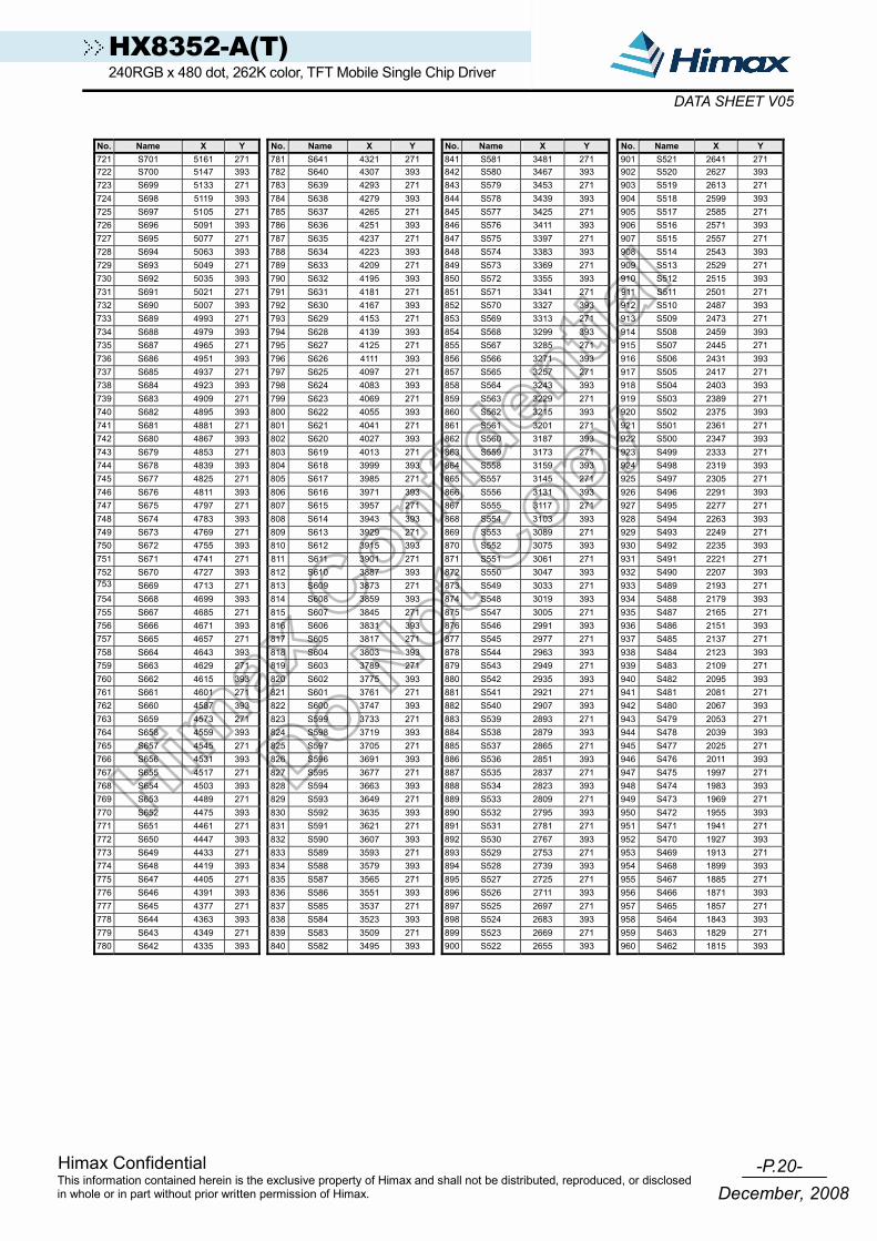
-P.20- Himax Confidential
December, 2008This information contained herein is the exclusive property of Himax and shall not be distributed, reproduced, or disclosed in whole or in part without prior written permission of Himax.
HX8352-A(T) 240RGB x 480 dot, 262K color, TFT Mobile Single Chip Driver
DATA SHEET V05
No. Name X Y No. Name X Y No. Name X Y No. Name X Y 721 S701 5161 271 781 S641 4321 271 841 S581 3481 271 901 S521 2641 271 722 S700 5147 393 782 S640 4307 393 842 S580 3467 393 902 S520 2627 393 723 S699 5133 271 783 S639 4293 271 843 S579 3453 271 903 S519 2613 271 724 S698 5119 393 784 S638 4279 393 844 S578 3439 393 904 S518 2599 393 725 S697 5105 271 785 S637 4265 271 845 S577 3425 271 905 S517 2585 271 726 S696 5091 393 786 S636 4251 393 846 S576 3411 393 906 S516 2571 393 727 S695 5077 271 787 S635 4237 271 847 S575 3397 271 907 S515 2557 271 728 S694 5063 393 788 S634 4223 393 848 S574 3383 393 908 S514 2543 393 729 S693 5049 271 789 S633 4209 271 849 S573 3369 271 909 S513 2529 271 730 S692 5035 393 790 S632 4195 393 850 S572 3355 393 910 S512 2515 393 731 S691 5021 271 791 S631 4181 271 851 S571 3341 271 911 S511 2501 271 732 S690 5007 393 792 S630 4167 393 852 S570 3327 393 912 S510 2487 393 733 S689 4993 271 793 S629 4153 271 853 S569 3313 271 913 S509 2473 271 734 S688 4979 393 794 S628 4139 393 854 S568 3299 393 914 S508 2459 393 735 S687 4965 271 795 S627 4125 271 855 S567 3285 271 915 S507 2445 271 736 S686 4951 393 796 S626 4111 393 856 S566 3271 393 916 S506 2431 393 737 S685 4937 271 797 S625 4097 271 857 S565 3257 271 917 S505 2417 271 738 S684 4923 393 798 S624 4083 393 858 S564 3243 393 918 S504 2403 393 739 S683 4909 271 799 S623 4069 271 859 S563 3229 271 919 S503 2389 271 740 S682 4895 393 800 S622 4055 393 860 S562 3215 393 920 S502 2375 393 741 S681 4881 271 801 S621 4041 271 861 S561 3201 271 921 S501 2361 271 742 S680 4867 393 802 S620 4027 393 862 S560 3187 393 922 S500 2347 393 743 S679 4853 271 803 S619 4013 271 863 S559 3173 271 923 S499 2333 271 744 S678 4839 393 804 S618 3999 393 864 S558 3159 393 924 S498 2319 393 745 S677 4825 271 805 S617 3985 271 865 S557 3145 271 925 S497 2305 271 746 S676 4811 393 806 S616 3971 393 866 S556 3131 393 926 S496 2291 393 747 S675 4797 271 807 S615 3957 271 867 S555 3117 271 927 S495 2277 271 748 S674 4783 393 808 S614 3943 393 868 S554 3103 393 928 S494 2263 393 749 S673 4769 271 809 S613 3929 271 869 S553 3089 271 929 S493 2249 271 750 S672 4755 393 810 S612 3915 393 870 S552 3075 393 930 S492 2235 393 751 S671 4741 271 811 S611 3901 271 871 S551 3061 271 931 S491 2221 271 752 S670 4727 393 812 S610 3887 393 872 S550 3047 393 932 S490 2207 393 753 S669 4713 271 813 S609 3873 271 873 S549 3033 271 933 S489 2193 271 754 S668 4699 393 814 S608 3859 393 874 S548 3019 393 934 S488 2179 393 755 S667 4685 271 815 S607 3845 271 875 S547 3005 271 935 S487 2165 271 756 S666 4671 393 816 S606 3831 393 876 S546 2991 393 936 S486 2151 393 757 S665 4657 271 817 S605 3817 271 877 S545 2977 271 937 S485 2137 271 758 S664 4643 393 818 S604 3803 393 878 S544 2963 393 938 S484 2123 393 759 S663 4629 271 819 S603 3789 271 879 S543 2949 271 939 S483 2109 271 760 S662 4615 393 820 S602 3775 393 880 S542 2935 393 940 S482 2095 393 761 S661 4601 271 821 S601 3761 271 881 S541 2921 271 941 S481 2081 271 762 S660 4587 393 822 S600 3747 393 882 S540 2907 393 942 S480 2067 393 763 S659 4573 271 823 S599 3733 271 883 S539 2893 271 943 S479 2053 271 764 S658 4559 393 824 S598 3719 393 884 S538 2879 393 944 S478 2039 393 765 S657 4545 271 825 S597 3705 271 885 S537 2865 271 945 S477 2025 271 766 S656 4531 393 826 S596 3691 393 886 S536 2851 393 946 S476 2011 393 767 S655 4517 271 827 S595 3677 271 887 S535 2837 271 947 S475 1997 271 768 S654 4503 393 828 S594 3663 393 888 S534 2823 393 948 S474 1983 393 769 S653 4489 271 829 S593 3649 271 889 S533 2809 271 949 S473 1969 271 770 S652 4475 393 830 S592 3635 393 890 S532 2795 393 950 S472 1955 393 771 S651 4461 271 831 S591 3621 271 891 S531 2781 271 951 S471 1941 271 772 S650 4447 393 832 S590 3607 393 892 S530 2767 393 952 S470 1927 393 773 S649 4433 271 833 S589 3593 271 893 S529 2753 271 953 S469 1913 271 774 S648 4419 393 834 S588 3579 393 894 S528 2739 393 954 S468 1899 393 775 S647 4405 271 835 S587 3565 271 895 S527 2725 271 955 S467 1885 271 776 S646 4391 393 836 S586 3551 393 896 S526 2711 393 956 S466 1871 393 777 S645 4377 271 837 S585 3537 271 897 S525 2697 271 957 S465 1857 271 778 S644 4363 393 838 S584 3523 393 898 S524 2683 393 958 S464 1843 393 779 S643 4349 271 839 S583 3509 271 899 S523 2669 271 959 S463 1829 271 780 S642 4335 393 840 S582 3495 393 900 S522 2655 393 960 S462 1815 393

-P.21- Himax Confidential
December, 2008This information contained herein is the exclusive property of Himax and shall not be distributed, reproduced, or disclosed in whole or in part without prior written permission of Himax.
HX8352-A(T) 240RGB x 480 dot, 262K color, TFT Mobile Single Chip Driver
DATA SHEET V05
No. Name X Y No. Name X Y No. Name X Y No. Name X Y 961 S461 1801 271 1021 S401 961 271 1081 DUMMY -135 393 1141 S311 -1087 393 962 S460 1787 393 1022 S400 947 393 1082 DUMMY -163 393 1142 S310 -1101 271 963 S459 1773 271 1023 S399 933 271 1083 DUMMY -191 393 1143 S309 -1115 393 964 S458 1759 393 1024 S398 919 393 1084 DUMMY -219 393 1144 S308 -1129 271 965 S457 1745 271 1025 S397 905 271 1085 DUMMY -247 393 1145 S307 -1143 393 966 S456 1731 393 1026 S396 891 393 1086 DUMMY -275 393 1146 S306 -1157 271 967 S455 1717 271 1027 S395 877 271 1087 DUMMY -303 393 1147 S305 -1171 393 968 S454 1703 393 1028 S394 863 393 1088 DUMMY -331 393 1148 S304 -1185 271 969 S453 1689 271 1029 S393 849 271 1089 DUMMY -359 393 1149 S303 -1199 393 970 S452 1675 393 1030 S392 835 393 1090 DUMMY -373 271 1150 S302 -1213 271 971 S451 1661 271 1031 S391 821 271 1091 DUMMY -387 393 1151 S301 -1227 393 972 S450 1647 393 1032 S390 807 393 1092 S360 -401 271 1152 S300 -1241 271 973 S449 1633 271 1033 S389 793 271 1093 S359 -415 393 1153 S299 -1255 393 974 S448 1619 393 1034 S388 779 393 1094 S358 -429 271 1154 S298 -1269 271 975 S447 1605 271 1035 S387 765 271 1095 S357 -443 393 1155 S297 -1283 393 976 S446 1591 393 1036 S386 751 393 1096 S356 -457 271 1156 S296 -1297 271 977 S445 1577 271 1037 S385 737 271 1097 S355 -471 393 1157 S295 -1311 393 978 S444 1563 393 1038 S384 723 393 1098 S354 -485 271 1158 S294 -1325 271 979 S443 1549 271 1039 S383 709 271 1099 S353 -499 393 1159 S293 -1339 393 980 S442 1535 393 1040 S382 695 393 1100 S352 -513 271 1160 S292 -1353 271 981 S441 1521 271 1041 S381 681 271 1101 S351 -527 393 1161 S291 -1367 393 982 S440 1507 393 1042 S380 667 393 1102 S350 -541 271 1162 S290 -1381 271 983 S439 1493 271 1043 S379 653 271 1103 S349 -555 393 1163 S289 -1395 393 984 S438 1479 393 1044 S378 639 393 1104 S348 -569 271 1164 S288 -1409 271 985 S437 1465 271 1045 S377 625 271 1105 S347 -583 393 1165 S287 -1423 393 986 S436 1451 393 1046 S376 611 393 1106 S346 -597 271 1166 S286 -1437 271 987 S435 1437 271 1047 S375 597 271 1107 S345 -611 393 1167 S285 -1451 393 988 S434 1423 393 1048 S374 583 393 1108 S344 -625 271 1168 S284 -1465 271 989 S433 1409 271 1049 S373 569 271 1109 S343 -639 393 1169 S283 -1479 393 990 S432 1395 393 1050 S372 555 393 1110 S342 -653 271 1170 S282 -1493 271 991 S431 1381 271 1051 S371 541 271 1111 S341 -667 393 1171 S281 -1507 393 992 S430 1367 393 1052 S370 527 393 1112 S340 -681 271 1172 S280 -1521 271 993 S429 1353 271 1053 S369 513 271 1113 S339 -695 393 1173 S279 -1535 393 994 S428 1339 393 1054 S368 499 393 1114 S338 -709 271 1174 S278 -1549 271 995 S427 1325 271 1055 S367 485 271 1115 S337 -723 393 1175 S277 -1563 393 996 S426 1311 393 1056 S366 471 393 1116 S336 -737 271 1176 S276 -1577 271 997 S425 1297 271 1057 S365 457 271 1117 S335 -751 393 1177 S275 -1591 393 998 S424 1283 393 1058 S364 443 393 1118 S334 -765 271 1178 S274 -1605 271 999 S423 1269 271 1059 S363 429 271 1119 S333 -779 393 1179 S273 -1619 393
1000 S422 1255 393 1060 S362 415 393 1120 S332 -793 271 1180 S272 -1633 271 1001 S421 1241 271 1061 S361 401 271 1121 S331 -807 393 1181 S271 -1647 393 1002 S420 1227 393 1062 DUMMY 387 393 1122 S330 -821 271 1182 S270 -1661 271 1003 S419 1213 271 1063 DUMMY 373 271 1123 S329 -835 393 1183 S269 -1675 393 1004 S418 1199 393 1064 DUMMY 359 393 1124 S328 -849 271 1184 S268 -1689 271 1005 S417 1185 271 1065 DUMMY 331 393 1125 S327 -863 393 1185 S267 -1703 393 1006 S416 1171 393 1066 DUMMY 303 393 1126 S326 -877 271 1186 S266 -1717 271 1007 S415 1157 271 1067 DUMMY 275 393 1127 S325 -891 393 1187 S265 -1731 393 1008 S414 1143 393 1068 DUMMY 247 393 1128 S324 -905 271 1188 S264 -1745 271 1009 S413 1129 271 1069 DUMMY 219 393 1129 S323 -919 393 1189 S263 -1759 393 1010 S412 1115 393 1070 DUMMY 191 393 1130 S322 -933 271 1190 S262 -1773 271 1011 S411 1101 271 1071 DUMMY 163 393 1131 S321 -947 393 1191 S261 -1787 393 1012 S410 1087 393 1072 DUMMY 135 393 1132 S320 -961 271 1192 S260 -1801 271 1013 S409 1073 271 1073 DUMMY 107 393 1133 S319 -975 393 1193 S259 -1815 393 1014 S408 1059 393 1074 DUMMY 79 393 1134 S318 -989 271 1194 S258 -1829 271 1015 S407 1045 271 1075 DUMMY 51 393 1135 S317 -1003 393 1195 S257 -1843 393 1016 S406 1031 393 1076 DUMMY 23 393 1136 S316 -1017 271 1196 S256 -1857 271 1017 S405 1017 271 1077 DUMMY -23 393 1137 S315 -1031 393 1197 S255 -1871 393 1018 S404 1003 393 1078 DUMMY -51 393 1138 S314 -1045 271 1198 S254 -1885 271 1019 S403 989 271 1079 DUMMY -79 393 1139 S313 -1059 393 1199 S253 -1899 393 1020 S402 975 393 1080 DUMMY -107 393 1140 S312 -1073 271 1200 S252 -1913 271

-P.22- Himax Confidential
December, 2008This information contained herein is the exclusive property of Himax and shall not be distributed, reproduced, or disclosed in whole or in part without prior written permission of Himax.
HX8352-A(T) 240RGB x 480 dot, 262K color, TFT Mobile Single Chip Driver
DATA SHEET V05
No. Name X Y No. Name X Y No. Name X Y No. Name X Y 1201 S251 -1927 393 1261 S191 -2767 393 1321 S131 -3607 393 1381 S71 -4447 393 1202 S250 -1941 271 1262 S190 -2781 271 1322 S130 -3621 271 1382 S70 -4461 271 1203 S249 -1955 393 1263 S189 -2795 393 1323 S129 -3635 393 1383 S69 -4475 393 1204 S248 -1969 271 1264 S188 -2809 271 1324 S128 -3649 271 1384 S68 -4489 271 1205 S247 -1983 393 1265 S187 -2823 393 1325 S127 -3663 393 1385 S67 -4503 393 1206 S246 -1997 271 1266 S186 -2837 271 1326 S126 -3677 271 1386 S66 -4517 271 1207 S245 -2011 393 1267 S185 -2851 393 1327 S125 -3691 393 1387 S65 -4531 393 1208 S244 -2025 271 1268 S184 -2865 271 1328 S124 -3705 271 1388 S64 -4545 271 1209 S243 -2039 393 1269 S183 -2879 393 1329 S123 -3719 393 1389 S63 -4559 393 1210 S242 -2053 271 1270 S182 -2893 271 1330 S122 -3733 271 1390 S62 -4573 271 1211 S241 -2067 393 1271 S181 -2907 393 1331 S121 -3747 393 1391 S61 -4587 393 1212 S240 -2081 271 1272 S180 -2921 271 1332 S120 -3761 271 1392 S60 -4601 271 1213 S239 -2095 393 1273 S179 -2935 393 1333 S119 -3775 393 1393 S59 -4615 393 1214 S238 -2109 271 1274 S178 -2949 271 1334 S118 -3789 271 1394 S58 -4629 271 1215 S237 -2123 393 1275 S177 -2963 393 1335 S117 -3803 393 1395 S57 -4643 393 1216 S236 -2137 271 1276 S176 -2977 271 1336 S116 -3817 271 1396 S56 -4657 271 1217 S235 -2151 393 1277 S175 -2991 393 1337 S115 -3831 393 1397 S55 -4671 393 1218 S234 -2165 271 1278 S174 -3005 271 1338 S114 -3845 271 1398 S54 -4685 271 1219 S233 -2179 393 1279 S173 -3019 393 1339 S113 -3859 393 1399 S53 -4699 393 1220 S232 -2193 271 1280 S172 -3033 271 1340 S112 -3873 271 1400 S52 -4713 271 1221 S231 -2207 393 1281 S171 -3047 393 1341 S111 -3887 393 1401 S51 -4727 393 1222 S230 -2221 271 1282 S170 -3061 271 1342 S110 -3901 271 1402 S50 -4741 271 1223 S229 -2235 393 1283 S169 -3075 393 1343 S109 -3915 393 1403 S49 -4755 393 1224 S228 -2249 271 1284 S168 -3089 271 1344 S108 -3929 271 1404 S48 -4769 271 1225 S227 -2263 393 1285 S167 -3103 393 1345 S107 -3943 393 1405 S47 -4783 393 1226 S226 -2277 271 1286 S166 -3117 271 1346 S106 -3957 271 1406 S46 -4797 271 1227 S225 -2291 393 1287 S165 -3131 393 1347 S105 -3971 393 1407 S45 -4811 393 1228 S224 -2305 271 1288 S164 -3145 271 1348 S104 -3985 271 1408 S44 -4825 271 1229 S223 -2319 393 1289 S163 -3159 393 1349 S103 -3999 393 1409 S43 -4839 393 1230 S222 -2333 271 1290 S162 -3173 271 1350 S102 -4013 271 1410 S42 -4853 271 1231 S221 -2347 393 1291 S161 -3187 393 1351 S101 -4027 393 1411 S41 -4867 393 1232 S220 -2361 271 1292 S160 -3201 271 1352 S100 -4041 271 1412 S40 -4881 271 1233 S219 -2375 393 1293 S159 -3215 393 1353 S99 -4055 393 1413 S39 -4895 393 1234 S218 -2389 271 1294 S158 -3229 271 1354 S98 -4069 271 1414 S38 -4909 271 1235 S217 -2403 393 1295 S157 -3243 393 1355 S97 -4083 393 1415 S37 -4923 393 1236 S216 -2417 271 1296 S156 -3257 271 1356 S96 -4097 271 1416 S36 -4937 271 1237 S215 -2431 393 1297 S155 -3271 393 1357 S95 -4111 393 1417 S35 -4951 393 1238 S214 -2445 271 1298 S154 -3285 271 1358 S94 -4125 271 1418 S34 -4965 271 1239 S213 -2459 393 1299 S153 -3299 393 1359 S93 -4139 393 1419 S33 -4979 393 1240 S212 -2473 271 1300 S152 -3313 271 1360 S92 -4153 271 1420 S32 -4993 271 1241 S211 -2487 393 1301 S151 -3327 393 1361 S91 -4167 393 1421 S31 -5007 393 1242 S210 -2501 271 1302 S150 -3341 271 1362 S90 -4181 271 1422 S30 -5021 271 1243 S209 -2515 393 1303 S149 -3355 393 1363 S89 -4195 393 1423 S29 -5035 393 1244 S208 -2529 271 1304 S148 -3369 271 1364 S88 -4209 271 1424 S28 -5049 271 1245 S207 -2543 393 1305 S147 -3383 393 1365 S87 -4223 393 1425 S27 -5063 393 1246 S206 -2557 271 1306 S146 -3397 271 1366 S86 -4237 271 1426 S26 -5077 271 1247 S205 -2571 393 1307 S145 -3411 393 1367 S85 -4251 393 1427 S25 -5091 393 1248 S204 -2585 271 1308 S144 -3425 271 1368 S84 -4265 271 1428 S24 -5105 271 1249 S203 -2599 393 1309 S143 -3439 393 1369 S83 -4279 393 1429 S23 -5119 393 1250 S202 -2613 271 1310 S142 -3453 271 1370 S82 -4293 271 1430 S22 -5133 271 1251 S201 -2627 393 1311 S141 -3467 393 1371 S81 -4307 393 1431 S21 -5147 393 1252 S200 -2641 271 1312 S140 -3481 271 1372 S80 -4321 271 1432 S20 -5161 271 1253 S199 -2655 393 1313 S139 -3495 393 1373 S79 -4335 393 1433 S19 -5175 393 1254 S198 -2669 271 1314 S138 -3509 271 1374 S78 -4349 271 1434 S18 -5189 271 1255 S197 -2683 393 1315 S137 -3523 393 1375 S77 -4363 393 1435 S17 -5203 393 1256 S196 -2697 271 1316 S136 -3537 271 1376 S76 -4377 271 1436 S16 -5217 271 1257 S195 -2711 393 1317 S135 -3551 393 1377 S75 -4391 393 1437 S15 -5231 393 1258 S194 -2725 271 1318 S134 -3565 271 1378 S74 -4405 271 1438 S14 -5245 271 1259 S193 -2739 393 1319 S133 -3579 393 1379 S73 -4419 393 1439 S13 -5259 393 1260 S192 -2753 271 1320 S132 -3593 271 1380 S72 -4433 271 1440 S12 -5273 271

-P.23- Himax Confidential
December, 2008This information contained herein is the exclusive property of Himax and shall not be distributed, reproduced, or disclosed in whole or in part without prior written permission of Himax.
HX8352-A(T) 240RGB x 480 dot, 262K color, TFT Mobile Single Chip Driver
DATA SHEET V05
No. Name X Y No. Name X Y No. Name X Y No. Name X Y 1441 S11 -5287 393 1501 G91 -6223 393 1561 G211 -7183 393 1621 G331 -8143 393 1442 S10 -5301 271 1502 G93 -6239 271 1562 G213 -7199 271 1622 G333 -8159 271 1443 S9 -5315 393 1503 G95 -6255 393 1563 G215 -7215 393 1623 G335 -8175 393 1444 S8 -5329 271 1504 G97 -6271 271 1564 G217 -7231 271 1624 G337 -8191 271 1445 S7 -5343 393 1505 G99 -6287 393 1565 G219 -7247 393 1625 G339 -8207 393 1446 S6 -5357 271 1506 G101 -6303 271 1566 G221 -7263 271 1626 G341 -8223 271 1447 S5 -5371 393 1507 G103 -6319 393 1567 G223 -7279 393 1627 G343 -8239 393 1448 S4 -5385 271 1508 G105 -6335 271 1568 G225 -7295 271 1628 G345 -8255 271 1449 S3 -5399 393 1509 G107 -6351 393 1569 G227 -7311 393 1629 G347 -8271 393 1450 S2 -5413 271 1510 G109 -6367 271 1570 G229 -7327 271 1630 G349 -8287 271 1451 S1 -5427 393 1511 G111 -6383 393 1571 G231 -7343 393 1631 G351 -8303 393 1452 DUMMY -5441 271 1512 G113 -6399 271 1572 G233 -7359 271 1632 G353 -8319 271 1453 DUMMY -5455 393 1513 G115 -6415 393 1573 G235 -7375 393 1633 G355 -8335 393 1454 DUMMY -5471 271 1514 G117 -6431 271 1574 G237 -7391 271 1634 G357 -8351 271 1455 DUMMY -5487 393 1515 G119 -6447 393 1575 G239 -7407 393 1635 G359 -8367 393 1456 G1 -5503 271 1516 G121 -6463 271 1576 G241 -7423 271 1636 G361 -8383 271 1457 G3 -5519 393 1517 G123 -6479 393 1577 G243 -7439 393 1637 G363 -8399 393 1458 G5 -5535 271 1518 G125 -6495 271 1578 G245 -7455 271 1638 G365 -8415 271 1459 G7 -5551 393 1519 G127 -6511 393 1579 G247 -7471 393 1639 G367 -8431 393 1460 G9 -5567 271 1520 G129 -6527 271 1580 G249 -7487 271 1640 G369 -8447 271 1461 G11 -5583 393 1521 G131 -6543 393 1581 G251 -7503 393 1641 G371 -8463 393 1462 G13 -5599 271 1522 G133 -6559 271 1582 G253 -7519 271 1642 G373 -8479 271 1463 G15 -5615 393 1523 G135 -6575 393 1583 G255 -7535 393 1643 G375 -8495 393 1464 G17 -5631 271 1524 G137 -6591 271 1584 G257 -7551 271 1644 G377 -8511 271 1465 G19 -5647 393 1525 G139 -6607 393 1585 G259 -7567 393 1645 G379 -8527 393 1466 G21 -5663 271 1526 G141 -6623 271 1586 G261 -7583 271 1646 G381 -8543 271 1467 G23 -5679 393 1527 G143 -6639 393 1587 G263 -7599 393 1647 G383 -8559 393 1468 G25 -5695 271 1528 G145 -6655 271 1588 G265 -7615 271 1648 G385 -8575 271 1469 G27 -5711 393 1529 G147 -6671 393 1589 G267 -7631 393 1649 G387 -8591 393 1470 G29 -5727 271 1530 G149 -6687 271 1590 G269 -7647 271 1650 G389 -8607 271 1471 G31 -5743 393 1531 G151 -6703 393 1591 G271 -7663 393 1651 G391 -8623 393 1472 G33 -5759 271 1532 G153 -6719 271 1592 G273 -7679 271 1652 G393 -8639 271 1473 G35 -5775 393 1533 G155 -6735 393 1593 G275 -7695 393 1653 G395 -8655 393 1474 G37 -5791 271 1534 G157 -6751 271 1594 G277 -7711 271 1654 G397 -8671 271 1475 G39 -5807 393 1535 G159 -6767 393 1595 G279 -7727 393 1655 G399 -8687 393 1476 G41 -5823 271 1536 G161 -6783 271 1596 G281 -7743 271 1656 G401 -8703 271 1477 G43 -5839 393 1537 G163 -6799 393 1597 G283 -7759 393 1657 G403 -8719 393 1478 G45 -5855 271 1538 G165 -6815 271 1598 G285 -7775 271 1658 G405 -8735 271 1479 G47 -5871 393 1539 G167 -6831 393 1599 G287 -7791 393 1659 G407 -8751 393 1480 G49 -5887 271 1540 G169 -6847 271 1600 G289 -7807 271 1660 G409 -8767 271 1481 G51 -5903 393 1541 G171 -6863 393 1601 G291 -7823 393 1661 G411 -8783 393 1482 G53 -5919 271 1542 G173 -6879 271 1602 G293 -7839 271 1662 G413 -8799 271 1483 G55 -5935 393 1543 G175 -6895 393 1603 G295 -7855 393 1663 G415 -8815 393 1484 G57 -5951 271 1544 G177 -6911 271 1604 G297 -7871 271 1664 G417 -8831 271 1485 G59 -5967 393 1545 G179 -6927 393 1605 G299 -7887 393 1665 G419 -8847 393 1486 G61 -5983 271 1546 G181 -6943 271 1606 G301 -7903 271 1666 G421 -8863 271 1487 G63 -5999 393 1547 G183 -6959 393 1607 G303 -7919 393 1667 G423 -8879 393 1488 G65 -6015 271 1548 G185 -6975 271 1608 G305 -7935 271 1668 G425 -8895 271 1489 G67 -6031 393 1549 G187 -6991 393 1609 G307 -7951 393 1669 G427 -8911 393 1490 G69 -6047 271 1550 G189 -7007 271 1610 G309 -7967 271 1670 G429 -8927 271 1491 G71 -6063 393 1551 G191 -7023 393 1611 G311 -7983 393 1671 G431 -8943 393 1492 G73 -6079 271 1552 G193 -7039 271 1612 G313 -7999 271 1672 PADB4 -8959 271 1493 G75 -6095 393 1553 G195 -7055 393 1613 G315 -8015 393 1673 PADA4 -8975 393 1494 G77 -6111 271 1554 G197 -7071 271 1614 G317 -8031 271 1674 DUMMY -8991 271 1495 G79 -6127 393 1555 G199 -7087 393 1615 G319 -8047 393 1675 DUMMY -9007 393 1496 G81 -6143 271 1556 G201 -7103 271 1616 G321 -8063 271 1676 DUMMY -9223 242 1497 G83 -6159 393 1557 G203 -7119 393 1617 G323 -8079 393 1677 DUMMY -9101 226 1498 G85 -6175 271 1558 G205 -7135 271 1618 G325 -8095 271 1678 DUMMY -9223 210 1499 G87 -6191 393 1559 G207 -7151 393 1619 G327 -8111 393 1679 DUMMY -9101 194 1500 G89 -6207 271 1560 G209 -7167 271 1620 G329 -8127 271 1680 G433 -9223 178

-P.24- Himax Confidential
December, 2008This information contained herein is the exclusive property of Himax and shall not be distributed, reproduced, or disclosed in whole or in part without prior written permission of Himax.
HX8352-A(T) 240RGB x 480 dot, 262K color, TFT Mobile Single Chip Driver
DATA SHEET V05
No. Name X Y 1681 G435 -9101 162 1682 G437 -9223 146 1683 G439 -9101 130 1684 G441 -9223 114 1685 G443 -9101 98 1686 G445 -9223 82 1687 G447 -9101 66 1688 G449 -9223 50 1689 G451 -9101 34 1690 G453 -9223 18 1691 G455 -9101 2 1692 G457 -9223 -14 1693 G459 -9101 -30 1694 G461 -9223 -46 1695 G463 -9101 -62 1696 G465 -9223 -78 1697 G467 -9101 -94 1698 G469 -9223 -110 1699 G471 -9101 -126 1700 G473 -9223 -142 1701 G475 -9101 -158 1702 G477 -9223 -174 1703 G479 -9101 -190 1704 DUMMY -9223 -206 1705 DUMMY -9101 -222 1706 DUMMY -9223 -238
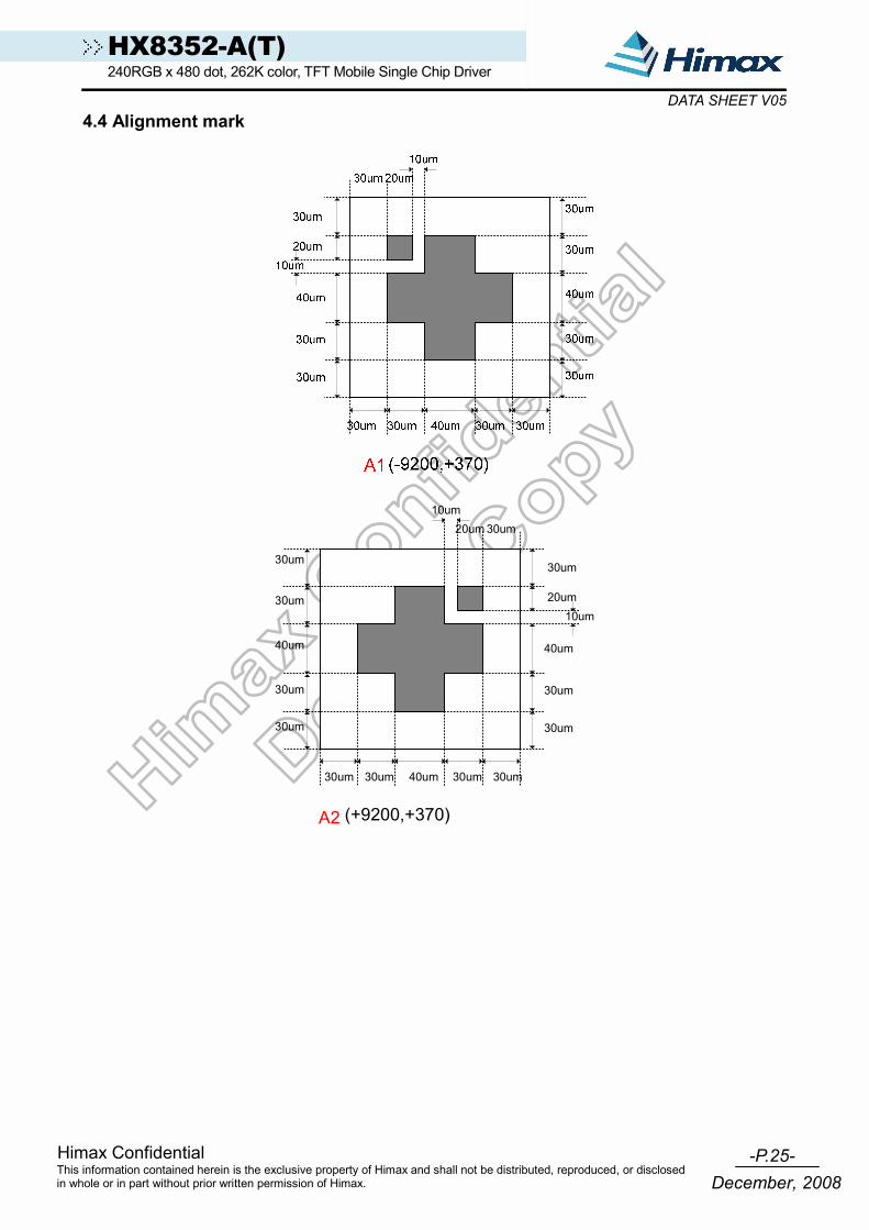
-P.25- Himax Confidential
December, 2008This information contained herein is the exclusive property of Himax and shall not be distributed, reproduced, or disclosed in whole or in part without prior written permission of Himax.
HX8352-A(T) 240RGB x 480 dot, 262K color, TFT Mobile Single Chip Driver
DATA SHEET V054.4 Alignment mark
(+9200,+370)A2
30um30um40um30um30um
30um
30um
40um
10um20um
30um
30um
30um
40um
30um
30um
30um20um10um
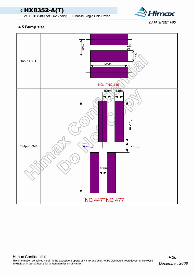
-P.26- Himax Confidential
December, 2008This information contained herein is the exclusive property of Himax and shall not be distributed, reproduced, or disclosed in whole or in part without prior written permission of Himax.
HX8352-A(T) 240RGB x 480 dot, 262K color, TFT Mobile Single Chip Driver
DATA SHEET V054.5 Bump size
Input PAD 16um
40um
24um
120um
NO.1~NO.446
Output PAD
16um 14um
18um
NO.447~NO.477

-P.27- Himax Confidential
December, 2008This information contained herein is the exclusive property of Himax and shall not be distributed, reproduced, or disclosed in whole or in part without prior written permission of Himax.
HX8352-A(T) 240RGB x 480 dot, 262K color, TFT Mobile Single Chip Driver
DATA SHEET V05
14um
14um
106um16um
228um
14um
NO.700~NO.1453

-P.28- Himax Confidential
December, 2008This information contained herein is the exclusive property of Himax and shall not be distributed, reproduced, or disclosed in whole or in part without prior written permission of Himax.
HX8352-A(T) 240RGB x 480 dot, 262K color, TFT Mobile Single Chip Driver
DATA SHEET V0516um 14um
18um
NO.1676~NO.1706

-P.29- Himax Confidential
December, 2008This information contained herein is the exclusive property of Himax and shall not be distributed, reproduced, or disclosed in whole or in part without prior written permission of Himax.
HX8352-A(T) 240RGB x 480 dot, 262K color, TFT Mobile Single Chip Driver
DATA SHEET V05
5. Function Description 5.1 Interface control mode
The HX8352-A supports four-type interface mode: Command-Parameter interface mode, Register-Content interface mode, RGB interface mode. Command-Parameter interface mode, Register-Content interface mode are selected by the external pins IFSEL0, BS2-0 setting as shown in Table5.1. There are two-type chip access formats in HX8352-A. One is register command for chip internal operation. The other is display data for chip display.
IFSEL0 BS2-0 Register Data Display Data
0 000, 001, 010, 011, 100, 101, 110
Command-Parameter interface (MPU interface) GRAM
0 111 Command-Parameter interface (SPI + RGB interface) Normal: RGB interface
1 000, 001, 010, 011, 100
Register-Content interface (MPU interface) GRAM
1 11x Register-Content interface (SPI + RGB interface) Normal: RGB interface
Table 5. 1 Interface Mode Selection There are two-type register groups in HX8352-A. One is accessed only via Command-Parameter interface. The other is accessed only via Register-Content interface. This manual description focuses on Register-Content interface mode and RGB interface mode, about the Command-Parameter interface mode; please refer to the HX8352-A(N) datasheet for detail.
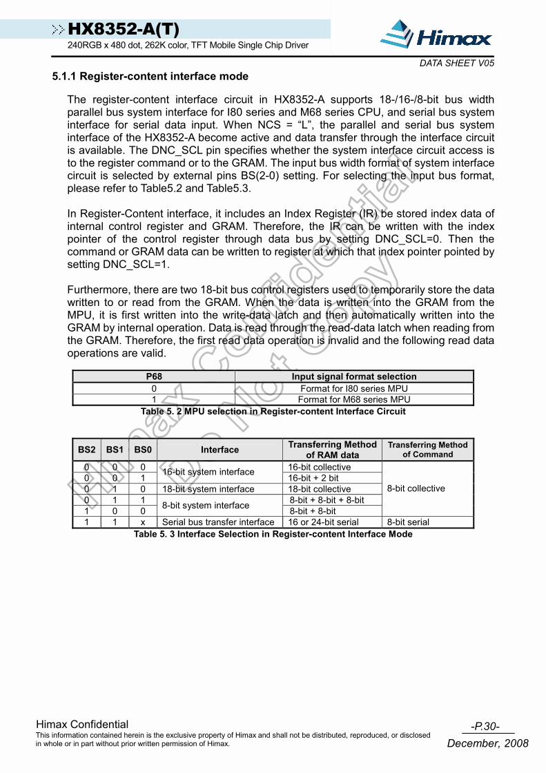
-P.30- Himax Confidential
December, 2008This information contained herein is the exclusive property of Himax and shall not be distributed, reproduced, or disclosed in whole or in part without prior written permission of Himax.
HX8352-A(T) 240RGB x 480 dot, 262K color, TFT Mobile Single Chip Driver
DATA SHEET V055.1.1 Register-content interface mode
The register-content interface circuit in HX8352-A supports 18-/16-/8-bit bus width parallel bus system interface for I80 series and M68 series CPU, and serial bus system interface for serial data input. When NCS = “L”, the parallel and serial bus system interface of the HX8352-A become active and data transfer through the interface circuit is available. The DNC_SCL pin specifies whether the system interface circuit access is to the register command or to the GRAM. The input bus width format of system interface circuit is selected by external pins BS(2-0) setting. For selecting the input bus format, please refer to Table5.2 and Table5.3. In Register-Content interface, it includes an Index Register (IR) be stored index data of internal control register and GRAM. Therefore, the IR can be written with the index pointer of the control register through data bus by setting DNC_SCL=0. Then the command or GRAM data can be written to register at which that index pointer pointed by setting DNC_SCL=1. Furthermore, there are two 18-bit bus control registers used to temporarily store the data written to or read from the GRAM. When the data is written into the GRAM from the MPU, it is first written into the write-data latch and then automatically written into the GRAM by internal operation. Data is read through the read-data latch when reading from the GRAM. Therefore, the first read data operation is invalid and the following read data operations are valid.
P68 Input signal format selection 0 Format for I80 series MPU 1 Format for M68 series MPU
Table 5. 2 MPU selection in Register-content Interface Circuit
BS2 BS1 BS0 Interface Transferring Method of RAM data
Transferring Method of Command
0 0 0 16-bit collective 0 0 1
16-bit system interface 16-bit + 2 bit
0 1 0 18-bit system interface 18-bit collective 0 1 1 8-bit + 8-bit + 8-bit 1 0 0 8-bit system interface 8-bit + 8-bit
8-bit collective
1 1 x Serial bus transfer interface 16 or 24-bit serial 8-bit serial Table 5. 3 Interface Selection in Register-content Interface Mode

-P.31- Himax Confidential
December, 2008This information contained herein is the exclusive property of Himax and shall not be distributed, reproduced, or disclosed in whole or in part without prior written permission of Himax.
HX8352-A(T) 240RGB x 480 dot, 262K color, TFT Mobile Single Chip Driver
DATA SHEET V055.1.2 Parallel bus system interface
The input / output data from data pins (DB17-0) and signal operation of the I80/M68 series parallel bus interface are listed in Table 5.2.
Operations NRD_E NWR_RNW DNC_SCL Writes Indexes into IR 0 1 0 Reads internal status 1 0 0 Writes command into register or data into GRAM 0 1 1 Reads command from register or data from GRAM 1 0 1
Table 5. 4 Data Pin Function for I80 Series CPU
Operations NRD_E NWR_RNW DNC_SCL Writes Indexes into IR 1 0 0 Reads internal status 1 1 0 Writes command into register or data into GRAM 1 0 1 Reads command from register or data from GRAM 1 1 1
Table 5. 5 Data Pin Function for M68 Series CPU
Write to the register
Read the register
NCS
DNC_SCL
NRD_E
DB7-0 Command write to the register"index" write to index register
NCS
DNC_SCL
NWR_RNW
DB7-0 Command read from the register"index" write to index register
NRD_E
NWR_RNW
Figure 5. 1 Register Read/Write Timing in Parallel Bus System Interface (for I80 Series MPU)

-P.32- Himax Confidential
December, 2008This information contained herein is the exclusive property of Himax and shall not be distributed, reproduced, or disclosed in whole or in part without prior written permission of Himax.
HX8352-A(T) 240RGB x 480 dot, 262K color, TFT Mobile Single Chip Driver
DATA SHEET V05
DNC_SCL
NWR_RND
Dummy Read Data 1 pixel data
NCS
NRD_E
"22" h
DNC_SCL
NRD_E
nth pixel ; Address = N
NCS
(n+1)th pixel ; Address = N+1
"22" h 1st write data 1st write data 1st write data 2nd write data2nd write data2nd write data
(n+2)th pixel ; Address = N+2
1st read data 2nd read data
NWR_RNW
NCS
DNC_SCL
NRD_E
NCS
DNC_SCL
NRD_E
dummy read data 1st read data
"22"h write to index register Display data write to RAM Display data write to RAM
nth pixel, Address = N (n+1) pixel, Address = N +1
NWR_RNW
"22"h
1 pixel data
NWR_RNW
DB15-0/DB17-0
DB15-0/DB17-0
DB15-0/DB17-0
DB15-0/DB17-0
Figure 5. 2 GRAM Read/Write Timing in 16-/18-Bit Parallel Bus System Interface (for I80 Series MPU)
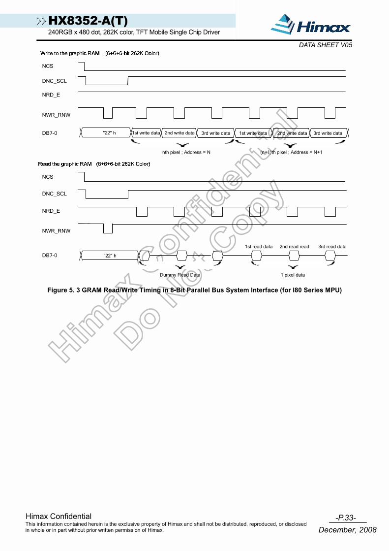
-P.33- Himax Confidential
December, 2008This information contained herein is the exclusive property of Himax and shall not be distributed, reproduced, or disclosed in whole or in part without prior written permission of Himax.
HX8352-A(T) 240RGB x 480 dot, 262K color, TFT Mobile Single Chip Driver
DATA SHEET V05
DNC_SCL
NWR_RNW
Dummy Read Data
NCS
NRD_E
"22" h
DNC_SCL
DB7-0
NWR_RNW
nth pixel ; Address = N
NCS
(n+1)th pixel ; Address = N+1
"22" h 1st write data 3rd write data 2nd write data 3rd write data1st write data2nd write data
NRD_E
DB7-0
1 pixel data
1st read data 2nd read read 3rd read data
Figure 5. 3 GRAM Read/Write Timing in 8-Bit Parallel Bus System Interface (for I80 Series MPU)

-P.34- Himax Confidential
December, 2008This information contained herein is the exclusive property of Himax and shall not be distributed, reproduced, or disclosed in whole or in part without prior written permission of Himax.
HX8352-A(T) 240RGB x 480 dot, 262K color, TFT Mobile Single Chip Driver
DATA SHEET V05
Write to the register
Read the register
NCS
DNC_SCL
NWR_RNW
DB7-0 Command write to the register"index" write to index register
NCS
DNC_SCL
NRD_E
DB7-0 Command read from the register"index" write to index register
NWR_RNW
NRD_E
Figure 5. 4 Register Read/Write Timing in Parallel Bus System Interface (for M68 Series MPU)

-P.35- Himax Confidential
December, 2008This information contained herein is the exclusive property of Himax and shall not be distributed, reproduced, or disclosed in whole or in part without prior written permission of Himax.
HX8352-A(T) 240RGB x 480 dot, 262K color, TFT Mobile Single Chip Driver
DATA SHEET V05
DNC_SCL
NRD_E
Dummy Read Data 1 pixel data
NCS
NWR_RNW
"22" h
DNC_SCL
NRD_E
nth pixel ; Address = N
NCS
(n+1)th pixel ; Address = N+1
"22" h 1st write data 1st write data 1st write data 2nd write data2nd write data2nd write data
(n+2)th pixel ; Address = N+2
1st read data 2nd read data
NWR_RNW
NCS
DNC_SCL
NWR_RNW
NCS
DNC_SCL
NWR_RNW
dummy read data 1st read data
"22"h write to index register Display data write to RAM Display data write to RAM
nth pixel, Address = N (n+1) pixel, Address = N +1
NRD_E
"22"h
1 pixel data
NRD_E
DB15-0/DB17-0
DB15-0/DB17-0
DB15-0/DB17-0
DB15-0/DB17-0
Figure 5. 5 GRAM Read/Write Timing in 16-/18-Bit Parallel Bus System Interface (for M68 Series MPU)
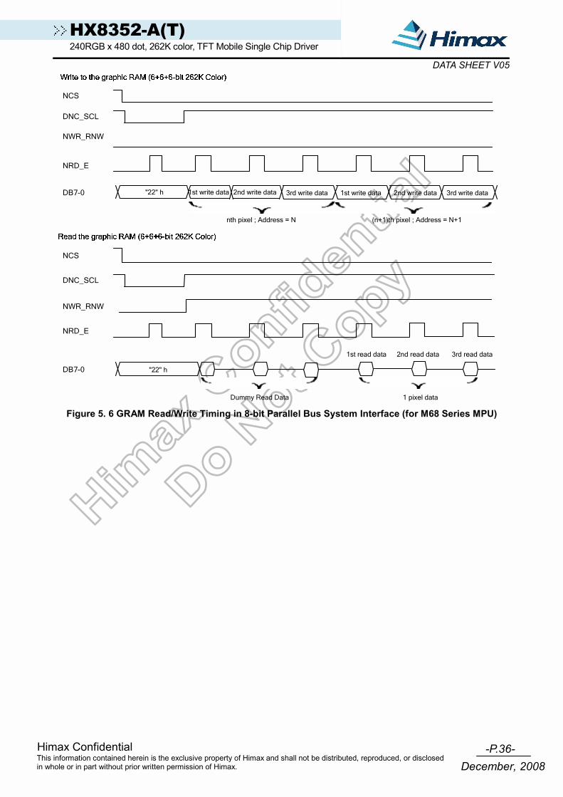
-P.36- Himax Confidential
December, 2008This information contained herein is the exclusive property of Himax and shall not be distributed, reproduced, or disclosed in whole or in part without prior written permission of Himax.
HX8352-A(T) 240RGB x 480 dot, 262K color, TFT Mobile Single Chip Driver
DATA SHEET V05
DNC_SCL
NRD_E
Dummy Read Data
NCS
NWR_RNW
"22" h
DNC_SCL
DB7-0
NRD_E
nth pixel ; Address = N
NCS
(n+1)th pixel ; Address = N+1
"22" h 1st write data 3rd write data 2nd write data 3rd write data1st write data2nd write data
NWR_RNW
DB7-0
1 pixel data
1st read data 2nd read data 3rd read data
Figure 5. 6 GRAM Read/Write Timing in 8-bit Parallel Bus System Interface (for M68 Series MPU)

-P.37- Himax Confidential
December, 2008This information contained herein is the exclusive property of Himax and shall not be distributed, reproduced, or disclosed in whole or in part without prior written permission of Himax.
HX8352-A(T) 240RGB x 480 dot, 262K color, TFT Mobile Single Chip Driver
DATA SHEET V0518-bit Parallel bus system interface The I80-system 18-bit parallel bus interface in command-parameter interface mode can be used by setting external pins “P68, BS2, BS1, BS0” pins to “0010”. And the M68-system 18-bit parallel bus interface in command-parameter interface mode can be used by setting “P68, BS2, BS1, and BS0” pins to “1010”. Figure 5.7 is the example of interface with I80/M68 microcomputer system interface.
Figure 5. 7 Example of I80- / M68- System 16-Bit Parallel Bus Interface
Figure 5. 8 Input Data Bus and GRAM Data Mapping in 18-Bit Bus System Interface
(“BS2, BS1, BS0”=”010”)
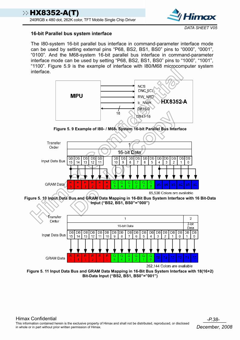
-P.38- Himax Confidential
December, 2008This information contained herein is the exclusive property of Himax and shall not be distributed, reproduced, or disclosed in whole or in part without prior written permission of Himax.
HX8352-A(T) 240RGB x 480 dot, 262K color, TFT Mobile Single Chip Driver
DATA SHEET V0516-bit Parallel bus system interface The I80-system 16-bit parallel bus interface in command-parameter interface mode can be used by setting external pins “P68, BS2, BS1, BS0” pins to “0000”, “0001”, “0100”. And the M68-system 16-bit parallel bus interface in command-parameter interface mode can be used by setting “P68, BS2, BS1, BS0” pins to “1000”, “1001”, “1100”. Figure 5.9 is the example of interface with I80/M68 microcomputer system interface.
Figure 5. 9 Example of I80- / M68- System 16-bit Parallel Bus Interface
Figure 5. 10 Input Data Bus and GRAM Data Mapping in 16-Bit Bus System Interface with 16 Bit-Data
Input (“BS2, BS1, BS0”=”000”)
Figure 5. 11 Input Data Bus and GRAM Data Mapping in 16-Bit Bus System Interface with 18(16+2)
Bit-Data Input (“BS2, BS1, BS0”=”001”)

-P.39- Himax Confidential
December, 2008This information contained herein is the exclusive property of Himax and shall not be distributed, reproduced, or disclosed in whole or in part without prior written permission of Himax.
HX8352-A(T) 240RGB x 480 dot, 262K color, TFT Mobile Single Chip Driver
DATA SHEET V058-bit Parallel bus system interface The I80-system 8-bit parallel bus interface in register-content interface mode can be used by setting external pins “P68, BS2, BS1, BS0” pins to “0011” or “0100”. And the M68-system 8-bit parallel bus interface in command-parameter interface mode can be used by setting “P68, BS2, BS1, BS0” pins to “1011” or “0100”. Figure 5.13~16 are the example of interface with I80/M68 microcomputer system interface.
Figure 5. 12 Example of I80- / M68- System 8-Bit Parallel Bus Interface
Figure 5. 13 Input Data Bus and GRAM Data Mapping in 8-Bit Bus System Interface with 18( 6 + 6 + 6 )
Bit-Data Input (“BS2, BS1, BS0”=”011”)
Figure 5. 14 Input Data Bus and GRAM Data Mapping in 8-Bit Bus System Interface with 16(5 + 6 + 5) Bit-Data Input (“BS2, BS1, BS0”=”100”)

-P.40- Himax Confidential
December, 2008This information contained herein is the exclusive property of Himax and shall not be distributed, reproduced, or disclosed in whole or in part without prior written permission of Himax.
HX8352-A(T) 240RGB x 480 dot, 262K color, TFT Mobile Single Chip Driver
DATA SHEET V055.1.3 Serial bus system interface
The HX8352-A supports the serial bus interface in register-content mode by setting external pins “BS2, BS1” pins to “11”. The serial bus system interface mode is enabled through the chip select line (NCS), and it is accessed via a control consisting of the serial input data (SDI), serial output data (SDO) and the serial transfer clock signal (DNC_SCL).
As the chip select signal (NCS) goes low, the start byte needs to be transferred first. The start byte is made up of 6-bit bus device identification code; register select (RS) bit and read/write operation (RW) bit. The five upper bits of 6-bit bus device identification code must be set to “01110”, and the least significant bit of the identification code must be set as the external pin BS0 input as “ID”.
The seventh bit (RS) of the start byte determines internal index register or register, GRAM accessing. RS must be set to “0” when writing data to the index register or reading the status and it must be set to “1” when writing or reading a command or GRAM data. The read or write operation is selected by the eighth bit (RW) of the start byte. The data is written to the chip when R/W = 0, and read from chip when RW = 1.
RS RW Function 0 0 Writes Indexes into IR 1 0 Writes command into register or data into GRAM 1 1 Reads command from register or data from GRAM
Table 5. 6 The Function of RS and R/W Bit bus

-P.41- Himax Confidential
December, 2008This information contained herein is the exclusive property of Himax and shall not be distributed, reproduced, or disclosed in whole or in part without prior written permission of Himax.
HX8352-A(T) 240RGB x 480 dot, 262K color, TFT Mobile Single Chip Driver
DATA SHEET V05
Figure 5. 15 Data Write Timing in Serial Bus System Interface
Figure 5. 16 Data Write Timing in Serial Bus System Interface
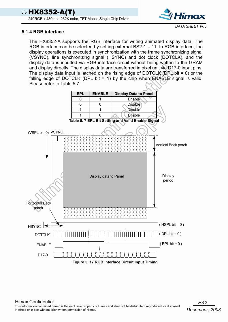
-P.42- Himax Confidential
December, 2008This information contained herein is the exclusive property of Himax and shall not be distributed, reproduced, or disclosed in whole or in part without prior written permission of Himax.
HX8352-A(T) 240RGB x 480 dot, 262K color, TFT Mobile Single Chip Driver
DATA SHEET V055.1.4 RGB interface
The HX8352-A supports the RGB interface for writing animated display data. The RGB interface can be selected by setting external BS2-1 = 11. In RGB interface, the display operations is executed in synchronization with the frame synchronizing signal (VSYNC), line synchronizing signal (HSYNC) and dot clock (DOTCLK), and the display data is inputted via RGB interface circuit without being written to the GRAM and display directly. The display data are transferred in pixel unit via D17-0 input pins. The display data input is latched on the rising edge of DOTCLK (DPL bit = 0) or the falling edge of DOTCLK (DPL bit = 1) by the chip when ENABLE signal is valid. Please refer to Table 5.7.
EPL ENABLE Display Data to Panel
0 1 Enable 0 0 Disable 1 1 Disable 1 0 Enable
Table 5. 7 EPL Bit Setting and Valid Enable Signal
Display period
HSYNC
VSYNC
DOTCLK
( EPL bit = 0 )
Display data to Panel
( DPL bit = 0 )
( HSPL bit = 0 )
(VSPL bit=0)
ENABLE
D17-0
Vertical Back porch
Horizontal Back porch
Figure 5. 17 RGB Interface Circuit Input Timing
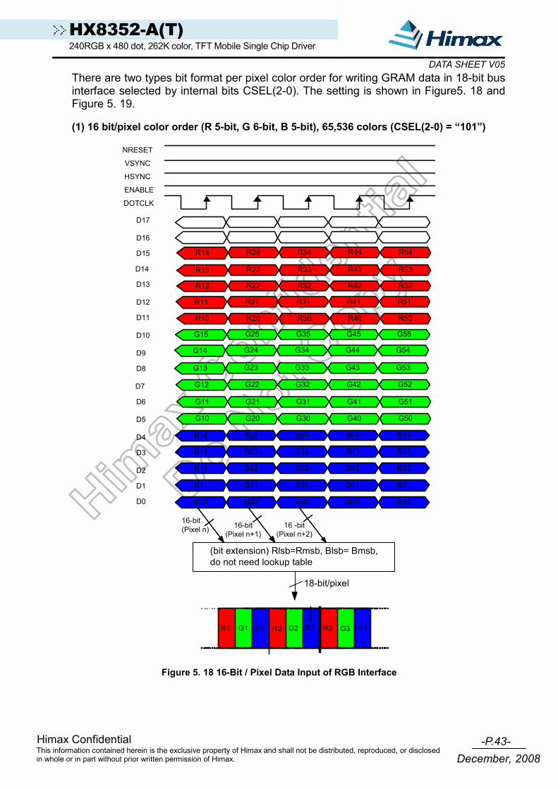
-P.43- Himax Confidential
December, 2008This information contained herein is the exclusive property of Himax and shall not be distributed, reproduced, or disclosed in whole or in part without prior written permission of Himax.
HX8352-A(T) 240RGB x 480 dot, 262K color, TFT Mobile Single Chip Driver
DATA SHEET V05There are two types bit format per pixel color order for writing GRAM data in 18-bit bus interface selected by internal bits CSEL(2-0). The setting is shown in Figure5. 18 and Figure 5. 19.
(1) 16 bit/pixel color order (R 5-bit, G 6-bit, B 5-bit), 65,536 colors (CSEL(2-0) = “101”)
NRESET
VSYNC
HSYNC
ENABLE
DOTCLK
D13
D17
D16
D15
D14
D12
D11
D9
D8
D7
D6
D5
D10
D4
D3
D2
D1
D0
16-bit(Pixel n) 16-bit
(Pixel n+1)16 -bit
(Pixel n+2)
R1 G1 B1 R2 G2 B2 R3 G3 B3
18-bit/pixel
R10 R20 R30 R40 R50
R14 R24 R34 R44 R54
R13 R23 R33 R43 R53
R12 R22 R32 R42 R52
R11 R21 R31 R41 R51
G15 G25 G35 G45 G55
G12 G22 G32 G42 G52
G11 G21 G31 G41 G51
G10 G20 G30 G40 G50
B14 B24 B34 B44 B54
G13 G23 G33 G43 G53
G14 G24 G34 G44 G54
B13 B23 B33 B43 B53
B12 B22 B32 B42 B52
B11 B21 B31 B41 B51
B10 B20 B30 B40 B50
(bit extension) Rlsb=Rmsb, Blsb= Bmsb, do not need lookup table
Figure 5. 18 16-Bit / Pixel Data Input of RGB Interface

-P.44- Himax Confidential
December, 2008This information contained herein is the exclusive property of Himax and shall not be distributed, reproduced, or disclosed in whole or in part without prior written permission of Himax.
HX8352-A(T) 240RGB x 480 dot, 262K color, TFT Mobile Single Chip Driver
DATA SHEET V05(2) 18 bit/pixel color order (R 6-bit, G 6-bit, B 6-bit), 262,144 colors (CSEL(2-0) = “110”)
NRESET
VSYNC
HSYNC
ENABLE
DOTCLK
R11 R21 R31 R41 R51
R10 R20 R30 R40 R50
G15 G25 G35 G45 G55
D13
D12
D11
G12 G22 G32 G42 G52
G11 G21 G31 G41 G51
G10 G20 G30 G40 G50
B15 B25 B35 B45 B55
G13 G23 G33 G43 G53D9
D8
D7
D6
D5
G14 G24 G34 G44 G54D10
B14 B24 B34 B44 B54
B13 B23 B33 B43 B53
B12 B22 B32 B42 B52
B11 B21 B31 B41 B51
D4
D3
D2
D1
D0 B10 B20 B30 B40 B50
18-bit(Pixel n)
R15 R25 R35 R45 R55
R14 R24 R34 R44 R54
R13 R23 R33 R43 R53
D17
D16
D15
R12 R22 R32 R42 R52D14
18-bit(Pixel n+1)
18-bit(Pixel n+2)
R1 G1 B1 R2 G2 B2 R3 G3 B3
Figure 5. 19 18-Bit / Pixel Data Input of RGB Interface
-P.45- Himax Confidential
December, 2008This information contained herein is the exclusive property of Himax and shall not be distributed, reproduced, or disclosed in whole or in part without prior written permission of Himax.
HX8352-A(T) 240RGB x 480 dot, 262K color, TFT Mobile Single Chip Driver
DATA SHEET V055.2 Address counter (AC)
The HX8352-A contains an address counter (AC) which assigns address for writing/reading pixel data to/from GRAM. The address pointers set the position of GRAM whose addresses range:
RES_SEL1 RES_SEL0 X Range Y Range Panel Resolution 0 0 0~239d 0~319d. 240RGB x320 dot 0 1 0~239d 0~399d. 240RGB x400 dot 1 0 0~239d 0~431d. 240RGB x432 dot 1 1 0~239d 0~479d. 240RGB x480 dot
Table 5. 8 Addresses Counter Range
Every time when a pixel data is written into the GRAM, the X address or Y address of AC will be automatically increased by 1 (or decreased by 1), which is decided by the register (MV, MX and MY bit) setting. To simplify the address control of GRAM access, the window address function allows for writing data only to a window area of GRAM specified by registers. After data is written to the GRAM, the AC will be increased or decreased within setting window address-range which is specified by the Column address register (start: SC, end: EC) or the Row address register (start: SP, end: EP). Therefore, the data can be written consecutively without thinking a data wrap by those bit function.

-P.46- Himax Confidential
December, 2008This information contained herein is the exclusive property of Himax and shall not be distributed, reproduced, or disclosed in whole or in part without prior written permission of Himax.
HX8352-A(T) 240RGB x 480 dot, 262K color, TFT Mobile Single Chip Driver
DATA SHEET V055.2.1 MCU to memory write/read direction
B
E
Data stream from MCU is likethis figure
Figure 5. 20 MCU to Memory Write/Read Direction
The data is written in the order as illustrated above. The counter that dictates which physical memory the data is to be written is controlled by “Memory Access Control” Command, Bits MY, MX, MV as described below.
MY
MX
MV
Phy
sica
lR
owP
oint
er
Figure 5. 21 MY, MX, MV Setting of 240RGB x 432 Dot
MV MX MY CASET PASET 0 0 0 Direct to Physical Column Pointer Direct to Physical Row Pointer 0 0 1 Direct to Physical Column Pointer Direct to (431-Physical Row Pointer) with SC 0 1 0 Direct to (239-Physical Column Pointer) Direct to Physical Row Pointer 0 1 1 Direct to (239-Physical Column Pointer) Direct to (431-Physical Row Pointer) 1 0 0 Direct to Physical Row Pointer Direct to Physical Column Pointer 1 0 1 Direct to (431-Physical Row Pointer) Direct to Physical Column Pointer 1 1 0 Direct to Physical Row Pointer Direct to (239-Physical Column Pointer) 1 1 1 Direct to (431-Physical Row Pointer) Direct to (239-Physical Column Pointer)
Table 5. 9 MY, MX, MV Setting of 240RGB x 432 Dot

-P.47- Himax Confidential
December, 2008This information contained herein is the exclusive property of Himax and shall not be distributed, reproduced, or disclosed in whole or in part without prior written permission of Himax.
HX8352-A(T) 240RGB x 480 dot, 262K color, TFT Mobile Single Chip Driver
DATA SHEET V05The following figure depicts the update method set by MV, MX and MY bit.
Memory Access Control Display Data
Direction MV MX MY
Image in the Host Image in the Driver (GRAM)
Normal 0 0 0
B
E
Y-Mirror 0 0 1
B
E
X,Y address (0,0)X: CASETY: RASET B
EH/W Position (0,0)
X-Mirror 0 1 0
B
E
X-Mirror Y-Mirror 0 1 1
B
E
X-Y Exchange 1 0 0
B
E
X,Y address (0,0)X: CASETY: RASET
B
E
H/W Position (0,0)
X-Y Exchange Y-Mirror
1 0 1
B
E
X,Y address (0,0)X: CASETY: RASET
H/W Position (0,0)
B
E
X-Y Exchange X-Mirror
1 1 0
B
E
X,Y address (0,0)X: CASETY: RASET
H/W Position (0,0) B
E
X-Y Exchange X-Mirror Y-Mirror
1 1 1
B
E
X,Y address (0,0)X: CASETY: RASET
H/W Position (0,0)
B
E
Figure 5. 22 Address Direction Settings
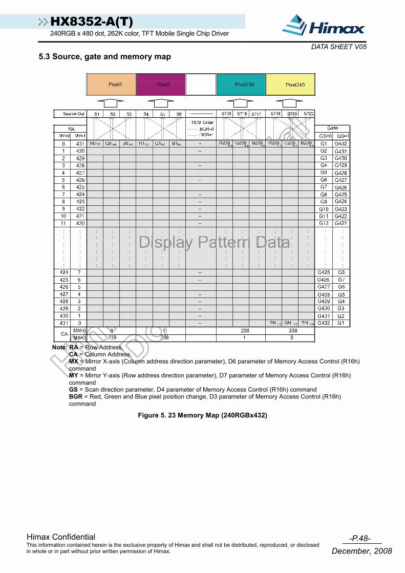
-P.48- Himax Confidential
December, 2008This information contained herein is the exclusive property of Himax and shall not be distributed, reproduced, or disclosed in whole or in part without prior written permission of Himax.
HX8352-A(T) 240RGB x 480 dot, 262K color, TFT Mobile Single Chip Driver
DATA SHEET V055.3 Source, gate and memory map
Note: RA = Row Address,
CA = Column Address, MX = Mirror X-axis (Column address direction parameter), D6 parameter of Memory Access Control (R16h) command MY = Mirror Y-axis (Row address direction parameter), D7 parameter of Memory Access Control (R16h) command GS = Scan direction parameter, D4 parameter of Memory Access Control (R16h) command BGR = Red, Green and Blue pixel position change, D3 parameter of Memory Access Control (R16h) command
Figure 5. 23 Memory Map (240RGBx432)
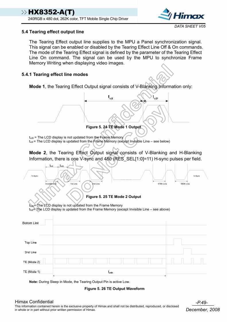
-P.49- Himax Confidential
December, 2008This information contained herein is the exclusive property of Himax and shall not be distributed, reproduced, or disclosed in whole or in part without prior written permission of Himax.
HX8352-A(T) 240RGB x 480 dot, 262K color, TFT Mobile Single Chip Driver
DATA SHEET V055.4 Tearing effect output line
The Tearing Effect output line supplies to the MPU a Panel synchronization signal. This signal can be enabled or disabled by the Tearing Effect Line Off & On commands. The mode of the Tearing Effect signal is defined by the parameter of the Tearing Effect Line On command. The signal can be used by the MPU to synchronize Frame Memory Writing when displaying video images.
5.4.1 Tearing effect line modes
Mode 1, the Tearing Effect Output signal consists of V-Blanking Information only:
Figure 5. 24 TE Mode 1 Output
tvdh = The LCD display is not updated from the Frame Memory tvdl = The LCD display is updated from the Frame Memory (except Invisible Line – see below) Mode 2, the Tearing Effect Output signal consists of V-Blanking and H-Blanking Information, there is one V-sync and 480 (RES_SEL[1:0]=11) H-sync pulses per field.
Figure 5. 25 TE Mode 2 Output
thdh= The LCD display is not updated from the Frame Memory thdl= The LCD display is updated from the Frame Memory (except Invisible Line – see above)
Note: During Sleep in Mode, the Tearing Output Pin is active Low.
Figure 5. 26 TE Output Waveform
V - Sync
Invisible Line 1 st Line 2 nd Line
t hdl t hdh
V-Sync
479th Line 480th Line
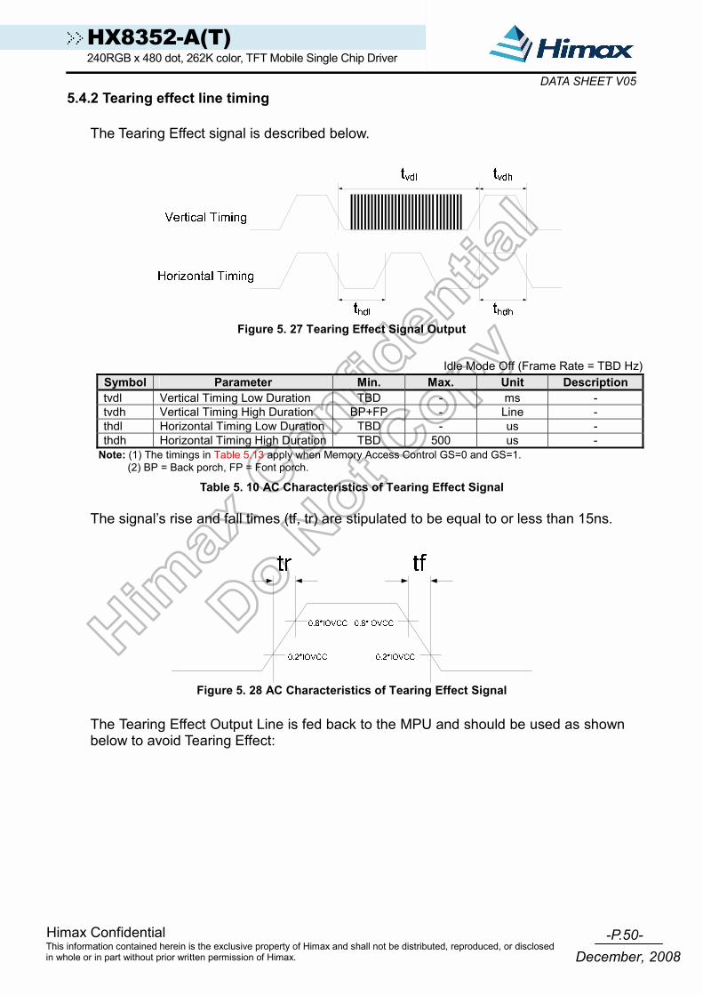
-P.50- Himax Confidential
December, 2008This information contained herein is the exclusive property of Himax and shall not be distributed, reproduced, or disclosed in whole or in part without prior written permission of Himax.
HX8352-A(T) 240RGB x 480 dot, 262K color, TFT Mobile Single Chip Driver
DATA SHEET V055.4.2 Tearing effect line timing
The Tearing Effect signal is described below.
Figure 5. 27 Tearing Effect Signal Output
Idle Mode Off (Frame Rate = TBD Hz)
Symbol Parameter Min. Max. Unit Description tvdl Vertical Timing Low Duration TBD - ms - tvdh Vertical Timing High Duration BP+FP - Line - thdl Horizontal Timing Low Duration TBD - us - thdh Horizontal Timing High Duration TBD 500 us -
Note: (1) The timings in Table 5.13 apply when Memory Access Control GS=0 and GS=1. (2) BP = Back porch, FP = Font porch.
Table 5. 10 AC Characteristics of Tearing Effect Signal The signal’s rise and fall times (tf, tr) are stipulated to be equal to or less than 15ns.
Figure 5. 28 AC Characteristics of Tearing Effect Signal
The Tearing Effect Output Line is fed back to the MPU and should be used as shown below to avoid Tearing Effect:

-P.51- Himax Confidential
December, 2008This information contained herein is the exclusive property of Himax and shall not be distributed, reproduced, or disclosed in whole or in part without prior written permission of Himax.
HX8352-A(T) 240RGB x 480 dot, 262K color, TFT Mobile Single Chip Driver
DATA SHEET V05Example 1: MPU write is faster than panel read
Figure 5. 29
Data write to Frame Memory is now synchronized to the Panel Scan. It should be written during the vertical sync pulse of the Tearing Effect Output Line. This ensures that data is always written ahead of the panel scan and each Panel Frame refresh has a complete new image:
Figure 5. 30

-P.52- Himax Confidential
December, 2008This information contained herein is the exclusive property of Himax and shall not be distributed, reproduced, or disclosed in whole or in part without prior written permission of Himax.
HX8352-A(T) 240RGB x 480 dot, 262K color, TFT Mobile Single Chip Driver
DATA SHEET V05Example 2: MPU write is slower than panel read
Time
Time
Time
MCU to Memory
TE output signal
Memory to LCD
Image on LCD a b c d1st 320th
1st 320th
e f
Figure 5. 31
The MPU to Frame Memory write begins just after Panel Read has commenced i.e. after one horizontal sync pulse of the Tearing Effect Output Line. This allows time for the image to download behind the Panel Read pointer and finishing download during the subsequent Frame before the Read Pointer “catches” the MPU to Frame memory write position.
Figure 5. 32

-P.53- Himax Confidential
December, 2008This information contained herein is the exclusive property of Himax and shall not be distributed, reproduced, or disclosed in whole or in part without prior written permission of Himax.
HX8352-A(T) 240RGB x 480 dot, 262K color, TFT Mobile Single Chip Driver
DATA SHEET V055.5 Oscillator
The HX8352-A can oscillate an internal R-C oscillator with an internal oscillation resistor (Rf). The oscillation frequency is changed according to the RADJ[3:0] internal register. Please refer to OSC control register (R17h). The default frequency is 7.5MHz.
Figure 5. 33 Oscillation Circuit 5.6 Source driver
The HX8352-A contains a 720 channels of source driver (S1~S720) which is used for driving the source line of TFT LCD panel. The source driver converts the digital data from GRAM into the analog voltage for 720 channels and generates corresponding gray scale voltage output, which can realize a 262K colors display simultaneously. Since the output circuit of this source driver incorporates an operational amplifier, a positive and a negative voltage can be alternately outputted from each channel.
5.7 Gate driver
The HX8352-A contains a 480 gate channels of gate driver (G1~G480) which is used for driving the gate. The gate driver level is VGH when scan some line, VGL the other lines.
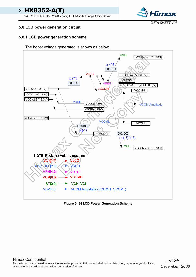
-P.54- Himax Confidential
December, 2008This information contained herein is the exclusive property of Himax and shall not be distributed, reproduced, or disclosed in whole or in part without prior written permission of Himax.
HX8352-A(T) 240RGB x 480 dot, 262K color, TFT Mobile Single Chip Driver
DATA SHEET V055.8 LCD power generation circuit 5.8.1 LCD power generation scheme
The boost voltage generated is shown as below.
VSSA, VSSD (0V)
VREG1 (3.5 ~ (VLCD-0.5)V)
VCOMH
VGH(4 VCI ~ 6 VCI)
VCOML
VCL
VGH
x 2~3
x (-1)
VCI (2.3 ~ 3.3V)
VLCD (4.6V ~ 6.0V)VLCD
VREG3
VBGP(1.25V)
x 4~6
VDDD(1.8V)
VGL(-5 VCI ~ -3 VCI)
DC/DC
DC/DC
DC/DC
DC/DCx (-3)~(-5)
VGL
VCOML
VCOMH
VDDDVCOM Amplitude
VREG1
IOVCC (1.65 ~ 3.3V)
VCC (2.3 ~ 3.3V)
Figure 5. 34 LCD Power Generation Scheme

-P.55- Himax Confidential
December, 2008This information contained herein is the exclusive property of Himax and shall not be distributed, reproduced, or disclosed in whole or in part without prior written permission of Himax.
HX8352-A(T) 240RGB x 480 dot, 262K color, TFT Mobile Single Chip Driver
DATA SHEET V055.8.2 Various boosting steps
The boost steps of each boosting voltage are selected according to how the external capacitors are connected. Different booster applications are shown as below.
VLCD=2xVCI
VCL=-1xVCI
VGH=6xVCIVGL=-5xVCI
VLCD
VCLC12A
C12B
C21A
C21B
C22A
C22B
VGH
VGL
C11A
C11B
Figure 5. 35 Various Boosting Steps

-P.56- Himax Confidential
December, 2008This information contained herein is the exclusive property of Himax and shall not be distributed, reproduced, or disclosed in whole or in part without prior written permission of Himax.
HX8352-A(T) 240RGB x 480 dot, 262K color, TFT Mobile Single Chip Driver
DATA SHEET V055.9 Gamma adjustment
The HX8352-A offers two kinds of Gamma adjustment ways to come to accord with LC characteristic, one kind is through Source Driver directly, another one is adjusted by the digital gamma correction. The Gamma adjustment way is select by internal register DGC_EN bit.
R,G,BGamma
correction(LUT)
Dithering Source Driver
8 66
Gamma register
Gary-scale of R
lum
inan
ce o
f R
Gary-scale of G
lum
inan
ce o
f G
Gary-scale of B
lum
inan
ce o
f B
Gary-scale of R
lum
inan
ce o
f R
Gary-scale of G
lum
inan
ce o
f G
Gary-scale of B
lum
inan
ce o
f B
B) Gamma adjustment of Digital Gamma Correction
Source Driver
6
Gamma register
Gary-scale of R
lum
inan
ce o
f R
Gary-scale of G
lum
inan
ce o
f G
Gary-scale of B
lum
inan
ce o
f B
Gary-scale of Whitelu
min
ance
of W
hite
A) Gamma adjustment of Source Driver
Figure 5. 36 Gamma Adjustments Different of Source Driver with Digital Gamma Correction
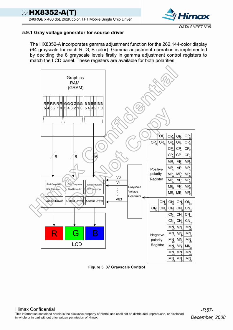
-P.57- Himax Confidential
December, 2008This information contained herein is the exclusive property of Himax and shall not be distributed, reproduced, or disclosed in whole or in part without prior written permission of Himax.
HX8352-A(T) 240RGB x 480 dot, 262K color, TFT Mobile Single Chip Driver
DATA SHEET V055.9.1 Gray voltage generator for source driver
The HX8352-A incorporates gamma adjustment function for the 262,144-color display (64 grayscale for each R, G, B color). Gamma adjustment operation is implemented by deciding the 8 grayscale levels firstly in gamma adjustment control registers to match the LCD panel. These registers are available for both polarities.
GrayscaleVoltageGenerator
6-bit Grayscale
D/A Converter
Output Driver Output Driver Output Driver
6-bit Grayscale
D/A Converter
6-bit Grayscale
D/A Converter
R G BLCD
V0V1
V63
GraphicsRAM
(GRAM)
602 01 00
12 11
01 00
1012 11OP14 OP13
0304
PositivepolarityRegister
OP OP
OPOP OP
OPOP
02 01 00
12 11 10
22 21 20
32 31 30
42 41 40
52 51 50
10
MP MP MP
MP MP MP
MP MP MP
CP CP CP
CP CP CP
MP MP MP
MP MP MP
MP MP MP
NegativepolarityRegistre
02 01 00
12 11 10
01 00
1012 11ON
14
02
MN
MN
MN
MN
MN
MN
CN
CN
ON
ON
MN
MNMN
MN
MN
MN
CN
CN
ON
ON
MN
MN
MN
MN
MN
MN
CN
CN
ON
ON
ON
ON
02 01 00
12 11 10
22 21 20
32 31 30
42 41 40
52 51 50
13
03
6 6
B3
B2
B1
B0
G5
G3
G2
G1
G0
G4
B5
B4
R5
R3
R2
R1
R0
R4
Figure 5. 37 Grayscale Control

-P.58- Himax Confidential
December, 2008This information contained herein is the exclusive property of Himax and shall not be distributed, reproduced, or disclosed in whole or in part without prior written permission of Himax.
HX8352-A(T) 240RGB x 480 dot, 262K color, TFT Mobile Single Chip Driver
DATA SHEET V055.9.1.1 Structure of grayscale voltage generator
Eight reference gamma voltages VgP/N(0, 1, 8, 20, 43, 55, 62, 63) for positive and negative polarity are specified by the center adjustment, the micro adjustment and the offset adjustment registers firstly. With those eight voltage injected into specified node of grayscale voltage generator, totally 64 grayscale voltages (V0-V63) can be generated from grayscale amplifier for LCD panel.
Gam
ma
Res
iste
rStre
am
Figure 5. 38 Structure of Grayscale Voltage Generator
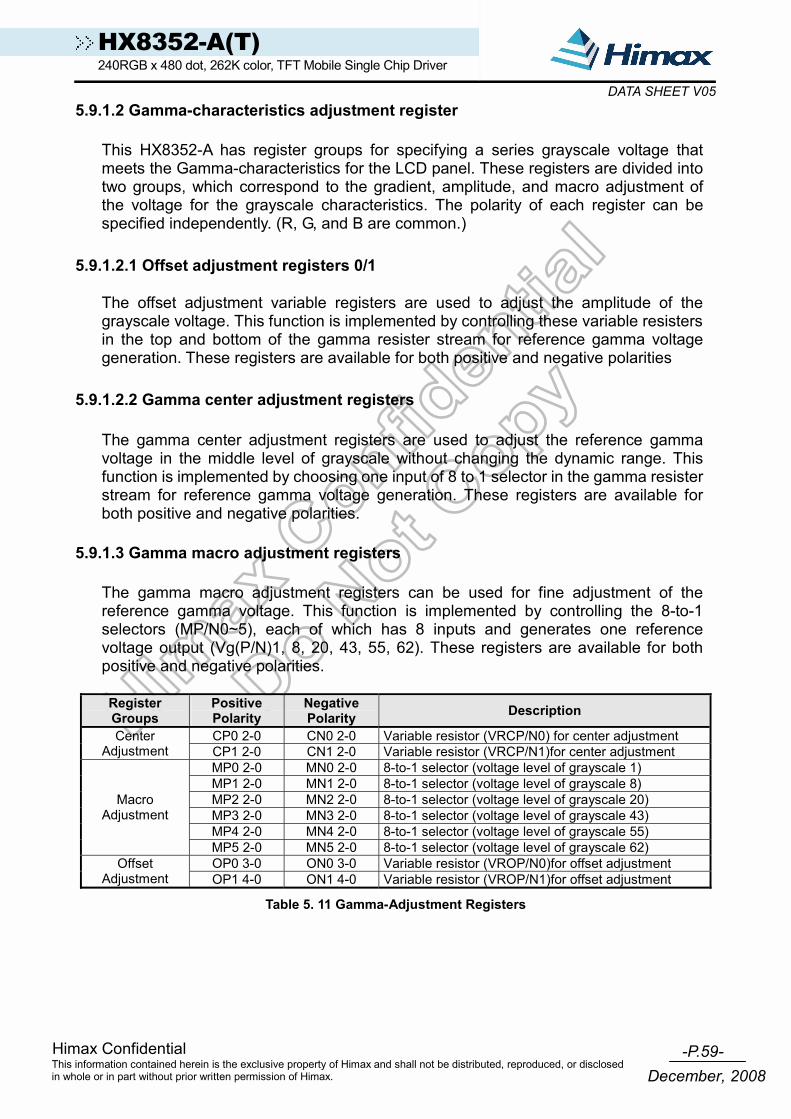
-P.59- Himax Confidential
December, 2008This information contained herein is the exclusive property of Himax and shall not be distributed, reproduced, or disclosed in whole or in part without prior written permission of Himax.
HX8352-A(T) 240RGB x 480 dot, 262K color, TFT Mobile Single Chip Driver
DATA SHEET V055.9.1.2 Gamma-characteristics adjustment register
This HX8352-A has register groups for specifying a series grayscale voltage that meets the Gamma-characteristics for the LCD panel. These registers are divided into two groups, which correspond to the gradient, amplitude, and macro adjustment of the voltage for the grayscale characteristics. The polarity of each register can be specified independently. (R, G, and B are common.)
5.9.1.2.1 Offset adjustment registers 0/1 The offset adjustment variable registers are used to adjust the amplitude of the grayscale voltage. This function is implemented by controlling these variable resisters in the top and bottom of the gamma resister stream for reference gamma voltage generation. These registers are available for both positive and negative polarities
5.9.1.2.2 Gamma center adjustment registers
The gamma center adjustment registers are used to adjust the reference gamma voltage in the middle level of grayscale without changing the dynamic range. This function is implemented by choosing one input of 8 to 1 selector in the gamma resister stream for reference gamma voltage generation. These registers are available for both positive and negative polarities.
5.9.1.3 Gamma macro adjustment registers
The gamma macro adjustment registers can be used for fine adjustment of the reference gamma voltage. This function is implemented by controlling the 8-to-1 selectors (MP/N0~5), each of which has 8 inputs and generates one reference voltage output (Vg(P/N)1, 8, 20, 43, 55, 62). These registers are available for both positive and negative polarities. Register Groups
Positive Polarity
Negative Polarity Description
CP0 2-0 CN0 2-0 Variable resistor (VRCP/N0) for center adjustment Center Adjustment CP1 2-0 CN1 2-0 Variable resistor (VRCP/N1)for center adjustment
MP0 2-0 MN0 2-0 8-to-1 selector (voltage level of grayscale 1) MP1 2-0 MN1 2-0 8-to-1 selector (voltage level of grayscale 8) MP2 2-0 MN2 2-0 8-to-1 selector (voltage level of grayscale 20) MP3 2-0 MN3 2-0 8-to-1 selector (voltage level of grayscale 43) MP4 2-0 MN4 2-0 8-to-1 selector (voltage level of grayscale 55)
Macro Adjustment
MP5 2-0 MN5 2-0 8-to-1 selector (voltage level of grayscale 62) OP0 3-0 ON0 3-0 Variable resistor (VROP/N0)for offset adjustment Offset
Adjustment OP1 4-0 ON1 4-0 Variable resistor (VROP/N1)for offset adjustment
Table 5. 11 Gamma-Adjustment Registers

-P.60- Himax Confidential
December, 2008This information contained herein is the exclusive property of Himax and shall not be distributed, reproduced, or disclosed in whole or in part without prior written permission of Himax.
HX8352-A(T) 240RGB x 480 dot, 262K color, TFT Mobile Single Chip Driver
DATA SHEET V055.9.1.4 Gamma resister stream and 8 to 1 selector
The block consists of two gamma resister streams, one is for positive polarity and the other is for negative polarity, each one includes eight gamma reference voltages (Vg(P/N)0, 1, 8, 20, 43, 55, 62, 63). Furthermore, the block has a pin (VGS) to connect a variable resistor outside the chip for the variation between panels, if needed.
VREG1OP0
0-15R*2
VP0 VgP0
GSEL
0
1
SEL
MUXout V0
VP1VP2
VP3VP4VP5VP6
VP7VP8
VP9VP10VP11
VP12VP13VP14
VP15VP16
VP17VP18VP19VP20
VP21
VP22VP23
VP24
VP25
VP26VP27VP28
VP29
VP30VP31
VP32
VP33VP34
VP35VP36VP37VP38
VP39VP40
VP41VP42VP43
VP44
VP45VP46
VP47VP48
VP49
VgP1
VgP2
VgP3
VgP4
VgP5
VgP6
VgP7
Buffer
Buffer
Buffer
Buffer
Buffer
Buffer
Selector NP0
Selector NP1
Selector NP2
Selector NP3
Selector NP4
Selector NP5
Center adjustment CP0
Center adjustment CP1
0-31R
OP1
0-28R
1R*7
5R
1R*7
16R
1R*7
5R
1R*7
0-28R
1
0
out MUX
sel
GSEL
V1
V2
V3
V4
V5
V6
V7
V8
V9
V10
V19
V20
V22
V21
V41
V42V43
V44
V45
V54
V55
V56
V57
V58
V59
V60
V61
V62
V63
R1
R2
R3
R4
R5
R6
R7
R8 2R
R9 2R
R19 2R
R20 1R
R21 1R
R41 1R
R42 1R
R43 2R
R44 2R
R53 2R
R54 2R
R55
R56
R57
R58
R59
R60
R61
VGS
1R*7
1R
4R*7
5R
4R*7
50R
1 02CGMP0
1R*7
1R
4R*7
5R
4R*7
50R
1 02CGMP1
R1
R2
R3
R4
R5R6
R7
7.467R
3.733R
4.8R
2.4R
2.4R2.4R
2.4R
0
2.4R
2.4R
4.8R
2.4R
2.4R2.4R
2.4R
1
CGMP2
R55
R56R57
R58
R59
R60
R61
2.4R
2.4R2.4R
2.4R
4.8R
3.733R
7.467R
0
2.4R
2.4R4.8R
2.4R
2.4R
2.4R
2.4R
1
CGMP3
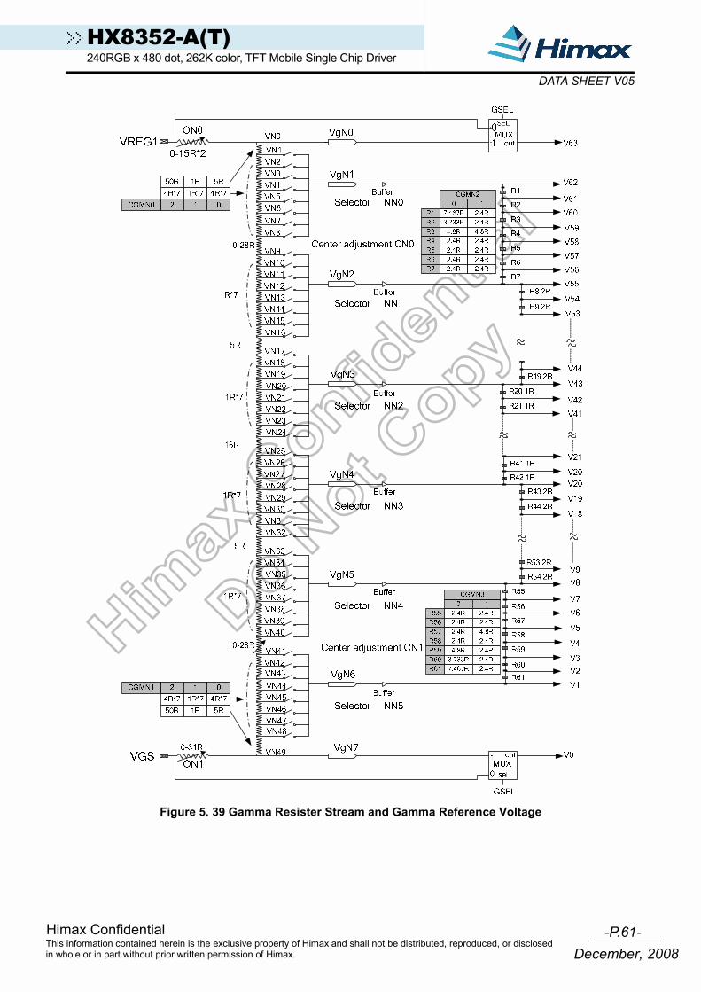
-P.61- Himax Confidential
December, 2008This information contained herein is the exclusive property of Himax and shall not be distributed, reproduced, or disclosed in whole or in part without prior written permission of Himax.
HX8352-A(T) 240RGB x 480 dot, 262K color, TFT Mobile Single Chip Driver
DATA SHEET V05
Figure 5. 39 Gamma Resister Stream and Gamma Reference Voltage

-P.62- Himax Confidential
December, 2008This information contained herein is the exclusive property of Himax and shall not be distributed, reproduced, or disclosed in whole or in part without prior written permission of Himax.
HX8352-A(T) 240RGB x 480 dot, 262K color, TFT Mobile Single Chip Driver
DATA SHEET V055.9.1.5 Variable resister
There are two types of variable resistors, one is for center adjustment, the other is for offset adjustment. The resistances are decided by setting values in the center adjustment, offset adjustment registers. Their relationship is shown as below.
Value in Register
O(P/N)0 3-0
Resistance VRO(P/N)0 Value in Register
O(P/N)1 4-0 ResistanceVRO(P/N)1
Value in Register C(P/N)0/1 2-0
ResistanceVRC(P/N)0/1
0000 0R 00000 0R 000 0R 0001 2R 00001 1R 001 4R 0010 4R 00010 2R 010 8R
011 12R • •
• •
• •
• • 100 16R
1101 26R 11101 29R 101 20R 1110 28R 11110 30R 110 24R 1111 30R 11111 31R 111 28R
Table 5. 12 Offset Adjustment 0 Table 5. 13 Offset Adjustment 1 Table 5. 14 Center Adjustment
8 to 1 Selector
The 8 to 1 selector has eight input voltages generated by gamma resister stream, and outputs one reference voltages selected from inputs for gamma reference voltage generation by setting value in macro adjustment register. There are six 8 to 1 selectors and the relationship is shown as below.
Value in Register Voltage Level
M(P/N) 2-0 Vg(P/N) 1 Vg(P/N) 2 Vg(P/N) 3 Vg(P/N) 4 Vg(P/N) 5 Vg(P/N) 6000 VP(N)1 VP(N)9 VP(N)17 VP(N)25 VP(N)33 VP(N)41 001 VP(N)2 VP(N)10 VP(N)18 VP(N)26 VP(N)34 VP(N)42 010 VP(N)3 VP(N)11 VP(N)19 VP(N)27 VP(N)35 VP(N)43 011 VP(N)4 VP(N)12 VP(N)20 VP(N)28 VP(N)36 VP(N)44 100 VP(N)5 VP(N)13 VP(N)21 VP(N)29 VP(N)37 VP(N)45 101 VP(N)6 VP(N)14 VP(N)22 VP(N)30 VP(N)38 VP(N)46 110 VP(N)7 VP(N)15 VP(N)23 VP(N)31 VP(N)39 VP(N)47 111 VP(N)8 VP(N)16 VP(N)24 VP(N)32 VP(N)40 VP(N)48
Table 5. 15 Output Voltage of 8 to 1 Selector
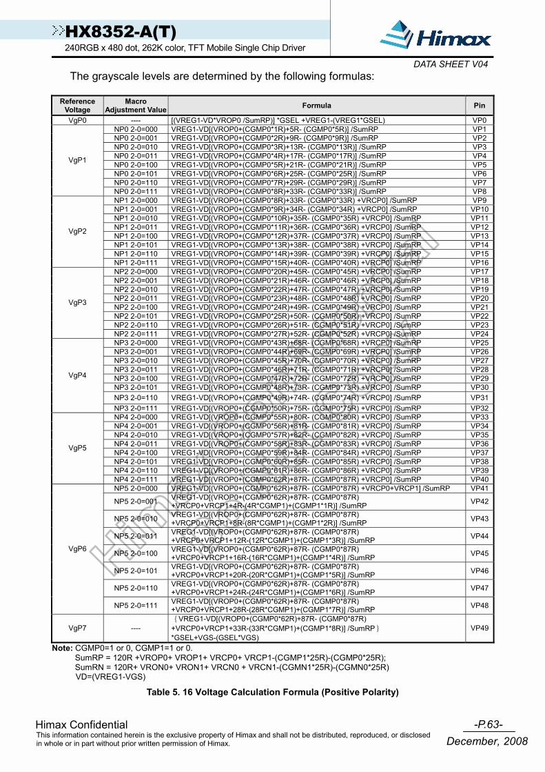
-P.63-
HX8352-A(T) 240RGB x 480 dot, 262K color, TFT Mobile Single Chip Driver DATA SHEET V04
Himax Confidential This information contained herein is the exclusive property of Himax and shall not be distributed, reproduced, or disclosed in whole or in part without prior written permission of Himax. December, 2008
The grayscale levels are determined by the following formulas:
Reference Voltage
Macro Adjustment Value Formula Pin
VgP0 ---- [(VREG1-VD*VROP0 /SumRP)] *GSEL +VREG1-(VREG1*GSEL) VP0NP0 2-0=000 VREG1-VD[(VROP0+(CGMP0*1R)+5R- (CGMP0*5R)] /SumRP VP1NP0 2-0=001 VREG1-VD[(VROP0+(CGMP0*2R)+9R- (CGMP0*9R)] /SumRP VP2NP0 2-0=010 VREG1-VD[(VROP0+(CGMP0*3R)+13R- (CGMP0*13R)] /SumRP VP3NP0 2-0=011 VREG1-VD[(VROP0+(CGMP0*4R)+17R- (CGMP0*17R)] /SumRP VP4NP0 2-0=100 VREG1-VD[(VROP0+(CGMP0*5R)+21R- (CGMP0*21R)] /SumRP VP5NP0 2-0=101 VREG1-VD[(VROP0+(CGMP0*6R)+25R- (CGMP0*25R)] /SumRP VP6NP0 2-0=110 VREG1-VD[(VROP0+(CGMP0*7R)+29R- (CGMP0*29R)] /SumRP VP7
VgP1
NP0 2-0=111 VREG1-VD[(VROP0+(CGMP0*8R)+33R- (CGMP0*33R)] /SumRP VP8NP1 2-0=000 VREG1-VD[(VROP0+(CGMP0*8R)+33R- (CGMP0*33R) +VRCP0] /SumRP VP9NP1 2-0=001 VREG1-VD[(VROP0+(CGMP0*9R)+34R- (CGMP0*34R) +VRCP0] /SumRP VP10NP1 2-0=010 VREG1-VD[(VROP0+(CGMP0*10R)+35R- (CGMP0*35R) +VRCP0] /SumRP VP11NP1 2-0=011 VREG1-VD[(VROP0+(CGMP0*11R)+36R- (CGMP0*36R) +VRCP0] /SumRP VP12NP1 2-0=100 VREG1-VD[(VROP0+(CGMP0*12R)+37R- (CGMP0*37R) +VRCP0] /SumRP VP13NP1 2-0=101 VREG1-VD[(VROP0+(CGMP0*13R)+38R- (CGMP0*38R) +VRCP0] /SumRP VP14NP1 2-0=110 VREG1-VD[(VROP0+(CGMP0*14R)+39R- (CGMP0*39R) +VRCP0] /SumRP VP15
VgP2
NP1 2-0=111 VREG1-VD[(VROP0+(CGMP0*15R)+40R- (CGMP0*40R) +VRCP0] /SumRP VP16NP2 2-0=000 VREG1-VD[(VROP0+(CGMP0*20R)+45R- (CGMP0*45R) +VRCP0] /SumRP VP17NP2 2-0=001 VREG1-VD[(VROP0+(CGMP0*21R)+46R- (CGMP0*46R) +VRCP0] /SumRP VP18NP2 2-0=010 VREG1-VD[(VROP0+(CGMP0*22R)+47R- (CGMP0*47R) +VRCP0] /SumRP VP19NP2 2-0=011 VREG1-VD[(VROP0+(CGMP0*23R)+48R- (CGMP0*48R) +VRCP0] /SumRP VP20NP2 2-0=100 VREG1-VD[(VROP0+(CGMP0*24R)+49R- (CGMP0*49R) +VRCP0] /SumRP VP21NP2 2-0=101 VREG1-VD[(VROP0+(CGMP0*25R)+50R- (CGMP0*50R) +VRCP0] /SumRP VP22NP2 2-0=110 VREG1-VD[(VROP0+(CGMP0*26R)+51R- (CGMP0*51R) +VRCP0] /SumRP VP23
VgP3
NP2 2-0=111 VREG1-VD[(VROP0+(CGMP0*27R)+52R- (CGMP0*52R) +VRCP0] /SumRP VP24NP3 2-0=000 VREG1-VD[(VROP0+(CGMP0*43R)+68R- (CGMP0*68R) +VRCP0] /SumRP VP25NP3 2-0=001 VREG1-VD[(VROP0+(CGMP0*44R)+69R- (CGMP0*69R) +VRCP0] /SumRP VP26NP3 2-0=010 VREG1-VD[(VROP0+(CGMP0*45R)+70R- (CGMP0*70R) +VRCP0] /SumRP VP27NP3 2-0=011 VREG1-VD[(VROP0+(CGMP0*46R)+71R- (CGMP0*71R) +VRCP0] /SumRP VP28NP3 2-0=100 VREG1-VD[(VROP0+(CGMP0*47R)+72R- (CGMP0*72R) +VRCP0] /SumRP VP29NP3 2-0=101 VREG1-VD[(VROP0+(CGMP0*48R)+73R- (CGMP0*73R) +VRCP0] /SumRP VP30NP3 2-0=110 VREG1-VD[(VROP0+(CGMP0*49R)+74R- (CGMP0*74R) +VRCP0] /SumRP VP31
VgP4
NP3 2-0=111 VREG1-VD[(VROP0+(CGMP0*50R)+75R- (CGMP0*75R) +VRCP0] /SumRP VP32NP4 2-0=000 VREG1-VD[(VROP0+(CGMP0*55R)+80R- (CGMP0*80R) +VRCP0] /SumRP VP33NP4 2-0=001 VREG1-VD[(VROP0+(CGMP0*56R)+81R- (CGMP0*81R) +VRCP0] /SumRP VP34NP4 2-0=010 VREG1-VD[(VROP0+(CGMP0*57R)+82R- (CGMP0*82R) +VRCP0] /SumRP VP35NP4 2-0=011 VREG1-VD[(VROP0+(CGMP0*58R)+83R- (CGMP0*83R) +VRCP0] /SumRP VP36NP4 2-0=100 VREG1-VD[(VROP0+(CGMP0*59R)+84R- (CGMP0*84R) +VRCP0] /SumRP VP37NP4 2-0=101 VREG1-VD[(VROP0+(CGMP0*60R)+85R- (CGMP0*85R) +VRCP0] /SumRP VP38NP4 2-0=110 VREG1-VD[(VROP0+(CGMP0*61R)+86R- (CGMP0*86R) +VRCP0] /SumRP VP39
VgP5
NP4 2-0=111 VREG1-VD[(VROP0+(CGMP0*62R)+87R- (CGMP0*87R) +VRCP0] /SumRP VP40NP5 2-0=000 VREG1-VD[(VROP0+(CGMP0*62R)+87R- (CGMP0*87R) +VRCP0+VRCP1] /SumRP VP41
NP5 2-0=001 VREG1-VD[(VROP0+(CGMP0*62R)+87R- (CGMP0*87R) +VRCP0+VRCP1+4R-(4R*CGMP1)+(CGMP1*1R)] /SumRP VP42
NP5 2-0=010 VREG1-VD[(VROP0+(CGMP0*62R)+87R- (CGMP0*87R) +VRCP0+VRCP1+8R-(8R*CGMP1)+(CGMP1*2R)] /SumRP VP43
NP5 2-0=011 VREG1-VD[(VROP0+(CGMP0*62R)+87R- (CGMP0*87R) +VRCP0+VRCP1+12R-(12R*CGMP1)+(CGMP1*3R)] /SumRP VP44
NP5 2-0=100 VREG1-VD[(VROP0+(CGMP0*62R)+87R- (CGMP0*87R) +VRCP0+VRCP1+16R-(16R*CGMP1)+(CGMP1*4R)] /SumRP VP45
NP5 2-0=101 VREG1-VD[(VROP0+(CGMP0*62R)+87R- (CGMP0*87R) +VRCP0+VRCP1+20R-(20R*CGMP1)+(CGMP1*5R)] /SumRP VP46
NP5 2-0=110 VREG1-VD[(VROP0+(CGMP0*62R)+87R- (CGMP0*87R) +VRCP0+VRCP1+24R-(24R*CGMP1)+(CGMP1*6R)] /SumRP VP47
VgP6
NP5 2-0=111 VREG1-VD[(VROP0+(CGMP0*62R)+87R- (CGMP0*87R) +VRCP0+VRCP1+28R-(28R*CGMP1)+(CGMP1*7R)] /SumRP VP48
VgP7 ---- {VREG1-VD[(VROP0+(CGMP0*62R)+87R- (CGMP0*87R) +VRCP0+VRCP1+33R-(33R*CGMP1)+(CGMP1*8R)] /SumRP}
*GSEL+VGS-(GSEL*VGS) VP49
Note: CGMP0=1 or 0, CGMP1=1 or 0. SumRP = 120R +VROP0+ VROP1+ VRCP0+ VRCP1-(CGMP1*25R)-(CGMP0*25R); SumRN = 120R+ VRON0+ VRON1+ VRCN0 + VRCN1-(CGMN1*25R)-(CGMN0*25R) VD=(VREG1-VGS)
Table 5. 16 Voltage Calculation Formula (Positive Polarity)

-P.64- Himax Confidential
December, 2008This information contained herein is the exclusive property of Himax and shall not be distributed, reproduced, or disclosed in whole or in part without prior written permission of Himax.
HX8352-A(T) 240RGB x 480 dot, 262K color, TFT Mobile Single Chip Driver
DATA SHEET V05
Grayscale Voltage Formula Grayscale
Voltage Formula
V0 VgP0 V32 VgP4+(VgP3-VgP4)*(11/23) V1 VgP1 V33 VgP4+(VgP3-VgP4)*(10/23)
V2 VgP2+(VgP1-VgP2)*(CGMP2*14.4/16.8)+ (VgP1-VgP2)*(1-CGMP2)*(18.133/25.6) V34 VgP4+(VgP3-VgP4)*(9/23)
V3 VgP2+(VgP1-VgP2)*(CGMP2*12/16.8)+ (VgP1-VgP2)*(1-CGMP2)*(4.4/25.6) V35 VgP4+(VgP3-VgP4)*(8/23)
V4 VgP2+(VgP1-VgP2)*(CGMP2*9.6/16.8)+ (VgP1-VgP2)*(1-CGMP2)*(9.6/25.6) V36 VgP4+(VgP3-VgP4)*(7/23)
V5 VgP2+(VgP1-VgP2)*(CGMP2*7.2/16.8)+ (VgP1-VgP2)*(1-CGMP2)*(7.2/25.6) V37 VgP4+(VgP3-VgP4)*(6/23)
V6 VgP2+(VgP1-VgP2)*(CGMP2*4.8/16.8)+ (VgP1-VgP2)*(1-CGMP2)*(4.8/25.6) V38 VgP4+(VgP3-VgP4)*(5/23)
V7 VgP2+(VgP1-VgP2)*(CGMP2*2.4/16.8)+ (VgP1-VgP2)*(1-CGMP2)*(2.4/25.6) V39 VgP4+(VgP3-VgP4)*(4/23)
V8 VgP2 V40 VgP4+(VgP3-VgP4)*(3/23) V9 VgP3+(VgP2-VgP3)*(22/24) V41 VgP4+(VgP3-VgP4)*(2/23)
V10 VgP3+(VgP2-VgP3)*(20/24) V42 VgP4+(VgP3-VgP4)*(1/23) V11 VgP3+(VgP2-VgP3)*(18/24) V43 VgP4 V12 VgP3+(VgP2-VgP3)*(16/24) V44 VgP5+(VgP4-VgP5)*(22/24) V13 VgP3+(VgP2-VgP3)*(14/24) V45 VgP5+(VgP4-VgP5)*(20/24) V14 VgP3+(VgP2-VgP3)*(12/24) V46 VgP5+(VgP4-VgP5)*(18/24) V15 VgP3+(VgP2-VgP3)*(10/24) V47 VgP5+(VgP4-VgP5)*(16/24) V16 VgP3+(VgP2-VgP3)*(8/24) V48 VgP5+(VgP4-VgP5)*(14/24) V17 VgP3+(VgP2-VgP3)*(6/24) V49 VgP5+(VgP4-VgP5)*(12/24) V18 VgP3+(VgP2-VgP3)*(4/24) V50 VgP5+(VgP4-VgP5)*(10/24) V19 VgP3+(VgP2-VgP3)*(2/24) V51 VgP5+(VgP4-VgP5)*(8/24) V20 VgP3 V52 VgP5+(VgP4-VgP5)*(6/24) V21 VgP4+(VgP3-VgP4)*(22/23) V53 VgP5+(VgP4-VgP5)*(4/24) V22 VgP4+(VgP3-VgP4)*(21/23) V54 VgP5+(VgP4-VgP5)*(2/24) V23 VgP4+(VgP3-VgP4)*(20/23) V55 VgP5
V24 VgP4+(VgP3-VgP4)*(19/23) V56 VgP6+(VgP5-VgP6)*(CGMP3*14.4/16.8)+ (VgP5-VgP6)*(1-CGMP3)*(23.2/25.6)
V25 VgP4+(VgP3-VgP4)*(18/23) V57 VgP6+(VgP5-VgP6)*(CGMP3*12/16.8)+ (VgP5-VgP6)*(1-CGMP3)*(20.8/25.6)
V26 VgP4+(VgP3-VgP4)*(17/23) V58 VgP6+(VgP5-VgP6)*(CGMP3*9.6/16.8)+ (VgP5-VgP6)*(1-CGMP3)*(18.4/25.6)
V27 VgP4+(VgP3-VgP4)*(16/23) V59 VgP6+(VgP5-VgP6)*(CGMP3*7.2/16.8)+ (VgP5-VgP6)*(1-CGMP3)*(16/25.6)
V28 VgP4+(VgP3-VgP4)*(15/23) V60 VgP6+(VgP5-VgP6)*(CGMP3*4.8/16.8)+ (VgP5-VgP6)*(1-CGMP3)*(11.2/25.6)
V29 VgP4+(VgP3-VgP4)*(14/23) V61 VgP6+(VgP5-VgP6)*(CGMP3*2.4/16.8)+ (VgP5-VgP6)*(1-CGMP3)*(7.467/25.6)
V30 VgP4+(VgP3-VgP4)*(13/23) V62 VgP6 V31 VgP4+(VgP3-VgP4)*(12/23) V63 VgP7
Table 5. 17 Voltage Calculation Formula of Grayscale Voltage (Positive Polarity)
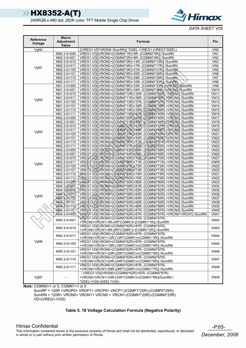
-P.65- Himax Confidential
December, 2008This information contained herein is the exclusive property of Himax and shall not be distributed, reproduced, or disclosed in whole or in part without prior written permission of Himax.
HX8352-A(T) 240RGB x 480 dot, 262K color, TFT Mobile Single Chip Driver
DATA SHEET V05
Reference Voltage
Macro Adjustment
Value Formula Pin
VgN0 - [(VREG1-VD*VRON0 /SumRN)] *GSEL +VREG1-(VREG1*GSEL) VN0 NN0 2-0=000 VREG1-VD[(VRON0+(CGMN0*1R)+5R- (CGMN0*5R)] /SumRN VN1 NN0 2-0=001 VREG1-VD[(VRON0+(CGMN0*2R)+9R- (CGMN0*9R)] /SumRN VN2 NN0 2-0=010 VREG1-VD[(VRON0+(CGMN0*3R)+13R- (CGMN0*13R)] /SumRN VN3 NN0 2-0=011 VREG1-VD[(VRON0+(CGMN0*4R)+17R- (CGMN0*17R)] /SumRN VN4 NN0 2-0=100 VREG1-VD[(VRON0+(CGMN0*5R)+21R- (CGMN0*21R)] /SumRN VN5 NN0 2-0=101 VREG1-VD[(VRON0+(CGMN0*6R)+25R- (CGMN0*25R)] /SumRN VN6 NN0 2-0=110 VREG1-VD[(VRON0+(CGMN0*7R)+29R- (CGMN0*29R)] /SumRN VN7
VgN1
NN0 2-0=111 VREG1-VD[(VRON0+(CGMN0*8R)+33R- (CGMN0*33R)] /SumRN VN8 NN1 2-0=000 VREG1-VD[(VRON0+(CGMN0*8R)+33R- (CGMN0*33R) +VRCN0] /SumRN VN9 NN1 2-0=001 VREG1-VD[(VRON0+(CGMN0*9R)+34R- (CGMN0*34R) +VRCN0] /SumRN VN10NN1 2-0=010 VREG1-VD[(VRON0+(CGMN0*10R)+35R- (CGMN0*35R) +VRCN0] /SumRN VN11NN1 2-0=011 VREG1-VD[(VRON0+(CGMN0*11R)+36R- (CGMN0*36R) +VRCN0] /SumRN VN12NN1 2-0=100 VREG1-VD[(VRON0+(CGMN0*12R)+37R- (CGMN0*37R) +VRCN0] /SumRN VN13NN1 2-0=101 VREG1-VD[(VRON0+(CGMN0*13R)+38R- (CGMN0*38R) +VRCN0] /SumRN VN14NN1 2-0=110 VREG1-VD[(VRON0+(CGMN0*14R)+39R- (CGMN0*39R) +VRCN0] /SumRN VN15
VgN2
NN1 2-0=111 VREG1-VD[(VRON0+(CGMN0*15R)+40R- (CGMN0*40R) +VRCN0] /SumRN VN16NN2 2-0=000 VREG1-VD[(VRON0+(CGMN0*20R)+45R- (CGMN0*45R) +VRCN0] /SumRN VN17NN2 2-0=001 VREG1-VD[(VRON0+(CGMN0*21R)+46R- (CGMN0*46R) +VRCN0] /SumRN VN18NN2 2-0=010 VREG1-VD[(VRON0+(CGMN0*22R)+47R- (CGMN0*47R) +VRCN0] /SumRN VN19NN2 2-0=011 VREG1-VD[(VRON0+(CGMN0*23R)+48R- (CGMN0*48R) +VRCN0] /SumRN VN20NN2 2-0=100 VREG1-VD[(VRON0+(CGMN0*24R)+49R- (CGMN0*49R) +VRCN0] /SumRN VN21NN2 2-0=101 VREG1-VD[(VRON0+(CGMN0*25R)+50R- (CGMN0*50R) +VRCN0] /SumRN VN22NN2 2-0=110 VREG1-VD[(VRON0+(CGMN0*26R)+51R- (CGMN0*51R) +VRCN0] /SumRN VN23
VgN3
NN2 2-0=111 VREG1-VD[(VRON0+(CGMN0*27R)+52R- (CGMN0*52R) +VRCN0] /SumRN VN24NN3 2-0=000 VREG1-VD[(VRON0+(CGMN0*43R)+68R- (CGMN0*68R) +VRCN0] /SumRN VN25NN3 2-0=001 VREG1-VD[(VRON0+(CGMN0*44R)+69R- (CGMN0*69R) +VRCN0] /SumRN VN26NN3 2-0=010 VREG1-VD[(VRON0+(CGMN0*45R)+70R- (CGMN0*70R) +VRCN0] /SumRN VN27NN3 2-0=011 VREG1-VD[(VRON0+(CGMN0*46R)+71R- (CGMN0*71R) +VRCN0] /SumRN VNP8NN3 2-0=100 VREG1-VD[(VRON0+(CGMN0*47R)+72R- (CGMN0*72R) +VRCN0] /SumRN VN29NN3 2-0=101 VREG1-VD[(VRON0+(CGMN0*48R)+73R- (CGMN0*73R) +VRCN0] /SumRN VN30NN3 2-0=110 VREG1-VD[(VRON0+(CGMN0*49R)+74R- (CGMN0*74R) +VRCN0] /SumRN VN31
VgN4
NN3 2-0=111 VREG1-VD[(VRON0+(CGMN0*50R)+75R- (CGMN0*75R) +VRCN0] /SumRN VN32NN4 2-0=000 VREG1-VD[(VRON0+(CGMN0*55R)+80R- (CGMN0*80R) +VRCN0] /SumRN VN33NN4 2-0=001 VREG1-VD[(VRON0+(CGMN0*56R)+81R- (CGMN0*81R) +VRCN0] /SumRN VN34NN4 2-0=010 VREG1-VD[(VRON0+(CGMN0*57R)+82R- (CGMN0*82R) +VRCN0] /SumRN VN35NN4 2-0=011 VREG1-VD[(VRON0+(CGMN0*58R)+83R- (CGMN0*83R) +VRCN0] /SumRN VN36NN4 2-0=100 VREG1-VD[(VRON0+(CGMN0*59R)+84R- (CGMN0*84R) +VRCN0] /SumRN VN37NN4 2-0=101 VREG1-VD[(VRON0+(CGMN0*60R)+85R- (CGMN0*85R) +VRCN0] /SumRN VN38NN4 2-0=110 VREG1-VD[(VRON0+(CGMN0*61R)+86R- (CGMN0*86R) +VRCN0] /SumRN VN39
VgN5
NN4 2-0=111 VREG1-VD[(VRON0+(CGMN0*62R)+87R- (CGMN0*87R) +VRCN0] /SumRN VN40NN5 2-0=000 VREG1-VD[(VRON0+(CGMN0*62R)+87R- (CGMN0*87R) +VRCN0+VRCN1] /SumRN VN41
NN5 2-0=001 VREG1-VD[(VRON0+(CGMN0*62R)+87R- (CGMN0*87R) +VRCN0+VRCN1+4R-(4R*CGMN1)+(CGMN1*1R)] /SumRN VN42
NN5 2-0=010 VREG1-VD[(VRON0+(CGMN0*62R)+87R- (CGMN0*87R) +VRCN0+VRCN1+8R-(8R*CGMN1)+(CGMN1*2R)] /SumRN VN43
NN5 2-0=011 VREG1-VD[(VRON0+(CGMN0*62R)+87R- (CGMN0*87R) +VRCN0+VRCN1+12R-(12R*CGMN1)+(CGMN1*3R)] /SumRN VN44
NN5 2-0=100 VREG1-VD[(VRON0+(CGMN0*62R)+87R- (CGMN0*87R) +VRCN0+VRCN1+16R-(16R*CGMN1)+(CGMN1*4R)] /SumRN VN45
NN5 2-0=101 VREG1-VD[(VRON0+(CGMN0*62R)+87R- (CGMN0*87R) +VRCN0+VRCN1+20R-(20R*CGMN1)+(CGMN1*5R)] /SumRN VN46
NN5 2-0=110 VREG1-VD[(VRON0+(CGMN0*62R)+87R- (CGMN0*87R) +VRCN0+VRCN1+24R-(24R*CGMN1)+(CGMN1*6R)] /SumRN VN47
VgN6
NN5 2-0=111 VREG1-VD[(VRON0+(CGMN0*62R)+87R- (CGMN0*87R) +VRCN0+VRCN1+28R-(28R*CGMN1)+(CGMN1*7R)] /SumRN VN48
VgN7 - {VREG1-VD[(VRON0+(CGMN0*62R)+87R- (CGMN0*87R) +VRCN0+VRCN1+33R-(33R*CGMN1)+(CGMN1*8R)]/SumRN}
*GSEL+VGS-(GSEL*VGS) VN49
Note: CGMN0=1 or 0, CGMN1=1 or 0 SumRP = 120R +VROP0+ VROP1+ VRCP0+ VRCP1-(CGMP1*25R)-(CGMP0*25R); SumRN = 120R+ VRON0+ VRON1+ VRCN0 + VRCN1-(CGMN1*25R)-(CGMN0*25R) VD=(VREG1-VGS)
Table 5. 18 Voltage Calculation Formula (Negative Polarity)

-P.66- Himax Confidential
December, 2008This information contained herein is the exclusive property of Himax and shall not be distributed, reproduced, or disclosed in whole or in part without prior written permission of Himax.
HX8352-A(T) 240RGB x 480 dot, 262K color, TFT Mobile Single Chip Driver
DATA SHEET V05
Grayscale
Voltage Formula Grayscale Voltage Formula
V63 VgN0 V31 VgN4+(VgN3-VgN4)*(11/23) V62 VgN1 V30 VgN4+(VgN3-VgN4)*(10/23)
V61 VgN2+(VgN1-VgN2)*(CGMN2*14.4/16.8)+ (VgN1-VgN2)*(1-CGMN2)*(18.133/25.6)
V29 VgN4+(VgN3-VgN4)*(9/23)
V60 VgN2+(VgN1-VgN2)*(CGMN2*12/16.8)+ (VgN1-VgN2)*(1-CGMN2)*(14.4/25.6)
V28 VgN4+(VgN3-VgN4)*(8/23)
V59 VgN2+(VgN1-VgN2)*(CGMN2*9.6/16.8)+ (VgN1-VgN2)*(1-CGMN2)*(9.6/25.6)
V27 VgN4+(VgN3-VgN4)*(7/23)
V58 VgN2+(VgN1-VgN2)*(CGMN2*7.2/16.8)+ (VgN1-VgN2)*(1-CGMN2)*(7.2/25.6)
V26 VgN4+(VgN3-VgN4)*(6/23)
V57 VgN2+(VgN1-VgN2)*(CGMN2*4.8/16.8)+ (VgN1-VgN2)*(1-CGMN2)*(4.8/25.6)
V25 VgN4+(VgN3-VgN4)*(5/23)
V56 VgN2+(VgN1-VgN2)*(CGMN2*2.4/16.8)+ (VgN1-VgN2)*(1-CGMN2)*(2.4/25.6)
V24 VgN4+(VgN3-VgN4)*(4/23)
V55 VgN2 V23 VgN4+(VgN3-VgN4)*(3/23) V54 VgN3+(VgN2-VgN3)*(22/24) V22 VgN4+(VgN3-VgN4)*(2/23) V53 VgN3+(VgN2-VgN3)*(20/24) V21 VgN4+(VgN3-VgN4)*(1/23) V52 VgN3+(VgN2-VgN3)*(18/24) V20 VgN4 V51 VgN3+(VgN2-VgN3)*(16/24) V19 VgN5+(VgN4-VgN5)*(22/24) V50 VgN3+(VgN2-VgN3)*(14/24) V18 VgN5+(VgN4-VgN5)*(20/24) V49 VgN3+(VgN2-VgN3)*(12/24) V17 VgN5+(VgN4-VgN5)*(18/24) V48 VgN3+(VgN2-VgN3)*(10/24) V16 VgN5+(VgN4-VgN5)*(16/24) V47 VgN3+(VgN2-VgN3)*(8/24) V15 VgN5+(VgN4-VgN5)*(14/24) V46 VgN3+(VgN2-VgN3)*(6/24) V14 VgN5+(VgN4-VgN5)*(12/24) V45 VgN3+(VgN2-VgN3)*(4/24) V13 VgN5+(VgN4-VgN5)*(10/24) V44 VgN3+(VgN2-VgN3)*(2/24) V12 VgN5+(VgN4-VgN5)*(8/24) V43 VgN3 V11 VgN5+(VgN4-VgN5)*(6/24) V42 VgN4+(VgN3-VgN4)*(22/23) V10 VgN5+(VgN4-VgN5)*(4/24) V41 VgN4+(VgN3-VgN4)*(21/23) V9 VgN5+(VgN4-VgN5)*(2/24) V40 VgN4+(VgN3-VgN4)*(20/23) V8 VgN5 V39 VgN4+(VgN3-VgN4)*(19/23) V7 VgN6+(VgN5-VgN6)*(CGMN3*14.4/16.8)+
(VgN5-VgN6)*(1-CGMN3)*(23.2/25.6) V38 VgN4+(VgN3-VgN4)*(18/23) V6 VgN6+(VgN5-VgN6)*(CGMN3*12/16.8)+
(VgN5-VgN6)*(1-CGMN3)*(20.8/25.6) V37 VgN4+(VgN3-VgN4)*(17/23) 5 VgN6+(VgN5-VgN6)*(CGMN3*9.6/16.8)+
(VgN5-VgN6)*(1-CGMN3)*(18.4/25.6) V36 VgN4+(VgN3-VgN4)*(16/23) V4 VgN6+(VgN5-VgN6)*(CGMN3*7.2/16.8)+
(VgN5-VgN6)*(1-CGMN3)*(16/25.6) V35 VgN4+(VgN3-VgN4)*(15/23) V3 VgN6+(VgN5-VgN6)*(CGMN3*4.8/16.8)+
(VgN5-VgN6)*(1-CGMN3)*(11.2/25.6) V34 VgN4+(VgN3-VgN4)*(14/23) V2 VgN6+(VgN5-VgN6)*(CGMN3*2.4/16.8)+
(VgN5-VgN6)*(1-CGMN3)*(7.467/25.6) V33 VgN4+(VgN3-VgN4)*(13/23) V1 VgN6 V32 VgN4+(VgN3-VgN4)*(12/23) V0 VgN7
Table 5. 19 Voltage Calculation Formula of Grayscale Voltage (Negative Polarity)
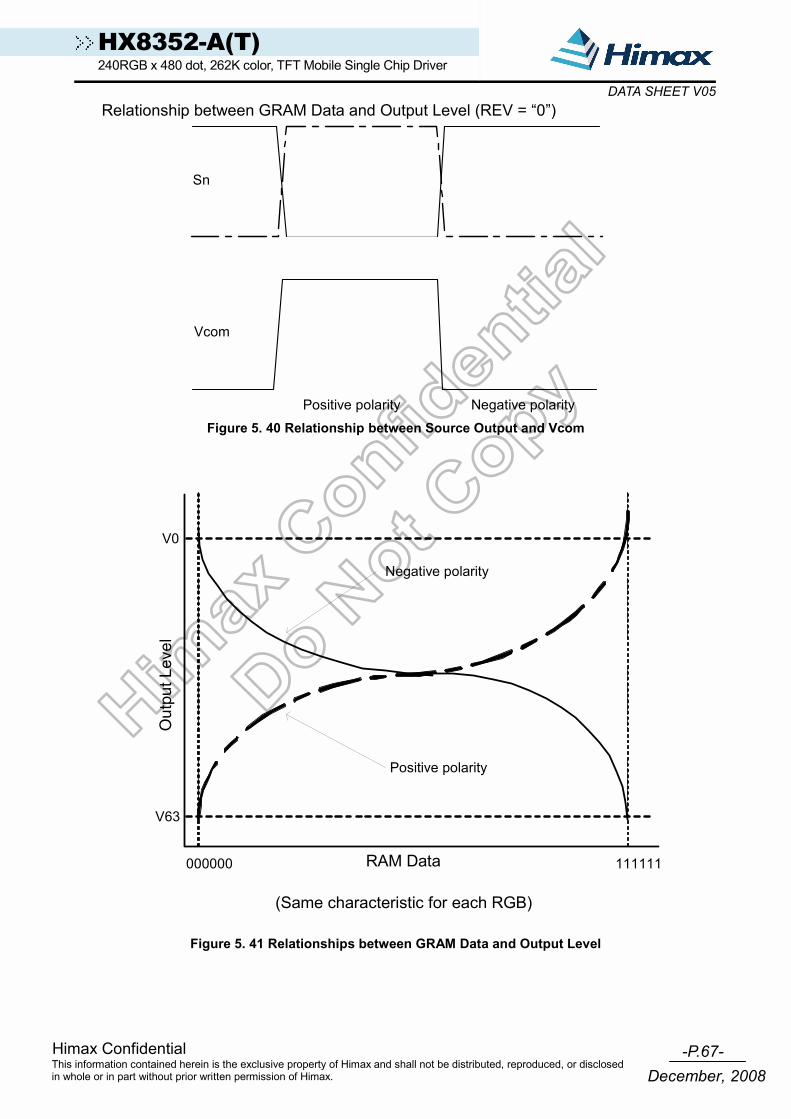
-P.67- Himax Confidential
December, 2008This information contained herein is the exclusive property of Himax and shall not be distributed, reproduced, or disclosed in whole or in part without prior written permission of Himax.
HX8352-A(T) 240RGB x 480 dot, 262K color, TFT Mobile Single Chip Driver
DATA SHEET V05Relationship between GRAM Data and Output Level (REV = “0”)
Positive polarity Negative polarity
Sn
Vcom
Figure 5. 40 Relationship between Source Output and Vcom
Negative polarity
Positive polarity
000000 111111RAM Data
(Same characteristic for each RGB)
V63
V0
Out
put L
evel
Figure 5. 41 Relationships between GRAM Data and Output Level
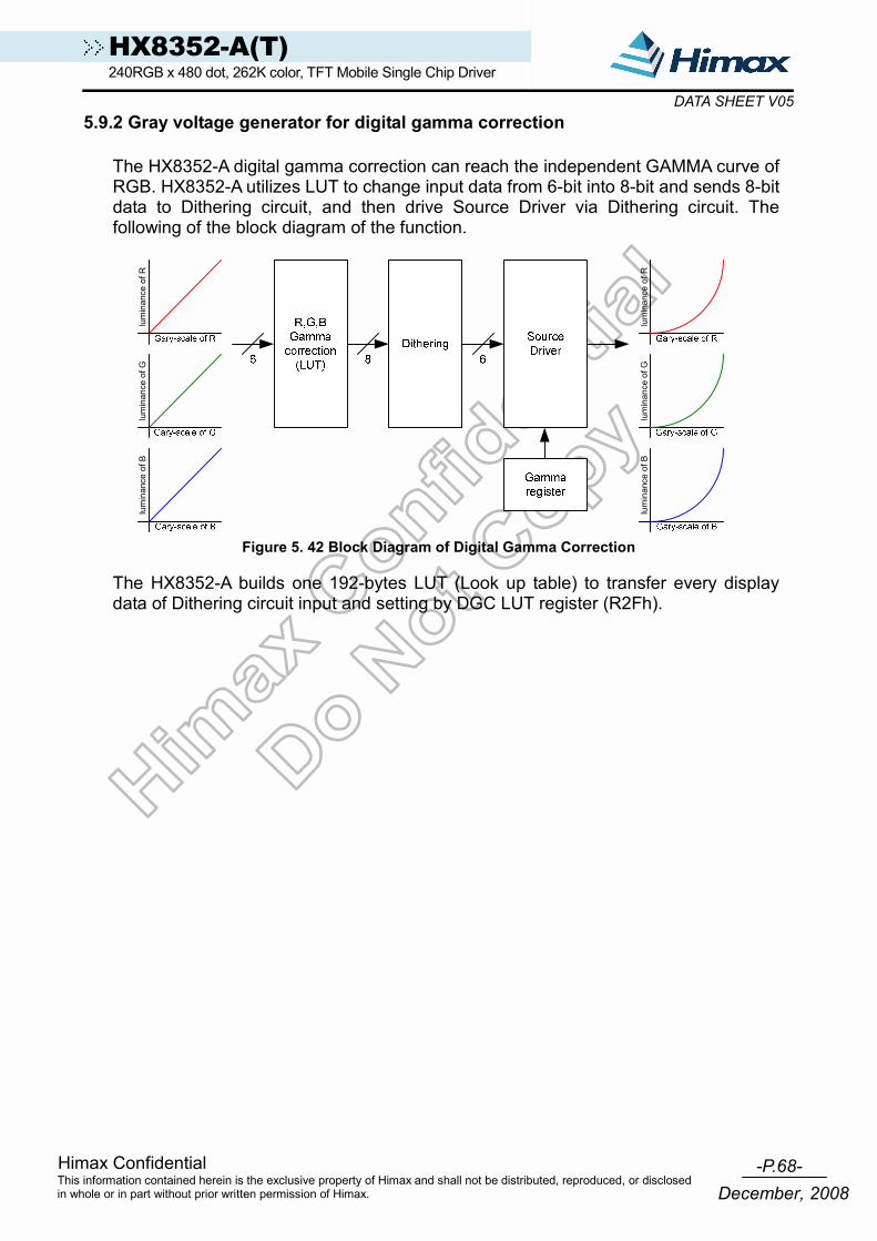
-P.68- Himax Confidential
December, 2008This information contained herein is the exclusive property of Himax and shall not be distributed, reproduced, or disclosed in whole or in part without prior written permission of Himax.
HX8352-A(T) 240RGB x 480 dot, 262K color, TFT Mobile Single Chip Driver
DATA SHEET V055.9.2 Gray voltage generator for digital gamma correction
The HX8352-A digital gamma correction can reach the independent GAMMA curve of RGB. HX8352-A utilizes LUT to change input data from 6-bit into 8-bit and sends 8-bit data to Dithering circuit, and then drive Source Driver via Dithering circuit. The following of the block diagram of the function.
lum
inan
ce o
f Rlu
min
ance
of G
lum
inan
ce o
f B
lum
inan
ce o
f Rlu
min
ance
of G
lum
inan
ce o
f B
Figure 5. 42 Block Diagram of Digital Gamma Correction
The HX8352-A builds one 192-bytes LUT (Look up table) to transfer every display data of Dithering circuit input and setting by DGC LUT register (R2Fh).
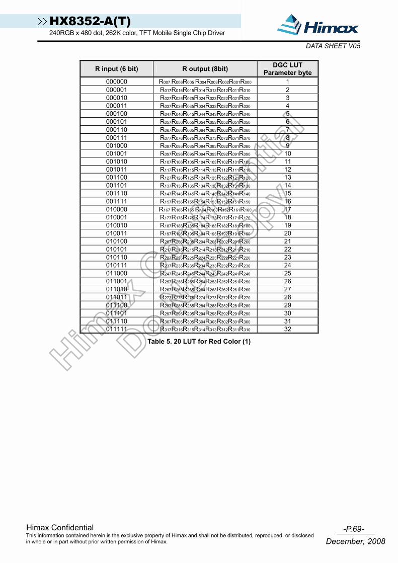
-P.69- Himax Confidential
December, 2008This information contained herein is the exclusive property of Himax and shall not be distributed, reproduced, or disclosed in whole or in part without prior written permission of Himax.
HX8352-A(T) 240RGB x 480 dot, 262K color, TFT Mobile Single Chip Driver
DATA SHEET V05
R input (6 bit) R output (8bit) DGC LUT Parameter byte
000000 R007 R006R005 R004R003R002R001R000 1 000001 R017R016R015R014R013R012R011R010 2 000010 R027R026R025R024R023R022R021R020 3 000011 R037R036R035R034R033R032R031R030 4 000100 R047R046R045R044R043R042R041R040 5 000101 R057R056R055R054R053R052R051R050 6 000110 R067R066R065R064R063R062R061R060 7 000111 R077R076R075R074R073R072R071R070 8 001000 R087R086R085R084R083R082R081R080 9 001001 R097R096R095R094R093R092R091R090 10 001010 R107R106R105R104R103R102R101R100 11 001011 R117R116R115R114R113R112R111R110 12 001100 R127R126R125R124R123R122R121R120 13 001101 R137R136R135R134R133R132R131R130 14 001110 R147R146R145R144R143R142R141R140 15 001111 R157R156R155R154R153R152R151R150 16 010000 R167 R166R165 R164R163R162R161R160 17 010001 R177R176R175R174R173R172R171R170 18 010010 R187R186R185R184R183R182R181R180 19 010011 R197R196R195R194R193R192R191R190 20 010100 R207R206R205R204R203R202R201R200 21 010101 R217R216R215R214R213R212R211R210 22 010110 R227R226R225R224R223R222R221R220 23 010111 R237R236R235R234R233R232R231R230 24 011000 R247R246R245R244R243R242R241R240 25 011001 R257R256R255R254R253R252R251R250 26 011010 R267R266R265R264R263R262R261R260 27 011011 R277R276R275R274R273R272R271R270 28 011100 R287R286R285R284R283R282R281R280 29 011101 R297R296R295R294R293R292R291R290 30 011110 R307R306R305R304R303R302R301R300 31 011111 R317R316R315R314R313R312R311R310 32
Table 5. 20 LUT for Red Color (1)

-P.70- Himax Confidential
December, 2008This information contained herein is the exclusive property of Himax and shall not be distributed, reproduced, or disclosed in whole or in part without prior written permission of Himax.
HX8352-A(T) 240RGB x 480 dot, 262K color, TFT Mobile Single Chip Driver
DATA SHEET V05
R input (6 bit) R output (8bit) DGC LUT Parameter byte
100000 R327 R326R325 R324R323R322R321R320 33 100001 R337R336R335R334R333R332R331R330 34 100010 R347R346R345R344R343R342R341R340 35 100011 R357R356R355R354R353R352R351R350 36 100100 R367R366R365R364R363R362R361R360 37 100101 R377R376R375R374R373R372R371R370 38 100110 R387R386R385R384R383R382R381R380 39 100111 R397R396R395R394R393R392R391R390 40 101000 R407R406R405R404R403R402R401R400 41 101001 R417R416R415R414R413R412R411R410 42 101010 R427R426R425R424R423R422R421R420 43 101011 R437R436R435R434R433R432R431R430 44 101100 R447R446R445R444R443R442R441R440 45 101101 R457R456R455R454R453R452R451R450 46 101110 R467R466R465R464R463R462R461R460 47 101111 R477R476R475R474R473R472R471R470 48 110000 R487 R486R485 R484R483R482R481R480 49 110001 R497R496R495R494R493R492R491R490 50 110010 R507R506R505R504R503R502R501R500 51 110011 R517R516R515R514R513R512R511R510 52 110100 R527R526R525R524R523R522R521R520 53 110101 R537R536R535R534R533R532R531R530 54 110110 R547R546R545R544R543R542R541R540 55 110111 R557R556R555R554R553R552R551R550 56 111000 R567R566R565R564R563R562R561R560 57 111001 R577R576R575R574R573R572R571R570 58 111010 R587R586R585R584R583R582R581R580 59 111011 R597R596R595R594R593R592R591R590 60 111100 R607R606R605R604R603R602R601R600 61 111101 R617R616R615R614R613R612R611R610 62 111110 R627R626R625R624R623R622R621R620 63 111111 R637R636R635R634R633R632R631R630 64
Table 5. 21 LUT for Red Color (2)

-P.71- Himax Confidential
December, 2008This information contained herein is the exclusive property of Himax and shall not be distributed, reproduced, or disclosed in whole or in part without prior written permission of Himax.
HX8352-A(T) 240RGB x 480 dot, 262K color, TFT Mobile Single Chip Driver
DATA SHEET V05
G input (6 bit) G output (8bit) DGC LUT Parameter byte
000000 G007 G006G005 G004G003G002G001G000 65 000001 G017G016G015G014G013G012G011G010 66 000010 G027G026G025G024G023G022G021G020 67 000011 G037G036G035G034G033G032G031G030 68 000100 G047G046G045G044G043G042G041G040 69 000101 G057G056G055G054G053G052G051G050 70 000110 G067G066G065G064G063G062G061G060 71 000111 G077G076G075G074G073G072G071G070 72 001000 G087G086G085G084G083G082G081G080 73 001001 G097G096G095G094G093G092G091G090 74 001010 G107G106G105G104G103G102G101G100 75 001011 G117G116G115G114G113G112G111G110 76 001100 G127G126G125G124G123G122G121G120 77 001101 G137G136G135G134G133G132G131G130 78 001110 G147G146G145G144G143G142G141G140 79 001111 G157G156G155G154G153G152G151G150 80 010000 G167 G166G165 G164G163G162G161G160 81 010001 G177G176G175G174G173G172G171G170 82 010010 G187G186G185G184G183G182G181G180 83 010011 G197G196G195G194G193G192G191G190 84 010100 G207G206G205G204G203G202G201G200 85 010101 G217G216G215G214G213G212G211G210 86 010110 G227G226G225G224G223G222G221G220 87 010111 G237G236G235G234G233G232G231G230 88 011000 G247G246G245G244G243G242G241G240 89 011001 G257G256G255G254G253G252G251G250 90 011010 G267G266G265G264G263G262G261G260 91 011011 G277G276G275G274G273G272G271G270 92 011100 G287G286G285G284G283G282G281G280 93 011101 G297G296G295G294G293G292G291G290 94 011110 G307G306G305G304G303G302G301G300 95 011111 G317G316G315G314G313G312G311G310 96
Table 5. 22 LUT for Green Color (1)
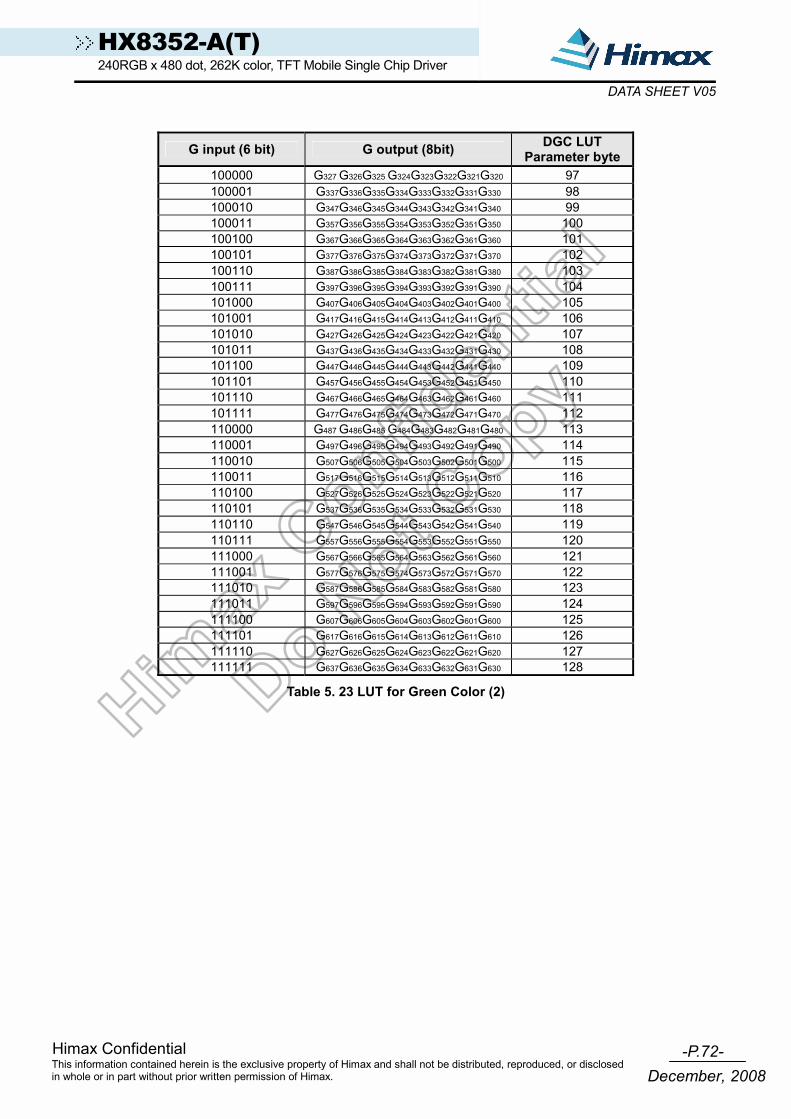
-P.72- Himax Confidential
December, 2008This information contained herein is the exclusive property of Himax and shall not be distributed, reproduced, or disclosed in whole or in part without prior written permission of Himax.
HX8352-A(T) 240RGB x 480 dot, 262K color, TFT Mobile Single Chip Driver
DATA SHEET V05
G input (6 bit) G output (8bit) DGC LUT Parameter byte
100000 G327 G326G325 G324G323G322G321G320 97 100001 G337G336G335G334G333G332G331G330 98 100010 G347G346G345G344G343G342G341G340 99 100011 G357G356G355G354G353G352G351G350 100 100100 G367G366G365G364G363G362G361G360 101 100101 G377G376G375G374G373G372G371G370 102 100110 G387G386G385G384G383G382G381G380 103 100111 G397G396G395G394G393G392G391G390 104 101000 G407G406G405G404G403G402G401G400 105 101001 G417G416G415G414G413G412G411G410 106 101010 G427G426G425G424G423G422G421G420 107 101011 G437G436G435G434G433G432G431G430 108 101100 G447G446G445G444G443G442G441G440 109 101101 G457G456G455G454G453G452G451G450 110 101110 G467G466G465G464G463G462G461G460 111 101111 G477G476G475G474G473G472G471G470 112 110000 G487 G486G485 G484G483G482G481G480 113 110001 G497G496G495G494G493G492G491G490 114 110010 G507G506G505G504G503G502G501G500 115 110011 G517G516G515G514G513G512G511G510 116 110100 G527G526G525G524G523G522G521G520 117 110101 G537G536G535G534G533G532G531G530 118 110110 G547G546G545G544G543G542G541G540 119 110111 G557G556G555G554G553G552G551G550 120 111000 G567G566G565G564G563G562G561G560 121 111001 G577G576G575G574G573G572G571G570 122 111010 G587G586G585G584G583G582G581G580 123 111011 G597G596G595G594G593G592G591G590 124 111100 G607G606G605G604G603G602G601G600 125 111101 G617G616G615G614G613G612G611G610 126 111110 G627G626G625G624G623G622G621G620 127 111111 G637G636G635G634G633G632G631G630 128
Table 5. 23 LUT for Green Color (2)

-P.73- Himax Confidential
December, 2008This information contained herein is the exclusive property of Himax and shall not be distributed, reproduced, or disclosed in whole or in part without prior written permission of Himax.
HX8352-A(T) 240RGB x 480 dot, 262K color, TFT Mobile Single Chip Driver
DATA SHEET V05
B input (6 bit) B output (8bit) DGC LUT Parameter byte
000000 B007 B006B005 B004B003B002B001B000 129 000001 B017B016B015B014B013B012B011B010 130 000010 B027B026B025B024B023B022B021B020 131 000011 B037B036B035B034B033B032B031B030 132 000100 B047B046B045B044B043B042B041B040 133 000101 B057B056B055B054B053B052B051B050 134 000110 B067B066B065B064B063B062B061B060 135 000111 B077B076B075B074B073B072B071B070 136 001000 B087B086B085B084B083B082B081B080 137 001001 B097B096B095B094B093B092B091B090 138 001010 B107B106B105B104B103B102B101B100 139 001011 B117B116B115B114B113B112B111B110 140 001100 B127B126B125B124B123B122B121B120 141 001101 B137B136B135B134B133B132B131B130 142 001110 B147B146B145B144B143B142B141B140 143 001111 B157B156B155B154B153B152B151B150 144 010000 B167 B166B165 B164B163B162B161B160 145 010001 B177B176B175B174B173B172B171B170 146 010010 B187B186B185B184B183B182B181B180 147 010011 B197B196B195B194B193B192B191B190 148 010100 B207B206B205B204B203B202B201B200 149 010101 B217B216B215B214B213B212B211B210 150 010110 B227B226B225B224B223B222B221B220 151 010111 B237B236B235B234B233B232B231B230 152 011000 B247B246B245B244B243B242B241B240 153 011001 B257B256B255B254B253B252B251B250 154 011010 B267B266B265B264B263B262B261B260 155 011011 B277B276B275B274B273B272B271B270 156 011100 B287B286B285B284B283B282B281B280 157 011101 B297B296B295B294B293B292B291B290 158 011110 B307B306B305B304B303B302B301B300 159 011111 B317B316B315B314B313B312B311B310 160
Table 5. 24 LUT for Blue Color (1)

-P.74- Himax Confidential
December, 2008This information contained herein is the exclusive property of Himax and shall not be distributed, reproduced, or disclosed in whole or in part without prior written permission of Himax.
HX8352-A(T) 240RGB x 480 dot, 262K color, TFT Mobile Single Chip Driver
DATA SHEET V05
B input (6 bit) B output (8bit) DGC LUT Parameter byte
100000 B327 B326B325 B324B323B322B321B320 161 100001 B337B336B335B334B333B332B331B330 162 100010 B347B346B345B344B343B342B341B340 163 100011 B357B356B355B354B353B352B351B350 164 100100 B367B366B365B364B363B362B361B360 165 100101 B377B376B375B374B373B372B371B370 166 100110 B387B386B385B384B383B382B381B380 167 100111 B397B396B395B394B393B392B391B390 168 101000 B407B406B405B404B403B402B401B400 169 101001 B417B416B415B414B413B412B411B410 170 101010 B427B426B425B424B423B422B421B420 171 101011 B437B436B435B434B433B432B431B430 172 101100 B447B446B445B444B443B442B441B440 173 101101 B457B456B455B454B453B452B451B450 174 101110 B467B466B465B464B463B462B461B460 175 101111 B477B476B475B474B473B472B471B470 176 110000 B487 B486B485 B484B483B482B481B480 177 110001 B497B496B495B494B493B492B491B490 178 110010 B507B506B505B504B503B502B501B500 179 110011 B517B516B515B514B513B512B511B510 180 110100 B527B526B525B524B523B522B521B520 181 110101 B537B536B535B534B533B532B531B530 182 110110 B547B546B545B544B543B542B541B540 183 110111 B557B556B555B554B553B552B551B550 184 111000 B567B566B565B564B563B562B561B560 185 111001 B577B576B575B574B573B572B571B570 186 111010 B587B586B585B584B583B582B581B580 187 111011 B597B596B595B594B593B592B591B590 188 111100 B607B606B605B604B603B602B601B600 189 111101 B617B616B615B614B613B612B611B610 190 111110 B627B626B625B624B623B622B621B620 191 111111 B637B636B635B634B633B632B631B630 192
Table 5. 25 LUT for Blue Color (2)
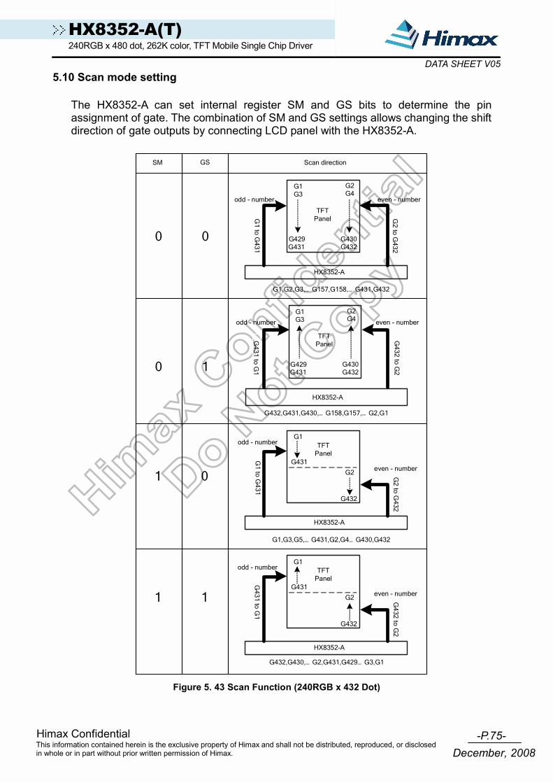
-P.75- Himax Confidential
December, 2008This information contained herein is the exclusive property of Himax and shall not be distributed, reproduced, or disclosed in whole or in part without prior written permission of Himax.
HX8352-A(T) 240RGB x 480 dot, 262K color, TFT Mobile Single Chip Driver
DATA SHEET V055.10 Scan mode setting
The HX8352-A can set internal register SM and GS bits to determine the pin assignment of gate. The combination of SM and GS settings allows changing the shift direction of gate outputs by connecting LCD panel with the HX8352-A.
0 0
HX8352-A
odd - number
TFT PanelG
1to
G431
Scan directionSM GS
even - number
G1G3
G429G431
G2G4
G430G432
G2
toG
432
0 1
HX8352-A
odd - number even - number
G431
toG
1
G432
toG
2
TFT Panel
G1G3
G429G431
G2G4
G430G432
G1,G2,G3,… G157,G158,… G431,G432
G432,G431,G430,… G158,G157,… G2,G1
1 0
HX8352-A
odd - number TFT Panel
G1
toG
431
even - number
G1
G431
G2
G432
G2
toG
432
G1,G3,G5,… G431,G2,G4… G430,G432
1 1
HX8352-A
odd - number TFT Panel
G431
toG
1
even - number
G1
G431
G2
G432
G4
32to
G2
G432,G430,… G2,G431,G429… G3,G1
Figure 5. 43 Scan Function (240RGB x 432 Dot)

-P.76- Himax Confidential
December, 2008This information contained herein is the exclusive property of Himax and shall not be distributed, reproduced, or disclosed in whole or in part without prior written permission of Himax.
HX8352-A(T) 240RGB x 480 dot, 262K color, TFT Mobile Single Chip Driver
DATA SHEET V055.11 Register setting flow
The following are the sequences of register setting flow that applied to the HX8352-A driving the TFT display, when operate in Register-Content interface mode. Display on/off set flow
Display off flow Display on flow
Display offGON = "1"DTE = "1"D1-0 = "10"
Wait 2 frames or more
Display offGON = "1"DTE = "0"D1-0 = "10"
Display offGON = "1"DTE = "0"D1-0 = "00"
Power OFF SettingN_SAP[7-0] = "00000000"AP[2-0] ="000"PON ="0"
VCOMG = "0"
"Display off"
"Display on"
Display onGON = "1"DTE = "1"D1-0 = "10"
Wait 2 frames or more
N_SAP[7-0] Set
Display onGON = "1"DTE = "1"D1-0 = "11"
Power ON setting
Wait 2 frames or more
DK ="1"
Figure 5. 44 Display On/Off Set Sequence

-P.77- Himax Confidential
December, 2008This information contained herein is the exclusive property of Himax and shall not be distributed, reproduced, or disclosed in whole or in part without prior written permission of Himax.
HX8352-A(T) 240RGB x 480 dot, 262K color, TFT Mobile Single Chip Driver
DATA SHEET V05
Standby mode set flow
Figure 5. 45 Standby Mode Setting Sequence
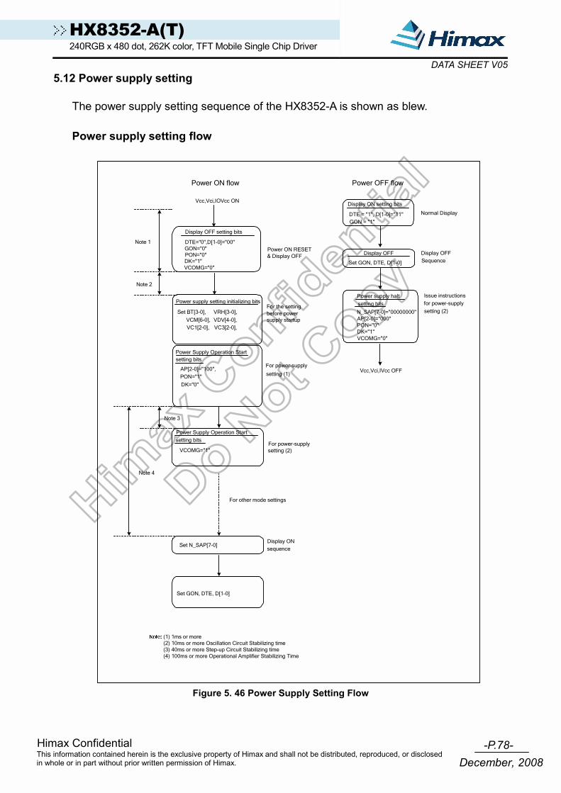
-P.78- Himax Confidential
December, 2008This information contained herein is the exclusive property of Himax and shall not be distributed, reproduced, or disclosed in whole or in part without prior written permission of Himax.
HX8352-A(T) 240RGB x 480 dot, 262K color, TFT Mobile Single Chip Driver
DATA SHEET V055.12 Power supply setting
The power supply setting sequence of the HX8352-A is shown as blew. Power supply setting flow
Power ON RESET & Display OFF
DTE="0",D[1-0]="00"
For power-supply
setting (1)AP[2-0]="100",
Set BT[3-0], VRH[3-0],
VCM[6-0], VDV[4-0],
PON="0"
VCOMG="0"
Display ONsequence
VC1[2-0],
PON="1"
VCOMG="1"
GON="0"
Set N_SAP[7-0]
Power Supply Operation Startsetting bits
Display OFF setting bits
Power Supply Operation Start
setting bits
For other mode settings
For power-supplysetting (2)
For the settingbefore powersupply startup
Power supply setting initializing bits
(1) 1ms or more (2) 10ms or more Oscillation Circuit Stabilizing time (3) 40ms or more Step-up Circuit Stabilizing time (4) 100ms or more Operational Amplifier Stabilizing Time
Note 1
Note 2
Note 3
Note 4
Vcc,Vci,IOVcc ON
DK="1"
Set GON, DTE, D[1-0]
Display OFFSequence
Display OFF
Normal DisplayDTE = "1", D[1-0]="11"GON = "1"
Display ON setting bits
Power OFF flow
AP[2-0]="000"PON="0"
N_SAP[7-0]="00000000"
VCOMG="0"
Issue instructions
for power-supply
setting (2)
Power supply halt
setting bits
Vcc,Vci,IVcc OFF
DK="1"
Set GON, DTE, D[1-0]
Power ON flow
VC3[2-0],
DK="0"
Figure 5. 46 Power Supply Setting Flow

-P.79- Himax Confidential
December, 2008This information contained herein is the exclusive property of Himax and shall not be distributed, reproduced, or disclosed in whole or in part without prior written permission of Himax.
HX8352-A(T) 240RGB x 480 dot, 262K color, TFT Mobile Single Chip Driver
DATA SHEET V055.13 OTP programming
OTP_INDEX D7 D6 D5 D4 D3 D2 D1 D0 00h Himax Internal use 01h (no use) Himax Internal use 02h Himax Internal use 03h (no use) Himax Internal use 04h Himax Internal use 05h (no use) Himax Internal use 06h Himax Internal use 07h (no use) Himax Internal use 08h Himax Internal use 09h Himax Internal use 0Ah Himax Internal use 0Bh (no use) 0Ch (no use) Himax Internal use 0Dh Himax Internal use Himax Internal use (no use) 0Eh Himax Internal use 0Fh NVALID1 (no use) Himax Internal use 10h (no use) Himax Internal use 11h (no use) VDV[4:0] 12h NVALID2 VCM[6:0] 13h (no use) Himax Internal use 14h (no use) Himax Internal use 15h (no use) Himax Internal use 16h (no use) Himax Internal use 17h (no use) Himax Internal use 18h (no use) Himax Internal use 19h (no use) Himax Internal use 1Ah (no use) Himax Internal use 1Bh (no use) Himax Internal use 1Ch (no use) Himax Internal use 1Dh (no use) Himax Internal use 1Eh (no use) Himax Internal use 1Fh (no use) Himax Internal use 20h (no use) Himax Internal use 21h (no use) Himax Internal use 22h (no use) Himax Internal use 23h (no use) Himax Internal use 24h (no use) Himax Internal use 25h (no use) Himax Internal use 26h (no use) Himax Internal use 27h (no use) Himax Internal use 28h (no use) Himax Internal use 29h (no use) Himax Internal use 2Ah (no use) Himax Internal use 2Bh (no use) Himax Internal use 2Ch (no use) Himax Internal use 2Dh (no use) Himax Internal use 2Eh (no use) Himax Internal use 2Fh (no use) Himax Internal use 30h Himax Internal use 31h NVALID4 Himax Internal use 32h Himax Internal use
33h NVALID3 (no use) Internal use
34h (no use) Himax Internal use (no use) 35h (no use) VDV[4:0] 36h NVALID5 VCM[6:0] 37h (no use) VDV[4:0] 38h NVALID6 VCM[6:0]
Note: NVALID1~6 are control differential banks. (1) NVALID1: Control Bank1 (00h ~ 10h). (2) NVALID2: Control Bank1 (11h ~ 12h). (3) NVALID3: Control Bank1 (13h ~ 2Fh, 33h~34h). (4) NVALID4: Control Bank1 (30h ~ 32h). (5) NVALID5: Control Bank1 (35h ~ 36h). (6) NVALID6: Control Bank1 (37h ~ 38h). NVALIDx: 1 -> Not reload data of OTP to register; 0 -> Need reload data of OTP to register.
Table 5. 26 OTP Memory Table

-P.80- Himax Confidential
December, 2008This information contained herein is the exclusive property of Himax and shall not be distributed, reproduced, or disclosed in whole or in part without prior written permission of Himax.
HX8352-A(T) 240RGB x 480 dot, 262K color, TFT Mobile Single Chip Driver
DATA SHEET V05Programming flow
Standby Off
Set DCCLK_DISABLE=1
Wait for VGH becoming
2.78V
Tie VGH to 7.5V
Write optimized value into registers
Set OTP_INDEX
Set OTP_PROG=1
Wait for 1ms
Wait for 100ms
Figure 5. 47 OTP Programming Flow
Programming circuitry

-P.81- Himax Confidential
December, 2008This information contained herein is the exclusive property of Himax and shall not be distributed, reproduced, or disclosed in whole or in part without prior written permission of Himax.
HX8352-A(T) 240RGB x 480 dot, 262K color, TFT Mobile Single Chip Driver
DATA SHEET V05Programming sequence
Step Operation
1 Power on and reset the module 2 Set OTP_LOAD_DISABLE=1, disable the auto-loading function. 3 OSC_EN=1, STB=0 4 Wait 120ms
5
Write optimized value to related register Command Register Description
OSC Control1 (17h) RADJ[3:0] The division ratio of clocks in display modeIP control (5Ah) DGC_EN DGC function Disable/Enable
VCOM Control (1Fh) VCM[6:0] VcomH voltage (High level voltage of VCOM)
Power Control1 (1Eh) VDV[4:0] Vcom amplitude (VcomL = VcomH – Vcomamplitude, VcomL ≥ VCL+0.5V)
PANEL Control Register (R55h)
BGR_PANEL, SM_PANEL, SS_PANEL, GS_PANEL, REV_PANEL
PANEL Control
Note: ID1~ID3 are don’t care in Register-Content Interface mode. 6 Set OTP_ DCCLK_DISABLE=1, disable internal pumping clock. 7 Wait 500ms for power down 8 Connect external power 7.5V to VGH pin 9 Wait 100ms for VGH stable
10
Specify OTP_index OTP_index Parameter
0x10h RADJ[3:0] 0x11h VDV[4:0] 0x12h VCM[6:0 0x13h BGR_PANEL, SM_PANEL, SS_PANEL, GS_PANEL, REV_PANEL 0x33h DGC_EN
11 Set OTP_Mask=0x00h, programming the entire bit of one parameter. 12 Set OTP_PROG=1, Internal register begin write to OTP according to OTP_index. 13 Wait 1 ms
14 Complete programming one parameter to OTP. If continue to programming other parameter, set OTP_PROG=0 before return to step (9). Otherwise, power off the module and remove the external power on VGH pin.

-P.82- Himax Confidential
December, 2008This information contained herein is the exclusive property of Himax and shall not be distributed, reproduced, or disclosed in whole or in part without prior written permission of Himax.
HX8352-A(T) 240RGB x 480 dot, 262K color, TFT Mobile Single Chip Driver
DATA SHEET V05
5.14 Free running mode specification
Burn-in of TFT displays consists of driving each module for 10hr at a temperature of 60°C. In order to drive the modules, it requires extra electronics. To reduce the burn-in cost, it is requested that the driver IC will generate the required display image without requiring extra electronics. We term this a free running mode (FR-mode). For burn-in, it is sufficient that the display is powered up with a plane saturated black or saturated white pattern. Black should be used for burn-in, since this result in a larger pixel voltage. White is used to verify if the free running mode is properly functioning. Please note that the black and the white pattern are reversed in case of a normally black display.
Parameter Symbol Description
Power supply pins IOVCC, VCI, VCC All power supply pins Free running mode BURN BURN=1, FR-mode is enabled. Reset NRESET Active low pulse in order to start the FR-mode. Chip select(1) NCS This pin will be left open during FRM mode. Data enable(1) ENABLE This pin will be left open during FRM mode. Reads/not write(1) NRD_E, WR_RNW This pin will be left open during FRM mode. Data/not command(1) DNC_SCL This pin will be left open during FRM mode. Horizontal sync(1) HSYNC This pin will be left open during FRM mode. Vertical sync(1) VSYNC This pin will be left open during FRM mode. Data clock DOTCLK This pin will be left open during FRM mode. CPU I/F Data(1) DB[0..17] This pin will be left open during FRM mode. SPI I/F Data(1) SDI, SDO This pin will be left open during FRM mode.
Note: (1) The BURN-pin has a pull down resistor inside the driver IC, because this pin will be left open during the normal operation in the application. The BURN-pin must be logical high for longer than 5ms before the driver IC will switch to the FR-mode in order to avoid disturbances during normal operation.
(2) As a general rule, all control pins of the interfaces like chip-select, data-enable, etc must be disabled, all mode select pins like data-not-command, interface-select etc and all data-bus pins must be set to eider logic high or logic low during the FR-mode.
Table 5. 27 Pin Information of Free Running Mode

-P.83- Himax Confidential
December, 2008This information contained herein is the exclusive property of Himax and shall not be distributed, reproduced, or disclosed in whole or in part without prior written permission of Himax.
HX8352-A(T) 240RGB x 480 dot, 262K color, TFT Mobile Single Chip Driver
DATA SHEET V05
Power-on sequence
The FR-mode starts automatically after the power supply is switched on and a reset pulse is applied to the Reset-pin, if the BURN pin is set to logical high. In case of separate supply pins for the analogue supply and digital supply, both supply pins will be connected together, if it is supported by the driver specification. Otherwise, each supply voltage will be switched on separately according to the requested power-on sequence. The BURN and all other digital I/F pins, which will be set to logic high during the free running mode, can be switched to logic high together with the digital supply pin. The FR-mode will be restarted if the reset pulse is applied a second time. The OTP starts to load when Reset leaves low to high.
White
tWhite
VCC, VCI
BURN
Mclk (Option)
Display
Reset
t
White
t Resett FRM-Rese
OTPLoad
OTP Start Load
Black Black
t(VCC, VCI)-FRM
tBlacktReset-on
tAlternating
Black
t(VCC, VCI)-Mclk
Figure 5. 48 Power On Sequence of FR-mode (for Normally–White Panel)
Power off sequence The power supply can be switched off any time.
VCC, VCI
BURN
Mdk (Option)
Figure 5. 49 Power Off Sequence of FR-mode

-P.84- Himax Confidential
December, 2008This information contained herein is the exclusive property of Himax and shall not be distributed, reproduced, or disclosed in whole or in part without prior written permission of Himax.
HX8352-A(T) 240RGB x 480 dot, 262K color, TFT Mobile Single Chip Driver
DATA SHEET V05
Free running mode display The display will show an alternating black and white picture for about the first 5 minutes. The black to white ratio shell be 50%. The time of the black and white pattern shell is around 1 second in order to avoid a too long waiting time to verify that the FR-mode is functioning properly. The display is switched to a static black pattern after the alternating mode is finished. Thus, most efficient burn-in stress is ensured. The display shall work in idle-mode. There is no special restriction for the frame frequency. It can be between 5 and 100Hz. The frame frequency will be set according to the parameter in the OTP.
Alternating Black and White Pattern tAlternating - 5 - min Master Clock Frequency fMclk - - 10 MHz
Table 5. 28 Frequency Definition of Free Running Mode Display
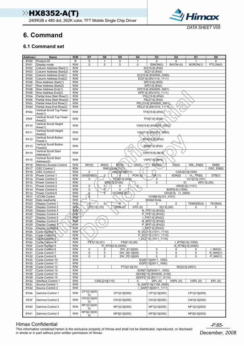
-P.85- Himax Confidential
December, 2008This information contained herein is the exclusive property of Himax and shall not be distributed, reproduced, or disclosed in whole or in part without prior written permission of Himax.
HX8352-A(T) 240RGB x 480 dot, 262K color, TFT Mobile Single Chip Driver
DATA SHEET V05
6. Command 6.1 Command set Address Name R/W D7 D6 D5 D4 D3 D2 D1 D0
8'h00 Product ID R 0 1 0 1 0 0 1 0 8'h01 Display mode R/W 0 0 0 0 IDMON(0) INVON (0) NORON(1) PTLON(0)8'h02 Column Address Start(1) R/W SC[15:8] (8'b0) 8'h03 Column Address Start(2) R/W SC[7:0] (8'b0) 8'h04 Column Address End(1) R/W EC[15:8] (8'b0000_0000) 8'h05 Column Address End(2) R/W EC[7:0] (8'b1110_1111) 8'h06 Row Address Start(1) R/W SP[15:8] (8'b0) 8'h07 Row Address Start(2) R/W SP[7:0] (8'b0) 8'h08 Row Address End(1) R/W EP[15:8] (8'b0000_0001) 8'h09 Row Address End(2) R/W EP[7:0] (8'b1010_1111) 8'h0a Partial Area Start Row(1) R/W PSL[15:8] (8'b0) 8'h0b Partial Area Start Row(2) R/W PSL[7:0] (8'b0) 8'h0c Partial Area End Row(1) R/W PEL[15:8] (8'b0000_0001) 8'h0d Partial Area End Row(2) R/W PEL[7:0] (8'b1010_1111)
8'h0e Vertical Scroll Top Fixed Area(1) R/W TFA[15:8] (8'b0)
8'h0f Vertical Scroll Top Fixed Area(2) R/W TFA[7:0] (8'b0)
8'h10 Vertical Scroll Height Area(1) R/W VSA[15:8] (8'b0000_0001)
8'h11 Vertical Scroll Height Area(2) R/W VSA[7:0] (8'b1011_0000)
8'h12 Vertical Scroll Button Fixed(1) R/W BFA[15:8] (8'b0)
8'h13 Vertical Scroll Button Fixed(2) R/W BFA[7:0] (8'b0)
8'h14 Vertical Scroll Start Address(1) R/W VSP[15:8] (8b’0)
8'h15 Vertical Scroll Start Address(2) R/W VSP[7:0] (8b’0)
8'h16 Memory Access Control R/W MY(0) MX(0) MV(0) GS(0) BGR(0) SS(0) SRL_EN[0] SM[0] 8'h17 OSC Control 1 R/W RADJ[3:0](1111) OSC_EN[0]8'h18 OSC Control 2 R/W 0 UADJ[2:0](011) CADJ[3:0](1000) 8'h19 Power Control 1 R/W GASENB(0) 0 0 PON (0) DK (1) XDK[0] VL_TRI[0] STB[1] 8'h1a Power Control 2 R/W 0 VC3[2:0] (000) 0 VC1[2:0] (101) 8'h1b Power Control 3 R/W BT[3:0] (0100) 0 0 AP[1:0] (00) 8'h1c Power Control 4 R/W 0 0 0 0 VRH[3:0] (1101) 8'h1d Power Control 5 R/W 0 0 0 BGP[3:0] (1000) 8'h1e Power Control 6 R/W 0 0 VCOMG (0) VDV[4:0] (1_0000) 8'h1f VCOM Control R/W 0 VCM[6:0](101_0101) 8'h22 Data read/write R/W SRAM Write 8'h23 Display Control 1 R/W 0 0 0 0 0 0 TEMODE(0) TEON(0) 8'h24 Display Control 2 R/W PT[1:0] (10) GON (1) DTE (0) D[1:0] (00) 0 0 8'h25 Display Control 3 R/W N_FP[7:0] (8'h02) 8'h26 Display Control 4 R/W P_FP[7:0] (8'h02) 8'h27 Display Control 5 R/W I_FP[7:0] (8'h02) 8'h28 Display Control 6 R/W N_BP[7:0] (8'h02) 8'h29 Display Control 7 R/W P_BP[7:0] (8'h02) 8'h2a Display Control 8 R/W I_BP[7:0] (8'h02) 8'h2b Cycle Control 1 R/W N_DC[7:0] (1011_1110) 8'h2c Cycle Control 2 R/W P_DC[7:0] (1011_1110) 8'h2d Cycle Control 3 R/W I_DC[7:0] (1011_1110) 8'h2e Cycle Control 4 R/W FS1[1:0] (01) FS0[1:0] (00) I_RTN[3:0] (1000) 8'h2f Cycle Control 5 R/W PI_RTN[3:0] (0000) N_RTN[3:0] (0000) 8'h30 Cycle Control 6 R/W 0 0 DIV_I[1:0](00) 0 0 0 I_NW(0) 8'h31 Cycle Control 7 R/W 0 0 DIV_N[1:0](00) 0 0 0 N_NW](1) 8'h32 Cycle Control 8 R/W 0 0 DIV_P[1:0](00) 0 0 0 P_NW(1) 8'h34 Cycle Control 10 R/W EQS[7:0](0011_1000) 8'h35 Cycle Control 11 R/W EQP[7:0](0011_1000) 8'h36 Cycle Control 12 R/W PTG[1:0](10) ISC[3:0] (0001) 8'h37 Cycle Control 13 R/W SON[7:0](8'b0011_1000) 8'h38 Cycle Control 14 R/W GDON[7:0] (8'b0000_0100) 8'h39 Cycle Control 15 R/W GDOF[7:0] (8'b1111_0110) 8'h3a Interface Control 1 R/W CSEL[2:0](110) 0 DPL (0) HSPL (0) VSPL (0) EPL (0) 8'h3c Source Control 1 R/W N_SAP[7:0](1100_0000) 8'h3d Source Control 2 R/W I_SAP[7:0](0011_1111)
8'h3e Gamma Control 1 R/W CP1[2:0](000) CP1[2:0](000) CP1[2:0](000) CP1[2:0](000)
8'h3f Gamma Control 2 R/W CN1[2:0](000) CN1[2:0](000) CN1[2:0](000) CN1[2:0](000)
8'h40 Gamma Control 3 R/W NP1[2:0](000) NP1[2:0](000) NP1[2:0](000) NP1[2:0](000)
8'h41 Gamma Control 4 R/W NP3[2:0](000) NP3[2:0](000) NP3[2:0](000) NP3[2:0](000)

-P.86- Himax Confidential
December, 2008This information contained herein is the exclusive property of Himax and shall not be distributed, reproduced, or disclosed in whole or in part without prior written permission of Himax.
HX8352-A(T) 240RGB x 480 dot, 262K color, TFT Mobile Single Chip Driver
DATA SHEET V05Address Name R/W D7 D6 D5 D4 D3 D2 D1 D0
8'h42 Gamma Control 5 R/W NP5[2:0](000) NP5[2:0](000) NP5[2:0](000) NP5[2:0](000)
8'h43 Gamma Control 6 R/W NN1[2:0](000) NN1[2:0](000) NN1[2:0](000) NN1[2:0](000)
8'h44 Gamma Control 7 R/W NN3[2:0](000) NN3[2:0](000) NN3[2:0](000) NN3[2:0](000)
8'h45 Gamma Control 8 R/W NN5[2:0](000) NN5[2:0](000) NN5[2:0](000) NN5[2:0](000)
8'h46 Gamma Control 9 R/W CGMP1[1:0](00) CGMP1[1:0](00) CGMP1[1:0](00) 8'h47 Gamma Control 10 R/W CGMP2 CGMP2 CGMP2 CGMP2 8'h48 Gamma Control 11 R/W CGMN1[1:0](00) CGMN1[1:0](00) CGMN1[1:0](00) 8'h49 Gamma Control 12 R/W CGMN2 CGMN2 CGMN2 CGMN2
8'h55 PANEL Control R/W 0 0 0 SM_PANEL(0) SS_PANEL(0) GS_PANEL(
0) REV_PANEL(
0) BGR_PANEL(
0) 8'h56 OTP 1 R/W OTP_INDEX[7:0] (8'b1111_1111) 8'h57 OTP 2 R/W OTP_MASK[7:0] (8'b0)
8'h58 OTP 3 R/W DCCLK_ DISABLE
(0)
DCCLK_ DISABLE
(0)
DCCLK_ DISABLE
(0)
DCCLK_ DISABLE (0) OTP_PTM (0) 0 VPP_SEL (0) OTP_PROG
(0)
8'h59 OTP 4 R OTP_DATA[7:0] 8'h5a IP Control R/W 0 0 0 0 0 0 0 DGC_EN(0)8'h5c DGC LUT WRITE R/W LUT[7:0](8'b0) 8'h5d DATA Control R/W 0 0 0 0 DFM[1:0](00) TRI[1:0](00) 8’h83 Test Mode R/W 0 0 0 0 0 0 TEST_Mode 0 8’h85 VDDD control R/W 0 0 0 0 0 VDC_SEL[2:0] (101) 8’h8A Powr driving Control R/W 0 0 0 0 0 PTBA[2:0] (110) 8’h8B VGS_RES control 1 R/W 0 0 0 0 0 0 0 RES_VGS18’h8C VGS_RES control 2 R/W RES_VGS0 0 0 1 0 0 1 1 8’h91 PWM Control 3 R/W 0 0 0 0 0 0 0 SYNC 8’h95 PWM Control 1 R/W DBV[7:0] 8’h96 PWM Control 2 R/W 0 0 BCTRL 0 0 BL 0 0 8’h97 PWM Control 3 R/W 0 0 0 0 0 0 C1 C0 8’h6B CABC Period Control 1 R/W 1 1 1 0 1 SEL_PWMCLK[2:0] (3’b000) 8’h6C CABC Period Control 2 R/W PWM_PERIOD (8’b0101_0100) 8’h6F CABC Gain1 R/W 0 BGG0(6:0) (7’b100_0000) 8’h70 CABC Gain2 R/W 0 BGG1(6:0) (7’b011_0000) 8’h71 CABC Gain3 R/W 0 BGG2(6:0) (7’b010_1010) 8’h72 CABC Gain4 R/W 0 BGG3(6:0) (7’b010_1000) 8’h73 CABC Gain5 R/W 0 BGG4(6:0) (7’b010_0110) 8’h74 CABC Gain6 R/W 0 BGG5(6:0) (7’b010_0100) 8’h75 CABC Gain7 R/W 0 BGG6(6:0) (7’b010_0010) 8’h76 CABC Gain8 R/W 0 BGG7(6:0) (7’b010_0001) 8’h77 CABC Gain9 R/W 0 BGG8(6:0) (7’b000_0010)

-P.87- Himax Confidential
December, 2008This information contained herein is the exclusive property of Himax and shall not be distributed, reproduced, or disclosed in whole or in part without prior written permission of Himax.
HX8352-A(T) 240RGB x 480 dot, 262K color, TFT Mobile Single Chip Driver
DATA SHEET V05
6.2 Index register
Figure 6. 1 Index Register
Index register (IR) specifies Index of the register from R00h to RFFh. It sets the register number (ID7-0) in the range from 000000b to 1111111b in binary form.
6.3 Producet ID register (R00h)
Figure 6. 2 Product ID Register (R00h)
Product ID: 0x52h 6.4 Display mode control register (R01h)
Figure 6. 3 Display Mode Control Register (R01h)
IDMON: This command is used for turning on/off IDLE (8-color display) mode by setting IDMON=1/0. Note: IDLE ON do not support Digital Gamma used.
INVON: This command is used to enter into display inversion mode by setting INVON=1. Vise versa, it recovers from display inversion mode by setting INVON=0. This command makes no change of contents of frame memory. Every bit is inverted from the frame memory to the display. This command does not change any other status.
NORON: This command is used for turning on/off NORMAL mode by setting NORON=1/0.
PTLON: This command is used for turning on/off PARTIAL mode by setting PTLON=1/0.

-P.88- Himax Confidential
December, 2008This information contained herein is the exclusive property of Himax and shall not be distributed, reproduced, or disclosed in whole or in part without prior written permission of Himax.
HX8352-A(T) 240RGB x 480 dot, 262K color, TFT Mobile Single Chip Driver
DATA SHEET V05
6.5 Column address start register (R02~03h)
Figure 6. 4 Column Address Start Register Upper Byte (R02h)
Figure 6. 5 Column Address Start Register Low Byte (R03h)
6.6 Column address end register (R04~05h)
Figure 6. 6 Column Address End Register Upper Byte (R04h)
Figure 6. 7 Column Address End Register Low Byte (R05h)
6.7 Row address start register (R06~07h)
Figure 6. 8 Row Address Start Register Upper Byte (R06h)
Figure 6. 9 Row Address Start Register Low Byte (R07h)
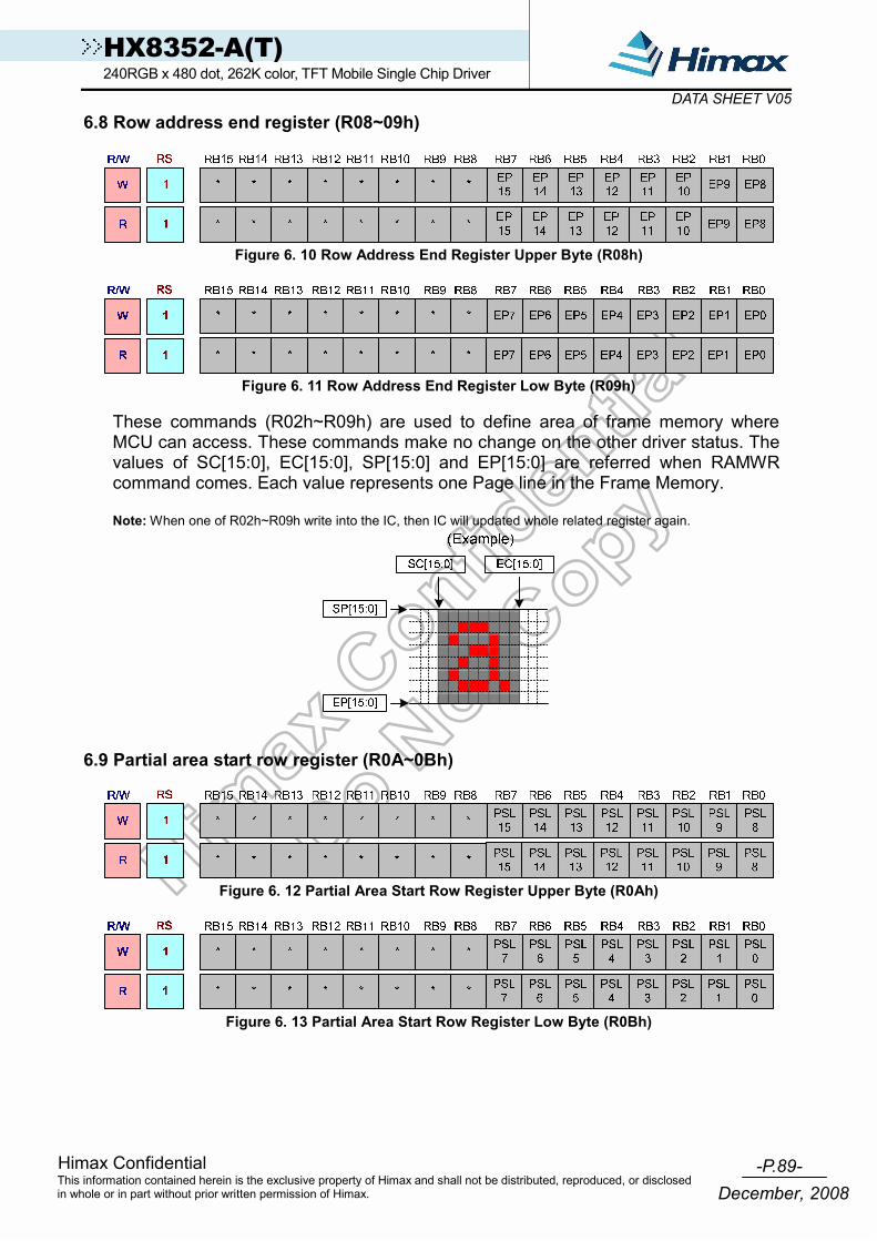
-P.89- Himax Confidential
December, 2008This information contained herein is the exclusive property of Himax and shall not be distributed, reproduced, or disclosed in whole or in part without prior written permission of Himax.
HX8352-A(T) 240RGB x 480 dot, 262K color, TFT Mobile Single Chip Driver
DATA SHEET V05
6.8 Row address end register (R08~09h)
Figure 6. 10 Row Address End Register Upper Byte (R08h)
Figure 6. 11 Row Address End Register Low Byte (R09h)
These commands (R02h~R09h) are used to define area of frame memory where MCU can access. These commands make no change on the other driver status. The values of SC[15:0], EC[15:0], SP[15:0] and EP[15:0] are referred when RAMWR command comes. Each value represents one Page line in the Frame Memory. Note: When one of R02h~R09h write into the IC, then IC will updated whole related register again.
6.9 Partial area start row register (R0A~0Bh)
Figure 6. 12 Partial Area Start Row Register Upper Byte (R0Ah)
Figure 6. 13 Partial Area Start Row Register Low Byte (R0Bh)

-P.90- Himax Confidential
December, 2008This information contained herein is the exclusive property of Himax and shall not be distributed, reproduced, or disclosed in whole or in part without prior written permission of Himax.
HX8352-A(T) 240RGB x 480 dot, 262K color, TFT Mobile Single Chip Driver
DATA SHEET V05
6.10 Partial area end row register (R0C~0Dh)
Figure 6. 14 Partial Area End Row Register Upper Byte (R0Ch)
Figure 6. 15 Partial Area End Row Register Low Byte (R0Dh)
These commands (R0Ah~~0Dh) define the partial mode’s display area. There are 4 parameters associated with this command, PSL[15:0], PEL[15:0], as illustrated in the figures below. PSL and PEL refer to the Frame Memory Line Pointer.
If End Row>Start Row when Memory Access Control GS=0
PSL [15:0]
PEL[15:0]
Start Row
End Row
Partial Display Area
If End Row>Start Row when Memory Access Control GS=1
PEL [15:0]
PSL [15:0]
End Row
Start Row
Partial Display Area
If End Row<Start Row when Memory Access Control GS=0
If End Row = Start Row then the Partial Area will be one row deep.
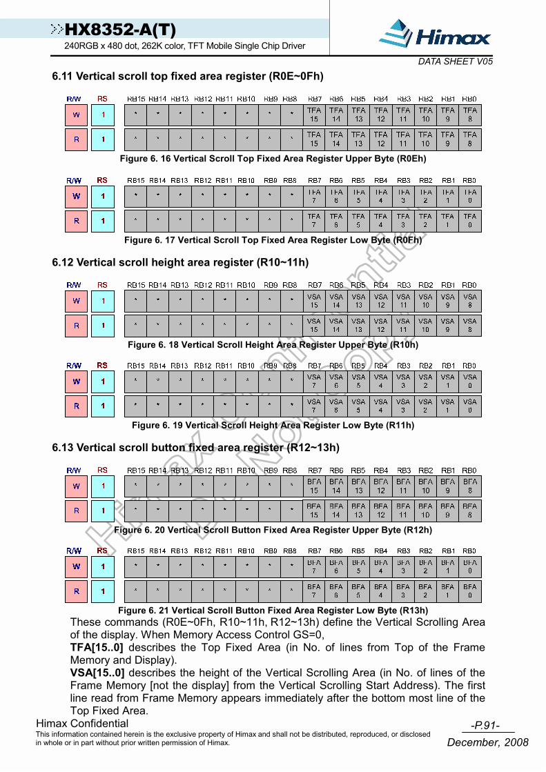
-P.91- Himax Confidential
December, 2008This information contained herein is the exclusive property of Himax and shall not be distributed, reproduced, or disclosed in whole or in part without prior written permission of Himax.
HX8352-A(T) 240RGB x 480 dot, 262K color, TFT Mobile Single Chip Driver
DATA SHEET V05
6.11 Vertical scroll top fixed area register (R0E~0Fh)
Figure 6. 16 Vertical Scroll Top Fixed Area Register Upper Byte (R0Eh)
Figure 6. 17 Vertical Scroll Top Fixed Area Register Low Byte (R0Fh)
6.12 Vertical scroll height area register (R10~11h)
Figure 6. 18 Vertical Scroll Height Area Register Upper Byte (R10h)
Figure 6. 19 Vertical Scroll Height Area Register Low Byte (R11h)
6.13 Vertical scroll button fixed area register (R12~13h)
Figure 6. 20 Vertical Scroll Button Fixed Area Register Upper Byte (R12h)
Figure 6. 21 Vertical Scroll Button Fixed Area Register Low Byte (R13h)
These commands (R0E~0Fh, R10~11h, R12~13h) define the Vertical Scrolling Area of the display. When Memory Access Control GS=0, TFA[15..0] describes the Top Fixed Area (in No. of lines from Top of the Frame Memory and Display). VSA[15..0] describes the height of the Vertical Scrolling Area (in No. of lines of the Frame Memory [not the display] from the Vertical Scrolling Start Address). The first line read from Frame Memory appears immediately after the bottom most line of the Top Fixed Area.
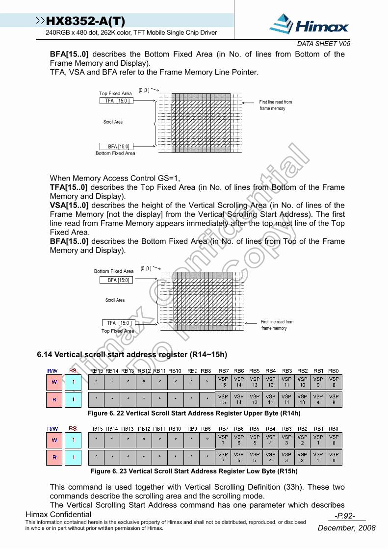
-P.92- Himax Confidential
December, 2008This information contained herein is the exclusive property of Himax and shall not be distributed, reproduced, or disclosed in whole or in part without prior written permission of Himax.
HX8352-A(T) 240RGB x 480 dot, 262K color, TFT Mobile Single Chip Driver
DATA SHEET V05
BFA[15..0] describes the Bottom Fixed Area (in No. of lines from Bottom of the Frame Memory and Display). TFA, VSA and BFA refer to the Frame Memory Line Pointer.
(0 ,0 )
TFA [15:0 ]
BFA [15:0]
Scroll Area
First line read fromframe memory
Top Fixed Area
Bottom Fixed Area
When Memory Access Control GS=1, TFA[15..0] describes the Top Fixed Area (in No. of lines from Bottom of the Frame Memory and Display). VSA[15..0] describes the height of the Vertical Scrolling Area (in No. of lines of the Frame Memory [not the display] from the Vertical Scrolling Start Address). The first line read from Frame Memory appears immediately after the top most line of the Top Fixed Area. BFA[15..0] describes the Bottom Fixed Area (in No. of lines from Top of the Frame Memory and Display).
(0 ,0 )
Scroll Area
First line read fromframe memoryTop Fixed Area
Bottom Fixed Area
TFA [15:0 ]
BFA [15:0]
6.14 Vertical scroll start address register (R14~15h)
Figure 6. 22 Vertical Scroll Start Address Register Upper Byte (R14h)
Figure 6. 23 Vertical Scroll Start Address Register Low Byte (R15h)
This command is used together with Vertical Scrolling Definition (33h). These two commands describe the scrolling area and the scrolling mode. The Vertical Scrolling Start Address command has one parameter which describes

-P.93- Himax Confidential
December, 2008This information contained herein is the exclusive property of Himax and shall not be distributed, reproduced, or disclosed in whole or in part without prior written permission of Himax.
HX8352-A(T) 240RGB x 480 dot, 262K color, TFT Mobile Single Chip Driver
DATA SHEET V05
the address of the line in the Frame Memory that will be written as the first line after the last line of the Top Fixed Area on the display as illustrated below: When Memory Access Control B4=0
Example: When Top Fixed Area = Bottom Fixed Area = 00, Vertical Scrolling Area = 162 and VSP=3
When Memory Access Control B4=1 Example: When Top Fixed Area = Bottom Fixed Area = 00, Vertical Scrolling Area = 162 and VSP=3
When new Pointer position and Picture Data are sent, the result on the display will happen at the next Panel Scan to avoid tearing effect. VSP refers to the Frame Memory line Pointer.
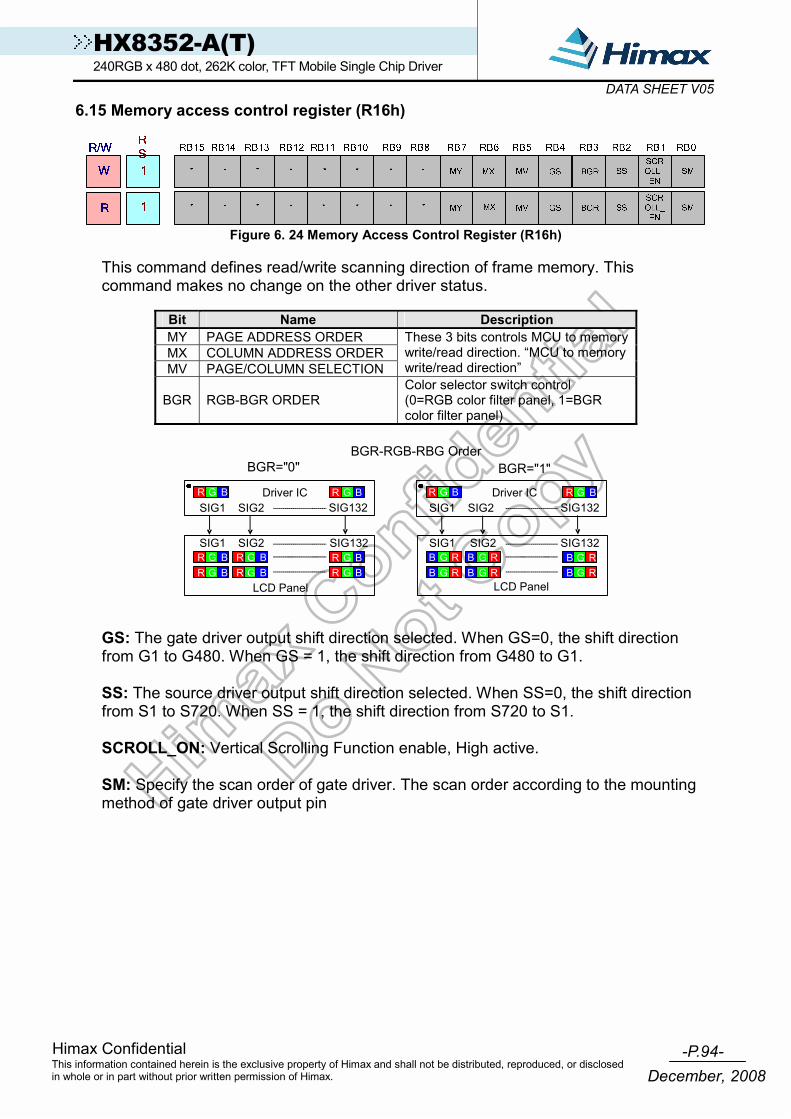
-P.94- Himax Confidential
December, 2008This information contained herein is the exclusive property of Himax and shall not be distributed, reproduced, or disclosed in whole or in part without prior written permission of Himax.
HX8352-A(T) 240RGB x 480 dot, 262K color, TFT Mobile Single Chip Driver
DATA SHEET V05
6.15 Memory access control register (R16h)
Figure 6. 24 Memory Access Control Register (R16h)
This command defines read/write scanning direction of frame memory. This command makes no change on the other driver status.
Bit Name Description MY PAGE ADDRESS ORDER MX COLUMN ADDRESS ORDER MV PAGE/COLUMN SELECTION
These 3 bits controls MCU to memory write/read direction. “MCU to memory write/read direction”
BGR RGB-BGR ORDER Color selector switch control (0=RGB color filter panel, 1=BGR color filter panel)
BGR="0" BGR="1"
R G B R G BSIG1 SIG132
Driver IC
LCD Panel
R G B R G BR G B R G B
R G BR G B
SIG1 SIG132SIG2
SIG2R G B R G BSIG1 SIG132
Driver IC
LCD Panel
B G R B G RB G R B G R
B G RB G R
SIG1 SIG132SIG2
SIG2
BGR-RGB-RBG Order
GS: The gate driver output shift direction selected. When GS=0, the shift direction from G1 to G480. When GS = 1, the shift direction from G480 to G1. SS: The source driver output shift direction selected. When SS=0, the shift direction from S1 to S720. When SS = 1, the shift direction from S720 to S1. SCROLL_ON: Vertical Scrolling Function enable, High active. SM: Specify the scan order of gate driver. The scan order according to the mounting method of gate driver output pin

-P.95- Himax Confidential
December, 2008This information contained herein is the exclusive property of Himax and shall not be distributed, reproduced, or disclosed in whole or in part without prior written permission of Himax.
HX8352-A(T) 240RGB x 480 dot, 262K color, TFT Mobile Single Chip Driver
DATA SHEET V05
6.16 OSC control 1 register (R17h)
Figure 6. 25 OSC Control 1 Register (R17h)
This command is used to set internal oscillator related setting RADJ[3:0]: Internal oscillator frequency adjust, default is 7.5MHz.
RADJ3 RADJ2 RADJ1 RADJ0 Internal Oscillator Frequency 0 0 0 0 145% 0 0 0 1 140% 0 0 1 0 135% 0 0 1 1 130% 0 1 0 0 125% 0 1 0 1 120% 0 1 1 0 115% 0 1 1 1 110% 1 0 0 0 105% 1 0 0 1 100% 1 0 1 0 95% 1 0 1 1 90% 1 1 0 0 85% 1 1 0 1 80% 1 1 1 0 75% 1 1 1 1 70%
OSC_EN: Enable internal oscillator, High active.
6.17 OSC control 2 register (R18h)
Figure 6. 26 OSC Control 2 Register (R18h)
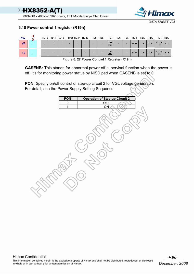
-P.96- Himax Confidential
December, 2008This information contained herein is the exclusive property of Himax and shall not be distributed, reproduced, or disclosed in whole or in part without prior written permission of Himax.
HX8352-A(T) 240RGB x 480 dot, 262K color, TFT Mobile Single Chip Driver
DATA SHEET V05
6.18 Power control 1 register (R19h)
Figure 6. 27 Power Control 1 Register (R19h)
GASENB: This stands for abnormal power-off supervisal function when the power is off. It’s for monitoring power status by NISD pad when GASENB is set to 0. PON: Specify on/off control of step-up circuit 2 for VGL voltage generation. For detail, see the Power Supply Setting Sequence.
PON Operation of Step-up Circuit 2
0 OFF 1 ON

-P.97- Himax Confidential
December, 2008This information contained herein is the exclusive property of Himax and shall not be distributed, reproduced, or disclosed in whole or in part without prior written permission of Himax.
HX8352-A(T) 240RGB x 480 dot, 262K color, TFT Mobile Single Chip Driver
DATA SHEET V05
DK: Specify on/off control of step-up circuit 1 for VLCD voltage generation. For detail, see the Power Supply Setting Sequence.
DK Operation of Step-up Circuit 1 0 ON 1 OFF
STB: When STB = “1”, the HX8352-A into the standby mode, where all display operation stops, suspend all the internal operations including the internal R-C oscillator. During the standby mode, only the following process can be executed. For details, please refer to STB mode flow. a. Start the oscillation b. Exit the Standby mode (STB = “0”). In the standby mode, the GRAM data and register content are retained. XDK, VLCD_TRI: Specify the ratio of step-up circuit for VLCD voltage generation.
VLCD_TRI XDK Step up circuit 1 Capacitor Connection Pins 0 0 2 x VCI C11A, C11B 0 1 2 x VCI C11A, C11B, CX11A, CX11B 1 0 3 x VCI C11A, C11B, CX11A, CX11B 1 1 Setting inhabited Setting inhabited
6.19 Power control 2 register (R1Ah)
Figure 6. 28 Power Control 2 Register (R1Ah)
VC1(2-0): Specify the ratio of VBGP for VLCD voltage adjusting.
VC12 VC11 VC10 DDVDH 0 0 0 VBGP * 5.47 0 0 1 VBGP * 5.13 0 1 0 VBGP * 4.82 0 1 1 VBGP * 4.56 1 0 0 VBGP * 4.32 1 0 1 VBGP * 4.10 1 1 0 VBGP * 3.91 1 1 1 VBGP * 3.73
Note: (1) VBGP is the internal reference voltage equals to 1.25V (2) When VLCD_TRI=1, DDVDH ≦ ( 3xVCI - 0.5V) (3) When VLCD_TRI=0, DDVDH ≦ ( 2xVCI - 0.5V)

-P.98- Himax Confidential
December, 2008This information contained herein is the exclusive property of Himax and shall not be distributed, reproduced, or disclosed in whole or in part without prior written permission of Himax.
HX8352-A(T) 240RGB x 480 dot, 262K color, TFT Mobile Single Chip Driver
DATA SHEET V05
VC3(2-0): Specify the reference voltage VREG3 (the factor of VCI) for VGL voltage adjusting
VC32 VC31 VC30 VREG3 0 0 0 VLCD 0 0 1 VBGPx4.494 0 1 0 VBGPx4.301 0 1 1 VBGPx4.124 1 0 0 VBGPx3.96 1 0 1 VBGPx3.774 1 1 0 VBGPx3.571 1 1 1 Hi-Z
Note: VREG3 < VLCD -0.5V
6.20 Power control 3 register (R1Bh)
Figure 6. 29 Power Control 3 Register (R1Bh)
AP(2-0) Adjust the amount of current driving for the operational amplifier in the power supply circuit. When the amount of fixed current is increased, the LCD driving capacity and the display quality are high, but the current consumption is increased. This is a tradeoff, Adjust the fixed current by considering both the display quality and the current consumption, AP(2-0) can be set as “000” when display is off and the current consumption can be reduced by stopping the operations of operational amplifier and step-up circuit.
AP1 AP0 Constant Current of Operational 0 0 Power Circuit Off 0 1 0.67 1 0 0.67 1 1 0.67

-P.99- Himax Confidential
December, 2008This information contained herein is the exclusive property of Himax and shall not be distributed, reproduced, or disclosed in whole or in part without prior written permission of Himax.
HX8352-A(T) 240RGB x 480 dot, 262K color, TFT Mobile Single Chip Driver
DATA SHEET V05
BT(3-0): Switch the output factor of step-up circuit 2 for VGH and VGL voltage generation. The LCD drive voltage level can be selected according to the characteristic of liquid crystal which panel used. Lower amplification of the step-up circuit consumes less current and then the power consumption can be reduced.
VGL BT3 BT2 BT1 BT0 VCL VGH VCOMG=1 VCOMG=0
Capacitor Connection Pins
0 0 0 0 -1 x VCI VREG3X3 [x 6]
-(VREG3X2)+VCL[x -5]
-(VREG3X2) [x -4]
VCL, VGH, VGL C12 A/B, C21 A/B, C21A/B
0 0 0 1 -1 x VCI VREG3X3 [x 6]
-(VREG3X2) [x -4]
-(VREG3X2) [x -4]
VCL, VGH, VGL C12 A/B, C21 A/B, C21A/B
0 0 1 0 -1 x VCI VREG3X3 [x 6]
-(VREG3+VCI)[x -3]
-(VREG3+VCI) [x -3]
VCL, VGH, VGL C12 A/B, C21 A/B, C21A/B
0 0 1 1 -1 x VCI VREG3X2+VCI[x 5]
-(VREG3X2)+VCL[x -5]
-(VREG3X2) [x -4]
VCL, VGH, VGL C12 A/B, C21 A/B, C21A/B
0 1 0 0 -1 x VCI VREG3X2+VCI[x 5]
-(VREG3X2) [x -4]
-(VREG3X2) [x -4]
VCL, VGH, VGL C12 A/B, C21 A/B, C21A/B
0 1 0 1 -1 x VCI VREG3X2+VCI[x 5]
-(VREG3+VCI)[x -3]
-(VREG3+VCI) [x -3]
VCL, VGH, VGL C12 A/B, C21 A/B, C21A/B
0 1 1 0 -1 x VCI VREG3X2 [x 4]
-(VREG3X2) [x -4]
-(VREG3X2) [x -4]
VCL, VGH, VGL C12 A/B, C21 A/B, C21A/B
Other setting Inhibited
Note: (1) The conditions of VLCD ≦ 6V, VCL ≦ -3.3V, VGH-VGL ≦ 32V must be satisfied. (2) If VCOMG=0, VCL output is float.
6.21 Power control 4 register (R1Ch)
Figure 6. 30 Power Control 4 Register (R1Ch)
VRH[3:0]: Set the magnification of amplification for VREG1 voltage for gamma voltage setting. It allows magnify the amplification of VBGP from 2.8 to 4.8 times.
VRH3 VRH2 VRH1 VRH0 VREG1
0 0 0 0 VBGPx 2.8 0 0 0 1 VBGP x 3.0 0 0 1 0 VBGP x 3.2 0 0 1 1 VBGP x 3.3 0 1 0 0 VBGP x 3.4 0 1 0 1 VBGP x 3.5 • •
• •
• •
• •
• •
1 0 0 1 VBGP x 3.9 1 0 1 0 VBGPx 4.0 1 0 1 1 VBGPx 4.2 1 1 0 0 VBGPx 4.4 1 1 0 1 VBGPx 4.6 1 1 1 0 VBGPx 4.8 1 1 1 1 Inhibited
Note: (1) VBGP is the internal reference voltage equals to 1.25V (2) VREG1 ≦ (DDVDH – 0.5V).
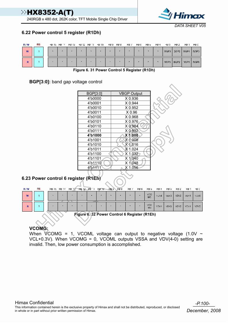
-P.100-Himax Confidential
December, 2008This information contained herein is the exclusive property of Himax and shall not be distributed, reproduced, or disclosed in whole or in part without prior written permission of Himax.
HX8352-A(T) 240RGB x 480 dot, 262K color, TFT Mobile Single Chip Driver
DATA SHEET V05
6.22 Power control 5 register (R1Dh)
Figure 6. 31 Power Control 5 Register (R1Dh)
BGP[3:0]: band gap voltage control
BGP[3:0] VBGP Output 4’b0000 X 0.936 4’b0001 X 0.944 4’b0010 X 0.952 4’b0011 X 0.96 4’b0100 X 0.968 4’b0101 X 0.976 4’b0110 X 0.984 4’b0111 X 0.992 4’b1000 X 1.000 4’b1001 X 1.008 4’b1010 X 1.016 4’b1011 X 1.024 4’b1100 X 1.032 4’b1101 X 1.040 4’b1110 X 1.048 4’b1111 X 1.056
6.23 Power control 6 register (R1Eh)
Figure 6. 32 Power Control 6 Register (R1Eh)
VCOMG: When VCOMG = 1, VCOML voltage can output to negative voltage (1.0V ~ VCL+0.3V). When VCOMG = 0, VCOML outputs VSSA and VDV(4-0) setting are invalid. Then, low power consumption is accomplished.
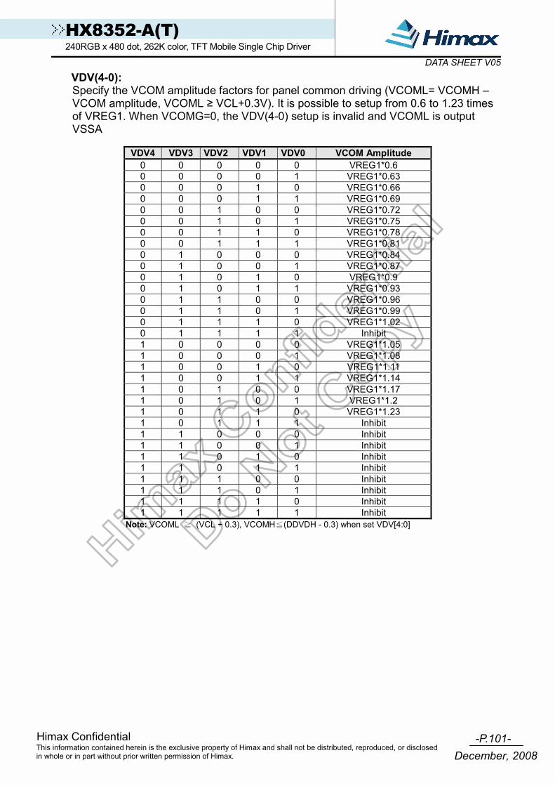
-P.101-Himax Confidential
December, 2008This information contained herein is the exclusive property of Himax and shall not be distributed, reproduced, or disclosed in whole or in part without prior written permission of Himax.
HX8352-A(T) 240RGB x 480 dot, 262K color, TFT Mobile Single Chip Driver
DATA SHEET V05
VDV(4-0): Specify the VCOM amplitude factors for panel common driving (VCOML= VCOMH – VCOM amplitude, VCOML ≥ VCL+0.3V). It is possible to setup from 0.6 to 1.23 times of VREG1. When VCOMG=0, the VDV(4-0) setup is invalid and VCOML is output VSSA
VDV4 VDV3 VDV2 VDV1 VDV0 VCOM Amplitude
0 0 0 0 0 VREG1*0.6 0 0 0 0 1 VREG1*0.63 0 0 0 1 0 VREG1*0.66 0 0 0 1 1 VREG1*0.69 0 0 1 0 0 VREG1*0.72 0 0 1 0 1 VREG1*0.75 0 0 1 1 0 VREG1*0.78 0 0 1 1 1 VREG1*0.81 0 1 0 0 0 VREG1*0.84 0 1 0 0 1 VREG1*0.87 0 1 0 1 0 VREG1*0.9 0 1 0 1 1 VREG1*0.93 0 1 1 0 0 VREG1*0.96 0 1 1 0 1 VREG1*0.99 0 1 1 1 0 VREG1*1.02 0 1 1 1 1 Inhibit 1 0 0 0 0 VREG1*1.05 1 0 0 0 1 VREG1*1.08 1 0 0 1 0 VREG1*1.11 1 0 0 1 1 VREG1*1.14 1 0 1 0 0 VREG1*1.17 1 0 1 0 1 VREG1*1.2 1 0 1 1 0 VREG1*1.23 1 0 1 1 1 Inhibit 1 1 0 0 0 Inhibit 1 1 0 0 1 Inhibit 1 1 0 1 0 Inhibit 1 1 0 1 1 Inhibit 1 1 1 0 0 Inhibit 1 1 1 0 1 Inhibit 1 1 1 1 0 Inhibit 1 1 1 1 1 Inhibit
Note: VCOML ≧ (VCL + 0.3), VCOMH≦(DDVDH - 0.3) when set VDV[4:0]

-P.102-Himax Confidential
December, 2008This information contained herein is the exclusive property of Himax and shall not be distributed, reproduced, or disclosed in whole or in part without prior written permission of Himax.
HX8352-A(T) 240RGB x 480 dot, 262K color, TFT Mobile Single Chip Driver
DATA SHEET V05
6.24 VCOM control register (R1Fh)
Figure 6. 33 VCOM Control Register (R1Fh)
VCM(6-0): Set the VCOMH voltage (High level voltage of VCOM) It is possible to amplify from 0.4 to 0.98 times of VREG1 voltage.
VCM6 VCM5 VCM4 VCM3 VCM2 VCM1 VCM0 VCOMH 0 0 0 0 0 0 0 VREG1 * 0.4 0 0 0 0 0 0 1 VREG1 * 0.405 0 0 0 0 0 1 0 VREG1 * 0.41 0 0 0 0 0 1 1 VREG1 * 0.415 0 0 0 0 1 0 0 VREG1 * 0.42 0 0 0 0 1 0 1 VREG1 * 0.425 0 0 0 0 1 1 0 VREG1 * 0.43 0 0 0 0 1 1 1 VREG1 * 0.435 0 0 0 1 0 0 0 VREG1 * 0.44 0 0 0 1 0 0 1 VREG1 * 0.445 0 0 0 1 0 1 0 VREG1 * 0.45 0 0 0 1 0 1 1 VREG1 * 0.455 0 0 0 1 1 0 0 VREG1 * 0.46 0 0 0 1 1 0 1 VREG1 * 0.465 0 0 0 1 1 1 0 VREG1 * 0.47 0 0 0 1 1 1 1 VREG1 * 0.475 0 0 1 0 0 0 0 VREG1 * 0.48 0 0 1 0 0 0 1 VREG1 * 0.485 0 0 1 0 0 1 0 VREG1 * 0.49 0 0 1 0 0 1 1 VREG1 * 0.495 0 0 1 0 1 0 0 VREG1 * 0.5 0 0 1 0 1 0 1 VREG1 * 0.505 0 0 1 0 1 1 0 VREG1 * 0.51 0 0 1 0 1 1 1 VREG1 * 0.515 0 0 1 1 0 0 0 VREG1 * 0.52 0 0 1 1 0 0 1 VREG1 * 0.525 0 0 1 1 0 1 0 VREG1 * 0.53 0 0 1 1 0 1 1 VREG1 * 0.535 0 0 1 1 1 0 0 VREG1 * 0.54 0 0 1 1 1 0 1 VREG1 * 0.545 0 0 1 1 1 1 0 VREG1 * 0.55 0 0 1 1 1 1 1 VREG1 * 0.555 0 1 0 0 0 0 0 VREG1 * 0.56 0 1 0 0 0 0 1 VREG1 * 0.565 0 1 0 0 0 1 0 VREG1 * 0.57 0 1 0 0 0 1 1 VREG1 * 0.575 0 1 0 0 1 0 0 VREG1 * 0.58 0 1 0 0 1 0 1 VREG1 * 0.585 0 1 0 0 1 1 0 VREG1 * 0.59 0 1 0 0 1 1 1 VREG1 * 0.595 0 1 0 1 0 0 0 VREG1 * 0.6 0 1 0 1 0 0 1 VREG1 * 0.605 0 1 0 1 0 1 0 VREG1 * 0.61 0 1 0 1 0 1 1 VREG1 * 0.615 0 1 0 1 1 0 0 VREG1 * 0.62 0 1 0 1 1 0 1 VREG1 * 0.625 0 1 0 1 1 1 0 VREG1 * 0.63 0 1 0 1 1 1 1 VREG1 * 0.635 0 1 1 0 0 0 0 VREG1 * 0.64 0 1 1 0 0 0 1 VREG1 * 0.645 0 1 1 0 0 1 0 VREG1 * 0.65 0 1 1 0 0 1 1 VREG1 * 0.655 0 1 1 0 1 0 0 VREG1 * 0.66 0 1 1 0 1 0 1 VREG1 * 0.665 0 1 1 0 1 1 0 VREG1 * 0.67 0 1 1 0 1 1 1 VREG1 * 0.675

-P.103-Himax Confidential
December, 2008This information contained herein is the exclusive property of Himax and shall not be distributed, reproduced, or disclosed in whole or in part without prior written permission of Himax.
HX8352-A(T) 240RGB x 480 dot, 262K color, TFT Mobile Single Chip Driver
DATA SHEET V05VCM6 VCM5 VCM4 VCM3 VCM2 VCM1 VCM0 VCOMH
0 1 1 1 0 0 0 VREG1 * 0.68 0 1 1 1 0 0 1 VREG1 * 0.685 0 1 1 1 0 1 0 VREG1 * 0.69 0 1 1 1 0 1 1 VREG1 * 0.695 0 1 1 1 1 0 0 VREG1 * 0.7 0 1 1 1 1 0 1 VREG1 * 0.705 0 1 1 1 1 1 0 VREG1 * 0.71
0 1 1 1 1 1 1 VCOMH can be adjusted from VCOMR with a external VR (variable resister),
1 0 0 0 0 0 0 VREG1 * 0.715 1 0 0 0 0 0 1 VREG1 * 0.72 1 0 0 0 0 1 0 VREG1 * 0.725 1 0 0 0 0 1 1 VREG1 * 0.73 1 0 0 0 1 0 0 VREG1 * 0.735 1 0 0 0 1 0 1 VREG1 * 0.74 1 0 0 0 1 1 0 VREG1 * 0.745 1 0 0 0 1 1 1 VREG1 * 0.75 1 0 0 1 0 0 0 VREG1 * 0.755 1 0 0 1 0 0 1 VREG1 * 0.76 1 0 0 1 0 1 0 VREG1 * 0.765 1 0 0 1 0 1 1 VREG1 * 0.77 1 0 0 1 1 0 0 VREG1 * 0.775 1 0 0 1 1 0 1 VREG1 * 0.78 1 0 0 1 1 1 0 VREG1 * 0.785 1 0 0 1 1 1 1 VREG1 * 0.79 1 0 1 0 0 0 0 VREG1 * 0.795 1 0 1 0 0 0 1 VREG1 * 0.8 1 0 1 0 0 1 0 VREG1 * 0.805 1 0 1 0 0 1 1 VREG1 * 0.81 1 0 1 0 1 0 0 VREG1 * 0.815 1 0 1 0 1 0 1 VREG1 * 0.82 1 0 1 0 1 1 0 VREG1 * 0.825 1 0 1 0 1 1 1 VREG1 * 0.83 1 0 1 1 0 0 0 VREG1 * 0.835 1 0 1 1 0 0 1 VREG1 * 0.84 1 0 1 1 0 1 0 VREG1 * 0.845 1 0 1 1 0 1 1 VREG1 * 0.85 1 0 1 1 1 0 0 VREG1 * 0.855 1 0 1 1 1 0 1 VREG1 * 0.86 1 0 1 1 1 1 0 VREG1 * 0.865 1 0 1 1 1 1 1 VREG1 * 0.87 1 1 0 0 0 0 0 VREG1 * 0.875 1 1 0 0 0 0 1 VREG1 * 0.88 1 1 0 0 0 1 0 VREG1 * 0.885 1 1 0 0 0 1 1 VREG1 * 0.89 1 1 0 0 1 0 0 VREG1 * 0.895 1 1 0 0 1 0 1 VREG1 * 0.9 1 1 0 0 1 1 0 VREG1 * 0.905 1 1 0 0 1 1 1 VREG1 * 0.91 1 1 0 1 0 0 0 VREG1 * 0.915 1 1 0 1 0 0 1 VREG1 * 0.92 1 1 0 1 0 1 0 VREG1 * 0.925 1 1 0 1 0 1 1 VREG1 * 0.93 1 1 0 1 1 0 0 VREG1 * 0.935 1 1 0 1 1 0 1 VREG1 * 0.94 1 1 0 1 1 1 0 VREG1 * 0.945 1 1 0 1 1 1 1 VREG1 * 0.95 1 1 1 0 0 0 0 VREG1 * 0.955 1 1 1 0 0 0 1 VREG1 * 0.96 1 1 1 0 0 1 0 VREG1 * 0.965 1 1 1 0 0 1 1 VREG1 * 0.97 1 1 1 0 1 0 0 VREG1 * 0.975 1 1 1 0 1 0 1 VREG1 * 0.98

-P.104-Himax Confidential
December, 2008This information contained herein is the exclusive property of Himax and shall not be distributed, reproduced, or disclosed in whole or in part without prior written permission of Himax.
HX8352-A(T) 240RGB x 480 dot, 262K color, TFT Mobile Single Chip Driver
DATA SHEET V05VCM6 VCM5 VCM4 VCM3 VCM2 VCM1 VCM0 VCOMH
1 1 1 0 1 1 0 inhibit 1 1 1 0 1 1 1 inhibit 1 1 1 1 0 0 0 inhibit 1 1 1 1 0 0 1 inhibit 1 1 1 1 0 1 0 inhibit 1 1 1 1 0 1 1 inhibit 1 1 1 1 1 0 0 inhibit 1 1 1 1 1 0 1 inhibit 1 1 1 1 1 1 0 inhibit
1 1 1 1 1 1 1 VCOMH can be adjusted from VCOMR with a external VR (variable resister)
6.25 Read data register (R22h)
R 1
R/W RS
RD17 RD16 RD15 RD14 RD13 RD12 RD11 RD10 RD9 RD8 RD7 RD6 RD5 RD4 RD3 RD2 RD1 RD0
RB15 RB14 RB13 RB12 RB11 RB10 RB9 RB8 RB7 RB6 RB5 RB4 RB3 RB2 RB1 RB0RB17 RB16
Figure 6. 34 Read Data Register (R22h)
RD17-0: Read 18-bit data from GRAM through the read data register (RDR). When the data is read by microcomputer, the first-word read immediately after the GRAM address setting is latched from the GRAM to the internal read-data latch. The data on the data bus (D17–0) becomes invalid and the second-word read is normal. Write data register (R22h)
W 1
R/W RS
WD15 WD14 WD13 WD12 WD11 WD10 WD9 WD8 WD7 WD6 WD5 WD4 WD3 WD2 WD1 WD0
RB15 RB14 RB13 RB12 RB11 RB10 RB9 RB8 RB7 RB6 RB5 RB4 RB3 RB2 RB1 RB0
Figure 6. 35 Write Data Register (R22h)
WD[15:0]: Transforms the data into 16-bit bus before written to GRAM through the write data register (WDR). After a write operation is issued, the address is automatically updated according to the MV, MX and MY bits. Note: When IC received R22h, then HX8352-A didn’t re-set to start address. If start address want re-set again, then
SC (R02h~R03h) and SP (R06h~R07h) register need to re-set again.

-P.105-Himax Confidential
December, 2008This information contained herein is the exclusive property of Himax and shall not be distributed, reproduced, or disclosed in whole or in part without prior written permission of Himax.
HX8352-A(T) 240RGB x 480 dot, 262K color, TFT Mobile Single Chip Driver
DATA SHEET V05
6.26 Display control 1 register (R23h)
Figure 6. 36 Display Control Register (R23h)
TEMODE: Specify the Tearing-Effect mode. When TEMODE=0: The Tearing Effect Output line consists of V-Blanking information only.
When TEMODE =1: The Tearing Effect Output Line consists of both V-Blanking and H-Blanking information
Note: During Sleep in Mode with Tearing Effect Line On, Tearing Effect Output pin active low
TEON: This command is used to turn ON the Tearing Effect output signal from the TE signal line. This output is not affected by changing Memory Access Control bit B4.
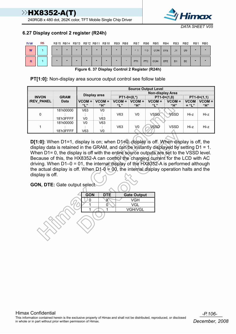
-P.106-Himax Confidential
December, 2008This information contained herein is the exclusive property of Himax and shall not be distributed, reproduced, or disclosed in whole or in part without prior written permission of Himax.
HX8352-A(T) 240RGB x 480 dot, 262K color, TFT Mobile Single Chip Driver
DATA SHEET V05
6.27 Display control 2 register (R24h)
Figure 6. 37 Display Control 2 Register (R24h)
PT[1:0]: Non-display area source output control see follow table
Source Output Level
Non-display Area Display area PT1-0=(0,*) PT1-0=(1,0) PT1-0=(1,1) INVON /REV_PANEL
GRAM Data VCOM =
“L” VCOM =
“H” VCOM =
“L” VCOM =
“H” VCOM =
“L” VCOM =
“H” VCOM = “L”
VCOM = “H”
0 18’h00000
: 18’h3FFFF
V63 :
V0
V0 :
V63 V63 V0 VSSD VSSD Hi-z Hi-z
1 18’h00000
: 18’h3FFFF
V0 :
V63
V63 :
V0 V63 V0 VSSD VSSD Hi-z Hi-z
D[1:0]: When D1=1, display is on; when D1=0, display is off. When display is off, the display data is retained in the GRAM, and can be instantly displayed by setting D1 = 1. When D1= 0, the display is off with the entire source outputs are set to the VSSD level. Because of this, the HX8352-A can control the charging current for the LCD with AC driving. When D1–0 = 01, the internal display of the HX8352-A is performed although the actual display is off. When D1-0 = 00, the internal display operation halts and the display is off.
GON, DTE: Gate output select.
GON DTE Gate Output
0 X VGH 1 0 VGL 1 1 VGH/VGL
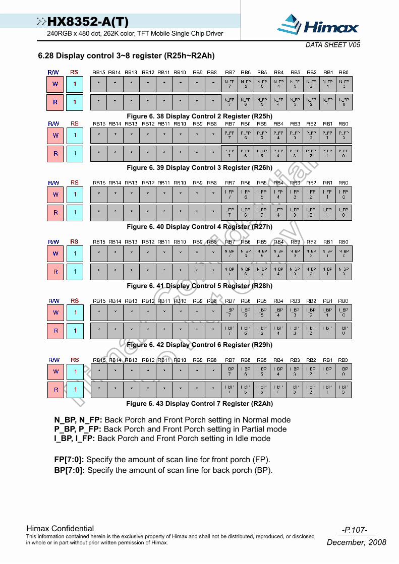
-P.107-Himax Confidential
December, 2008This information contained herein is the exclusive property of Himax and shall not be distributed, reproduced, or disclosed in whole or in part without prior written permission of Himax.
HX8352-A(T) 240RGB x 480 dot, 262K color, TFT Mobile Single Chip Driver
DATA SHEET V05
6.28 Display control 3~8 register (R25h~R2Ah)
Figure 6. 38 Display Control 2 Register (R25h)
Figure 6. 39 Display Control 3 Register (R26h)
Figure 6. 40 Display Control 4 Register (R27h)
Figure 6. 41 Display Control 5 Register (R28h)
Figure 6. 42 Display Control 6 Register (R29h)
Figure 6. 43 Display Control 7 Register (R2Ah)
N_BP, N_FP: Back Porch and Front Porch setting in Normal mode P_BP, P_FP: Back Porch and Front Porch setting in Partial mode
I_BP, I_FP: Back Porch and Front Porch setting in Idle mode FP[7:0]: Specify the amount of scan line for front porch (FP). BP[7:0]: Specify the amount of scan line for back porch (BP).
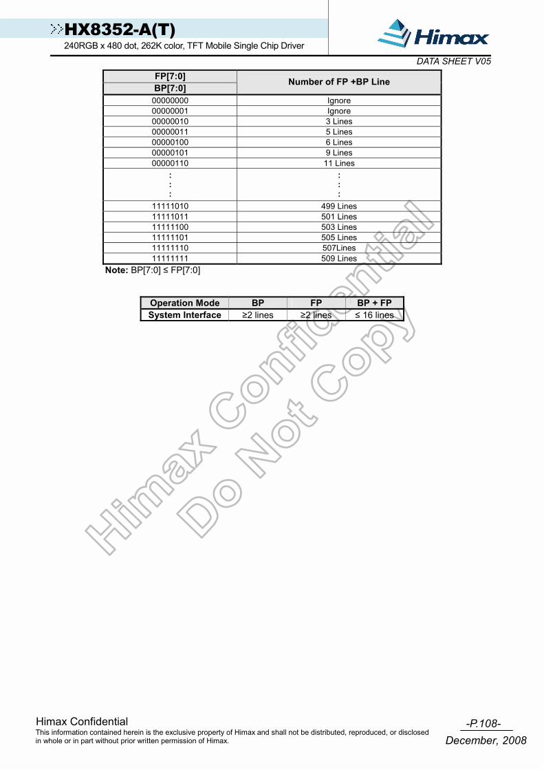
-P.108-Himax Confidential
December, 2008This information contained herein is the exclusive property of Himax and shall not be distributed, reproduced, or disclosed in whole or in part without prior written permission of Himax.
HX8352-A(T) 240RGB x 480 dot, 262K color, TFT Mobile Single Chip Driver
DATA SHEET V05FP[7:0] BP[7:0]
Number of FP +BP Line
00000000 Ignore 00000001 Ignore 00000010 3 Lines 00000011 5 Lines 00000100 6 Lines 00000101 9 Lines 00000110 11 Lines
: : :
: : :
11111010 499 Lines 11111011 501 Lines 11111100 503 Lines 11111101 505 Lines 11111110 507Lines 11111111 509 Lines
Note: BP[7:0] ≤ FP[7:0]
Operation Mode BP FP BP + FP System Interface ≥2 lines ≥2 lines ≤ 16 lines

-P.109-Himax Confidential
December, 2008This information contained herein is the exclusive property of Himax and shall not be distributed, reproduced, or disclosed in whole or in part without prior written permission of Himax.
HX8352-A(T) 240RGB x 480 dot, 262K color, TFT Mobile Single Chip Driver
DATA SHEET V05
6.29 Cycle control 1~3 register (R2B~2Dh)
Figure 6. 44 Cycle Control 1 Register (R2Bh)
Figure 6. 45 Cycle Control 2 Register (R2Ch)
Figure 6. 46 Cycle Control 3 Register (R2Dh)
N_DC: Normal mode P_DC: Partial mode I_DC: Idle mode DC(7-0): specify the clock frequency for DC/DC converter operating.
fosc= R-C oscillation frequency
DC7 DC6 DC5 DC4 DC3 DC2 DC1 DC0 DCDCf 0 0 0 0 0 0 0 0 Inhibited 0 0 0 0 0 0 0 1 fosc 0 0 0 0 0 0 1 0 fosc/ 2
: : 1 1 1 1 1 1 1 0 fosc/ 254 1 1 1 1 1 1 1 1 fosc / 255
Note: It is recommended to set DC(7-0) as “20”h, which means one charge bump clock periodis 32 internal oscillation clocks.

-P.110-Himax Confidential
December, 2008This information contained herein is the exclusive property of Himax and shall not be distributed, reproduced, or disclosed in whole or in part without prior written permission of Himax.
HX8352-A(T) 240RGB x 480 dot, 262K color, TFT Mobile Single Chip Driver
DATA SHEET V05
6.30 Cycle control 4~8 register (R2E~32h)
Figure 6. 47 Cycle Control 4 Register (R2Eh)
Figure 6. 48 Cycle Control 5 Register (R2Fh)
Figure 6. 49 Cycle Control 1 Register (R30h)
Figure 6. 50 Cycle Control 2 Register (R31h)
Figure 6. 51 Cycle Control 3 Register (R32h)
FS0(1-0): Set the operating frequency of the step-up circuit 1 and extra step-up circuit 1 for VLCD voltage generation. When using the higher frequency, the driving ability of the step-up circuit and the display quality are high, but the current consumption is increased. The tradeoff is between the display quality and the current consumption.
DCDCf = DC / DC converter operating frequency
FS01 FS0 Operation Frequency of Step-up Circuit 1 and Extra Step-up circuit 1
0 0 DCDCf / 1 0 1 DCDCf / 2 1 0 DCDCf / 4 1 1 DCDCf / 8
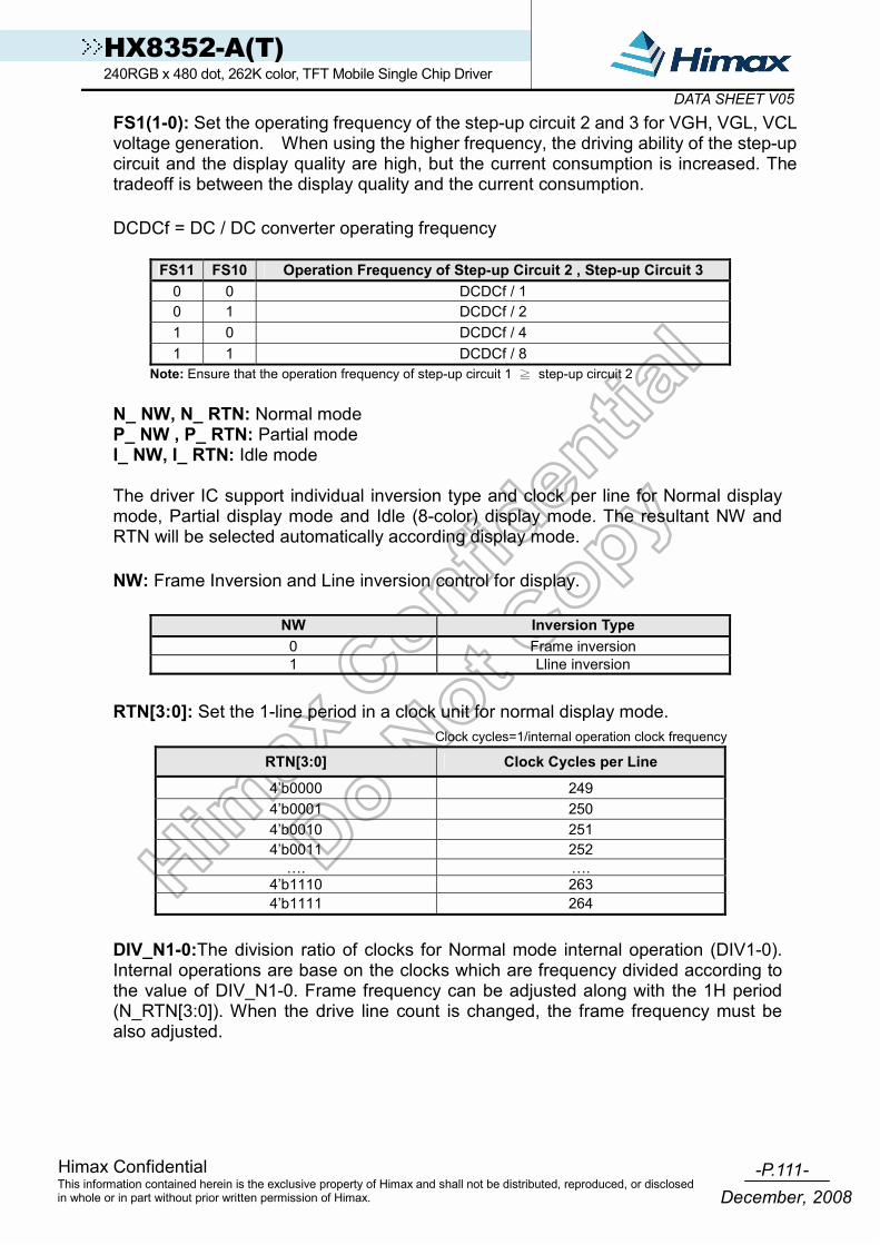
-P.111-Himax Confidential
December, 2008This information contained herein is the exclusive property of Himax and shall not be distributed, reproduced, or disclosed in whole or in part without prior written permission of Himax.
HX8352-A(T) 240RGB x 480 dot, 262K color, TFT Mobile Single Chip Driver
DATA SHEET V05
FS1(1-0): Set the operating frequency of the step-up circuit 2 and 3 for VGH, VGL, VCL voltage generation. When using the higher frequency, the driving ability of the step-up circuit and the display quality are high, but the current consumption is increased. The tradeoff is between the display quality and the current consumption.
DCDCf = DC / DC converter operating frequency
FS11 FS10 Operation Frequency of Step-up Circuit 2 , Step-up Circuit 3 0 0 DCDCf / 1 0 1 DCDCf / 2 1 0 DCDCf / 4 1 1 DCDCf / 8
Note: Ensure that the operation frequency of step-up circuit 1 ≧ step-up circuit 2 N_ NW, N_ RTN: Normal mode P_ NW , P_ RTN: Partial mode I_ NW, I_ RTN: Idle mode The driver IC support individual inversion type and clock per line for Normal display mode, Partial display mode and Idle (8-color) display mode. The resultant NW and RTN will be selected automatically according display mode. NW: Frame Inversion and Line inversion control for display.
NW Inversion Type 0 Frame inversion 1 Lline inversion
RTN[3:0]: Set the 1-line period in a clock unit for normal display mode. Clock cycles=1/internal operation clock frequency
RTN[3:0] Clock Cycles per Line
4’b0000 249 4’b0001 250 4’b0010 251 4’b0011 252
…. ….4’b1110 2634’b1111 264
DIV_N1-0:The division ratio of clocks for Normal mode internal operation (DIV1-0). Internal operations are base on the clocks which are frequency divided according to the value of DIV_N1-0. Frame frequency can be adjusted along with the 1H period (N_RTN[3:0]). When the drive line count is changed, the frame frequency must be also adjusted.
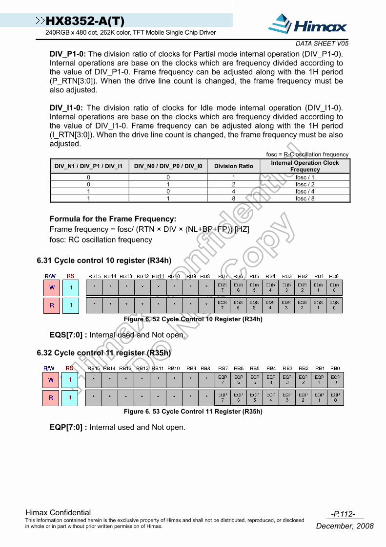
-P.112-Himax Confidential
December, 2008This information contained herein is the exclusive property of Himax and shall not be distributed, reproduced, or disclosed in whole or in part without prior written permission of Himax.
HX8352-A(T) 240RGB x 480 dot, 262K color, TFT Mobile Single Chip Driver
DATA SHEET V05
DIV_P1-0: The division ratio of clocks for Partial mode internal operation (DIV_P1-0). Internal operations are base on the clocks which are frequency divided according to the value of DIV_P1-0. Frame frequency can be adjusted along with the 1H period (P_RTN[3:0]). When the drive line count is changed, the frame frequency must be also adjusted. DIV_I1-0: The division ratio of clocks for Idle mode internal operation (DIV_I1-0). Internal operations are base on the clocks which are frequency divided according to the value of DIV_I1-0. Frame frequency can be adjusted along with the 1H period (I_RTN[3:0]). When the drive line count is changed, the frame frequency must be also adjusted.
fosc = R-C oscillation frequency
DIV_N1 / DIV_P1 / DIV_I1 DIV_N0 / DIV_P0 / DIV_I0 Division Ratio Internal Operation Clock Frequency
0 0 1 fosc / 1 0 1 2 fosc / 2 1 0 4 fosc / 4 1 1 8 fosc / 8
Formula for the Frame Frequency: Frame frequency = fosc/ (RTN × DIV × (NL+BP+FP)) [HZ] fosc: RC oscillation frequency
6.31 Cycle control 10 register (R34h)
Figure 6. 52 Cycle Control 10 Register (R34h)
EQS[7:0] : Internal used and Not open.
6.32 Cycle control 11 register (R35h)
Figure 6. 53 Cycle Control 11 Register (R35h)
EQP[7:0] : Internal used and Not open.
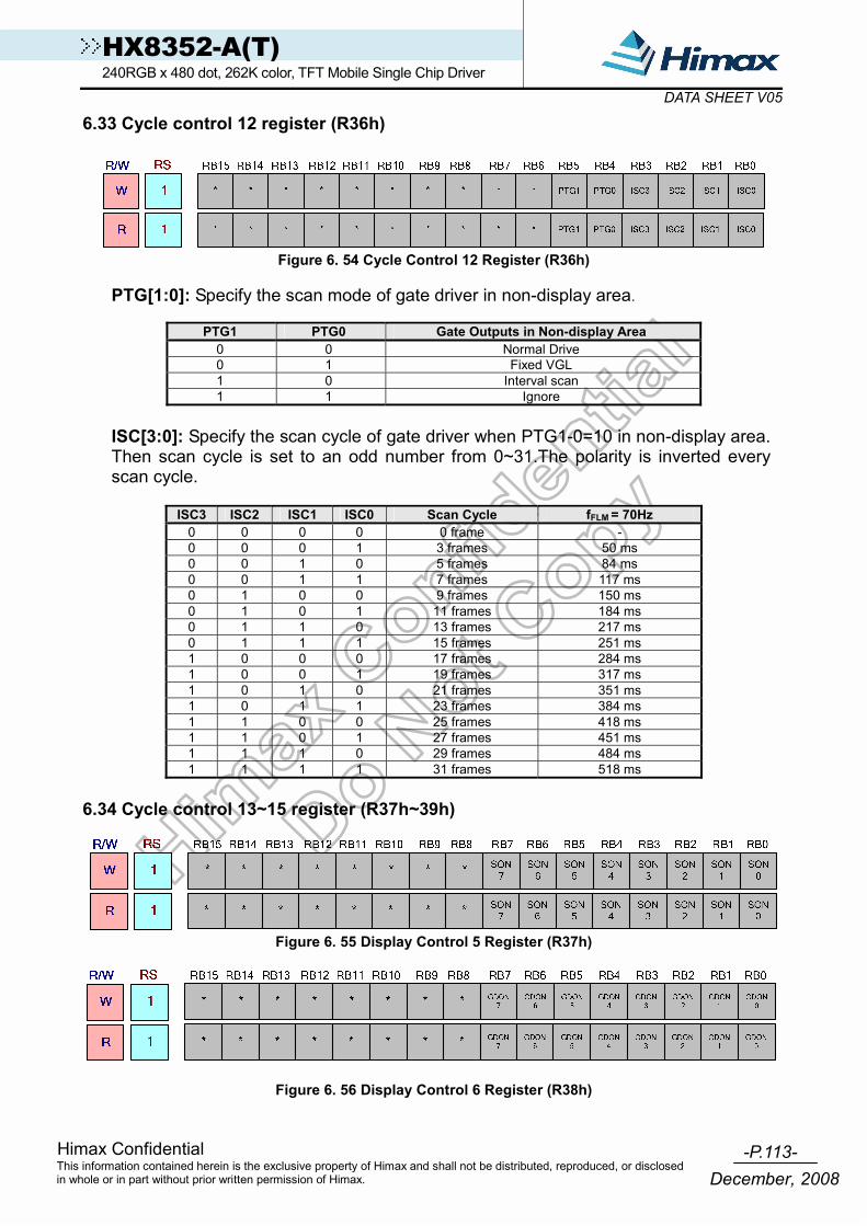
-P.113-Himax Confidential
December, 2008This information contained herein is the exclusive property of Himax and shall not be distributed, reproduced, or disclosed in whole or in part without prior written permission of Himax.
HX8352-A(T) 240RGB x 480 dot, 262K color, TFT Mobile Single Chip Driver
DATA SHEET V05
6.33 Cycle control 12 register (R36h)
Figure 6. 54 Cycle Control 12 Register (R36h)
PTG[1:0]: Specify the scan mode of gate driver in non-display area.
PTG1 PTG0 Gate Outputs in Non-display Area
0 0 Normal Drive 0 1 Fixed VGL 1 0 Interval scan 1 1 Ignore
ISC[3:0]: Specify the scan cycle of gate driver when PTG1-0=10 in non-display area. Then scan cycle is set to an odd number from 0~31.The polarity is inverted every scan cycle.
ISC3 ISC2 ISC1 ISC0 Scan Cycle fFLM = 70Hz
0 0 0 0 0 frame - 0 0 0 1 3 frames 50 ms 0 0 1 0 5 frames 84 ms 0 0 1 1 7 frames 117 ms 0 1 0 0 9 frames 150 ms 0 1 0 1 11 frames 184 ms 0 1 1 0 13 frames 217 ms 0 1 1 1 15 frames 251 ms 1 0 0 0 17 frames 284 ms 1 0 0 1 19 frames 317 ms 1 0 1 0 21 frames 351 ms 1 0 1 1 23 frames 384 ms 1 1 0 0 25 frames 418 ms 1 1 0 1 27 frames 451 ms 1 1 1 0 29 frames 484 ms 1 1 1 1 31 frames 518 ms
6.34 Cycle control 13~15 register (R37h~39h)
Figure 6. 55 Display Control 5 Register (R37h)
Figure 6. 56 Display Control 6 Register (R38h)

-P.114-Himax Confidential
December, 2008This information contained herein is the exclusive property of Himax and shall not be distributed, reproduced, or disclosed in whole or in part without prior written permission of Himax.
HX8352-A(T) 240RGB x 480 dot, 262K color, TFT Mobile Single Chip Driver
DATA SHEET V05
Figure 6. 57 Display Control 3 Register (R39h)
The HX8352-A can control the display operation period time for LCD panel driving as follow:
1-Line Period
SON
GDONGDOF
Source Output Period
Gate Output Period
Nth Gate Output Period
N+1th Gate Output Period
S1 - S720
G(N)
G(N+1)
Hi-zHi-z
SON7-0: Specify the valid source output start time in 1-line driving period. The period time is defined as SYSCLK clock number. (Please note that the setting “00h” and “01h” is inhibited).
GDON7-0: Specify the valid gate output start time in 1-line driving period. The period time is defined as SYSCLK clock number in internal clock display mode. The period time is defined as setting value x 8 DOTCLK clock number in external clock display mode. (Please note that the setting “00h”, “01h”, “02h” is inhibited).
GDOF7-0: Specify the gate output end time in 1-line driving period. The period time is defined as SYSCLK clock number in internal clock display mode. The period time is defined as setting value x 8 DOTCLK clock number in external clock display mode. (Please note that the GDOF7-0 ≤ HCK-1).
6.35 Interface control 1 register (R3Ah)
Figure 6. 58 Interface Control 1 Register (R3Ah)

-P.115-Himax Confidential
December, 2008This information contained herein is the exclusive property of Himax and shall not be distributed, reproduced, or disclosed in whole or in part without prior written permission of Himax.
HX8352-A(T) 240RGB x 480 dot, 262K color, TFT Mobile Single Chip Driver
DATA SHEET V05
This command is used to set RGB interface and Serial bus interface related register CSEL: RGB interface data format select.
Interface Format CSEL2 CSEL1 CSEL0 Not Defined 0 0 0 Not Defined 0 0 1 Not Defined 0 1 0 Not Defined 0 1 1 Not Defined 1 0 0 16 Bit/Pixel 1 0 1 18 Bit/Pixel 1 1 0 Not Defined 1 1 1
EPL: Specify the polarity of Enable pin in RGB interface mode. EPL=0, the Enable is High active; EPL=1, the Enable is Low active VSPL: The polarity of VSYNC pin. When VSPL=0, the VSYNC pin is Low active. When VSPL=1, the VSYNC pin is High active. HSPL: The polarity of HSYNC pin. When HSPL=0, the HSYNC pin is Low active. When HSPL=1, the HSYNC pin is High active. DPL: The polarity of DOTCLK pin. When DPL=0, the data is read on the rising edge of DOTCLK signal. When DPL=1, the data is read on the falling edge of DOTCLK signal.
6.36 Source control 1~2 register (R3Ch~3Dh)
Figure 6. 59 Source Control 1 Register (R3Ch)
Figure 6. 60 Source Control 2 Register (R3Dh)
N_SAP[7:0]: Normal mode I_SAP[7:0]: Idle mode SAP[7:0]: Adjust the amount of fixed current from the fixed current source for the operational amplifier in the source driver. When the amount of fixed current is increased, the LCD driving capacity and the display quality are high, but the current consumption is increased. The tradeoff is between display quality and current consumption. During no display operation, when SAP[7–0] = 0x00h, the current consumption can be reduced by stopping the operational amplifier.

-P.116-Himax Confidential
December, 2008This information contained herein is the exclusive property of Himax and shall not be distributed, reproduced, or disclosed in whole or in part without prior written permission of Himax.
HX8352-A(T) 240RGB x 480 dot, 262K color, TFT Mobile Single Chip Driver
DATA SHEET V05
N_SAP[7:0] / I_SAP[7:0] Source driving ability Turn Off time 0 0 0 0 0 0 0 0 Source output all stop 0 0 0 0 0 0 0 1 1- clock 0 0 0 0 0 0 1 0 2- clock 0 0 0 0 0 0 1 1 3- clock 0 0 0 0 0 1 0 0 4- clock 0 0 0 0 0 1 0 1 5- clock 0 0 0 0 0 1 1 0 6- clock 0 0 0 0 0 1 1 1 7- clock - - -
- - -
- - -
- - -
- - -
- - -
- - -
- - -
1 1 1 1 1 0 0 1 249- clock 1 1 1 1 1 0 1 0 250- clock 1 1 1 1 1 0 1 1 251- clock 1 1 1 1 1 1 0 0 252- clock 1 1 1 1 1 1 0 1 253- clock 1 1 1 1 1 1 1 0 254- clock 1 1 1 1 1 1 1 1 255- clock
6.37 GAMMA control 1~12 register (R3E~49h)
Figure 6. 61 GAMMA Control 1 Register (R3Eh)
Figure 6. 62 GAMMA Control 2 Register (R3Fh)
Figure 6. 63 GAMMA Control 3 Register (R40h)
Figure 6. 64 GAMMA Control 4 Register (R41h)
Figure 6. 65 GAMMA Control 5 Register (R42h)

-P.117-Himax Confidential
December, 2008This information contained herein is the exclusive property of Himax and shall not be distributed, reproduced, or disclosed in whole or in part without prior written permission of Himax.
HX8352-A(T) 240RGB x 480 dot, 262K color, TFT Mobile Single Chip Driver
DATA SHEET V05
Figure 6. 66 GAMMA Control 6 Register (R43h)
Figure 6. 67 GAMMA Control 7 Register (R44h)
Figure 6. 68 GAMMA Control8 Register (R45h)
RB15 RB14 RB13 RB12 RB11 RB10 RB9 RB8 RB7 RB6 RB5 RB4 RB3 RB2 RB1 RB0
* * * * * * * * CGMP11
CGMP10
CGMP01
CGMP00 OP03 OP01 OP00
* * * * * * * *
OP02
CGMP11
CGMP10
CGMP01
OP03 OP01 OP00OP02CGMP
00
Figure 6. 69 GAMMA Control 9 Register (R46h)
Figure 6. 70 GAMMA Control 10 Register (R47h)
Figure 6. 71 GAMMA Control 11 Register (R48h)
Figure 6. 72 GAMMA Control 12 Register (R49h)

-P.118-Himax Confidential
December, 2008This information contained herein is the exclusive property of Himax and shall not be distributed, reproduced, or disclosed in whole or in part without prior written permission of Himax.
HX8352-A(T) 240RGB x 480 dot, 262K color, TFT Mobile Single Chip Driver
DATA SHEET V05
CP1-0 [2:0]: Gamma Center Adjustment registers for positive polarity output CN1-0 [2:0]: Gamma Center Adjustment registers for negative polarity output NP5-0 [2:0]: Gamma Macro Adjustment registers for positive polarity output NN5-0 [2:0]: Gamma Macro Adjustment registers for negative polarity output OP0 [3:0]/OP1 [4:0]: Gamma Offset Adjustment register for positive polarity output ON0 [3:0]/ON1 [4:0]: Gamma Offset Adjustment register for negative polarity output CGMP0[1:0], CGMP1[1:0]: Gamma Tap Adjustment register for positive polarity output CGMN0[1:0], CGMN1[1:0]: Gamma Tap Adjustment register for negative polarity output CGMP2, CGMP3: Gamma Harmony adjustment registers for positive polarity output CGMN2, CGMN3: Gamma Harmony adjustment registers for negative polarity output GSEL: V0, V256 reference voltage selection. GSEL=1, V0=VgP/N0, V63= VgP/N7; If GSEL=0, V0=VREG1, V63= VGS. For details, please refer to 5.9.4 Gamma resister stream and 8 to 1 Selector.
This command is used to set Gamma Curve Related Setting
Register Groups
Positive Polarity
Negative Polarity Description
CP0 2-0 CN0 2-0 Variable resistor (VRCP/N0) for center adjustment Center Adjustment CP1 2-0 CN1 2-0 Variable resistor (VRCP/N1)for center adjustment
NP0 2-0 NN0 2-0 8-to-1 selector (voltage level of grayscale 1) NP1 2-0 NN1 2-0 8-to-1 selector (voltage level of grayscale 8) NP2 2-0 NN2 2-0 8-to-1 selector (voltage level of grayscale 20) NP3 2-0 NN3 2-0 8-to-1 selector (voltage level of grayscale 43) NP4 2-0 NN4 2-0 8-to-1 selector (voltage level of grayscale 55)
Macro Adjustment
NP5 2-0 NN5 2-0 8-to-1 selector (voltage level of grayscale 62) OP0 3-0 ON0 3-0 Variable resistor (VROP/N0)for offset adjustment Offset
Adjustment OP1 4-0 ON1 4-0 Variable resistor (VROP/N1)for offset adjustment
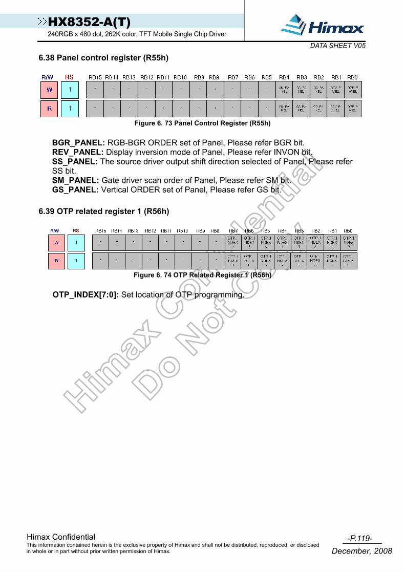
-P.119-Himax Confidential
December, 2008This information contained herein is the exclusive property of Himax and shall not be distributed, reproduced, or disclosed in whole or in part without prior written permission of Himax.
HX8352-A(T) 240RGB x 480 dot, 262K color, TFT Mobile Single Chip Driver
DATA SHEET V05
6.38 Panel control register (R55h)
Figure 6. 73 Panel Control Register (R55h)
BGR_PANEL: RGB-BGR ORDER set of Panel, Please refer BGR bit. REV_PANEL: Display inversion mode of Panel, Please refer INVON bit. SS_PANEL: The source driver output shift direction selected of Panel, Please refer SS bit. SM_PANEL: Gate driver scan order of Panel, Please refer SM bit. GS_PANEL: Vertical ORDER set of Panel, Please refer GS bit.
6.39 OTP related register 1 (R56h)
Figure 6. 74 OTP Related Register 1 (R56h)
OTP_INDEX[7:0]: Set location of OTP programming.
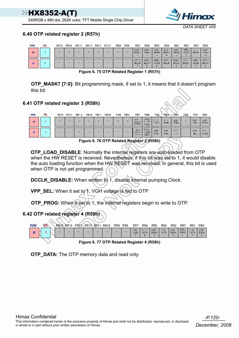
-P.120-Himax Confidential
December, 2008This information contained herein is the exclusive property of Himax and shall not be distributed, reproduced, or disclosed in whole or in part without prior written permission of Himax.
HX8352-A(T) 240RGB x 480 dot, 262K color, TFT Mobile Single Chip Driver
DATA SHEET V05
6.40 OTP related register 2 (R57h)
Figure 6. 75 OTP Related Register 1 (R57h)
OTP_MASK7 [7:0]: Bit programming mask, if set to 1, it means that it doesn’t program this bit
6.41 OTP related register 3 (R58h)
Figure 6. 76 OTP Related Register 3 (R58h)
OTP_LOAD_DISABLE: Normally the internal registers are auto-loaded from OTP when the HW RESET is received. Nevertheless, if this bit was set to 1, it would disable the auto loading function when the HW RESET was received. In general, this bit is used when OTP is not yet programmed. DCCLK_DISABLE: When written to 1, disable internal pumping Clock. VPP_SEL: When it set to 1, VGH voltage is fed to OTP OTP_PROG: When it set to 1, the internal registers begin to write to OTP.
6.42 OTP related register 4 (R59h)
Figure 6. 77 OTP Related Register 4 (R59h)
OTP_DATA: The OTP memory data and read only.
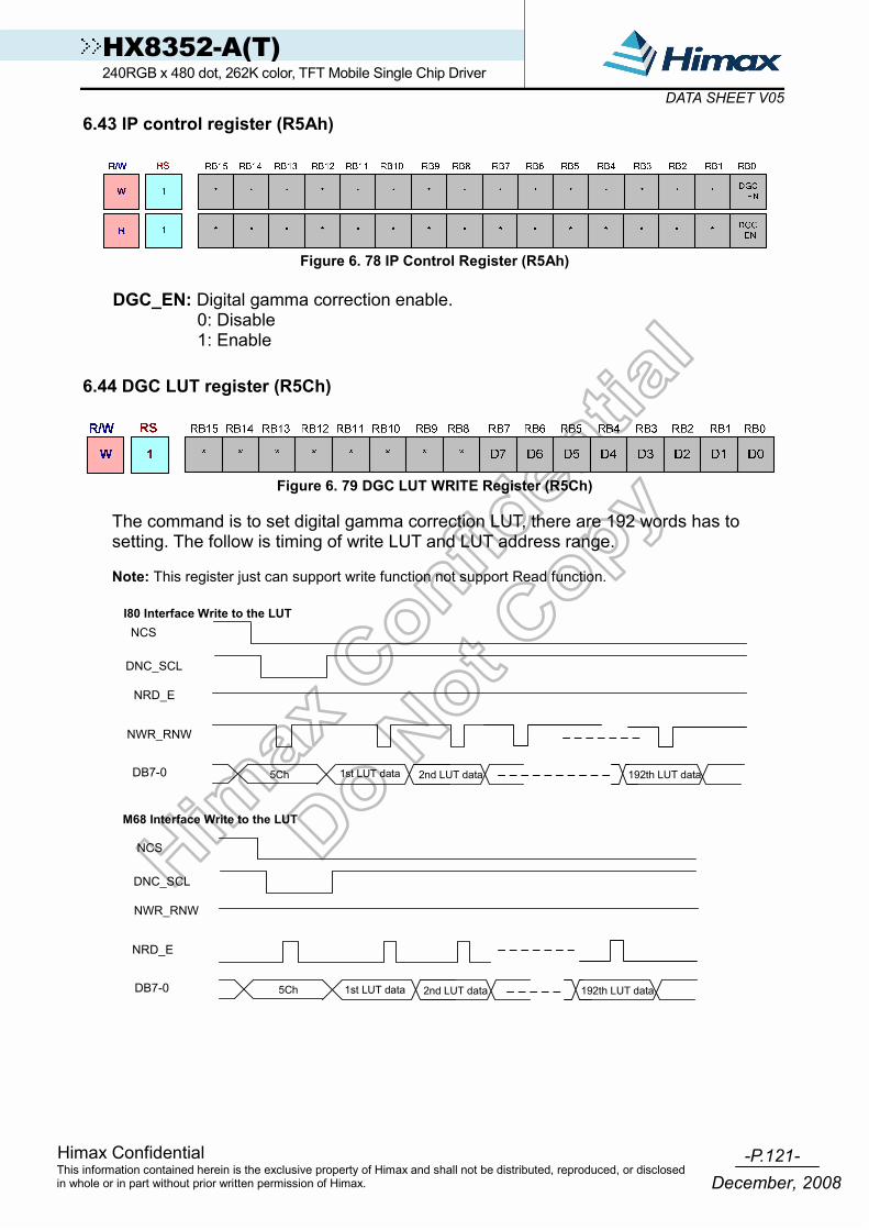
-P.121-Himax Confidential
December, 2008This information contained herein is the exclusive property of Himax and shall not be distributed, reproduced, or disclosed in whole or in part without prior written permission of Himax.
HX8352-A(T) 240RGB x 480 dot, 262K color, TFT Mobile Single Chip Driver
DATA SHEET V05
6.43 IP control register (R5Ah)
Figure 6. 78 IP Control Register (R5Ah)
DGC_EN: Digital gamma correction enable.
0: Disable 1: Enable
6.44 DGC LUT register (R5Ch)
Figure 6. 79 DGC LUT WRITE Register (R5Ch)
The command is to set digital gamma correction LUT, there are 192 words has to setting. The follow is timing of write LUT and LUT address range. Note: This register just can support write function not support Read function.
I80 Interface Write to the LUT
NCS
DNC_SCL
NWR_RNW
M68 Interface Write to the LUT
1st LUT dataDB7-0
NRD_E
5Ch
2nd LUT data 192th LUT data
NCS
DNC_SCL
NRD_E
1st LUT data DB7-0
NWR_RNW
5Ch
192th LUT data2nd LUT data

-P.122-Himax Confidential
December, 2008This information contained herein is the exclusive property of Himax and shall not be distributed, reproduced, or disclosed in whole or in part without prior written permission of Himax.
HX8352-A(T) 240RGB x 480 dot, 262K color, TFT Mobile Single Chip Driver
DATA SHEET V05
LUT D7 D6 D5 D4 D3 D2 D1 D01st R007 R006 R005 R004 R003 R002 R001 R000
2nd R017 R016 R015 R014 R013 R012 R011 R010
: :
: :
: :
: :
: :
: :
: :
: :
: :
63 R627 R626 R625 R624 R623 R622 R621 R620
64 R637 R636 R635 R634 R633 R632 R631 R630
65 G007 G006 G005 G004 G003 G002 G001 G000
66 G017 G016 G015 G014 G013 G012 G011 G010
: :
: :
: :
: :
: :
: :
: :
: :
: :
127 G627 G626 G625 G624 G623 G622 G621 G620
128 G637 G636 G635 G634 G633 G632 G631 G630
129 B007 B006 B005 B004 B003 B002 B001 B000
130 B017 B016 B015 B014 B013 B012 B011 B010
: :
: :
: :
: :
: :
: :
: :
: :
: :
101 B627 B626 B625 B624 B623 B622 B621 B620
192 B637 B636 B635 B634 B633 B632 B631 B630
6.45 Test mode control register (R83h)
Figure 6. 80 TEST MODE Control Register (R83h)
When TEST_MODE=1, then in-housedregister can updated new setting.
6.46 VDDD control register (R85h)
Figure 6. 81 VDDD Control Register (R85h) VDC_SEL(2-0): VDDD will increase or reduce by VDC_SEL setting.

-P.123-Himax Confidential
December, 2008This information contained herein is the exclusive property of Himax and shall not be distributed, reproduced, or disclosed in whole or in part without prior written permission of Himax.
HX8352-A(T) 240RGB x 480 dot, 262K color, TFT Mobile Single Chip Driver
DATA SHEET V05
6.47 Power driving control register (R8Ah)
RB15 RB14 RB13 RB12 RB11 RB10 RB9 RB8 RB7 RB6 RB5 RB4 RB3 RB2 RB1 RB0
* * * * * * * * 0 0 0 0 0 PTBA1 PTBA0
* * * * * * * *
PTBA2
0 0 0 0 0 PTBA1 PTBA0PTBA2
Figure 6. 82 Power driving control register (R8Ah)
Resistor Setting Power driving ability PTBA[2:0] AP[1:0]=01/10/11
000 0.00Iref 001 0.17Iref 010 0.33Iref 011 0.50Iref 100 0.67Iref 101 0.83Iref 110 1.00Iref 111 1.17Iref
6.48 Source gamma resistor setting register (R8B~R8Ch)
Figure 6. 83 Source Gamma resistor setting 1 Register (R8Bh)
Figure 6. 84 Source Gamma resistor setting 2 Register (R8Ch)
Resistor Setting GS_RES0 GS_RES1
Resistor
0 X 0 ohm 1 0 120K ohm 1 1 60K ohm

-P.124-Himax Confidential
December, 2008This information contained herein is the exclusive property of Himax and shall not be distributed, reproduced, or disclosed in whole or in part without prior written permission of Himax.
HX8352-A(T) 240RGB x 480 dot, 262K color, TFT Mobile Single Chip Driver
DATA SHEET V05
6.49 SYNC function register (R91h)
Figure 6. 85 SYNC Function Register (R91h)
DCDCLK_SYNC: Control synchronous function between DCDC_CLK and Display CLK.
DCDCLK_SYC=1, function Enable. DCDCLK_SYC=0, function Disable.
6.50 PWM control 1 register (R95h)
Figure 6. 86 PWM Control 1 Register (R95h)
DBV[7:0] Duty Cycle
0 1/255 1 2/255 2 3/255 3 4/255 : :
: :
252 252/255 253 253/255 254 254/255 255 255/255
Note: If BCTRL=0, then DBV[7:0]=0x00h.
6.50 PWM control 2 register (R96h)
Figure 6. 87 PWM Control 2 Register (R96h)
BL=1, Backlight control circuit turn on. BCTRL=0, the DBV[7:0]=0x00h. BCTRL=1, the DBV[7:0] can be active. Note: The frequency of PWM is 300Hz.

-P.125-Himax Confidential
December, 2008This information contained herein is the exclusive property of Himax and shall not be distributed, reproduced, or disclosed in whole or in part without prior written permission of Himax.
HX8352-A(T) 240RGB x 480 dot, 262K color, TFT Mobile Single Chip Driver
DATA SHEET V05
6.51 PWM control 3 register (R97h)
Figure 6. 88 PWM Control 2 Register (R96h)
C[1:0] CABC Mode Note
00 CABC Off/ Mannual Mode - 01 UI Mode The display pattern is belong pattern of Text 10 Still Mode The display is belong pattern of true color 11 Moving Mode The patter nis belong pattern of Moving
6.52 CABC PWM period control 1 Register (R6Bh)
Figure 6. 89 CABC PWM Period control 1 Register (R6Bh)
SEL_PWMCLK[2:0] CABC Mode
000 PWM_CLK / 1 001 PWM_CLK / 2 010 PWM_CLK / 4 011 PWM_CLK / 8 100 PWM_CLK / 16 101 PWM_CLK / 32 110 PWM_CLK / 64 111 PWM_CLK / 128
6.53 CABC PWM period control 2 Register (R6Ch)
Figure 6. 90 CABC PWM Period control 2 Register (R6Ch)
Note: PWM_Period = ( PWM_CLK ) x ( CLK Divier ) x ( PEM_Period + 1) x 255 Which, CLK Divier is mean SEL_PWMCLK[2:0] setting.

-P.126-Himax Confidential
December, 2008This information contained herein is the exclusive property of Himax and shall not be distributed, reproduced, or disclosed in whole or in part without prior written permission of Himax.
HX8352-A(T) 240RGB x 480 dot, 262K color, TFT Mobile Single Chip Driver
DATA SHEET V05
6.54 CABC gain setting register (R6Fh ~ R77h)
Figure 6. 91 CABC Gain setting Register (R6Fh)
Figure 6. 92 CABC Gain setting Register (R70h)
Figure 6. 93 CABC Gain setting Register (R71h)
Figure 6. 94 CABC Gain setting Register (R72h)
Figure 6. 95 CABC Gain setting Register (R73h)
Figure 6. 96 CABC Gain setting Register (R74h)
Figure 6. 97 CABC Gain setting Register (R75h)

-P.127-Himax Confidential
December, 2008This information contained herein is the exclusive property of Himax and shall not be distributed, reproduced, or disclosed in whole or in part without prior written permission of Himax.
HX8352-A(T) 240RGB x 480 dot, 262K color, TFT Mobile Single Chip Driver
DATA SHEET V05
Figure 6. 98 CABC Gain setting Register (R76h)
Figure 6. 99 CABC Gain setting Register (R77h)
Note: Because CABC had differential Gain Curve under differential CABC mode. And then, the Gain
Curve setting is from R6Fh to R77h.
Register C[1:0]=01 (UI mode)
C[1:0]=10 (Still mode)
C[1:0]=11 (Moving mode)
R6Fh 24h 40h 40h R70h 24h 3Ch 3Ch R71h 24h 38h 38h R72h 23h 34h 34h R73h 23h 33h 33h R74h 23h 32h 32h R75h 22h 2Bh 2Dh R76h 22h 24h 2Bh R77h 22h 22h 28h
-P.128-Himax Confidential
December, 2008This information contained herein is the exclusive property of Himax and shall not be distributed, reproduced, or disclosed in whole or in part without prior written permission of Himax.
HX8352-A(T) 240RGB x 480 dot, 262K color, TFT Mobile Single Chip Driver
DATA SHEET V05
7. Electrical Characteristic 7.1 Absolute maximum ratings
Spec. Item Symbol Unit Min. Typ. Max. Note
Power Supply Voltage 1 VCC,IOVCC~VSSD V -0.3 - +4.6 Note(1),(2) Power Supply Voltage 2 VCI ~ VSSA V -0.3 - +4.6 Note(1),(2) Power Supply Voltage 3 VLCD ~ VSSA V -0.3 - +6.6 Note(3) Power Supply Voltage 4 VSSA ~ VCL V -0.3 - +4.6 Note(4) Power Supply Voltage 5 VLCD ~ VCL V -0.3 - +9 Note(5) Power Supply Voltage 6 VGH ~ VSSA V -0.3 - +18.5 Note(6) Power Supply Voltage 7 VSSA ~ VGL V 0 - -16.5 Note(7) Input Voltage Vi V -0.3 - VCC+0.3 - Operating Temperature Topr -40 - +85 Note(8),(9) Storage Temperature Tstg -55 - +110 Note(8),(9)
Note: (1) VCC, VSSD must be maintained. (2) To make sure IOVCC ≥ VSSD. (3) To make sure VCI ≥ VSSA. (4) To make sure VLCD ≥ VSSA. (5) To make sure VLCD ≥ VCL. (6) To make sure VGH ≥ VSSA. (7) To make sure VSSA ≥ VGL
VGH +|VGL| < 32V (8) For die and wafer products, specified up to +85 . (9) This temperature specifications apply to the TCP package.
7.2 ESD protection level
Mode Test Condition Protection Level Unit Human Body Model C = 100 pF, R = 1.5 kΩ ±2.0K V Machine Model C = 200 pF, R = 0.0 Ω ±200 V
Table 7. 1 ESD Protection Level 7.3 Latch-up protection level
TBD
7.4 Light sensitivity
TBD

-P.129-Himax Confidential
December, 2008This information contained herein is the exclusive property of Himax and shall not be distributed, reproduced, or disclosed in whole or in part without prior written permission of Himax.
HX8352-A(T) 240RGB x 480 dot, 262K color, TFT Mobile Single Chip Driver
DATA SHEET V05
7.5 Maximum series resistance
Name Type Maximum Series Resistance Unit
IOVCC Power supply 10 Ω VCC Power supply 10 Ω VCI Power supply 10 Ω VSSA Power supply 10 Ω VSSD Power supply 10 Ω OSC Input 100 Ω P68, BS[2:0], IFSEL0, BURN, REGVDD,RES_SEL[1:0], BURN. Input 100 Ω
NRD_E, NWR_RNW, DNC_SCL, NCS, SDI Input 100 Ω
NRESET Input 100 Ω DB[17:0], DOTCLK, ENABLE, VSYNC, HSYNC Input 100 Ω
VGH Capacitor connection 10 Ω VGL Capacitor connection 10 Ω VCL Capacitor connection 10 Ω VLCD Capacitor connection 10 Ω VDDD Capacitor connection 10 Ω VREG1 Capacitor connection 30 Ω VREG3 Capacitor connection 20 Ω VCOMH, VCOML Capacitor connection 20 Ω C11A, C11B, CX11A, CX11B Capacitor connection 10 Ω C12A, C12B Capacitor connection 10 Ω C21A, C21B Capacitor connection 15 Ω C22A, C22B Capacitor connection 15 Ω VCOMR Input 100 Ω VGS Input 30 Ω TEST[3:1] Input 100 Ω VBGP, SDO, TE, NISD, PWM_ OUT. Output 100 Ω DMY_IOVCC, DMY_GND, IOGNDDUM1-10 Output 10 Ω
Table 7. 2

-P.130-Himax Confidential
December, 2008This information contained herein is the exclusive property of Himax and shall not be distributed, reproduced, or disclosed in whole or in part without prior written permission of Himax.
HX8352-A(T) 240RGB x 480 dot, 262K color, TFT Mobile Single Chip Driver
DATA SHEET V05
7.6 DC characteristics (Vcc = 2.4 ~ 3.3V, IOVcc = 1.65~3.3V, TA = -40 ~ 85 °C)
Spec. Item Symbol Unit Test Condition Min. Typ. Max. Note
Input high voltage VIH V IOVcc= 1.65 ~ 3.3V 0.7xIOVcc - IOVcc - Input low voltage VIL V IOVcc= 1.65 ~ 3.3V -0.3V - 0.3xIOVcc - Output high voltage(1) ( D0-17 Pins) VOH1 V IOH = -0.1 mA 0.8xIOVcc - - -
Output low voltage ( D0-17 Pins) VOL1 V
IOVcc= 1.65 ~ 2.4V IOL = 0.1mA
- - 0.2xIOVcc -
I/O leakage current ILi μA Vin = 0 ~ Vcc - 1 - - Current consumption during normal operation ( Vcc – VSSD )+ (IOVcc-VSSD)
IOP(Vcc) mA - 1 - -
Current consumption during normal operation ( Vci – VSSD )
IOP(Vci) mA
Vci=IOVcc=Vcc=2.8V , Ta=25°C ,
GRAM data = 0000h, Frame rate = 70Hz, REV=0, SAP=100,
AP=100, FS0=00, FS1=11,BT=1000,
VC1=111,VC2=100, VC3=000
VRH=0011, VCM=0100000,VDV=01110,
VCOMG=1 With standard panel loading
- 11 - -
Current consumption during standby mode ( Vcc – VSSD ) + (IOVcc-VSSD)
IST(VCC) μA - 6 20 -
Current consumption during standby mode ( Vci – VSSD )
IST(VCi) μA
Vcc=2.8V , Ta=25°C
- 1 1.5 -
- mV 0-Gray / 1-Gray
62-Gray / 63-Gray - 40 - - Output voltage deviation
- mV 2-Gray ~ 61-Gray - 20 - - Table 7. 3 DC Characteristic

-P.131-Himax Confidential
December, 2008This information contained herein is the exclusive property of Himax and shall not be distributed, reproduced, or disclosed in whole or in part without prior written permission of Himax.
HX8352-A(T) 240RGB x 480 dot, 262K color, TFT Mobile Single Chip Driver
DATA SHEET V05
7.7 AC characteristics 7.7.1 Parallel interface characteristics (8080-series MPU)
Figure 7. 1 Parallel Interface Characteristics (8080-series MPU)
(VSSA=0V, IOVCC=1.65V to 3.3V, VCC=2.3V TO 3.3V, VCI=2.3V to 3.3V, TA = -30 to 70°C)
Spec. Signal Symbol Parameter Min. Max. Unit
Description
DNC_SCL tAST
tAHT Address setup time
Address hold time (Write/Read) 10 10 - ns -
NCS
tCHW
tCS
tRCS
tRCSFM
tCSF
tCSH
Chip select “H” pulse width Chip select setup time (Write) Chip select setup time (Read ID) Chip select setup time (Read FM) Chip select wait time (Write/Read) Chip select hold time
0 35
100 100 10 10
- ns -
NWR_RNW tWC
tWRH
tWRL
Write cycle Control pulse “H” duration Control pulse “L” duration
100 20 20
- ns -
NRD_E (ID) tRC
tRDH
tRDL
Read cycle (ID) Control pulse “H” duration (ID) Control pulse “L” duration (ID)
150 40 50
- ns When read ID data
NRD_E (FM) tRCFM
tRDHFM
tRDLFM
Read cycle (FM) Control pulse “H” duration (FM) Control pulse “L” duration (FM)
250 50
150 - ns When read from frame
memory
DB17~0
tDST
tDHT
tRAT
tRATFM
tODH
Data setup time Data hold time Read access time (ID) Read access time (FM) Output disable time
20 20 - -
20
- -
70 10080
ns For maximum CL=30pF For minimum CL=8pF
Note: (1) The input signal rise time and fall time (tr, tf) is specified at 15 ns or less. (2) Logic high and low levels are specified as 30% and 70% of IOVCC for Input signals. (3) When normal operation, VDDD=1.65 ~ 2.0V, HX8352-A can meet above timing.
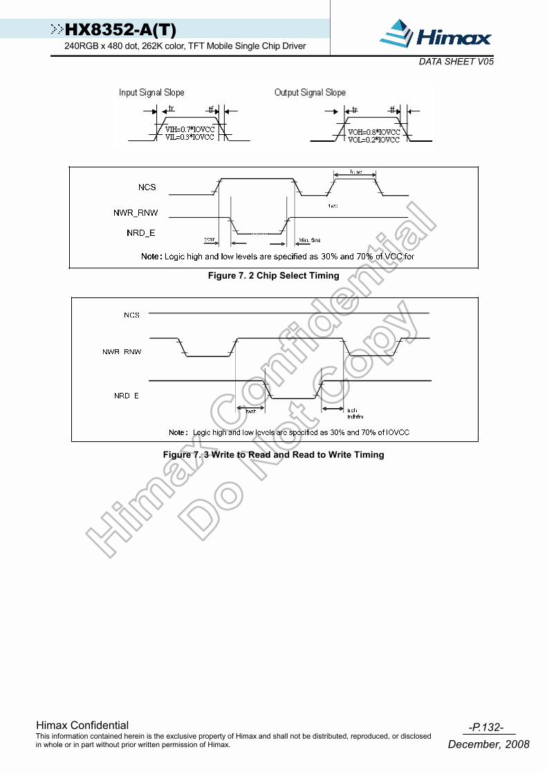
-P.132-Himax Confidential
December, 2008This information contained herein is the exclusive property of Himax and shall not be distributed, reproduced, or disclosed in whole or in part without prior written permission of Himax.
HX8352-A(T) 240RGB x 480 dot, 262K color, TFT Mobile Single Chip Driver
DATA SHEET V05
Figure 7. 2 Chip Select Timing
Figure 7. 3 Write to Read and Read to Write Timing

-P.133-
HX8352-A(T) 240RGB x 480 dot, 262K color, TFT Mobile Single Chip Driver DATA SHEET V04
Himax Confidential This information contained herein is the exclusive property of Himax and shall not be distributed, reproduced, or disclosed in whole or in part without prior written permission of Himax. December, 2008
7.7.2 Parallel interface characteristics (6800-series MPU)
Figure 7. 4 Parallel Interface Characteristics (6800-series MPU)
(VSSA=0V, IOVCC=1.65V to 3.3V, VCC=2.3V TO 3.3V, VCI=2.3V to 3.3V, TA = -30 to 70)
Spec. Signal Symbol Parameter Min. Typ. Max. Unit Description
DNC_SCL tAST
tAHT Address setup time Address hold time (Write/Read)
10 10
- -
- - ns -
NCS
tCHW
tCS
tRCS
tRCSFM
tCSF
tCSH
Chip select “H” pulse width Chip select setup time (Write) Chip select setup time (Read ID)Chip select setup time (Read FM)Chip select wait time(Write/Read)Chip select hold time
0 35
100 100 10 10
- - - - - -
- - - - - -
ns -
NWR_RNW tWC
tWRH
tWRL
Write cycle Control pulse “H” duration Control pulse “L” duration
100 20 20
- - -
- - -
ns -
NRD_E (ID) tRC
tRDH
tRDL
Read cycle (ID) Control pulse “H” duration (ID) Control pulse “L” duration (ID)
150 40 50
- - -
- - -
ns When read ID data
NRD_E (FM)
tRCFM
tRDHFM
tRDLFM
Read cycle (FM) Control pulse “H” duration (FM) Control pulse “L” duration (FM)
250 50
150
- - -
- - -
ns When read from frame memory
DB17~0
Tdst
tDHT
tRAT
tRATFM
tODH
Data setup time Data hold time Read access time (ID) Read access time (FM) Output disable time
20 20 - -
20
- - - - -
- -
70 10080
ns For maximum CL=30pF For minimum CL=8pF
Note: (1) The input signal rise time and fall time (tr, tf) is specified at 15 ns or less. (2) Logic high and low levels are specified as 30% and 70% of IOVCC for Input signals. (3) When normal operation, VDDD=1.65 ~ 2.0V, HX8352-A can meet above timing.

-P.134-Himax Confidential
December, 2008This information contained herein is the exclusive property of Himax and shall not be distributed, reproduced, or disclosed in whole or in part without prior written permission of Himax.
HX8352-A(T) 240RGB x 480 dot, 262K color, TFT Mobile Single Chip Driver
DATA SHEET V05
7.7.3 Serial interface characteristics
Figure 7. 5 Serial Interface Characteristics
Spec. Parameter Symbol Conditions Min. Typ. Max. Unit
Serial clock cycle (Write) DNC_SCL ”H” pulse width (Write) DNC_SCL ”L” pulse width (Write)
tSCYCW
tSHW
tSLW DNC_SCL
100 35 35
- - -
- - -
ns
Data setup time (Write) Data hold time (Write)
tSDS
tSDH SDI 30 30
- -
- - ns
Serial clock cycle (Read) DNC_SCL ”H” pulse width (Read) DNC_SCL ”L” pulse width (Read)
tSCYCR
tSHR
tSLR DNC_SCL
150 60
100
- - -
- - -
ns
Access Time tACC SDO for maximum CL=30pF For minimum CL=8pF
10 - 100 ns
Output disable time tOH SDO For maximum CL=30pF For minimum CL=8pF
15 - 100 ns
DNC_SCL to Chip select tSCC DNC_SCL, NCS 50 - - ns NCS “H” pulse width tCHW NCS 45 - - ns Chip select setup time Chip select hold time
tCSS
tCSH NCS 60 60
- -
- - ns
Note: (1) The input signal rise time and fall time (tr, tf) is specified at 15 ns or less. (2) Logic high and low levels are specified as 30% and 70% of IOVCC for Input signals.
(3) When normal operation, VDDD=1.65 ~ 2.0V, HX8352-A can meet above timing.
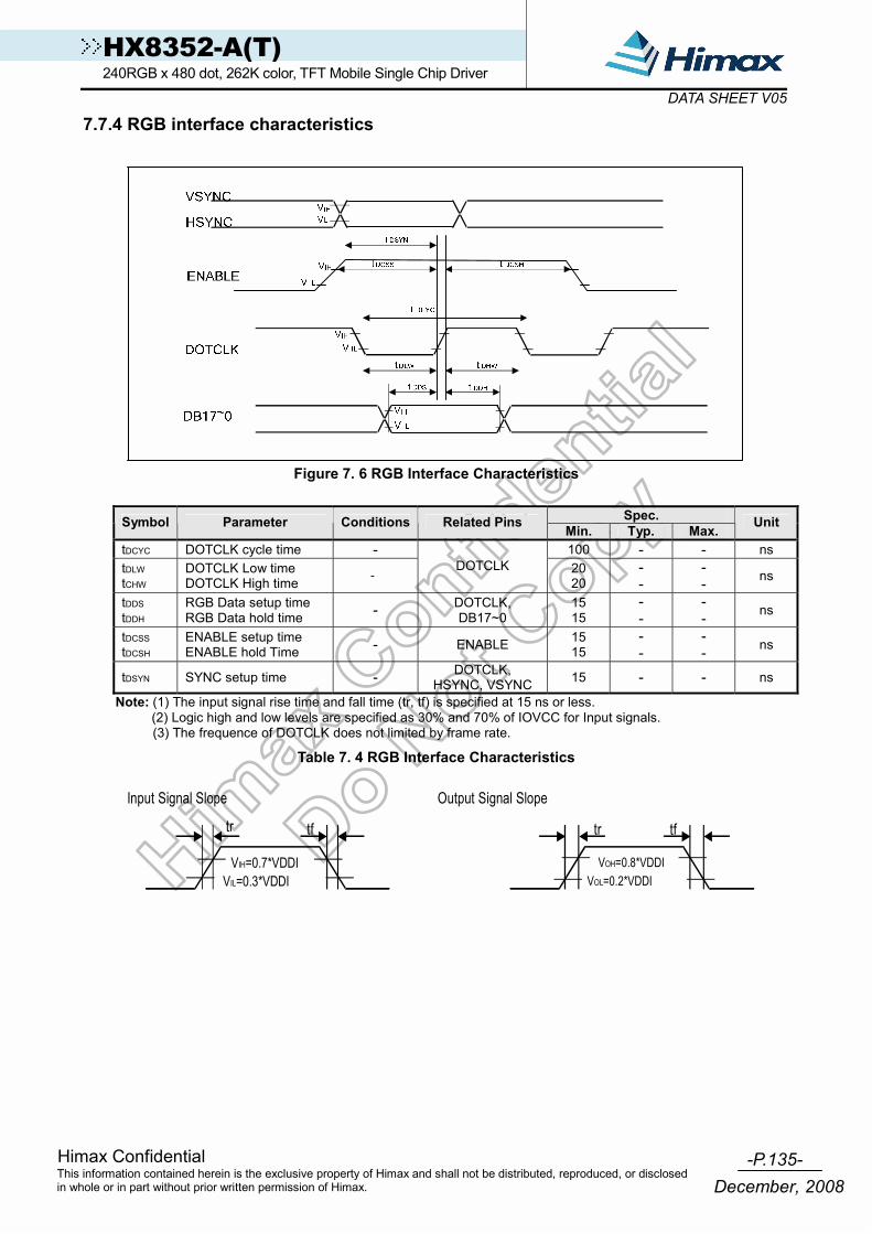
-P.135-Himax Confidential
December, 2008This information contained herein is the exclusive property of Himax and shall not be distributed, reproduced, or disclosed in whole or in part without prior written permission of Himax.
HX8352-A(T) 240RGB x 480 dot, 262K color, TFT Mobile Single Chip Driver
DATA SHEET V05
7.7.4 RGB interface characteristics
Figure 7. 6 RGB Interface Characteristics
Spec. Symbol Parameter Conditions Related Pins Min. Typ. Max. Unit
tDCYC DOTCLK cycle time - 100 - - ns tDLW
tCHW DOTCLK Low time DOTCLK High time -
DOTCLK 20 20
- -
- - ns
tDDS
tDDH RGB Data setup time RGB Data hold time - DOTCLK,
DB17~0 15 15
- -
- - ns
tDCSS
tDCSH ENABLE setup time ENABLE hold Time - ENABLE 15
15 - -
- - ns
tDSYN SYNC setup time - DOTCLK, HSYNC, VSYNC 15 - - ns
Note: (1) The input signal rise time and fall time (tr, tf) is specified at 15 ns or less. (2) Logic high and low levels are specified as 30% and 70% of IOVCC for Input signals. (3) The frequence of DOTCLK does not limited by frame rate.
Table 7. 4 RGB Interface Characteristics
Input Signal Slope
VIH=0.7*VDDIVIL=0.3*VDDI
tr tf
VOH=0.8*VDDIVOL=0.2*VDDI
tr tf
Output Signal Slope

-P.136-Himax Confidential
December, 2008This information contained herein is the exclusive property of Himax and shall not be distributed, reproduced, or disclosed in whole or in part without prior written permission of Himax.
HX8352-A(T) 240RGB x 480 dot, 262K color, TFT Mobile Single Chip Driver
DATA SHEET V05
Note 3 Note 3
TVFPTVFP
TVP
TVDSIPTVBL
VS
DB[17:0]
DE
HS
Vertical Timing for RGB I/F
TCLK
Note 3 Note 3
HS
THFP THFPTHDSIP
THBL
THP
HS
DE
DOTCLK
DB[17:0]
Horizontal Timing for RGB I/F
TVS
TVBP
T
THBP
Specification Item Symbol Condition Min Type. Max Unit
Vertical Timing Vertical cycle period TVP 484 488 496 HS Vertical low pulse width TVS 2 2 HS Vertical front porch TVFP 2 4 HS Vertical back porch TVBP 2 4 HS Vertical blanking period TVBL TVBP + TVFP 4 8 16 HS
HS HS Vertical active area TVDISP
480 HS
Horizontal Timing Horizontal cycle period THP 250 256 290 DOTCLKHorizontal low pulse width THS 2 4 DOTCLKHorizontal front porch THFP 5 8 DOTCLKHorizontal back porch THBP 5 8 DOTCLKHorizontal blanking period THBL THBP + THFP 10 16 50 DOTCLKHorizontal active area THDISP 240 DOTCLK
Pixel clock cycle fCLKCYC 7.5 10.0 MHz
Note 1. IOVCC=1.65 to 3.3V, VCI=2.3 to 3.3V, VSSA=VSSD=0V, Ta=-30 to 70 (to +85 no damage) Note 2. HP is multiples of DOTCLK.
Table 7. 5 Vertical and Horizontal Timing for RGB I/F

-P.137-Himax Confidential
December, 2008This information contained herein is the exclusive property of Himax and shall not be distributed, reproduced, or disclosed in whole or in part without prior written permission of Himax.
HX8352-A(T) 240RGB x 480 dot, 262K color, TFT Mobile Single Chip Driver
DATA SHEET V05
7.7.5 Reset input timing
tRESW
tREST
NRESET
Internal Status
Shorter than 5μs
Normal Operation Resetting Initial Condition(Default for H/W reset)
Figure 7. 7 Reset Input Timing
Spec. Symbol Parameter Related Pins Min. Typ. Max. Note Unit
tRESW Reset low pulse width(1) NRESET 10 - - - µs
- - - 5 When reset applied during “Sleep In mode” ms
tREST Reset complete time(2) - - 120 When reset applied
during “Sleep Out mode” ms
Note: (1)Spike due to an electrostatic discharge on !RES line does not cause irregular system reset according to the following table.
(2)During the resetting period, the display will be blanked (The display is entering blanking sequence,
which maximum time is 120 ms, when Reset Starts in Standby out –mode. The display remains the blank state in Standby In –mode) and then return to Default condition for H/W reset.
(3) During Reset Complete Time, ID2 and VCOMOF value in OTP will be latched to internal register during this period. This loading is done every time when there is H/W reset complete time (tREST) within 5ms after a rising edge of !RES.
(4) Spike Rejection also applies during a valid reset pulse as shown as below:
Symbol Parameter Related Pins Min. Typ. Max. Note UnitT1 Noise of spike NRESET 200(1) - 100(2) - ns Note: (1) Min is mean IOVCC as 1.65V.
(2) Max is mean IOVCC=3.3V. (3) It is necessary to wait 5msec after releasing !RES before sending commands. Also Sleep Out
command cannot be sent for 120msec. Table 7. 6 Reset Input Timing
NRESET Pulse Action Shorter than 5µ Reset Rejected Longer than 10µs Reset Between 5µs and 10µs Reset Start
T1 T1

-P.138-Himax Confidential
December, 2008This information contained herein is the exclusive property of Himax and shall not be distributed, reproduced, or disclosed in whole or in part without prior written permission of Himax.
HX8352-A(T) 240RGB x 480 dot, 262K color, TFT Mobile Single Chip Driver
DATA SHEET V05
8. Reference Applications
8.1 Register- content interface mode
DB1
1 GN
D
DB1
3
NR
ESE
T
EN
ABLE
NR
D_E
DN
C_S
CL
NW
R_R
NW
3. The input pin must be fixed IOVCC or GND when no use. Refer to "Pin Description".
HS
YNC
VSY
NC
2. SDO pin is output pin. SDO pin must be left floating when no use.
SD
O
NC
S
VC
L
VLC
D
DO
TC
LK
VG
L
VG
HVC
I
VR
EG1
IOVC
C
VR
EG3
VC
OM
R
VC
OM
VBG
P
VC
OM
L
VC
OM
H
VD
DD
TE
P68
BS0
BS1
BS2
SD
I
OS
CR
ES
_SEL
0
HSYNCHSYNC
VBGPVBGP
DNC_SCLDNC_SCL
BS2
TEHS
YN
C
ENA
BLE
SDO
SDI
VSYN
C
DO
TC
LK
VCOMVCOM
DN
C_S
CL
NIS
DN
CS
NR
ES
ET
P68
NR
D_E
DB8
NW
R_R
NW
NCSNCS
DB1
4
DB9
DB1
1
P68P68
DB1
5
DB7
DB1
3
R30603/0R
DB1
0
DB1
6
DB3
DB5
DB1
7
VDDDVDDD
DB1
DB6
DB1
2
DB4
BS0
ENABLEENABLE
DB
0
BS1
DB2
NWR_RNWNWR_RNW
Panel resolutionRES_SEL[1:0]
VLCDVLCD
BS1BS1
VCIVCI
BS2BS2
VCOMHVCOMH
BS2P68 BS0BS1
16-bit bus interface, 80-system, 65K-Color
RES_SEL1RES_SEL1
0
0
IOVCCIOVCC
TETE
0
Interface mode
VCOMLVCOML
0
00
SDISDI
10
18-bit bus interface, 80-system, 262K-Color16-bit bus interface, 80-system, 262K-Color
VCOMRVCOMR
VCLVCL
DOTCLKDOTCLK
000
NRESETNRESET
00
1
SDOSDO
11
VSSD
0 8-bit bus interface, 80-system, 65K-Color8-bit bus interface, 80-system, 262K-Color
VC
C
001
VSSA
0
1
1
VGLVGL
00
100
001
VREG3VREG3
1
1
RES_SEL0RES_SEL0
110
011
X
0
ID11
18-bit bus interface, 68-system, 262K-Color16-bit bus interface, 68-system, 262K-Color16-bit bus interface, 68-system, 65K-Color
8-bit bus interface, 68-system, 65K-Color8-bit bus interface, 68-system, 262K-Color
NC
S
IOV
CC
DB1
5
NRD_ENRD_E
NR
ESE
T
VC
I
DB
9D
B8
VREG1VREG1
DB1
2
DB
5D
B4
DB1
0
DB1
4
VGHVGH
DB
6D
B7
NW
R_R
NW
DB
3
R20603/0R
DB
1
NR
D_E
DB
0
DB
2
GN
D
DN
C_S
CL
GN
D
OSCOSC
VSYNCVSYNC
BS0BS0
VC
C
VCCVCC
RE
S_S
EL1
VBG
P
RE
S_S
EL0
EN
ABL
E
DB1
6 VS
YNC
HS
YN
C240RGB x 480 TFT Panel
DO
TC
LK
SD
IS
DO
DB1
7
VDD
D
TE
RE
S_S
EL1
HS
IM_V
CC
VCI
D3RB521S-30
12
VR210K(OPEN)
21
3
C60603/1u/10V
C30603/1u/10V
C11AB0603/2.2u/10V
C70805/1u/25V
D2RB521S-30
1 2
C21AB0603/1u/10V
C140603/1u/10V
TR3
0603
/100
RC5
0805/1u/25V
C100603/1u/10V
IOVCC
TR4
0603
/100
R
OS
C
C20603/1u/10V
C110603/1u/10V
C80603/1u/10V
PW
M_O
UT
C90603/1u/10V
C10603/1u/10V
C22AB0603/1u/10V
C40603/1u/10V
CX11AB0603/2.2u/10V
C120805/1u/25V
NIS
D
NISDNISD
VLC
D
C12AB0603/1u/10V
VCI
D1RB521S-30
12
VRE
G1
VCO
MR
VCL
VCO
M
VCO
MH
VGL
VRE
G3
VCC
VCI
VCO
ML
VGH
R10603/0R
VR1
10K(OPEN)2
1
3
VG
S
HS
IM_V
CC
SPI + RGB interface
PWM
_OU
T
RE
S_S
EL1
RE
S_S
EL0
P68
BS2
BS1
BS0
U1HX8352-AD
UM
MYR
1D
UM
MYR
2V
DD
DV
BG
PV
SSA
VS
SDIO
VC
C
TE
ST1
BS
0
BS
2
TE
ST2
NR
ESE
T
VS
YNC
HS
YN
C
DO
TC
LK
EN
ABL
E
DB
17D
B16
DB
15D
B14
DB
13D
B12
DB
11D
B10
DB
9D
B8
DB
7D
B6
DB
5D
B4
DB
3D
B2
DB
1D
B0
SD
OS
DI
NW
R_R
NW
DN
C_S
CL
TS
3
NR
D_E
TS
2T
S1
TS
0
RE
GVD
D
RE
S_S
EL0
E2
NW
R2
PW
M_O
UT
P68
VG
S
IOG
ND
DU
M1
GP
IO0
GP
IO1
GP
IO2
GP
IO3
GP
IO4
GP
IO5
GP
IO6
GP
IO7
IOG
ND
DU
M2
HS
IM_V
CC
HS
IM_V
SS
IOG
ND
DU
M3
ST
B+IO
GN
DD
UM
4S
TB-
IOG
ND
DU
M5
BS
1
RE
S_S
EL1
RS
2
NC
SN
ISD
BU
RN
TE
TS
8T
S7
TS
6T
S5
TS
4
NC
S2
OS
C
G43
2G
430
G4
G2
G43
1G
429
G3
G1
S1
S2
S3
S72
0S
719
S71
8
DA
TA+
IOG
ND
DU
M6
DA
TA-
IOG
ND
DU
M7
TE
ST_M
OD
ET
EST
_PA
D_D
RV
TE
ST_M
OD
E_C
LK
IOG
ND
DU
M8
VC
OM
VC
OM
HV
CO
ML
VR
EG
1V
CO
MR
VC
LV
GH
VG
LV
RE
G3
VLC
DC
X11
BC
X11
AC
11B
C11
AV
CC
VC
IC
12B
C12
AC
21B
C21
AC
22B
C22
AD
UM
MYR
3D
UM
MYR
4
G42
8
G6
G5
G42
7
VT
EST
G434
G480
G433
G479
EX
TC
TE
ST3
IFSE
L0
IOG
ND
DU
M9
IOG
ND
DU
M10
HS
IM_L
DO
PA
DB0
PA
DB2
PA
DA2
PA
DA0
PA
DB1
PA
DA1
PAD
A4
PAD
A3
PAD
B3
PAD
B4
DM
Y_I
OV
CC
DM
Y_G
ND
DM
Y_I
OV
CC
DM
Y_G
ND
DM
Y_G
ND
DM
Y_I
OV
CC
DM
Y_I
OV
CC
DM
Y_G
ND
DM
Y_I
OV
CC
DM
Y_G
ND
DM
Y_I
OV
CC
DM
Y_I
OV
CC
DM
Y_G
ND
DM
Y_I
OV
CC
DM
Y_G
ND
DM
Y_I
OV
CC
DM
Y_G
ND
DM
Y_I
OV
CC
VSSD
VSSA
GND1GND
GND2GND
J1
FPC56-0.5-4.0L
VCI
1
VCI
2
GN
D3
VCC
4
IOVC
C5
nRES
ET
6
DB1
77
DB1
68
DB1
59
DB1
410
DB1
311
DB1
212
DB1
113
DB1
014
DB
915
DB
816
DB
717
DB
618
DB
519
DB
420
DB
321
DB
222
DB
123
DB
024
nRD
_E25
NW
R_R
NW
26
DN
C_S
CL
27
nCS
28
FLM
29
GN
D30
NC
31
VS
YNC
32
HS
YNC
33
DO
TCLK
34
EN
ABL
E35
SDO
36
SDI
37
NC
38
HSI
M_V
CC
39
HS
IM_V
SS
40
STB
+41
ST
B-42
HS
IM_V
SS
43
DA
TA+
44
DA
TA-
45
HS
IM_V
SS
46
RES
_SEL
147
RES
_SEL
048
EX
TC49
P68
50
BS2
51
BS1
52
BS0
53
GN
D54
BL+
/NC
55
BL_
GN
D/N
C56
1. VCI, IOVCC, VCC are separated from different power source to get better display quality.
00 240RGB x 320 Dot01 240RGB x 400 Dot10 240RGB x 432 Dot11 240RGB x 480 Dot
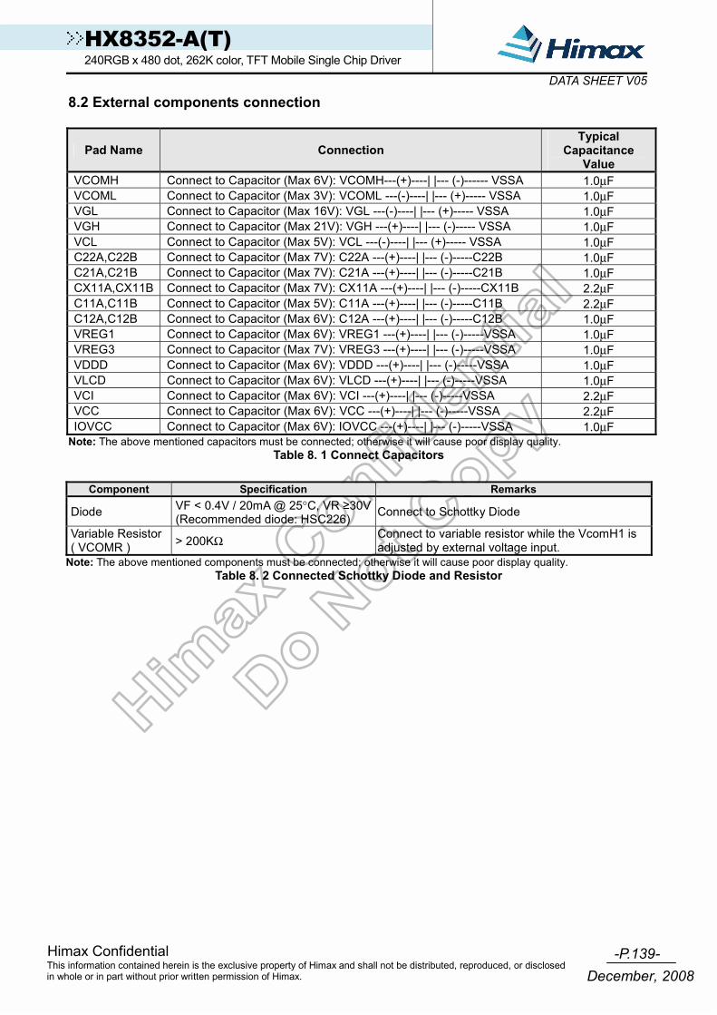
-P.139-Himax Confidential
December, 2008This information contained herein is the exclusive property of Himax and shall not be distributed, reproduced, or disclosed in whole or in part without prior written permission of Himax.
HX8352-A(T) 240RGB x 480 dot, 262K color, TFT Mobile Single Chip Driver
DATA SHEET V05
8.2 External components connection
Pad Name Connection Typical
Capacitance Value
VCOMH Connect to Capacitor (Max 6V): VCOMH---(+)----| |--- (-)------ VSSA 1.0μF VCOML Connect to Capacitor (Max 3V): VCOML ---(-)----| |--- (+)----- VSSA 1.0μF VGL Connect to Capacitor (Max 16V): VGL ---(-)----| |--- (+)----- VSSA 1.0μF VGH Connect to Capacitor (Max 21V): VGH ---(+)----| |--- (-)----- VSSA 1.0μF VCL Connect to Capacitor (Max 5V): VCL ---(-)----| |--- (+)----- VSSA 1.0μF C22A,C22B Connect to Capacitor (Max 7V): C22A ---(+)----| |--- (-)-----C22B 1.0μF C21A,C21B Connect to Capacitor (Max 7V): C21A ---(+)----| |--- (-)-----C21B 1.0μF CX11A,CX11B Connect to Capacitor (Max 7V): CX11A ---(+)----| |--- (-)-----CX11B 2.2μF C11A,C11B Connect to Capacitor (Max 5V): C11A ---(+)----| |--- (-)-----C11B 2.2μF C12A,C12B Connect to Capacitor (Max 6V): C12A ---(+)----| |--- (-)-----C12B 1.0μF VREG1 Connect to Capacitor (Max 6V): VREG1 ---(+)----| |--- (-)-----VSSA 1.0μF VREG3 Connect to Capacitor (Max 7V): VREG3 ---(+)----| |--- (-)-----VSSA 1.0μF VDDD Connect to Capacitor (Max 6V): VDDD ---(+)----| |--- (-)-----VSSA 1.0μF VLCD Connect to Capacitor (Max 6V): VLCD ---(+)----| |--- (-)-----VSSA 1.0μF VCI Connect to Capacitor (Max 6V): VCI ---(+)----| |--- (-)-----VSSA 2.2μF VCC Connect to Capacitor (Max 6V): VCC ---(+)----| |--- (-)-----VSSA 2.2μF IOVCC Connect to Capacitor (Max 6V): IOVCC ---(+)----| |--- (-)-----VSSA 1.0μF
Note: The above mentioned capacitors must be connected; otherwise it will cause poor display quality. Table 8. 1 Connect Capacitors
Component Specification Remarks
Diode VF < 0.4V / 20mA @ 25°C, VR ≥30V(Recommended diode: HSC226) Connect to Schottky Diode
Variable Resistor ( VCOMR ) > 200KΩ Connect to variable resistor while the VcomH1 is
adjusted by external voltage input. Note: The above mentioned components must be connected; otherwise it will cause poor display quality.
Table 8. 2 Connected Schottky Diode and Resistor

-P.140-Himax Confidential
December, 2008This information contained herein is the exclusive property of Himax and shall not be distributed, reproduced, or disclosed in whole or in part without prior written permission of Himax.
HX8352-A(T) 240RGB x 480 dot, 262K color, TFT Mobile Single Chip Driver
DATA SHEET V05
9. Ordering Information
Part No. Package
HX8352-A000 PDxxx PD : mean COG xxx : mean chip thickness (µm), (default: 300 µm)
10. Revision History
Version Date Description of Changes 2007/04/30 New setup 2007/05/08 Update PAD coordinates. 2007/05/10 1. Update 3. Block Diagram.
2. Update DB17~DB0 pin describe in 4.1 Pin Description 3. Modify Figure 6.93 ABC DUTY Control Register. 4. Update Table 7.2.
2007/05/16 1. Change Figure 5.39 Index data from 00202h to 00804h. 2. Change Figure 5.40 Index data from 00202h to 00804h.
2007/05/21 Update OTP Memory table. 2007/05/30 1. Modify Pin number from 435 to 447 in 4.2 Pin
Assignment 2. Modify Pin name in Figure 5.1 ~ 5.6.
2007/06/01 Modify 4.1-Au Bump Size. 2007/07/20 1. Update Gamma formula
2. Modify Figure 5.78 Gamma Resister Stream and Gamma Reference Voltage. 3. Update Table 5.18 Output Voltage of 8 to 1 Selector. 4. Update Command set
2007/08/16 1. Add terminal resistance of 8.2 High speed Interface mode reference applications.
2007/09/06 1. Modify Table 5. 32 EPL Bit Setting and Valid Enable Signal. 2. Modify description of EPL polarity in P150. 3. Modify description of R08h~R09h in P124. 4. Modify description of R22h (Write Data register) in P139.5. Updated Figure 5. 89 Display On/Off Set Sequence. 6. Modify description of R53h in P67. 7. Modify description of R4F in P62. 8. Updated Reference Application circuits in P172~P173. 9. Modify description of Table 5.29 OTP Memory table. 10. Updated Figure 5.86 OTP Progrmming Flow. 11. Updated OTP Programming Sequence in P116. 12. Modify description of R25h ~ R2Ah in P143.
2007/09/19 1. Modify description of Register Access Packet in P53. 2007/10/29 1. Modify Pin Description of High speed part in P14~P15. 2007/11/01 1. Modify OTP table in P114.
2. Modify register table in P120. 3. Add new register (R00h) in P122. 4. Modify RTN table in P146. 5. Add Value of AC Characteristics in P166 ~ P170.
01
2007/11/21 1. Modify R56h ~ R59h index value in P158~P159. 2. Modify step 14 of PROGRAM SEQUENCE in P116. 3. Modify description of IDMON in P122.

-P.141-Himax Confidential
December, 2008This information contained herein is the exclusive property of Himax and shall not be distributed, reproduced, or disclosed in whole or in part without prior written permission of Himax.
HX8352-A(T) 240RGB x 480 dot, 262K color, TFT Mobile Single Chip Driver
DATA SHEET V05
200712/24 1. Modify pin description in P15.
2. Add new register R95h, R96h andR97h in Register table in p121.
3. Modify N_SAP table in P151. 4. Modify description of R5Ch in P160. 5. Add new register R95h, R96h andR97h in P161-P162. 6. Modify Splike rejection of Reset input timing in P173.
2008/01/09 1. Remove SPI Write GRMA timing In P44. 2. Modify OTP table in P112. 3. Modify AC Characteristics in P164 ~ P168.
02
2008/03/11 1. Add new register R83h in P159. 2. Add new register R85h in P159. 3. Add new register R8Bh and R8Ch in P160. 4. Modify description of R95h in P161. 5. Modify description of R97h in P162.
2008/03/21 1. Modify OTP table in P112. 03 2008/05/09 1. Remove High speed Interface.
2. Add new register (R6Fh ~ R77h). 04 2008/08/12 1. Remove preliminary in the datasheet. 05 2008/12/24 1. Modify description of RES(1-0) setting in P12.
2. Modify R1Bh (AP table) in P98. 3. Add new register R8Ah in P123. 4. Add R6Bh and R6Ch (PWM period control setting
register) in P125. 5. Add table 7.5 porch setting of RGB IF in P136.
With collaboration of https://www.displayfuture.com