scanning probe microscopy conductivity measurements of …...solar cells belong to 2nd generation,...
TRANSCRIPT
MASTER THESIS
Scanning Probe Microscopy Conductivity Measurements of InP Nanowires for Solar
cells Division of Synchrotron Radiation Research
Department Of Physics
Mubashar Irfan
28 Feburary 2013
Supervisor & Co-supervisor.
Rainer Timm
Anders Mikkelsen

1
Abstract
This thesis is devoted to the analysis of the I-V properties of axial InP pn-junction
nanowires made for solar cell application. A novel method has been used to measure the I-V
characteristics very accurately and reproducibly, using scanning tunneling microscopy (STM).
The STM is used to first image the nanowires from top and then form a low resistive point
contact between the STM tip and an individual nanowire, which is still on its growth substrate, in
ultrahigh vacuum conditions. This setup is well suited to investigate the I-V characteristics of
individual nanowires with high accuracy and statistical relevance.
In particular, the I-V curves are first analyzed to evaluate when a low resistive point
contact has been established. Then, I-V characteristics of nanowires before and after sample
cleaning are obtained in order to compare the effect of the surface oxide layer on the nanowire
electric properties. The InP pn-junction nanowires show rectifying behavior with typical ideality
factors between 2.5 and 2.6. When the surface oxide is removed from the nanowires by
annealing under atomic hydrogen background, the ideality factor slightly improves and the
conductivity of the individual nanowires increases dramatically for both reverse and forward
bias.

2
Acknowledgements
I would especially like to thank my supervisor Rainer Timm and co-supervisor Anders
Mikkelson for their guidance, their kind manner and solving all my questions, and also their
willingness to invest time in educating me on this work. I also very thankful to them for putting
in hours of their own time to guide me through all my experimental work and providing me the
knowledge of my work.
Further I would like to give special thanks to all my friends and colleagues, who
supported me through the tough times. Also Cheers to Tomas Brage, Carl-Erik Magnusson, the
Department of physics, the Department of Synchrotron radiation research and to the Government
of Sweden to give me the opportunity to complete my study at Lund university.
Last but not least, I would like to especially thank my parents and family who have
supported me throughout my whole study. Without the support of my father and prayers of my
mother I could not complete my study.
3
Table of Contents
Abstract ..................................................................................................................................................... 1
Acknowledgements ................................................................................................................................... 2
Table of Contents .......................................................................................................................................... 3
1. Introduction .......................................................................................................................................... 5
1.1 Motivation. .................................................................................................................................... 5
1.2 Thesis Outline ............................................................................................................................... 7
2. Scientific and Technological Background .............................................................................................. 8
2.1. Fundamental of photovoltaic operation ........................................................................................ 8
2.1.1 Doping ................................................................................................................................... 8
2.1.2. PN-junction ......................................................................................................................... 10
2.1.3 Solar cell ............................................................................................................................. 11
2.2 Nanowires ................................................................................................................................... 13
2.2.1 Nanowire growth................................................................................................................. 13
2.2.2 Nanowire Doping ................................................................................................................ 16
2.2.3 Nanowire Solar cell. ............................................................................................................ 17
2.3. IV characteristics of ideal diode .................................................................................................. 18
2.4. IV characteristics of the solar cell ............................................................................................... 20
3. Experimental Technique ..................................................................................................................... 21
3.1 Scanning tunneling Microscopy .................................................................................................. 21
3.2 Experimental Setup ..................................................................................................................... 23
3.2.1 Equipment ........................................................................................................................... 23
3.3. Experimental procedure .............................................................................................................. 23
3.3.1 Scanning Electron microscopy ............................................................................................ 24
3.3.2 Tip etching and preparation ................................................................................................ 25
3.3.3 Sample fabrication and preparation .................................................................................... 25
3.3.4 STM Tip –Sample approach for nanowire sample.............................................................. 26
3.3.5 STM imaging and formation of point contact ..................................................................... 26
3.3.6 Electrical measurements ..................................................................................................... 27
4. Result and Discussion .......................................................................................................................... 28

4
4.1 Establishing a low resistive point contact ................................................................................... 28
4.2 I-V characteristic of the InP pn-junction nanowires ................................................................... 30
4.2.1 Nanowires with native oxide ............................................................................................... 31
4.2.2 Cleaned nanowire ................................................................................................................ 33
4.2.3 Discussion ........................................................................................................................... 34
5. Conclusion and outlook ...................................................................................................................... 37
5.1 Conclusion .................................................................................................................................. 37
5.2 Outlook ....................................................................................................................................... 37
Bibliography ................................................................................................................................................ 39
5
1. Introduction
1.1 Motivation.
Solar energy is the most plentiful renewable energy source, which also is available
everywhere on the earth. The solar energy that reaches the earth is about 5000 times the current
energy demand [1]. Considering the increasing oil prices and the effects of carbon dioxide on
climate, solar energy is the most important energy source, which is clean and renewable.
Consequently, many efforts have been devoted to the development of new material and devices
that can convert solar energy into any other form of energy. One of the most popular approaches
is to use photovoltaic cells, which have the potential to harvest the solar energy and convert into
electricity [2].
Semiconductor materials have been under investigation for photovolotaic devices since
1950 [2]. In the evaluation of efficiency, the development in PV technology is divided into three
generations [3]. For over two decades 1st generation crystalline silicon solar cells have been used
for photovoltaic and maximum efficiency recorded is 24% [4]. Later on, the developments in PV
solar cells belong to 2nd
generation, which consists of thin-film based technology. The
production cost of thin-film technology is much less than crystalline silicon technology, but the
efficiency of crystalline PV is not yet reached. Typical thin-film based solar cells have only an
efficiency of 10 to 16% [5]. Third generation solar cells, including tandem cells and multi-
junction semiconductor solar cells have obtained highest efficiency, but at much higher cost. III-
V compound semiconductor materials are normally used due to their high material quality and
optimized band gaps. A 40% efficiency has been recorded for GaInP/GaInAs/Ge three junction
solar cells [6].
Moreover, to increase the efficiency and reduce the cost and size the nanowires play an
important role in solar cell research. The controled synthesis approaches used to fabricate
nanowires have also improved the efficiency of the PV solar cell. The use of semiconductor
6
nanowires for PV applications has many advantages over thin film solar cell and conventional
crystalline solar cell technologies for several reasons. In particular, it allows a long absorption
path along the length of the wire, efficient carrier extraction, strong light trapping, and
modification of material properties [7]. III-V semiconductor NWs are currently being explored
as key building block for optical and electronic devices. The solar cell based on these NWs has
shown great potential superior to the bulk structure, because they are flexible in combination of
material, and they can be integrated on a silicon platform to reduce the cost and material
consumption. Many different semiconductor materials have been synthesized to fabricate
nanowire photovoltaics, such as silicon, germanium, zinc oxide, zinc sulfide, cadmium telluride,
cadmium selenide, copper oxide, titanium oxide, gallium nitride, indium gallium nitride, gallium
arsenide and indium phosphide [8].
Despite the advantages of the nanowire solar cell, there are still several fundamental
challenges for future research activities. The most important are surface and interface
recombination, stability and choice of semiconductor materials, control of growth and doping,
and nanowire array uniformity. Much development has been done in these areas, but more work
is needed to understand the surface and interface of semiconductor materials [8, 9]. Very
recently, researchers at Lund university have significantly improved the efficiency of single-
junction NW solar devices to 13.8% by increasing the NW volume fraction, developing surface
passivation, evaluating doping levels and optimizing processes [10].
The small lateral dimension of the nanowires enables high performance material.
However, it is still a major challenge to measure the electrical properties of the individual NWs.
The conventional field-effect transistor setup has been widely used to investigate the electrical
properties of nanowires, where the nanowires are deposited on an insulated substrate. The
nanowires are identified by optical microscopy or scanning electron microscopy (SEM), and then
contacted with metallic electrodes using electron beam lithography. But in this method the
measured I-V characteristics of nanowires are significantly affected by the contacts between
semiconductor nanowires and the metal electrodes [11]. Therefore we have used a noval method
to measure the I-V characteristics of individual nanowires still standing upright on their growth
substrate, using STM without any additional microscopy tool or sample processing. The STM is
first used for finding the nanowires and forming of point contact directly between the probe tip

7
and the nanowire grown on the substrate in ultrahigh vacuum condition. The ultrahigh vacuum
condition provides a clean and well controlled enviorment which results in a low resistive point
contact. Also a speciality of the STM setup is the possibility to interrupt the feedback loop
between the STM and its control unit and allow it to contact with the external circuit.
1.2 Thesis Outline
The main section of this thesis is devided into five chapters including the introduction,
technique, results and discussion part. The motivation of this thesis is discussed in the first
chapter named introduction.
The second chapter “Scientific and Technological Background” deals with the
Fundamentals of photovoltaics, nanowires and electrical characterization of solar cells.
The third chapter contains the theory about the experimental technique used in this
thesis. The experimental setup and procedure is also part of this chapter.
In the fourth chapter the main results of the experiment are described and discussed.
The conclusion of this work is discussed in chapter five.

8
2. Scientific and Technological Background
2.1. Fundamentals of photovoltaic operation
Photovoltaic (PV) technology enables us to convert sunlight directly into electricity. The
term “photo” means light and “voltaic” relates to the production of electricity [12]. A
photovoltaic cell, also called “Solar cell” is a pn-junction made of semiconductor material with
large surface area, producing electricity when sunlight falls on it [13]
In order to understand the operation of the PV cell, one has to firstly understand the basic
principle of the pn-junction.
2.1.1 Doping
The phenomenon in which impurity atoms are introduced into semiconductor material is
called doping. The electrical conductive properties of the material can be controlled by these
impurity atoms. Traditionally, group IV elements have been used as a semiconductor material for
a long time, but within the last decade compound materials, usually from groups III and V have
been introduced as semiconductor material. Such materials have the advantage of a direct band
gap and higher charge mobility. The doping of these compound semiconductors is discussed
later. Let us first consider a typical group IV semiconductor material like Silicon or Germanium.
These elements have four electrons in the valence shell. There are two types of doping, n-type
doping and p-type doping. N-type doping involves substituting a silicon or germanium atom by
group V element impurity such as phosphorus, arsenic or antimony. If one impurity atom is
added in silicon, the four valence electrons of silicon make covalent bonds with the nearest
neighbor electrons of the impurity atom, leaving one extra electron. This extra electron
contributes to increase the conductivity of the semiconductor material.
If the substituting impurity atom is a group III element, three of the silicon electrons
make a covalent bond with the nearest neighbor, leaving one hole behind. The movement of a
hole in one direction corresponds to the movement of an electron in the other direction and also

9
affects the conductivity of the material. These types of materials are called p-type
semiconductors [14].
The group V impurity atom is also called donor, because it can donate one electron to the
conduction band of the semiconductor, when a small amount of energy is given to it. The
electron in the conduction band can move through the whole material, leaving behind a fixed
positively charged ion and generate a current. Similarly, the impurity of group III element
accepts an electron from the valence band, leaving behind a hole in the valence band and so is
called an acceptor atom. In this case the hole can move through the material without generating
an electron in the conduction band. In the presence of an applied electric field these free charge
carriers will move and generate electric current. The energy band diagrams of donor and
acceptor are shown in Fig 1(a,b) [15].
Figure 1 : The Fermi energy level, conduction band edge, and valence band edge are represented by
EF , Ec and EV. (a) the donor energy state and (b) the acceptor energy state [15].
10
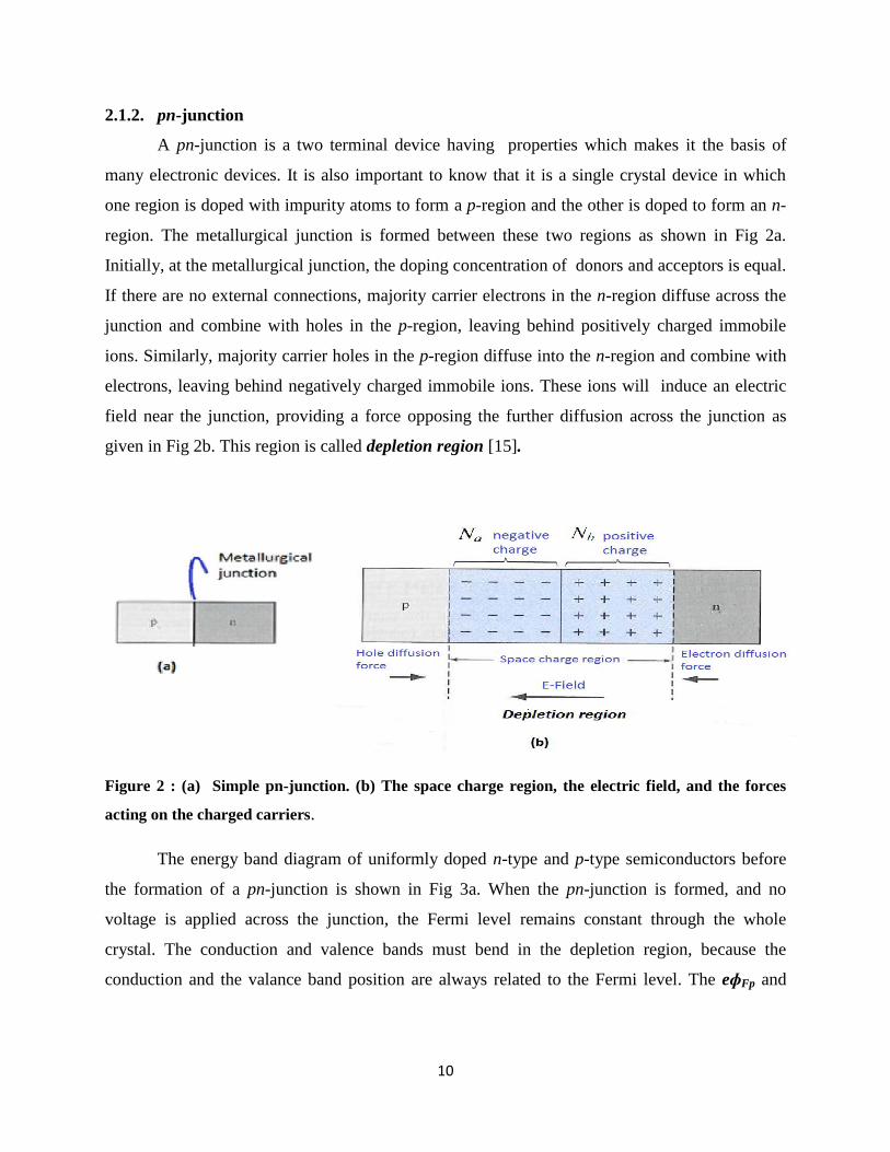
2.1.2. pn-junction
A pn-junction is a two terminal device having properties which makes it the basis of
many electronic devices. It is also important to know that it is a single crystal device in which
one region is doped with impurity atoms to form a p-region and the other is doped to form an n-
region. The metallurgical junction is formed between these two regions as shown in Fig 2a.
Initially, at the metallurgical junction, the doping concentration of donors and acceptors is equal.
If there are no external connections, majority carrier electrons in the n-region diffuse across the
junction and combine with holes in the p-region, leaving behind positively charged immobile
ions. Similarly, majority carrier holes in the p-region diffuse into the n-region and combine with
electrons, leaving behind negatively charged immobile ions. These ions will induce an electric
field near the junction, providing a force opposing the further diffusion across the junction as
given in Fig 2b. This region is called depletion region [15].
Figure 2 : (a) Simple pn-junction. (b) The space charge region, the electric field, and the forces
acting on the charged carriers.
The energy band diagram of uniformly doped n-type and p-type semiconductors before
the formation of a pn-junction is shown in Fig 3a. When the pn-junction is formed, and no
voltage is applied across the junction, the Fermi level remains constant through the whole
crystal. The conduction and valence bands must bend in the depletion region, because the
conduction and the valance band position are always related to the Fermi level. The eɸFp and

11
eɸFn are the difference in energy between the Fermi-level and the intrinsic Fermi-level at the p-
and n-side of the junction. Fig 3b shows the energy level diagram of the pn-junction.
Figure 3 : (a) Position of Fermi-level for n-type and p-type semiconductors (b) Energy-band
diagram of a pn junction in thermal equilibrium [15].
The difference in work function of the n-type and p-type semiconductor causes the
internal potential near the junction, which is called built-in potential. It is represented by Vbi and
is equal to the sum of eɸFp and eɸFn . The built-in potential maintains the equilibrium between
majority and minority carriers in n-type and p-type region. This potential only maintains the
equilibrium, so no current will be produced by this voltage. The potential energy corresponding
to this potential is eVbi.
2.1.3 Solar cell
A solar cell is an electrical device that converts the solar light energy into electricity by
the photovolatic effect and delivers this energy to a load. The first solar cell was developed at
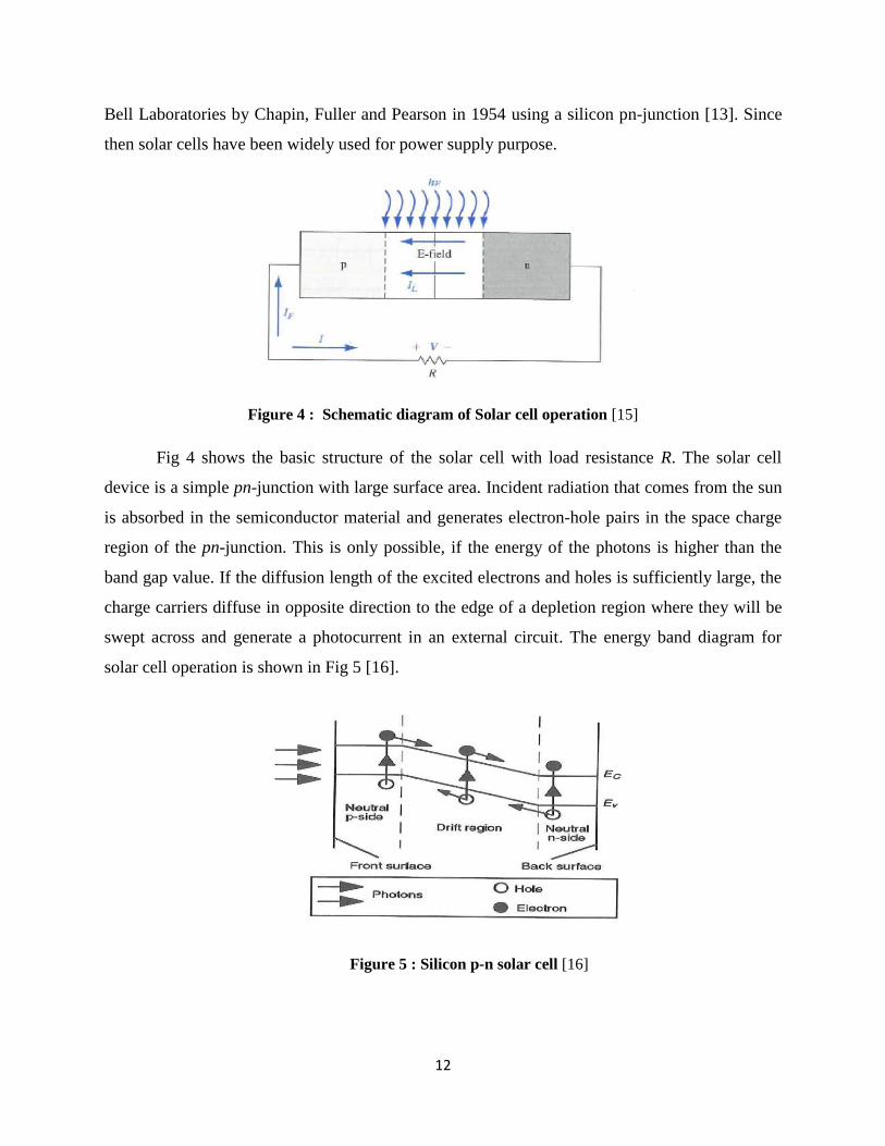
12
Bell Laboratories by Chapin, Fuller and Pearson in 1954 using a silicon pn-junction [13]. Since
then solar cells have been widely used for power supply purpose.
Figure 4 : Schematic diagram of Solar cell operation [15]
Fig 4 shows the basic structure of the solar cell with load resistance R. The solar cell
device is a simple pn-junction with large surface area. Incident radiation that comes from the sun
is absorbed in the semiconductor material and generates electron-hole pairs in the space charge
region of the pn-junction. This is only possible, if the energy of the photons is higher than the
band gap value. If the diffusion length of the excited electrons and holes is sufficiently large, the
charge carriers diffuse in opposite direction to the edge of a depletion region where they will be
swept across and generate a photocurrent in an external circuit. The energy band diagram for
solar cell operation is shown in Fig 5 [16].
Figure 5 : Silicon p-n solar cell [16]
13
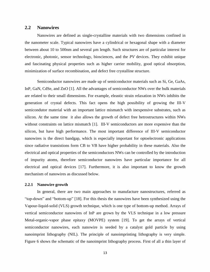
2.2 Nanowires
Nanowires are defined as single-crystalline materials with two dimensions confined in
the nanometer scale. Typical nanowires have a cylindrical or hexagonal shape with a diameter
between about 10 to 500nm and several µm length. Such structures are of particular interest for
electronic, photonic, sensor technology, biosciences, and the PV devices. They exhibit unique
and fascinating physical properties such as higher carrier mobility, good optical obsorption,
minimization of surface recombination, and defect free crystalline structure.
Semiconductor nanowires are made up of semiconductor materials such as Si, Ge, GaAs,
InP, GaN, CdSe, and ZnO [1]. All the advantages of semiconductor NWs over the bulk materials
are related to their small dimensions. For example, eleastic strain relaxation in NWs inhibits the
generation of crystal defects. This fact opens the high possibility of growing the III-V
semicondutor material with an important lattice mismatch with inexpensive substrates, such as
silicon. At the same time it also allows the growth of defect free hetrostructures within NWs
without constraints on lattice mismatch [1]. III-V semiconductors are more expensive than the
silicon, but have high performance. The most important difference of III-V semiconductor
nanowires is the direct bandgap, which is especially important for optoelectronic applications
since radiative transistions form CB to VB have higher probability in these materials. Also the
electrical and optical properties of the semiconductors NWs can be controlled by the introduction
of impurity atoms, therefore semiconductor nanowires have particular importance for all
electrical and optical devices [17]. Furthermore, it is also important to know the growth
mechanism of nanowires as discussed below.
2.2.1 Nanowire growth
In general, there are two main approaches to manufacture nanostructures, referred as
“top-down” and “bottom-up” [18]. For this thesis the nanowires have been synthesized using the
Vapour-liquid-solid (VLS) growth technique, which is one type of bottom-up method. Arrays of
vertical semiconductor nanowires of InP are grown by the VLS technique in a low pressure
Metal-organic-vapor phase epitaxy (MOVPE) system [19]. To get the arrays of vertical
semiconductor nanowires, each nanowire is seeded by a catalyst gold particle by using
nanoimprint lithography (NIL). The principle of nanoimprinting lithography is very simple.
Figure 6 shows the schematic of the nanoimprint lithography process. First of all a thin layer of

14
the imprint resist material is coated onto the sample substrate. A stamp or mold with predefined
monolithic silicon structure is pressed into the resist material at controlled temperature and
pressure for imprinting process. The sample is then cleaned to remove surface oxide. Afterwards
a thin gold film is deposited via thermal evaporation in the vaccum chamber. At the end the rest
of resist material is removed with part of gold layer covering it [20].
Figure 6: Schematic of the nanoimprint lithography. (a,b) imprint process using stamp. (c,d)
deposition of gold particle and pattern transfer.
After the nanoimprint lithography, the substrate with gold particles is introduced into the
low-pressure MOVPE system and placed on an RF-heated graphite susceptor. In order to anneal
the sample, the temperature is increased to 5800C, which is above the desired growth temperature
in the presence of the group V precursor . This step aids in the desorption of surface oxide, and
alloys the Au-particle with the InP substrate. A group V precursor background is used to reduce
the decomposition of the InP substrate at elevated temperature. After annealing, the temperature
is ramped down to 4000C. Nanowire growth is started under the Au-particle, when the constant
flow of group III and group V precursors are introduced into the reactor. Finally, the sample is
cooled down to room temperature. The different steps involved in MOVPE system are shown in
Fig 7.

15
Figure 7 : Schematic view of nanowire growth mechanism in MOVPE. (a) Au particles are
deposited on a substrate. (b) Desorption of oxide surface using high temperature under group V
pressure. (c) III-V precursors are supplied for growth process. (d) The nanowires after growth.
Uniform arrays of vertical InP nanowires are obtained where the diameter of the
nanowire is directly controlled by the catalyzed Au-particle, and the length is determined by
growth time. The location of the nanowire is defined by nanoimprint lithography [20].
The nanowires are typically grown in the direction perpendicular to the closed-packed
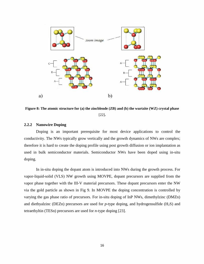
planes in the crystal structure. In contrast to the bulk crystal phase, nanowires exhibit the zinc
blende (ZB), wurtzite (WZ), or a combination of both structures depending on the growth
parameters (temperature, doping, gas flux) and diameter [1]. The crystal structure of the
nanowires is important since it affects the electronic and optical properties of the materials. The
atomic arrangements of the ZB structure and WZ structure are illustrated in Figure 8. The
Bravais lattice of the ZB and WZ crystal structure are cubic and hexagonal, respectively. They
can be distinguished by the stacking sequence of each bilayer. The ZB stacking sequence is
described as ABCABC……, and for WZ it is described as ABAB……… [21].
16
Figure 8: The atomic structure for (a) the zincblende (ZB) and (b) the wurtzite (WZ) crystal phase
[22].
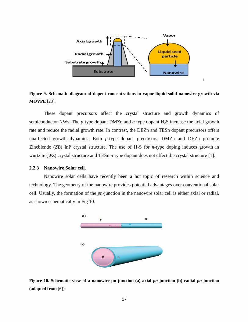
2.2.2 Nanowire Doping
Doping is an important prerequisite for most device applications to control the
conductivity. The NWs typically grow vertically and the growth dynamics of NWs are complex;
therefore it is hard to create the doping profile using post growth diffusion or ion implantation as
used in bulk semiconductor materials. Semiconductor NWs have been doped using in-situ
doping.
In in-situ doping the dopant atom is introduced into NWs during the growth process. For
vapor-liquid-solid (VLS) NW growth using MOVPE, dopant precursors are supplied from the
vapor phase together with the III-V material precursors. These dopant precursors enter the NW
via the gold particle as shown in Fig 9. In MOVPE the doping concentration is controlled by
varying the gas phase ratio of precursors. For in-situ doping of InP NWs, dimethylzinc (DMZn)
and diethyalzinc (DEZn) precursors are used for p-type doping, and hydrogensulfide (H2S) and
tetraethyltin (TESn) precursors are used for n-type doping [23].
17
i
Figure 9. Schematic diagram of dopent concentrations in vapor-liquid-solid nanowire growth via
MOVPE [23].
These dopant precursors affect the crystal structure and growth dynamics of
semiconductor NWs. The p-type dopant DMZn and n-type dopant H2S increase the axial growth
rate and reduce the radial growth rate. In contrast, the DEZn and TESn dopant precursors offers
unaffected growth dynamics. Both p-type dopant precursors, DMZn and DEZn promote
Zincblende (ZB) InP crystal structure. The use of H2S for n-type doping induces growth in
wurtzite (WZ) crystal structure and TESn n-type dopant does not effect the crystal structure [1].
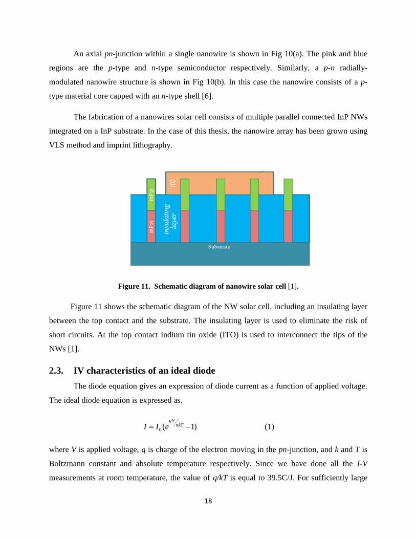
2.2.3 Nanowire Solar cell.
Nanowire solar cells have recently been a hot topic of research within science and
technology. The geometry of the nanowire provides potential advantages over conventional solar
cell. Usually, the formation of the pn-junction in the nanowire solar cell is either axial or radial,
as shown schematically in Fig 10.
Figure 10. Schematic view of a nanowire pn-junction (a) axial pn-junction (b) radial pn-junction
(adapted from [6]).
18
An axial pn-junction within a single nanowire is shown in Fig 10(a). The pink and blue
regions are the p-type and n-type semiconductor respectively. Similarly, a p-n radially-
modulated nanowire structure is shown in Fig 10(b). In this case the nanowire consists of a p-
type material core capped with an n-type shell [6].
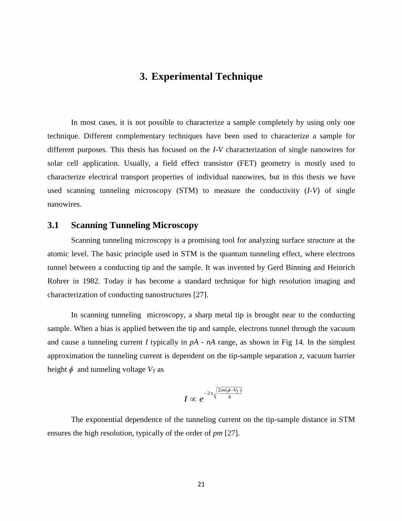
The fabrication of a nanowires solar cell consists of multiple parallel connected InP NWs
integrated on a InP substrate. In the case of this thesis, the nanowire array has been grown using
VLS method and imprint lithography.
Figure 11. Schematic diagram of nanowire solar cell [1].
Figure 11 shows the schematic diagram of the NW solar cell, including an insulating layer
between the top contact and the substrate. The insulating layer is used to eliminate the risk of
short circuits. At the top contact indium tin oxide (ITO) is used to interconnect the tips of the
NWs [1].
2.3. IV characteristics of an ideal diode
The diode equation gives an expression of diode current as a function of applied voltage.
The ideal diode equation is expressed as.
)1(0 nkTqV
eII (1)
where V is applied voltage, q is charge of the electron moving in the pn-junction, and k and T is
Boltzmann constant and absolute temperature respectively. Since we have done all the I-V
measurements at room temperature, the value of q/kT is equal to 39.5C/J. For sufficiently large

19
forward bias (V >> 1/40V) the exponential term is very large, so we can neglect the term ‘1’ in
the diode equation. However, for non-ideal diodes, different mechanisms (generation-
recombination, series resistance effect) decrease the slope of the I-V curve, resulting in
nkTqV
eII 0 (2)
nkT
qVI )ln( (3)
where n is called ideality factor. It is a measure of how closely the diode follows the ideal diode
equation meaning that for an ideal diode the ideality factor is n = 1 [24]. According to eq. (3), by
plotting ln(I) against V we should obtain a straight line if the diode was ideal, as shown in Fig
13. When a real diode is considered, different effects change the slope in different voltage
regions, as shown in Fig 12(b). In general the intermediate voltage region is best for linear
fitting, because the slope is steepest and most linear here, coming closest to the ideal diode case
with n = 1. The voltage where the slope starts to be steep and linear is called on-set voltage. By
determining the slope (m) of the linear fit in this region of the real diode, we can obtain the
ideality factor using the equation:
mn 5.39 , (4)
Figure 12. (a) I-V characteristics of a pn-juntion in logarithmic plot to measure the slope for
forward bias and in inset linear curve for the same nanowire and I-V measurement (b) Logarithmic
plot with all effects in different voltage regions [25].

20
2.4. IV characteristics of the solar cell
The electrical transport properties of the solar cell are characterized by the current-
voltage (I-V) measurement, under the dark and the illuminated condition at room temperature. In
the dark condition the solar cell behaves like an ideal diode.
The two basic parameters that characterize the solar cell are the open-circuit voltage and
short-circuit current denoted by Voc and Isc respectively. The voltage of the solar cell in the case
of zero current flow is called open-circuit voltage. Similarly, the current through the circuit when
no voltage is applied across the device is called short-circuit current as sketched in Fig 13 [26].
Figure 13: I-V characteristic curves of a solar cell with and without illumination [26].
21
3. Experimental Technique
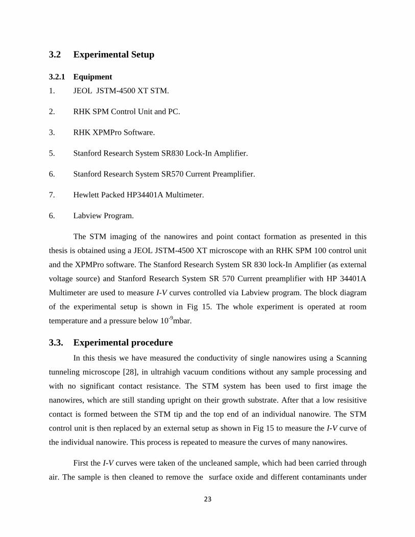
In most cases, it is not possible to characterize a sample completely by using only one
technique. Different complementary techniques have been used to characterize a sample for
different purposes. This thesis has focused on the I-V characterization of single nanowires for
solar cell application. Usually, a field effect transistor (FET) geometry is mostly used to
characterize electrical transport properties of individual nanowires, but in this thesis we have
used scanning tunneling microscopy (STM) to measure the conductivity (I-V) of single
nanowires.
3.1 Scanning Tunneling Microscopy
Scanning tunneling microscopy is a promising tool for analyzing surface structure at the
atomic level. The basic principle used in STM is the quantum tunneling effect, where electrons
tunnel between a conducting tip and the sample. It was invented by Gerd Binning and Heinrich
Rohrer in 1982. Today it has become a standard technique for high resolution imaging and
characterization of conducting nanostructures [27].
In scanning tunneling microscopy, a sharp metal tip is brought near to the conducting
sample. When a bias is applied between the tip and sample, electrons tunnel through the vacuum
and cause a tunneling current I typically in pA - nA range, as shown in Fig 14. In the simplest
approximation the tunneling current is dependent on the tip-sample separation z, vacuum barrier
height ɸ and tunneling voltage VT as
)(22 TVm
z
eI
The exponential dependence of the tunneling current on the tip-sample distance in STM
ensures the high resolution, typically of the order of pm [27].

22
Figure 14. Schematic drawing of a STM setup [21].
Basically, the STM can be operated in two modes to take images. For this thesis the STM
was operated in constant current mode, in which the tip is scanned over the surface in x-y-plane
while the tunneling current remains constant using a feedback loop. To maintain the constant
current the tip and height is adjusted to the sample morphology along the z-axis using a
piezoelectric tube, which can expand or contract if the bias voltage is applied. The z-
displacement of the tip is recorded and converted into a color scale STM image, representing the
sample topography. The other STM operation mode is a constant height mode, in which the
height of tip remains constant, while the change in tunneling current is recorded and translated
into images. The benefit of this mode is that it is faster than the constant current mode. But it can
only be applied for flat sample surface, because otherwise the surface corrugation causes the tip
to crash [21].
In order to get high resolution images at the atomic level, the tip and sample should be
clean during the scanning process. This is only possible when the STM works under ultra high
vacuum (UHV) conditions. The STM can also be used in air, water, and other liquids for many
other applications [5]. The other prerequisite for high resolution images is excellent vibration
isolation, and mechanical springs or gas damping are often used to reduce external vibrations.
23
3.2 Experimental Setup
3.2.1 Equipment
1. JEOL JSTM-4500 XT STM.
2. RHK SPM Control Unit and PC.
3. RHK XPMPro Software.
5. Stanford Research System SR830 Lock-In Amplifier.
6. Stanford Research System SR570 Current Preamplifier.
7. Hewlett Packed HP34401A Multimeter.
6. Labview Program.
The STM imaging of the nanowires and point contact formation as presented in this
thesis is obtained using a JEOL JSTM-4500 XT microscope with an RHK SPM 100 control unit
and the XPMPro software. The Stanford Research System SR 830 lock-In Amplifier (as external
voltage source) and Stanford Research System SR 570 Current preamplifier with HP 34401A
Multimeter are used to measure I-V curves controlled via Labview program. The block diagram
of the experimental setup is shown in Fig 15. The whole experiment is operated at room
temperature and a pressure below 10-9
mbar.
3.3. Experimental procedure
In this thesis we have measured the conductivity of single nanowires using a Scanning
tunneling microscope [28], in ultrahigh vacuum conditions without any sample processing and
with no significant contact resistance. The STM system has been used to first image the
nanowires, which are still standing upright on their growth substrate. After that a low resisitive
contact is formed between the STM tip and the top end of an individual nanowire. The STM
control unit is then replaced by an external setup as shown in Fig 15 to measure the I-V curve of
the individual nanowire. This process is repeated to measure the curves of many nanowires.
First the I-V curves were taken of the uncleaned sample, which had been carried through
air. The sample is then cleaned to remove the surface oxide and different contaminants under
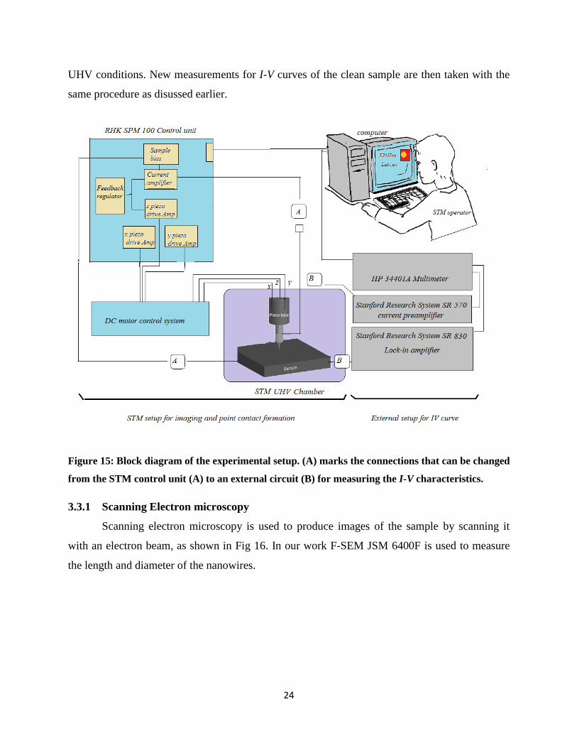
24
UHV conditions. New measurements for I-V curves of the clean sample are then taken with the
same procedure as disussed earlier.
Figure 15: Block diagram of the experimental setup. (A) marks the connections that can be changed
from the STM control unit (A) to an external circuit (B) for measuring the I-V characteristics.
3.3.1 Scanning Electron microscopy
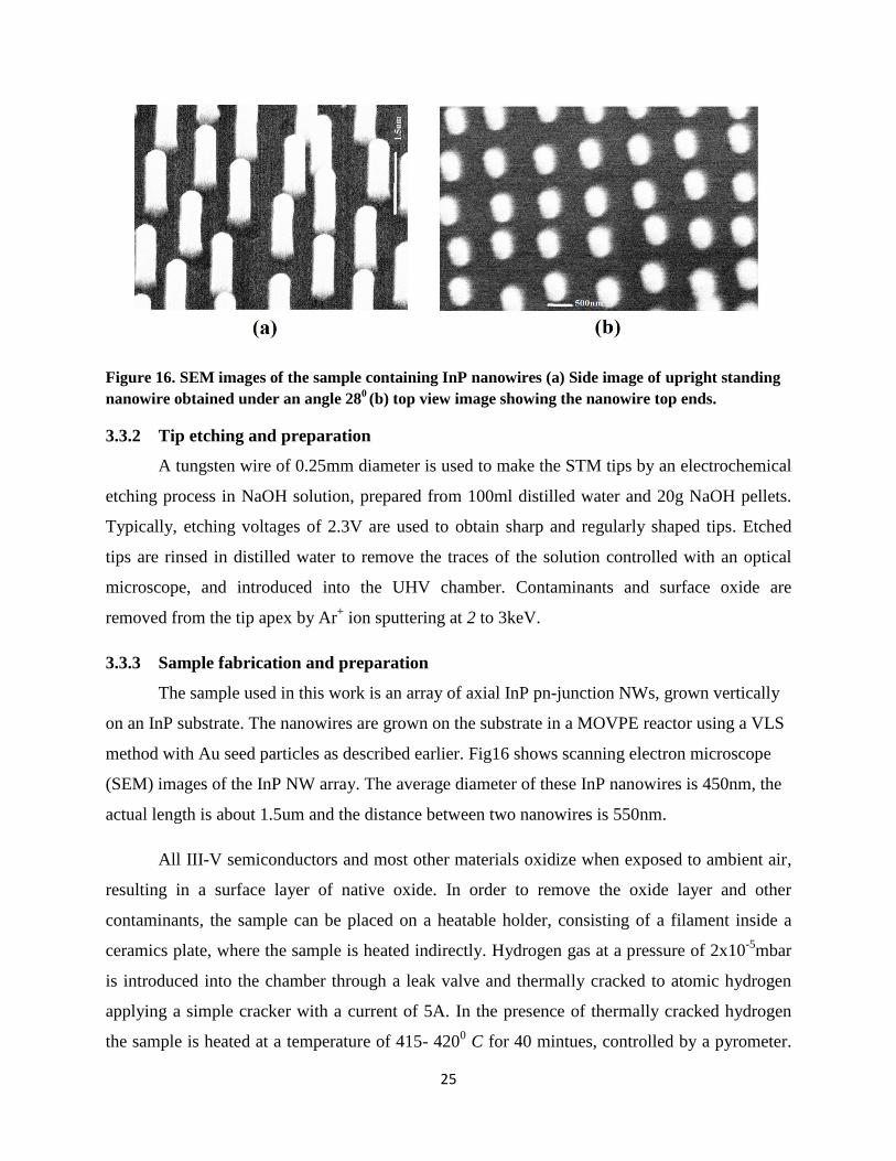
Scanning electron microscopy is used to produce images of the sample by scanning it
with an electron beam, as shown in Fig 16. In our work F-SEM JSM 6400F is used to measure
the length and diameter of the nanowires.
25
Figure 16. SEM images of the sample containing InP nanowires (a) Side image of upright standing
nanowire obtained under an angle 280 (b) top view image showing the nanowire top ends.
3.3.2 Tip etching and preparation
A tungsten wire of 0.25mm diameter is used to make the STM tips by an electrochemical
etching process in NaOH solution, prepared from 100ml distilled water and 20g NaOH pellets.
Typically, etching voltages of 2.3V are used to obtain sharp and regularly shaped tips. Etched
tips are rinsed in distilled water to remove the traces of the solution controlled with an optical
microscope, and introduced into the UHV chamber. Contaminants and surface oxide are
removed from the tip apex by Ar+ ion sputtering at 2 to 3keV.
3.3.3 Sample fabrication and preparation
The sample used in this work is an array of axial InP pn-junction NWs, grown vertically
on an InP substrate. The nanowires are grown on the substrate in a MOVPE reactor using a VLS
method with Au seed particles as described earlier. Fig16 shows scanning electron microscope
(SEM) images of the InP NW array. The average diameter of these InP nanowires is 450nm, the
actual length is about 1.5um and the distance between two nanowires is 550nm.
All III-V semiconductors and most other materials oxidize when exposed to ambient air,
resulting in a surface layer of native oxide. In order to remove the oxide layer and other
contaminants, the sample can be placed on a heatable holder, consisting of a filament inside a
ceramics plate, where the sample is heated indirectly. Hydrogen gas at a pressure of 2x10⁻⁵
mbar
is introduced into the chamber through a leak valve and thermally cracked to atomic hydrogen
applying a simple cracker with a current of 5A. In the presence of thermally cracked hydrogen
the sample is heated at a temperature of 415- 4200 C for 40 mintues, controlled by a pyrometer.

26
The atomic hydrogen interacts with the surface oxide and removes it from the surface. The
sample is then introduced again into the UHV STM chamber.
3.3.4 STM Tip –Sample approach for nanowire sample
After introducing the tip and sample, the next step is the tip-sample approach for starting
the STM imaging and finding the nanowires. Firstly, to bring the tip and sample very close, the
lateral and vertical movement of the tip is controlled by hand using simple electronic motors.
After this coarse approach and adjusting the electronics parameters at the electronics control unit,
the XPMPro Software is used for a further automatical tip-sample approach. In the case of a
nanowires sample, the height of standing nanowires is greater than the STM range along the z-
axis. The initial approach of the tip is not trivial. In the first tunneling contact the actual position
of the tip relative to the nanowire is not known. Therefore, the tip is retracted again until the
tunneling contact is lost.
3.3.5 STM imaging and formation of point contact
For STM imaging, the tip is now approached towards the sample surface in an iterative
procedure and is scanned, until we obtaine an image of the top end of several nanowires, as
sketched in Fig 17a. When several nanowires are found in the STM image, a point contact can be
established between the tip and one nanowire. Therefore, the STM tip is centered above one of
nanowire top end and further approached towards the nanowire, until a point contact is formed
between the tip and the nanowire as in Fig 17b. During this process the STM tip moves in steps,
called piezo steps. One piezo step is corresponding to the movement of the tip of about 5nm.
When the point contact is established, the tunneling current typically jumps to the saturation
level of STM electronics.

27
Figure 17. Sketch of the procedure for imaging, formation of point contact and conductitvity
measurement [28]
3.3.6 Electrical measurements
After establishing a point contact (Fig 17b), the electrical contact to the STM tip is
disconnected from the STM control unit and instead connected to the input of the external
current preamplifier as in Fig 17c. I-V curves of all nanowires are obtained via a Labview
program using a Stanford Research System SR830 Lock-In amplifier as programmable voltage
source and a Stanford Research System SR570 current preamplifier coupled with a HP34401A
Multimeter.

28
4. Results and Discussion
In this work I have measured the conductivity of individual pn-junction InP nanowires grown on
InP substrate, intended for solar cell application using the STM technique. I-V characteristics of
the nanowires are measured at room temperature. These measurments have been repeated with
many nanowires to obtain a statistical analysis of the sample, before and after cleaning it from a
native oxide layer.
4.1 Establishing a low resistive point contact
In Fig 18 we can see the typical I-V behavior of a nanowire in the voltage interval from
-0.5V (reverse bias) to +0.5V (forward bias) at room temperature during the formation of a low
resistive point contact between the sharp STM tip and the top end of the single nanowire.
Figure 18. I-V characteristics during the formation of a point contact between the STM tip and the
nanowire: At the initial contact (blue curve), the current is rather instable, resulting in a noisy I-V
curve. The current increases and stabilizes when the probe tip is further pushed into the nanowire
by small steps establishing a low resistive point contact .
-0.5 -0.4 -0.3 -0.2 -0.1 0 0.1 0.2 0.3 0.4 0.5-1
0
1
2
3
4
5
6x 10
-6
Voltage / V
Cur
rent
/ A
initial contact
5 steps
10 steps
29
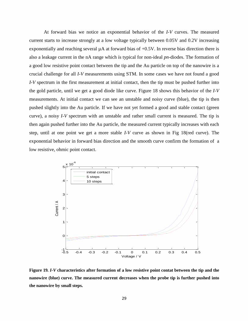
At forward bias we notice an exponential behavior of the I-V curves. The measured
current starts to increase strongly at a low voltage typically between 0.05V and 0.2V increasing
exponentially and reaching several µA at forward bias of +0.5V. In reverse bias direction there is
also a leakage current in the nA range which ís typical for non-ideal pn-diodes. The formation of
a good low resistive point contact between the tip and the Au particle on top of the nanowire is a
crucial challenge for all I-V measurements using STM. In some cases we have not found a good
I-V spectrum in the first measurement at initial contact, then the tip must be pushed further into
the gold particle, until we get a good diode like curve. Figure 18 shows this behavior of the I-V
measurements. At initial contact we can see an unstable and noisy curve (blue), the tip is then
pushed slightly into the Au particle. If we have not yet formed a good and stable contact (green
curve), a noisy I-V spectrum with an unstable and rather small current is measured. The tip is
then again pushed further into the Au particle, the measured current typically increases with each
step, until at one point we get a more stable I-V curve as shown in Fig 18(red curve). The
exponential behavior in forward bias direction and the smooth curve confirm the formation of a
low resistive, ohmic point contact.
Figure 19. I-V characteristics after formation of a low resistive point contat between the tip and the
nanowire (blue) curve. The measured current decreases when the probe tip is further pushed into
the nanowire by small steps.
-0.5 -0.4 -0.3 -0.2 -0.1 0 0.1 0.2 0.3 0.4 0.5-1
0
1
2
3
4
5x 10
-6
Voltage / V
Cur
rent
/ A
initial contact
5 steps
10 steps
30
Usually, we have found a good contact behavior already at the intial contact between the
tip and the nanowire, as shown in Figure 19 (blue curve). The InP nanowires are flexible in axial
direction, therefore further movement of the tip into the gold particle causes strain in the wire,
and the wire can even start to bend. The intrinsic conductivity of the pn-junction nanowire is
then changed. Now pushing the tip further into the Au particle causes a decreasing of the
measured current, as one can see in Figure 19 (green and red curve). For further data analysis, it
is essential to confirm the formation of an ohmic point contact. Only nanowires with stable and
reproducible I-V measurments are chosen for further analysis.
4.2 I-V characteristic of the InP pn-junction nanowires
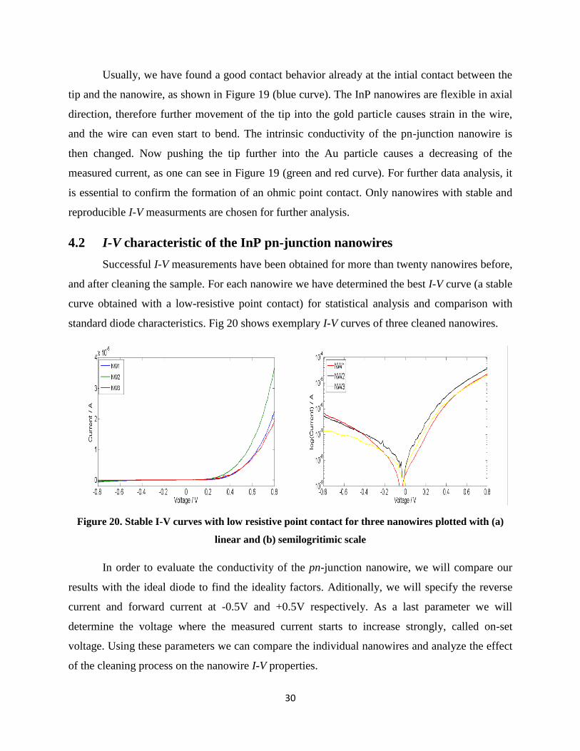
Successful I-V measurements have been obtained for more than twenty nanowires before,
and after cleaning the sample. For each nanowire we have determined the best I-V curve (a stable
curve obtained with a low-resistive point contact) for statistical analysis and comparison with
standard diode characteristics. Fig 20 shows exemplary I-V curves of three cleaned nanowires.
Figure 20. Stable I-V curves with low resistive point contact for three nanowires plotted with (a)
linear and (b) semilogritimic scale
In order to evaluate the conductivity of the pn-junction nanowire, we will compare our
results with the ideal diode to find the ideality factors. Aditionally, we will specify the reverse
current and forward current at -0.5V and +0.5V respectively. As a last parameter we will
determine the voltage where the measured current starts to increase strongly, called on-set
voltage. Using these parameters we can compare the individual nanowires and analyze the effect
of the cleaning process on the nanowire I-V properties.
31
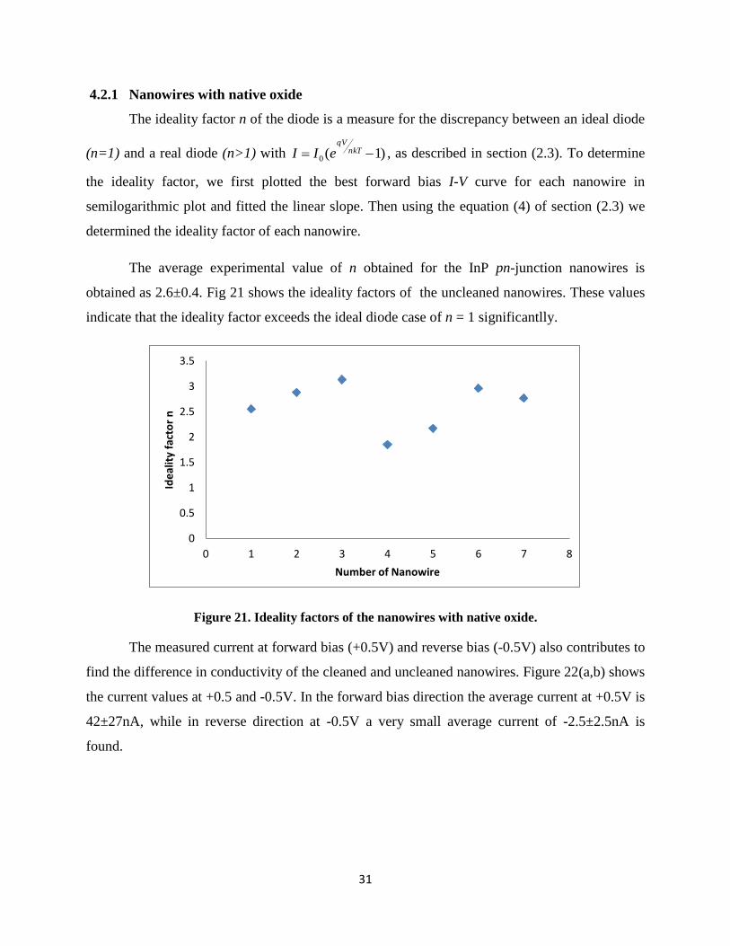
4.2.1 Nanowires with native oxide
The ideality factor n of the diode is a measure for the discrepancy between an ideal diode
(n=1) and a real diode (n>1) with )1(0 nkTqV
eII , as described in section (2.3). To determine
the ideality factor, we first plotted the best forward bias I-V curve for each nanowire in
semilogarithmic plot and fitted the linear slope. Then using the equation (4) of section (2.3) we
determined the ideality factor of each nanowire.
The average experimental value of n obtained for the InP pn-junction nanowires is
obtained as 2.6±0.4. Fig 21 shows the ideality factors of the uncleaned nanowires. These values
indicate that the ideality factor exceeds the ideal diode case of n = 1 significantlly.
Figure 21. Ideality factors of the nanowires with native oxide.
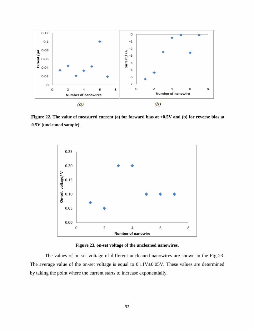
The measured current at forward bias (+0.5V) and reverse bias (-0.5V) also contributes to
find the difference in conductivity of the cleaned and uncleaned nanowires. Figure 22(a,b) shows
the current values at +0.5 and -0.5V. In the forward bias direction the average current at +0.5V is
42±27nA, while in reverse direction at -0.5V a very small average current of -2.5±2.5nA is
found.
0
0.5
1
1.5
2
2.5
3
3.5
0 1 2 3 4 5 6 7 8
Ide
alit
y fa
cto
r n
Number of Nanowire
32
Figure 22. The value of measured current (a) for forward bias at +0.5V and (b) for reverse bias at
-0.5V (uncleaned sample).
Figure 23. on-set voltage of the uncleaned nanowires.
The values of on-set voltage of different uncleaned nanowires are shown in the Fig 23.
The average value of the on-set voltage is equal to 0.11V±0.05V. These values are determined
by taking the point where the current starts to increase exponentially.
0.00
0.05
0.10
0.15
0.20
0.25
0 2 4 6 8
On
-se
t v
olt
age
/ V
Number of nanowire

33
4.2.2 Cleaned nanowires
New measurements have been done by repeating the same procedure after cleaning the
nanowire sample from the native oxide. The cleaning process is described earlier in section 3.3.
Figure 24. Ideality factors of the cleaned nanowires.
The ideality factors for the nanowires are shown in the Fig 24. The average value of n for
the cleaned sample is 2.5±0.1. This value is slightly smaller than for uncleaned sample, but the
ideality factors also after cleaning are still higher than the ideal diode value.
Figure 25. The value of measured current (a) for forward bias at +0.5Vand (b) for reverse bias at
-0.5V for the cleaned sample.
0
0.5
1
1.5
2
2.5
3
0 2 4 6 8 10
Ide
alit
y fa
cto
r n
Number of Nanowire
34
For the forward bias and reverse bias direction the measured values of the current at
+0.5V and -0.5V for the cleaned sample are given in Fig 25. The average current for forward
bias at +0.5V is 3.4±1.7µA. In the case of reverse bias the average current is -0.13±0.09µA at
-0.5V.
Figure 26. On-set voltage of the cleaned nanowires.
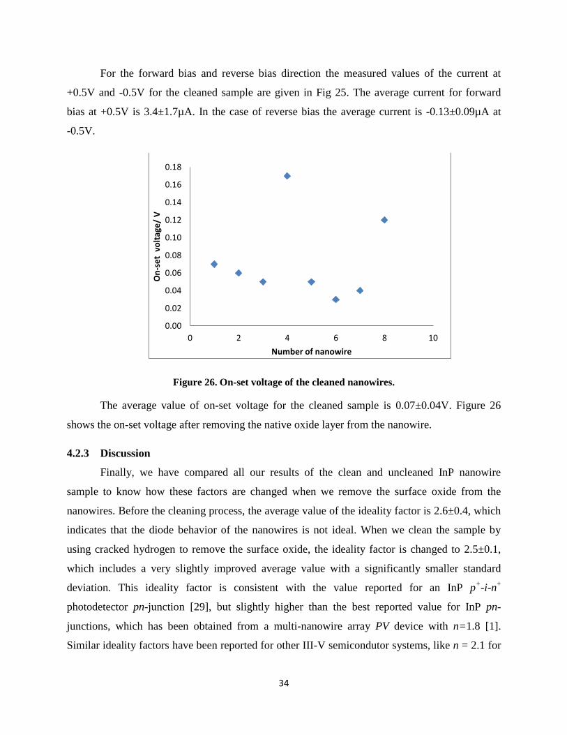
The average value of on-set voltage for the cleaned sample is 0.07±0.04V. Figure 26
shows the on-set voltage after removing the native oxide layer from the nanowire.
4.2.3 Discussion
Finally, we have compared all our results of the clean and uncleaned InP nanowire
sample to know how these factors are changed when we remove the surface oxide from the
nanowires. Before the cleaning process, the average value of the ideality factor is 2.6±0.4, which
indicates that the diode behavior of the nanowires is not ideal. When we clean the sample by
using cracked hydrogen to remove the surface oxide, the ideality factor is changed to 2.5±0.1,
which includes a very slightly improved average value with a significantly smaller standard
deviation. This ideality factor is consistent with the value reported for an InP p+-i-n
+
photodetector pn-junction [29], but slightly higher than the best reported value for InP pn-
junctions, which has been obtained from a multi-nanowire array PV device with n=1.8 [1].
Similar ideality factors have been reported for other III-V semicondutor systems, like n = 2.1 for
0.00
0.02
0.04
0.06
0.08
0.10
0.12
0.14
0.16
0.18
0 2 4 6 8 10
On
-se
t v
olt
age
/ V
Number of nanowire
35
GaInP nanowire p-i-n junctions [30], and n=3 for GaAs pn-junctions [31]. This comparison to
the literature values shows that the diode behavior of our nanowires is equally good as that of
other state-of-the-art nanowire pn-junctions. However, the ideality factors both with and without
native oxide layer are still significantly higher than 1.0, thus exceeding the ideal theoretical value
by far. Higher values of ideality factors suggest that ohmic losses must be considered, which
reduce the net current through the device. Also other possible reasons of high ideality factors
should be considered, such as the serial resistance due to non-perfect interfaces, defects at the
nanowire surface or within the nanowire crystalline structure, or a non-perfect pn-interface itself.
Other important diode parameters are the forward and reverse current. The average value
of the current at +0.5V forward bias for uncleaned nanowires is 42nA, while for cleaned
nanowires it amounts to 3.4uA which is nearly a factor of hundred higher. This shows that the
conductivity of the InP increases dramatically when we remove the surface oxide from the
nanowires. Similarly, in reverse bias direction the average current at -0.5V is -2.5nA for
uncleaned nanowires, while after cleaning it increases by a factor of 50 to -0.13 µA.
If a perfect diode was available, zero current would be measured in reverse direction and
higher current in forward direction. But it is found for every real pn-junction, that a small amount
of current flows in the reverse bias direction as a result of the minority carriers in the
semiconductor. The level of leakage current is dependent upon the type of semiconductor. It
should be noted that in our experiment also the reverse current is significantly increased when
we remove the surface oxide from the sample. This might be due to unpinning of the Fermi level
when the surface oxide is removed, as discussed later on.
When we compare all our results for both cleaned and uncleaned nanowires, we notice
that all the above parameters changed when we heated the sample in the presence of hydrogen
atoms to remove the surface oxide layer from the InP nanowires surfaces. The measured current
value of the individual nanowire changes in both forward and reverse bias direction, as well as
the on-set voltage and ideality factor. In the following, several possible reasons for this
significant changes are discussed. We start with how the surface oxide can influence the
electrical properties of the nanowire. It is reported [32] that InP oxides pin the Fermi level close
to the conduction band in n-type side and valence band in p-side and cause band bending. In Ref
[32], Hjort et al. have used the same method of atomic hydrogen-assisted annealing to remove

36
the native oxide from InP nanowire surfaces as we have used here. They investigated the
influence of an oxide layer on the electrical nanowire properties by using a combination of XPS,
XPEEM, LEEM, STM and STS techniques. Instaed of studying upright standing nanowires, their
nanowires were firstly broken off from the substrate and then investigated from the side. The
removal of oxide from the InP nanowire surface leads to unpinning of the Fermi level and
reduces the band bending. Since the oxide induced band bending is very strong, it also severely
affects the interior of the nanowire so that the conductivity of the InP nanowires is reduced. This
effect of Fermi-level pinning due to surface oxides explains the relatively poor conductivity of
the uncleaned nanowires in our work, which increases over two orders of magnitude after
cleaning the nanowires.
Defects at the nanowire surface can act as electron/hole traps, affecting the electrical
properties of the material and the conductivity of the nanowire There are other possibilities
which can explain the observed change of conductivity parameters and increased conductivity,
such as the dopant concentration in both p-type and n-type side, impurities and defects in the
depletion region, and an imperfect interface between the Au-particle and nanowire surface. Upon
heating and removing the surface oxide from the nanowires these defects (surface, and
depeletion region) can be removed. Also imperfect interfaces which causes the serial resistance
can be improved. Another possible reason are ionic charges on the nanowire surface which
induce an image charge inside the nanowire surface. A depletion layer is formed at the surface
and gives rise to surface leakage current and affects the conductivity.

37
5. Conclusion and outlook
5.1 Conclusion
We have studied the electrical properties of InP pn-junction nanowires, using scanning
tunneling microscopy technique. These I-V characteristics have been measured with and without
a native oxide layer on the nanowire surface.
The scanning tunneling microscopy technique is particularly successful to make a low
resistive point contact between the probe tip and the top end of the individual nanowire. A
speciality of the used setup is the possibility to integrate an external setup (voltage source, and
current amplifier) into the STM system.
The I-V characeristcs for the cleaned and uncleaned InP nanowires sample were
measured for room temperature in ultrahigh vaccum conditions. We have evaluated our results in
regard to the ideal diode characteristics, and we have compared I-V properties of uncleaned and
cleaned nanowires. For this results we have investigated specific parameters, such as ideality
factor, reverse and forward current at +0.5V and -0.5V, and the on-set voltage.
When we have compared our results with the ideal diode behavior, we found the average
ideality factor 2.5 to 2.6 for both cleaned and uncleaned nanowires which are significantly
exceeding the ideal value (n=1.0) although they are in the range of best reported pn-junction
nanowires. All investigated parameters, such as ideality factor, on-set voltage, reverse and
forward current at +5.0V and -5.0 V are changed when we clean the sample. We relate this
behavior to the fact that the oxide layer on the nanowire surface can pin the surface Fermi energy
level. The pinning of surface Fermi level causes band bending and reduces the conductivity.
Heating the sample during cleaning process also reduces defects at the surface that can act as
electron/hole traps and thus increases the conductivity of the device.
5.2 Outlook
Results of this projects are relevant for the NWs pn-junction processing. In this project
we have used normal LED and laser light, but we have not found an affect of light on the InP pn-
junction nanowire I-V curves. There are few obvious improvements to the apparatus which
would give it capability for producing more accurate and meaningful results.

38
Replacing the laser with a more powerful laser and good optical system would improve
the effect of light on the sample and our results
A more robust and powerful laser should be fixed inside the ultrahigh vaccum chamber of
the STM, whose angle could be easily adjusted to incident laser light on the sample
easily.
One important advantage of a nanowire solar cell is that III-V semiconductor nanowires can
be integrated or grown on many other substrates. In the future, it would therefore be important to
study InP nanowires grown on cheap and industrially relevant silicon substrate.

39
Bibliography
[1] M. T. Borgstrom, J. Wallentin, M. Heurlin, S. Falt , P. Wickert, J. Leene, M. H. Magnusson, K. Deppert
and L. Samuelson, "Nanowires With Promise for Photovoltaics," IEEE, vol. 17, pp. 1050-1061, 2011.
[2] G. Goncher and R. Solanki, "Semiconductor Nanowire Photovoltaics," Society of Photo-Optical
Instrumentation Engineers (SPIE) Conference Series, vol. 7047, 2008.
[3] M. A. Green, "The path to 25% silicon solar cell effeciency:History of silicon solar cell evolution,"
Progress in Photovoltaics: Research and Applications, vol. 17, no. 3, pp. 183-189, 2009.
[4] H. Spanggaard and F. C. Kerbs, "A brief history of the development of organic and polymeric
photovoltaics," Solar Energy Material and Solar Cells, vol. 83, pp. 125-146, 2004.
[5] "http://en.wikipedia.org/wiki/Thin_film_solar_cell#cite_note-renew-7," [Online].
[6] B. Tian, T. J. Kempa and C. M. Lieber, "Single Nanowire Photovoltaics," Chemical Society Reviews,
vol. 38, pp. 16-24, 2008.
[7] R. Yan, D. Garges and P. Yang, "Nanowire photonics," Nature photonics, vol. 3, pp. 569-576, 2009.
[8] E. C. Garnett , M. L. Brongersma, Y. Cui and M. D. McGehee, "Nanowire Solar Cells," Annual Review
of Materials Research, vol. 41, pp. 269-295, 2011.
[9] Y. Qu and X. Duan, "One-dimensional homogeneous and heterogeneous nanowires for solar energy
conversion," Material Chemistry, vol. 22, pp. 16171-16181, 2012.
[10] J. Wallentin, N. Anttu, D. Asoli, M. Huffman, I. Aberg, M. H. Magnusson, G. Siefer, P. F. Kailuweit, F.
Dimroth, B. Witzigmann, H. Q. Xu, L. Samuelson, K. Deppert and M. T. Borgstrom, "InP Nanowire
Array Solar Cells Achieving 13.8% Efficiency by Exceeding the Ray Optics Limit," Sciencexpress, 2013.
[11] Z. Zhang, K. Yao, Y. Liu, C. Jin, X. Liang, Q. Chen and L.-M. Peng, "Quantitative Analysis of Current–
Voltage Characteristics of Semiconducting Nanowires: Decoupling of Contact Effects," Advanced
Functional Material, vol. 17, p. 2478, 2007.
[12] O. Mah, "Fundamentals of Photovoltaics Materials," 1998.
[13] S. M. Sze, Physics of Semiconductor Devices, John Wiley and Sons, 1969.
[14] C. Kittel and C. Kittel, Introduction to Solid State physics, John Wiley and Sons, 1996.
40
[15] D. A. Neamen, Semicondutor Physics and Devices, Elizabeth A. jones, 2003.
[16] G. Parker, Introductory Semiconductor Device Physics, Simon & Schuster International Group, 1994.
[17] M. S. Dresselhaus, Y.-M. Lin, O. Rabin, M. R. Black, J. Kong and G. Dresselhaus, "Nanowires," in
Handbook of Nanotechnology, Springer, 2010.
[18] K. Dick, "Epitaxial Growth and Design of Nanowires and Complex Nanostructure," Lund, 2007.
[19] M. T. Borgstrom, E. Norberg, P. Wickert, H. A. Nilsson, J. Tragardh and K. Dick, "Precursor evalution
for in-situ InP nanowire doping," Nanotechnology, 2008.
[20] T. Martensson, P. Carlberg, M. Borgstrom, L. Montelius, W. Seifert and L. Samuelson, "Nanowire
Arrays Defined by Nanoimprint Lithography," Nano Letters, vol. 4, pp. 699-702, 2004.
[21] M. Hjort, "Surface studies of III-V nanowires," Lund University, 2012.
[22] J. Bolinsson, "The Crystal Structure of III-V Semiconductor Nanowires:," Lund university, 2010.
[23] J. Wallentin and M. T. Borgstrom, "Doping of semiconductor nanowires," material Research Society,
vol. 26, pp. 2142-2156, 2011.
[24] C. Honsberg and S. Bowden, "PV EDUCATION.ORG," PV education, 2012. [Online].
[25] B. V. Zeghbroeck, "Principles of Semiconductor Devices," University of Colorado, 2011. [Online].
Available: http://ecee.colorado.edu/~bart/book/book/chapter4/ch4_4.htm.
[26] S. Peter, "http://www.stallinga.org/ElectricalCharacterization/2terminal/index.html," [Online].
[27] Sutter.P, "Scanning Tunneling Microscopy in Surface Science," in Science of Microscopy, Springer,
2007.
[28] R. Timm, D. Engberg, A. Fian, O. Persson, J. Wallentin, M. Borgstrom, L. Samuelson and A.
Mikkelsen, "Conductivity Measurment on Individual as-grown Nanowires using a Scanning
Tunneling Microscope," Lund.
[29] H. Patetersson, I. Zubritskaya, N. T. Nghia, J. Wallentin, M. T. Borgstrom, K. Storm, L. Landin, P.
Wickert, F. Capasso and L. Samuelson, "Electrical and optical properties of InP nanowire ensemble
p+-i-n+ photodetectors," Nanotechnology, vol. 23, 2012.
[30] J. Wallentin, L. B. Poncela, A. M. Jansson, K. Mergenthaler, M. Ek, D. Jacobsson, L. R. Wallenberg, K.
Deppert, L. Samuelson, D. Hessman and M. T. Borgstrom, "Single GaInP nanowire p-i-n junctions
near the direct and indirect bandgap crossover point," Applied Physics letters, vol. 100, p. 251103.

41
[31] A. Lysov, M. Offer, C. Gutsche, I. Regolin, S. Topaloglu, M. Geller, W. Prost and F.-J. Tegude, "Optical
properties of heavily doped GaAs nanowires and electroluminescent nanowire structure,"
Nanotechnology, vol. 22, 2011.
[32] M. Hjort , J. Wallentin, R. Timm, A. A. Zakharov, U. Hakanson, J. N. Andersen, E. Lundgren, L.
Samuelson, M. T. Borgstrom and A. Mikkelsen, "Surface Chemistry, Structure, and Electronic
Properties from Microns to the Atomic Scale of Axially doped Semiconductor nanowires," American
Chemical Society, vol. 6, pp. 9679-9689, 2012.
[33] I. Saj and D. Saj, "Nanowire-based InP Solar cell Material," Halmstad, 2012.
42
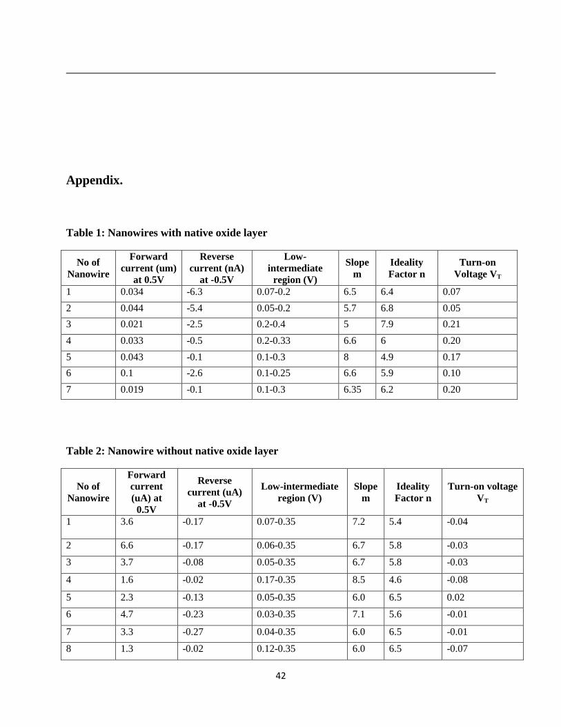
Appendix.
Table 1: Nanowires with native oxide layer
No of
Nanowire
Forward
current (um)
at 0.5V
Reverse
current (nA)
at -0.5V
Low-
intermediate
region (V)
Slope
m
Ideality
Factor n
Turn-on
Voltage VT
1 0.034 -6.3 0.07-0.2 6.5 6.4 0.07
2 0.044 -5.4 0.05-0.2 5.7 6.8 0.05
3 0.021 -2.5 0.2-0.4 5 7.9 0.21
4 0.033 -0.5 0.2-0.33 6.6 6 0.20
5 0.043 -0.1 0.1-0.3 8 4.9 0.17
6 0.1 -2.6 0.1-0.25 6.6 5.9 0.10
7 0.019 -0.1 0.1-0.3 6.35 6.2 0.20
Table 2: Nanowire without native oxide layer
No of
Nanowire
Forward
current
(uA) at
0.5V
Reverse
current (uA)
at -0.5V
Low-intermediate
region (V)
Slope
m
Ideality
Factor n
Turn-on voltage
VT
1 3.6 -0.17 0.07-0.35 7.2 5.4 -0.04
2 6.6 -0.17 0.06-0.35 6.7 5.8 -0.03
3 3.7 -0.08 0.05-0.35 6.7 5.8 -0.03
4 1.6 -0.02 0.17-0.35 8.5 4.6 -0.08
5 2.3 -0.13 0.05-0.35 6.0 6.5 0.02
6 4.7 -0.23 0.03-0.35 7.1 5.6 -0.01
7 3.3 -0.27 0.04-0.35 6.0 6.5 -0.01
8 1.3 -0.02 0.12-0.35 6.0 6.5 -0.07

43