thin film technology filter design · pdf filerev 9.0 august 2011 thin film technology filter...
TRANSCRIPT

Rev 9.0 August 2011 Thin Film Technology Filter Design Guide Page 1 of 36
Thin Film Technology Filter
Design Guide
Rev 9.0 August 2011 Thin Film Technology Filter Design Guide Page 2 of 36
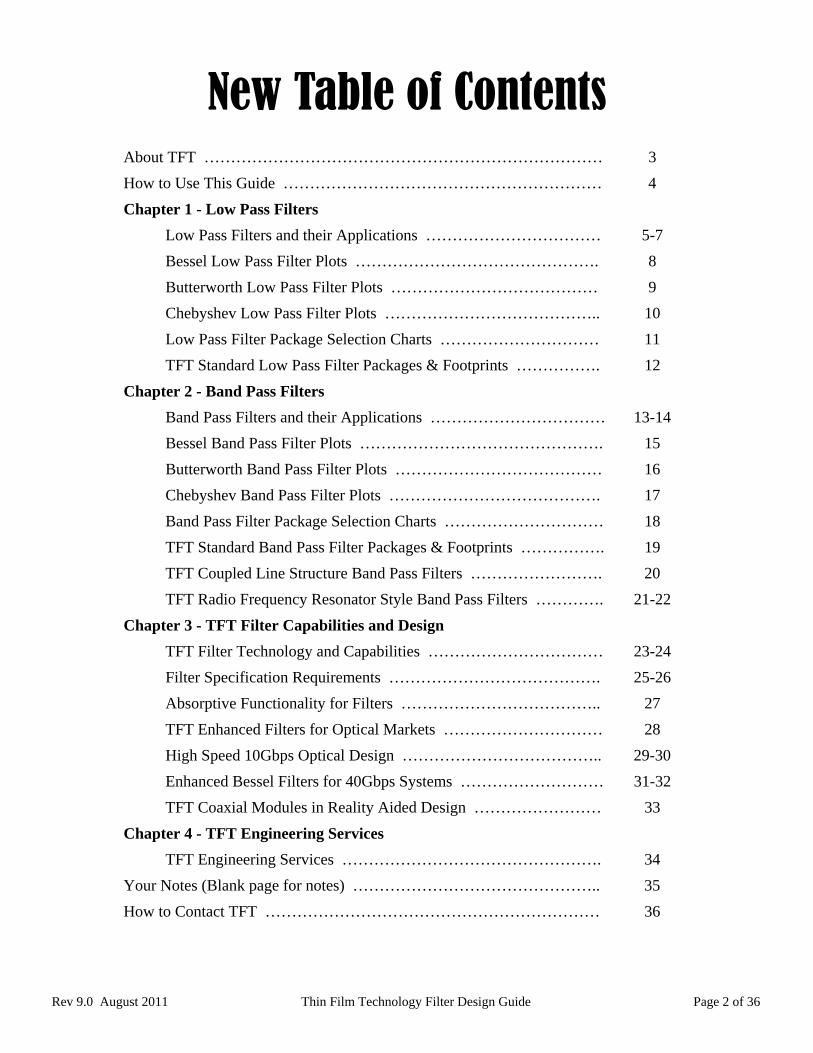
New Table of Contents
About TFT ………………………………………………………………… 3
How to Use This Guide …………………………………………………… 4
Chapter 1 - Low Pass Filters
Low Pass Filters and their Applications …………………………… 5-7
Bessel Low Pass Filter Plots ………………………………………. 8
Butterworth Low Pass Filter Plots ………………………………… 9
Chebyshev Low Pass Filter Plots ………………………………….. 10
Low Pass Filter Package Selection Charts ………………………… 11
TFT Standard Low Pass Filter Packages & Footprints ……………. 12
Chapter 2 - Band Pass Filters
Band Pass Filters and their Applications …………………………… 13-14
Bessel Band Pass Filter Plots ………………………………………. 15
Butterworth Band Pass Filter Plots ………………………………… 16
Chebyshev Band Pass Filter Plots …………………………………. 17
Band Pass Filter Package Selection Charts ………………………… 18
TFT Standard Band Pass Filter Packages & Footprints ……………. 19
TFT Coupled Line Structure Band Pass Filters ……………………. 20
TFT Radio Frequency Resonator Style Band Pass Filters …………. 21-22
Chapter 3 - TFT Filter Capabilities and Design
TFT Filter Technology and Capabilities …………………………… 23-24
Filter Specification Requirements …………………………………. 25-26
Absorptive Functionality for Filters ……………………………….. 27
TFT Enhanced Filters for Optical Markets ………………………… 28
High Speed 10Gbps Optical Design ……………………………….. 29-30
Enhanced Bessel Filters for 40Gbps Systems ……………………… 31-32
TFT Coaxial Modules in Reality Aided Design …………………… 33
Chapter 4 - TFT Engineering Services
TFT Engineering Services …………………………………………. 34
Your Notes (Blank page for notes) ……………………………………….. 35
How to Contact TFT ……………………………………………………… 36

Rev 9.0 August 2011 Thin Film Technology Filter Design Guide Page 3 of 36
About Thin Film Technology Corp.
Thin Film Technology Corporation is an electronic component manufacturer specializing in
thin film technology. Established in 1979 in North Mankato, Minnesota, for over 30 years,
Thin Film Technology has used thin film as the springboard to devise innovative
component technologies to the high technology markets.
Thin film processing itself is a skilled art, and in combination with advanced manufacturing
technologies, the creation of product technologies that were once only dreams can be
achieved. Thin Film Technology maintains the view that thin film components do not need
to be expensive. Through common sense manufacturing methods, affordable, high
performance products can be obtained. Against this unique approach, Thin Film Technology
sees each customer need as a challenge, one to provide only the finest in affordable
performance thin film products.
The art of combination. . . the essence of Thin Film Technology. Since 1980 Thin Film
Technology has been designing and manufacturing thin film components. From our
ISO9001 and ISO14000 registered factory, quality products serving the computer, test
equipment, telecommunication, medical, automotive and other electronic markets are
shipped worldwide.

Rev 9.0 August 2011 Thin Film Technology Filter Design Guide Page 4 of 36
Purpose:
The purpose of this filter selection guide is to
outline predetermined filter functional responses
along with frequency scaling and packaging
requirements to provide a method of selection.
Basic filters have multitudes of applications and
uses. There are also inherent merits and trade-
offs to different functional elements. A good
amplitude selective filter such as a butterworth
has phase dispersion that influences overshoot in
the time domain. On the other hand, the flat delay
response of the bessel function exhibits a gradual
amplitude loss slope that contributes to jitter in
the time domain. Along with selecting basic filter
function attributes, certain attributes are
increased by the order of the filter. For example,
increasing the order of a butterworth filter
increases its selectivity. Increased filter orders are
accomplished by adding resonator elements that
also increase physical size and material costs.
The frequency at which a filter is designated is
normally its 3dB roll-off point. This frequency is
inversely proportional to size. This means lower
frequencies are prohibitive to certain
technologies based on physical size. This guide
outlines the typical sizes associated with
frequency scaling.
How To Use:
1. The basic filter functions are presented first for
general response comparisons. Once you
decide on the type of response you are
interested in applying, more detailed responses
are presented for comparison of attributes
versus frequency for amplitude, phase, and
time domain (low pass).
2. Deciding on the order of the filter required, the
phase dispersion and amplitude responses can
be scaled from the nominal 1GHz chart to give
a good idea of the response at any frequency.
3. Once the type, function, order, and frequency
of the required filter are obtained, the package
requirements are grouped by charts that
display element area versus frequency for each
type of filter. These charts display separate
slopes for each order of the specified filter
type, and the area available in each package
type.
4. The package types and dimensions are
outlined after the package selection charts on
page 17.
How to Use This Guide
Rev 9.0 August 2011 Thin Film Technology Filter Design Guide Page 5 of 36
Introduction
Filters are essential to the operation of most
electronic circuits. In circuit theory, a filter is an
electrical network that alters the amplitude and/or
phase characteristics of a signal with respect to
frequency. Ideally, a filter will not add new
frequencies to the input signal, nor will it change
the component frequencies of that signal, but it
will change the relative amplitudes of the various
frequency components and/or their phase
relationships.
Filters are often used in electronic
systems to emphasize signals in certain frequency
ranges and reject signals in other frequency
ranges. To correctly specify a filter’s
characteristics one has to understand and specify
the four corners of the filter’s transfer function’s
plot. Without the four corners one will fall of the
edge of the world. One of the four corners would
be the signal magnitude of lowest interest of
frequency. The second corner would be the –3dB
cutoff frequency point of the signal magnitude.
The third corner would be the rejection frequency
and rejection magnitude of the signal and the
fourth and last corner would be the out of band
rejection point of maximum interested frequency.
Without specifying these four corners a filter’s
characteristics cannot be demonstrated.
Describing all the applications of a filter in
any electronics system is beyond this application
note. Brief descriptions of several filter
applications are discussed in the following.
Desired Signal Selection:
One of the most common applications of
the filters is to select wanted signal component
from the available frequency band and reject
unwanted signal component from the frequency
band. The addition of appropriate filters in the
system will guard the interested signal
component against any interference across
adjacent signals. It not only distinguishes desired
signal from other frequency components, but also
reduces noise, which is added with the desired
signal; and eliminates cross talks in between
signals. The consequences of inadequate filtering
translate into cross talk, signal drop out, noisy
signal, and even complete transmission
interruption. These phenomenon result in loss of
data and interrupted network connections among
users. Using correct filters can help maintain
signal integrity as well combat the difficulty in
transmitting and receiving a clear signal.
Duo-binary Signal Generation for Optical
Communication:
In the optical communication domain,
among several modulation formats, Duo-binary
modulation format is a popular choice among
fiber-optic communication system engineers. It is
a spectrally compressed modulation format,
which achieves robust chromatic dispersion
tolerance while utilizing standard direct detection
optical receivers. In its most common
implementation, a Duo-binary signal is created
using an encoder, an electrical driver amplifier, a
Low Pass Filters and their Applications

Rev 9.0 August 2011 Thin Film Technology Filter Design Guide Page 6 of 36
Mach-Zehnder modulator, and an electrical filter
with a –3dB cutoff around 25-35% of data rate.
Without the filter, three level Duo-binary signal
creation would be impossible. The key point
regarding the optical Duo-binary format is that
linear phase response is needed in the electrical
components in order to create the most robust
transmitted eye diagram possible. This kind of
linear phase response is achieved by using a Bessel
Thompson filter.
Bit pattern dependent distortion minimization
in Digital Communication:
In modern digital communications systems,
system engineers must be aware of the impact both
the magnitude and phase response of the associated
components and transmission lines will have on the
quality of the received bits. To minimize the bit
pattern distortions phenomenon in the transmitter
and receiver, a flat group delay filter can be
employed. Using a flat group delay filter helps all
of the frequency components comprising the
transmitted pulses pass through the filter with the
same time delay. It is necessary to use filters with
flat group delay in order to achieve the highest eye
quality in terms of overshoot/undershoot and eye
symmetry. Bessel-Thompson (BT) filters can be
used to filter digital signals in both transmitter and
receiver applications because of their “maximally
flat” group delay (i.e. highest linear phase)
characteristics. BT filters achieve a significantly
flatter group delay response at the expense of
decreased stop band rejection.
Jitter elimination and overshoot ringing
elimination:
When working in the time domain,
designers face the presence of undesirable
perturbations on a pulse signal, such as precursors,
overshoot, and signal ringing. These perturbations
extend well beyond the rise time interval and create
uncertainty in the actual value of the pulse for a
much longer duration. As the bandwidth increases,
the signal experiences very fast rise time and fall
time. This higher speed causes timing jitter
resulting in a smaller signal eye opening. Faster
signals also take a longer time to settle down to the
final values and creates overshoot ringing, which
also helps reducing signal eye opening. These
phenomenon eventually reduce integrity of the
signal.
One effective way to combat these
undesired events is to use a optimum Gaussian low
pass filter. With Gaussian wave shapes, pulse
signals rise and fall smoothly and then rapidly
settle to their final bit values. Also with filter
frequency response, signals bandwidth is reduced,
which eventually slows down the rise and fall time.
Slower rise and fall time reduces the timing jitter in
the signal. All oscilloscope manufacturers strive to
make their oscilloscopes with responses
approximating to the Gaussian filter shape.
Inter-Symbol Interference (ISI) minimization
Another important phenomenon that system
engineers needs to worry about is Inter Symbol
Interference (ISI). Transmitting rectangular signal
pulse through a limited-bandwidth channel distorts
the pulse by smearing it, where the pulse gets
stretched out in time. Moreover, due to the nature
of multipath propagation, the transmitted signal

Rev 9.0 August 2011 Thin Film Technology Filter Design Guide Page 7 of 36
experiences delay spread, resulting in one symbol
spreading into subsequent symbols. This spreading
and smearing of the symbols carries the energy
from one symbol to the next ones. This interference
between adjacent symbols is called inter-symbol
interference (ISI). Presence of ISI in the received
signal increases the probability of signals being
interpreted incorrectly. Communication system
designs for both wired and wireless nearly always
need to incorporate some way of controlling ISI.
The addition of a low pass filter in the receiver path
can help remove these defects. Raised cosine low
pass filters are usually employed to reduce ISI
(Inter Symbol Interference) in between bit pulse. In
certain digital telecom systems, such as SDH,
SONET, and Fiber Channel, system specifications
mandate the use of low pass filters with –3 dB
cutoff frequencies of 0.75 of the bit rate.
Aliasing Reduction
While sampling data, system engineers
must pay attention to the sampling rate. Sample
rates must be greater than or equal to two times the
highest frequency component in the input signal.
When this rule is violated, unwanted or undesirable
signals appear in the frequency band of interest.
This is called "aliasing." This aliasing phenomenon
due to unwanted, spurious out of band signals can
seriously endanger the performance of successful
signal transmission. Aliasing can be reduced and
eliminated by using anti-aliasing filters. Anti-
aliasing filters provide a cut off frequency that
removes unwanted signals (aliasing component) or
at least attenuates them to the point that they do not
adversely affect the system performance. Optimally
designed low pass filters with high ‘Q’ value can
be used as anti-aliasing filters to reduce the aliasing
occurrence.
Out of Band Reflections elimination
Another degradation factor for ultra high
speed signal transmission is the reflections that
take place outside the desired bands. Undesired
interference and increased jitter can occur due to
the out of band reflections. Absorptive low pass
filters can eliminate out of band reflections. Using
absorptive low pass filters, designers can achieve
good VSWR even outside the interested frequency
bands. Absorptive filters provide superior
impedance matching in both the pass band and stop
band. These absorb out of band reflections without
the need for additional fixed attenuators.
Conclusion
Several applications have been discussed in
this chapter. The main application for low pass
filters is to filter out undesired signal components
from the band. This would clear out the signal from
noise, cross talk, jitter and other undesired
phenomenon. Other important applications
including application in time domain as well as
digital domain has also been discussed. Filters are
one of the most necessary components in any sort
of signal transmission. Without filters’ presence in
the subsystem and system level, no data
transmission would be possible.

Rev 9.0 August 2011 Thin Film Technology Filter Design Guide Page 8 of 36
Bessel Low Pass Filter Plots

Rev 9.0 August 2011 Thin Film Technology Filter Design Guide Page 9 of 36
Butterworth Low Pass Filter Plots

Rev 9.0 August 2011 Thin Film Technology Filter Design Guide Page 10 of
Chebychev Low Pass Filter Plots
Rev 9.0 August 2011 Thin Film Technology Filter Design Guide Page 11 of
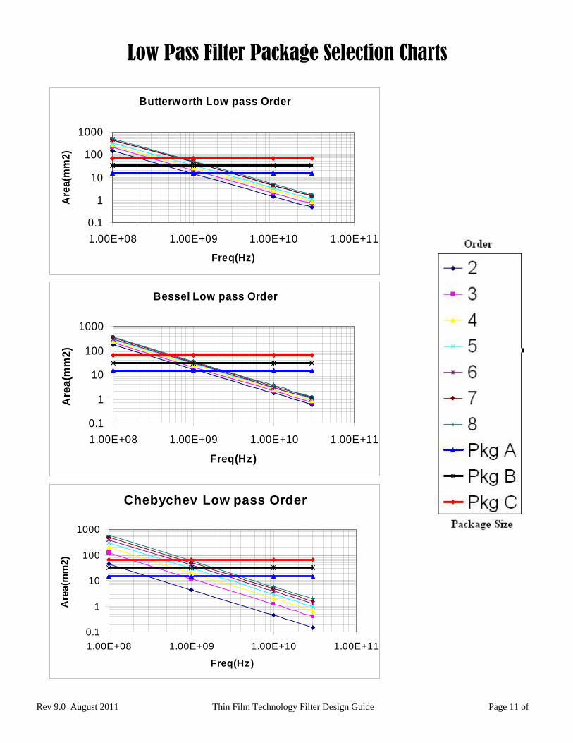
Low Pass Filter Package Selection Charts
Butterworth Low pass Order
0.1
1
10
100
1000
1.00E+08 1.00E+09 1.00E+10 1.00E+11
Freq(Hz)
Are
a(m
m2)
Bessel Low pass Order
0.1
1
10
100
1000
1.00E+08 1.00E+09 1.00E+10 1.00E+11
Freq(Hz)
Are
a(m
m2
)
Chebychev Low pass Order
0.1
1
10
100
1000
1.00E+08 1.00E+09 1.00E+10 1.00E+11
Freq(Hz)
Are
a(m
m2
)

Rev 9.0 August 2011 Thin Film Technology Filter Design Guide Page 12 of
TFT Standard Low Pass Filter Packages & Footprints
Package A (7.1 x 2.0mm—6 pin BGA)
Package B (6.35 x 5.08mm—6 pin BGA)
Package C (10.16 x 6.35mm—14 pin BGA)
Contact factory for DXF output of this footprint
Contact factory for DXF output of this footprint
Contact factory for proper footprint and DXF output.

Rev 9.0 August 2011 Thin Film Technology Filter Design Guide Page 13 of
Introduction
Band Pass Filters are essential to almost all
signal processing circuits. They are used in
electronic systems to pass certain components of
the signals entire spectrum. They pass certain
desired frequencies of the signal spectrum, while
rejecting and attenuating the undesired frequency
components of the signal spectrum. An ideal
band pass filter should have a completely flat
pass band and should completely attenuate all
frequency spectrums outside of the pass band.
However, in practical terms, filters cannot
completely attenuate all frequencies outside the
desired frequency range. There is region outside
of the intended pass band where frequencies are
attenuated, but not rejected. This is known as the
roll-off frequency. Generally, filter designs
attempt to make the roll-off as narrow as
possible, thus allowing the filter to perform as
close as possible to its intended design. The
cutoff frequency of the band pass filter is the
boundary where the undesired frequency
component is attenuated. It is the edge of the
filter frequency response range. The bandwidth
of the filter is the difference between the upper
and lower cutoff frequencies.
Describing all the applications of the Band
pass filter is beyond the scope of this application
note. Brief descriptions of several filter
applications are discussed in the following.
Desired Signal Selection:
The most important applications of the Band
Pass filters is to pass the desired signal
components from the available frequency
spectrum and reject unwanted signal components.
In a data transmission system, desired data is
embedded in the specific frequency. Band pass
filters can be used to successfully collect the data
from the entire frequency spectrum. The filter is
used to pass only the desired portion of the
spectrum, where the data is embedded; and to
attenuate the other frequencies. To the receivers
point of view, the frequency spectrum that does
not have the embedded data is undesired
information. Thus, by running the signal through
the appropriate filter, the undesired portion of the
frequency is rejected, leaving only the frequency
where data is embedded.
The consequences of inadequate filtering
translate into cross talk, signal drop out, noisy
signals, and even complete transmission
interruption. These phenomenon result in loss of
data and interrupted network connections among
users. Using the correct filters can help maintain
the signal integrity as well as to combat the
difficulty in transmitting and receiving a clear
signal.
Reducing Inter Symbol Interference (ISI)
Appropriate filter placement in the system
will guard the desired signal component against
any interference across adjacent signals. The
filter will attenuate all of the frequency
components, including adjacent signals, while
accepting the desired signal portions. As a result,
it will diminish the vast majority of the
interference due to adjacent signals. Band pass
filters will also help to bring Inter Modulation
Distortion (IMD) and Cross Modulation
Band Pass Filters and their Applications

Rev 9.0 August 2011 Thin Film Technology Filter Design Guide Page 14 of
Distortion (CMD) problems due to modulation
under control
Cross Talk Reduction:
In signal transmission, “Cross Talk” refers
to the phenomenon where the transmitted signal in
one channel or frequency creates and undesired
effect in another channel or frequency. It is due to
the coupling of one circuit to another. This
phenomenon takes place where the signal content
leaks (bleeds) from one channel to the other
adjacent channels. Cross talk is often described as
co-channel interference and adjacent channel
interference. Appropriate band pass filtering
around the desired frequency stops the other
frequency components from entering into the
desired frequency component.
Noise reduction:
As the signal moves through the circuit
subassemblies, active components add noise to the
signal. Usually, the frequency of the added noise
signals from active components is of a higher
frequency than the intended signal. Another noise
source to the signal is from the power supply. The
noise frequency of the power supply’s added noise
is usually lower than the intended signal frequency.
Correct placement of properly designed band pass
filters will eliminate the noise from both sources. It
will attenuate the low frequency power supply
noise and the high frequency active component
noise from the desired frequency component.
Phase shifter:
Another application of the band pass filter
is delay filter. Band pass filters can also be used as
delay line. It is sometimes used due to it’s smaller
package size and impedance matching properties.
By using the correct amount of delay, the signal
can be shifted for the intended amount of phase
shift. As a result the band pass filter can be used as
Phase Shifter.
Feed Forward Error Correction:
One important criterion to have error free
data transfer is to have a precise error correction
system in the receiver design. More often than not,
the noise is added while the signal passes through
the active components. The feed forward error
correction process is a very popular way to reduce
the added noise in the signal. In this technique, the
original signal is delay subtracted from the added
noise signal. Then the resultant component is the
added noise from the active component. Band pass
filters are used to delay the signal for certain
wavelengths. This is another application of using
band pass filters as a delay filter. Band pass filters
are used instead of delay lines due to their smaller
package sizes and impedance matching properties.
Channelization:
Channelization is another application for
band pass filters. It diverts the incoming signal into
different channels. Using band pass filters with
properly designed signal cutoff frequencies,
different channels can be isolated. The signal can
then be divided for different channels.
Conclusion:
Several application of the band pass filter
are described in this document. Aside from these
common applications, band pass filters can be used
for many other applications of signal processing.
Among them diplexers and triplexers are some of
the more common applications. However, the most
important application of the band pass filter is the
selection of desired signal component from the
entire frequency spectrum.

Rev 9.0 August 2011 Thin Film Technology Filter Design Guide Page 15 of
Bessel Band Pass Filter Plots
2 4 6 8 10 12 14 16 180 20
-27
-24
-21
-18
-15
-12
-9
-6
-3
-30
0
freq, GHz
Bessel Full Sweep
2 4 6 8 10 12 14 16 180 20
2.0E-10
4.0E-10
6.0E-10
8.0E-10
1.0E-9
0.0
1.2E-9
f req, GHz
Bessel Group Delay Full Sweep
6 8 10 12 144 16
-27
-24
-21
-18
-15
-12
-9
-6
-3
-30
0
freq, GHz
dB
(be
ss
elB
P3
_1
0..
S(2
,1))
dB
(be
ss
elB
P3
_2
0..
S(2
,1))
dB
(be
ss
elB
P3
_4
0..
S(2
,1))
dB
(be
ss
elB
P3
_8
0..
S(2
,1))
Bessel Third Order Bandwidth Sweep
2 4 6 8 10 12 14 16 180 20
1E-10
2E-10
3E-10
4E-10
5E-10
0
6E-10
freq, GHz
be
ss
elB
P3
_1
0..
de
lay
(2,1
)b
es
se
lBP
3_
20
..d
ela
y(2
,1)
be
ss
elB
P3
_4
0..
de
lay
(2,1
)b
es
se
lBP
3_
80
..d
ela
y(2
,1)
Bessel Group DelayThird Order Bandwidth Sweep
6 8 10 12 144 16
-27
-24
-21
-18
-15
-12
-9
-6
-3
-30
0
freq, GHz
dB
(be
ss
elB
P2
_2
0..
S(2
,1))
dB
(be
ss
elB
P3
_2
0..
S(2
,1))
dB
(be
ss
elB
P4
_2
0..
S(2
,1))
dB
(be
ss
elB
P5
_2
0..
S(2
,1))
dB
(be
ss
elB
P6
_2
0..
S(2
,1))
dB
(be
ss
elB
P7
_2
0..
S(2
,1))
dB
(be
ss
elB
P8
_2
0..
S(2
,1))
Bessel 20% Bandwidth Order Sweep
2 4 6 8 10 12 14 16 180 20
1E-10
2E-10
3E-10
4E-10
5E-10
0
6E-10
freq, GHz
be
ss
elB
P2
_2
0..
de
lay
(2,1
)b
es
se
lBP
3_
20
..d
ela
y(2
,1)
be
ss
elB
P4
_2
0..
de
lay
(2,1
)b
es
se
lBP
5_
20
..d
ela
y(2
,1)
be
ss
elB
P6
_2
0..
de
lay
(2,1
)b
es
se
lBP
7_
20
..d
ela
y(2
,1)
be
ss
elB
P8
_2
0..
de
lay
(2,1
)
Bessel Group Delay 20% Bandwidth Order Sweep

Rev 9.0 August 2011 Thin Film Technology Filter Design Guide Page 16 of
Butterworth Band Pass Filter Plots
2 4 6 8 10 12 14 16 180 20
-27
-24
-21
-18
-15
-12
-9
-6
-3
-30
0
freq, GHz
Butterworth Full Sweep
2 4 6 8 10 12 14 16 180 20
5.0E-10
1.0E-9
1.5E-9
2.0E-9
2.5E-9
0.0
3.0E-9
f req, GHz
Butterworth Group Delay Full Sweep
6 8 10 12 144 16
-27
-24
-21
-18
-15
-12
-9
-6
-3
-30
0
freq, GHz
dB
(Bu
tte
rwo
rth
BP
3_
10
..S
(2,1
))d
B(B
utt
erw
ort
hB
P3
_2
0..
S(2
,1))
dB
(Bu
tte
rwo
rth
BP
3_
40
..S
(2,1
))d
B(B
utt
erw
ort
hB
P3
_8
0..
S(2
,1))
Butterworth Third Order Bandwidth Sweep
2 4 6 8 10 12 14 16 180 20
2.0E-10
4.0E-10
6.0E-10
8.0E-10
0.0
1.0E-9
freq, GHz
Bu
tte
rwo
rth
BP
3_
10
..d
ela
y(2
,1)
Bu
tte
rwo
rth
BP
3_
20
..d
ela
y(2
,1)
Bu
tte
rwo
rth
BP
3_
40
..d
ela
y(2
,1)
Bu
tte
rwo
rth
BP
3_
80
..d
ela
y(2
,1)
Butterworth Group DelayThird Order Bandwidth Sweep
6 8 10 12 144 16
-27
-24
-21
-18
-15
-12
-9
-6
-3
-30
0
freq, GHz
dB
(Bu
tte
rwo
rth
BP
2_
20
..S
(2,1
))d
B(B
utt
erw
ort
hB
P3
_2
0..
S(2
,1))
dB
(Bu
tte
rwo
rth
BP
4_
20
..S
(2,1
))d
B(B
utt
erw
ort
hB
P5
_2
0..
S(2
,1))
dB
(Bu
tte
rwo
rth
BP
6_
20
..S
(2,1
))d
B(B
utt
erw
ort
hB
P7
_2
0..
S(2
,1))
dB
(Bu
tte
rwo
rth
BP
8_
20
..S
(2,1
))
Butterworth 20% Bandwidth Order Sweep
2 4 6 8 10 12 14 16 180 20
5.0E-10
1.0E-9
1.5E-9
0.0
2.0E-9
freq, GHz
Bu
tte
rwo
rth
BP
2_
20
..d
ela
y(2
,1)
Bu
tte
rwo
rth
BP
3_
20
..d
ela
y(2
,1)
Bu
tte
rwo
rth
BP
4_
20
..d
ela
y(2
,1)
Bu
tte
rwo
rth
BP
5_
20
..d
ela
y(2
,1)
Bu
tte
rwo
rth
BP
6_
20
..d
ela
y(2
,1)
Bu
tte
rwo
rth
BP
7_
20
..d
ela
y(2
,1)
Bu
tte
rwo
rth
BP
8_
20
..d
ela
y(2
,1)
Butterworth Group Delay 20% Bandwidth Order Sweep

Rev 9.0 August 2011 Thin Film Technology Filter Design Guide Page 17 of
Chebyshev Band Pass Filter Plots
2 4 6 8 10 12 14 16 180 20
-27
-24
-21
-18
-15
-12
-9
-6
-3
-30
0
freq, GHz
Chebychev Full Sw eep
2 4 6 8 10 12 14 16 180 20
5.0E-10
1.0E-9
1.5E-9
2.0E-9
2.5E-9
3.0E-9
3.5E-9
0.0
4.0E-9
freq, GHz
Chebychev Group Delay Full Sweep
6 8 10 12 144 16
-27
-24
-21
-18
-15
-12
-9
-6
-3
-30
0
freq, GHz
dB(C
heby
01_3
_10.
.S(2
,1))
dB(C
heby
01_3
_20.
.S(2
,1))
dB(C
heby
01_3
_40.
.S(2
,1))
dB(C
heby
01_3
_80.
.S(2
,1))
Chebychev Third Order Bandwidth Sweep
2 4 6 8 10 12 14 16 180 20
1E-10
2E-10
3E-10
4E-10
5E-10
0
6E-10
freq, GHz
Che
by01
_3_1
0..d
elay
(2,1
)C
heby
01_3
_20.
.del
ay(2
,1)
Che
by01
_3_4
0..d
elay
(2,1
)C
heby
01_3
_80.
.del
ay(2
,1)
Chebychev Group DelayThird Order Bandwidth Sweep
6 8 10 12 144 16
-27
-24
-21
-18
-15
-12
-9
-6
-3
-30
0
freq, GHz
dB(C
heby
01_3
_20.
.S(2
,1))
dB(C
heby
01_4
_20.
.S(2
,1))
dB(C
heby
01_5
_20.
.S(2
,1))
dB(C
heby
01_6
_20.
.S(2
,1))
dB(C
heby
01_7
_20.
.S(2
,1))
dB(C
heby
01_8
_20.
.S(2
,1))
Butterworth 20% Bandwidth Order Sweep
2 4 6 8 10 12 14 16 180 20
5.0E-10
1.0E-9
1.5E-9
2.0E-9
2.5E-9
0.0
3.0E-9
freq, GHz
Che
by01
_3_2
0..d
elay
(2,1
)C
heby
01_4
_20.
.del
ay(2
,1)
Che
by01
_5_2
0..d
elay
(2,1
)C
heby
01_6
_20.
.del
ay(2
,1)
Che
by01
_7_2
0..d
elay
(2,1
)C
heby
01_8
_20.
.del
ay(2
,1)
Chebychev Group Delay 20% Bandwidth Order Sweep

Rev 9.0 August 2011 Thin Film Technology Filter Design Guide Page 18 of
Band Pass Filter Package Selection Charts P
acka
ge s
ize
requ
irem
ents
(S
q. m
m)
Pac
kage
siz
e re
quire
men
ts (
Sq.
mm
) P
acka
ge s
ize
requ
irem
ents
(S
q. m
m)
“X” axis scale shows cutoff frequency and number of orders
Band Pass Filter Area - Bessel Filter
Band Pass Filter Area - Butterworth Filter
Band Pass Filter Area - Chebyshev Filter
“X” axis scale shows cutoff frequency and number of orders
“X” axis scale shows cutoff frequency and number of orders
Standard TFT package sizes Area required @ bandwidth %
Standard TFT package sizes Area required @ bandwidth %
Standard TFT package sizes Area required @ bandwidth %

Rev 9.0 August 2011 Thin Film Technology Filter Design Guide Page 19 of
TFT Standard Band Pass Filter Packages & Footprints
Package A1 (5.7 x 2.0mm—6 pin BGA)
Package B (6.35 x 5.08mm—6 pin BGA)
Package C (10.16 x 6.35mm—14 pin BGA)
Contact factory for DXF output of this footprint
Contact factory for DXF output of this footprint
Contact factory for proper footprint and DXF output.
Package A2 (8.0 x 3.0mm Gnd-Sgn-Gnd LGA)

Rev 9.0 August 2011 Thin Film Technology Filter Design Guide Page 20 of
Current Offerings:
Thin Film Technology Corp. introduces band pass filters for Point-to-point WiMax applications for wireless communication systems. These band pass filters illustrate excellent performance with low insertion loss, and minimal pass band ripple. They provide outstanding rejection of undesired signals for systems operating in WiMax applications. This filter is extremely compact and is offered in a surface mount package.
Construction:
Our Band Pass Filters are fabricated on low loss, high purity alumina substrates with a coplanar micro-strip design that is capable of supporting frequencies up to 50GHz. The footprint is a Ground-Signal-Ground configuration with gold metallization in a Land Grid Array (LGA) package. The filters are covered with a protective passivation material to eliminate environmental influence.
Measurement:
All of our filters are 100% performance checked as a final step in our production processing. The filters are measured with high speed Ground-Signal-Ground probes using a 40 GHz Hp 8722D network analyzer. The probes are calibrated on calibration substrates designed for the probes. Figure 1 and 2 demonstrates the measurement techniques and the measurement results of the filter respectively.
Filters have also been measured on a Rogers test board, while enclosed in a wave-guide. Figure 3 and 4 demonstrate measurement techniques and result of the filter respectively. Five different filters are measured to realize the variation between product to product. Mounting the filters to the test boards takes
into account the effects of the filter footprint which accounts for the difference of the two measurement plots (Figs 2 & 4).
TFT has the capability to incorporate the footprint into the filter design in order to eliminate any negative performance effects after mounting. Refer to the Application Notes section of our website for more information.
Conclusion: The band pass filters discussed in this section are related to WiMax applications with pass band frequencies between 35-40 GHz. TFT also has the capability to design and manufacture BPF’s for other applications in frequency ranges from 1 to 40 GHz and in different package sizes as well. Contact us for all of your band pass filter needs.
Thin Film Technology Coupled Line Structure Band Pass Filters
Figure 1 - measurement setup with G-S-G probes
Figure 2 - measurement result of a BPF with a pass band of 38.3-40.0 GHz using G-S-G probes
(showing to 40GHz due to limitation of VNA)
Figure 3 - Filters soldered in a wave-guide test board
Figure 4 - measurement result of a BPF with a pass band of 38.3-40.0 GHz mounted to the wave-guide test board

Rev 9.0 August 2011 Thin Film Technology Filter Design Guide Page 21 of
Current Offering
Thin Film Technology Corp.
manufactures a full line of passive electronic
components from precision resistors to electrical
filters. As a part of the electrical filter offerings,
TFT offers band pass filters (BPF) for Radio
Frequency applications. Our Radio frequency
band pass filters are generally used in wireless
applications. Frequency ranges for the Radio
Frequency Band Pass Filters starts from 800
MHz to 2.5 GHz. Filters in the frequency range
of 2.5 GHz to 4.0 GHz are currently in
development.
These are all Resonator type filters, which
provide excellent performance with low insertion
loss and high stability. We currently offer three
kinds of filters based on the number of filter
poles. Filters are with two and three poles are
designed to work with Wireless devices, while
four pole filters are designed for Base station
communication applications.
Construction:
Our radio frequency band pass filters are
made with 3 mm square dielectric coaxial
resonators. The number of filter poles dictates the
number of resonator stages. Resonators are
constructed on the circuit boards with the signal
and ground path connected to the board. Two
pole filters are 8.0 mm long, 7.0 mm wide and
3.7 mm in height. Three pole filters are 13.5 mm
long, 10.0 mm wide and 3.7 mm in height. Four
pole filters are 12.0 mm long, 13.5 mm wide and
3.8 mm in height.
Measurement:
Our band pass filters are measured using a
Vector Network Analyzer (VNA). The VNA is
calibrated prior to each use to provide a high
standard of measurement. All of our filters are
100% performance checked as a final step in our
production process.
2-Pole Resonator Filter:
TFT Radio Frequency Resonator Style Band Pass Filters
Picture of 2-pole resonator filter
Plots of typical 2-pole, 800MHz filter with 20MHz BW

Rev 9.0 August 2011 Thin Film Technology Filter Design Guide Page 22 of
3-Pole Resonator Filter:
4-Pole Resonator Filter:
Filter Design Space:
Our current resonator type band pass
filters are from 850 MHz to 2.50 GHz frequency
range. However, we have the capability to
manufacture band pass filters with different
frequency ranges and electrical specifications for
various applications. Resonator filter’s working
bandwidth and frequency range depend on the
length and diameter of the dielectric resonator.
The resonator size also dictates the filter
component size. The bandwidth of our filter is
20% of the filter cutoff frequency. For 800 MHz
cutoff frequency, the bandwidth is 10 to 20 MHz
and for 2.3 GHz cutoff frequency the bandwidth
is 80 to 100 MHz
Conclusion:
Thin Film Technology Corp.’s Radio
Frequency band pass filters that are discussed in
this section are suitable for wireless application
of the frequency range of 850 MHz to 2.5 GHz.
TFT also manufactures coupled line structure
band pass filters for 35 to 40 GHz for high
frequency WiMax applications. As a
manufacturer of passive electronic components,
TFT has the capability to simulate, design and
manufacture BPF’s for other frequency ranges
from 800 MHz to 40 GHz with different
bandwidth ranges. Please contact us for all of
your band pass filter requirements.
TFT Radio Frequency Resonator Style Band Pass Filters
Picture of 4-pole resonator filter
Plots of typical 4pole, 800MHz filter with 13MHz BW
Picture of 3-pole resonator filter
Plots of typical 3pole, 800MHz filter with 13MHz BW

Rev 9.0 August 2011 Thin Film Technology Filter Design Guide Page 23 of
Overview:
Thin Film Technology (TFT) is a high-speed
passive component manufacturer who will
provide you with custom electrical filter designs
for your optical system designs. In addition to
the custom filter design work, we also carry a
standard set of enhanced duo-binary electrical
filters for your immediate needs.
Custom Electrical Filter Design:
Thin Film Technology will work with you to
provide a fast electrical filter network design for
your front or back end optical application. One
of our specialties is the concept and design of an
“Enhanced Bessel” Filter for Duo-binary
modulation type schemes for the front end of the
optical system. Optical Duo-binary systems with
conventional electric components (NRZ Driver)
require a low drive
voltage modulator and
an electrical filter that
exhibits good return
loss and group delay
performance.
At the back end of the electro-optical system
there is an issue of tuning the receiver sensitivity
to optimize for the spectral content of the data.
TFT also provides the electrical filtering
solutions to help
minimize the high
frequency noise content
after the trans-impedance
amplifier to improve the
eye opening.
With both the front end and back end designs,
the return loss and group delay become as
important in the electrical filter design as the
cutoff frequency. These objectives have both
been achieved with “Enhanced Passive Bessel”
filters that provide the end user the opportunity to
optimize the performance of the optical long-haul
system.
Design Conception
Designing your custom filter starts
by taking your concept design and
reviewing the desired filter
parameters. The electrical and
physical design concepts are
reviewed in order to insure manufacturability of
the electrical filter. Once the preliminary
specifications are approved, the design process
begins.
Simulation Services:
Using Agilent's Advanced Design System RF
Electronic Design Software, commonly known as
ADS, we take your desired filter parameters
(both electrical and mechanical) and input it into
the simulation software. The circuit design can
be optimized to insure it will meet the
specifications approved
earlier. The circuit
design is transferred to
the ADS Momentum
simulator. This layout
Thin Film Technology Filter Technology and Capabilities
www.thin-film.com
Linear Frequency Sweep
S-Parameter Simulation
Thin Film Technology
LPF_BesselLPF1
GDpass=0.9Apass=3 dBFpass=3.0 GHz
TermTerm2
Z=50 OhmNum=2
TermTerm1
Z=50 OhmNum=1
S_ParamSP1
Step=Stop=15 GHzStart=0.05 GHz
S-PARAMETERS

Rev 9.0 August 2011 Thin Film Technology Filter Design Guide Page 24 of
simulator accounts for element interaction of the
physical layout and can be used to further
optimize the design. If needed, the ADS
simulation software allows us to test and
recommend the circuit layout surrounding the
filter to insure proper functioning when the
physical device is realized.
Thin Film Technology is currently working
with another simulation environment from VPI
Systems called VPItransmissionMaker. This
simulation software provides a method to verify
the full optical path, as described in the paper
titled ”High Speed Optical Designs Need High
Speed Design Tools”. This would allow TFT to
provide further services in the electrical filter
design process.
Component Manufacturing:
Once the electrical and physical results from
the ADS circuit simulations are verified, the
design can now be sent to mask directly from the
simulation
setup. The
prototypes
a r e
p r o d u c e d
in our state
of the art
fabrication facility. Once the electrical filter
parts are physically complete, the prototypes are
characterized on the bench using a Vector
Network Analyzer. The S-Parameter data file is
saved for verification and reference. Using the
ADS simulation software, this frequency domain
data can also be analyzed in the time domain to
insure eye diagram results.
Bench Test Components:
The manufactured prototypes can also be put
onto our in-house designed and produced
evaluation board and coaxial measurement
module (CMM) providing SMA connections to
the device for
bench top
testing and
customer
qualification of
the design.
Not sure which
filter will
provide the best results? Thin Film Technology
will provide a set of these CMM's for testing on
your bench allowing you a flexible means of
interchanging different filter components to
determine how the overall response will be.
Conclusion:
Thin Film Technology will provide you with
standard or custom Enhanced Electrical Bessel
Filter components for both the front end and back
end electrical subsystems in an optical system
design. TFT utilizes thin film processes for high
performance electrical filter components. We will
simulate, design and manufacture the custom
filter component for your optical system. Fast
optical designs are realized using high
performance service for your design support
including fast turn custom prototypes to full
production capacity, start to finish.

Rev 9.0 August 2011 Thin Film Technology Filter Design Guide Page 25 of
Introduction
Incorrect specification or over specification for a filter can increase the design and manufacturing cost. Sometimes tradeoffs become enormous while manufacturing over specified filters. For example, over specifying requirements for a Low pass filter like low insertion loss accompanied with very sharp roll off and flat group delay response for higher than cut off frequency increases the complexity and size of the component. This not only adds to the cost of the design but also adds extra manufacturing efforts in the build and test cycles. Another example is out of band absorption for absorptive low pass filters. Over specification of absorption for bands more than five times the cutoff frequency can lead to additional design as well as tuning efforts in the test and integration stages of the process. Similar occurrences can happen with tighter VSWR requirements. The discussion below focuses on filter specification parameters and tradeoffs in order to assist the System Engineers in understanding, and consequently specifying requirements. Realistic as well as more effective filter specifications reduces cost and delivery impacts in the form of delays and costly overruns.
Electrical parameters consideration and requirement:
1. Cutoff Frequency - Cut-Off frequency (Fc) is the transition point from the passband to the start of the stop band in a low pass filter. That transition point is normally the 3dB point.
2. Rejection Frequency – Specific frequency or frequencies where the signal is attenuated at some specified value or set of values. The region outside the desired passband is sometime defined as the rejection frequency or frequencies, and the attenuation as the rejection.
3. Rejection Level in dB - Usually defined as the level of suppression for a filter to suppress
transmission of signal energy in the rejection frequency bands, and is normally expressed in dB.
4. Insertion Loss (IL): Insertion loss is another important characteristic to consider in selecting a filter. It is the loss presented to the signal as it travels in the desired signal path. Generally, it is desirable to keep insertion loss to a minimum. In the real world, however, a certain amount of insertion loss must be accepted to achieve the desired or required degree of selectivity. Fortunately, insertion loss doesn't always harm the system performance. In many cases, several decibels of insertion loss might be tolerated before system performance begins to degrade. The plot illustrates insertion loss response of a 2.0
GHz Chebyshev low pass filter. It demonstrates the filter’s pass band, stop band, cutoff frequency, rejection frequency, and rejection level in dB.
5. Return Loss: The return loss is a measure of the filter performance. It is an indicator of how close the input and output impedance of the
Filter Specification Requirements

Rev 9.0 August 2011 Thin Film Technology Filter Design Guide Page 26 of
filters are matched. Return loss affects the ripple of the filter in the passband. The plot illustrates return loss response of a 2.0 GHz Chebyshev low pass filter. It demonstrates the filter’s pass band, and stop band characteristics.
6. Input Power Level: The power measured at the input terminal of a filter when the output is properly terminated.
7. Out of band absorption: Out of band absorption is impedance matching in the stop band region. It is done by adding resistive elements in the filter structure.
8. Group Delay: Group delay is the rate of phase change due to frequency. Phase distortion due to frequency change can be measured with linearity of the group delay response. The plot illustrates group delay response of a 2.0 GHz
Bessel low pass filter. It demonstrates flat group delay response, which is one of the Bessel filter’s characteristics.
Mechanical parameters consideration and requirement:
1. I/O path – BGA, LGA, Wirebond or other.
2. Package Style – SMT (Surface Mount Technology), Module, or other packaging requirements
3. Size Restrictions – Real estate considerations such as tight circuit board requirements, height, width, length, and weight restrictions
4. Quantity – Can assist in establishing pricing break points, design techniques, as well as addressing scheduling considerations
5. Additional Requirements - Indoor or outdoor use, or other unique requirements, and other environmental considerations
Tradeoffs
Several tradeoffs should be considered while specifying the filter. Over specification on rejection level increases the complexity of the design. Another important parameter here is how far out the rejection must extend, and how far out the stopband must span. For example, two times the cutoff frequency is more realistic and achievable with lower design and manufacturing costs. Out of band signal absorption can be another example to be careful of. Absorption of bands in four or five times of the cutoff frequency can greatly complicate the design.
Packaging consideration:
Packaging considerations and options can also impact the manufacturing costs . The size of the filter impacts the costs the most. It is important to realize that the tighter the specification, the greater the size and the higher the cost of the filter. For example, if a filter is desired with low insertion loss and very sharp roll off for the rejection band, it requires more orders to be realized; which increases the size and in turn increases the costs of the filter. Filters with more reactive elements require larger package sizes. Also, high power filters require a larger package so that the components are correctly placed for the even distribution of the electrical current. Also, when products can be supplied in tape and reel carriers which can use pick and place tooling, manufacturing costs are reduced, resulting in a less expensive part.

Rev 9.0 August 2011 Thin Film Technology Filter Design Guide Page 27 of
Absorptive Filter:
Absorptive filters are required when the
component needs to absorb undesired signal
energy. Usually components pass energy in the
pass band and reflect energy in the stop band.
Pass band refers to the frequency of interest.
However, there are some circumstances when the
energy needs to be substantially absorbed in the
stop band. Specially, when return loss from one
component can damage the functionality of
another component. Another reason for signal
absorption in the stop band is for signal
interference suppression in receivers of frequency
agile communication systems. To accomplish
these objectives, the component needs to absorb
the energy in the stop band. Return loss needs to
be very low for a specific frequency range in the
stop band. To achieve low return loss
characteristics, absorptive filters are used instead
of ordinary reflective filters. Absorptive filters
are designed by using resistors along with
inductors and capacitors. These filters function
by matching the source resistance into the
resonator resistances (resonator impedances at
resonance) at stop band frequencies, so that
signal power is dissipated in, rather than reflected
from the resonators.
Thin Film Technology is very capable of
manufacturing absorptive filters. TFT utilizes
thin film processing for high performance
electrical filter components. TFT uses resistive
material for resistor, distributed capacitor, and
inductor in conjunction with capacitance and
inductance to produce the absorptive filter. The
attached plots illustrate the insertion loss and
return loss characteristics of TFT manufactured
2.5 GHz absorptive low pass filters. As the return
loss (S11) plots demonstrates, even though the
filter’s cut off frequency is 2.5 GHz, the filter’s
return loss is lower than –10 dB up to 5.0 GHz.
Moreover, return loss is lower than –15 dB up to
the cutoff frequency. TFT’s absorptive filter’s
specification calls for return loss characteristics
to be less than –15dB up to the cut off frequency
and less than –10 dB up to two times the cutoff
frequency.
Absorptive Functionality for Filters

Rev 9.0 August 2011 Thin Film Technology Filter Design Guide Page 28 of
Overview:
Many new enabling optical modulation techniques rely on critical electrical filtering at both the front and back end of the electro-optical system. At the front end there are many emerging modulation techniques being developed. Optical Duo-binary systems with conventional electric components (NRZ Driver) require a low drive voltage modulator and an electrical filter exhibiting good return loss and group delay performance. At the back end there is an issue of tuning the receiver sensitivity to optimize for the spectral content of the data. These objectives have been achieved with “Enhanced Passive Bessel" filters. Enhanced Electrical Filters:
Because of the multi-level nature of the modulation techniques, high power microwave amplifiers are required to push the MZ modulators to 2pi levels. These Amplifiers are very sensitive to
component return loss and interconnect design. Typically these designs are aided by linear circuit simulation and large signal s-parameters. Critical passive electrical filter design is required to insure that all parameters of the filter are met. TFT utilizes thin film processes for high performance electrical filter components.
Enhanced Electrical Filters:
Using Agilent's Advanced Design System RF Electronic Design Software (ADS), the filter design can be customized to further enhance the return loss response, group delay flatness, and the interconnect design. TFT can work with you to provide an
optimized design to insure it will meet the critical parameter specifications within your system design. As speeds of these systems increase, the design guidelines used with the current material sets don't work without careful consideration of return loss, insertion loss and frequency content. Let us increase your success rate without effecting the time to market by providing the necessary custom filter design. Enhanced Electrical Filters:
Thin Film Technology Corporation can provide you with standard or custom Enhanced Electrical Bessel Filter components for both the front end and back end electrical subsystems in an optical
system design. These filters provide an enhanced return loss design feature to help eliminate problems associated with reflected signals. We can s i m u l a t e , d e s i g n a n d manufacture a custom electrical
filter component for your optical system. Fast optical designs are realized using high performance service for your design support including fast turn custom prototypes to full production capacity start to finish.
Thin Film Technology Enhanced Filters for Optical Markets
Rev 9.0 August 2011 Thin Film Technology Filter Design Guide Page 29 of
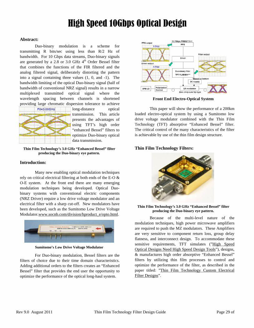
Abstract:
Duo-binary modulation is a scheme for transmitting R bits/sec using less than R/2 Hz of bandwidth. For 10 Gbps data streams, Duo-binary signals are generated by a 2.8 or 3.0 GHz 4th Order Bessel filter that combines the functions of the FIR filtered and the analog filtered signal, deliberately distorting the pattern into a signal containing three values (1, 0, and -1). The bandwidth limiting of the optical Duo-binary signal (half of bandwidth of conventional NRZ signal) results in a narrow multiplexed transmitted optical signal where the wavelength spacing between channels is shortened providing large chromatic dispersion tolerance to achieve
long-distance optical transmission. This article presents the advantages of using TFT’s high order “enhanced Bessel” filters to optimize Duo-binary optical data transmission.
Introduction:
Many new enabling optical modulation techniques rely on critical electrical filtering at both ends of the E-O & O-E system. At the front end there are many emerging modulation techniques being developed. Optical Duo-binary systems with conventional electric components (NRZ Driver) require a low drive voltage modulator and an electrical filter with a sharp cut-off. New modulators have been developed, such as the Sumitomo Low Drive Voltage Modulator.www.socnb.com/division/hproduct_e/opto.html.
For Duo-binary modulation, Bessel filters are the filters of choice due to their time domain characteristics. Adding additional orders to the filters creates an “Enhanced Bessel” filter that provides the end user the opportunity to optimize the performance of the optical long-haul system.
This paper will show the performance of a 200km loaded electro-optical system by using a Sumitomo low drive voltage modulator combined with the Thin Film Technology (TFT) absorptive “Enhanced Bessel” filter. The critical control of the many characteristics of the filter is achievable by use of the thin film design structure.
Thin Film Technology Filters:
Because of the multi-level nature of the modulation techniques, high power microwave amplifiers are required to push the MZ modulators. These Amplifiers are very sensitive to component return loss, group delay flatness, and interconnect design. To accommodate these sensitive requirements, TFT simulates (”High Speed Optical Designs Need High Speed Design Tools”), designs, & manufactures high order absorptive “Enhanced Bessel” filters by utilizing thin film processes to control and optimize the performance of the filter, as described in the paper titled: ”Thin Film Technology Custom Electrical Filter Designs”.
High Speed 10Gbps Optical Design
Thin Film Technology’s 3.0 GHz “Enhanced Bessel” filter producing the Duo-binary eye pattern.
Sumitomo’s Low Drive Voltage Modulator
Thin Film Technology’s 3.0 GHz “Enhanced Bessel” filter producing the Duo-binary eye pattern.
Front End Electro-Optical System

Rev 9.0 August 2011 Thin Film Technology Filter Design Guide Page 30 of
Test Setup:
The following 10 Gbps, 200km optical design demonstration was assembled. This demo used the TFT high order absorptive Enhanced Bessel filters.
Measured Results:
From the above 10 Gbps optical demonstration setup that included the Sumitomo low drive voltage modulator, three TFT 9th order “Enhanced Bessel” filters were tested, 2.75, 3.0, and 3.25 GHz. Testing on the above setup showed the FL9B 3.0Ghz filter to have the optimum results. The following plots show the performance results that were achieved:
Eye Patterns:
BER Waterfall Curves:
Conclusion:
This high speed 10 Gbps optical demonstration shows the benefits of combining TFT’s “Enhanced Bessel” filters, which exhibit exceptional time domain characteristics and low return loss, with the Sumitomo low drive voltage modulator for Duo-binary data transmission to provide better BER curves on the system output side. By utilizing thin films to realize high performance electrical filter components, TFT can simulate, design, and manufacture the custom filter component for your optical system by providing high performance service for your design support including fast turn custom prototypes to full production capacity start to finish.
High Speed 10Gbps Optical Design
Back-to-Back and After 3200ps/nm
Bit Error Rate
Power Penalty B-to-B 3200ps/nm
10-9 -17.2 dBm -16.1 dBm 1.1 dB
10-12 -16.4 dBm -14.9 dBm 1.5 dB
Received Power
Back-to-Back = Magenta and After 3200ps/nm = Blue
Power Penalty Comparison to a “Industry Std.” Filter

Rev 9.0 August 2011 Thin Film Technology Filter Design Guide Page 31 of
Overview:
Thin Film Technology (TFT) is a high-speed passive component manufacturer who can provide you with enhanced Bessel filters for your optical system designs. TFT utilizes thin film processes for high performance electrical filters that are used in the transmitter and receiver of high-speed electro-optical systems. Thin Film Technology Corporation can provide you with standard or custom “Enhanced Electrical Bessel” Filter components for both the front end and back end electrical subsystems in an optical system design. These filters provide an enhanced return loss and tight group delay design characteristics to help eliminate problems associated with reflected signals. Thin Film Technology can simulate, design, and manufacture a custom electrical filter component suitable for your optical system. Fast optical designs are realized using high performance service for your design support including fast turn custom prototypes to full production capacity start to finish. In addition to the custom filter design work, we also carry a standard set of 10 and 40 Gbps enhanced duo-binary electrical filters for your immediate needs.
Enhanced Bessel Filter for 40Gb/s:
TFT has been providing Bessel filters to the optical industry for maximum flat group delay performance and enhanced return loss. TFT’s enhanced Bessel Filters are 9th order low pass filters that matches the S21 parameter and group delay characteristics of an ideal 5th order Bessel filter, but provide improved return loss characteristics. Insertion loss specification of the filter is +/- 5% of the cutoff frequency. Forward
and reverse return loss specification is –13 dB up to the cutoff frequency in a surface mountable BGA package and is –12 dB up to 30 GHz in a wire-bondable package. Typical Group Delay is 10ps up to 1.5 times cutoff frequency. For 40 Gbps Duobinary systems, TFT manufactures a wide range of 9th order Enhanced Bessel filters having -3dB cut-off frequencies from 12GHz to 18GHz. We provide filters in Ball Grid Array (BGA) packages as well as in wire-bondable packages.
Simulation Services: Using Agilent's Advanced Design System RF Electronic Design Software, commonly known as ADS, Thin Film Technology will work with you to take your desired filter parameters (both electrical and mechanical) and input it into the simulation software.
The circuit design can be optimized to insure it will meet the specifications approved earlier. The circuit design is transferred to the ADS Momentum simulator. This layout simulator accounts for element interaction of the physical layout and can be used to further optimize the design. If needed, the ADS simulation software allows us to test and recommend circuit layout surrounding the filter to insure proper functioning when the physical device is realized.
Enhanced Bessel Filters for 40Gbps Systems
Typical S21 and S11; Phase and Group Delay
performance of TFT’s 40Gbps Enhanced Bessel Filter.

Rev 9.0 August 2011 Thin Film Technology Filter Design Guide Page 32 of
Wire-bondable Packaged Filter:
To maximize signal integrity performance, TFT offers filters in 1.95mm x 4.95mm package with gold plated pads for wire
bondable packages. The benefit of the wire-bondable package is the extension in the “footprint” bandwidth which minimizes the
influence to the enhanced Bessel filter’s performance. The below plot demonstrates the insertion loss performance of a TFT 15 GHz 9th order enhanced Bessel wire-bondable filter package in comparison to the ideal 5th order Bessel function. The probed part matches simulation through 20 GHz.BGA
BGA Packaged Filter: For lower cost and easy handling
capability TFT provide filters in 2.0 x 7.1mm BGA package. A thru trace in this 6-pin BGA package,
with the footprint, exhibits a component bandwidth of 30 GHz. The 30 GHz package bandwidth in series with the filter’s bandwidth (cut-off) will result in an overall filter package bandwidth lower than the ideal filter design, as shown in the plot below (for more information on this topic, please see the
TFT 40 Gbps filter package application note). The below S21 plot shows the simulated and measured (in TFT’s CMM) performance of BGA packaged 14.5 GHz 9th order enhanced Bessel filter.
Closing:
Thin Film Technology can provide you with standard or custom Enhanced Electrical Bessel Filter components for both the front end and back end electrical subsystems in a 10 and 40 Gbps optical system design. The “Enhanced Bessel” filters, which exhibit exceptional time domain characteristics and low return loss, are realized using high performance service for your design support including fast turn custom prototypes to full production capacity start to finish. TFT utilizes simulation techniques and also capitalizes on the advantages of thin film construction to realize these high performance electrical filter components. We can conceptualize, synthesize, and realize FAST!
Enhanced Bessel Filters for 40Gbps Systems

Rev 9.0 August 2011 Thin Film Technology Filter Design Guide Page 33 of
Introduction:
There are many microwave devices that are
not considered to be easily mounted in planar
circuit assemblies. Passive filters for optical
modulators are one of these. It was long
considered that you could not cut a surface mount
device into a multi-GHz path. These parts needed
to be coaxial modules or Gold wire bonded to
achieve the performance required by the 10 Gbps
plus applications.
As a very high-speed digital component
company, Thin Film Technology has developed
an open source coaxial measurement module
(CMM) that brings the reality of surface mount
10 and 40Gbps path components into the open.
By leaving the module open it is easy to see that
the filter function is provided by a single surface
mount component within a very realizable planar
environment.
TFT’s Coaxial Measurement Module:
These modules have 20GHz bandwidths and
beyond. When designing high-speed signal
integrity components, TFT considers the
footprint to be part of the component. The
component’s footprint is mated to a footprint on
the Rogers printed circuit board contained in the
CMM. The component, footprint, PCB coupon,
and module now provide the full working
environment for the component.
TFT’s CMMs typically demonstrate a family
of components such as low pass filters, high pass
equalizers, and attenuators for use in tuning a
systems performance on the designer’s test bench
before translating the component and footprint
directly into the end design.
Advantage to the End User:
The ability to tune the system on the bench
utilizing the component and its footprint is what
we call Reality Aided Design (RAD). The RAD
process allows us to see the impact of the
component tolerances and optimize the design for
best performance with the confidence from using
real devices and assembly processes. The ability
to directly transfer the component and associated
footprint out of the CMM onto a production
board allows the designer to fully characterize the
component in the real world environment prior to
final production assembly.
TFT Coaxial Modules in Reality Aided Design

Rev 9.0 August 2011 Thin Film Technology Filter Design Guide Page 34 of
General Thin Film Technology brings its engineering service to the customer in many facets including f i l t e r componen t r ecommenda t ions , demonstrating how to use filters in their specific applications, as well as full design simulation and prototype development. Simplifying the specification, development and testing of these types of devices is what we bring to our customers. Engineering from concept through realization is made practical and economical by the use of simulated measurement models, yield analysis, and real bench testing. Test Bench Tools and Services Thin Film Technology has a full line of coaxial bench tools to aid in your design, simulation, test, measurement, and calibration. Besides the complete line of high performance passive electronic SMT components, we have these components realized into coaxial measurement modules (CMM) to facilitate their capabilities on the bench. This allows for component level tuning to find the optimum
solution. We will also help in refining the existing capabilities to put you in front of your competition with s p e c i f i c c u s t o m c o m p o n e n t a n d i m p l e m e n t a t i o n technology.
Product Lines Enhanced Bessel Filters Equalizer (high pass filters) Performance chip resistors and networks Miniature High Speed Inductors Delay lines Low pass Filters Band pass Filters High speed Attenuators Power Splitters Antennas Integrated Passive Devices (IPD’s)
Thin Film Technology Engineering Services
Coaxial Measurement Modules (20GHz) Individual components (2 week Lead time) Part family Kit 2/Ea (4 week lead time) Calibration Grade Kit - 3/Ea + Traceable
engineering DATA (6week lead time) Your design - Custom Module footprint (4 weeks extra)
Consult factory for current pricing
Engineering and Design Services Design Simulation Modeling Prototyping Network Analysis Jitter analysis Failure analysis Environmental testing Custom microwave fixturing Microwave probing Shared Risk Approach Free upfront technical proposals complete non-disclosure protection Engineering Rate $/hr (consult factory) Technician Rate $/hr (consult factory) Simulation Rate $/hr (consult factory) Test Bench Rate $/hr (consult factory) Prototype lot run $ (consult factory) Design iterations $ (consult factory)
with lot run

Rev 9.0 August 2011 Thin Film Technology Filter Design Guide Page 35 of
_____________________________________________________________________
_____________________________________________________________________
_____________________________________________________________________
_____________________________________________________________________
_____________________________________________________________________
_____________________________________________________________________
_____________________________________________________________________
_____________________________________________________________________
_____________________________________________________________________
_____________________________________________________________________
_____________________________________________________________________
_____________________________________________________________________
_____________________________________________________________________
_____________________________________________________________________
_____________________________________________________________________
_____________________________________________________________________
_____________________________________________________________________
_____________________________________________________________________
_____________________________________________________________________
_____________________________________________________________________
_____________________________________________________________________
_____________________________________________________________________
_____________________________________________________________________
_____________________________________________________________________
_____________________________________________________________________
_____________________________________________________________________
_____________________________________________________________________
_____________________________________________________________________
_____________________________________________________________________
_____________________________________________________________________
_____________________________________________________________________
Your Notes

Rev 9.0 August 2011 Thin Film Technology Filter Design Guide Page 36 of
Thin Film Technology Corp. 1980 Commerce Drive
North Mankato, MN 56001 (USA)
Ph: (507) 625-8445 Fax: (507) 625-3523
Web: http://www.thin-film.com
How to Contact Thin Film Technology